MIC3490
High Input Voltage, Low IQ µCap LDO Regulator
Features
General Description
•
•
•
•
•
The MIC3490 is a 100 mA, highly accurate,
low-dropout regulator with high input voltage and
ultra-low ground current. This combination of high
voltage and low ground current makes the MIC3490
ideal for multi-cell Li-Ion battery systems.
•
•
•
•
•
•
•
Wide Input Voltage Range: 2.3V to 36V
Ultra-Low Ground Current: 18 µA
Low Dropout Voltage of 270 mV at 100 mA
High Output Accuracy of ±2.0% Overtemperature
µCap: Stable with Ceramic or Tantalum
Capacitors
Excellent Line and Load Regulation Specifications
Near Zero Shutdown Current: Typical 0.1 µA
Reverse Battery Protection
Reverse Leakage Protection
Thermal Shutdown and Current-Limit Protection
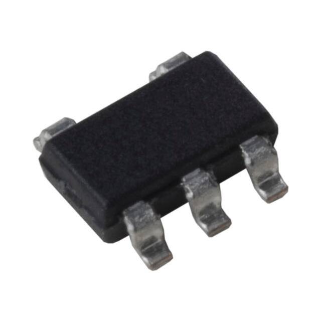
SOT23-5 Package
The MIC3490 is Pin-to-Pin Compatible with
LM3940
Applications
• Keep-Alive Supply in Notebook and Portable
Computers
• USB Power Supply
• Logic Supply for High-Voltage Batteries
• Automotive Electronics
• Battery-Powered Systems
• 3 to 4-Cell Li-Ion Battery Input Range
As a µCap LDO design, the MIC3490 is stable with
either ceramic or tantalum output capacitors. It only
requires a 2.2 µF output capacitor for stability.
Features of the MIC3490 include enable input, thermal
shutdown, current limit, reverse battery protection and
reverse leakage protection.
Available in five output voltage options (1.8V, 2.5V,
3.0V, 3.3V and 5.0V), the MIC3490 is offered in a 5-pin
SOT23 package with a junction temperature range of
-40°C to + 125°C.
Typical Application Circuit
Ultra-Low Current Adjustable Regulator
Application
MIC3490YM5
VIN
1
5
VOUT
2
OFF ON
CIN = 1.0 µF
2019 Microchip Technology Inc.
NC
3
EN
4
COUT = 2.2 µF
CERAMIC
IGND = 18 µA
DS20006137A-page 1
�MIC3490
Package Types
MIC3490
5-Pin SOT23
(Top View)
EN
3
GND
2
NC
1
L3XX
4
5
IN
OUT
Functional Block Diagrams
OUT
IN
EN
ENABLE
R1
VREF
R2
GND
DS20006137A-page 2
2019 Microchip Technology Inc.
�MIC3490
1.0
ELECTRICAL CHARACTERISTICS
Absolute Maximum Ratings †
Input Supply Voltage (VIN) ........................................................................................................................... -20V to +38V
Enable Input Voltage (VEN) ......................................................................................................................... -0.3V to +38V
Power Dissipation (PDIS)........................................................................................................................ Internally Limited
ESD Rating (Note 1) .................................................................................................................................. ESD Sensitive
Operating Ratings ‡
Input Supply Voltage (VIN) ......................................................................................................................... +2.3V to +36V
Enable Input Voltage (VEN) ............................................................................................................................. 0V to +36V
† Notice: Stresses above those listed under “Absolute Maximum Ratings” may cause permanent damage to the device.
This is a stress rating only and functional operation of the device at those or any other conditions above those indicated
in the operational sections of this specification is not intended. Exposure to maximum rating conditions for extended
periods may affect device reliability. Specifications are for packaged product only.
‡ Notice: The device is not ensured to function outside its operating ratings.
Note 1: Devices are ESD sensitive. Handling precautions are recommended.
TABLE 1-1:
ELECTRICAL CHARACTERISTICS
Electrical Characteristics: TJ = +25°C with VIN = VOUT + 1V; IOUT = 100 µA;
Bold values indicate -40°C ≤ TJ ≤ +125°C; unless otherwise specified. Specifications for packaged product only.
Parameter
Output Voltage Accuracy
Symbol
VOUT
Min.
Typ.
Max.
-1.0
—
1.0
-2.0
—
2.0
Units
Conditions
%
Variation from nominal VOUT
Line Regulation
ΔVOUT/ΔVIN
—
0.04
0.5
%
VIN = VOUT + 1V to 36V
Load Regulation
ΔVOUT/VOUT
—
0.25
1
%
IOUT = 100 µA to 100 mA
Dropout Voltage
Ground Current
Ground Current in Shutdown
Short-Circuit Current
Output Leakage, Reverse
Polarity Input (Note 2)
VDO
—
50
—
IOUT = 100 µA
—
230
300
IOUT = 50 mA
—
—
400
—
270
400
—
—
450
—
18
30
—
—
35
—
0.25
0.70
—
1
2
ISHDN
—
0.1
1
µA
ISC
—
190
350
mA
VOUT
—
-0.1
—
V
IGND
mV
IOUT = 100 mA
µA
mA
IOUT = 100 µA
IOUT = 50 mA
IOUT = 100 mA
VEN ≤ 0.6V; VIN = 36V
VOUT = 0V
Load = 500Ω; VIN = -15V
Enable Input
Input Low Voltage
Input High Voltage
Enable Input Current
Start-up Time
2019 Microchip Technology Inc.
VEN
—
—
0.6
2.0
—
—
-1.0
0.01
1.0
IEN
—
0.1
1.0
—
0.5
2.5
tSTART
—
1.7
7
V
Regulator off
Regulator on
VEN = 0.6V; Regulator off
µA
VEN = 2.0V; Regulator on
VEN = 36V; Regulator on
ms
VIN applied before EN signal
DS20006137A-page 3
�MIC3490
TEMPERATURE SPECIFICATIONS(1)
Parameters
Sym.
Min.
Typ.
Max.
Units
Conditions
Junction Operating Temperature Range
TJ
-40
—
+125
°C
—
Storage Temperature Range
TS
-65
—
+150
°C
—
JA
—
235
—
°C/W
—
Temperature Ranges
Package Thermal Resistances
Thermal Resistance 5-Pin SOT23
Note 1:
2:
The maximum allowable power dissipation is a function of ambient temperature, the maximum allowable
junction temperature and the thermal resistance from junction to air (i.e., TA, TJ, JA). Exceeding the
maximum allowable power dissipation will cause the device operating junction temperature to exceed the
maximum +125°C rating. Sustained junction temperatures above +125°C can impact the device reliability.
Design guidance only, not production tested.
DS20006137A-page 4
2019 Microchip Technology Inc.
�MIC3490
2.0
Note:
TYPICAL PERFORMANCE CURVES
The graphs and tables provided following this note are a statistical summary based on a limited number of
samples and are provided for informational purposes only. The performance characteristics listed herein
are not tested or guaranteed. In some graphs or tables, the data presented may be outside the specified
operating range (e.g., outside specified power supply range) and therefore outside the warranted range.
FIGURE 2-1:
Ratio.
Power Supply Rejection
FIGURE 2-4:
Dropout Characteristics.
FIGURE 2-2:
Current.
Dropout Voltage vs. Output
FIGURE 2-5:
Output Current.
Ground Pin Current vs.
FIGURE 2-3:
Temperature.
Dropout Voltage vs.
FIGURE 2-6:
Output Current.
Ground Pin Current vs.
2019 Microchip Technology Inc.
DS20006137A-page 5
�MIC3490
FIGURE 2-7:
Temperature.
Ground Pin Current vs.
FIGURE 2-10:
Input Voltage.
Ground Pin Current vs.
FIGURE 2-8:
Temperature.
Ground Pin Current vs.
FIGURE 2-11:
Input Voltage.
Ground Pin Current vs.
FIGURE 2-9:
Temperature.
Ground Pin Current vs.
FIGURE 2-12:
Input Voltage.
Ground Pin Current vs.
DS20006137A-page 6
2019 Microchip Technology Inc.
�MIC3490
FIGURE 2-13:
Voltage.
Input Current vs. Supply
FIGURE 2-14:
Temperature.
Output Voltage vs.
FIGURE 2-15:
Temperature.
Short-Circuit Current vs.
2019 Microchip Technology Inc.
FIGURE 2-16:
Load Transient Response.
DS20006137A-page 7
�MIC3490
3.0
PIN DESCRIPTIONS
The descriptions of the pins are listed in Table 3-1.
TABLE 3-1:
PIN FUNCTION TABLE
Pin Number
SOT23 (M5)
Pin
Name
1
NC
2
GND
3
EN
Enable (Input). Logic Low = Shutdown; Logic High = Enable.
4
IN
Supply Input.
5
OUT
DS20006137A-page 8
Description
No Connect.
Ground.
Regulator Output.
2019 Microchip Technology Inc.
�MIC3490
4.0
APPLICATION INFORMATION
4.1
Enable/Shutdown
The MIC3490 comes with an active-high enable pin
that allows the regulator to be disabled. Forcing the
enable pin low disables the regulator and sends it into
a “Zero” Off mode current state, consuming a typical
0.1 µA. Forcing the enable pin high enables the output
voltage.
4.2
Input Capacitor
The MIC3490 has a high input voltage capability, up
to 36V. The input capacitor must be rated to sustain
voltages that may be used on the input. An input capacitor may be required when the device is not near the
source power supply or when supplied by a battery.
Small surface mount, ceramic capacitors can be used
for bypassing. A larger value may be required if the
source supply has high ripple.
4.3
X7R/X5R dielectric-type ceramic capacitors are recommended because of their temperature performance.
X7R-type capacitors change capacitance by 15% over
their operating temperature range and are the most
stable type of ceramic capacitors. Z5U and Y5V dielectric capacitors change value by as much as 50% and
60%, respectively, over their operating temperature
ranges. To use a ceramic chip capacitor with Y5V
dielectric, the value must be much higher than an X7R
ceramic capacitor to ensure the same minimum
capacitance over the equivalent operating temperature
range.
No-Load Stability
The MIC3490 will remain stable and in regulation with
no load, unlike many other voltage regulators. This is
especially important in CMOS RAM keep-alive
applications.
4.5
EQUATION 4-1:
T J MAX – T A
PD MAX = --------------------------------
JA
Where:
TJ(MAX) =
Maximum junction temperature of
the die at +125°C
TA =
The ambient operating temperature
θJA =
Layout dependent
Table 4-1 shows examples of the junction-to-ambient
thermal resistance for the MIC3490:
TABLE 4-1:
Output Capacitor
The MIC3490 requires an output capacitor for stability.
The design requires 2.2 µF or greater on the output to
maintain stability. The design is optimized for use with
low-ESR ceramic chip capacitors. High-ESR capacitors
may cause high-frequency oscillation. The maximum
recommended ESR is 3Ω. The output capacitor can be
increased without limit. Larger valued capacitors help to
improve transient response.
4.4
To determine the maximum power dissipation of the
package, use the junction-to-ambient thermal resistance
of the device and Equation 4-1:
Thermal Consideration
5-PIN SOT23 THERMAL
RESISTANCE
Package
θJA Recommended
Minimum Footprint
SOT23-5
+235°C/W
The actual power dissipation of the regulator circuit can
be determined using Equation 4-2:
EQUATION 4-2:
P D = V IN – VOUT I OUT + VIN IGND
Substituting PD(MAX) for PD and solving for the operating
conditions that are critical to the application will give the
maximum operating conditions for the regulator circuit.
For example, when operating the MIC3490-3.0YM5 at
+50°C with a minimum footprint layout, the maximum
input voltage for a set output current can be determined
as follows:
EQUATION 4-3:
125 C – 50 C
P D MAX = -----------------------------------
235 C/W
Where:
PD(MAX) =
319 mW
The MIC3490 is designed to provide 100 mA of
continuous current in a very small package. Maximum
power dissipation can be calculated based on the
output current and the voltage drop across the part.
2019 Microchip Technology Inc.
DS20006137A-page 9
�MIC3490
The junction-to-ambient (θJA) thermal resistance for
the minimum footprint is +235°C/W from Table 4-1. It is
important that the maximum power dissipation not be
exceeded to ensure proper operation. Because the
MIC3490 was designed to operate with high input
voltages, careful consideration must be given so as not
to overheat the device. With very high input-to-output
voltage differentials, the output current is limited by the
total power dissipation.
Total power dissipation is calculated using the following
equation:
EQUATION 4-4:
P D = V IN – VOUT I OUT + VIN IGND
Due to the potential for input voltages up to 36V, ground
current must be taken into consideration.
If we know the maximum load current, we can solve for
the maximum input voltage using the maximum power
dissipation calculated for a +50°C ambient, 319 mW.
EQUATION 4-5:
P D MAX = V IN – VOUT I OUT + VIN IGND
Ground pin current is estimated using the typical
characteristics of the device.
EQUATION 4-6:
619 mW = VIN(102.8 mA)
Where:
VIN = 6.02V
For higher current outputs, only a lower input voltage
will work for higher ambient temperatures.
Assuming a lower output current of 10 mA, the
maximum input voltage can be recalculated:
EQUATION 4-7:
319mW = V IN – 3V 10mA + V IN 0.1mA
349mW = V IN 10.1mA
Where:
VIN = 34.55V
The maximum input voltage for a 10 mA load current at
+50°C ambient temperature is 34.55V, utilizing virtually
the entire operating voltage range of the device.
319mW = VIN – 3V 100mA + V IN 2.8mA
DS20006137A-page 10
2019 Microchip Technology Inc.
�MIC3490
5.0
PACKAGING INFORMATION
5.1
Package Marking Information
5-Lead SOT23* (2.9x1.6 mm)
Example
XXXX
TABLE 5-1:
L350
MIC3490 PACKAGE MARKING CODES
Part Number
Output Voltage
Marking Code
MIC3490-1.8YM5
1.8V
L318
MIC3490-2.5YM5
2.5V
L325
MIC3490-3.0YM5
3.0V
L330
MIC3490-3.3YM5
3.3V
L333
MIC3490-5.0YM5
5.0V
L350
Legend: XX...X
Y
YY
WW
NNN
e3
*
Product code or customer-specific information
Year code (last digit of calendar year)
Year code (last 2 digits of calendar year)
Week code (week of January 1 is week ‘01’)
Alphanumeric traceability code
Pb-free JEDEC® designator for Matte Tin (Sn)
This package is Pb-free. The Pb-free JEDEC designator ( e3 )
can be found on the outer packaging for this package.
●, ▲, ▼ Pin one index is identified by a dot, delta up, or delta down (triangle mark).
Note:
In the event the full Microchip part number cannot be marked on one line, it will
be carried over to the next line, thus limiting the number of available characters
for customer-specific information. Package may or may not include the corporate
logo.
Underbar (_) and/or Overbar (⎯) symbol may not be to scale.
2019 Microchip Technology Inc.
DS20006137A-page 11
�MIC3490
5.2
Package Details
The following sections give the technical details of the packages.
5-Lead Plastic Small Outline Transistor (OT) [SOT23]
Note:
For the most current package drawings, please see the Microchip Packaging Specification located at
http://www.microchip.com/packaging
0.20 C 2X
D
e1
A
D
N
E/2
E1/2
E1
E
(DATUM D)
(DATUM A-B)
0.15 C D
2X
NOTE 1
1
2
e
B
NX b
0.20
C A-B D
TOP VIEW
A
A A2
0.20 C
A
SEE SHEET 2
SEATING PLANE
A1
C
SIDE VIEW
Microchip Technology Drawing C04-091-OT Rev E Sheet 1 of 2
DS20006137A-page 12
2019 Microchip Technology Inc.
�MIC3490
5-Lead Plastic Small Outline Transistor (OT) [SOT23]
Note:
For the most current package drawings, please see the Microchip Packaging Specification located at
http://www.microchip.com/packaging
c
T
L
L1
VIEW A-A
SHEET 1
Units
Dimension Limits
Number of Pins
N
e
Pitch
e1
Outside lead pitch
Overall Height
A
Molded Package Thickness
A2
Standoff
A1
E
Overall Width
E1
Molded Package Width
D
Overall Length
L
Foot Length
Footprint
L1
I
Foot Angle
c
Lead Thickness
b
Lead Width
MIN
0.90
0.89
-
0.30
0°
0.08
0.20
MILLIMETERS
NOM
5
0.95 BSC
1.90 BSC
2.80 BSC
1.60 BSC
2.90 BSC
0.60 REF
-
MAX
1.45
1.30
0.15
0.60
10°
0.26
0.51
Notes:
1. Dimensions D and E1 do not include mold flash or protrusions. Mold flash or
protrusions shall not exceed 0.25mm per side.
2. Dimensioning and tolerancing per ASME Y14.5M
BSC: Basic Dimension. Theoretically exact value shown without tolerances.
REF: Reference Dimension, usually without tolerance, for information purposes only.
Microchip Technology Drawing C04-091-OT Rev E Sheet 2 of 2
2019 Microchip Technology Inc.
DS20006137A-page 13
�MIC3490
5-Lead Plastic Small Outline Transistor (OT) [SOT23]
Note:
For the most current package drawings, please see the Microchip Packaging Specification located at
http://www.microchip.com/packaging
X
SILK SCREEN
5
Y
Z
C
G
1
2
E
GX
RECOMMENDED LAND PATTERN
Units
Dimension Limits
E
Contact Pitch
C
Contact Pad Spacing
X
Contact Pad Width (X5)
Contact Pad Length (X5)
Y
Distance Between Pads
G
Distance Between Pads
GX
Overall Width
Z
MIN
MILLIMETERS
NOM
0.95 BSC
2.80
MAX
0.60
1.10
1.70
0.35
3.90
Notes:
1. Dimensioning and tolerancing per ASME Y14.5M
BSC: Basic Dimension. Theoretically exact value shown without tolerances.
Microchip Technology Drawing No. C04-2091B [OT]
DS20006137A-page 14
2019 Microchip Technology Inc.
�MIC3490
APPENDIX A:
REVISION HISTORY
Revision A (February 2019)
• Original Release of this Document
2019 Microchip Technology Inc.
DS20006137A-page 15
�MIC3490
NOTES:
DS20006137A-page 16
2019 Microchip Technology Inc.
�MIC3490
PRODUCT IDENTIFICATION SYSTEM
To order or obtain information, e.g., on pricing or delivery, contact your local Microchip representative or sales office.
PART NO.
-X.X
X
XXX
-XX
Device
Output
Voltage
Junction
Temperature
Range
Package
Media Type
Device:
MIC3490:
High Input Voltage, Low IQ µCap
LDO Regulator
1.8 = 1.8V
2.5 = 2.5V
Output Voltage:
3.0 = 3.0V
3.3 = 3.3V
5.0 = 5.0V
Junction
Temperature Range:
Y
Package:
M5 =
Media Type:
TR = 3000/Reel (SOT23 Only)
Examples:
a) MIC3490-1.8YM5-TR: High Input Voltage, Low IQ µCap
LDO Regulator, 1.8V, -40°C to
+125°C, SOT23-5, 3000/Reel
b) MIC3490-2.5YM5-TR: High Input Voltage, Low IQ µCap
LDO Regulator, 2.5V, -40°C to
+125°C, SOT23-5, 3000/Reel
c) MIC3490-3.0YM5-TR: High Input Voltage, Low IQ µCap
LDO Regulator, 3.0V, -40°C to
+125°C, SOT23-5, 3000/Reel
d) MIC3490-3.3YM5-TR: High Input Voltage, Low IQ µCap
LDO Regulator, 3.3V, -40°C to
+125°C, SOT23-5, 3000/Reel
e) MIC3490-5.0YM5-TR: High Input Voltage, Low IQ µCap
LDO Regulator, 5.0V, -40°C to
+125°C, SOT23-5, 3000/Reel
= -40°C to +125°C
Note 1:
5-Lead SOT23
2019 Microchip Technology Inc.
Tape and Reel identifier only appears in the
catalog part number description. This identifier is
used for ordering purposes and is not printed on
the device package. Check with your Microchip
Sales Office for package availability with the Tape
and Reel option.
DS20006137A-page 17
�MIC3490
NOTES:
DS20006137A-page 18
2019 Microchip Technology Inc.
�Note the following details of the code protection feature on Microchip devices:
•
Microchip products meet the specification contained in their particular Microchip Data Sheet.
•
Microchip believes that its family of products is one of the most secure families of its kind on the market today, when used in the
intended manner and under normal conditions.
•
There are dishonest and possibly illegal methods used to breach the code protection feature. All of these methods, to our
knowledge, require using the Microchip products in a manner outside the operating specifications contained in Microchip’s Data
Sheets. Most likely, the person doing so is engaged in theft of intellectual property.
•
Microchip is willing to work with the customer who is concerned about the integrity of their code.
•
Neither Microchip nor any other semiconductor manufacturer can guarantee the security of their code. Code protection does not
mean that we are guaranteeing the product as “unbreakable.”
Code protection is constantly evolving. We at Microchip are committed to continuously improving the code protection features of our
products. Attempts to break Microchip’s code protection feature may be a violation of the Digital Millennium Copyright Act. If such acts
allow unauthorized access to your software or other copyrighted work, you may have a right to sue for relief under that Act.
Information contained in this publication regarding device
applications and the like is provided only for your convenience
and may be superseded by updates. It is your responsibility to
ensure that your application meets with your specifications.
MICROCHIP MAKES NO REPRESENTATIONS OR
WARRANTIES OF ANY KIND WHETHER EXPRESS OR
IMPLIED, WRITTEN OR ORAL, STATUTORY OR
OTHERWISE, RELATED TO THE INFORMATION,
INCLUDING BUT NOT LIMITED TO ITS CONDITION,
QUALITY, PERFORMANCE, MERCHANTABILITY OR
FITNESS FOR PURPOSE. Microchip disclaims all liability
arising from this information and its use. Use of Microchip
devices in life support and/or safety applications is entirely at
the buyer’s risk, and the buyer agrees to defend, indemnify and
hold harmless Microchip from any and all damages, claims,
suits, or expenses resulting from such use. No licenses are
conveyed, implicitly or otherwise, under any Microchip
intellectual property rights unless otherwise stated.
Trademarks
Microchip received ISO/TS-16949:2009 certification for its worldwide
headquarters, design and wafer fabrication facilities in Chandler and
Tempe, Arizona; Gresham, Oregon and design centers in California
and India. The Company’s quality system processes and procedures
are for its PIC® MCUs and dsPIC® DSCs, KEELOQ® code hopping
devices, Serial EEPROMs, microperipherals, nonvolatile memory and
analog products. In addition, Microchip’s quality system for the design
and manufacture of development systems is ISO 9001:2000 certified.
SQTP is a service mark of Microchip Technology Incorporated in
the U.S.A.
QUALITY MANAGEMENT SYSTEM
CERTIFIED BY DNV
The Microchip name and logo, the Microchip logo, AnyRate, AVR,
AVR logo, AVR Freaks, BitCloud, chipKIT, chipKIT logo,
CryptoMemory, CryptoRF, dsPIC, FlashFlex, flexPWR, Heldo,
JukeBlox, KeeLoq, Kleer, LANCheck, LINK MD, maXStylus,
maXTouch, MediaLB, megaAVR, MOST, MOST logo, MPLAB,
OptoLyzer, PIC, picoPower, PICSTART, PIC32 logo, Prochip
Designer, QTouch, SAM-BA, SpyNIC, SST, SST Logo,
SuperFlash, tinyAVR, UNI/O, and XMEGA are registered
trademarks of Microchip Technology Incorporated in the U.S.A.
and other countries.
ClockWorks, The Embedded Control Solutions Company,
EtherSynch, Hyper Speed Control, HyperLight Load, IntelliMOS,
mTouch, Precision Edge, and Quiet-Wire are registered
trademarks of Microchip Technology Incorporated in the U.S.A.
Adjacent Key Suppression, AKS, Analog-for-the-Digital Age, Any
Capacitor, AnyIn, AnyOut, BodyCom, CodeGuard,
CryptoAuthentication, CryptoAutomotive, CryptoCompanion,
CryptoController, dsPICDEM, dsPICDEM.net, Dynamic Average
Matching, DAM, ECAN, EtherGREEN, In-Circuit Serial
Programming, ICSP, INICnet, Inter-Chip Connectivity,
JitterBlocker, KleerNet, KleerNet logo, memBrain, Mindi, MiWi,
motorBench, MPASM, MPF, MPLAB Certified logo, MPLIB,
MPLINK, MultiTRAK, NetDetach, Omniscient Code Generation,
PICDEM, PICDEM.net, PICkit, PICtail, PowerSmart, PureSilicon,
QMatrix, REAL ICE, Ripple Blocker, SAM-ICE, Serial Quad I/O,
SMART-I.S., SQI, SuperSwitcher, SuperSwitcher II, Total
Endurance, TSHARC, USBCheck, VariSense, ViewSpan,
WiperLock, Wireless DNA, and ZENA are trademarks of
Microchip Technology Incorporated in the U.S.A. and other
countries.
Silicon Storage Technology is a registered trademark of Microchip
Technology Inc. in other countries.
GestIC is a registered trademark of Microchip Technology
Germany II GmbH & Co. KG, a subsidiary of Microchip
Technology Inc., in other countries.
All other trademarks mentioned herein are property of their
respective companies.
© 2019, Microchip Technology Incorporated, All Rights Reserved.
ISBN: 978-1-5224-4154-0
== ISO/TS 16949 ==
2019 Microchip Technology Inc.
DS20006137A-page 19
�Worldwide Sales and Service
AMERICAS
ASIA/PACIFIC
ASIA/PACIFIC
EUROPE
Corporate Office
2355 West Chandler Blvd.
Chandler, AZ 85224-6199
Tel: 480-792-7200
Fax: 480-792-7277
Technical Support:
http://www.microchip.com/
support
Web Address:
www.microchip.com
Australia - Sydney
Tel: 61-2-9868-6733
India - Bangalore
Tel: 91-80-3090-4444
China - Beijing
Tel: 86-10-8569-7000
India - New Delhi
Tel: 91-11-4160-8631
Austria - Wels
Tel: 43-7242-2244-39
Fax: 43-7242-2244-393
China - Chengdu
Tel: 86-28-8665-5511
India - Pune
Tel: 91-20-4121-0141
Denmark - Copenhagen
Tel: 45-4450-2828
Fax: 45-4485-2829
China - Chongqing
Tel: 86-23-8980-9588
Japan - Osaka
Tel: 81-6-6152-7160
Finland - Espoo
Tel: 358-9-4520-820
China - Dongguan
Tel: 86-769-8702-9880
Japan - Tokyo
Tel: 81-3-6880- 3770
China - Guangzhou
Tel: 86-20-8755-8029
Korea - Daegu
Tel: 82-53-744-4301
France - Paris
Tel: 33-1-69-53-63-20
Fax: 33-1-69-30-90-79
China - Hangzhou
Tel: 86-571-8792-8115
Korea - Seoul
Tel: 82-2-554-7200
China - Hong Kong SAR
Tel: 852-2943-5100
Malaysia - Kuala Lumpur
Tel: 60-3-7651-7906
China - Nanjing
Tel: 86-25-8473-2460
Malaysia - Penang
Tel: 60-4-227-8870
China - Qingdao
Tel: 86-532-8502-7355
Philippines - Manila
Tel: 63-2-634-9065
China - Shanghai
Tel: 86-21-3326-8000
Singapore
Tel: 65-6334-8870
China - Shenyang
Tel: 86-24-2334-2829
Taiwan - Hsin Chu
Tel: 886-3-577-8366
China - Shenzhen
Tel: 86-755-8864-2200
Taiwan - Kaohsiung
Tel: 886-7-213-7830
China - Suzhou
Tel: 86-186-6233-1526
Taiwan - Taipei
Tel: 886-2-2508-8600
China - Wuhan
Tel: 86-27-5980-5300
Thailand - Bangkok
Tel: 66-2-694-1351
China - Xian
Tel: 86-29-8833-7252
Vietnam - Ho Chi Minh
Tel: 84-28-5448-2100
Atlanta
Duluth, GA
Tel: 678-957-9614
Fax: 678-957-1455
Austin, TX
Tel: 512-257-3370
Boston
Westborough, MA
Tel: 774-760-0087
Fax: 774-760-0088
Chicago
Itasca, IL
Tel: 630-285-0071
Fax: 630-285-0075
Dallas
Addison, TX
Tel: 972-818-7423
Fax: 972-818-2924
Detroit
Novi, MI
Tel: 248-848-4000
Houston, TX
Tel: 281-894-5983
Indianapolis
Noblesville, IN
Tel: 317-773-8323
Fax: 317-773-5453
Tel: 317-536-2380
Los Angeles
Mission Viejo, CA
Tel: 949-462-9523
Fax: 949-462-9608
Tel: 951-273-7800
Raleigh, NC
Tel: 919-844-7510
New York, NY
Tel: 631-435-6000
San Jose, CA
Tel: 408-735-9110
Tel: 408-436-4270
Canada - Toronto
Tel: 905-695-1980
Fax: 905-695-2078
DS20006137A-page 20
China - Xiamen
Tel: 86-592-2388138
China - Zhuhai
Tel: 86-756-3210040
Germany - Garching
Tel: 49-8931-9700
Germany - Haan
Tel: 49-2129-3766400
Germany - Heilbronn
Tel: 49-7131-67-3636
Germany - Karlsruhe
Tel: 49-721-625370
Germany - Munich
Tel: 49-89-627-144-0
Fax: 49-89-627-144-44
Germany - Rosenheim
Tel: 49-8031-354-560
Israel - Ra’anana
Tel: 972-9-744-7705
Italy - Milan
Tel: 39-0331-742611
Fax: 39-0331-466781
Italy - Padova
Tel: 39-049-7625286
Netherlands - Drunen
Tel: 31-416-690399
Fax: 31-416-690340
Norway - Trondheim
Tel: 47-7288-4388
Poland - Warsaw
Tel: 48-22-3325737
Romania - Bucharest
Tel: 40-21-407-87-50
Spain - Madrid
Tel: 34-91-708-08-90
Fax: 34-91-708-08-91
Sweden - Gothenberg
Tel: 46-31-704-60-40
Sweden - Stockholm
Tel: 46-8-5090-4654
UK - Wokingham
Tel: 44-118-921-5800
Fax: 44-118-921-5820
2019 Microchip Technology Inc.
08/15/18
�