MIC4451/52
12A Peak Low-Side MOSFET Drivers
Features
General Description
• BiCMOS/DMOS Construction
• Latch-Up Proof: Fully Isolated Process is
Inherently Immune to Any Latch-Up
• Input Will Withstand Negative Swing of up to 5V
• Matched Rise and Fall Times: 25 ns
• High Peak Output Current: 12A
• Wide Operating Range: 4.5V to 18V
• High Capacitive Load Drive: 62,000 pF
• Low Delay Time: 30 ns (typ.)
• Logic High Input for Any Voltage from 2.4V to VS
• Low Supply Current 450 µA with Logic 1 Input
• Low Output Impedance: 1.0Ω
• Output Voltage Swing to within 25 mV of GND or
VS
• Low Equivalent Input Capacitance: 7 pF (typ.)
The MIC4451 and MIC4452 CMOS MOSFET drivers
are robust, efficient, and easy to use. The MIC4451 is
an inverting driver, while the MIC4452 is a
non-inverting driver.
Applications
•
•
•
•
•
•
•
•
Switch Mode Power Supplies
Motor Controls
Pulse Transformer Driver
Class-D Switching Amplifier
Line Drivers
Driving MOSFET or IGBT Parallel Chip Modules
Local Power ON/OFF Switch
Pulse Generators
Both versions are capable of 12A (peak) output and
can drive the largest MOSFETs with an improved safe
operating margin. The MIC4451/52 accept any logic
input from 2.4V to VS without external speed-up
capacitors or resistor networks. Proprietary circuits
allow the input to swing negative by as much as 5V
without damaging the part. Additional circuits protect
against damage from electrostatic discharge.
MIC4451/52 drivers can replace three or more discrete
components, reducing PCB area requirements,
simplifying product design, and reducing assembly
cost.
Modern Bipolar/CMOS/DMOS construction ensures
freedom from latch-up. The rail-to-rail swing capability
of CMOS/DMOS ensures adequate gate voltage to the
MOSFET during power up/down sequencing. Because
these devices are fabricated on a self-aligned process,
they have very low crossover current, run cool, use little
power, and are easy to drive.
Package Types
MIC4451, MIC4452
8-Lead SOIC (M)
8-Lead PDIP (N)
(Top View)
VS 1
8 VS
IN 2
7 OUT
NC 3
6 OUT
GND 4
5 GND
2021 Microchip Technology Inc. and its subsidiaries
MIC4451, MIC4452
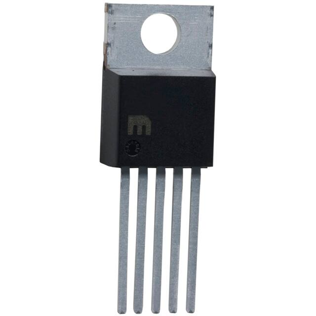
5-Lead TO-220 (T)
(Top View)
5
4
3
2
1
OUT
GND
VS
GND
IN
DS20006616A-page 1
�MIC4451/52
Functional Block Diagram
VS
0.3mA
MIC4451
INVERTING
0.1mA
OUT
IN
2k
MIC4452
NONINVERTING
GND
DS20006616A-page 2
2021 Microchip Technology Inc. and its subsidiaries
�MIC4451/52
1.0
ELECTRICAL CHARACTERISTICS
Absolute Maximum Ratings †
Supply Voltage ..........................................................................................................................................................+20V
Input Voltage ................................................................................................................................ VS + 0.3V to GND – 5V
Input Current (VIN > VS) ............................................................................................................................................5 mA
Power Dissipation (TA ≤ 25°C)
PDIP.................................................................................................................................................................960 mW
SOIC ..............................................................................................................................................................1040 mW
TO-220 .....................................................................................................................................................................2W
Power Dissipation (TCASE ≤ 25°C)
TO-220 ................................................................................................................................................................12.5W
Derating Factors (to Ambient)
PDIP.............................................................................................................................................................7.7 mW/°C
SOIC ............................................................................................................................................................8.3 mW/°C
TO-220 ..........................................................................................................................................................17 mW/°C
† Notice: Stresses above those listed under “Absolute Maximum Ratings” may cause permanent damage to the device.
This is a stress rating only and functional operation of the device at those or any other conditions above those indicated
in the operational sections of this specification is not intended. Exposure to maximum rating conditions for extended
periods may affect device reliability. Static-sensitive device. Store only in conductive containers. Handling personnel and
equipment should be grounded to prevent damage from static discharge.
ELECTRICAL CHARACTERISTICS
Electrical Characteristics: TA = +25°C, with 4.5V ≤ VS ≤ 18V unless otherwise specified.
Parameter
Symbol
Min.
Typ.
Max.
Units
Conditions
Logic 1 Input Voltage
VIH
2.4
1.3
—
V
—
Logic 0 Input Voltage
VIL
—
1.1
0.8
V
—
V
—
Input
Input Voltage Range
VIN
–5
—
VS +
0.3
Input Current
IIN
–10
—
10
µA
0V ≤ VIN ≤ VS
High Output Voltage
VOH
VS –
0.025
—
—
V
See Figure 1-1.
Output
Low Output Voltage
VOL
—
—
0.025
V
See Figure 1-1.
Output Resistance,
Output High
RO
—
0.6
1.5
Ω
IOUT = 10 mA, VS = 18V
Output Resistance,
Output Low
RO
—
0.8
1.5
Ω
IOUT = 10 mA, VS = 18V
Peak Output Current
IPK
—
12
—
A
VS = 18V, see Figure 1-3
Continuous Output
Current
IDC
2
—
—
A
—
Latch-up Protection
Withstand Reverse
Current
IR
>1500
—
—
mA
Duty Cycle ≤ 2%, t ≤ 300 μs
tR
—
20
40
ns
See Figure 1-1. CL = 15,000 pF
Fall Time
tF
—
24
50
ns
See Figure 1-1. CL = 15,000 pF
Delay Time
tD1
—
25
50
ns
See Figure 1-1.
Delay Time
tD2
—
40
60
ns
See Figure 1-1.
Switching Time (Note 1)
Rise Time
2021 Microchip Technology Inc. and its subsidiaries
DS20006616A-page 3
�MIC4451/52
ELECTRICAL CHARACTERISTICS (CONTINUED)
Electrical Characteristics: TA = +25°C, with 4.5V ≤ VS ≤ 18V unless otherwise specified.
Parameter
Symbol
Min.
Typ.
Max.
Units
—
—
4.5
Conditions
0.4
1.5
mA
VIN = 3V
80
150
µA
VIN = 0V
—
18
V
—
Power Supply
Power Supply Current
IS
Operating Input Voltage
VS
Note 1:
Specification for packaged product only.
ELECTRICAL CHARACTERISTICS
Electrical Characteristics: Over operating temperature range with 4.5V ≤ VS ≤ 18V unless otherwise specified.
Parameter
Symbol
Min.
Typ.
Max.
Units
Conditions
Input
Logic 1 Input Voltage
VIH
2.4
—
—
V
—
Logic 0 Input Voltage
VIL
—
—
0.8
V
—
Input Voltage Range
VIN
–5
—
VS +
0.3
V
—
Input Current
IIN
–10
—
10
µA
0V ≤ VIN ≤ VS
High Output Voltage
VOH
VS –
0.025
—
—
V
See Figure 1-1.
Low Output Voltage
VOL
—
—
0.025
V
See Figure 1-1.
Output Resistance,
Output High
RO
—
—
2.2
Ω
IOUT = 10 mA, VS = 18V
Output Resistance,
Output Low
RO
—
—
2.2
Ω
IOUT = 10 mA, VS = 18V
Rise Time
tR
—
—
50
ns
See Figure 1-1. CL = 15,000 pF
Fall Time
tF
—
—
60
ns
See Figure 1-1. CL = 15,000 pF
Delay Time
tD1
—
—
65
ns
See Figure 1-1.
Delay Time
tD2
—
—
80
ns
See Figure 1-1.
—
—
3
—
—
0.4
4.5
—
18
Output
Switching Time (Note 1)
Power Supply
Power Supply Current
IS
Operating Input Voltage
VS
Note 1:
mA
V
VIN = 3V
VIN = 0V
—
Specification for packaged product only.
DS20006616A-page 4
2021 Microchip Technology Inc. and its subsidiaries
�MIC4451/52
TEMPERATURE SPECIFICATIONS (Note 1)
Parameters
Sym.
Min.
Typ.
Max.
Units
Conditions
0
—
+70
°C
Z Ordering Option
–40
—
+85
°C
Y Ordering Option
–40
—
+125
°C
V Ordering Option
Temperature Ranges
Ambient Operating Temperature Range
TA
Storage Temperature Range
TS
–65
—
+150
°C
—
Chip Operating Temperature
—
—
—
+150
°C
—
Lead Temperature
—
—
—
+300
°C
Soldering, 10 sec.
θJC
—
10
—
°C/W
Package Thermal Resistance
Thermal Resistance, TO-220 5-Ld
Note 1:
—
The maximum allowable power dissipation is a function of ambient temperature, the maximum allowable
junction temperature and the thermal resistance from junction to air (i.e., TA, TJ, JA). Exceeding the
maximum allowable power dissipation will cause the device operating junction temperature to exceed the
maximum +125°C rating. Sustained junction temperatures above +125°C can impact the device reliability.
Test Circuits
FIGURE 1-1:
Time.
Inverting Driver Switching
FIGURE 1-3:
Peak Output Current Test Circuit.
2021 Microchip Technology Inc. and its subsidiaries
FIGURE 1-2:
Switching Time.
Non-Inverting Driver
DS20006616A-page 5
�MIC4451/52
2.0
Note:
TYPICAL PERFORMANCE CURVES
The graphs and tables provided following this note are a statistical summary based on a limited number of
samples and are provided for informational purposes only. The performance characteristics listed herein
are not tested or guaranteed. In some graphs or tables, the data presented may be outside the specified
operating range (e.g., outside specified power supply range) and therefore outside the warranted range.
FIGURE 2-1:
Voltage.
Rise Time vs. Supply
FIGURE 2-4:
Load.
Rise Time vs. Capacitive
FIGURE 2-2:
Voltage.
Fall Time vs. Supply
FIGURE 2-5:
Load.
Fall Time vs. Capacitive
FIGURE 2-3:
Temperature.
Rise and Fall Times vs.
FIGURE 2-6:
Supply Voltage.
Crossover Energy vs.
DS20006616A-page 6
2021 Microchip Technology Inc. and its subsidiaries
�MIC4451/52
FIGURE 2-7:
Capacitive Load.
Supply Current vs.
FIGURE 2-10:
Frequency.
Supply Current vs.
FIGURE 2-8:
Capacitive Load.
Supply Current vs.
FIGURE 2-11:
Frequency.
Supply Current vs.
FIGURE 2-9:
Capacitive Load.
Supply Current vs.
FIGURE 2-12:
Frequency.
Supply Current vs.
2021 Microchip Technology Inc. and its subsidiaries
DS20006616A-page 7
�MIC4451/52
FIGURE 2-13:
vs. Temperature.
FIGURE 2-16:
Amplitude.
Propagation Delay vs. Input
FIGURE 2-14:
High-State Output
Resistance vs. Supply Voltage.
FIGURE 2-17:
Amplitude.
Propagation Delay vs. Input
FIGURE 2-15:
Low-State Output
Resistance vs. Supply Voltage.
FIGURE 2-18:
Temperature.
Propagation Delay vs. Input
DS20006616A-page 8
Quiescent Supply Current
2021 Microchip Technology Inc. and its subsidiaries
�MIC4451/52
3.0
PIN DESCRIPTIONS
The descriptions of the pins are listed in Table 3-1.
TABLE 3-1:
Pin Number
TO-220
PIN FUNCTION TABLE
Pin Number
SOIC/PDIP
Pin Name
1
2
IN
2, 4
4, 5
GND
3, TAB
1, 8
VS
5
6, 7
OUT
—
3
NC
2021 Microchip Technology Inc. and its subsidiaries
Description
Control Input.
Ground: Duplicate Pins must be externally connected together.
Supply Input: Duplicate pins must be externally connected together.
Output: Duplicate pins must be externally connected together.
Not Connected.
DS20006616A-page 9
�MIC4451/52
4.0
APPLICATIONS INFORMATION
4.1
Supply Bypassing
Charging and discharging large capacitive loads
quickly requires large currents. For example, changing
a 10,000 pF load to 18V in 50 ns requires 3.6A.
The MIC4451 and MIC4452 have double bonding on
the supply pins, the ground pins, and output pins. This
reduces parasitic lead inductance. Low inductance
enables large currents to be switched rapidly. It also
reduces internal ringing that can cause voltage
breakdown when the driver is operated at or near the
maximum rated voltage.
Internal ringing can also cause output oscillation due to
feedback. This feedback is added to the input signal
because it is referenced to the same ground.
To ensure low supply impedance over a wide frequency
range, a parallel capacitor combination is
recommended for supply bypassing. Low inductance
ceramic disc capacitors with short lead lengths
(


 工商网监
湘ICP备2023018690号
工商网监
湘ICP备2023018690号