MIC4478/4479/4480
32V Low-Side Dual MOSFET Drivers
General Description
Features
The MIC4478, MIC4479, and MIC4480 are low-side dual
MOSFET drivers are designed to switch N-channel
enhancement type MOSFETs from TTL-compatible control
signals for low-side switch applications. The MIC4478 is
dual non-inverting, the MIC4479 is dual inverting, and the
MIC4480 is complimentary non-inverting and inverting.
These drivers feature short delays and high peak currents
to produce precise edges and rapid rise and fall times.
• +4.5V to +32V operation
• 300µA typical supply quiescent current
• 2.5A nominal peak output per channel
− 6Ω high-side typical output resistance
− 3Ω low-side typical output resistance
• Active-high driver enable inputs with internal pull-ups
• Operates with low-side switch circuits
• –40°C to +125°C ambient temperature range
• ESD protection
• Dual inverting, dual non-inverting, and inverting + noninverting versions
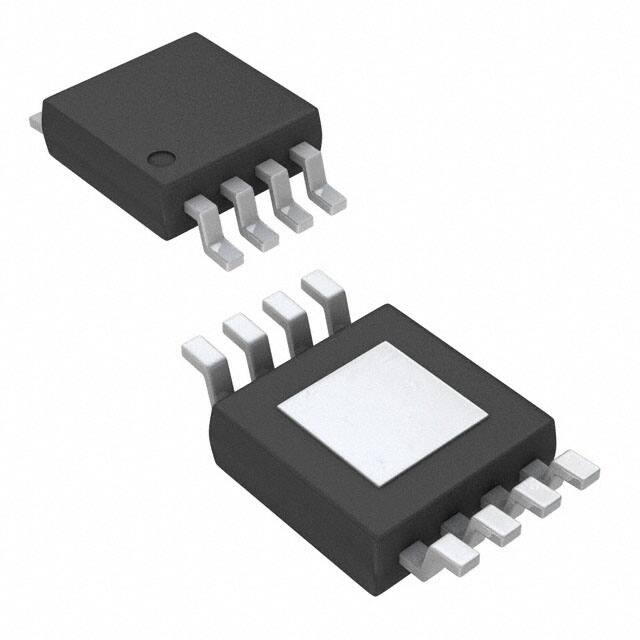
• 8-pin SOIC (ePAD and non-ePAD)
The MIC4478/4479/4480 are powered from a +4.5V to
+32V supply voltage. The on-state gate drive output
voltage is approximately equal to the supply voltage (no
internal regulators or clamps).
In a low-side configuration, the drivers can control a
MOSFET that switches any voltage up to the rating of the
MOSFET. The MIC4478/4479/4480 are available in the 8lead SOIC (ePAD and non-ePAD) package and are rated
for the –40°C to +125°C ambient temperature range.
Datasheets and support documentation are available on
Micrel’s web site at: www.micrel.com.
Applications
• Synchronous switch-mode power supplies
• Secondary side synchronous rectification
Typical Application
Micrel Inc. • 2180 Fortune Drive • San Jose, CA 95131 • USA • tel +1 (408) 944-0800 • fax + 1 (408) 474-1000 • http://www.micrel.com
December 9, 2014
Revision 1.0
�Micrel, Inc.
MIC4478/4479/4480
Ordering Information
Part Number
Marking
Configuration
Junction Temp. Range
Package
Lead Finish
MIC4478YM
4478YM
Dual Non-Inverting
–40°C to +125°C
8-pin SOIC
Pb-Free
4478YME
Dual Non-Inverting
–40°C to +125°C
8-pin ePAD SOIC
Pb-Free
4479YM
Dual Inverting
–40°C to +125°C
8-pin SOIC
Pb-Free
4479YME
Dual Inverting
–40°C to +125°C
8-pin ePAD SOIC
Pb-Free
4480YM
Inverting + Non-Inverting
–40°C to +125°C
8-pin SOIC
Pb-Free
4480YME
Inverting + Non-Inverting
–40°C to +125°C
8-pin ePAD SOIC
Pb-Free
MIC4478YME
MIC4479YM
MIC4479YME
MIC4480YM
MIC4480YME
Pin Configurations
December 9, 2014
2
Revision 1.0
�Micrel, Inc.
MIC4478/4479/4480
Pin Description
Pin Number
MIC4478
Pin Number
MIC4479
1
1
Pin Number
MIC4480
1
Pin Name
Pin Description
ENA
Enable pin channel A. TTL-compatible enabling/disabling of the
device. An internal pull-up enables the device if this pin is
floating or unconnected. A logic-low voltage disables the device
and the output (OUTA) will be pulled to ground regardless of the
input state.
2
2
2
INA
Input channel A. TTL-compatible on/off control input.
MIC4478 only: A logic-high forces the output (OUTA) to the
supply voltage. A logic-low forces OUTA to ground.
MIC4479 only: A logic-low forces the output (/OUTA) to the
supply voltage. A logic-high forces /OUTA to ground.
MIC4480 only: Complimentary logic-low/high (INA/INB) forces
the output (/OUTA) to the supply voltage. Complimentary logichigh/high (INA/INB) forces /OUTA to ground.
3
3
3
GND
Ground. Power return.
4
4
4
INB
Input channel B. TTL-compatible on/off control input.
MIC4478 only: A logic-high forces the output (OUTB) to the
supply voltage. A logic-low forces OUTB to ground.
MIC4479 only: A logic-low forces the output (/OUTB) to the
supply voltage. A logic-high forces /OUTB to ground.
MIC4480 only: Complimentary logic-low/high (INA/INB) forces
the output (OUTB) to the supply voltage. Complimentary logichigh/high (INA/INB) forces OUTB to ground.
5
-
5
OUTB
Channel B Output (Non-Inverting). Gate drive connection to the
external MOSFET.
-
5
-
/OUTB
Channel B Output (Inverting). Gate drive connection to the
external MOSFET.
6
6
6
VS
Supply Input. +4.5V to +32V supply.
7
-
-
OUTA
Channel A Output (Non-Inverting). Gate drive connection to the
external MOSFET.
-
7
7
/OUTA
Channel A Output (Inverting). Gate drive connection to the
external MOSFET.
8
8
8
ENB
Enable pin channel B. TTL-compatible enabling/disabling of the
device. An internal pull-up enables the device if this pin is
floating or unconnected. A logic-low voltage disables the device
and the output (OUTB) will be pulled to ground regardless of the
input state.
EP
EP
EP
ePAD
Ground. Exposed pad of the YME package option. Connect this
pad to GND for best thermal performance.
December 9, 2014
3
Revision 1.0
�Micrel, Inc.
MIC4478/4479/4480
Absolute Maximum Ratings(1)
Operating Ratings(2)
Supply Voltage (VS) ....................................... –0.3V to +36V
Input Voltage (VINA, VINB) ............................... –0.3V to +36V
Enable Voltage (VENA, VENB) .......................... –0.3V to +36V
Output Voltage (VOUTA, VOUTB) ....................... –0.3V to +36V
Junction Temperature (TJ) ......................................... 150°C
Lead Temperature (soldering, 10s) ............................ 260°C
Ambient Storage Temperature (TS)........... –65°C to +150°C
ESD Rating(3)
Machine Model ...................................................... 200V
Human Body Model ................................................. 2kV
Supply Voltage (VS)....................................... +4.5V to +32V
Input Voltage (VINA, VINB) ......................................... 0V to VS
Enable Voltage (VENA, VENB) .................................... 0V to VS
Ambient Temperature (TA) ........................ –40°C to +125°C
Junction Thermal Resistance
8 pin-SOIC (θJA) ................................................. 63°C/W
8 pin-ePAD SOIC (θJA) ...................................... 40°C/W
Electrical Characteristics(4)
VS =12V; TA = 25°C, bold values indicate -40°C ≤ TJ ≤ +125°C, unless noted.
Symbol
Parameter
Condition
Min.
Typ.
Max.
Units
32
V
300
600
µA
300
600
µA
300
600
µA
Supply
VS
4.5
Supply Voltage Range
VENA, VENB = open; VINA, VINB = 5V/5V (MIC4478)
VENA, VENB = open; VINA, VINB = 0V/0V (MIC4478)
VENA, VENB = 0V; VINA, VINB = 5V/5V (MIC4478)
VENA, VENB = 0V; VINA, VINB = 0V/0V (MIC4478)
VENA, VENB = open; VINA, VINB = 0V/0V (MIC4479)
IS
Quiescent Current
VENA, VENB = open; VINA, VINB = 5V/5V (MIC4479)
VENA, VENB = 0V; VINA, VINB = 0V/0V (MIC4479)
VENA, VENB = 0V; VINA, VINB = 5V/5V (MIC4479)
VENA, VENB = open; VINA, VINB = 0V/5V (MIC4480)
VENA, VENB = open; VINA,INB = 5V/0V (MIC4480)
VENA, VENB = 0V; VINA,INB = 0V/5V (MIC4480)
VENA, VENB=0V; VINA,INB = 5V/0V (MIC4480)
Input
VINA, VINB → logic 1 input
VINA,INB
Input Voltage
2.4
V
VINA, VINB → logic 0 input
0.8
Hysteresis voltage
IINA,INB
Input Current
0V ≤ VINA,INB ≤ VS
tRD,INA,INB
Rising delay time:
VINA,INB to VOUTA, VOUTB
tFD,INA,INB
Falling delay time:
VINA, VINB to VOUTA, VOUTB
0.3
–10
V
V
10
µA
VS = 12V; CL = 1000Pf
160
ns
VS = 30V; CL = 1000pF
160
ns
VS = 12V; CL = 1000pF
70
ns
VS = 30V; CL = 1000pF
70
ns
Notes:
1. Exceeding the absolute maximum ratings may damage the device.
2. The device is not guaranteed to function outside its operating ratings.
3. Devices are ESD sensitive. Handling precautions are recommended. Human body model, 1.5kΩ in series with 100pF.
4. Specification for packaged product only.
December 9, 2014
4
Revision 1.0
�Micrel, Inc.
MIC4478/4479/4480
Electrical Characteristics(4) (Continued)
VS = 12V; TJ = 25°C, bold values indicate -40°C ≤ TJ ≤ +125°C, unless noted.
Symbol
Parameter
Condition
Min.
Typ.
Max.
Units
Enable
2.4
VEN logic 1 input
VENA, VENB
Enable Voltage
0.8
VEN logic 0 input
Hysteresis voltage
Enable Current
0V ≤ VENA, VENB ≤ VS
tR
Rise Time:
Output VOUTA, VOUTB
tF
Fall Time:
Output VOUTA, VOUTB
ZOUTA, ZOUTB
Output Resistance
IOUT REVERSE
Output Reverse Current
IENA, IENB
V
0.3
-10
V
V
10
µA
VS = 12V; CL = 1000pF
120
ns
VS = 30V; CL = 1000pF
120
ns
VS = 12V; CL = 1000pF
45
ns
VS = 30V; CL = 1000pF
45
ns
Output
December 9, 2014
PMOS: VS = 12V, IOUT = 100mA
6
Ω
NMOS: VS = 12V, IOUT = 100mA
3
Ω
250
mA
No latch up
5
Revision 1.0
�Micrel, Inc.
MIC4478/4479/4480
Timing Diagram
Figure 1. MIC4478/4480 (Non-Inverting) Timing Diagram
Figure 2. MIC4479/4480 (Inverting) Timing Diagram
December 9, 2014
6
Revision 1.0
�Micrel, Inc.
MIC4478/4479/4480
Functional Diagram
Figure 3. Simplified MIC4478/4479/4480 Functional Block Diagram
December 9, 2014
7
Revision 1.0
�Micrel, Inc.
MIC4478/4479/4480
Typical Characteristics
Output Resistance
vs. Input Voltage
Quiescent Current
vs. Input Voltage
Rise/Fall Time
vs. Input Voltage
12
RDS(ON) (Ω)
300
TA = 25°C
200
TA = 25°C
IOUT = 100mA
10
TA = -40°C
400
100
TA = 125°C
8
PMOS
6
4
2
100
NMOS
0
5
0
5
10
15
20
25
10
30
15
20
25
VIN = 5V, 1kHz
CLOAD = 1000pF
80
RISE/FALL TIME (ns)
QUIESCENT CURRENT (µA)
500
60
RISE
40
FALL
20
0
30
5
10
INPUT VOLTAGE (V)
15
20
25
30
INPUT VOLTAGE (V)
INPUT VOLTAGE (V)
Quiescent Current
vs. Temperature
70
450
50
40
30
20
VS = 32V
400
PMOS
350
300
VS = 12V
250
200
10
15
25
20
NMOS
-25
0
25
50
75
100
125
-50
VS= 12V
60
40
VS = 30V
20
40
0
50
75
TEMPERATURE (°C)
December 9, 2014
125
60
40
VS = 12V
20
25
100
20
10
VS = 5V
0
75
VS = 12V
VIN = 5VP-P, 100kHz
CLOAD = 1nF
80
VS = 5V
30
50
100
PROP DELAY (ns)
FALL TIME (ns)
VS = 30V
80
VIN = 5V, 100kHz
RLOAD = 1000pF
25
Enable-to-Output Propagation
Delay vs. Temperature
60
50
0
TEMPERATURE (°C)
Fall Time
vs. Temperature
VIN = 5VP-P, 100kHz
CLOAD = 1nF
-25
-25
TEMPERATURE (°C)
120
-50
4
0
-50
Rise Time
vs. Temperature
100
6
2
150
30
8
VS = 5V
100
5
VS = 12V
IOUT = 100mA
10
RDS(ON) (Ω)
VIN = 5VPP, 100kHz
TA = 25°C
CLOAD = 1000pF
60
12
INPUT VOLTAGE (V)
RISE TIME (ns)
Output Resistance
vs. Temperature
500
QUIESCENT CURRENT (µA)
ENABLE TO OUTPUT PROP DELAY (ns)
Enable to Output Propagation
Delay vs. Input Voltage
100
125
0
-50
-25
0
25
50
75
TEMPERATURE (°C)
8
100
125
-50
-25
0
25
50
75
100
125
TEMPERATURE (°C)
Revision 1.0
�Micrel, Inc.
MIC4478/4479/4480
Typical Characteristics (Continued)
Supply Current
vs. Frequency
Supply Current
vs. Capacitance
40
VS = 12V
VIN = 5VP-P, 100kHz, 20% duty
SUPPLY CURRENT (mA)
SUPPLY CURRENT (mA)
20
16
12
8
4
35
VS = 12V
CLOAD = 1nF
30
25
20
15
10
5
0
0
1
2
3
CAPACITANCE (nF)
December 9, 2014
4
5
0
0.01
0.1
1
10
100
1000
10000
FREQUENCY (kHz)
9
Revision 1.0
�Micrel, Inc.
MIC4478/4479/4480
Functional Characteristics
December 9, 2014
10
Revision 1.0
�Micrel, Inc.
MIC4478/4479/4480
Functional Characteristics (Continued)
December 9, 2014
11
Revision 1.0
�Micrel, Inc.
MIC4478/4479/4480
Functional Characteristics (Continued)
December 9, 2014
12
Revision 1.0
�Micrel, Inc.
MIC4478/4479/4480
Functional Description
The MIC4478 is a dual non-inverting driver. A logic-high
on the INA, INB (input) pins produce gate drive outputs.
The MIC4479 is a dual-inverting driver. A logic-low on the
INA, INB (input) pins produce gate drive outputs. The
MIC4480 is a complimentary inverting and non-inverting
driver, a logic-low and high on the INA, INB (input) pins
produce gate drive outputs. The OUTA, OUTB (output)
pins are used to turn on external N-channel MOSFETs.
Enable
Each output has an independent enable pin that forces the
output low when the enable pin is driven low. Each enable
pin is internally pulled-up to VS. The outputs are enabled
by default if the enable pin is left open. Pulling the enable
pin low, below its threshold voltage, forces the output low.
A fast propagation delay between the enable and output
pins quickly disables the output, which is a requirement
during a system fault condition.
Supply
Voltage supply (VS) is rated for +4.5V to +32V. External
ceramic capacitors are recommended to decouple noise.
See Supply Bypass in the Application Information section.
Output
The OUTA, OUTB outputs are designed to drive
capacitive loads. VOUTA, OUTB output voltages will either be
the supply voltage or ground voltage, depending on the
logic state applied to INA/INB.
Input
INA, INB (inputs) are TTL-compatible inputs. INA, INB
must be forced high or low by an external signal. A floating
input will cause unpredictable operation.
December 9, 2014
If INA, INB are logic-high, and VS drops to zero, the
output will be floating and unpredictable.
13
Revision 1.0
�Micrel, Inc.
MIC4478/4479/4480
Application Information
The MIC4478/4479/4480 driver family is designed to
provide high peak current for charging and discharging
capacitive loads.
Supply Bypass
Capacitors from VS to GND are recommended to control
switching and supply transients. Load current and supply
lead length are some of the factors that affect capacitor
size requirements.
A 4.7μF or 10μF ceramic capacitor is suitable for many
applications. Low equivalent series resistance (ESR)
metalized film capacitors may also be suitable. An
additional 0.1μF ceramic capacitor is suggested in
parallel with the larger capacitor to control high-frequency
transients.
Figure 4. Using Standard N-Channel MOSFETs
Logic-Level MOSFETs
Logic-level N-channel power MOSFETs are fully
enhanced with a gate-to-source voltage of approximately
5V and have an absolute maximum gate-to-source
voltage of ±10V. They are less common and generally
more expensive. The MIC4478/4479/4480 can drive
logic-level MOSFETs if the supply voltage, including
transients, does not exceed the maximum MOSFET gateto-source rating (10V).
Circuit Layout
Avoid long power supply and ground traces. They exhibit
inductance that can cause voltage transients (inductive
kick). Even with resistive loads, inductive transients can
sometimes exceed the ratings of the MOSFET and the
driver.
When a load is switched off, supply lead inductance
forces the current to continue flowing, resulting in a
positive voltage spike. Inductance in the ground (return)
lead to the supply has similar effects, except that the
voltage spike is negative. Switching transitions
momentarily draw current from VS to GND. This
combines with supply lead inductance to create voltage
transients at turn-on and turn-off.
Transients can also result in slower apparent rise or fall
times when driver’s ground shifts with respect to the
control input. Minimize the length of supply and ground
traces or use ground and power planes when possible.
Bypass capacitors should be placed as close as practical
to the driver.
Figure 5. Using Logic-Level N-Channel MOSFETs
At low voltages, the MIC4478/4479/4480’s internal P- and
N-channel MOSFET’s on-resistance will increase and
slow the output rise time. Refer to the Typical
Characteristics graphs.
MOSFET Selection
Standard MOSFETs
A standard N-channel power MOSFET is fully enhanced
with a gate-to-source voltage of approximately 10V and
has an absolute maximum gate-to-source voltage of
±20V. The MIC4478/4479/4480’s on-state outputs are
approximately equal to the supply voltage. The lowest
usable voltage depends upon the behavior of the
MOSFETs.
December 9, 2014
14
Revision 1.0
�Micrel, Inc.
MIC4478/4479/4480
2) Dynamic Power Dissipation → PD(dynamic) = VS2 × CG × f
Inductive Loads
where:
PD(dynamic) = dynamic power dissipation (W)
VS = supply voltage (V)
CG = gate capacitance of external MOSFET (µF)
f = switching frequency (Hz)
Do not allow PD(static) + PD(dynamic) to exceed PD(max), below.
where:
Figure 6. Switching an Inductive Load
PD(max) = maximum power dissipation (dynamic + static
power) (W)
Switching off an inductive load in a low-side application
forces the MOSFET drain higher than the supply voltage
(as the inductor resists changes to current). To prevent
exceeding the MOSFET’s drain-to-gate and drain-tosource ratings, a Schottky diode should be connected
across the inductive load.
150 = absolute maximum junction temperature (°C)
TA = ambient temperature (°C) [68°F = 20°C]
ΘJA = Junction thermal resistance:
63°C/W for SOIC package
40°C/W for SOIC with ePAD package
Power Dissipation
The maximum power dissipation must not be exceeded
to prevent die meltdown or deterioration.
High-Frequency Operation
Although the MIC4478/4479/4480 drivers will operate at
frequencies greater than 1MHz, the MOSFET’s
capacitance and the load will affect the output waveform
(at the MOSFET’s drain).
Power dissipation in on/off switch applications is
negligible.
Fast repetitive switching applications, such as switchmode power supplies (SMPS), cause a significant
increase in power dissipation with frequency. Power is
dissipated each time current passes through the internal
output MOSFETs when charging or discharging the
external MOSFET. Power is also dissipated during each
transition when some current momentarily passes from
VS to GND through both internal MOSFETs.
Total power dissipation is the product of supply voltage
and supply current plus the product of the gate
capacitance of the external MOSFET, supply voltage
squared, and the switching frequency:
1) Static Power Dissipation → PD(static) = VS × IS
Figure 7. MOSFET Capacitance Effects at High Switching
Frequency
where:
PD(static) = static power dissipation (W)
When the MOSFET is driven off, slower rising occurs
because the MOSFET’s output capacitance recharges
through the load resistance (RC circuit). A lower load
resistance allows the output to rise faster. For the fastest
driver operation, choose the smallest power MOSFET
that will safely handle the desired voltage, current, and
safety margin. The smallest MOSFETs generally have
the lowest capacitance.
VS = supply voltage (V)
IS = supply current (A)
Supply current is a function of supply voltage, switching
frequency, and load capacitance. Determine this value
from the “Typical Characteristics: Supply Current vs.
Frequency” graph or measure it in the actual application.
TJ (junction temperature) is the sum of TA (ambient
temperature) and the temperature rise across the thermal
resistance of the package. In another form:
December 9, 2014
15
Revision 1.0
�Micrel, Inc.
MIC4478/4479/4480
Typical Application Schematic
Bill of Materials
Item
Part Number
Manufacturer
(5)
C1
C1608X7R1H104K080AA
C2
CGA4J3X5R1H475K125AB
TDK
C7
C3126X5R1H105K160AA
TDK
Q1, Q2
AM4492N
U1
MIC4478YME
TDK
Analog Power
(6)
Micrel, Inc.(7)
Description
Qty.
0.1µF Ceramic Capacitor, 50V, X7R, Size 0603
1
4.7μF MLCC, 50V, X5R, Size 0805
1
1μF Ceramic Capacitor, 50V, X5R, Size 1206
1
100V, N-Channel MOSFET, SOIC-8
2
32V Low-Side Dual MOSFET Driver
1
Notes:
5. TDK, Inc.: www.tdk.com.
6. Analog Power: www.analogpowerinc.com.
7. Micrel, Inc.: www.micrel.com.
December 9, 2014
16
Revision 1.0
�Micrel, Inc.
MIC4478/4479/4480
PCB Layout Recommendations
Top Layer
Bottom Layer
December 9, 2014
17
Revision 1.0
�Micrel, Inc.
MIC4478/4479/4480
Package Information(8) and Recommended Land Pattern (8-pin SOIC)
8-Pin SOIC (M)
Note:
8. Package information is correct as of the publication date. For updates and most current information, go to www.micrel.com.
December 9, 2014
18
Revision 1.0
�Micrel, Inc.
MIC4478/4479/4480
Package Information(8) and Recommended Land Pattern (8-pin ePAD SOIC)
8-Pin ePAD SOIC (ME)
December 9, 2014
19
Revision 1.0
�Micrel, Inc.
MIC4478/4479/4480
MICREL, INC. 2180 FORTUNE DRIVE SAN JOSE, CA 95131 USA
TEL +1 (408) 944-0800 FAX +1 (408) 474-1000 WEB http://www.micrel.com
Micrel, Inc. is a leading global manufacturer of IC solutions for the worldwide high performance linear and power, LAN, and timing & communications
markets. The Company’s products include advanced mixed-signal, analog & power semiconductors; high-performance communication, clock
management, MEMs-based clock oscillators & crystal-less clock generators, Ethernet switches, and physical layer transceiver ICs. Company
customers include leading manufacturers of enterprise, consumer, industrial, mobile, telecommunications, automotive, and computer products.
Corporation headquarters and state-of-the-art wafer fabrication facilities are located in San Jose, CA, with regional sales and support offices and
advanced technology design centers situated throughout the Americas, Europe, and Asia. Additionally, the Company maintains an extensive network
of distributors and reps worldwide.
Micrel makes no representations or warranties with respect to the accuracy or completeness of the information furnished in this datasheet. This
information is not intended as a warranty and Micrel does not assume responsibility for its use. Micrel reserves the right to change circuitry,
specifications and descriptions at any time without notice. No license, whether express, implied, arising by estoppel or otherwise, to any intellectual
property rights is granted by this document. Except as provided in Micrel’s terms and conditions of sale for such products, Micrel assumes no liability
whatsoever, and Micrel disclaims any express or implied warranty relating to the sale and/or use of Micrel products including liability or warranties
relating to fitness for a particular purpose, merchantability, or infringement of any patent, copyright, or other intellectual property right.
Micrel Products are not designed or authorized for use as components in life support appliances, devices or systems where malfunction of a product
can reasonably be expected to result in personal injury. Life support devices or systems are devices or systems that (a) are intended for surgical
implant into the body or (b) support or sustain life, and whose failure to perform can be reasonably expected to result in a significant injury to the user. A
Purchaser’s use or sale of Micrel Products for use in life support appliances, devices or systems is a Purchaser’s own risk and Purchaser agrees to fully
indemnify Micrel for any damages resulting from such use or sale.
© 2014 Micrel, Incorporated.
December 9, 2014
20
Revision 1.0
�


 工商网监
湘ICP备2023018690号
工商网监
湘ICP备2023018690号
