MIC4605
85V Half-Bridge MOSFET Driver with Adaptive Dead Time
and Shoot-Through Protection
Features
General Description
• 5.5V to 16V Gate Drive Supply Voltage Range
• Advanced Adaptive Dead Time
• Intelligent Shoot-Through Protection:
- MIC4605-1: Dual TTL inputs
- MIC4605-2: Single PWM input
• Enable Input for On/Off Control
• On-Chip Bootstrap Diode
• Fast 35 ns Propagation Times
• Drives 1000 pF Load with 20 ns Rise and
Fall Times
• Low-Power Consumption: 135 µA Quiescent
Current
• Separate High-Side and Low-Side Undervoltage
Protection
• -40°C to +125°C Junction Temperature Range
• AEC-Q100 Qualified for the SOIC Package
The MIC4605 is an 85V half-bridge MOSFET driver
that features adaptive dead time and shoot-through
protection. The adaptive dead-time circuitry actively
monitors the half-bridge outputs to minimize the time
between high-side and low-side MOSFET transitions,
thus maximizing power efficiency. Shoot-through
protection circuitry prevents erroneous inputs and noise
from turning both MOSFETS on at the same time.
The MIC4605 also offers a wide 5.5V to 16V operating
supply range to maximize system efficiency. The low
5.5V operating voltage allows longer run times in
battery-powered applications. Additionally, the MIC4605
device’s adjustable gate drive sets the gate drive voltage
to VDD for optimal MOSFET RDS(ON), which minimizes
power loss due to the MOSFET’s RDS(ON).
The MIC4605 is available in an 8-pin SOIC package
and a tiny 10-pin 2.5 mm x 2.5 mm TDFN package.
Both packages have an operating junction temperature
range of -40°C to +125°C.
Applications
•
•
•
•
•
•
•
Fans
Power Inverters
High-Voltage Step-Down Regulators
Half, Full and 3-Phase Bridge Motor Drives
Appliances
E-Bikes
Automotive Applications
Typical Application Circuit
MIC4605 DC Motor Driver Application
5.5V-85V
VIN
VOUT
MIC28511
12V
V IN
V OUT
3.3V
MCP1826
VDD
HB
HI
HO
HS
MIC4605
LI
μC
M
LO
V DD
HB
HI
HO
HS
MIC4605
LI
2018-2019 Microchip Technology Inc.
LO
DS20005853E-page 1
�MIC4605
Package Types
MIC4605-1YMT
10-Pin TDFN (MT)
(Top View)
MIC4605-2YMT
10-Pin TDFN (MT)
(Top View)
EN
1
10
NC
EN
1
10
NC
VDD
VDD
2
9
LO
VDD
VDD
2
9
LO
HB
3
8
VSS
VSS
HB
3
8
VSS
VSS
HO
4
7
LI
HO
4
7
NC
HS
5
6
HI
HS
5
6
PWM
EP
MIC4605-1YM
8-Pin SOIC (M)
(Top View)
VDD 1
VDD
Note:
EP
MIC4605-2YM
8-Pin SOIC (M)
(Top View)
8 LO
VDD 1
VDD
8 LO
HB 2
VSS
7 VSS
HB 2
VSS
7 VSS
HO 3
6 LI
HO 3
6 NC
HS 4
5 HI
HS 4
5 PWM
See Table 3-1 for pin descriptions.
DS20005853E-page 2
2018-2019 Microchip Technology Inc.
�MIC4605
1.0
ELECTRICAL CHARACTERISTICS
Absolute Maximum Ratings†
Supply Voltage (VDD, VHB – VHS) ............................................................................................................... -0.3V to +18V
Input Voltages (VLI, VHI, VEN) ............................................................................................................-0.3V to VDD + 0.3V
Voltage on LO (VLO)...........................................................................................................................-0.3V to VDD + 0.3V
Voltage on HO (VHO).................................................................................................................VHS – 0.3V to VHB + 0.3V
Voltage on HS (Continuous)........................................................................................................................ -0.3V to +90V
Voltage on HB .........................................................................................................................................................+108V
Average Current in VDD to HB Diode ....................................................................................................................100 mA
ESD Rating (Note 1) ......................................................................................................................HBM: 1 kV; MM: 200V
Operating Ratings‡
Supply Voltage (VDD) [Decreasing VDD] .................................................................................................. +5.25V to +16V
Supply Voltage (VDD) [Increasing VDD] ...................................................................................................... +5.5V to +16V
Voltage on HS ............................................................................................................................................. -0.3V to +85V
Voltage on HS (Repetitive Transient < 5 µs) .................................................................................................. -2V to +90V
HS Slew Rate........................................................................................................................................................ 50 V/ns
Voltage on HB .................................................................................................................................................. VHS + VDD
and/or ....................................................................................................................................... VDD – 1V to VDD + 85V
† Notice: Stresses above those listed under “Absolute Maximum Ratings” may cause permanent damage to the
device. This is a stress rating only and functional operation of the device at those or any other conditions
above those indicated in the operational sections of this specification is not intended. Exposure to maximum rating conditions for extended periods may affect device reliability. Specifications are for packaged
product only.
‡ Notice: The device is not ensured to function outside its operating ratings.
Note 1: Devices are ESD-sensitive. Handling precautions are recommended. Human body model, 1.5 kΩ in series
with 100 pF.
TABLE 1-1:
ELECTRICAL CHARACTERISTICS
Electrical Characteristics: Unless otherwise indicated: VDD = VHB = 12V; VSS = VHS = 0V; No load on LO or HO;
TA = +25°C. Bold values indicate -40°C ≤ TJ ≤ +125°C.(1)
Parameter
Symbol
Min.
Typ.
Max.
Units
Conditions
VDD Quiescent Current
IDD
—
100
250
µA
LI = HI = 0V
VDD Shutdown Current
IDDSH
—
2.2
10
µA
EN = 0V with HS = floating
—
25
50
VDD Operating Current
IDDO
—
170
500
µA
f = 20 kHz
Total HB Quiescent Current
IHB
—
35
75
µA
LI = HI = 0V or LI = 0V and HI = 5V
Total HB Operating Current
IHBO
—
50
400
µA
f = 20 kHz
HB to VSS Quiescent Current
IHBS
—
0.05
5
µA
VHS = VHB = 90V
HB to VSS Operating Current
IHBSO
—
30
300
µA
f = 20 kHz
VIL
—
—
0.8
V
High-Level Input Voltage
VIH
2.2
—
—
V
Input Voltage Hysteresis
VHYS
—
0.1
—
V
Supply Current
EN = 0V
Input (TTL: LI, HI, EN) (Note 2)
Low-Level Input Voltage
Note 1:
2:
3:
Specifications are for packaged product only.
VIL(MAX) = maximum positive voltage applied to the input which will be accepted by the device as a logic low.
VIH(MIN) = minimum positive voltage applied to the input which will be accepted by the device as a logic high.
Not production tested.
2018-2019 Microchip Technology Inc.
DS20005853E-page 3
�MIC4605
TABLE 1-1:
ELECTRICAL CHARACTERISTICS (CONTINUED)
Electrical Characteristics: Unless otherwise indicated: VDD = VHB = 12V; VSS = VHS = 0V; No load on LO or HO;
TA = +25°C. Bold values indicate -40°C ≤ TJ ≤ +125°C.(1)
Parameter
Input Pull-Down Resistance
Symbol
Min.
Typ.
Max.
Units
RI
100
300
500
kΩ
50
130
250
4.0
4.4
4.9
V
Conditions
LI and HI
PWM
Undervoltage Protection
VDD Falling Threshold
VDDF
VDD Threshold Hysteresis
VDDH
—
0.25
—
V
HB Falling Threshold
VHBF
4.0
4.4
4.9
V
HB Threshold Hysteresis
VHBH
—
0.25
—
V
Low-Current Forward Voltage
VDL
—
0.4
0.70
V
IVDD-HB = 100 µA
High-Current Forward Voltage
VDH
—
0.7
1.0
V
IVDD-HB = 50 mA
Dynamic Resistance
RD
—
2.0
5.0
Ω
IVDD-HB = 50 mA
Bootstrap Diode
LO Gate Driver
Low-Level Output Voltage
VOLL
—
0.3
0.6
V
ILO = 50 mA
High-Level Output Voltage
VOHL
—
0.5
1.0
V
ILO = -50 mA, VOHL = VDD – VLO
Peak Sink Current
IOHL
—
1
—
A
VLO = 0V (Note 3)
Peak Source Current
IOLL
—
1
—
A
VLO = 12V (Note 3)
Low-Level Output Voltage
VOLH
—
0.3
0.6
V
IHO = 50 mA
High-Level Output Voltage
VOHH
—
0.5
1.0
V
IHO = -50 mA, VOHH = VHB – VHO
Peak Sink Current
IOHH
—
1
—
A
VHO = 0V (Note 3)
Peak Source Current
IOLH
—
1
—
A
VHO = 12V (Note 3)
HO Gate Driver
Switching Specifications (LI/HI mode with inputs non-overlapping, assumes HS low before LI goes high and
LO low before HI goes high)
Lower Turn-Off Propagation
Delay (LI Falling to LO Falling)
tLPHL
—
35
75
ns
Upper Turn-Off Propagation
Delay (HI Falling to HO Falling)
tHPHL
—
35
75
ns
Lower Turn-On Propagation
Delay (LI Rising to LO Rising)
tLPLH
—
35
75
ns
Upper Turn-On Propagation
Delay (HI Rising to HO Rising)
tHPLH
—
35
75
ns
Output Rise/Fall Time
tRC/FC
—
20
—
ns
CL = 1000 pF
Output Rise/Fall Time (3V to 9V)
tR/F
—
0.8
—
µs
CL = 0.1 µF (Note 3)
Minimum Input Pulse Width that
Changes the Output
tPW
—
50
—
ns
Notes 2, 3
Note 1:
2:
3:
Specifications are for packaged product only.
VIL(MAX) = maximum positive voltage applied to the input which will be accepted by the device as a logic low.
VIH(MIN) = minimum positive voltage applied to the input which will be accepted by the device as a logic high.
Not production tested.
DS20005853E-page 4
2018-2019 Microchip Technology Inc.
�MIC4605
TABLE 1-1:
ELECTRICAL CHARACTERISTICS (CONTINUED)
Electrical Characteristics: Unless otherwise indicated: VDD = VHB = 12V; VSS = VHS = 0V; No load on LO or HO;
TA = +25°C. Bold values indicate -40°C ≤ TJ ≤ +125°C.(1)
Parameter
Symbol
Min.
Typ.
Max.
Units
Conditions
Switching Specifications: PWM Mode (MIC4605-2) or LI/HI Mode (MIC4605-1) with Overlapping LI/HI Inputs
Delay from PWM Going High/LI
Low to LO Going Low
tLOOFF
—
35
75
ns
LO Output Voltage Threshold for
LO FET to be Considered Off
VLOOFF
—
1.9
—
V
Delay from LO Off to HO Going
High
tHOON
—
35
75
ns
Delay from PWM Going Low/HI
Low to HO Going Low
tHOOFF
—
35
75
ns
Switch Node Voltage Threshold
Signaling HO is Off
VSWTH
1
2.2
4
V
Note 3
Switching Specifications: PWM Mode (MIC4605-2) or LI/HI Mode (MIC4605-1) with Overlapping LI/HI Inputs
Delay Between HO FET Being
Considered Off to LO Turning On
tLOON
—
35
75
ns
For HS Low/LI High, Delay from
PWM/HI Low to LO Going HI
tLOONHI
—
80
150
ns
tSWTO
100
250
500
ns
Force LO On if VSWTH is
Not Detected
Note 1:
2:
3:
Specifications are for packaged product only.
VIL(MAX) = maximum positive voltage applied to the input which will be accepted by the device as a logic low.
VIH(MIN) = minimum positive voltage applied to the input which will be accepted by the device as a logic high.
Not production tested.
TEMPERATURE SPECIFICATIONS(1)
Parameters
Sym.
Min.
Typ.
Max.
Units
Junction Operating Temperature Range
TJ
-40
—
+125
°C
Storage Temperature Range
TS
-60
—
+150
°C
Thermal Resistance 10-Lead TDFN
JA
—
71.4
—
°C/W
Thermal Resistance 8-Lead SOIC
JA
—
99
—
°C/W
Conditions
Temperature Ranges
Package Thermal Resistances
Note 1:
The maximum allowable power dissipation is a function of ambient temperature, the maximum allowable
junction temperature and the thermal resistance from junction to air (i.e., TA, TJ, JA). Exceeding the
maximum allowable power dissipation will cause the device operating junction temperature to exceed the
maximum +125°C rating. Sustained junction temperatures above +125°C can impact the device reliability.
2018-2019 Microchip Technology Inc.
DS20005853E-page 5
�MIC4605
2.0
Note:
TYPICAL PERFORMANCE CURVES
The graphs and tables provided following this note are a statistical summary based on a limited number of
samples and are provided for informational purposes only. The performance characteristics listed herein
are not tested or guaranteed. In some graphs or tables, the data presented may be outside the specified
operating range (e.g., outside specified power supply range) and therefore outside the warranted range.
FIGURE 2-1:
Voltage.
Quiescent Current vs. Input
FIGURE 2-4:
Voltage.
Propagation Delay vs. Input
FIGURE 2-2:
Input Voltage.
VDD Operating Current vs.
FIGURE 2-5:
Temperature.
Quiescent Current vs.
FIGURE 2-3:
Input Voltage.
VHB Operating Current vs.
FIGURE 2-6:
Temperature.
VDD Operating Current vs.
DS20005853E-page 6
2018-2019 Microchip Technology Inc.
�MIC4605
FIGURE 2-7:
Temperature.
VHB Operating Current vs.
FIGURE 2-10:
Temperature.
Propagation Delay vs.
FIGURE 2-8:
vs. Temperature.
Low-Level Output Voltage
FIGURE 2-11:
Temperature.
UVLO Thresholds vs.
FIGURE 2-9:
vs. Temperature.
High-Level Output Voltage
FIGURE 2-12:
Temperature.
UVLO Hysteresis vs.
2018-2019 Microchip Technology Inc.
DS20005853E-page 7
�MIC4605
FIGURE 2-13:
Frequency.
VDD Operating Current vs.
FIGURE 2-15:
Characteristics.
Bootstrap Diode I-V
FIGURE 2-14:
Frequency.
VHB Operating Current vs.
FIGURE 2-16:
Current.
Bootstrap Diode Reverse
DS20005853E-page 8
2018-2019 Microchip Technology Inc.
�MIC4605
3.0
PIN DESCRIPTIONS
The descriptions of the pins are listed in Table 3-1.
TABLE 3-1:
PIN FUNCTION TABLE
Pin Number Pin Number Pin Number Pin Number
MIC4605-1
MIC4605-2
MIC4605-1
MIC4605-2
TDFN
TDFN
SOIC
SOIC
Pin
Name
Description
1
1
—
—
EN
Enable Input. Logic high on the enable pin results
in normal operation; conversely, the device enters
Shutdown mode with a logic low applied to
enable.
2
2
1
1
VDD
Input Supply for Gate Drivers. Decouple this pin
to VSS with a > 0.1 µF capacitor.
3
3
2
2
HB
High-Side Bootstrap Supply. An external bootstrap
capacitor is required. Connect the bootstrap
capacitor across this pin and HS. An on-board
bootstrap diode is connected from VDD to HB.
4
4
3
3
HO
High-Side Drive Output. Connect to the gate of
the external high-side power MOSFET.
5
5
4
4
HS
High-Side Drive Reference Connection. Connect
to source of the external high-side power
MOSFET. Connect the bottom of bootstrap
capacitor to this pin.
6
—
5
—
HI
High-Side Drive Input.
—
6
—
5
PWM
7
—
6
—
LI
—
7
—
6
NC
No Connect. This pin is not connected internally.
8
8
7
7
VSS
Driver Reference Supply Input. Generally
connected to the power ground of external circuitry.
9
9
8
8
LO
Low-Side Drive Output. Connect to the gate of the
external low-side power MOSFET.
10
10
—
—
NC
No Connect. This pin is not connected internally.
EP
EP
—
—
2018-2019 Microchip Technology Inc.
Single PWM Input. Drives both the high-side and
low-side outputs out of phase.
Low-Side Drive Input.
ePAD Exposed Pad. Connect to VSS.
DS20005853E-page 9
�MIC4605
4.0
TIMING DIAGRAMS
In LI/HI Input mode, the external LI/HI inputs are delayed to the point that HS is low before LI is pulled high and similarly,
LO is low before HI goes high.
HO goes high with a high signal on HI after a typical delay of 35 ns (tHPLH). HI going low drives HO low, also with a
typical delay of 35 ns (tHPHL).
Likewise, LI going high forces LO high after a typical delay of 35 ns (tLPLH) and LO follows the low transition of LI after
a typical delay of 35 ns (tLPHL).
HO and LO output rise and fall times (tR/tF) are typically 20 ns, driving 1000 pF capacitive loads.
Note:
All propagation delays are measured from the 50% voltage level.
HS
tF
tR
HO
tHPLH
tR
tHPHL
tF
LO
tLPLH
tLPHL
HI
LI
FIGURE 4-1:
DS20005853E-page 10
Separate Non-Overlapping LI/HI Input Mode (MIC4605-1).
2018-2019 Microchip Technology Inc.
�MIC4605
When the LI/HI input on conditions overlap, LO/HO output states are dominated by the first output to be turned on. That
is, if LI goes high (on) while HO is high, HO stays high until HI goes low; at which point, after a delay of tHOOFF and when
HS < 2.2V, LO goes high with a delay of tLOON. Should HS never trip the aforementioned internal comparator reference
(2.2V), a falling HI edge delayed by 250 ns will set the “HS latch”, allowing LO to go high.
If HS falls very fast, LO will be held low by a 35 ns delay gated by HI going low. Conversely, HI going high (on) when
LO is high has no effect on the outputs until LI is pulled low (off) and LO falls to < 1.9V. Delay from LI going low to LO
falling is tLOOFF and delay from LO < 1.9V to HO being on is tHOON.
HS
tLOON
HO
tHOON
tHOOFF
LO
tLOOFF
HI
LI
FIGURE 4-2:
Separate Overlapping LI/HI Input Mode (MIC4605-1).
2018-2019 Microchip Technology Inc.
DS20005853E-page 11
�MIC4605
The PWM signal applied to the MIC4605-2 going low causes HO to go low, typically 35 ns (tHOOFF) after the PWM input
goes low; at which point, the switch node HS falls (1-2 in Figure 4-3).
When HS reaches 2.2V (VSWTH), the external high-side MOSFET is deemed off and LO goes high, typically within 35 ns
(tLOON). HS falling below 1.9V sets a latch that can only be reset by PWM going high. This design prevents ringing on
HS from causing an indeterminate LO state. Should HS never trip the aforementioned internal comparator reference
(2.2V), a falling PWM edge delayed by 250 ns will set the “HS latch”, allowing LO to go high. An 80 ns delay, gated by
PWM going low, may determine the time to LO going high for fast falling HS designs (3-4 in Figure 4-3).
PWM goes high forcing LO low in typically 35 ns (tLOOFF) (5-6 in Figure 4-3).
When LO reaches 1.9V (VLOOFF), the low-side MOSFET is deemed off and HO is allowed to go high. The delay between
these two points is typically 35 ns (tLOON). HO goes high with a high signal on HI after a typical delay of 35 ns (tHPLH).
HI going low drives HO low, also with a typical delay of 35 ns (tHPHL) (7-8 in Figure 4-3).
HO and LO output rise and fall times (tR/tF) are typically 20 ns, driving 1000 pF capacitive loads.
Note:
All propagation delays are measured from the 50% voltage level.
tF
tR
2
HO
tHOON
tR
4
6
LO
7 (VLOOFF)
tF
tLOON
tLOOFF
3 (VSWTH)
HS
1
5
PWM
tHOOFF
FIGURE 4-3:
DS20005853E-page 12
PWM Mode (MIC4605-2).
2018-2019 Microchip Technology Inc.
�MIC4605
5.0
BLOCK DIAGRAM
For HO to be high, HI must be high and LO must be low. HO going high is delayed by LO falling below 1.9V. The HI and
LI inputs must not rise at the same time to prevent a glitch from occurring on the output. A minimum 50 ns delay between
both inputs is recommended.
LO is turned off very quickly on the LI falling edge. LO going high is delayed by the longer of a 35 ns delay of the HO
control signal going “off” or the RS latch being set.
The latch is set by the quicker of either the falling edge of HS or the LI gated delay of 240 ns. The latch is present to
lockout LO bounce due to ringing on HS. If HS never adequately falls due to the absence of or the presence of a very
weak external pull-down on HS, the gated delay of 240 ns at LI will set the latch, allowing LO to transition high. This, in
turn, allows the LI start-up pulse to charge the bootstrap capacitor if the load inductor current is very low and HS is
uncontrolled. The latch is reset by the LI falling edge.
HB
VDD
EN
BIAS
RELIEF
VDD
UVLO
HB
UVLO
VIN
HO
LEVEL
SHIFT
HS
OR
EDGE
–2 ONLY
–1 HI
–2 PWM
INPUT LOGIC
(SEE BLOCK
DIAGRAM)
–1 LI
–2 NC
S
R
_
Q
LO
–1 ONLY
VSS
FIGURE 5-1:
MIC4605 Top-Level Block Diagram.
Æ HO SECTION
AND INPUT
1.9V
LO
HI
35 ns
DELAY
LI
R
240 ns
DELAY
S
Q
Æ LO SECTION
FF RESET
2.2V
HS
FIGURE 5-2:
MIC4605-1 Cross-Conduction Lockout/PWM Input Logic Block Diagram.
2018-2019 Microchip Technology Inc.
DS20005853E-page 13
�MIC4605
6.0
FUNCTIONAL DESCRIPTION
The MIC4605 is a noninverting, 85V half-bridge
MOSFET driver designed to independently drive both
high-side and low-side N-channel MOSFETs. The
MIC4605 offers a wide 5.5V to 16V operating supply
range with either dual TTL inputs (MIC4605-1) or a
single PWM input (MIC4605-2). Refer to Figure 5-1.
Both drivers contain an input buffer with hysteresis, a
UVLO circuit and an output buffer. The high-side output
buffer includes a high-speed level-shifting circuit that is
referenced to the HS pin. An internal diode is used as
part of a bootstrap circuit to provide the drive voltage for
the high-side output.
6.1
6.4
Low-Side Driver
A block diagram of the low-side driver is shown in
Figure 6-1. The low-side driver is designed to drive a
ground (VSS pin) referenced N-channel MOSFET. Low
driver impedances allow the external MOSFET to be
turned on and off quickly. The rail-to-rail drive capability
of the output ensures a low RDS(ON) from the external
MOSFET.
A high level applied to the LI pin causes the upper driver
MOSFET to turn on and VDD voltage is applied to the
gate of the external MOSFET. A low level on the LI pin
turns off the upper driver and turns on the low-side driver
to ground the gate of the external MOSFET.
Start-up and UVLO
VDD
The UVLO circuit forces the driver output low until the
supply voltage exceeds the UVLO threshold. The
low-side UVLO circuit monitors the voltage between
the VDD and VSS pins. The high-side UVLO circuit
monitors the voltage between the HB and HS pins.
Hysteresis in the UVLO circuit prevents noise and finite
circuit impedance from causing chatter during turn-on.
6.2
LO
Enable Input
The 10-pin 2.5 mm x 2.5 mm TDFN package features
an enable pin for on/off control of the device. Logic high
on the enable pin (EN) allows for start-up and normal
operation to occur. Conversely, when a logic low is
applied on the enable pin, the device enters Shutdown
mode.
The start-up time until normal operation after the rising
edge of the enable pin (EN) is approximately 100 µs.
As soon as the device enters Normal Operation mode,
the high-side output pin (HO) takes the status according to the input pin (HI for the -1 option or PWM for the
-2 option). Entering Normal Operation mode for low
side, the LO pin only first gets active after a falling edge
of the input pin (LI or PWM).
6.3
EXTERNAL FET
MIC4605
VSS
FIGURE 6-1:
Diagram.
6.5
Low-Side Driver Block
High-Side Driver and Bootstrap
Circuit
A block diagram of the high-side driver and bootstrap
circuit is shown in Figure 6-2. This driver is designed to
drive a floating N-channel MOSFET, whose source
terminal is referenced to the HS pin.
Input Stage
Both the HI/LI pins of the MIC4605-1 and the single
PWM input of the MIC4605-2 are referenced to the VSS
pin. The voltage state of the input signal(s) does not
change the quiescent current draw of the driver.
The MIC4605 has a TTL-compatible input range and
can be used with input signals with amplitude less than
the supply voltage. The threshold level is independent
of the VDD supply voltage and there is no dependence
between IVDD and the input signal amplitude with the
MIC4605. This feature makes the MIC4605 an
excellent level translator that will drive high-threshold
MOSFETs from a low-voltage PWM IC.
VDD
HB
EXTERNAL FET
CB
HO
MIC4605
HS
FIGURE 6-2:
High-Side Driver and
Bootstrap Circuit Block Diagram.
DS20005853E-page 14
2018-2019 Microchip Technology Inc.
�MIC4605
A low-power, high-speed, level-shifting circuit isolates
the low-side (VSS pin) referenced circuitry from the
high-side (HS pin) referenced driver. Power to the
high-side driver and UVLO circuit is supplied by the
bootstrap circuit, while the voltage level of the HS pin is
shifted high.
The bootstrap circuit consists of an internal diode and
external capacitor, CB. In a typical application, such as
the synchronous buck converter shown in Figure 6-3,
the HS pin is at ground potential while the low-side
MOSFET is on. The internal diode allows capacitor CB
to charge up to VDD – VF during this time (where VF is
the forward voltage drop of the internal diode). After the
low-side MOSFET is turned off and the HO pin turns
on, the voltage across capacitor CB is applied to the
gate of the upper external MOSFET. As the upper
MOSFET turns on, voltage on the HS pin rises with the
source of the high-side MOSFET until it reaches VIN. As
the HS and HB pins rise, the internal diode is reverse
biased, preventing capacitor CB from discharging.
CB
VIN
VDD
CVDD
HI
HB
Q1
Level
HO
LOUT
VOUT
HS
Q2
LO
LI
MIC4605
VSS
FIGURE 6-3:
High-Side Driver and
Bootstrap Circuit Block Diagram.
2018-2019 Microchip Technology Inc.
COUT
6.6
Programmable Gate Drive
The MIC4605 offers programmable gate drive, which
means the MOSFET gate drive (gate-to-source
voltage) equals the VDD voltage. This feature offers
designers flexibility in driving the MOSFETs. Different
MOSFETs require different VGS characteristics for
optimum RDS(ON) performance. Typically, the higher
the gate voltage (up to 16V), the lower the RDS(ON)
achieved. For example, a 4899 MOSFET can be driven
to the ON state at 4.5V gate voltage but RDS(ON) is
7.5 mΩ. If driven to 10V gate voltage, RDS(ON) is
4.5 mΩ. In low-current applications, the losses due to
RDS(ON) are minimal, but in high-current applications,
such as power hand tools, the difference in RDS(ON)
can cut into the efficiency budget.
In portable hand tools and other battery-powered applications, the MIC4605 offers the ability to drive motors
at a lower voltage compared to the traditional MOSFET
drivers because of the wide VDD range (5.5V to 16V).
Traditional MOSFET drivers typically require a VDD
greater than 9V. The MIC4605 drives a motor using
only two Li-ion batteries (total 7.2V) compared to traditional MOSFET drivers, which will require at least three
cells (total of 10.8V) to exceed the minimal VDD range.
As an additional benefit, the low 5.5V gate drive capability allows a longer run time. This is because the Li-ion
battery can run down to 5.5V, which is just above its 4.8V
minimum recommended discharge voltage. This is also
a benefit in higher current power tools that use five or six
cells. The driver can be operated up to 16V to minimize
the RDS(ON) of the MOSFETs and use as much of the
discharge battery pack as possible for a longer run time.
For example, an 18V battery pack can be used to the
lowest operating discharge voltage of 13.5V.
DS20005853E-page 15
�MIC4605
7.0
APPLICATION INFORMATION
7.1
Adaptive Dead Time
The MIC4605 Typical Application Circuit diagram
illustrates how the MIC4605 drives the power stage of a
DC motor. It is important that only one of the two
MOSFETs is on at any given time. If both MOSFETs on
the same side of the half-bridge are simultaneously on,
VIN will short to ground. The high current from the shorted
VIN supply will then “shoot through” the MOSFETs into
ground. Excessive shoot-through causes higher power
dissipation in the MOSFETs, voltage spikes and ringing
in the circuit. The high current and voltage ringing generate conducted and radiated EMI. Table 7-1 illustrates
truth tables for both the MIC4605-1 (dual TTL inputs) and
MIC4605-2 (single PWM input) that details the “first on”
priority as well as the failsafe delay.
Adaptive dead time monitors voltages on the gate drive
outputs and switch node to determine when to switch
the MOSFETs on and off. This active approach adjusts
the delays to account for some of the variations, but it
too has its disadvantages. High currents and fast
switching voltages in the gate drive and return paths
can cause parasitic ringing to turn the MOSFETs back
on, even while the gate driver output is low. Another
disadvantage is that the driver cannot monitor the gate
voltage inside the MOSFET. Figure 7-1 shows an
equivalent circuit of the gate driver section, including
parasitics.
EXTERNAL FET
VDD
HB
CGD
RON
CB
TABLE 7-1:
HO
MIC4605-1/-2 TRUTH TABLES
LI
HI
LO
HO
0
0
0
0
Both outputs off.
0
1
0
1
HO will not go high
until LO falls below
1.9V.
RG
Comments
1
0
1
0
LO will be delayed an
extra 240 ns if HS
never falls below 2.2V.
1
1
x
x
First on stays on until
input of same goes low.
—
PWM
LO
HO
Comments
—
0
1
0
LO will be delayed an
extra 240 ns if HS
never falls below 2.2V.
—
1
0
1
HO will not go high
until LO falls below
1.9V.
Minimizing shoot-through can be done passively,
actively or through a combination of both. Passive
shoot-through protection can be achieved by implementing delays between the high and low gate drivers to
prevent both MOSFETs from being on at the same time.
These delays can be adjusted for different applications.
Although simple, the disadvantage of this approach is
that it requires long delays to account for process and
temperature variations in the MOSFET and MOSFET
driver.
CGS
ROFF
MIC4605
HS
FIGURE 7-1:
MIC4605 Driving an
External MOSFET.
The internal gate resistance (RG_FET) and any external
damping resistor (RG) isolate the MOSFET’s gate from
the driver output. There is a delay between when the
driver output goes low and the MOSFET turns off. This
turn-off delay is usually specified in the MOSFET data
sheet. This delay increases when an external damping
resistor is used.
The MIC4605 uses a combination of active sensing
and passive delay to ensure that both MOSFETs are
not on at the same time, minimizing shoot-through current. Figure 7-2 illustrates how the adaptive dead-time
circuitry works.
Æ HO
SECTION
AND INPUT
1.9V
LO
40 ns DELAY
ON
HI
LI
R
240 ns
DELAY
S
2.2V
HS
FIGURE 7-2:
Diagram (PWM).
DS20005853E-page 16
RG_FET
Q
Æ LO
SECTION
FF RESET
Adaptive Dead-Time Logic
2018-2019 Microchip Technology Inc.
�MIC4605
Figure 7-3 shows the dead time (< 20 ns) between the
gate drive output transitions as the low-side driver
transitions from on to off, while the high-side driver
transitions from off to on.
The maximum duty cycle (ratio of high-side on-time to
switching period) is determined by the time required for
the CB capacitor to charge during the off-time. Adequate
time must be allowed for the CB capacitor to charge up
before the high-side driver is turned back on.
LO
VHO/VLO
(5V/div)
HO
VHI
(5V/div)
VLI
(5V/div)
HI
Care must be taken to ensure that the input signal
pulse width is greater than the minimum specified pulse
width. An input signal that is less than the minimum
pulse width may result in no output pulse or an output
pulse whose width is significantly less than the input.
Although the adaptive dead-time circuit in the MIC4605
prevents the driver from turning both MOSFETs on at
the same time, other factors outside of the antishoot-through
circuit’s
control
can
cause
shoot-through. Other factors include ringing on the gate
drive node and capacitive coupling of the switching
node voltage on the gate of the low-side MOSFET.
LI
Time (20ns/div)
FIGURE 7-3:
Adaptive Dead-Time LO
(Low) to HO (High).
A high level on the PWM pin causes the LO pin to go
low. The MIC4605 monitors the LO pin voltage and
prevents the HO pin from turning on until the voltage on
the LO pin reaches the VLOOFF threshold. After a short
delay, the MIC4605 drives the HO pin high. Monitoring
the LO voltage eliminates any excessive delay due to
the MOSFET drivers turn-off time, and the short delay
accounts for the MOSFET turn-off delay, as well as
letting the LO pin voltage settle out. An external resistor
between the LO output and the MOSFET may affect
the performance of the LO pin monitoring circuit and is
not recommended.
A low on the PWM pin causes the HO pin to go low after
a short delay (tHOOFF). Before the LO pin can go high,
the voltage on the switching node (HS pin) must have
dropped to 2.2V. Monitoring the switch voltage instead
of the HO pin voltage eliminates timing variations and
excessive delays due to the high-side MOSFET
turn-off. The LO driver turns on after a short delay
(tLOON). Once the LO driver is turned on, it is latched on
until the PWM signal goes high. This prevents any ringing or oscillations on the switch node, or the HS pin
from turning off the LO driver. If the PWM pin goes low
and the voltage on the HS pin does not cross the
VSWTH threshold, the LO pin will be forced high after a
short delay (tSWTO), ensuring proper operation.
Fast propagation delay between the input and output
drive waveform is desirable. It improves overcurrent
protection by decreasing the response time between
the control signal and the MOSFET gate drive. Minimizing propagation delay also minimizes phase-shift errors
in power supplies with wide bandwidth control loops.
2018-2019 Microchip Technology Inc.
7.2
HS Pin Clamp
A resistor/diode clamp between the switch node and
the HS pin is necessary to clamp large negative
glitches or pulses on the HS pin.
Figure 7-4 shows the Phase A section high-side and
low-side MOSFETs connected to one phase of the
three-phase motor. There is a brief period of time (dead
time) between switching to prevent both MOSFETs
from being on at the same time. When the high-side
MOSFET is conducting during the On-Time state, current flows into the motor. After the high-side MOSFET
turns off, but before the low-side MOSFET turns on,
current from the motor flows through the body diode in
parallel with the low-side MOSFET. Depending upon
the turn-on time of the body diode, the motor current
and circuit parasitics, the initial negative voltage on the
switch node can be several volts or more. The forward
voltage drop of the body diode can be several volts,
depending on the body diode characteristics and motor
current.
Even though the HS pin is rated for negative voltage, it
is good practice to clamp the negative voltage on the HS
pin with a resistor and possibly a diode to prevent
excessive negative voltage from damaging the driver.
Depending upon the application and amount of negative
voltage on the switch node, a 3Ω resistor is recommended. If the HS pin voltage exceeds 0.7V, a diode or
a Schottky diode between the HS pin and ground is
recommended. The diode reverse voltage rating must
be greater than the high-voltage input supply (VIN).
Larger values of resistance can be used if necessary.
Adding a series resistor in the switch node limits the
peak high-side driver current during turn-off, which
affects the switching speed of the high-side driver. The
resistor in series with the HO pin may be reduced to
help compensate for the extra HS pin resistance.
DS20005853E-page 17
�MIC4605
The reverse leakage current of the internal bootstrap
diode is typically 3 µA at a reverse voltage of 85V at
+125°C. Power dissipation due to reverse leakage is
typically much less than 1 mW and can be ignored.
M
5
FIGURE 7-4:
7.3
Negative HS Pin Voltage.
Power Dissipation Considerations
Power dissipation in the driver can be separated into
three areas:
• Internal diode dissipation in the bootstrap circuit
• Internal driver dissipation
• Quiescent current dissipation used to supply the
internal logic and control functions.
7.4
Bootstrap Circuit Power Dissipation
Power dissipation of the internal bootstrap diode primarily comes from the average charging current of the CB
capacitor, multiplied by the forward voltage drop of the
diode. Secondary sources of diode power dissipation
are the reverse leakage current and reverse recovery
effects of the diode.
The average current drawn by repeated charging of the
high-side MOSFET is calculated by:
EQUATION 7-1:
I F AVE = Q GATE f S
Where:
QGATE = Total Gate Charge at VHB – VHS
fS = Gate Drive Switching Frequency
The average power dissipated by the forward voltage
drop of the diode equals:
EQUATION 7-2:
Reverse recovery time is the time required for the
injected minority carriers to be swept away from the
depletion region during turn-off of the diode. Power
dissipation due to reverse recovery can be calculated by
computing the average reverse current due to reverse
recovery charge times the reverse voltage across the
diode. The average reverse current and power
dissipation due to reverse recovery can be estimated by:
EQUATION 7-3:
I RR AVE = 0.5 I RRM t RR f S
Where:
IRRM =
tRR
VF = Diode Forward Voltage Drop
The value of VF should be taken at the peak current
through the diode; however, this current is difficult to calculate because of differences in source impedances.
The peak current can either be measured or the value of
VF at the average current can be used, which will yield a
good approximation of diode power dissipation.
DS20005853E-page 18
Peak Reverse Recovery Current
Reverse Recovery Time
EQUATION 7-4:
PDIODErr = I RR AVE V REV
The total diode power dissipation is:
EQUATION 7-5:
PDIODEtotal = PDIODEfwd + PDIODErr
An optional external bootstrap diode may be used
instead of the internal diode (Figure 7-5). An external
diode may be useful if high gate charge MOSFETs are
being driven and the power dissipation of the internal
diode is contributing to excessive die temperatures.
The voltage drop of the external diode must be less
than the internal diode for this option to work. The
reverse voltage across the diode will be equal to the
input voltage minus the VDD supply voltage. The above
equations can be used to calculate power dissipation in
the external diode; however, if the external diode has
significant reverse leakage current, the power
dissipated in that diode due to reverse leakage can be
calculated as:
EQUATION 7-6:
P DIODErev = IR VREV 1 – D
P DIODEfwd = IF AVE VF
Where:
=
Where:
IR = Reverse Current Flow at VREV and TJ
VREV = Diode Reverse Voltage
D = Duty Cycle (tON × fS)
2018-2019 Microchip Technology Inc.
�MIC4605
The on-time is the time the high-side switch is conducting. In most topologies, the diode is reverse biased
during the switching cycle off-time.
EXTERNAL
DIODE
CB
VIN
HI
LEVEL
SHIFT
HB
HO
HS
LO
LI
MIC4605
VSS
FIGURE 7-5:
Optional Bootstrap Diode.
7.5.1
DISSIPATION DURING THE
EXTERNAL MOSFET TURN-ON
Energy from capacitor CB is used to charge up the input
capacitance of the MOSFET (CGD and CGS). The
energy delivered to the MOSFET is dissipated in the
three resistive components, RON, RG and RG_FET. RON
is the on-resistance of the upper driver MOSFET in the
MIC4605. RG is the series resistor (if any) between the
driver IC and the MOSFET. RG_FET is the gate resistance of the MOSFET. RG_FET is usually listed in the
power MOSFET’s specifications. The ESR of capacitor
CB and the resistance of the connecting etch can be
ignored because they are much less than RON and
RG_FET.
The effective capacitances of CGD and CGS are difficult
to calculate because they vary nonlinearly with ID, VGS
and VDS. Fortunately, most power MOSFET specifications include a typical graph of total gate charge versus
VGS. Figure 7-7 shows a typical gate charge curve for
an arbitrary power MOSFET. This chart shows that for
a gate voltage of 10V, the MOSFET requires about
23.5 nC of charge. The energy dissipated by the
resistive components of the gate drive circuit during
turn-on is calculated as:
EQUATION 7-7:
7.5
Gate Driver Power Dissipation
1
2
E = --- C ISS V GS
2
Power dissipation in the output driver stage is mainly
caused by charging and discharging the gate to source
and gate to drain capacitance of the external MOSFET.
Figure 7-6 shows a simplified equivalent circuit of the
MIC4605 driving an external MOSFET.
but
Q = CV
so
1
E = --- Q G VGS
2
EXTERNAL FET
VDD
HB
Where:
CISS = Total Gate Capacitance of the MOSFET
CGD
RON
CB
RG
ROFF
RG_FET
CGS
MIC4605
HS
FIGURE 7-6:
MIC4605 Driving an
External MOSFET.
VGS - Gate-to-Source Voltage (V)
HO
10
VDS = 50V
ID = 6.9A
8
6
4
2
0
0
5
10
15
20
25
Qg - Total Gate Charge (nC)
FIGURE 7-7:
2018-2019 Microchip Technology Inc.
Typical Gate Charge vs. VGS.
DS20005853E-page 19
�MIC4605
The same energy is dissipated by ROFF, RG and
RG_FET when the driver IC turns the MOSFET off.
Assuming RON is approximately equal to ROFF, the total
energy and power dissipated by the resistive drive
elements is:
EQUATION 7-8:
E DRIVER = Q G V GS
and
P DRIVER = Q G VGS fS
Where:
EDRIVER = Energy Dissipated per Switching
Cycle
PDRIVER = Power Dissipated per Switching Cycle
7.7
Total Power Dissipation and
Thermal Considerations
Total power dissipation in the MIC4605 is equal to the
power dissipation caused by driving the external
MOSFETs, the supply current and the internal
bootstrap diode.
EQUATION 7-11:
PDISStotal = PDISSsupply + P DISSdrive + PDIODEtotal
The die temperature can be calculated after the total
power dissipation is known.
EQUATION 7-12:
QG = Total Gate Charge at VGS
VGS = Gate-to-Source Voltage on the
MOSFET
T J = T A + P DISStotal JA
Where:
fS = Switching Frequency of the Gate Drive
Circuit
The power dissipated inside the MIC4605 is equal to
the ratio of RON and ROFF to the external resistive
losses in RG and RG_FET. Letting RON = ROFF, the
power dissipated in the MIC4605 due to driving the
external MOSFET is:
EQUATION 7-9:
P DISSdriver
7.6
RON
= P DRIVER ------------------------------------------------RON + RG + R G_FET
Supply Current Power Dissipation
Power is dissipated in the MIC4605 even if nothing is
being driven. The supply current is drawn by the bias
for the internal circuitry, the level shifting circuitry and
the shoot-through current in the output drivers. The
supply current is proportional to the operating
frequency and the VDD and VHB voltages. The typical
characteristic graphs show how supply current varies
with switching frequency and supply voltage.
TJ = Junction Temperature (°C)
TA = Maximum Ambient Temperature
PDISStotal = Power Dissipation of the MIC4605
θJA = Thermal Resistance from Junction
to Ambient Air
7.8
Other Timing Considerations
Make sure the input signal pulse width is greater than
the minimum specified pulse width. An input signal that
is less than the minimum pulse width may result in no
output pulse or an output pulse whose width is
significantly less than the input.
The maximum duty cycle (ratio of high-side on-time to
switching period) is controlled by the minimum pulse
width of the low side and by the time required for the CB
capacitor to charge during the off-time. Adequate time
must be allowed for the CB capacitor to charge up
before the high-side driver is turned on.
The power dissipated by the MIC4605 due to supply
current is:
EQUATION 7-10:
P DISSsupply = V DD I DD + V HB I HB
DS20005853E-page 20
2018-2019 Microchip Technology Inc.
�MIC4605
7.9
Decoupling and Bootstrap
Capacitor Selection
Decoupling capacitors are required for both the
low-side (VDD) and high-side (HB) supply pins. These
capacitors supply the charge necessary to drive the
external MOSFETs and also minimize the voltage
ripple on these pins. The capacitor from HB to HS has
two functions: it provides decoupling for the high-side
circuitry and also provides current to the high-side
circuit while the high-side external MOSFET is on.
Ceramic capacitors are recommended because of their
low impedance and small size. Z5U-type ceramic
capacitor dielectrics are not recommended because of
the large change in capacitance over temperature and
voltage. A minimum value of 0.1 µF is required for each
of the capacitors, regardless of the MOSFETs being
driven. Larger MOSFETs may require larger capacitance values for proper operation. The voltage rating of
the capacitors depends on the supply voltage, ambient
temperature and the voltage derating used for reliability. 25V rated X5R or X7R ceramic capacitors are
recommended for most applications. The minimum
capacitance value should be increased if low-voltage
capacitors are used, because even good quality dielectric capacitors, such as X5R, will lose 40% to 70% of
their capacitance value at the rated voltage.
Placement of the decoupling capacitors is critical. The
bypass capacitor for VDD should be placed as close as
possible between the VDD and VSS pins. The bypass
capacitor (CB) for the HB supply pin must be located as
close as possible between the HB and HS pins. The
etch connections must be short, wide and direct. The
use of a ground plane to minimize connection
impedance is recommended. Refer to Section 7.12
“Grounding, Component Placement and Circuit
Layout” for more information.
EQUATION 7-13:
Q GATE
C B ----------------V HB
Where:
QGATE = Total Gate Charge at VHB
ΔVHB = Voltage Drop at the HB Pin
The decoupling capacitor for the VDD input may be
calculated in with the same formula; however, the two
capacitors are usually equal in value.
7.10
DC Motor Applications
MIC4605 MOSFET drivers are widely used in DC
motor applications. They address brushed motors in
both half-bridge and full-bridge motor topologies, as
well as 3-phase brushless motors. As shown in
Figure 7-8, Figure 7-9 and Figure 7-10, the drivers
switch the MOSFETs at variable duty cycles that
modulate the voltage to control motor speed. In the
half-bridge topology, the motor turns in one direction
only. The full-bridge topology allows for bidirectional
control. Three-phase motors are more efficient as compared to the brushed motors, but require three
half-bridge switches and additional circuitry to sense
the position of the rotor.
The MIC4605 85V operating voltage offers the engineer a margin to protect against Back Electromotive
Force (EMF), which is a voltage spike caused by the
rotation of the rotor. The Back EMF voltage amplitude
depends on the speed of the rotation. It is good practice
to have at least twice the HV voltage of the motor
supply; 85V is plenty of margin for 12V, 24V and 40V
motors.
The voltage on the bootstrap capacitor drops each time it
delivers charge to turn on the MOSFET. The voltage drop
depends on the gate charge required by the MOSFET.
Most MOSFET specifications specify gate charge versus
VGS voltage. Based on this information and a recommended ΔVHB of less than 0.1V, the minimum value of
bootstrap capacitance is calculated as:
2018-2019 Microchip Technology Inc.
DS20005853E-page 21
�MIC4605
5V
MIC2290
5V TO 12V
BOOST
MIC5235
HV
LDO
5V TO 3.3V
MIC4605
HB
HI
HO
HALF-BRIDGE
DRIVER HS
μC
M
LI
DC MOTOR
LO
FIGURE 7-8:
Half-Bridge DC Motor.
5V
MIC2290
5V TO 12V
BOOST
MIC5235
LDO
5V TO 3.3V
HV
HV
MIC4605
HB
HI
HO
HALF-BRIDGE
DRIVER HS
LI
LO
M
DC MOTOR
μC
MIC4605
HI
HB
HO
HALF-BRIDGE
DRIVER HS
LI
LO
FIGURE 7-9:
DS20005853E-page 22
Full-Bridge DC Motor.
2018-2019 Microchip Technology Inc.
�MIC4605
EMF
POSITION
SENSING
ZNEO CORE
CONTROLLER
`
KEY
BOARD
3.3V
MIC4605
MOSFET
DRIVER
PHASE A
MOSFETs
PHASE A
MIC4605
MOSFET
DRIVER
PHASE B
MOSFETs
PHASE B
MIC4605
MOSFET
DRIVER
PHASE C
MOSFETs
PHASE C
MIC5225
LDO
B
C
12V
MIC4680
BUCK
REGULATOR
24V
AC
3-Phase Brushless DC Motor Driver – 24V Block Diagram.
The MIC4605 offers low UVLO threshold and programmable gate drive, which allows for longer operation
time in battery-operated motors, such as power hand
tools.
Cross conduction across the half bridge can cause
catastrophic failure in a motor application. Engineers
typically add dead time between states that switch
between high input and low input to ensure that the
low-side MOSFET completely turns off before the
high-side MOSFET turns on and vice versa. The dead
time depends on the MOSFET used in the application,
but 200 ns is typical for most motor applications.
Power Inverter
Power inverters are used to supply AC loads from a DC
operated battery system, mainly during power failure.
The battery voltage can be 12 VDC, 24 VDC or up to
36 VDC, depending on the power requirements. There
are two popular conversion methods: Type I and
Type II that convert the battery energy to AC line
voltage (110 VAC or 230 VAC).
2018-2019 Microchip Technology Inc.
BOOST
TRANSFORMER
50Hz GENERATOR
INPUT AC
RECTIFIER
BYPASS PATH
REGULATOR
The MIC4605 is offered in a small 2.5 mm x 2.5 mm
TDFN package for applications that are space
constrained and an 8-lead SOIC package for ease of
manufacturing. The motor trend is to put the motor
control circuit inside the motor casing, which requires
small packaging because of the size of the motor.
7.11
BRIDGE
RECTIFIER
OR
PFC
MIC38C44A
FLYBACK
TRANSFORMER
FIGURE 7-10:
A
OUTPUT AC
POWER SWITCHES FROM
INPUT AC TO DC/AC SUPPLY
DURING POWER OUTAGE
BATTERY
FIGURE 7-11:
Type I Inverter Topology.
As shown in Figure 7-11, Type I is a dual stage topology,
where line voltage is converted to DC through a transformer to charge the storage batteries. When a power
failure is detected, the stored DC energy is converted to
AC through another transformer to drive the AC loads
connected to the inverter output. This method is simplest
to design, but tends to be bulky and expensive because
it uses two transformers.
Type II is a single-stage topology that uses only one
transformer to charge the bank of batteries to store the
energy. During a power outage, the same transformer
is used to power the line voltage. The Type II switches
at a higher frequency as compared to the Type I
topology to maintain a small transformer size.
Both types require a half-bridge or full-bridge topology
to boost the DC to AC. This application can use two
MIC4605s. The 85V operating voltage offers enough
margin to address all of the available banks of batteries
commonly used in inverter applications. The 85V operating voltage allows designers to increase the bank of
batteries up to 72V, if desired. The MIC4605 can sink
as much as 1A, which is enough current to overcome
the MOSFET’s input capacitance and switch the
MOSFET up to 50 kHz. This makes the MIC4605 an
ideal solution for inverter applications.
DS20005853E-page 23
�MIC4605
As with all half-bridge and full-bridge topologies, cross
conduction is a concern to inverter manufacturers
because it can cause catastrophic failure. This can be
remedied by adding the appropriate dead time between
transitioning from the high-side MOSFET to the
low-side MOSFET and vice versa.
7.12
LOW-SIDE DRIVE TURN-ON
CURRENT PATH
Figure 7-12 shows the critical current paths when the
driver outputs go high and turn on the external
MOSFETs. It also helps demonstrate the need for a
low-impedance ground plane. Charge needed to turn
on the MOSFET gates comes from the decoupling
capacitors, CVDD and CB. Current in the low-side gate
driver flows from CVDD through the internal driver, into
the MOSFET gate, and out the source. The return connection back to the decoupling capacitor is made
through the ground plane. Any inductance or resistance in the ground return path causes a voltage spike
or ringing to appear on the source of the MOSFET. This
voltage works against the gate drive voltage and can
either slow down or turn off the MOSFET during the
period when it should be turned on.
Current in the high-side driver is sourced from capacitor CB and flows into the HB pin and out the HO pin, into
the gate of the high-side MOSFET. The return path for
the current is from the source of the MOSFET and back
to capacitor CB. The high-side circuit return path
usually does not have a low-impedance ground plane,
so the etch connections in this critical path should be
short and wide to minimize parasitic inductance. As
with the low-side circuit, impedance between the
MOSFET source and the decoupling capacitor causes
negative voltage feedback that fights the turn-on of the
MOSFET.
LO
HB
VSS
CVDD
GND
PLANE
Grounding, Component
Placement and Circuit Layout
Nanosecond switching speeds and ampere peak currents in and around the MIC4605 drivers require proper
placement and trace routing of all components. Improper
placement may cause degraded noise immunity, false
switching, excessive ringing or circuit latch-up.
VDD
LI
HO
CB
HS
HIGH-SIDE DRIVE TURN-ON
CURRENT PATH
FIGURE 7-12:
LEVEL
SHIFT
GND
PLANE
HI
MIC4605
Turn-On Current Paths.
Figure 7-13 shows the critical current paths when the
driver outputs go low and turn off the external
MOSFETs. Short, low-impedance connections are
important during turn-off for the same reasons given in
the turn-on explanation. Current flowing through the
internal diode replenishes charge in the bootstrap
capacitor, CB.
LOW-SIDE DRIVE TURN-ON
CURRENT PATH
VDD
LO
CVDD
HB
VSS
LI
HO
CB
HS
HIGH-SIDE DRIVE TURN-ON
CURRENT PATH
FIGURE 7-13:
LEVEL
SHIFT
HI
MIC4605
Turn-Off Current Paths.
It is important to note that capacitor CB must be placed
close to the HB and HS pins. This capacitor not only
provides all the energy for turn-on, but it must also keep
HB pin noise and ripple low for proper operation of the
high-side drive circuitry.
DS20005853E-page 24
2018-2019 Microchip Technology Inc.
�MIC4605
7.12.1
LAYOUT GUIDELINES
Use the following layout guidelines for optimum circuit
performance:
• Use a ground plane to minimize parasitic
inductance and impedance of the return paths.
The MIC4605 is capable of greater than 1A peak
currents and any impedance between the
MIC4605, the decoupling capacitors and the
external MOSFET will degrade the performance
of the driver.
A typical layout of a synchronous buck converter power
stage is shown in Figure 7-14.
The high-side MOSFET drain connects to the input
supply voltage (drain) and the source connects to the
switching node. The low-side MOSFET drain connects
Top Side
FIGURE 7-14:
to the switching node and its source is connected to
ground. The buck converter output inductor (not
shown) connects to the switching node. The high-side
drive trace, HO, is routed on top of its return trace, HS,
to minimize loop area and parasitic inductance. The
low-side drive trace LO is routed over the ground plane
to minimize the impedance of that current path. The
decoupling capacitors, CB and CVDD, are placed to
minimize etch length between the capacitors and their
respective pins. This close placement is necessary to
efficiently charge capacitor CB when the HS node is
low. All traces are 0.025 in. wide or greater to reduce
impedance. CIN is used to decouple the high-current
path through the MOSFETs.
Bottom Side
Typical Layout of a Synchronous Buck Converter Power Stage.
2018-2019 Microchip Technology Inc.
DS20005853E-page 25
�MIC4605
8.0
PACKAGING INFORMATION
8.1
Package Marking Information
8-Pin SOIC*
Example
XXXX
-XXX
4605
-2YM
WNNN
7269
10-Pin TDFN*
XXX
NNN
Legend: XX...X
Y
YY
WW
NNN
e3
*
Example
165
943
Product code or customer-specific information
Year code (last digit of calendar year)
Year code (last 2 digits of calendar year)
Week code (week of January 1 is week ‘01’)
Alphanumeric traceability code
Pb-free JEDEC® designator for Matte Tin (Sn)
This package is Pb-free. The Pb-free JEDEC designator ( e3 )
can be found on the outer packaging for this package.
●, ▲, ▼ Pin one index is identified by a dot, delta up, or delta down (triangle
mark).
Note:
In the event the full Microchip part number cannot be marked on one line, it will
be carried over to the next line, thus limiting the number of available characters for customer-specific information. Package may or may not include the
corporate logo.
Underbar (_) and/or Overbar (‾) symbol may not be to scale.
DS20005853E-page 26
2018-2019 Microchip Technology Inc.
�MIC4605
8-Lead SOIC Package Outline and Recommended Land Pattern
Note:
For the most current package drawings, please see the Microchip Packaging Specification located at
http://www.microchip.com/packaging.
2018-2019 Microchip Technology Inc.
DS20005853E-page 27
�MIC4605
10-Lead TDFN 2.5 mm x 2.5 mm Package Outline and Recommended Land Pattern
Note:
For the most current package drawings, please see the Microchip Packaging Specification located at
http://www.microchip.com/packaging.
DS20005853E-page 28
2018-2019 Microchip Technology Inc.
�MIC4605
APPENDIX A:
REVISION HISTORY
Revision E (December 2019)
• Updated Typical Application Circuit.
• Updated Section 7.2 “HS Pin Clamp”.
• Updated Figure 7-4.
Revision D (August 2019)
• Updated Section 6.2, Enable Input.
Revision C (June 2019)
• Updated Section 1.0, Electrical
Characteristics.
Revision B (August 2018)
• AEC-Q100 qualification.
Revision A (January 2018)
• Converted Micrel document MIC4605 to
Microchip data sheet DS20005853A.
• Minor text changes throughout.
• Added Section 7.2 “HS Pin Clamp”.
2018-2019 Microchip Technology Inc.
DS20005853E-page 29
�MIC4605
NOTES:
DS20005853E-page 30
2018-2019 Microchip Technology Inc.
�MIC4605
PRODUCT IDENTIFICATION SYSTEM
To order or obtain information, e.g., on pricing or delivery, contact your local Microchip representative or sales office.
PART NO.
Device
-X
X
XX
-XX
Examples:
a) MIC4605-1YM:
85V Half-Bridge MOSFET Driver
with Adaptive Dead Time and
Shoot-Through Protection,
Dual Inputs, -40°C to +125°C,
8-Lead SOIC, 95/Tube
b) MIC4605-2YM-T5:
85V Half-Bridge MOSFET Driver
with Adaptive Dead Time and
Shoot-Through Protection,
Single PWM Input, -40°C to +125°C,
8-Lead SOIC, 500/Reel
Input Temperature Package Media Type
Option
Device:
MIC4605:
85V Half-Bridge MOSFET Driver with
Adaptive Dead Time and Shoot-Through
Protection
Input Option:
-1
-2
= Dual inputs
= Single PWM input
Temperature:
Y
= -40°C to +125°C
c) MIC4605-1YM-TR: 85V Half-Bridge MOSFET Driver
with Adaptive Dead Time and
Shoot-Through Protection,
Dual Inputs, -40°C to +125°C,
8-Lead SOIC, 2,500/Reel
Package:
M
MT
= 8-Lead SOIC
= 10-Lead 2.5 mm x 2.5 mm TDFN
d) MIC4605-2YMT:
Media Type:
= 95/Tube
T5
= 500/Reel
TR
= 2,500/Reel
85V Half-Bridge MOSFET Driver
with Adaptive Dead Time and
Shoot-Through Protection,
Single PWM Input, -40°C to +125°C,
10-Lead TDFN, 95/Tube
e) MIC4605-1YMT-T5: 85V Half-Bridge MOSFET Driver
with Adaptive Dead Time and
Shoot-Through Protection,
Dual Inputs, -40°C to +125°C,
10-Lead TDFN, 500/Reel
f) MIC4605-2YMT-TR: 85V Half-Bridge MOSFET Driver
with Adaptive Dead Time and
Shoot-Through Protection,
Single PWM Input, -40°C to +125°C,
10-Lead TDFN, 2,500/Reel
Note 1:
2018-2019 Microchip Technology Inc.
Tape and Reel identifier only appears in the catalog
part number description. This identifier is used for
ordering purposes and is not printed on the device
package. Check with your Microchip Sales Office
for package availability with the Tape and Reel
option.
DS20005853E-page 31
�MIC4605
NOTES:
DS20005853E-page 32
2018-2019 Microchip Technology Inc.
�Note the following details of the code protection feature on Microchip devices:
•
Microchip products meet the specification contained in their particular Microchip Data Sheet.
•
Microchip believes that its family of products is one of the most secure families of its kind on the market today, when used in the
intended manner and under normal conditions.
•
There are dishonest and possibly illegal methods used to breach the code protection feature. All of these methods, to our
knowledge, require using the Microchip products in a manner outside the operating specifications contained in Microchip’s Data
Sheets. Most likely, the person doing so is engaged in theft of intellectual property.
•
Microchip is willing to work with the customer who is concerned about the integrity of their code.
•
Neither Microchip nor any other semiconductor manufacturer can guarantee the security of their code. Code protection does not
mean that we are guaranteeing the product as “unbreakable.”
Code protection is constantly evolving. We at Microchip are committed to continuously improving the code protection features of our
products. Attempts to break Microchip’s code protection feature may be a violation of the Digital Millennium Copyright Act. If such acts
allow unauthorized access to your software or other copyrighted work, you may have a right to sue for relief under that Act.
Information contained in this publication regarding device
applications and the like is provided only for your convenience
and may be superseded by updates. It is your responsibility to
ensure that your application meets with your specifications.
MICROCHIP MAKES NO REPRESENTATIONS OR
WARRANTIES OF ANY KIND WHETHER EXPRESS OR
IMPLIED, WRITTEN OR ORAL, STATUTORY OR
OTHERWISE, RELATED TO THE INFORMATION,
INCLUDING BUT NOT LIMITED TO ITS CONDITION,
QUALITY, PERFORMANCE, MERCHANTABILITY OR
FITNESS FOR PURPOSE. Microchip disclaims all liability
arising from this information and its use. Use of Microchip
devices in life support and/or safety applications is entirely at
the buyer’s risk, and the buyer agrees to defend, indemnify and
hold harmless Microchip from any and all damages, claims,
suits, or expenses resulting from such use. No licenses are
conveyed, implicitly or otherwise, under any Microchip
intellectual property rights unless otherwise stated.
Trademarks
The Microchip name and logo, the Microchip logo, Adaptec,
AnyRate, AVR, AVR logo, AVR Freaks, BesTime, BitCloud, chipKIT,
chipKIT logo, CryptoMemory, CryptoRF, dsPIC, FlashFlex,
flexPWR, HELDO, IGLOO, JukeBlox, KeeLoq, Kleer, LANCheck,
LinkMD, maXStylus, maXTouch, MediaLB, megaAVR, Microsemi,
Microsemi logo, MOST, MOST logo, MPLAB, OptoLyzer,
PackeTime, PIC, picoPower, PICSTART, PIC32 logo, PolarFire,
Prochip Designer, QTouch, SAM-BA, SenGenuity, SpyNIC, SST,
SST Logo, SuperFlash, Symmetricom, SyncServer, Tachyon,
TempTrackr, TimeSource, tinyAVR, UNI/O, Vectron, and XMEGA
are registered trademarks of Microchip Technology Incorporated in
the U.S.A. and other countries.
APT, ClockWorks, The Embedded Control Solutions Company,
EtherSynch, FlashTec, Hyper Speed Control, HyperLight Load,
IntelliMOS, Libero, motorBench, mTouch, Powermite 3, Precision
Edge, ProASIC, ProASIC Plus, ProASIC Plus logo, Quiet-Wire,
SmartFusion, SyncWorld, Temux, TimeCesium, TimeHub,
TimePictra, TimeProvider, Vite, WinPath, and ZL are registered
trademarks of Microchip Technology Incorporated in the U.S.A.
Adjacent Key Suppression, AKS, Analog-for-the-Digital Age, Any
Capacitor, AnyIn, AnyOut, BlueSky, BodyCom, CodeGuard,
CryptoAuthentication, CryptoAutomotive, CryptoCompanion,
CryptoController, dsPICDEM, dsPICDEM.net, Dynamic Average
Matching, DAM, ECAN, EtherGREEN, In-Circuit Serial
Programming, ICSP, INICnet, Inter-Chip Connectivity, JitterBlocker,
KleerNet, KleerNet logo, memBrain, Mindi, MiWi, MPASM, MPF,
MPLAB Certified logo, MPLIB, MPLINK, MultiTRAK, NetDetach,
Omniscient Code Generation, PICDEM, PICDEM.net, PICkit,
PICtail, PowerSmart, PureSilicon, QMatrix, REAL ICE, Ripple
Blocker, SAM-ICE, Serial Quad I/O, SMART-I.S., SQI,
SuperSwitcher, SuperSwitcher II, Total Endurance, TSHARC,
USBCheck, VariSense, ViewSpan, WiperLock, Wireless DNA, and
ZENA are trademarks of Microchip Technology Incorporated in the
U.S.A. and other countries.
SQTP is a service mark of Microchip Technology Incorporated in
the U.S.A.
The Adaptec logo, Frequency on Demand, Silicon Storage
Technology, and Symmcom are registered trademarks of Microchip
Technology Inc. in other countries.
GestIC is a registered trademark of Microchip Technology Germany
II GmbH & Co. KG, a subsidiary of Microchip Technology Inc., in
other countries.
All other trademarks mentioned herein are property of their
respective companies.
© 2019, Microchip Technology Incorporated, All Rights Reserved.
For information regarding Microchip’s Quality Management Systems,
please visit www.microchip.com/quality.
2018-2019 Microchip Technology Inc.
ISBN: 978-1-5224-5414-4
DS20005853E-page 33
�Worldwide Sales and Service
AMERICAS
ASIA/PACIFIC
ASIA/PACIFIC
EUROPE
Corporate Office
2355 West Chandler Blvd.
Chandler, AZ 85224-6199
Tel: 480-792-7200
Fax: 480-792-7277
Technical Support:
http://www.microchip.com/
support
Web Address:
www.microchip.com
Australia - Sydney
Tel: 61-2-9868-6733
India - Bangalore
Tel: 91-80-3090-4444
China - Beijing
Tel: 86-10-8569-7000
India - New Delhi
Tel: 91-11-4160-8631
Austria - Wels
Tel: 43-7242-2244-39
Fax: 43-7242-2244-393
China - Chengdu
Tel: 86-28-8665-5511
India - Pune
Tel: 91-20-4121-0141
Denmark - Copenhagen
Tel: 45-4450-2828
Fax: 45-4485-2829
China - Chongqing
Tel: 86-23-8980-9588
Japan - Osaka
Tel: 81-6-6152-7160
Finland - Espoo
Tel: 358-9-4520-820
China - Dongguan
Tel: 86-769-8702-9880
Japan - Tokyo
Tel: 81-3-6880- 3770
China - Guangzhou
Tel: 86-20-8755-8029
Korea - Daegu
Tel: 82-53-744-4301
France - Paris
Tel: 33-1-69-53-63-20
Fax: 33-1-69-30-90-79
China - Hangzhou
Tel: 86-571-8792-8115
Korea - Seoul
Tel: 82-2-554-7200
China - Hong Kong SAR
Tel: 852-2943-5100
Malaysia - Kuala Lumpur
Tel: 60-3-7651-7906
China - Nanjing
Tel: 86-25-8473-2460
Malaysia - Penang
Tel: 60-4-227-8870
China - Qingdao
Tel: 86-532-8502-7355
Philippines - Manila
Tel: 63-2-634-9065
China - Shanghai
Tel: 86-21-3326-8000
Singapore
Tel: 65-6334-8870
China - Shenyang
Tel: 86-24-2334-2829
Taiwan - Hsin Chu
Tel: 886-3-577-8366
China - Shenzhen
Tel: 86-755-8864-2200
Taiwan - Kaohsiung
Tel: 886-7-213-7830
China - Suzhou
Tel: 86-186-6233-1526
Taiwan - Taipei
Tel: 886-2-2508-8600
China - Wuhan
Tel: 86-27-5980-5300
Thailand - Bangkok
Tel: 66-2-694-1351
China - Xian
Tel: 86-29-8833-7252
Vietnam - Ho Chi Minh
Tel: 84-28-5448-2100
Atlanta
Duluth, GA
Tel: 678-957-9614
Fax: 678-957-1455
Austin, TX
Tel: 512-257-3370
Boston
Westborough, MA
Tel: 774-760-0087
Fax: 774-760-0088
Chicago
Itasca, IL
Tel: 630-285-0071
Fax: 630-285-0075
Dallas
Addison, TX
Tel: 972-818-7423
Fax: 972-818-2924
Detroit
Novi, MI
Tel: 248-848-4000
Houston, TX
Tel: 281-894-5983
Indianapolis
Noblesville, IN
Tel: 317-773-8323
Fax: 317-773-5453
Tel: 317-536-2380
Los Angeles
Mission Viejo, CA
Tel: 949-462-9523
Fax: 949-462-9608
Tel: 951-273-7800
Raleigh, NC
Tel: 919-844-7510
New York, NY
Tel: 631-435-6000
San Jose, CA
Tel: 408-735-9110
Tel: 408-436-4270
Canada - Toronto
Tel: 905-695-1980
Fax: 905-695-2078
DS20005853E-page 34
China - Xiamen
Tel: 86-592-2388138
China - Zhuhai
Tel: 86-756-3210040
Germany - Garching
Tel: 49-8931-9700
Germany - Haan
Tel: 49-2129-3766400
Germany - Heilbronn
Tel: 49-7131-72400
Germany - Karlsruhe
Tel: 49-721-625370
Germany - Munich
Tel: 49-89-627-144-0
Fax: 49-89-627-144-44
Germany - Rosenheim
Tel: 49-8031-354-560
Israel - Ra’anana
Tel: 972-9-744-7705
Italy - Milan
Tel: 39-0331-742611
Fax: 39-0331-466781
Italy - Padova
Tel: 39-049-7625286
Netherlands - Drunen
Tel: 31-416-690399
Fax: 31-416-690340
Norway - Trondheim
Tel: 47-7288-4388
Poland - Warsaw
Tel: 48-22-3325737
Romania - Bucharest
Tel: 40-21-407-87-50
Spain - Madrid
Tel: 34-91-708-08-90
Fax: 34-91-708-08-91
Sweden - Gothenberg
Tel: 46-31-704-60-40
Sweden - Stockholm
Tel: 46-8-5090-4654
UK - Wokingham
Tel: 44-118-921-5800
Fax: 44-118-921-5820
2018-2019 Microchip Technology Inc.
05/14/19
�
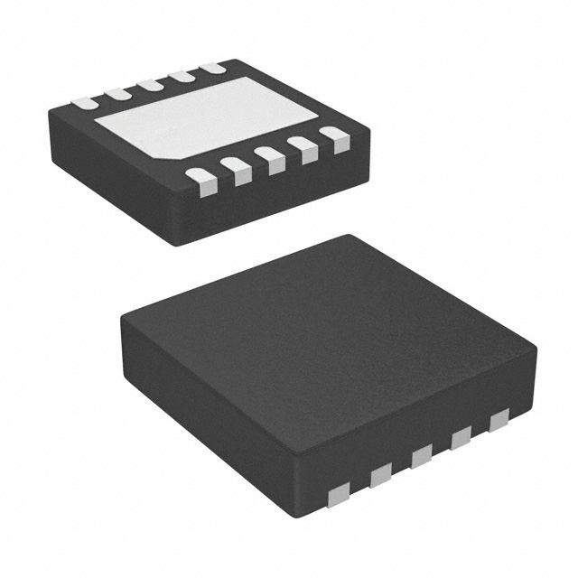


 工商网监
湘ICP备2023018690号
工商网监
湘ICP备2023018690号
