MIC4744
4 MHz Dual 2A Integrated Switch
Buck Regulator
General Description
Features
The Micrel MIC4744 is a high efficiency dual PWM buck
(step-down) regulator that provides dual 2A current output.
The MIC4744 operates at 4MHz. A proprietary internal
compensation technique allows a closed loop bandwidth of
over 200kHz.
•
•
•
•
•
•
•
•
The low on-resistance internal P-Channel MOSFET of the
MIC4744 allows efficiencies over 90%, reduces external
components count and eliminates the need for an
expensive current sense resistor.
The MIC4744 operates from 2.9V to 5.5V input and the
output can be adjusted down to 0.6V. The device can
operate with a maximum duty cycle of 100% for use in lowdropout conditions.
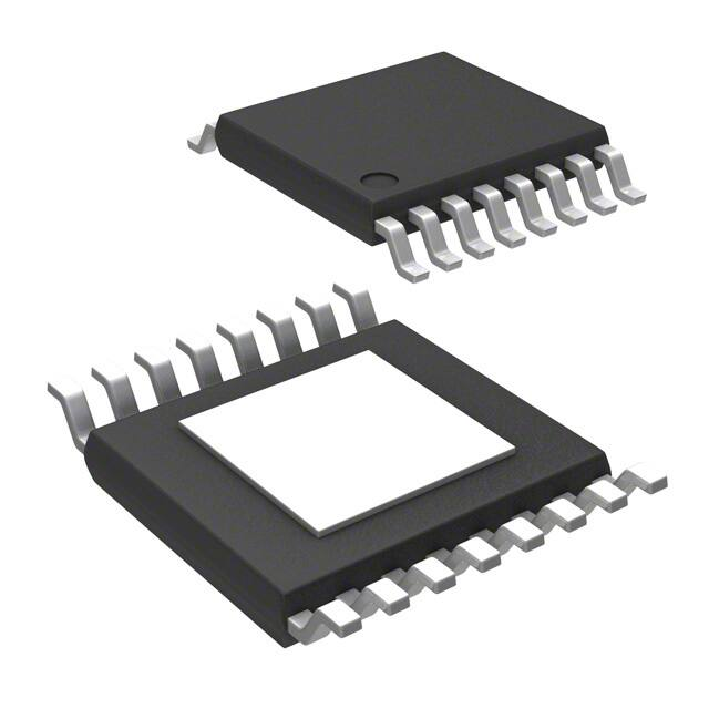
The MIC4744 is available in the exposed pad 16-pin
3mm x 3mm MLF® and ETSSOP-16 packages with
junction operating temperature ranging from –40°C to
+125°C.
All support documentation can be found on Micrel’s web
site at: www.micrel.com.
•
•
•
•
•
2.9 to 5.5V supply voltage
4MHz PWM mode
2A Dual output
Greater than 90% efficiency
100% maximum duty cycle
Output voltage adjustable down to 0.6V
Ultra-fast transient response
Ultra-small external components
Stable with a 0.47µH inductor and a 10µF output
capacitor
Fully integrated 2A MOSFET switches
Micro-power shutdown
Thermal shutdown and current limit protection
Available in 3mm x 3mm 16-pin MLF® and 16-pin
TSSOP packages
–40°C to +125°C junction temperature range
Applications
•
•
•
•
•
•
Broadband: xDSL modems
Automotive satellite radios
HD STB, DVD/TV recorder
Computer peripherals: printers and graphic cards
FPGA/ASIC
General point of load
Typical Application
5.0Vin 3.3Vout Efficiency
100
98
EFFICIENCY (%)
96
94
92
90
88
86
84
82
80
0.0
0.4
0.8
1.2
1.6
2.0
OUTPUT CURRENT (A)
2A 4MHz Dual Buck Regulator
MLF and MicroLeadFrame are registered trademarks of Amkor Technology, Inc.
Micrel Inc. • 2180 Fortune Drive • San Jose, CA 95131 • USA • tel +1 (408) 944-0800 • fax + 1 (408) 474-1000 • http://www.micrel.com
March 2009
1
M9999-030209-C
�Micrel, Inc.
MIC4744
Ordering Information
Output Voltage
Junction Temp. Range
MIC4744YML
Part Number
Adj.
–40° to +125°C
16-Pin 3mm x 3mm MLF®
Package
Lead Finish
Pb-Free
MIC4744YTSE
Adj.
–40° to +125°C
16-Pin EPAD TSSOP
Pb-Free
Note:
®
MLF is a GREEN RoHS-compliant package. Lead finish is NiPdAu. Mold compound is Halogen Free.
Pin Configuration
16-Pin 3mm x 3mm MLF® (YML)
March 2009
16-Pin EPAD-TSSOP (YTSE)
2
M9999-030209-C
�Micrel, Inc.
MIC4744
Pin Description
Pin Number
®
(MLF )
Pin Number
(EPAD-TSSOP)
Pin Name
1
7
FB2
Feedback for output 2 (Input). Input to the error amplifier, connect to the
external resistor divider network to set the output voltage.
2(1)
8(1)
EN2
Enable for output 2 (Input). Logic level low, will shutdown the device, reducing
the current draw to less than 5µA (both EN1 and EN2 are low).
3,4
9,10
SW2
Switch for output 2 (Output): Internal power P-Channel MOSFET output switch
5
11
PGND2
Pin Function
Power Ground for output 2. Provides the ground return path for the high-side
drive current.
PGND1 pin and PGND2 pin are internally connected by anti-parallel diodes.
6,15
5,12
VIN2
Supply Voltage for output 2 (Input): Supply voltage for the source of the
internal P-Channel MOSFET and driver. Requires bypass capacitor to GND.
VIN1 pins and VIN2 pins are internally connected by anti-parallel diodes.
7,14
4,13
VIN1
Supply Voltage for output 1 (Input): Supply voltage for the source of the
internal P-Channel MOSFET and driver. Requires bypass capacitor to GND.
VIN1 pins and VIN2 pins are internally connected by anti-parallel diodes.
8
14
PGND1
Power Ground for output 1. Provides the ground return path for the
high-side drive current.
PGND1 pin and PGND2 pin are internally connected by anti-parallel diodes.
9,10
15,16
SW1
Switch for output 1 (Output): Internal power P-Channel MOSFET output switch
11(1)
1(1)
EN1
Enable for output 1 (Input). Logic level low, will shutdown the device, reducing
the current draw to less than 5µA (both EN1 and EN2 are low).
12
2
FB1
Feedback for output 1 (Input). Input to the error amplifier, connect to the
external resistor divider network to set the output voltage.
13
3
SGND
Signal (Analog) Ground. Provides return path for control circuitry and internal
reference.
16
6
BIAS
Internal circuit bias supply. Must be bypassed with a 0.1µF ceramic capacitor
to SGND. Biased through a 10Ω resistor to VIN.
EPAD
EPAD
GND
Connect to ground.
Note:
1. Do not float Enable Input.
March 2009
3
M9999-030209-C
�Micrel, Inc.
MIC4744
Absolute Maximum Ratings(1)
Operating Ratings(2)
Supply Voltage (VIN) ......................................... -0.3V to +6V
Output Switch Voltage (VSW1, VSW2).................. -0.3V to +6V
Output Switch Current (ISW1, ISW2)………...Internally Limited
Input Voltage (VEN), (VFB), (VBIAS) ...................... -0.3V to VIN
Storage Temperature (Ts) .........................–60°C to +150°C
Junction Temperature ................................................ 150°C
Lead Temperature (soldering, 10sec.)....................... 260°C
ESD Rating(3) ................................................................. 2KV
Supply Voltage (VIN)..................................... +2.9V to +5.5V
Logic Input Voltage (VEN) ....................................... 0V to VIN
Junction Temperature (TJ) ........................ –40°C to +125°C
Junction Thermal Resistance
MLF® (θJA)..........................................................60°C/W
EPAD TSSOP (θJA)............................................35°C/W
Electrical Characteristics(4)
VIN = VEN = 3.6V; L = 1.0µH; COUT = 4.7µF; TA = 25°C, unless noted. Bold values indicate –40°C< TJ < +125°C.
Parameter
Condition
Min
2.9
Supply Voltage Range
Under-Voltage Lockout Threshold
2.45
Turn-on
UVLO Hysteresis
Quiescent Current
Typ
2.6
Max
Units
5.5
V
2.7
100
VFB = 0.9 * VNOM (not switching); VIN = 5.5V
1.4
V
mV
3.0
mA
VFB = 0.9 * VNOM (not switching); VIN = 3.6V
1.0
Shutdown Current
VEN = 0V
1.6
10
µA
[Adjustable] Feedback Voltage
± 2% (over temperature) ILOAD = 100µA
0.6
0.612
V
0.588
FB pin input current
mA
1
2.5
nA
Current Limit
VFB = 0.9 * VNOM
4.3
A
Output Voltage Line Regulation
VIN = 2.9V to 5.5V; ILOAD= 100µA
0.07
%
Output Voltage Load Regulation
20mA < ILOAD < 2A
0.2
%
Maximum Duty Cycle
VFB ≤ 0.9 * VNOM
Switch ON-Resistance
ISW = 50mA VFB =GND
100
%
155
3.0
Oscillator Frequency
Switching Phase
3.8
mΩ
4.4
180
0.5
Enable Threshold
Enable Hysteresis
0.9
MHz
°C
1.3
55
V
mV
2
Enable Input Current
0.1
Over-Temperature Shutdown
153
µA
°C
Over-Temperature Hysteresis
18
°C
Notes:
1. Exceeding the absolute maximum rating may damage the device.
2. The device is not guaranteed to function outside its operating rating.
3. Devices are ESD sensitive. Handling precautions recommended. Human body model, 1.5k in series with 100pF.
4. Specification for packaged product only.
March 2009
4
M9999-030209-C
�Micrel, Inc.
MIC4744
Typical Characteristics
5.0Vin 1.0Vout Efficiency
74
74
78
72
72
76
70
68
66
64
62
3.0Vin
3.3Vin
58
EFFICIENCY (%)
80
60
70
68
66
64
62
60
4.5Vin
58
5.0Vin
3.6Vin
0.4
0.8
1.2
1.6
0.4
OUTPUT CURRENT (A)
68
66
0.8
1.2
1.6
3.3Vin 1.5Vout Efficiency
80
72
70
68
66
4.5Vin
64
78
76
74
72
70
76
74
72
2
0
0.4
0.8
1.2
1.6
2
0
86
92
84
84
90
82
82
88
76
74
72
70
EFFICIENCY (%)
86
EFFICIENCY (%)
94
78
80
78
76
74
3.0Vin
72
3.3Vin
70
4.5Vin
5.0Vin
3.6Vin
0.4
94
90
92
88
90
86
84
82
80
0.8
1.2
1.6
0
0.4
80
78
4.5Vin
1.6
2
1.005
1.000
0.995
Vin=3.3V
5.5Vin
76
2.0
1.2
5.0Vin
5.5Vin
74
0.8
Load Regulation
82
5.0Vin
March 2009
3.3Vin
1.010
84
76
OUTPUT CURRENT (A)
3.0Vin
76
OUTPUT CURRENT (A)
86
4.5Vin
1.6
78
2
88
78
1.2
80
OUTPUT VOLTAGE (V)
92
0.8
82
5.0Vin 3.3Vout Efficiency
96
EFFICIENCY (%)
EFFICIENCY (%)
5.0Vin 2.5Vout Efficiency
94
0.4
84
OUTPUT CURRENT (A)
OUTPUT CURRENT (A)
0.0
86
74
0
2
2
3.6Vin
68
1.6
1.6
5.5Vin
68
1.2
1.2
3.3Vin 2.5Vout Efficiency
88
80
0.8
OUTPUT CURRENT (A)
5.0Vin 1.8Vout Efficiency
3.3Vin 1.8Vout Efficiency
0.8
0.4
OUTPUT CURRENT (A)
88
0.4
5.0Vin
64
OUTPUT CURRENT (A)
0
4.5Vin
5.5Vin
64
1.6
2
78
66
3.6Vin
60
1.6
68
3.3Vin
66
5.5Vin
1.2
70
3.0Vin
68
5.0Vin
62
EFFICIENCY (%)
82
80
EFFICIENCY (%)
82
76
74
0.8
5.0Vin 1.5Vout Efficiency
78
1.2
0.4
OUTPUT CURRENT (A)
84
0.8
3.6Vin
0
84
0.4
3.3Vin
2
80
0
3.0Vin
OUTPUT CURRENT (A)
5.0Vin 1.2Vout Efficiency
EFFICIENCY (%)
70
60
0
2
72
62
56
0
74
64
5.5Vin
56
EFFICIENCY (%)
3.3Vin 1.2Vout Efficiency
76
EFFICIENCY (%)
EFFICIENCY (%)
3.3Vin 1.0Vout Efficiency
76
0.990
0.0
0.4
0.8
1.2
1.6
OUTPUT CURRENT (A)
5
2.0
0
0.4
0.8
1.2
1.6
2
OUTPUT CURRENT (A)
M9999-030209-C
�Micrel, Inc.
MIC4744
Typical Characteristics (continue)
Feedback Voltage
vs. Temperature
Frequency
vs. Temperature
1.0030
0.605
1.0028
0.604
4.2
1.0026
0.603
4.1
1.0024
1.0022
1.0020
1.0018
1.0016
1.0014
4.3
FREQUENCY (MHz)
FEEDBACK VOLTAGE (V)
OUTPUT VOLTAGE (V)
Line Regulation
0.602
0.601
0.600
0.599
0.598
4.0
3.9
3.8
3.7
3.6
0.597
3.5
1.0012
0.596
3.4
1.0010
0.595
2.9
3.3
3.7
4.1
4.5
4.9
5.3
3.3
-40
-20
0
SUPPLY VOLTAGE (V)
20
40
60
80
100
120
-40
-20
TEMPERATURE (°C)
Feedback Voltage
vs. Supply Voltage
20
40
60
80
100
120
TEMPERATURE (°C)
Quiescent Current
vs. Supply Voltage
0.8
0
Rdson
vs. Supply Voltage
1600
180
0.4
0.2
1200
160
Rdson (mΩ)
QUIESCENT CURRENT (μA)
FEEDBACK VOLTAGE (V)
170
0.6
800
2
3
4
5
100
0
1
SUPPLY VOLTAGE (V)
2
3
4
2.9
5
1.2
1.2
1.0
1.0
140
130
120
110
ENABLE THRESHOLD (V)
ENABLE THRESHOLD (V)
Rdson (mΩ)
150
0.8
0.6
0.4
0.2
0.0
100
0
20
40
60
TEMPERATURE (°C)
March 2009
80
100
120
4.1
4.5
4.9
5.3
Enable Threshold
vs. Temperature
170
160
3.7
SUPPLY VOLTAGE (V)
Enable Threshold
vs. Supply Voltage
180
-20
3.3
SUPPLY VOLTAGE (V)
Rdson
vs. Temperature
-40
130
110
0
1
140
120
400
0.0
0
150
0.8
0.6
0.4
0.2
0.0
2.9
3.3
3.7
4.1
4.5
4.9
SUPPLY VOLTAGE (V)
6
5.3
-40
-20
0
20
40
60
80
100
120
TEMPERATURE (°C)
M9999-030209-C
�Micrel, Inc.
MIC4744
Functional Characteristics
March 2009
7
M9999-030209-C
�Micrel, Inc.
MIC4744
Functional Diagram
MIC4744 Block Diagram
March 2009
8
M9999-030209-C
�Micrel, Inc.
MIC4744
Pin Description
SW1/SW2
The switch pins (SW1 and SW2) connect directly to the
inductor and provide the switching current necessary to
operate in PWM mode. Due to the high speed switching
on these pins, the switch nodes should be routed away
from sensitive nodes. These pins also connect to the
cathodes of the free-wheeling diodes.
VIN1/VIN2
VIN pins (two pins for VIN1 and two pins for VIN2)
provide power to the source of the internal P-Channel
MOSFET along with the current limiting sensing. VIN1
pins and VIN2 pins are internally connected by antiparallel diodes. The VIN operating voltage range is from
2.9V to 5.5V. Due to the high switching speeds, a 10µF
capacitor is recommended close to VIN and the power
ground (PGND) for each pin for bypassing. Please refer
to layout recommendations for more details.
PGND1/PGND2
Power ground pins (PGND1 and PGND2) are the ground
paths for the MOSFET drive current. PGND1 pin and
PGND2 pin are internally connected by anti-parallel
diodes. The current loop for the power ground should be
as small as possible and separate from the Signal
ground (SGND)
loop.
Refer
to
the
layout
recommendation for more details.
BIAS
The bias (BIAS) provides power to the internal reference
and control sections of the MIC4744. A 10Ω resistor
from VIN to BIAS and a 0.1µF from BIAS to SGND are
required for clean operation.
SGND
Signal ground (SGND) is the ground path for the biasing
and control circuitry. The current loop for the signal
ground should be separate from the power ground
(PGND) loop. Refer to the layout recommendation for
more details.
EN1/EN2
The enable pins (EN1 and EN2) provides a logic level
control of the outputs 1 and 2. In the off state, supply
current of the device is greatly reduced (typically
很抱歉,暂时无法提供与“MIC4744YTSE”相匹配的价格&库存,您可以联系我们找货
免费人工找货- 国内价格 香港价格
- 376+11.75911376+1.52421