MIC5249
300 mA µCap LDO with Programmable Power-On Reset Delay
Features
General Description
•
•
•
•
The MIC5249 is an efficient, precise 300 mA CMOS
voltage regulator with power on reset (POR) delay
which can be implemented via an external capacitor. It
offers 1% initial accuracy, extremely low dropout
voltage (typically 400 mV @ 300 mA), and low ground
current (typically 85 mA) over load.
•
•
•
•
•
•
300 mA Output Current
High PSRR: 65 dB@120 Hz
Stable with Ceramic Output Capacitor
Power-on-Reset (POR) Output with Adjustable
Delay Time
High Output Accuracy:
- ±1.0% Initial Accuracy
- ±3.0% Over Temperature
Low Dropout Voltage of 340 mV @ 300 mA
Low Quiescent Current: 85 µA
Zero Current Shutdown Mode
Thermal Shutdown and Current-Limit Protection
Tiny MSOP-8 Package
Applications
• Cellular Phones
• PDAs
• Fiber Optic Modules
Designed specifically for noise-critical applications in
hand-held or battery-powered devices, the MIC5249
comes equipped with a noise reduction feature to filter
the output noise via an external capacitor. Other
features of the MIC5249 include a logic-compatible
enable pin, current limit, thermal shutdown, ultra-fast
transient response, and an active clamp to speed up
device turnoff.
The MIC5249 also works with low-ESR ceramic
capacitors, reducing the amount of board space
necessary for power applications, critical in hand-held
wireless devices.
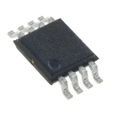
The MIC5249 is available in the MSOP-8 package.
Package Type
MIC5249
8-Lead MSOP (MM)
(Top View)
CBYP 1
DELAY 2
GND 3
VIN 4
2021 Microchip Technology Inc. and its subsidiaries
8 ENABLE
7 RESET
6 NC
5 VOUT
DS20006602A-page 1
�MIC5249
Typical Application Circuit
Ultra-Low Noise Application
Functional Block Diagram
DS20006602A-page 2
2021 Microchip Technology Inc. and its subsidiaries
�MIC5249
1.0
ELECTRICAL CHARACTERISTICS
Absolute Maximum Ratings †
Supply Voltage (VIN) ......................................................................................................................................... 0V to +7V
Enable Input Voltage (VEN) ............................................................................................................................... 0V to +7V
Power Dissipation (PD), Note 1.............................................................................................................. Internally Limited
ESD Rating, Note 2.................................................................................................................................... ESD Sensitive
Operating Ratings ‡
Supply Voltage (VIN) .................................................................................................................................... +2.7V to +6V
Enable Input Voltage (VEN) .................................................................................................................................0V to VIN
† Notice: Stresses above those listed under “Absolute Maximum Ratings” may cause permanent damage to the device.
This is a stress rating only and functional operation of the device at those or any other conditions above those indicated
in the operational sections of this specification is not intended. Exposure to maximum rating conditions for extended
periods may affect device reliability.
‡ Notice: The device is not guaranteed to function outside its operating ratings.
Note 1: The maximum allowable power dissipation of any TA (ambient temperature) is PD(MAX) = (TJ(MAX) – TA)/θJA.
Exceeding the maximum allowable power dissipation will result in excessive die temperature, and the
regulator will go into thermal shutdown.
2: Devices are ESD sensitive. Handling precautions are recommended. Human body model, 1.5 kΩ in series
with 100 pF.
ELECTRICAL CHARACTERISTICS
Electrical Characteristics: VIN = VOUT + 1V; IOUT = 100 µA; TJ = +25°C;
Bold values indicate –40°C to +125°C unless noted.
Parameters
Symbol
Min.
Typ.
Max.
–1.0
—
+1.0
–3.0
—
+3.0
Units
Output Voltage
Accuracy
VOUT
Line Regulation
ΔVOUT/
(VOUT x ΔVIN)
–0.3
0.02
+0.3
%/V
Load Regulation
ΔVOUT/VOUT
—
1.5
3.0
%
—
1
—
—
160
225
275
—
340
500
600
Dropout Voltage
VDO
85
150
100
200
0.35
1
—
65
—
300
440
—
Ground Pin Current
IGND
Ground Pin Current
in Shutdown
ISHDN
Ripple Rejection
PSRR
ILIM
VIL
—
—
VIH
1.6
—
—
IIL
—
0.01
—
IIH
—
0.01
—
Current Limit
—
%
Enable Input Current
2021 Microchip Technology Inc. and its subsidiaries
0.4
Variation from nominal VOUT
VIN = VOUT + 1V to 6V
IOUT = 0.1 mA to 300 mA
IOUT = 100 µA
mV
IOUT = 150 mA
IOUT = 300 mA
µA
µA
IOUT = 0 mA
IOUT = 300 mA
VEN < 0.4V (Regulator OFF)
dB
f = 120 Hz; COUT = 2.2 µF
mA
VOUT = 0V
Enable Input
Enable Input Voltage
Conditions
V
µA
Logic low (regulator shutdown)
Logic high (regulator enabled)
VIL < 0.4V (regulator shutdown)
VIH > 1.6V (regulator enabled)
DS20006602A-page 3
�MIC5249
ELECTRICAL CHARACTERISTICS (CONTINUED)
Electrical Characteristics: VIN = VOUT + 1V; IOUT = 100 µA; TJ = +25°C;
Bold values indicate –40°C to +125°C unless noted.
Parameters
Symbol
Min.
Typ.
Max.
Units
Conditions
Delay Pin Current
Source
IDELAY_TH
—
0.55
1
µA
—
Delay Pin Threshold
Voltage
VDELAY_TH
—
1.4
—
V
Threshold for RESET = Logic high
—
Delay Input
RESET Output
VTHL
89
91
Reset High
Threshold
VTHH
—
93
96
Reset Output
Logic-Low Voltage
VOL
—
0.02
0.1
V
IRESET = 100 µA output in fault condition
IRESET
—
0.01
—
µA
Flag OFF
Reset Low Threshold
Flag Leakage
Current
% of VOUT (Flag ON)
%
% of VOUT (Flag OFF)
TEMPERATURE SPECIFICATIONS
Parameters
Symbol
Min.
Typ.
Max.
Units
Conditions
Junction Temperature Range
TJ
–40
—
+125
°C
Storage Temperature Range
TS
–65
—
+150
°C
—
Lead Temperature
—
—
—
+260
°C
Soldering, 5 sec.
JA
—
160
—
°C/W
Temperature Ranges
Note 1
Package Thermal Resistances
Thermal Resistance, MSOP-8
Note 1:
—
The maximum allowable power dissipation is a function of ambient temperature, the maximum allowable
junction temperature and the thermal resistance from junction to air (i.e., TA, TJ, JA). Exceeding the
maximum allowable power dissipation will cause the device operating junction temperature to exceed the
maximum +125°C rating. Sustained junction temperatures above +125°C can impact the device reliability.
DS20006602A-page 4
2021 Microchip Technology Inc. and its subsidiaries
�MIC5249
2.0
PIN DESCRIPTIONS
The descriptions of the pins are listed in Table 2-1.
TABLE 2-1:
PIN FUNCTION TABLE
Pin Number
Pin Name
Description
1
CBYP
Reference Bypass. Connect external 0.01µF capacitor to GND to reduce output noise.
May be left open.
2
DELAY
Delay Set Input. Connect external capacitor to GND to set the delay of the Error Flag.
3
GND
4
VIN
5
VOUT
6
NC
7
RESET
8
ENABLE
Ground.
Supply input.
Regulator output.
No connect.
RESET Output. Open-drain output. Active low indicates an output undervoltage
condition.
Enable Input: CMOS-compatible input. Logic high = enable; Logic low = shutdown. Do
not leave open.
2021 Microchip Technology Inc. and its subsidiaries
DS20006602A-page 5
�MIC5249
3.0
APPLICATION INFORMATION
3.1
Enable/Shutdown
The MIC5249 comes with an active-high enable pin
that allows the regulator to be disabled. Forcing the
enable pin low disables the regulator and sends it into
a “zero” off-mode-current state. In this state, current
consumed by the regulator goes nearly to zero. Forcing
the enable pin high enables the output voltage. This
part is CMOS and the enable pin cannot be left floating;
a floating enable pin may cause an indeterminate state
on the output.
3.2
Input Capacitor
The MIC5249 is a high-performance, high-bandwidth
device. Therefore, it requires a well-bypassed input
supply for optimal performance. A 1.0 µF capacitor is
required from the input to ground to provide stability.
Low-ESR ceramic capacitors provide optimal
performance at a minimum of space. Additional
high-frequency capacitors such as small valued NPO
dielectric type capacitors help to filter out high
frequency noise and are good practice in any
RF-based circuit.
3.3
Output Capacitor
The MIC5249 requires an output capacitor of 2.2 µF or
greater to maintain stability. The design is optimized for
use with low-ESR ceramic chip capacitors. High-ESR
capacitors may cause high frequency oscillation. The
maximum recommended ESR is 300 mΩ. The output
capacitor can be increased, but performance has been
optimized for a 2.2 µF ceramic output capacitor and
does not improve significantly with larger capacitance.
X7R/X5R dielectric-type ceramic capacitors are
recommended because of their temperature
performance. X7R-type capacitors change capacitance
by 15% over their operating temperature range and are
the most stable type of ceramic capacitors. Z5U and
Y5V dielectric capacitors change value by as much as
50% and 60%, respectively, over their operating
temperature ranges. To use a ceramic chip capacitor
with Y5V dielectric, the value must be much higher than
anX7R ceramic capacitor to ensure the same minimum
capacitance over the equivalent operating temperature
range.
3.4
DELAY Pin Input
The power-on-reset (POR) function can be
implemented on the MIC5249 by adding an external
capacitor from the DELAY pin to ground. This external
capacitor sets the delay time (tDELAY) of the RESET
output.
DS20006602A-page 6
The capacitor value required can be easily calculated
using the formula:
EQUATION 3-1:
T DELAY I DELAY
C DELAY = -------------------------------------------
V DELAY
Where:
IDELAY =
0.55 µA
VDELAY =
1.4V
When no capacitor is used, there will be no delay and
the POR output acts like a standard error FLAG output.
3.5
RESET Output
The RESET output of the MIC5249 provides the
power-on reset signal based on the capacitor from the
DELAY pin to ground when input power is applied to the
regulator. The reset signal stays low for a preset time
period after power is applied to the regulator, and then
goes high.
The reset output is an active-low, open-drain output
that drives low when a fault condition AND an
undervoltage detection occurs. Internal circuitry
intelligently monitors overcurrent, overtemperature and
dropout conditions and ORs these outputs together to
indicate some fault condition. The output of that OR
gate is ANDed with an output voltage monitor that
detects an undervoltage condition. The output drives
an open-drain transistor to indicate a fault. This
prevents chattering or inadvertent triggering of the
reset. There set must be pulled up using a resistor form
the RESET pin to either the input or the output.
3.6
Bypass Pin Output
A bypass capacitor is required from the noise bypass
pin to ground to reduce output voltage noise. The
capacitor bypasses the internal reference. A 0.01 µF
capacitor is recommended for applications that require
low-noise outputs. The bypass capacitor can be
increased, further reducing noise and improving
PSRR. Turn-on time increases slightly with respect to
bypass capacitance. A unique quick-start circuit allows
the MIC5249 to drive a large capacitor on the bypass
pin without significantly slowing the turn-on time.
3.7
Active Shutdown
The MIC5249 also features an active shutdown clamp,
which is a N-Channel MOSFET that turns on when the
device is disabled. This allows the output capacitor and
load to discharge, de-energizing the load.
2021 Microchip Technology Inc. and its subsidiaries
�MIC5249
3.8
No-Load Stability
The MIC5249 will remain stable and in regulation with
no load unlike many other voltage regulators. This is
especially important in CMOS RAM keep-alive
application.
3.9
Thermal Considerations
The MIC5249 is designed to provide 300 mA of
continuous current in a very small package. Maximum
power dissipation can be calculated based on the
output current and the voltage drop across the device.
To determine the maximum power dissipation of the
package, use the junction-to-ambient thermal
resistance of the device and the following basic
equation:
EQUATION 3-2:
Where:
TJ(MAX) =
The maximum junction temperature of
the die, 125°C
TA =
The ambient operating temperature
JA =
Layout independent
Table 3-1 shows examples of the junction-to-ambient
thermal resistance for MIC5249.
MSOP-8 THERMAL
RESISTANCE
Package
P D MAX = 125C – 50C 160C/W
The junction-to-ambient thermal resistance for the
minimum footprint is 160°C/W, from Table 3-1. The
maximum power dissipation must not be exceeded for
proper operation. Using the output voltage of 3.0V, and
an output current of 300 mA, the maximum input
voltage can be determined. Because this device is
CMOS and the ground current is typically 90 µA over
the load range, the power dissipation contributed by the
ground current is < 1.0% and can be ignored for this
calculation:
EQUATION 3-5:
T J MAX – T A
P D MAX = --------------------------------
JA
TABLE 3-1:
EQUATION 3-4:
θJA Recommended
Minimum Footprint
468mW = V IN – 3.0V 300mA
468mW = V IN 300mA – 900mW
1368mW = V IN 300mA
V IN MAX = 4.56V
Therefore, a 3.0V application at 300 mA of output
current can accept a maximum input voltage of 4.56V
in the MSOP-8 package. For a full discussion of heat
sinking and thermal effects on the voltage regulators,
refer to the Regulator Thermals section of Designing
with Low-Dropout Voltage Regulators handbook.
MSOP-8
160°C/W
The actual power dissipation of the regulator circuit can
be determined using the equation:
EQUATION 3-3:
P D = V IN – V OUT I OUT + V IN I GND
Substituting PD(MAX) for PD and solving for the
operating conditions that are critical to the application
will give the maximum operating conditions for the
regulator circuit. For example, when operating the
MIC5249-3.0YMM at 50°C with a minimum footprint
layout, the maximum input voltage for a set output
current can be determined as follows:
2021 Microchip Technology Inc. and its subsidiaries
DS20006602A-page 7
�MIC5249
4.0
PACKAGING INFORMATION
4.1
Package Marking Information
8-Lead MSOP*
Legend: XX...X
Y
YY
WW
NNN
e3
*
Example
XXXX
5249
X.XY
3.3Y
Product code or customer-specific information
Year code (last digit of calendar year)
Year code (last 2 digits of calendar year)
Week code (week of January 1 is week ‘01’)
Alphanumeric traceability code
Pb-free JEDEC® designator for Matte Tin (Sn)
This package is Pb-free. The Pb-free JEDEC designator ( e3 )
can be found on the outer packaging for this package.
●, ▲, ▼ Pin one index is identified by a dot, delta up, or delta down (triangle
mark).
Note:
In the event the full Microchip part number cannot be marked on one line, it will
be carried over to the next line, thus limiting the number of available
characters for customer-specific information. Package may or may not include
the corporate logo.
Underbar (_) and/or Overbar (‾) symbol may not be to scale.
DS20006602A-page 8
2021 Microchip Technology Inc. and its subsidiaries
�MIC5249
8-Lead MSOP Package Outline and Recommended Land Pattern
Note:
For the most current package drawings, please see the Microchip Packaging Specification located at
http://www.microchip.com/packaging.
2021 Microchip Technology Inc. and its subsidiaries
DS20006602A-page 9
�MIC5249
NOTES:
DS20006602A-page 10
2021 Microchip Technology Inc. and its subsidiaries
�MIC5249
APPENDIX A:
REVISION HISTORY
Revision A (October 2021)
• Converted Micrel document MIC5249 to Microchip data sheet DS20006602A.
• Minor text changes throughout.
2021 Microchip Technology Inc. and its subsidiaries
DS20006602A-page 11
�MIC5249
NOTES:
DS20006602A-page 12
2021 Microchip Technology Inc. and its subsidiaries
�MIC5249
PRODUCT IDENTIFICATION SYSTEM
To order or obtain information, e.g., on pricing or delivery, contact your local Microchip representative or sales office.
PART NO.
Device
X
-XX
XX
Package
Junction
Voltage
Option Temperature Range
-XX
Media Type
Device:
MIC5249: 300 mA µCap LDO with Programmable Power-On
Reset Delay
Voltage Option
1.5 = 1.5V
1.8 = 1.8V
2.5 = 2.5V
2.6 = 2.6V
2.8 = 2.8V
2.85 = 2.85V
3.0 = 3.0V
3.3 = 3.3V
Junction
Temperature
Range:
Y
Package:
MM =
Media Type:
=100/Tube
TR
= 2,500/Reel
=
Examples:
a) MIC5249-1.8YMM
300 mA µCap LDO with
Programmable Power-On Reset
Delay, 1.8V, –40°C to +125°C,
8-Lead MSOP, 100/Tube
b) MIC5249-1.8YMM-TR 300 mA µCap LDO with
Programmable Power-On Reset
Delay, 1.8V, –40°C to +125°C,
8-Lead MSOP, 2,500/Reel
c) MIC5249-2.85YMM
300 mA µCap LDO with
Programmable Power-On Reset
Delay, 2.85V, –40°C to +125°C,
8-Lead MSOP, 100/Tube
c) MIC5249-2.85YMMTR
300 mA µCap LDO with
Programmable Power-On Reset
Delay, 2.85V, –40°C to +125°C,
8-Lead MSOP, 2,500/Reel
–40°C to +125°C
Note 1:
8-Lead MSOP (Pb-Free)
2021 Microchip Technology Inc. and its subsidiaries
Tape and Reel identifier only appears in the
catalog part number description. This identifier is
used for ordering purposes and is not printed on
the device package. Check with your Microchip
Sales Office for package availability with the
Tape and Reel option.
DS20006602A-page 13
�MIC5249
NOTES:
DS20006602A-page 14
2021 Microchip Technology Inc. and its subsidiaries
�Note the following details of the code protection feature on Microchip products:
•
Microchip products meet the specifications contained in their particular Microchip Data Sheet.
•
Microchip believes that its family of products is secure when used in the intended manner, within operating specifications, and
under normal conditions.
•
Microchip values and aggressively protects its intellectual property rights. Attempts to breach the code protection features of
Microchip product is strictly prohibited and may violate the Digital Millennium Copyright Act.
•
Neither Microchip nor any other semiconductor manufacturer can guarantee the security of its code. Code protection does not
mean that we are guaranteeing the product is “unbreakable”. Code protection is constantly evolving. Microchip is committed to
continuously improving the code protection features of our products.
This publication and the information herein may be used only
with Microchip products, including to design, test, and integrate
Microchip products with your application. Use of this information in any other manner violates these terms. Information
regarding device applications is provided only for your convenience and may be superseded by updates. It is your responsibility to ensure that your application meets with your
specifications. Contact your local Microchip sales office for
additional support or, obtain additional support at https://
www.microchip.com/en-us/support/design-help/client-supportservices.
THIS INFORMATION IS PROVIDED BY MICROCHIP "AS IS".
MICROCHIP MAKES NO REPRESENTATIONS OR WARRANTIES OF ANY KIND WHETHER EXPRESS OR IMPLIED,
WRITTEN OR ORAL, STATUTORY OR OTHERWISE,
RELATED TO THE INFORMATION INCLUDING BUT NOT
LIMITED TO ANY IMPLIED WARRANTIES OF NONINFRINGEMENT, MERCHANTABILITY, AND FITNESS FOR A
PARTICULAR PURPOSE, OR WARRANTIES RELATED TO
ITS CONDITION, QUALITY, OR PERFORMANCE.
IN NO EVENT WILL MICROCHIP BE LIABLE FOR ANY INDIRECT, SPECIAL, PUNITIVE, INCIDENTAL, OR CONSEQUENTIAL LOSS, DAMAGE, COST, OR EXPENSE OF ANY
KIND WHATSOEVER RELATED TO THE INFORMATION OR
ITS USE, HOWEVER CAUSED, EVEN IF MICROCHIP HAS
BEEN ADVISED OF THE POSSIBILITY OR THE DAMAGES
ARE FORESEEABLE. TO THE FULLEST EXTENT
ALLOWED BY LAW, MICROCHIP'S TOTAL LIABILITY ON
ALL CLAIMS IN ANY WAY RELATED TO THE INFORMATION
OR ITS USE WILL NOT EXCEED THE AMOUNT OF FEES, IF
ANY, THAT YOU HAVE PAID DIRECTLY TO MICROCHIP
FOR THE INFORMATION.
Use of Microchip devices in life support and/or safety applications is entirely at the buyer's risk, and the buyer agrees to
defend, indemnify and hold harmless Microchip from any and
all damages, claims, suits, or expenses resulting from such
use. No licenses are conveyed, implicitly or otherwise, under
any Microchip intellectual property rights unless otherwise
stated.
Trademarks
The Microchip name and logo, the Microchip logo, Adaptec,
AnyRate, AVR, AVR logo, AVR Freaks, BesTime, BitCloud,
CryptoMemory, CryptoRF, dsPIC, flexPWR, HELDO, IGLOO,
JukeBlox, KeeLoq, Kleer, LANCheck, LinkMD, maXStylus,
maXTouch, MediaLB, megaAVR, Microsemi, Microsemi logo,
MOST, MOST logo, MPLAB, OptoLyzer, PIC, picoPower,
PICSTART, PIC32 logo, PolarFire, Prochip Designer, QTouch,
SAM-BA, SenGenuity, SpyNIC, SST, SST Logo, SuperFlash,
Symmetricom, SyncServer, Tachyon, TimeSource, tinyAVR, UNI/O,
Vectron, and XMEGA are registered trademarks of Microchip
Technology Incorporated in the U.S.A. and other countries.
AgileSwitch, APT, ClockWorks, The Embedded Control Solutions
Company, EtherSynch, Flashtec, Hyper Speed Control, HyperLight
Load, IntelliMOS, Libero, motorBench, mTouch, Powermite 3,
Precision Edge, ProASIC, ProASIC Plus, ProASIC Plus logo, QuietWire, SmartFusion, SyncWorld, Temux, TimeCesium, TimeHub,
TimePictra, TimeProvider, TrueTime, WinPath, and ZL are
registered trademarks of Microchip Technology Incorporated in the
U.S.A.
Adjacent Key Suppression, AKS, Analog-for-the-Digital Age, Any
Capacitor, AnyIn, AnyOut, Augmented Switching, BlueSky,
BodyCom, CodeGuard, CryptoAuthentication, CryptoAutomotive,
CryptoCompanion, CryptoController, dsPICDEM, dsPICDEM.net,
Dynamic Average Matching, DAM, ECAN, Espresso T1S,
EtherGREEN, GridTime, IdealBridge, In-Circuit Serial
Programming, ICSP, INICnet, Intelligent Paralleling, Inter-Chip
Connectivity, JitterBlocker, Knob-on-Display, maxCrypto, maxView,
memBrain, Mindi, MiWi, MPASM, MPF, MPLAB Certified logo,
MPLIB, MPLINK, MultiTRAK, NetDetach, NVM Express, NVMe,
Omniscient Code Generation, PICDEM, PICDEM.net, PICkit,
PICtail, PowerSmart, PureSilicon, QMatrix, REAL ICE, Ripple
Blocker, RTAX, RTG4, SAM-ICE, Serial Quad I/O, simpleMAP,
SimpliPHY, SmartBuffer, SmartHLS, SMART-I.S., storClad, SQI,
SuperSwitcher, SuperSwitcher II, Switchtec, SynchroPHY, Total
Endurance, TSHARC, USBCheck, VariSense, VectorBlox, VeriPHY,
ViewSpan, WiperLock, XpressConnect, and ZENA are trademarks
of Microchip Technology Incorporated in the U.S.A. and other
countries.
SQTP is a service mark of Microchip Technology Incorporated in
the U.S.A.
The Adaptec logo, Frequency on Demand, Silicon Storage
Technology, Symmcom, and Trusted Time are registered
trademarks of Microchip Technology Inc. in other countries.
GestIC is a registered trademark of Microchip Technology Germany
II GmbH & Co. KG, a subsidiary of Microchip Technology Inc., in
other countries.
All other trademarks mentioned herein are property of their
respective companies.
© 2021, Microchip Technology Incorporated and its subsidiaries.
All Rights Reserved.
For information regarding Microchip’s Quality Management Systems,
please visit www.microchip.com/quality.
2021 Microchip Technology Inc. and its subsidiaries
ISBN: 978-1-5224-9213-9
DS20006602A-page 15
�Worldwide Sales and Service
AMERICAS
ASIA/PACIFIC
ASIA/PACIFIC
EUROPE
Corporate Office
2355 West Chandler Blvd.
Chandler, AZ 85224-6199
Tel: 480-792-7200
Fax: 480-792-7277
Technical Support:
http://www.microchip.com/
support
Web Address:
www.microchip.com
Australia - Sydney
Tel: 61-2-9868-6733
India - Bangalore
Tel: 91-80-3090-4444
China - Beijing
Tel: 86-10-8569-7000
India - New Delhi
Tel: 91-11-4160-8631
Austria - Wels
Tel: 43-7242-2244-39
Fax: 43-7242-2244-393
China - Chengdu
Tel: 86-28-8665-5511
India - Pune
Tel: 91-20-4121-0141
China - Chongqing
Tel: 86-23-8980-9588
Japan - Osaka
Tel: 81-6-6152-7160
China - Dongguan
Tel: 86-769-8702-9880
Japan - Tokyo
Tel: 81-3-6880- 3770
China - Guangzhou
Tel: 86-20-8755-8029
Korea - Daegu
Tel: 82-53-744-4301
China - Hangzhou
Tel: 86-571-8792-8115
Korea - Seoul
Tel: 82-2-554-7200
China - Hong Kong SAR
Tel: 852-2943-5100
Malaysia - Kuala Lumpur
Tel: 60-3-7651-7906
China - Nanjing
Tel: 86-25-8473-2460
Malaysia - Penang
Tel: 60-4-227-8870
China - Qingdao
Tel: 86-532-8502-7355
Philippines - Manila
Tel: 63-2-634-9065
China - Shanghai
Tel: 86-21-3326-8000
Singapore
Tel: 65-6334-8870
China - Shenyang
Tel: 86-24-2334-2829
Taiwan - Hsin Chu
Tel: 886-3-577-8366
China - Shenzhen
Tel: 86-755-8864-2200
Taiwan - Kaohsiung
Tel: 886-7-213-7830
China - Suzhou
Tel: 86-186-6233-1526
Taiwan - Taipei
Tel: 886-2-2508-8600
China - Wuhan
Tel: 86-27-5980-5300
Thailand - Bangkok
Tel: 66-2-694-1351
China - Xian
Tel: 86-29-8833-7252
Vietnam - Ho Chi Minh
Tel: 84-28-5448-2100
Atlanta
Duluth, GA
Tel: 678-957-9614
Fax: 678-957-1455
Austin, TX
Tel: 512-257-3370
Boston
Westborough, MA
Tel: 774-760-0087
Fax: 774-760-0088
Chicago
Itasca, IL
Tel: 630-285-0071
Fax: 630-285-0075
Dallas
Addison, TX
Tel: 972-818-7423
Fax: 972-818-2924
Detroit
Novi, MI
Tel: 248-848-4000
Houston, TX
Tel: 281-894-5983
Indianapolis
Noblesville, IN
Tel: 317-773-8323
Fax: 317-773-5453
Tel: 317-536-2380
Los Angeles
Mission Viejo, CA
Tel: 949-462-9523
Fax: 949-462-9608
Tel: 951-273-7800
Raleigh, NC
Tel: 919-844-7510
New York, NY
Tel: 631-435-6000
San Jose, CA
Tel: 408-735-9110
Tel: 408-436-4270
Canada - Toronto
Tel: 905-695-1980
Fax: 905-695-2078
DS20006602A-page 16
China - Xiamen
Tel: 86-592-2388138
China - Zhuhai
Tel: 86-756-3210040
Denmark - Copenhagen
Tel: 45-4485-5910
Fax: 45-4485-2829
Finland - Espoo
Tel: 358-9-4520-820
France - Paris
Tel: 33-1-69-53-63-20
Fax: 33-1-69-30-90-79
Germany - Garching
Tel: 49-8931-9700
Germany - Haan
Tel: 49-2129-3766400
Germany - Heilbronn
Tel: 49-7131-72400
Germany - Karlsruhe
Tel: 49-721-625370
Germany - Munich
Tel: 49-89-627-144-0
Fax: 49-89-627-144-44
Germany - Rosenheim
Tel: 49-8031-354-560
Israel - Ra’anana
Tel: 972-9-744-7705
Italy - Milan
Tel: 39-0331-742611
Fax: 39-0331-466781
Italy - Padova
Tel: 39-049-7625286
Netherlands - Drunen
Tel: 31-416-690399
Fax: 31-416-690340
Norway - Trondheim
Tel: 47-7288-4388
Poland - Warsaw
Tel: 48-22-3325737
Romania - Bucharest
Tel: 40-21-407-87-50
Spain - Madrid
Tel: 34-91-708-08-90
Fax: 34-91-708-08-91
Sweden - Gothenberg
Tel: 46-31-704-60-40
Sweden - Stockholm
Tel: 46-8-5090-4654
UK - Wokingham
Tel: 44-118-921-5800
Fax: 44-118-921-5820
2021 Microchip Technology Inc. and its subsidiaries
09/14/21
�


 工商网监
湘ICP备2023018690号
工商网监
湘ICP备2023018690号
