MIC5303
Single 300mA CMOS
Ultra Small ULDO™
General Description
Features
The MIC5303 is an ultra small, Ultra Low Dropout CMOS
regulator, ULDO™ that is ideal for today’s most demanding portable applications including cellular phone RF
power, camera modules, imaging sensors for digital still
and video cameras, PDAs, portable media players (PMP)
and PC cameras where board space is limited. It offers
extremely low dropout voltage, very low output noise and
can operate from a 2.3V to 5.5V input while delivering up
to 300mA.
It offers 2% initial accuracy, low ground current (typically
85µA total), thermal and current limit protection. The
MIC5303 can also be put into a zero-off-mode current
state, drawing no current when disabled.
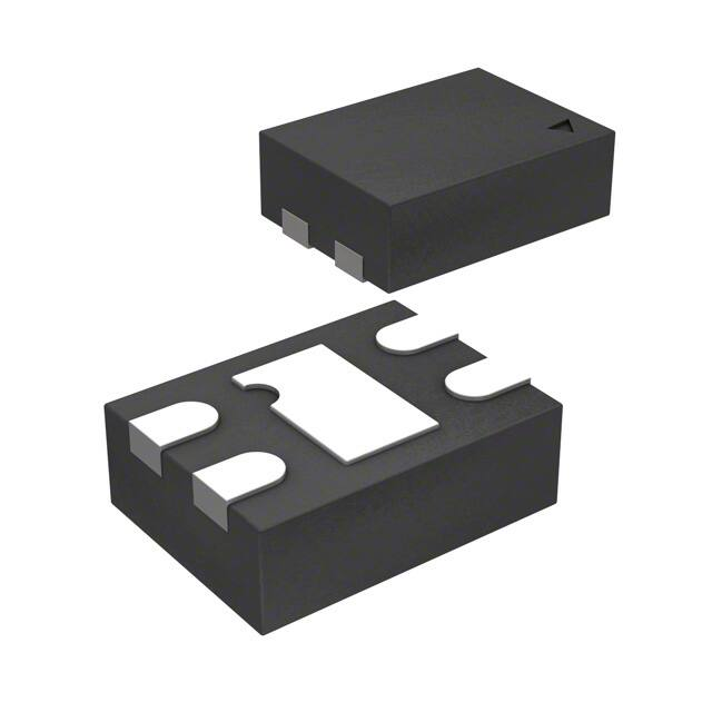
The MIC5303 is available in the ultra small 4-pin 1.2mm x
1.6mm Thin MLF® package, occupying only 1.92mm2 of
PCB area, a 50% reduction in board area compared to
SC-70 and 2mm x 2mm MLF® packages. It’s operating
junction temperature range is –40°C to +125°C and is
available in fixed output voltages in lead-free (RoHS
compliant) Thin MLF® package.
Data sheets and support documentation can be found on
Micrel’s web site at www.micrel.com.
•
•
•
•
•
•
•
•
•
Ultra Small 1.2mm x 1.6mm Thin MLF® package
Low Dropout Voltage: 100mV at 300mA
Output noise 120µVrms
Input voltage range: 2.3V to 5.5V
300mA guaranteed output current
Stable with ceramic output capacitors
Low quiescent current 85µA total
35µs turn-on time
High output accuracy
– ±2% initial accuracy
– ±3% over temperature
• Thermal shutdown and current limit protection
Applications
•
•
•
•
•
•
Mobile Phones
PDAs
GPS Receivers
Portable Media Players
Portable Electronics
Digital Still & Video Cameras
Typical Application
MIC5303-x.xYMT
150
VIN
125
VOUT
100
EN
1µF
Dropout Voltage
vs. Output Current
GND
1µF
75
50
25
RF LDO Application
0
0
VOUT = 2.8V
COUT = 1µF
50 100 150 200 250 300
OUTPUT CURRENT (mA)
ULDO is a trademark of Micrel, Inc.
MLF and MicroLeadFrame are registered trademarks of Amkor Technology, Inc.
Micrel Inc. • 2180 Fortune Drive • San Jose, CA 95131 • USA • tel +1 (408) 944-0800 • fax + 1 (408) 474-1000 • http://www.micrel.com
May 2008
M9999-051508-D
�Micrel, Inc.
MIC5303
Block Diagram
VIN
VOUT
EN
VREF
QuickStart
Thermal
Shutdown
Error
LDO
Amp
Current
Limit
GND
MIC5303 Block Diagram
May 2008
2
M9999-051508-D
�Micrel, Inc.
MIC5303
Ordering Information(1)
Part Number
Marking Code
MIC5303-1.5YMT
1M5
Voltage
Temperature Range
1.5V
Package
–40°C to +125°C
Lead Finish
4-Pin 1.2mm x 1.6mm Thin MLF
®
Pb-Free
®
Pb-Free
MIC5303-1.8YMT
1M8
1.8V
–40°C to +125°C
4-Pin 1.2mm x 1.6mm Thin MLF
MIC5303-2.1YMT
2M1
2.1V
–40°C to +125°C
4-Pin 1.2mm x 1.6mm Thin MLF®
Pb-Free
–40°C to +125°C
4-Pin 1.2mm x 1.6mm Thin MLF
®
Pb-Free
®
Pb-Free
MIC5303-2.5YMT
2M5
2.5V
MIC5303-2.6YMT
2M6
2.6V
–40°C to +125°C
4-Pin 1.2mm x 1.6mm Thin MLF
MIC5303-2.8YMT
2M8
2.8V
–40°C to +125°C
4-Pin 1.2mm x 1.6mm Thin MLF®
Pb-Free
–40°C to +125°C
4-Pin 1.2mm x 1.6mm Thin MLF
®
Pb-Free
®
Pb-Free
MIC5303-2.85YMT
2MN
2.85V
MIC5303-2.9YMT
2M9
2.9V
–40°C to +125°C
4-Pin 1.2mm x 1.6mm Thin MLF
MIC5303-3.0YMT
3M0
3.0V
–40°C to +125°C
4-Pin 1.2mm x 1.6mm Thin MLF®
Pb-Free
–40°C to +125°C
®
Pb-Free
MIC5303-3.3YMT
3M3
3.3V
4-Pin 1.2mm x 1.6mm Thin MLF
Note:
1. Other voltages available. Contact Micrel Marketing for details.
Pin Configuration
EN
1
4
VOUT
GND
2
3
VIN
4-Pin 1.2mm x 1.6mm Thin MLF® (MT)
Pin Description
Pin Number
Pin Name
Pin Function
1
EN
2
GND
Ground
3
VIN
Supply Input
4
VOUT
Output Voltage
HS Pad
EPAD
Exposed heatsink pad connected to ground internally.
May 2008
Enable Input. Active High. High = on, low = off. Do not leave floating.
3
M9999-051508-D
�Micrel, Inc.
MIC5303
Absolute Maximum Ratings(1)
Operating Ratings(2)
Supply Voltage (VIN) ............................................. 0V to +6V
Enable Input (VEN) ................................................ 0V to +6V
Power Dissipation(3)...................................Internally Limited
Lead Temperature (soldering, 5 sec.)........................ 260°C
Junction Temperature (TJ) ........................–40°C to +125°C
Storage Temperature (Ts) .........................–65°C to +150°C
Supply voltage (VIN) ..................................... +2.3V to +5.5V
Enable Input (VEN) .................................................. 0V to VIN
Junction Temperature (TA) ........................ –40°C to +125°C
Junction Thermal Resistance
Thin MLF® -4 (θJA) ...........................................173°C/W
Electrical Characteristics(4)
VIN = VOUT + 1V; COUT = 1.0µF; IOUT = 100µA; TJ = 25°C, bold values indicate –40°C to +125°C, unless noted.
Parameter
Condition
Output Voltage Accuracy
Variation from nominal VOUT
Variation from nominal VOUT; –40°C to +125°C
VIN = VOUT +1V to 5.5V; IOUT = 100µA
Line Regulation
Load Regulation(5)
Dropout Voltage(6)
Ground Pin Current(7)
Ground Pin Current in
Shutdown
Ripple Rejection
Current Limit
Output Voltage Noise
Enable Input
Enable Input Voltage
Enable Input Current
Turn-on Time
Min
Typ
Max
Units
0.02
+2
+3
0.3
0.6
2.0
%
%
%/V
–2
–3
IOUT = 100µA to 150mA
IOUT = 100µA
IOUT = 50mA
IOUT = 150mA
IOUT = 300mA
IOUT = 0 to 300mA, EN = High
VEN = 0V
0.5
0.1
15
50
100
85
0.1
f = up to 1kHz; COUT = 1.0µF
f = 1kHz – 20kHz; COUT = 1.0µF
VOUT = 0V
COUT =1µF, 10Hz to 100kHz
65
42
350
460
120
35
100
200
120
2
850
0.2
Logic Low
Logic High
VIL < 0.2V
VIH > 1.0V
COUT = 1.0µF
1.1
0.01
0.01
35
100
%
mV
mV
mV
mV
µA
µA
dB
dB
mA
µVRMS
V
V
µA
µA
µs
Notes:
1. Exceeding the absolute maximum rating may damage the device.
2. The device is not guaranteed to function outside its operating rating.
3. The maximum allowable power dissipation of any TA (ambient temperature) is PD(max) = (TJ(max) - TA) / θJA. Exceeding the maximum allowable power
dissipation will result in excessive die temperature, and the regulator will go into thermal shutdown.
4. Specification for packaged product only.
5. Regulation is measured at constant junction temperature using low duty cycle pulse testing, changes in output voltage due to heating effects are
covered by the thermal regulation specification.
6. Dropout voltage is defined as the input-to-output differential at which the output voltage drops 2% below its nominal value measured at 1V differential.
7. Ground pin current is the regulator quiescent current. The total current drawn from the supply is the sum of the load current plus the ground pin
current.
May 2008
4
M9999-051508-D
�Micrel, Inc.
MIC5303
Typical Characteristics
Ground Pin Current
vs. Output Current
100
90
90
88
86
84
80
70
60
30
VIN = VOUT + 1V
VOUT = 2.8V
COUT = 1µF
20
10
0
0
90
50 100 150 200 250 300
OUTPUT CURRENT (mA)
Power Supply
Rejection Ratio
160
50mA
80
70
120
150mA
-50 300mA
-40
0
3.0
150
300mA
80
60
-20
40
VIN = VOUT + 1V
-10 VOUT = 2.8V
COUT = 1µF
0
0.1
1
10
100
FREQUENCY (kHz)
150mA
Output Voltage
vs. Output Current
0
3.2
50mA
2.0
2.80
Output Voltage
vs. Supply Voltage
3.00
1.2
2.78
2.77
0
500
VIN = VOUT + 1V
VOUT = 2.8V
COUT = 1µF
100µA
50 100 150 200 250 300
OUTPUT CURRENT (mA)
Current Limit
vs. Input Voltage
300mA
0.4
10
50 100 150 200 250 300
OUTPUT CURRENT (mA)
Output Voltage
vs. Temperature
2.80
2.75
2.70
2.65
2.60
0.8
0
0
VOUT = 2.8V
COUT = 1µF
2.95
2.90
2.85
1.6
2.79
75
0
0
20 40 60 80
TEMPERATURE (°C)
2.4
2.81
Dropout Voltage
vs. Output Current
125
25
100µA
2.8
2.82
5.5
50
20
1,000
3.5
4.0
4.5
5.0
SUPPLY VOLTAGE (V)
100
100
-30
2.83
10
Dropout Voltage
vs. Temperature
-60
100µA
30
20
20 40 60 80
TEMPERATURE (°C)
VOUT = 2.8V
140 COUT = 1µF
300mA
50
40
VIN = VOUT + 1V
VOUT = 2.8V
COUT = 1µF
-70
Ground Pin Current
vs. Supply Voltage
60
100µA
78
76
74
72
70
100
300mA
82
80
50
40
-80
Ground Pin Current
vs. Temperature
COUT = 1µF
1
2
3
4
5
SUPPLY VOLTAGE (V)
6
2.55
2.50
VIN = VOUT + 1V
VOUT = 2.8V
COUT = 1µF
IOUT = 100µA
20 40 60 80
TEMPERATURE (°C)
Output Noise
Spectral Density
490
480
470
1
460
0.1
450
440
430
420
410
400
3.0
May 2008
VOUT = 2.8V
COUT = 1µF
3.5
4.0
4.5
5.0
INPUT VOLTAGE (V)
5.5
0.01 VIN = VOUT + 1V
VOUT = 2.8V
COUT = 1µF
0.001
0.01
0.1
1
10
100 1,000
FREQUENCY (kHz)
5
M9999-051508-D
�Micrel, Inc.
MIC5303
Functional Characteristics
Load Transient Response
Enable
(1V/div)
Output Voltage
(50mV/div)
Enable Turn-On
300mA
VIN = VOUT + 1V
VOUT = 2.8V
Output Current
(100mA/div)
Output Voltage
(1V/div)
COUT = 1µF
VIN = VOUT + 1V
VOUT = 2.8V
COUT = 1µF
Time (10µs/div)
Time (40µs/div)
Line Transient Response
5V
Input Voltage
(2V/div)
4V
VIN = VOUT + 1V
VOUT = 2.8V
COUT = 1µF
Output Voltage
(50mV/div)
IOUT = 10mA
Time (40µs/div)
May 2008
6
M9999-051508-D
�Micrel, Inc.
MIC5303
The actual power dissipation of the regulator circuit can
be determined using the equation:
Application Information
Enable/Shutdown
The MIC5303 comes with an active-high enable pin that
allows the regulator to be disabled. Forcing the enable
pin low disables the regulator and sends it into a “zero”
off-mode-current state. In this state, current consumed
by the regulator goes nearly to zero. Forcing the enable
pin high enables the output voltage. The active-high
enable pin uses CMOS technology and the enable pin
cannot be left floating; a floating enable pin may cause
an indeterminate state on the output.
PD = (VIN – VOUT) IOUT + VIN IGND
Because this device is CMOS and the ground current is
typically
很抱歉,暂时无法提供与“MIC5303-2.9YMT-TR”相匹配的价格&库存,您可以联系我们找货
免费人工找货