MIC5309
Low VIN/VOUT 300mA High PSRR
ULDO™ with Ultra-Low IQ
General Description
Features
The MIC5309 is a high performance, µCap low dropout
regulator, offering ultra-low operating current while
maintaining very fast transient response. The MIC5309
can source up to 300mA of output current and can
regulate down from a low input supply voltage to increase
system efficiency.
Ideal for battery operated applications; the MIC5309 offers
extremely low dropout voltage 100mV typically @ 300mA
load, and low ground current at all load conditions
(typically 23µA). The MIC5309 can also be put into a zerooff-mode current state, drawing virtually no current when
disabled.
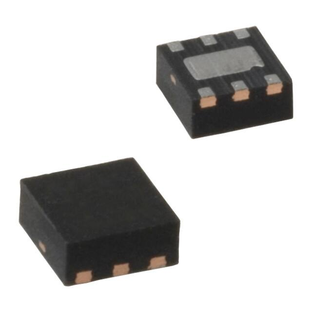
The MIC5309 is available in fixed output voltages in the
tiny 6-pin 1.6mm x 1.6mm thin MLF® leadless package as
well as the 6-pin TSOT-23 for cost sensitive applications.
Data sheets and support documentation can be found on
Micrel’s web site at: www.micrel.com.
•
•
•
•
•
•
•
•
•
•
•
•
•
Input voltage range: 1.7V to 5.5V
Guaranteed 300mA over temperature
Ultra Low dropout voltage of 100mV typical 300mA
High PSRR, up to 90dB @ 1kHz
Output Voltage range: 0.8V to 2.0V
Very low ground current – 23µA under full load
Bias supply voltage range: 2.5V to 5.5V
Stable with 1µF ceramic output capacitor
300mA maximum output current at 1.7V input voltage
Very fast transient response – ideal for digital loads
Thermal shutdown and current limit protection
Tiny 6-pin 1.6mm x 1.6mm Thin MLF® package
Cost effective 6-pin TSOT-23 package
Applications
•
•
•
•
Mobile Phones
PDAs
GPS Receivers
Portable Electronics
___________________________________________________________________________________________________________
Typical Application
MIC5309
BIAS
Li-Ion
2.7V to 4.2V
MIC23050
DC-to-DC
Converter
VIN
CBIAS
1µF
CIN
1µF
VOUT
EN
GND
BYP
CBYP
10nF
COUT
1µF
ULDO is a trademark of Micrel, Inc.
MLF and MicroLeadFrame are registered trademarks of Amkor Technology, Inc.
Micrel Inc. • 2180 Fortune Drive • San Jose, CA 95131 • USA • tel +1 (408) 944-0800 • fax + 1 (408) 474-1000 • http://www.micrel.com
May 2008
M9999-051508-D
�Micrel, Inc.
MIC5309
Ordering Information
Part Number
Voltage
Marking Codes
Temperature Range
Package
MIC5309-1.2YMT
1.2V
▲
MIC5309-1.5YMT
1.5V
▲
1S2
–40° to +125°C
6-Pin 1.6mm x 1.6mm Thin MLF®
1S5
–40° to +125°C
6-Pin 1.6mm x 1.6mm Thin MLF®
MIC5309-1.8YMT
1.8V
▲
1S8
–40° to +125°C
6-Pin 1.6mm x 1.6mm Thin MLF®
MIC5309YMT
Adj.
▲
ASA
–40° to +125°C
6-Pin 1.6mm x 1.6mm Thin MLF®
MIC5309-1.2YD6
MIC5309-1.5YD6
1.2V
QS12
–40° to +125°C
6-Pin TSOT-23
1.5V
QS15
–40° to +125°C
6-Pin TSOT-23
MIC5309-1.8YD6
1.8V
QS18
–40° to +125°C
6-Pin TSOT-23
MIC5309YD6
Adj.
QSAA
–40° to +125°C
6-Pin TSOT-23
Notes
For other voltage options. Contact Micrel Marketing for details.
▲
Pin 1 identifier = .
®
MLF is a GREEN RoHS compliant package. Lead finish is NiPdAu. Mold compound is Halogen Free.
Pin Configuration
BIAS 1
6
BYP/ADJ
GND 2
5
EN
VIN 3
4
VOUT
BIAS
GND
VIN
3
2
1
4
5
6
BYP/ADJ EN
VOUT
6-Pin TSOT-23 (D6)
®
6-Pin 1.6mm x 1.6mm Thin MLF (MT)
Pin Description
Pin Number
Thin MLF-6
Pin Number
Pin Name
Pin Function
3
1
VIN
Power Input for LDO.
2
2
GND
Ground
1
3
BIAS
Bias Input Voltage.
BYP
Bypass: Connect a capacitor to ground to reduce noise and
reduce ripple rejection.
TSOT-23-6
6
4
ADJ
Adjustable: Feedback input from external resistor divider.
5
5
EN
Enable Input: Active High Input. Logic High = On;
Logic Low = Off; Do not leave floating.
4
6
VOUT
Output of regulator.
HS Pad
–
EPAD
Exposed heatsink pad connected to ground internally.
May 2008
2
M9999-051508-D
�Micrel, Inc.
MIC5309
Absolute Maximum Ratings(1)
Operating Ratings(2)
Supply Voltage (VIN) ............................................ 0V to VBIAS
Bias Supply Voltage (VBIAS).................................. 0V to +6V
Enable Voltage (VEN)........................................... 0V to VBIAS
Power Dissipation, ................................ Internally Limited(3)
Lead Temperature (soldering, 10µsec.)..................... 260°C
Storage Temperature (Ts) .........................–65°C to +150°C
ESD Rating(4) .................................................................. 3kV
Supply Voltage (VIN)....................................... +1.7V to VBIAS
Bias Supply Voltage (VBIAS).......................... +2.5V to +5.5V
Enable Input Voltage (VEN)
0V to VBIAS
Junction Temperature (TJ) ........................ –40°C to +125°C
Junction Thermal Resistance
1.6x1.6 MLF-6 (θJA) ...........................................90°C/W
TSOT-23-6 (θJA)...............................................235°C/W
Electrical Characteristics
VBIAS = 3.6V; VIN = VOUT + 1V; VIN ≤ VBIAS; COUT = 1.0µF; IOUT = 100µA; TJ = 25°C, bold values indicate –40°C to +125°C,
unless noted.
Parameter
Condition
Min
Output Voltage Accuracy
Variation from nominal VOUT
–2.0
Reference Voltage
ADJ pin voltage
0.775
0.7905
V
VBIAS Line Regulation
VBIAS = 3.6 to 5.5V, VIN = VOUT + 1V
0.01
0.3
%/V
VIN Line Regulation
VIN = VOUT + 1V , VBIAS = 5.5V
0.02
0.2
%/V
Load Regulation
IOUT = 100µA to 300mA
0.4
2
%
IOUT = 300mA
100
200
mV
IOUT = 100µA to 300mA , VEN = VBIAS
23
35
µA
0.01
2.0
µA
Dropout Voltage
Ground Pin Current
(5)
Ground Pin Current in
Shutdown
VEN ≤ 0.2V
VIN Ripple Rejection
f = up to 1kHz; COUT = 1.0µF; no CBYP
0.7595
f = up to 1kHz; COUT = 1.0µF; CBYP = 10nF
50
f = 20kHz; COUT = 1.0µF; CBYP = 10nF
Current Limit
VOUT = 0V
Output Voltage Noise
COUT = 1.0µF, CBYP = 10nF, 10Hz to 100kHz
350
Typ
Max
Units
+2.0
%
70
dB
90
dB
80
dB
550
800
28
mA
µVRMS
Enable Inputs (EN)
Enable Input Voltage
Logic Low
Turn-on Time
V
1.2
Logic High
Enable Input Current
0.2
V
VIL ≤ 0.2V
0.17
1
µA
VIH ≥ 1.2V
1.5
1
µA
COUT = 1.0µF, CBYP = 10nF
150
500
µs
Notes:
1. Exceeding the absolute maximum rating may damage the device.
2. The device is not guaranteed to function outside its operating rating.
3. The maximum allowable power dissipation of any TA (ambient temperature) is PD(max) = TJ(max) – TA) / θJA. Exceeding the maximum allowable power
dissipation will result in excessive die temperature, and the regulator will go into thermal shutdown.
4. Devices are ESD sensitive. Handling precautions recommended. Human body model, 1.5kΩ in series with 100pF.
5. IGND = IIN + IBIAS – IOUT.
May 2008
3
M9999-051508-D
�Micrel, Inc.
MIC5309
Typical Characteristics
Power Supply
Rejection Ratio (V IN)
-120
100µA
-100
-120
150mA
50mA
-60
100mA
-40
VIN = VOUT + 1V
VOUT = 1.2V
-20 C
OUT = 1µF
CBYP = 0.01µF
0
10
100
1K
10K 100K
FREQUENCY (Hz)
20
18
Ground Current (V IN)
vs. Output Current
VIN = 2.2V
VBIAS = 3.6V
VOUT = 1.2V
COUT = 1µF
16
14
12
12
4
0
0
0
0
Ground Current (V IN)
vs. VIN
40
10
100µA
9
30
300mA
6
5
25
4
3
15
20
VBIAS = 5.5V
VOUT = 1.78V
COUT = 1µF
2
1
May 2008
2.5
50 100 150 200 250 300
OUTPUT CURRENT (mA)
Bias Current
vs. Enable Voltage
3.5
VIN (V)
4.5
5.5
Dropout Voltage
vs. Output Current
100
100µA
300mA
60
1
2
3
4
5
ENABLE VOLTAGE (V)
Output Voltage
vs. Temperature
1.25
1.10
Dropout Voltage
vs. Temperature
COUT = 1µF
300mA
150mA
100µA
6
0
1.30
20 40 60 80
TEMPERATURE (°C)
Output Voltage
vs. Output Current
VIN = 2.2V
VBIAS = 3.6V
VOUT = 1.2V
COUT = 1µF
1.20
VIN = 2.2V
VBIAS = 3.6V
VOUT = 1.2V
COUT = 1µF
IOUT = 100µA
1.15
COUT = 1µF
50 100 150 200 250 300
OUTPUT CURRENT (mA)
20
1.25
1.20
50 100 150 200 250 300
OUTPUT CURRENT (mA)
VIN = 2.2V
VBIAS = 3.6V
COUT = 1µF
CIN = 1µF
CBYP = 0.01µF
40
VBIAS = 5.5V
VOUT = 1.8V
COUT = 1µF
5
1.30
Ground Current (Total)
vs. Output Current
80
10
0
0
12
10
0
120
35
8
7
20 40 60 80
TEMPERATURE (°C)
18
16
14
VIN = 2.2V
VBIAS = 3.6V
COUT = 1µF
CIN = 1µF
CBYP = 0.01µF
2
50 100 150 200 250 300
OUTPUT CURRENT (mA)
100µA
22
20
8
4
2
2
0
28
26
24
14
6
8 300mA
6
4
30
16
6
120
110
100
90
80
70
60
50
40
30
20
10
0
0
Ground Current (V BIAS)
vs. Output Current
10
10
8
0
1.5
300mA
150mA
VIN = 2.8V
VOUT = 1.8V
-20 C
OUT = 1µF
CBYP = 0.01µF
0
10
100
1K
10K 100K 1M
FREQUENCY (Hz)
18
VIN = 2.2V
VBIAS = 3.6V
VOUT = 1.2V
COUT = 1µF
12
10
100µA (no byp)
-40
1M
Ground Current (V IN)
vs. Temperature
18
16
14
-80
-60
300mA
20
100µA
-100
100µA (no byp)
-80
Power Supply
Rejection Ratio (VBIAS)
20 40 60 80
TEMPERATURE (°C)
4
1.15
1.10
0
50 100 150 200 250 300
OUTPUT CURRENT (mA)
M9999-051508-D
�Micrel, Inc.
MIC5309
Typical Characteristics
Output Voltage
vs. V IN
1.5
0.900
100µA
Reference Voltage
vs. Temperature
VIN = 2.2V
VBIAS = 3.6V
VOUT = 1.2V
COUT = 1µF
IOUT = 100µA
0.875
0.850
1.0
0.825
300mA
0.5
150mA
VBIAS = 3.6V
VOUT = 1.2V
COUT = 1µF
0
0 0.5 1 1.5 2 2.5 3 3.5 4 4.5 5 5.5
VIN (V)
10
700
675
650
625
0.800
600
0.775
575
0.750
550
0.725
525
0.700
20 40 60 80
TEMPERATURE (°C)
Current Limit
vs. VIN
VOUT = 1.8V
VBIAS = 3.6V
500
1.5 2 2.5 3 3.5 4 4.5 5 5.5
INPUT VOLTAGE (V)
Output Noise
Spectral Density
1
0.1
0.01 C
OUT = 1µF
CBYP = 0.01µF
ILOAD
0.001
10
100
1K
10K 100K
FREQUENCY (Hz)
May 2008
1M
5
M9999-051508-D
�Micrel, Inc.
MIC5309
Functional Characteristics
May 2008
6
M9999-051508-D
�Micrel, Inc.
MIC5309
Functional Diagram
MIC5309 Block Diagram
May 2008
7
M9999-051508-D
�Micrel, Inc.
MIC5309
Bypass Capacitor
A capacitor can be placed from the noise bypass pin to
ground to reduce output voltage noise. The capacitor
bypasses the internal reference. A 0.01µF capacitor is
recommended for applications that require low-noise
outputs. The bypass capacitor can be increased, further
reducing noise and improving PSRR. Turn-on time
increases slightly with respect to bypass capacitance. A
unique, quick-start circuit allows the MIC5309 to drive a
large capacitor on the bypass pin without significantly
slowing turn-on time.
Applications Information
The MIC5309 is a high performance, low-dropout linear
regulator designed for low current applications requiring
fast transient response. The MIC5309 utilizes two input
supplies, significantly reducing dropout voltage, perfect
for low-voltage, DC-to-DC conversion. The MIC5309
requires a minimum of external components.
The MIC5309 regulator is fully protected from damage
due to fault conditions, offering linear current limiting and
thermal shutdown.
Bias Supply Voltage
VBIAS, requiring relatively light current, provides power to
the control portion of the MIC5309. Bypassing on the
bias pin is recommended to improve performance of the
regulator during line and load transients. 1µF ceramic
capacitor from VBIAS to ground helps reduce high
frequency noise from being injected into the control
circuitry from the bias rail and is good design practice.
Minimum Load Current
The MIC5309, unlike most other regulators, does not
require a minimum load to maintain output voltage
regulation.
Adjustable Regulator Design
The MIC5309 adjustable version allows programming
the output voltage anywhere between 0.8Vand 2V. Two
resistors are used. The resistor values are calculated by:
Input Supply Voltage
VIN provides the supply to power the LDO. The minimum
input voltage is 1.7V, allowing conversion from low
voltage supplies.
⎞
⎛V
R1 = R2 × ⎜⎜ OUT − 1⎟⎟
0
.
775
⎠
⎝
Where VOUT is the desired output voltage.
Output Capacitor
The MIC5309 requires an output capacitor of 1µF or
greater to maintain stability. The design is optimized for
use with low-ESR ceramic chip capacitors. High ESR
capacitors may cause high frequency oscillation. The
output capacitor can be increased, but performance has
been optimized for a 1µF ceramic output capacitor and
does not improve significantly with larger capacitance.
X7R/X5R dielectric-type ceramic capacitors are recommended because of their temperature performance. X7Rtype capacitors change capacitance by 15% over their
operating temperature range and are the most stable
type of ceramic capacitors. Z5U and Y5V dielectric
capacitors change value by as much as 50% and 60%,
respectively, over their operating temperature ranges. To
use a ceramic chip capacitor with Y5V dielectric, the
value must be much higher than an X7R ceramic
capacitor to ensure the same minimum capacitance over
the equivalent operating temperature range.
Enable/Shutdown
The MIC5309 comes with a single active-high enable pin
that allows the regulator to be disabled. Forcing the
enable pin low disables the regulator and sends it into a
“zero” off-mode-current state. In this state, current
consumed by the regulator goes nearly to zero. Forcing
the enable pin high enables the output voltage. The
active-high enable pin uses CMOS technology and the
enable pin cannot be left floating; a floating enable pin
may cause an indeterminate state on the output.
Thermal Considerations
The MIC5309 is designed to provide 300mA of
continuous current in a very small package. Maximum
ambient operating temperature can be calculated based
on the output current and the voltage drop across the
part. Given that the input voltage is 1.8V, the output
voltage is 1.2V and the output current = 300mA. The
actual power dissipation of the regulator circuit can be
determined using the equation:
Input Capacitor
The MIC5309 is a high-performance, high bandwidth
device. Therefore, it requires a well-bypassed input
supply for optimal performance. A 1µF capacitor is
required from the input to ground to provide stability.
Low-ESR ceramic capacitors provide optimal performance at a minimum of space. Additional high-frequency
capacitors, such as small-valued NPO dielectric-type
capacitors, help filter out high-frequency noise and are
good practice in any RF-based circuit.
May 2008
PD = (VIN – VOUT1) I OUT + VIN IGND
Because this device is CMOS and the ground current is
typically