MIC5332
Micro-Power, High-Performance
Dual 300mA ULDO™
General Description
Features
The MIC5332 is a tiny, dual, low quiescent current LDO
ideal for applications that are power sensitive. The
MIC5332 integrates two high-performance 300mA LDOs,
and a power-on-reset (POR) generator into a 2mm x 2mm
Thin MLF® package. This solution occupies the same PC
board area of a single SOT-23 package.
The MIC5332 is designed to reject input noise and provide
low output noise with fast transient response so as to
respond to any load change quickly even though it is a low
quiescent current part. This combination of PSRR, low
noise and transient response, along with low power
consumption makes for a very-high performance, yet
general purpose product.
The MIC5332 is a µCap design, operating with very-small
ceramic output capacitors, which reduces required board
space and component cost. It is available in fixed output
voltages in a tiny 8-pin 2mm x 2mm Thin MLF leadless
package.
Data sheets and support documentation can be found on
Micrel’s web site at: www.micrel.com.
•
•
•
•
•
•
•
•
•
•
2.3V to 5.5V input voltage range
300mA output current per LDO
Very-low quiescent current: 25µA per LDO
POR output with programmable delay on LDO2
High PSRR - >65dB on each LDO
Stable with 1µF ceramic output capacitors
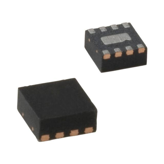
Tiny 8-pin 2mm x 2mm Thin MLF package
Ultra-low dropout voltage – 120mV @ 300mA
Low output voltage noise – 50µVrms
Current-limit and thermal-shutdown protection
Applications
•
•
•
•
•
Camera phones
Mobile phones
PDAs
GPS receivers
Portable devices
___________________________________________________________________________________________________________
Typical Application
Camera DSP Power Supply Circuit
ULDO is a trademark of Micrel, Inc.
MLF and MicroLeadFrame are registered trademarks of Amkor Technology, Inc.
Micrel Inc. • 2180 Fortune Drive • San Jose, CA 95131 • USA • tel +1 (408) 944-0800 • fax + 1 (408) 474-1000 • http://www.micrel.com
September 2012
M9999-091212-B
�Micrel, Inc.
MIC5332
Ordering Information
Marking
Code
Manufacturing
Part Number
Voltage (V)(1, 2)
Junction
Temperature
Range
Package(3)
MIC5332-1.8/1.2YMT
WG4
MIC5332-G4YMT
1.8/1.2
–40° to +125°C
8-Pin 2mm x 2mm Thin MLF
MIC5332-2.5/1.2YMT
WJ4
MIC5332-J4YMT
2.5/1.2
–40° to +125°C
8-Pin 2mm x 2mm Thin MLF
MIC5332-2.8/2.8YMT
WMM
MIC5332-MMYMT
2.8/2.8
–40° to +125°C
8-Pin 2mm x 2mm Thin MLF
MIC5332-2.8/2.85YMT
WMN
MIC5332-MNYMT
2.8/2.85
–40° to +125°C
8-Pin 2mm x 2mm Thin MLF
MIC5332-2.85/2.85YMT
WNN
MIC5332-NNYMT
2.85/2.85
–40° to +125°C
8-Pin 2mm x 2mm Thin MLF
MIC5332-3.0/2.8YMT
WPM
MIC5332-PMYMT
3.0/2.8
–40° to +125°C
8-Pin 2mm x 2mm Thin MLF
MIC5332-3.0/2.85YMT
WPN
MIC5332-PNYMT
3.0/2.85
–40° to +125°C
8-Pin 2mm x 2mm Thin MLF
MIC5332-3.0/3.0YMT
WPP
MIC5332-PPYMT
3.0/3.0
–40° to +125°C
8-Pin 2mm x 2mm Thin MLF
MIC5332-3.3 /3.3YMT
WSS
MIC5332-SSYMT
3.3/3.3
–40° to +125°C
8-Pin 2mm x 2mm Thin MLF
Part Number
Notes:
1.
For other voltage options, contact Micrel Marketing for details.
2.
Pin 1 identifier = .
3.
MLF is a GREEN RoHS-compliant package. Lead finish is NiPdAu. Mold compound is Halogen Free.
▲
Pin Configuration
8-Pin 2mm x 2mm Thin MLF (MT)
(Top View)
Pin Description
Pin Number
Pin Name
Pin Function
1
VIN
Supply Input.
2
GND
Ground.
3
POR2
Power-On Reset Output (Regulator 2): Open-drain output. Active low indicates an output undervoltage condition on regulator 2 when the device is enabled.
4
EN2
Enable Input (Regulator 2): Active High Input. Logic High = On; Logic Low = Off. Do not leave
floating.
5
EN1
Enable Input (Regulator 1): Active High Input. Logic High = On; Logic Low = Off. Do not leave
floating.
6
CSET2
Delay Set Input (Regulator 2): Connect external capacitor to GND to set the internal delay for the
POR2 output. When left open, there is no delay. This pin cannot be grounded.
7
VOUT2
Regulator Output – LDO2.
8
VOUT1
EP
ePad
September 2012
Regulator Output – LDO1.
.Exposed Heat Sink Pad. Connect to GND for best thermal performance.
2
M9999-091212-B
�Micrel, Inc.
MIC5332
Absolute Maximum Ratings(1)
Operating Ratings(2)
Supply Voltage (VIN) ............................................. 0V to +6V
Enable Input Voltage (VEN1, VEN2) .......................... 0V to VIN
POR2 Voltage (VPOR2) .......................................... 0V to +6V
Power Dissipation .................................. Internally Limited(3)
Lead Temperature (soldering, 10sec.)....................... 260°C
Storage Temperature (Ts) .........................–65°C to +150°C
ESD Rating(4) .................................................................. 2kV
Supply Voltage (VIN)..................................... +2.3V to +5.5V
Enable Input Voltage (VEN1, VEN2) .......................... 0V to VIN
POR2 Voltage (VPOR2) ....................................... 0V to +5.5V
Junction Temperature (TJ) ........................ –40°C to +125°C
Junction Thermal Resistance
2mm x 2mm Thin MLF-8 (θJA) ...........................90°C/W
Electrical Characteristics(5)
VIN = VEN1 = VEN2 = VOUT + 1.0V, higher of the two regulator outputs; IOUT1 = IOUT2 = 100µA; COUT1 = COUT2 = 1µF;
TJ = 25°C, bold values indicate –40°C < TJ < +125°C; unless noted.
Parameter
Output Voltage Accuracy
Condition
Min.
Variation from nominal VOUT
–1.0
Typ.
Max.
+1.0
Variation from nominal VOUT; –40°C to +125°C
–2.0
+2.0
Units
%
Line Regulation
VIN = VOUT +1V to 5.5V; IOUT = 100µA
0.02
0.3
0.6
%/V
Load Regulation
IOUT = 100µA to 300mA
0.2
0.5
%
Dropout Voltage
Ground Current
Ground Current in Shutdown
Ripple Rejection
IOUT = 50mA
20
40
mV
IOUT = 300mA
120
240
mV
VEN1 = High; VEN2 = Low; IOUT = 100µA to 300mA
25
50
VEN1 = Low; VEN2 = High; IOUT = 100µA to 300mA
25
50
VEN1 = VEN2 = High; IOUT1= 300mA, IOUT2 = 300mA
40
75
0.01
1.0
VEN1 = VEN2 < 0.2V
f = 1kHz; COUT = 2.2µF;
65
f = 20kHz; COUT = 2.2µF;
45
Current Limit
VOUT = 0V
Output Voltage Noise
COUT=1µF, 10Hz to 100kHz
350
550
µA
µA
dB
800
50
mA
µVRMS
Enable Inputs (EN1/EN2 )
Enable Input Voltage
Enable Input Current
0.2
Logic Low
1.2
Logic High
VIL ≤ 0.2V
0.01
1.0
VIH ≥ 1.2V
0.01
1.0
COUT = 1µF (Enable of First LDO)
140
500
COUT = 1µF (Enable of Second LDO after First Enabled)
110
500
V
µA
Turn-on Time
Turn-On Time (LDO1 and 2)
µs
Notes:
1.
Exceeding the absolute maximum rating may damage the device.
2.
The device is not guaranteed to function outside its operating rating.
3.
The maximum allowable power dissipation of any TA (ambient temperature) is PD(max) = (TJ(max) – TA) / θJA. Exceeding the maximum allowable power
dissipation will result in excessive die temperature, and the regulator will go into thermal shutdown.
4.
Devices are ESD sensitive. Handling precautions recommended. Human body model, 1.5kΩ in series with 100pF.
5.
Specification for packaged product only.
September 2012
3
M9999-091212-B
�Micrel, Inc.
MIC5332
Electrical Characteristics(5) (Continued)
VIN = VEN1 = VEN2 = VOUT + 1.0V, higher of the two regulator outputs; IOUT1 = IOUT2 = 100µA; COUT1 = COUT2 = 1µF;
TJ = 25°C, bold values indicate –40°C < TJ < +125°C; unless noted.
Parameter
Condition
Min.
Typ.
Max.
Units
POR2 Output (LDO2 only)
VTH
Low Threshold, % of VOUT2 (POR2 ON)
88
High Threshold, % of VOUT2 (POR2 OFF)
98
%
0.02
0.1
V
–1.0
0.01
+1.0
µA
VCSET2 = 0V
0.8
1.4
2
µA
POR2 = High
1.21
1.25
1.29
V
VOL
POR2 Output Logic Low Voltage; IL = 250µA
IPOR2
POR2 Leakage Current, POR2 OFF
CSET2 Pin Current Source
CSET2 Pin Threshold Voltage
CSET2 INPUT
September 2012
4
M9999-091212-B
�Micrel, Inc.
MIC5332
Typical Characteristics
PSRR
PSRR
-80
50mA
-80
-70
-60
-50
-40
0.10
-60
-50
300mA
0.08
300mA
-40
0.06
-30
0.04
-20 VIN = 2.3V
-10 VOUT = 1.2V
COUT = 1µF
0
FREQUENCY (Hz)
Dropout Voltage
vs. Temperature
VOUT = 2.8V
0.16 COUT = 1µF
0.14
39
300mA
0.10
0.08
100mA
0.06
0.04
50mA
0.02
10mA
0
-40 -20 0 20 40 60 80 100 120
TEMPERATURE (°C)
Ground Current
vs. Temperature
0
05
Ground Current
vs. Supply Voltage
41
39
Dual LDO Enabled
37
25
2.5
2.820
Single LDO Enabled
3
3.5
4
4.5
5
SUPPLY VOLTAGE (V)
27
5.5
Output Voltage
vs. Load Current
25
05
3.0
2.816
2.9
39
2.812
2.8
2.808
2.7
10mA
100mA
300mA
EN1 = EN2 = VIN
VIN = VOUT + 1V
33
VOUT = 2.8V
COUT = 1µF
30
-40 -20 0 20 40 60 80 100 120
TEMPERATURE (°C)
September 2012
2.804
2.800
05
Ground Current
vs. Load Current
Dual LDO Enabled
35 VIN = VOUT + 1V
VOUT1 = 2.5V
33 VOUT2 = 1.2V
31 COUT1 = 1µF
COUT2 = 1µF
29
42
36
0 100 150 200 250 300
LOAD CURRENT (mA)
37
VOUT1 = 2.5V
35 VOUT2 = 1.2V
COUT1 = 1µF
33
COUT2 = 1µF
31 IOUT1 = 300mA
IOUT2 = 300mA
29
27
VOUT = 2.8V
COUT = 1µF
0.02
FREQUENCY (Hz)
41
0.12
45
0.12
50mA
-70
-30
-20 VIN = 2.3V
V
= 1.2V
-10 OUT
COUT = 2.2µF
0
0.18
0.14
-90
-100
-90
Dropout Voltage
vs. Load Current
VIN = VOUT + 1V
VOUT = 2.8V
COUT = 1µF
0 100 150 200 250 300
LOAD CURRENT (mA)
5
2.6
Single LDO Enabled
0 100 150 200 250 300
LOAD CURRENT (mA)
Output Voltage
vs. Temperature
VIN = VOUT + 1V
VOUT = 2.8V
COUT = 1µF
2.5
-40 -20 0 20 40 60 80 100 120
TEMPERATURE (°C)
M9999-091212-B
�Micrel, Inc.
MIC5332
Typical Characteristics (Continued)
850
800
POR2 Delay vs. CSET2
Current Limit
vs. Supply Voltage
100K
1.0
750
700
650
10K
0.8
VIN = VOUT + 1V
VOUT = 2.8V
COUT = 1µF
Load = 50mA
LDO2
600
550
0.6
0.4
1K
500
450
400
350
2.5
1.2
Output Noise
Spectral Density
CIN = 1µF
COUT = 1µF
3
3.5
4
4.5
5
SUPPLY VOLTAGE (V)
September 2012
5.5
100
100
VIN = 3.6V
VOUT = 1.2V
COUT = 1µF
1K
10K
CSET2 (pF)
6
100K
0.2
0
10
100
1K
10K 100K
FREQUENCY (Hz)
1M
M9999-091212-B
�Micrel, Inc.
MIC5332
Functional Characteristics
September 2012
7
M9999-091212-B
�Micrel, Inc.
MIC5332
Functional Diagram
MIC5332 Block Diagram
September 2012
8
M9999-091212-B
�Micrel, Inc.
MIC5332
Application Information
Enable/Shutdown
The MIC5332 comes with dual active-high enable pins
that allow each regulator to be disabled independently.
Forcing the enable pin low disables the regulator and
sends it into a “zero” off-mode-current state. In this state,
current consumed by the regulator goes nearly to zero.
Forcing the enable pin high enables the output voltage.
The active-high enable pin uses CMOS technology and
the enable pin cannot be left floating; a floating enable
pin may cause an indeterminate state on the output.
MIC5332 is a dual, 300mA LDO, with an integrated
power-on reset (POR) for the second regulator. The
MIC5332 regulator is fully protected from damage due to
fault conditions, offering linear current limiting and
thermal shutdown.
Input Capacitor
The MIC5332 is a high-performance, high-bandwidth
device. Therefore, it requires a well-bypassed input
supply for optimal performance. A 1µF capacitor is
required from the input to ground to provide stability.
Low-ESR
ceramic
capacitors
provide
optimal
performance at a minimum of space. Additional highfrequency capacitors, such as small-valued NPO
dielectric-type capacitors, help filter out high-frequency
noise and are good practice in any RF-based circuit.
X5R or X7R dielectrics are recommended for the input
capacitor. Y5V dielectrics lose most of their capacitance
over temperature and are therefore, not recommended.
Power-On-Reset
The second regulator has a power-on-reset status pin
(POR2). This pin is an open drain output. When LDO2 is
enabled an active low POR2 indicates an undervoltage
condition on VOUT2.
The POR2 status signal can be programmed for a delay
of 1sec/µF by placing a capacitor from the CSET2 pin to
ground. Zero delay is added by leaving the CSET2 pin
open circuit.
Output Capacitor
The MIC5332 requires an output capacitor of 1µF or
greater to maintain stability. The design is optimized for
use with low-ESR ceramic chip capacitors. High-ESR
capacitors may cause high frequency oscillation. The
output capacitor can be increased, but performance has
been optimized for a 1µF ceramic output capacitor and
does not improve significantly with larger capacitance.
X7R/X5R dielectric-type ceramic capacitors are
recommended
because
of
their
temperature
performance. X7R-type capacitors change capacitance
by 15% over their operating temperature range and are
the most stable type of ceramic capacitors. Z5U and
Y5V dielectric capacitors change value by as much as
50% and 60%, respectively, over their operating
temperature ranges. To use a ceramic chip capacitor
with Y5V dielectric, the value must be much higher than
an X7R ceramic capacitor to ensure the same minimum
capacitance over the equivalent operating temperature
range.
Thermal Considerations
The MIC5332 is designed to provide 300mA of
continuous current for both outputs in a very small
package. Maximum ambient operating temperature can
be calculated based upon the output current and the
voltage drop across the part. For example if the input
voltage is 3.6V, the output voltage is 3.0V for VOUT1, 2.8V
for VOUT2 and the output current = 300mA. The actual
power dissipation of the regulator circuit can be
determined using the equation:
PD = (VIN – VOUT1) IOUT1 + (VIN – VOUT2) I OUT2 + VIN IGND
Because this device is CMOS and the ground current is
typically