MIC5333
Micro-Power High Performance
Dual 300mA ULDO™ with Dual POR
General Description
Features
The MIC5333 is a tiny dual low quiescent current LDO
ideal for applications that are power sensitive. The
MIC5333 integrates two high performance, 300mA LDOs,
and a POR generator for each LDO into a 2.5mm x 2.5mm
Thin MLF® package, which occupies less PC board area
than a single SOT-23 package.
The MIC5333 is designed to reject input noise and provide
low output noise with fast transient response to respond to
any load change quickly even though it is a low quiescent
current part. This combination of PSRR, low noise and
transient response along with low power consumption
makes for a very high performance, yet general purpose
product.
The MIC5333 is a µCap design, operating with very small
ceramic output capacitors, which reduces required board
space and component cost; and it is available in fixed
output voltages in the tiny 10-pin 2.5mm x 2.5mm Thin
MLF® leadless package.
Data sheets and support documentation can be found on
Micrel’s web site at: www.micrel.com.
•
•
•
•
•
•
•
•
•
•
•
2.3V to 5.5V input voltage range
300mA output current per LDO
Very low quiescent current: 25µA per LDO
POR output with programmable delay for each LDO
High PSRR – >65dB on each LDO
Stable with 1µF ceramic output capacitors
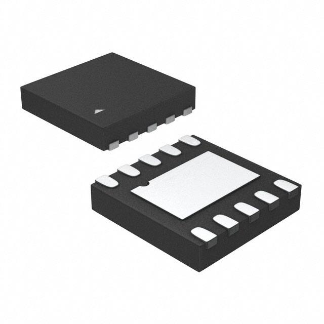
Tiny 10-pin 2.5mm x 2.5mm Thin MLF® package
Ultra-low dropout voltage – 120mV @ 300mA
Low output voltage noise – 50µVrms
Thermal shutdown protection
Current limit protection
Applications
•
•
•
•
•
Camera phones
Mobile phones
PDAs
GPS receivers
Portable devices
___________________________________________________________________________________________________________
Typical Application
MIC5333-xxYMT
VBAT
100k
100k
VIN
VOUT1
I/O
EN1
VOUT2
CORE
EN2
POR1
/RST I/O
CSET1
POR2
/RST CORE
CSET2
1µF
GND
1µF
1µF
Camera DSP
Camera DSP Power Supply Circuit
ULDO is a trademark of Micrel, Inc.
MLF and MicroLeadFrame are registered trademarks of Amkor Technology, Inc.
Micrel Inc. • 2180 Fortune Drive • San Jose, CA 95131 • USA • tel +1 (408) 944-0800 • fax + 1 (408) 474-1000 • http://www.micrel.com
February 2008
M9999-021408-A
�Micrel, Inc.
MIC5333
Ordering Information
Part Number
Manufacturing
Part Number
Marking
Voltage
Junction
Temperature Range
Package
XJ4
2.5V/1.2V
–40° to +125°C
10-Pin 2.5 x 2.5 Thin MLF®
MIC5333-2.5/1.2YMT
MIC5333-J4YMT
MIC5333-2.8/2.8YMT
MIC5333-MMYMT
XMM
2.8V/2.8V
–40° to +125°C
10-Pin 2.5 x 2.5 Thin MLF®
MIC5333-2.8/2.85YMT
MIC5333-MNYMT
XMN
2.8V/2.85V
–40° to +125°C
10-Pin 2.5 x 2.5 Thin MLF®
MIC5333-2.85/2.85YMT
MIC5333-NNYMT
XNN
2.85V/2.85V
–40° to +125°C
10-Pin 2.5 x 2.5 Thin MLF®
MIC5333-3.0/2.8YMT
MIC5333-PMYMT
XPM
3.0V/2.8V
–40° to +125°C
10-Pin 2.5 x 2.5 Thin MLF®
MIC5333-3.0/2.85YMT
MIC5333-PNYMT
XPN
3.0V/2.85V
–40° to +125°C
10-Pin 2.5 x 2.5 Thin MLF®
MIC5333-3.0/3.0YMT
MIC5333-PPYMT
XPP
3.0V/3.0V
–40° to +125°C
10-Pin 2.5 x 2.5 Thin MLF®
Note: Other voltage options available. Contact Micrel for details.
Pin Configuration
VIN
1
10 VOUT1
GND
2
9
VOUT2
POR2
3
8
CSET2
POR1
4
7
CSET1
EN2
5
6
EN1
10-Pin 2.5mm x 2.5mm Thin MLF® (MT)
(Top View)
Pin Description
Pin Number
Pin Name
Pin Function
1
VIN
Supply Input.
2
GND
Ground.
3
POR2
Power-On Reset Output (Regulator 2): Open-drain output. Active low indicates
an output under-voltage condition on regulator 2 when the device is enabled.
4
POR1
Power-On Reset Output (Regulator 1): Open-drain output. Active low indicates
an output under-voltage condition on regulator 1 when the device is enabled.
5
EN2
Enable Input (Regulator 2): Active High Input. Logic High = On; Logic Low =
Off. Do not leave floating.
6
EN1
Enable Input (Regulator 1): Active High Input. Logic High = On; Logic Low =
Off. Do not leave floating.
7
CSET1
Delay Set Input (Regulator 1): Connect external capacitor to GND to set the
internal delay for the POR1 output. When left open, there is no delay. This pin
cannot be grounded.
8
CSET2
Delay Set Input (Regulator 2): Connect external capacitor to GND to set the
internal delay for the POR2 output. When left open, there is no delay. This pin
cannot be grounded.
9
VOUT2
Regulator Output – LDO2.
10
VOUT1
Regulator Output – LDO1.
February 2008
2
M9999-021408-A
�Micrel, Inc.
MIC5333
Absolute Maximum Ratings(1)
Operating Ratings(2)
Supply Voltage (VIN) ............................................. 0V to +6V
Enable Input Voltage (VEN1, VEN2) .......................... 0V to VIN
POR Voltage (VPOR1, VPOR2) ................................. 0V to +6V
Power Dissipation .................................. Internally Limited(3)
Lead Temperature (soldering, 3sec.)......................... 260°C
Storage Temperature (Ts) .........................–65°C to +150°C
ESD Sensitive(4)
Supply Voltage (VIN)..................................... +2.3V to +5.5V
Enable Input Voltage (VEN1, VEN2) .......................... 0V to VIN
POR Voltage (VPOR1, VPOR2) .............................. 0V to +5.5V
Junction Temperature (TJ) ........................ –40°C to +125°C
Junction Thermal Resistance
2.5mm x 2.5mm Thin MLF-10 (θJA) ...................75°C/W
Electrical Characteristics(5)
VIN = VEN1 = VEN2 = VOUT + 1.0V, higher of the two regulator outputs; IOUT1 = IOUT2 = 100µA; COUT1 = COUT2 = 1µF;
TJ = 25°C, bold values indicate –40°C < TJ < +125°C; unless noted.
Parameter
Output Voltage Accuracy
Condition
Min
Typ
Max
Units
Variation from nominal VOUT
–1.0
+1.0
%
Variation from nominal VOUT; –40°C to +125°C
–2.0
+2.0
%
0.3
%/V
Line Regulation
VIN = VOUT +1V to 5.5V; IOUT = 100µA
0.02
0.6
%/V
Load Regulation
IOUT = 100µA to 300mA
0.2
0.5
%
Dropout Voltage
IOUT = 50mA
20
40
mV
IOUT = 300mA
120
240
mV
Ground Current
VEN1 = High; VEN2 = Low; IOUT = 100µA to 300mA
25
50
µA
VEN1 = Low; VEN2 = High; IOUT = 100µA to 300mA
25
50
µA
40
75
µA
0.01
1.0
µA
VEN1 = VEN2 = High; IOUT1= 300mA, IOUT2 = 300mA
Ground Current in Shutdown
VEN1 = VEN2 < 0.2V
Ripple Rejection
f = 1kHz; COUT = 2.2µF
65
f = 20kHz; COUT = 2.2µF
Current Limit
VOUT = 0V
Output Voltage Noise
COUT=1µF; 10Hz to 100kHz
dB
45
350
550
dB
800
50
mA
µVRMS
Enable Inputs (EN1/EN2 )
Enable Input Voltage
Logic Low
0.2
Logic High
Enable Input Current
V
V
1.2
VIL ≤ 0.2V
0.01
1.0
µA
VIH ≥ 1.2V
0.01
1.0
µA
COUT = 1µF (Enable of First LDO)
140
500
µs
COUT = 1µF (Enable of Second LDO after First Enabled)
110
500
µs
Turn-on Time
Turn-on Time (LDO1 and 2)
POR1/POR2 Output
VTH
Low Threshold, % of VOUT (POR ON)
88
%
High Threshold, % of VOUT (POR OFF)
VOL
POR Output Logic Low Voltage; IL = 250µA
IPOR
POR Leakage Current, POR OFF
February 2008
3
–1.0
98
%
0.02
0.1
V
0.01
+1.0
µA
M9999-021408-A
�Micrel, Inc.
Parameter
MIC5333
Condition
Min
Typ
Max
Units
CSET Pin Current Source
VCSET = 0V
0.8
1.4
2
µA
CSET Pin Threshold Voltage
POR = High
1.21
1.25
1.29
V
CSET1/CSET2 INPUT
Notes:
1. Exceeding the absolute maximum rating may damage the device.
2. The device is not guaranteed to function outside its operating rating.
3. The maximum allowable power dissipation of any TA (ambient temperature) is PD(max) = (TJ(max) – TA) / θJA. Exceeding the maximum allowable power
dissipation will result in excessive die temperature, and the regulator will go into thermal shutdown.
4. Devices are ESD sensitive. Handling precautions recommended. Human body model, 1.5kΩ in series with 100pF.
5. Specification for packaged product only.
February 2008
4
M9999-021408-A
�Micrel, Inc.
MIC5333
Typical Characteristics
PSRR
-100
-90
PSRR
-80
50mA
-80
0.10
-60
-50
300mA
0.06
-30
-20 VIN = 2.3V
V
= 1.2V
-10 OUT
COUT = 2.2µF
0
-20 VIN = 2.3V
-10 VOUT = 1.2V
COUT = 1µF
0
Dropout Voltage
vs. Temperature
Ground Current
vs. Supply Voltage
40
38
300mA
0.12
0.08
100mA
0.06
0.04
50mA
0.02
10mA
0
-40 -20 0 20 40 60 80 100 120
TEMPERATURE (°C)
Ground Current
vs. Temperature
39
10mA
100mA
300mA
EN1 = EN2 = VIN
VIN = VOUT + 1V
33
VOUT = 2.8V
COUT = 1µF
30
-40 -20 0 20 40 60 80 100 120
TEMPERATURE (°C)
850
800
20
2
2.820
42
Current Limit
vs. Supply Voltage
0
0
41
Dual LDO Enabled
39
36 VOUT1 = 2.5V
34 VOUT2 = 1.2V
32 COUT1 = 1µF
C
= 1µF
30 OUT2
IOUT1 = 300mA
28 I
OUT2 = 300mA
26
24
22
Single LDO Enabled
27
2.5 3 3.5 4 4.5 5
SUPPLY VOLTAGE (V)
5.5
Output Voltage
vs. Load Current
3.0
2.812
2.8
2.808
2.7
VIN = VOUT + 1V
VOUT = 2.8V
COUT = 1µF
50 100 150 200 250 300
LOAD CURRENT (mA)
100K
2.6
1.0
10K
600
550
Dual LDO Enabled
Single LDO Enabled
50 100 150 200 250 300
LOAD CURRENT (mA)
Output Voltage
vs. Temperature
VIN = VOUT + 1V
VOUT = 2.8V
COUT = 1µF
2.5
-40 -20 0 20 40 60 80 100 120
TEMPERATURE (°C)
1.2
750
0.8
Output Noise
Spectral Density
VIN = VOUT + 1V
VOUT = 2.8V
COUT = 1µF
Load = 50mA
0.6
1K
500
450
400
350
2
25
0
POR Delay vs. CSET
700
650
Ground Current
vs. Load Current
35 VIN = VOUT + 1V
VOUT1 = 2.5V
33 VOUT2 = 1.2V
31 COUT1 = 1µF
COUT2 = 1µF
29
2.9
2.800
0
50 100 150 200 250 300
LOAD CURRENT (mA)
37
2.816
2.804
VOUT = 2.8V
COUT = 1µF
0.02
FREQUENCY (Hz)
0.10
36
0.04
FREQUENCY (Hz)
VOUT = 2.8V
0.16 COUT = 1µF
0.14
45
0.08
300mA
-40
-30
0.18
0.12
50mA
-70
-70
-60
-50
-40
0.14
-90
Dropout Voltage
vs. Load Current
CIN = 1µF
COUT = 1µF
2.5 3 3.5 4 4.5 5
SUPPLY VOLTAGE (V)
February 2008
5.5
100
100
0.4
VIN = 3.6V
VOUT = 1.2V
COUT = 1µF
1K
10K
CSET (pF)
5
100K
0.2
0
10
100
1K
10K 100K
FREQUENCY (Hz)
1M
M9999-021408-A
�Micrel, Inc.
MIC5333
Functional Characteristics
February 2008
6
M9999-021408-A
�Micrel, Inc.
MIC5333
Functional Diagram
MIC5333 Block Diagram
February 2008
7
M9999-021408-A
�Micrel, Inc.
MIC5333
The active-high enable pin uses CMOS technology and
the enable pin cannot be left floating; a floating enable
pin may cause an indeterminate state on the output.
Application Information
MIC5333 is a dual 300mA LDO, with an integrated
Power On Reset (POR) for each of the regulators. The
MIC5333 regulator is fully protected from damage due to
fault conditions, offering linear current limiting and
thermal shutdown.
Power On Reset
Each of the regulator outputs has a Power On Reset
status pin (POR1/POR2). This pin is an open drain
output. When an LDO is enabled an active low POR
indicates an under voltage condition on VOUT.
Each POR status signal can be programmed for a delay
of 1sec/µF by placing a capacitor from its associated
CSET pin to ground. Where the CSET1 pin sets the
delay for the POR1 output and the CSET2 pin sets the
delay for the POR2 output. Zero delay is added by
leaving the CSET1/2 pin open circuit.
Input Capacitor
The MIC5333 is a high-performance, high bandwidth
device. Therefore, it requires a well-bypassed input
supply for optimal performance. A 1µF capacitor is
required from the input to ground to provide stability.
Low-ESR
ceramic
capacitors
provide
optimal
performance at a minimum of space. Additional highfrequency capacitors, such as small-valued NPO
dielectric-type capacitors, help filter out high-frequency
noise and are good practice in any RF-based circuit.
X5R or X7R dielectrics are recommended for the input
capacitor. Y5V dielectrics lose most of their capacitance
over temperature and are therefore, not recommended.
Thermal Considerations
The MIC5333 is designed to provide 300mA of
continuous current for both outputs in a very small
package. Maximum ambient operating temperature can
be calculated based on the output current and the
voltage drop across the part. For example if the input
voltage is 3.6V, the output voltage is 3.0V for VOUT1, 2.8V
for VOUT2 and the output current = 300mA. The actual
power dissipation of the regulator circuit can be
determined using the equation:
PD = (VIN – VOUT1) IOUT1 + (VIN – VOUT2) I OUT2 + VIN IGND
Because this device is CMOS and the ground current is
typically
很抱歉,暂时无法提供与“MIC5333-J4YMT-TR”相匹配的价格&库存,您可以联系我们找货
免费人工找货- 国内价格 香港价格
- 5000+9.986505000+1.29176
- 国内价格 香港价格
- 1+11.892611+1.53831
- 25+9.9972025+1.29314
- 100+9.98653100+1.29176