MIC6211
Operational Amplifier
Features
General Description
•
•
•
•
•
•
•
The MIC6211 op amp is a general-purpose, high
performance, single- or split-supply, operational
amplifier in a space-saving, surface-mount package.
4V to 32V Operation
Small Footprint Package
Unity Gain Stable
2.5 MHz Unity Gain Bandwidth
Rail-to-Rail Output
6 V/μs Typical Slew Rate
Short Circuit Protected
The MIC6211 operates from 4V to 32V, single or
differential (split) supply. The input common-mode
range includes ground. The device features a 2.5 MHz
unity gain bandwidth, 6 V/μs slew rate, and is internally
unity-gain compensated.
Applications
•
•
•
•
•
Inputs are protected against reverse polarity (input
voltage less than V–) and ESD (electrostatic
discharge). Output is current-limited for both sourcing
and sinking. Output short-circuits of unlimited duration
are allowed, provided the power dissipation
specification is not exceeded.
Analog Blocks
Data Acquisition
Sensor Interface
Portable Instrumentation
Active Filtering
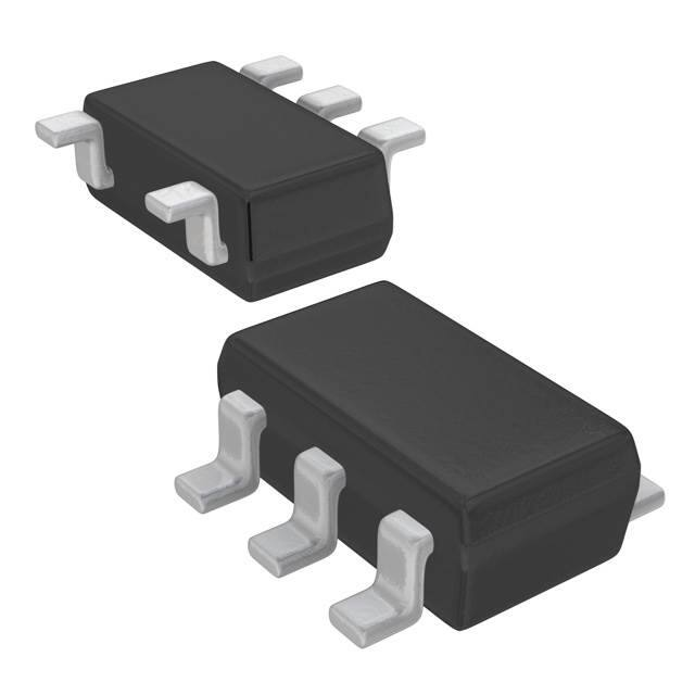
The MIC6211 is available in the tiny, 5-lead SOT-23-5
surface-mount package.
Package Type
Pin Configuration
Functional Configuration
SOT23–5 (M5)
SOT23–5 (M5)
IN+
IN+
V– OUT
3
2
IN–
2020 Microchip Technology Inc.
V– OUT
2
1
Part
Identification
A11
4
3
1
5
4
5
V+
IN–
V+
DS20006346A-page 1
�MIC6211
Functional Diagram
V+
5
20Ω
–IN
1
VOUT
4
20Ω
CC
+IN
3
2
MIC6211
DS20006346A-page 2
V–
(GND)
2020 Microchip Technology Inc.
�MIC6211
1.0
ELECTRICAL CHARACTERISTICS
Absolute Maximum Ratings †
Supply Voltage (VV+ to VV–).......................................................................................................................... 36V or ±18V
Differential Input Voltage (VIN+ to VIN–).....................................................................................................................±36V
Input Voltage (VIN+, VIN–) .................................................................................................................... (VV- – 0.3V) to VV+
Output Short-Circuit Current Duration................................................................................................................ Indefinite
Operating Ratings ‡
Supply Voltage (V+ to V-).............................................................................................................................. +4V to +32V
† Notice: Stresses above those listed under “Absolute Maximum Ratings” may cause permanent damage to the device.
This is a stress rating only and functional operation of the device at those or any other conditions above those indicated
in the operational sections of this specification is not intended. Exposure to maximum rating conditions for extended
periods may affect device reliability.
‡ Notice: The device is not guaranteed to function outside the operating ratings.
2020 Microchip Technology Inc.
DS20006346A-page 3
�MIC6211
ELECTRICAL CHARACTERISTICS (DIFFERENTIAL SUPPLY)
Electrical Characteristics: V+ = +15V, V– = –15V VCM = 0V; RL = 2 kΩ; TA = 25°C, TA= TJ; unless otherwise noted.
Parameters
Symbol
Min.
Typ.
Max.
Units
Input Offset Voltage
VOS
—
2
7
mV
TCVOS
—
7
—
μV/°C
IB
—
50
250
nA
—
Input Offset Current
IOS
—
8
30
nA
—
Input Voltage
Range
VCM
+13.5
+13.8
-15.0
-15.3
—
V
—
Average Input
Offset Drift
Input Bias Current
Conditions
—
(Note 1)
Common-Mode
Rejection Ratio
CMRR
65
100
—
dB
VCM = +13.5V, -15.0V
Power Supply
Rejection Ratio
PSRR
65
110
—
dB
VS = ±2.5V to ±15V
Large-Signal
Voltage Gain
AVOL
25
180
—
V/mV
Maximum Output
Voltage Swing
VOUT
±12.5
±14
—
V
—
Bandwidth
BW
—
2.5
—
MHz
—
Slew Rate
SR
—
6
—
V/μs
—
Short-Circuit Output
Current
ISC
30
50
—
mA
Sourcing or Sinking
Supply Current
IS
—
1.3
2.0
mA
—
Note 1:
VO = ±10V
Not production tested.
DS20006346A-page 4
2020 Microchip Technology Inc.
�MIC6211
ELECTRICAL CHARACTERISTICS (SINGLE SUPPLY)
Electrical Characteristics: V+ = +5V, V- = 0V, VCM = 0.1V; TA = 25°C, TA= TJ; unless otherwise noted.
Parameters
Symbol
Min.
Typ.
Max.
Units
Input Offset Voltage
VOS
—
2
7
mV
TCVOS
—
7
—
μV/°C
IB
—
65
250
nA
—
30
nA
—
—
V
Average Input
Offset Drift
Input Bias Current
Input Offset Current
Input Voltage
Range
IOS
VCM
—
8
+3.5
+3.7
0
-0.3
Conditions
—
(Note 1)
Common-Mode
Rejection Ratio
CMRR
45
70
—
dB
VCM = 0V to 3.5V
Power Supply
Rejection Ratio
PSRR
65
105
—
dB
VS = ±2.5V to ±15V
Large-Signal
Voltage Gain
AVOL
15
170
—
V/mV
Maximum Output
Voltage Swing
VOUT
±3.8
+4.0
—
+1.0
+1.2
V
VO = 1.5V to 3.5V, RL = 2 kΩ
RL = 10 kΩ to GND
RL = 10 kΩ to +5V
Short-Circuit Output
Current
ISC
20
40
—
mA
Sourcing or Sinking
Supply Current
IS
—
1.2
1.8
mA
—
Note 1:
Not production tested.
2020 Microchip Technology Inc.
DS20006346A-page 5
�MIC6211
TEMPERATURE SPECIFICATIONS (Note 1)
Parameters
Symbol
Min.
Typ.
Max.
Units
TA
–40
—
+85
°C
JA
—
200
—
°C/W
Conditions
Temperature Ranges
Ambient Temperature Range
—
Package Thermal Resistance
Thermal Resistance SOT-23-5
Note 1:
Mounted to PCB
The maximum allowable power dissipation is a function of ambient temperature, the maximum allowable
junction temperature and the thermal resistance from junction to air (i.e., TA, TJ, JA). Exceeding the
maximum allowable power dissipation will cause the device operating junction temperature to exceed the
maximum +85°C rating. Sustained junction temperatures above +85°C can impact the device reliability.
DS20006346A-page 6
2020 Microchip Technology Inc.
�MIC6211
The graphs and tables provided following this note are a statistical summary based on a limited number of
samples and are provided for informational purposes only. The performance characteristics listed herein
are not tested or guaranteed. In some graphs or tables, the data presented may be outside the specified
operating range (e.g., outside specified power supply range) and therefore outside the warranted range.
1.5
VS = ±15V
SUPPLY CURRENT (mA)
1.3
1.2
VS = 5V
1.1
1.0
0.5
1.0
-40 -20 0 20 40 60 80 100
TEMPERATURE (oC)
FIGURE 2-1:
Temperature.
Supply Current vs.
0
VOLTAGE GAIN (dB)
VS = 5V
VS = ±15V
60
VS = ±15V
80
60
40
20
0
Input Bias Current vs.
FIGURE 2-5:
Voltage Gain vs. Frequency.
45
30
VS = ±15V
10
VS = 5V
5
VOLTAGE GAIN (dB)
20
15
10,000
FREQUENCY (kHz)
20
PHASE
90
135
10
72 o
0
180
GAIN
PHASE (o)
FIGURE 2-2:
Temperature.
1,000
-20
100
40
0.01
INPUT BIAS CURRENT (nA)
Supply Current vs. Supply
100
30
-40 -20 0 20 40 60 80 100
TEMPERATURE (oC)
INPUT OFFSET CURRENT (nA)
30
120
80
50
5
10 15 20 25
SUPPLY VOLTAGE (V)
FIGURE 2-4:
Voltage.
90
70
0
10
SUPPLY CURRENT (mA)
1.4
1
Note:
TYPICAL PERFORMANCE CURVES
0.1
2.0
225
-10
VS = ±15V
0
-40 -20 0 20 40 60 80 100
TEMPERATURE (oC)
FIGURE 2-3:
Temperature.
Input Offset Current vs.
2020 Microchip Technology Inc.
-20
0.1
FIGURE 2-6:
Frequency.
1.0
FREQUENCY (MHz)
270
10
Gain and Phase vs.
DS20006346A-page 7
�130
30
15
10
110
PSRR (dB)
VS = ±15V
RL = 2k
TA = 25°C
20
100
0
10
80
-PSRR
60
50
0.001 0.01 0.1
1
10
FREQUENCY (kHz)
100
1000 3000
FREQUENCY (kHz)
Large-Signal Frequency
110
VS = ±15V
100
90
80
70
60
50
0.01
+PSRR
90
70
5
FIGURE 2-7:
Response.
CMRR (dB)
VS = ±15V
120
25
0.1
1
10
100 1000
FREQUENCY (kHz)
FIGURE 2-8:
Common Mode Rejection
Ratio vs. Frequency.
DS20006346A-page 8
100
FIGURE 2-9:
Power Supply Rejection
Ratio vs. Frequency.
SHORT CIRCUIT CURRENT (mA)
PEAK-TO-PEAK OUTPUT VOLTAGE (V)
MIC6211
65
60
VS = –15V
55
50
45
40
-40 -20 0 20 40 60 80 100
TEMPERATURE (°C)
FIGURE 2-10:
Temperature.
Short-Circuit Current vs.
2020 Microchip Technology Inc.
�–10V
+10V
OUTPUT VOLTAGE
2μs/DIV
GND
VS = 15V
NOISE VOLTAGE (4μV/DIV)
GND
1s/DIV
–10V
FIGURE 2-11:
Response.
INPUT VOLTAGE
AV = +1
RL = 2k
CL = 10pF
VS = 15V
+10V
Large-Signal Transient
FIGURE 2-13:
0.1 Hz to 10 Hz Noise.
VS = 15V
AV = +1
RL = 2k
CL = 100pF
VS = 15V
+50mV
GND
–50mV
+50mV
NOISE VOLTAGE (5μV/DIV)
INPUT VOLTAGE
OUTPUT VOLTAGE
MIC6211
GND
5ms/DIV
–50mV
500ns/DIV
FIGURE 2-12:
Response.
Small-Signal Transient
2020 Microchip Technology Inc.
FIGURE 2-14:
Wideband Noise.
DS20006346A-page 9
�MIC6211
3.0
PIN DESCRIPTIONS
The descriptions of the pins are listed in Table 3-1.
TABLE 3-1:
PIN FUNCTION TABLE
Pin Number
Symbol
Description
1
OUT
2
V–
Negative Supply. Negative supply for split supply application or ground for single supply
application.
Amplifier Output.
3
IN+
Non-Inverting Input.
4
IN–
Inverting Input.
5
V+
Positive Supply.
DS20006346A-page 10
2020 Microchip Technology Inc.
�MIC6211
4.0
APPLICATION INFORMATION
4.4
4.1
Common-Mode Range and Output
Voltage
Figure 4-3 is a voltage controlled current sink. A buffer
transistor forces current through a programming
resistor until the feedback loop is satisfied. Current flow
is VIN/R. This circuit works with single or split supplies.
The input common-mode range of the MIC6211 is from
the negative supply voltage to 1.2V below the positive
supply voltage. The output voltage swings within 1V of
the positive and negative supply voltage.
4.2
Voltage Buffer
Voltage Controlled Current Sink
3
VIN
1
Figure 4-1 shows a standard voltage follower/buffer.
The output voltage equals the input voltage. This circuit
is used to buffer a high impedance signal source. This
circuit works equally well with single or split supplies.
4
VIN
R
I
3
VIN
1
VOUT
4.5
4
FIGURE 4-1:
Voltage Controlled Current
High-Pass Filter
Figure 4-4 is an active filter with 20 dB (10×) gain and
a low frequency cutoff of 10 Hz. The high
gain-bandwidth of the MIC6211 allows operation
beyond 100 kHz. This filter configuration is designed
for split supplies.
VOUT = VIN
4.3
FIGURE 4-3:
Sink.
R
Voltage Buffer.
Inverting Amplifier
0.1μF
Figure 4-2 shows an inverting amplifier with its gain set
by the ratio of two resistors. This circuit works best with
split supplies, but will perform with single supply
systems if the non-inverting input (+ input) is biased up
above ground.
332k
1μF
1μF
4
VIN
1
7.5k
VOUT
3
R1
VIN
R2
FIGURE 4-4:
4
1
High–Pass Filter.
VOUT
3
VOUT = –VIN
FIGURE 4-2:
⎛
⎜
⎝
R 1⎛
⎜
R2⎝
Inverting Amplifier.
2020 Microchip Technology Inc.
DS20006346A-page 11
�MIC6211
VOUT (dB)
30
20
10
0
100,000
10,000
1,000
100
1
-20
10
-10
1 10
1k
100k
FREQUENCY (Hz)
FIGURE 4-5:
4.6
High-Pass Filter Response.
Summing Amplifier
Figure 4-5 is a single supply summing amplifier. In this
configuration, the output voltage is the sum of V1 and
V2, minus the sum of V3 and V4. By adding more
resistors to either the inverting or non-inverting input,
more voltages may be summed. This single supply
version has one important restriction: the sum of V1
and V2 must exceed the sum of V3 and V4, since the
output voltage cannot pull below zero with only a single
supply.
V1
V2
R
R
3
1
R
VOUT
4
R
R
V3
R
V4
All resistors are equal.
VOUT = V1 + V2 – V3 – V4
V1 + V2 > V3 + V4 for single supply operation
FIGURE 4-6:
DS20006346A-page 12
Summing Amplifier.
2020 Microchip Technology Inc.
�MIC6211
5.0
PACKAGING INFORMATION
5.1
Package Marking Information
5-Lead SOT-23*
(Front)
XXX
5-Lead SOT-23*
(Back)
NNN
Legend: XX...X
Y
YY
WW
NNN
e3
*
Example
A11
Example
469
Product code or customer-specific information
Year code (last digit of calendar year)
Year code (last 2 digits of calendar year)
Week code (week of January 1 is week ‘01’)
Alphanumeric traceability code
Pb-free JEDEC® designator for Matte Tin (Sn)
This package is Pb-free. The Pb-free JEDEC designator ( e3 )
can be found on the outer packaging for this package.
●, ▲, ▼ Pin one index is identified by a dot, delta up, or delta down (triangle
mark).
Note:
In the event the full Microchip part number cannot be marked on one line, it will
be carried over to the next line, thus limiting the number of available
characters for customer-specific information. Package may or may not include
the corporate logo.
Underbar (_) and/or Overbar (‾) symbol may not be to scale.
2020 Microchip Technology Inc.
DS20006346A-page 13
�MIC6211
5-Lead SOT23 Package Outline and Recommended Land Pattern
Note:
For the most current package drawings, please see the Microchip Packaging Specification located at
http://www.microchip.com/packaging.
DS20006346A-page 14
2020 Microchip Technology Inc.
�MIC6211
APPENDIX A:
REVISION HISTORY
Revision A (July 2020)
• Converted Micrel document MIC6211 to Microchip
data sheet template DS20006346A.
• Minor text changes throughout.
2020 Microchip Technology Inc.
DS20006346A-page 15
�MIC6211
NOTES:
DS20006346A-page 16
2020 Microchip Technology Inc.
�MIC6211
PRODUCT IDENTIFICATION SYSTEM
To order or obtain information, e.g., on pricing or delivery, contact your local Microchip representative or sales office.
PART NO.
Device
XX
X
Temperature
-XX
Examples:
a)
MIC6211YM5-TR:
Package Media Type
Device:
MIC6211:
Temperature:
Y
=
–40°C to +85°C
Package:
M5
=
5-Lead SOT-23
Media Type:
TR
=
3,000/Reel
Op Amp, –40°C to +85°C
Junction Temperature
Range, 5-Lead SOT-23
Package, 3,000/Reel
Operational Amplifier
2020 Microchip Technology Inc.
Note 1:
Tape and Reel identifier only appears in the
catalog part number description. This identifier is
used for ordering purposes and is not printed on
the device package. Check with your Microchip
Sales Office for package availability with the
Tape and Reel option.
DS20006346A-page 17
�MIC6211
NOTES:
DS20006346A-page 18
2020 Microchip Technology Inc.
�Note the following details of the code protection feature on Microchip devices:
•
Microchip products meet the specification contained in their particular Microchip Data Sheet.
•
Microchip believes that its family of products is one of the most secure families of its kind on the market today, when used in the
intended manner and under normal conditions.
•
There are dishonest and possibly illegal methods used to breach the code protection feature. All of these methods, to our
knowledge, require using the Microchip products in a manner outside the operating specifications contained in Microchip’s Data
Sheets. Most likely, the person doing so is engaged in theft of intellectual property.
•
Microchip is willing to work with the customer who is concerned about the integrity of their code.
•
Neither Microchip nor any other semiconductor manufacturer can guarantee the security of their code. Code protection does not
mean that we are guaranteeing the product as “unbreakable.”
Code protection is constantly evolving. We at Microchip are committed to continuously improving the code protection features of our
products. Attempts to break Microchip’s code protection feature may be a violation of the Digital Millennium Copyright Act. If such acts
allow unauthorized access to your software or other copyrighted work, you may have a right to sue for relief under that Act.
Information contained in this publication regarding device
applications and the like is provided only for your convenience
and may be superseded by updates. It is your responsibility to
ensure that your application meets with your specifications.
MICROCHIP MAKES NO REPRESENTATIONS OR
WARRANTIES OF ANY KIND WHETHER EXPRESS OR
IMPLIED, WRITTEN OR ORAL, STATUTORY OR
OTHERWISE, RELATED TO THE INFORMATION,
INCLUDING BUT NOT LIMITED TO ITS CONDITION,
QUALITY, PERFORMANCE, MERCHANTABILITY OR
FITNESS FOR PURPOSE. Microchip disclaims all liability
arising from this information and its use. Use of Microchip
devices in life support and/or safety applications is entirely at
the buyer’s risk, and the buyer agrees to defend, indemnify and
hold harmless Microchip from any and all damages, claims,
suits, or expenses resulting from such use. No licenses are
conveyed, implicitly or otherwise, under any Microchip
intellectual property rights unless otherwise stated.
Trademarks
The Microchip name and logo, the Microchip logo, Adaptec,
AnyRate, AVR, AVR logo, AVR Freaks, BesTime, BitCloud, chipKIT,
chipKIT logo, CryptoMemory, CryptoRF, dsPIC, FlashFlex,
flexPWR, HELDO, IGLOO, JukeBlox, KeeLoq, Kleer, LANCheck,
LinkMD, maXStylus, maXTouch, MediaLB, megaAVR, Microsemi,
Microsemi logo, MOST, MOST logo, MPLAB, OptoLyzer,
PackeTime, PIC, picoPower, PICSTART, PIC32 logo, PolarFire,
Prochip Designer, QTouch, SAM-BA, SenGenuity, SpyNIC, SST,
SST Logo, SuperFlash, Symmetricom, SyncServer, Tachyon,
TempTrackr, TimeSource, tinyAVR, UNI/O, Vectron, and XMEGA
are registered trademarks of Microchip Technology Incorporated in
the U.S.A. and other countries.
APT, ClockWorks, The Embedded Control Solutions Company,
EtherSynch, FlashTec, Hyper Speed Control, HyperLight Load,
IntelliMOS, Libero, motorBench, mTouch, Powermite 3, Precision
Edge, ProASIC, ProASIC Plus, ProASIC Plus logo, Quiet-Wire,
SmartFusion, SyncWorld, Temux, TimeCesium, TimeHub,
TimePictra, TimeProvider, Vite, WinPath, and ZL are registered
trademarks of Microchip Technology Incorporated in the U.S.A.
Adjacent Key Suppression, AKS, Analog-for-the-Digital Age, Any
Capacitor, AnyIn, AnyOut, BlueSky, BodyCom, CodeGuard,
CryptoAuthentication, CryptoAutomotive, CryptoCompanion,
CryptoController, dsPICDEM, dsPICDEM.net, Dynamic Average
Matching, DAM, ECAN, EtherGREEN, In-Circuit Serial
Programming, ICSP, INICnet, Inter-Chip Connectivity, JitterBlocker,
KleerNet, KleerNet logo, memBrain, Mindi, MiWi, MPASM, MPF,
MPLAB Certified logo, MPLIB, MPLINK, MultiTRAK, NetDetach,
Omniscient Code Generation, PICDEM, PICDEM.net, PICkit,
PICtail, PowerSmart, PureSilicon, QMatrix, REAL ICE, Ripple
Blocker, SAM-ICE, Serial Quad I/O, SMART-I.S., SQI,
SuperSwitcher, SuperSwitcher II, Total Endurance, TSHARC,
USBCheck, VariSense, ViewSpan, WiperLock, Wireless DNA, and
ZENA are trademarks of Microchip Technology Incorporated in the
U.S.A. and other countries.
SQTP is a service mark of Microchip Technology Incorporated in
the U.S.A.
The Adaptec logo, Frequency on Demand, Silicon Storage
Technology, and Symmcom are registered trademarks of Microchip
Technology Inc. in other countries.
GestIC is a registered trademark of Microchip Technology Germany
II GmbH & Co. KG, a subsidiary of Microchip Technology Inc., in
other countries.
All other trademarks mentioned herein are property of their
respective companies.
© 2020, Microchip Technology Incorporated, All Rights Reserved.
For information regarding Microchip’s Quality Management Systems,
please visit www.microchip.com/quality.
2020 Microchip Technology Inc.
ISBN: 978-1-5224-6417-4
DS20006346A-page 19
�Worldwide Sales and Service
AMERICAS
ASIA/PACIFIC
ASIA/PACIFIC
EUROPE
Corporate Office
2355 West Chandler Blvd.
Chandler, AZ 85224-6199
Tel: 480-792-7200
Fax: 480-792-7277
Technical Support:
http://www.microchip.com/
support
Web Address:
www.microchip.com
Australia - Sydney
Tel: 61-2-9868-6733
India - Bangalore
Tel: 91-80-3090-4444
China - Beijing
Tel: 86-10-8569-7000
India - New Delhi
Tel: 91-11-4160-8631
Austria - Wels
Tel: 43-7242-2244-39
Fax: 43-7242-2244-393
China - Chengdu
Tel: 86-28-8665-5511
India - Pune
Tel: 91-20-4121-0141
Denmark - Copenhagen
Tel: 45-4485-5910
Fax: 45-4485-2829
China - Chongqing
Tel: 86-23-8980-9588
Japan - Osaka
Tel: 81-6-6152-7160
Finland - Espoo
Tel: 358-9-4520-820
China - Dongguan
Tel: 86-769-8702-9880
Japan - Tokyo
Tel: 81-3-6880- 3770
China - Guangzhou
Tel: 86-20-8755-8029
Korea - Daegu
Tel: 82-53-744-4301
France - Paris
Tel: 33-1-69-53-63-20
Fax: 33-1-69-30-90-79
China - Hangzhou
Tel: 86-571-8792-8115
Korea - Seoul
Tel: 82-2-554-7200
China - Hong Kong SAR
Tel: 852-2943-5100
Malaysia - Kuala Lumpur
Tel: 60-3-7651-7906
China - Nanjing
Tel: 86-25-8473-2460
Malaysia - Penang
Tel: 60-4-227-8870
China - Qingdao
Tel: 86-532-8502-7355
Philippines - Manila
Tel: 63-2-634-9065
China - Shanghai
Tel: 86-21-3326-8000
Singapore
Tel: 65-6334-8870
Germany - Munich
Tel: 49-89-627-144-0
Fax: 49-89-627-144-44
China - Shenyang
Tel: 86-24-2334-2829
Taiwan - Hsin Chu
Tel: 886-3-577-8366
Germany - Rosenheim
Tel: 49-8031-354-560
China - Shenzhen
Tel: 86-755-8864-2200
Taiwan - Kaohsiung
Tel: 886-7-213-7830
Israel - Ra’anana
Tel: 972-9-744-7705
China - Suzhou
Tel: 86-186-6233-1526
Taiwan - Taipei
Tel: 886-2-2508-8600
China - Wuhan
Tel: 86-27-5980-5300
Thailand - Bangkok
Tel: 66-2-694-1351
Italy - Milan
Tel: 39-0331-742611
Fax: 39-0331-466781
China - Xian
Tel: 86-29-8833-7252
Vietnam - Ho Chi Minh
Tel: 84-28-5448-2100
Atlanta
Duluth, GA
Tel: 678-957-9614
Fax: 678-957-1455
Austin, TX
Tel: 512-257-3370
Boston
Westborough, MA
Tel: 774-760-0087
Fax: 774-760-0088
Chicago
Itasca, IL
Tel: 630-285-0071
Fax: 630-285-0075
Dallas
Addison, TX
Tel: 972-818-7423
Fax: 972-818-2924
Detroit
Novi, MI
Tel: 248-848-4000
Houston, TX
Tel: 281-894-5983
Indianapolis
Noblesville, IN
Tel: 317-773-8323
Fax: 317-773-5453
Tel: 317-536-2380
Los Angeles
Mission Viejo, CA
Tel: 949-462-9523
Fax: 949-462-9608
Tel: 951-273-7800
Raleigh, NC
Tel: 919-844-7510
New York, NY
Tel: 631-435-6000
San Jose, CA
Tel: 408-735-9110
Tel: 408-436-4270
Canada - Toronto
Tel: 905-695-1980
Fax: 905-695-2078
DS20006346A-page 20
China - Xiamen
Tel: 86-592-2388138
China - Zhuhai
Tel: 86-756-3210040
Germany - Garching
Tel: 49-8931-9700
Germany - Haan
Tel: 49-2129-3766400
Germany - Heilbronn
Tel: 49-7131-72400
Germany - Karlsruhe
Tel: 49-721-625370
Italy - Padova
Tel: 39-049-7625286
Netherlands - Drunen
Tel: 31-416-690399
Fax: 31-416-690340
Norway - Trondheim
Tel: 47-7288-4388
Poland - Warsaw
Tel: 48-22-3325737
Romania - Bucharest
Tel: 40-21-407-87-50
Spain - Madrid
Tel: 34-91-708-08-90
Fax: 34-91-708-08-91
Sweden - Gothenberg
Tel: 46-31-704-60-40
Sweden - Stockholm
Tel: 46-8-5090-4654
UK - Wokingham
Tel: 44-118-921-5800
Fax: 44-118-921-5820
2020 Microchip Technology Inc.
02/28/20
�