MIC914
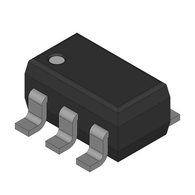
160MHz Low-Power SOT23-5 Op Amp
General Description
Features
The MIC914 is a high-speed, operational amplifier with a
gain-bandwidth product of 160MHz. The part is unity gain
stable provided its output is loaded with at least 200Ω. It
has a very low 1.25mA supply current, and features the
IttlyBitty® SOT-23-5 package.
Supply voltage range is from ±2.5V to ±9V, allowing the
MIC914 to be used in low-voltage circuits or applications
requiring large dynamic range.
The MIC914 is stable driving any capacitive load and
achieves excellent PSRR, making it much easier to use
than most conventional high-speed devices. Low supply
voltage, low power consumption, and small packing make
the MIC914 ideal for portable equipment. The ability to
drive capacitive loads also makes it possible to drive long
coaxial cables.
Data sheets and support documentation can be found on
Micrel’s web site at: www.micrel.com.
•
•
•
•
•
•
•
•
160MHz gain bandwidth product
1.25mA supply current
SOT23-5 package
160V/µs slew rate
Drives any capacitive load
112dB CMRR
Unconditionally stable with gain of +2 or –1
Conditionally stable with gain of +1
Applications
•
•
•
•
•
•
Video
Imaging
Ultrasound
Portable equipment
Line drivers
XDSL
___________________________________________________________________________________________________________
Ordering Information
Part Number
Temperature Range
Package
Lead Finish
MIC914BM5
–40° to +85°C
5-Pin SOT23
Standard
MIC914YM5
–40° to +85°C
5-Pin SOT23
Pb-Free
Micrel Inc. • 2180 Fortune Drive • San Jose, CA 95131 • USA • tel +1 (408) 944-0800 • fax + 1 (408) 474-1000 • http://www.micrel.com
October 2007
M9999-101807
�Micrel, Inc.
MIC914
Pin Configuration
Functional Pinout
IN+
3
V+ OUT
2
1
IN+
3
Part
Identification
V+ OUT
2
1
A24
4
5
4
5
IN–
V–
IN–
V–
SOT23-5
SOT23-5
Pin Description
Pin Number
Pin Name
1
OUT
2
V+
Positive Supply (Input)
3
IN+
Non-inverting Input
4
IN–
Inverting Input
5
V–
Negative Supply (Input)
October 2007
Pin Function
Output: Amplifier Output
2
M9999-101807
�Micrel, Inc.
MIC914
Absolute Maximum Ratings(1)
Operating Ratings(2)
Supply Voltage (VV+ – VV–) .............................................20V
Differential Input Voltage (|VIN+ – VIN–|)(3) .........................4V
Input Common-Mode Range (VIN+ – VIN–) .............VV+ to VV–
Lead Temperature (soldering, 5 sec.)........................ 260°C
Storage Temperature (Ts) .......................................... 150°C
ESD Rating(4) ............................................................... 1.5kV
Supply Voltage (VS)......................................... ±2.5V to ±9V
Junction Temperature (TJ) .......................... –40°C to +85°C
Thermal Resistance ...............................................260°C/W
Electrical Characteristics (±5V)
VV+ = +5V, VV– = –5V, VCM = 0V, VOUT = 0V; RL = 10MΩ; TJ = 25°C, bold values indicate –40°C ≤ TJ ≤ +85°C; unless noted.
Symbol
VOS
IB
IOS
Parameter
Condition
Min
Typ
Max
Input Offset Voltage
1
16
Input Offset Voltage
Temperature Coefficient
4
Input Bias Current
5.5
Input Offset Current
0.05
–3.25
Units
mV
µV/°C
9
µA
15
µA
3
µA
VCM
Input Common-Mode Range
CMRR > 60dB
CMRR
Common-Mode Rejection Ratio
–2.0V < VCM < +2.0V
70
85
+3.25
dB
PSRR
Power Supply Rejection Ratio
±5V < VS < ±9V
70
81
dB
AVOL
Large-Signal Voltage Gain
RL = 2k, VOUT = ±2V
60
71
dB
RL = 200Ω, VOUT = ±2V
60
71
dB
+3.3
3.5
dB
65
VOUT
Maximum Output Voltage Swing
positive, RL = 2kΩ
V
V
+3.0
negative, RL = 2kΩ
–3.5
positive, RL = 200Ω
+3.0
–3.3
V
–3.0
V
3.2
V
V
+2.75
negative, RL = 200Ω
V
–2.8
–2.45
V
–2.2
V
GBW
Gain-Bandwidth Product
f = 80MHz, RL = 1kΩ
BW
–3dB Bandwidth
AV = 2, RL = 150Ω
213
MHz
AV = 4, or AV = –3, RL = 400Ω
104
MHz
RF = RG = 470Ω, AV = 2, VOUT = 2Vpp,
f = 2MHz
0.01
%
AV = 2, VOUT = 2Vpp, f = 2MHz, RL = 500Ω
0.05
%
350
V/µs
72
mA
THD
Total Harmonic Distortion
SR
Slew Rate
IGND
Short-Circuit Output Current
source
sink
MHz
25
Supply Current
October 2007
300
4.1
3
mA
4.9
mA
5.4
mA
M9999-101807
�Micrel, Inc.
MIC914
Electrical Characteristics
VV+ = +9V, VV– = –9V, VCM = 0V, VOUT = 0V; RL = 10MΩ; TJ = 25°C, bold values indicate –40°C ≤ TJ ≤ +85°C; unless noted.
Symbol
Parameter
VOS
Condition
Min
Typ
Max
Units
Input Offset Voltage
1
16
mV
Input Offset Voltage
Temperature Coefficient
4
µV/°C
IB
Input Bias Current
5.5
IOS
Input Offset Current
0.05
VCM
Input Common-Mode Range
CMRR
Common-Mode Rejection Ratio
–6.0V < VCM < 6.0V
70
88
dB
AVOL
Large-Signal Voltage Gain
RL = 2kΩ, VOUT = ±6V
60
73
dB
VOUT
Maximum Output Voltage Swing
positive, RL = 2kΩ
+7.2
+7.4
V
CMRR > 60dB
–7.25
9
15
µA
3
µA
+7.25
V
V
+6.8
negative, RL = 2kΩ
µA
–7.4
–7.2
V
–6.8
V
GBW
Gain-Bandwidth Product
RL = 1kΩ, f = 80MHz
350
MHz
BW
–3dB Bandwidth
AV = 2 or AV = –1, RL = 150Ω
240
MHz
AV = 4 or AV = –3
140
MHz
RF = RG = 470Ω, AV = 2, VOUT = 2Vpp,
f = 2MHz
0.01
%
AV = 2, VOUT = 2Vpp, f = 2MHz, RL = 500Ω
0.04
%
500
V/µs
source
90
mA
sink
32
mA
THD
Total Harmonic Distortion
SR
Slew Rate
IGND
Short-Circuit Output Current
Supply Current
4.2
5.0
mA
5.5
mA
Notes:
1. Exceeding the absolute maximum rating may damage the device.
2. The device is not guaranteed to function outside its operating rating.
3. Exceeding the maximum differential input voltage will damage the input stage and degrade performance (in particular, input bias current is likely to
change).
4. Devices are ESD sensitive. Handling precautions recommended. Human body model, 1.5k in series with 100pF.
October 2007
4
M9999-101807
�Micrel, Inc.
MIC914
Test Circuits
VCC
10µF
VCC
0.1µF
Input
R2
BNC
5k
10µF
0.1µF
10k
10k
10k
2k
4
MIC913
BNC
1
BNC
Input
2
R1 5k
Output
4
R7c 2k
2
0.1µF
MIC913
3
1
BNC
Output
3
5
5
0.1µF
R6
Input
0.1F
BNC
5k
R3
200k
0.1µF
All resistors:
1% metal film
All resistors 1%
R5
5k
10µF
VEE
R4
10µF
⎛ R2 R2 + R 5 + R4 ⎞
VOUT = VERROR ⎜ 1+
+
⎟
⎝ R1
⎠
R7
PSRR vs. Frequency
CMRR vs. Frequency
VEE
100pF
10pF
R1
R3 27k
S1
S2
R5
R4 27k
VCC
R2 4k
4
10µF
2
0.1µF
MIC913
1
3
5
10pF
0.1µF
BNC
To
Dynamic
Analyzer
10µF
VEE
Noise Measurement
October 2007
5
M9999-101807
�Micrel, Inc.
MIC914
Typical Characteristics
October 2007
6
M9999-101807
�Micrel, Inc.
MIC914
Typical Characteristics (continued)
October 2007
7
M9999-101807
�Micrel, Inc.
MIC914
Typical Characteristics (continued)
October 2007
8
M9999-101807
�Micrel, Inc.
MIC914
Typical Characteristics (continued)
October 2007
9
M9999-101807
�Micrel, Inc.
MIC914
Functional Characteristics
October 2007
10
M9999-101807
�Micrel, Inc.
MIC914
Functional Characteristics (continued)
October 2007
11
M9999-101807
�Micrel, Inc.
MIC914
It is important to ensure adequate supply bypassing
capacitors are located close to the device.
Application Information
The MIC913 is a high-speed, voltage-feedback operational amplifier featuring very low supply current. The
MIC913 is not unity-gain stable, it requires a minimum
gain of +2 or –1 to ensure stability. The device is
however stable even when driving high capacitance
loads.
Power Supply Bypassing
Regular supply bypassing techniques are recommended. A 10µF capacitor in parallel with a 0.1µF
capacitor on both the positive and negative supplies are
ideal. For best performance all bypassing capacitors
should be located as close to the op amp as possible
and all capacitors should be low ESL (equivalent series
inductance), ESR (equivalent series resistance).
Surface-mount ceramic capacitors are ideal.
Driving High Capacitance
The MIC913 is stable when driving any capacitance (see
“Typical Characteristics: Gain Bandwidth and Phase
Margin vs. Load Capacitance”) making it ideal for driving
long coaxial cables or other high-capacitance loads.
Phase margin remains constant as load capacitance is
increased. Most high-speed op amps are only able to
drive limited capacitance.
Note: increasing load capacitance does reduce
the speed of the device (see “Typical Characteristics: Gain Bandwidth and Phase Margin vs.
Load”). In applications where the load capacitance reduces the speed of the op amp to an
unacceptable level, the effect of the load capacitance can be reduced by adding a small resistor
(