MIC920
Micrel, Inc.
MIC920
80MHz Low-Power SC-70 Op Amp
General Description
Features
The MIC920 is a high-speed operational amplifier with a
gain-bandwidth product of 80MHz. The part is unity gain
stable. It has a very low 550µA supply current, and features
the SC-70 package.
Supply voltage range is from ±2.5V to ±9V, allowing the
MIC920 to be used in low-voltage circuits or applications
requiring large dynamic range.
The MIC920 is stable driving any capacitative load and
achieves excellent PSRR and CMRR, making it much easier
to use than most conventional high-speed devices. Low
supply voltage, low power consumption, and small packing
make the MIC920 ideal for portable equipment. The ability
to drive capacitative loads also makes it possible to drive
long coaxial cables.
•
•
•
•
•
•
•
80MHz gain bandwidth product
115MHz –3dB bandwidth
550µA supply current
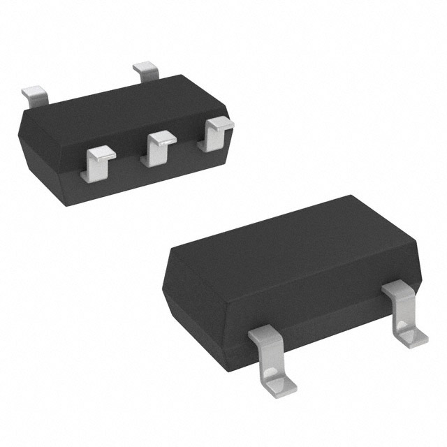
SC-70 or SOT-23-5 packages
3000V/µs slew rate
Drives any capacitive load
Unity gain stable
Applications
•
•
•
•
•
Video
Imaging
Ultrasound
Portable equipment
Line drivers
Ordering Information
Part Number
Standard
Marking
MIC920BM5
A37
MIC920BC5
A37
Pb-Free
MIC920YC5
Marking
Ambient Temperature
Package
–40ºC to +85ºC
SOT-23-5*
–40ºC to +85ºC
SC-70-5
A37
* Contact factory for availability of SOT-23-5 package.
Note: Underbar marking may not be to scale.
Functional Pinout
Pin Configuration
IN– V– IN+
3
2
1
A37
IN–
Part
Identification
3
V– IN+
2
1
4
5
4
5
OUT
V+
OUT
V+
SOT-23-5 or SC-70
SOT-23-5 or SC-70
Pin Description
Pin Number
Pin Name
1
IN+
Pin Function
Noninverting Input
2
V–
Negative Supply (Input)
3
IN–
Inverting Input
4
OUT
Output: Amplifier Output
5
V+
Positive Supply (Input)
Micrel, Inc. • 2180 Fortune Drive • San Jose, CA 95131 • USA • tel + 1 (408) 944-0800 • fax + 1 (408) 474-1000 • http://www.micrel.com
March 2006
1
MIC920
�MIC920
Micrel, Inc.
Absolute Maximum Ratings (Note 1)
Operating Ratings (Note 2)
Supply Voltage (VV+ – VV–) ........................................... 20V
Differentail Input Voltage (VIN+ – VIN–) ........... 4V, Note 3
Input Common-Mode Range (VIN+, VIN–) ............VV+ to VV–
Lead Temperature (soldering, 5 sec.) ........................ 260°C
Storage Temperature (TS) ......................................... 150°C
ESD Rating, Note 4 ................................................... 1.5kV
Supply Voltage (VS) .........................................±2.5V to ±9V
Junction Temperature (TJ) .......................... –40°C to +85°C
Package Thermal Resistance..............................................
SOT-23-5 ........................................................... 260°C/W
SC-70-5 ............................................................. 450°C/W
Electrical Characteristics (±5V)
V+ = +5V, V– = –5V, VCM = 0V, RL = 10MΩ; TJ = 25°C, bold values indicate –40°C ≤ TJ ≤ +85°C; unless noted.
Symbol
Parameter
VOS
Input Offset Voltage
IB
Input Bias Current
VOS
VOS Temperature Coefficient
IOS
Input Offset Current
VCM
Input Common-Mode Range
CMRR
Common-Mode Rejection Ratio
PSRR
Power Supply Rejection Ratio
AVOL
Large-Signal Voltage Gain
VOUT
Maximum Output Voltage Swing
Condition
Min
Unity Gain-Bandwidth Product
PM
Phase Margin
Max
Units
5
mV
1
0.26
0.04
CMRR > 72dB
–3.25
µV/°C
0.6
µA
0.3
µA
+3.25
V
–2.5V < VCM < +2.5V
75
85
dB
95
104
dB
RL = 2k, VOUT = ±2V
65
82
dB
85
dB
±3.5V < VS < ±9V
RL = 100Ω, VOUT = ±1V
positive, RL = 2kΩ
+3.0
positive, RL = 200Ω
+1.5
negative, RL = 2kΩ
GBW
Typ
0.43
3.6
–3.6
negative, RL = 200Ω, Note 5
Av = 1, RL = 1kΩ, CL = 1.7pF
V
–1.0
V
3.0
–2.5
CL = 1.7pF
V
–3.0
V
67
MHz
32
°
100
MHz
1350
V/µs
63
mA
BW
–3dB Bandwidth
SR
Slew Rate
C=1.7pF, Gain=1, VOUT=5V, peak to peak,
positive SR = 1190V/µs
ISC
Short-Circuit Output Current
source
45
sink
20
IS
Supply Current
No Load
0.55
Input Voltage Noise
f = 10kHz
11
V/√Hz
Input Current Noise
f = 10kHz
0.7
A/√Hz
45
mA
0.80
mA
Electrical Characteristics
V+ = +9V, V– = –9V, VCM = 0V, RL = 10MΩ; TJ = 25°C, bold values indicate –40°C ≤ TJ ≤ +85°C; unless noted
Symbol
Parameter
VOS
Input Offset Voltage
VOS
Condition
Min
Input Offset Voltage
Temperature Coefficient
Typ
Max
0.3
5
1
Units
mV
µV/°C
Input Bias Current
0.23
0.60
µA
IOS
Input Offset Current
0.04
0.3
µA
Input Common-Mode Range
CMRR > 75dB
CMRR
Common-Mode Rejection Ratio
PSRR
Power Supply Rejection Ratio
–6.5V < VCM < +6.5V
IB
VCM
MIC920
±3.5V < VS < ±9V
2
–7.25
+7.25
V
60
91
dB
95
104
dB
March 2006
�MIC920
Micrel, Inc.
Symbol
Parameter
Condition
Min
Typ
AVOL
Large-Signal Voltage Gain
RL = 2k, VOUT = ±2V
75
84
dB
93
dB
VOUT
Maximum Output Voltage Swing
positive, RL = 2kΩ
6.5
GBW
Unity Gain-Bandwidth Product
PM
Phase Margin
RL = 100Ω, VOUT = ±1V
negative, RL = 2kΩ
7.5
–7.5
CL = 1.7pF
AV = 1, RL = 1kΩ, CL = 1.7pF
Max
Units
V
–6.2
V
80
MHz
30
°
115
MHz
3000
V/µs
65
mA
BW
–3dB Bandwidth
SR
Slew Rate
C=1.7pF, Gain=1, VOUT=5V, peak to peak,
negative SR = 2500V/µs
ISC
Short-Circuit Output Current
source
50
sink
30
IS
Supply Current
No Load
0.55
Input Voltage Noise
f = 10kHz
10
V/√Hz
Input Current Noise
f = 10kHz
0.8
A/√Hz
50
mA
0.8
mA
Note 1.
Exceeding the absolute maximum rating may damage the device.
Note 2.
The device is not guaranteed to function outside its operating rating.
Note 3.
Exceeding the maximum differential input voltage will damage the input stage and degrade performance (in particular, input bias current is
likely to change).
Note 4.
Devices are ESD sensitive. Handling precautions recommended. Human body model, 1.5k in series with 100pF.
Note 5.
Output swing limited by the maximum output sink capability, refer to the short-circuit current vs. temperature graph in “Typical Characteristics.”
March 2006
3
MIC920
�MIC920
Micrel, Inc.
Test Circuits
V+
10µF
V+
Input
0.1µF
50Ω
BNC
R2
5k
10µF
0.1µF
10k
10k
10k
2k
3
1
5
MIC920
4
BNC
Input
R1 5k
BNC
R7c 2k
Output
1
R7b 200Ω
R7a 100Ω
2
50Ω
Input
3
5k
R3
200k
50
All resistors:
1% metal film
0.1µF
All resistors 1%
MIC920
2
4
BNC
Output
0.1µF
R5
5k
10µF
V–
R4
250Ω
R2 R2 + R 5 + R4
VOUT = VERROR 1 +
+
R1
R7
10µF
V–
PSRR vs. Frequency
100pF
0.1µF
R6
0.1µF
BNC
5
CMRR vs. Frequency
V+
V+
10µF
10pF
R1
20Ω
R3 27k
S1
S2
R5
20Ω
R2 4k
3
3
1
R4 27k
10µF
5
0.1µF
MIC920
2
10pF
4
0.1F
BNC
To
Dynamic
Analyzer
VIN
0.1µµF
MIC920
2
300Ω
4
0.1µF
50Ω
1k
VOUT
FET Probe
CL
10µF
10µF
V–
V–
Closed Loop Frequency Response Measurement
Noise Measurement
MIC920
1
5
4
March 2006
�MIC920
Micrel, Inc.
Typical Characteristics
0.50
0.45
V± = ±9V
1
0.40
0.35
0.95
0.9
-40 -20 0 20 40 60 80 100
TEMPERATURE °C)
(
0.30
-40 -20 0 20 40 60 80 100
TEMPERATURE °C)
(
Offset Voltage vs.
Common-Mode Voltage
SHORT-CIRCUIT CURRENT (mA)
84
80
76
72
68
64
60
56
52
48
44
40
2.0
–40°C
25°C
85°C
3.4 4.8 6.2 7.6 9.0
SUPPLY VOLTAGE (V)
Output Voltage vs.
Output Current (Sinking)
V± = ±5V
–40°C
45.0
40.5
36.0
31.5
27.0
22.5
18.0
13.5
9.0
4.5
0
OUTPUT VOLTAGE (V)
0.5
85°C
0
-0.5
-1.0
-1.5
-2.0 25°C
-2.5
-3.0
-3.5
-4.0
-4.5
-5.0
OUTPUT CURRENT (mA)
March 2006
Offset Voltage vs.
Common-Mode Voltage
OFFSET VOLTAGE (mV)
V± = ±5V
–40°C
+25°C
2.2
2
1.8
1.6
1.4
1.2
1
0.8
0.6
0.4
0.2
0
-3.40
-2.72
-2.04
-1.36
-0.68
0
0.68
1.36
2.04
2.72
3.40
+85°C
COMMON-MODE VOLTAGE (V)
Short-Circuit Current vs.
Supply Voltage (Sinking)
17
20
23
26
29
32
35
38 25°C
85°C
41
44
47
–40°C
50
2.0 3.4 4.8 6.2 7.6 9.0
SUPPLY VOLTAGE (V)
SHORT-CIRCUIT CURRENT (mA)
Short-Circuit Current vs.
Supply Voltage (Sourcing)
2.2
2
1.8
1.6
1.4
1.2
1
0.8
0.6
0.4
0.2
0
11
10
9
8
7
6
5
4
3
2
1
0
OUTOUT VOLTAGE (V)
OFFSET VOLTAGE (mV)
2.2
2
V± = ±2.5V
1.8
1.6
–40°C
1.4
1.2
+25°C
1
0.8
0.6
0.4
0.2
+85°C
0
-900 -540 -180 180 540 900
COMMON-MODE VOLTAGE (V)
Output Voltage vs.
Output Current (Sourcing)
V± = ±9V
25°C
–40°C
85°C
OUTPUT CURRENT (mA)
5
+85°C
+25°C
–40°C
3.8 5.1 6.4 7.7
SUPPLY VOLTAGE (V)
9
Offset Voltage vs.
Common-Mode Voltage
V± = ±9V
–40°C
+25°C
+85°C
-7.40
-5.92
-4.44
-2.96
-1.48
0
1.48
2.96
4.44
5.92
7.40
1.05
V± = ±2.5V
COMMON-MODE VOLTAGE (V)
Output Voltage vs.
Output Current (Sourcing)
5.5
5.0
4.5
4.0 85°C
3.5
3.0
2.5 –40°C
2.0
1.5
1.0
0.5
0
V± = ±5V
25°C
0
-8
-16
-24
-32
-40
-48
-56
-64
-72
-80
V± = ±5V
OFFSET VOLTAGE (mV)
1.1
OUTPUT CURRENT (mA)
Output Voltage vs.
Output Current (Sinking)
1
25°C
0
-1
-2
-3
-4
-5
-6
-7
-8
-9
-10
V± = ±9V
85°C
–40°C
50
45
40
35
30
25
20
15
10
5
0
V± = ±5V
SUPPLY CURRENT (mA)
0.55
0.62
0.60
0.58
0.56
0.54
0.52
0.50
0.48
0.46
0.44
0.42
0.40
2.5
Supply Current
vs. Supply Voltage
OUTPUT VOLTAGE (V)
V± = ±2.5V
V± = ±9V
0
-8
-16
-24
-32
-40
-48
-56
-64
-72
-80
OFFSET VOLTAGE (mV)
1.2
1.15
0.60
OUTOUT VOLTAGE (V)
1.25
Supply Current
vs. Temperature
SUPPLY CURRENT (mA)
Offset Voltage
vs. Temperature
OUTPUT CURRENT (mA)
MIC920
�MIC920
Micrel, Inc.
0.00
-40 -20 0 20 40 60 80 100
TEMPERATURE °C)
(
75
60
50
Phase Margin
40
30
20
10
0
0
MIC920
Gain
Bandwidth
30
25
20
200 400 600 800 1000
CAPACITIVE LOAD (pF)
Open-Loop Frequency
Response
V± = ±5V
100Ω
60
40
No Load
20
0
Gain
-20
100Ω
45
0
-45
-40
-90
-60
-135
-180
-80
-100
100k
-225
1M
10M
100M
CAPACITIVE LOAD (pF)
6
Phase Margin
30
20
35
30
Gain
Bandwidth
10
40
25
20
200 400 600 800 1000
CAPACITIVE LOAD (pF)
0
0
Open-Loop Frequency
Response
180
135
50
45
40
225
Phase 90
V± = ±5V
50
Gain Bandwidth
25
50
0 1 2 3 4 5 6 7 8 9 10
SUPPLY VOLTAGE ±V)
(
80
35
27
55
100
40
35
60
29
60
50
45
70
31
65
G A IN B A N D W ID T H (d B )
GAIN BANDWIDTH (MHz)
70
37
33
70
55
PHASE MARGIN (°)
V± = ±9V
80
Phase Margin
80
GAIN BANDWIDTH (MHz)
OPEN-LOOP GAIN (dB)
85
Gain Bandwidth and Phase
Margin vs. Load
90
Gain Bandwidth and Phase
Margin vs. Load
Gain Bandwidth and Phase
Margin vs. Supply Voltage
Open-Loop Gain
vs. Frequency
50
V± = ±9V
40
30
20
121pF
50pF
10
1.7pF
0 1000pF
471pF
-10
200pF
-20
-30
-40
-50
6
6
10M6
100M
1M 6
1x10
10x10
100x10
200x10
FREQUENCY (Hz)
50
V± = ±5V
40
30
20
121pF
50pF
10
1.7pF
0 1000pF
471pF
-10
200pF
-20
-30
-40
-50
6
6
10M6
100M
1M 6
10x10
100x10
200x10
1x10
FREQUENCY (Hz)
OPEN-LOOP GAIN (dB)
50
40
30
20
1.7pF
10
200pF
0
100pF
-10
1000pF
800pF
-20
600pF
400pF
-30
V± = ±9V
-40 Av = 1
-50
1E+6
1E+7
1E+8
2E+8
10M
1M
100M
FREQUENCY (Hz)
CLOSED-LOOP GAIN (dB)
CLOSED-LOOP GAIN (dB)
50
40
30
20
10
400pF 200pF
0
0
100pF
-10
1000pF
800pF
-20
600pF
-30
V±
=
±5V
-40
Av = 1
-50
1E+6
10E+6
100E+6
200E+6
100M
1M
10M
FREQUENCY (Hz)
Open-Loop Gain
vs. Frequency
Closed-Loop Gain
vs. Frequency
Closed-Loop Gain
vs. Frequency
PHASE MARGIN (°)
0.05
GAIN BANDWIDTH (MHz)
0.10
GAIN BANDWIDTH (dB)
±9V
PHASE MARGIN (°)
0.15
±5V
GAIN (dB)
BIAS CURRENT (µA)
0.20
25
20
15
10
5
±9.0V
0
±5.0V
-5
±2.5V
-10
-15 Av = 2
R = RI = 475Ω
-20 F
-25
1E+6
10E+6
100E+6
200E+6
1M
100M
10M
FREQUENCY (Hz)
GAIN (dB)
25
20
15
10
5
±9.0V
0
-5
±5.0V
-10
±2.5V
-15
Av = –1
-20 R+ = R = 475Ω
I
-25
1E+6
10E+6
100E+6
200E+6
1M
100M
10M
FREQUENCY (Hz)
0.30
0.25
Closed-Loop Frequency
Response
Closed-Loop Frequency
Response
100
80
60
40
20
0
-20
-40
-60
-80
-100
100k
225
180
100Ω
135
Phase 90
No Load
45
0
Gain
100Ω
-45
-90
-135
-180
-225
1M
10M
100M
CAPACITIVE LOAD (pF)
V± = ±9V
PHASE MARGIN (°)
Bias Current vs.
Temperature
PHASE M ARG IN (°)
0.35
March 2006
�MIC920
Micrel, Inc.
Positive PSRR
vs. Frequency
120
60
40
80
60
40
20
10k
0
0.1
10k
100
90
80
70
60
50
40
30
20
10
0
100x10
100 0
Negative PSRR
vs. Frequency
V± = ±9V
40
20
10 100 1k
FREQUENCY (kHz)
Positive Slew Rate
V± = ±5V
SLEW RATE (V/µs)
600
400
200
Negative Slew Rate
V± = ±9V
SLEW RATE (V/µs)
1x10
1k3
10x10
10k3 100x10
100k3 1x10
1M6 10x10
10M6
FREQUENCY (Hz)
Negative Slew Rate
V± = ±5V
Voltage Noise Density
vs. Frequency
60
0
10
3000
0
0
200 400 600 800 1000
LOAD CAPACITANCE (pF)
10x10
10k3 100x10
100k3 1x10
1M6 10x10
10M6
FREQUENCY (Hz)
Positive Slew Rate
V± = ±9V
2.5
200 400 600 800 1000
LOAD CAPACITANCE (pF)
Current Noise Density
vs. Frequency
2.0
1.5
1.0
0.5
10
200 400 600 800 1000
LOAD CAPACITANCE (pF)
3500
1x10
1k3
500
20
500
V± = ±9V
1000
200
30
1000
Common-Mode
Rejection Ratio
1500
40
1500
10k
2000
400
70
10 100 1k
FREQUENCY (kHz)
2500
600
0
0
1
100
90
80
70
60
50
40
30
20
10
0
100x10
100 0
V± = ±5V
50
2000
March 2006
Common-Mode
Rejection Ratio
800
200 400 600 800 1000
LOAD CAPACITANCE (pF)
2500
0
0
1200
0
0.1
10k
1000
800
3000
10 100 1k
FREQUENCY (kHz)
NOISE VOLTAGE (nV/Hz1/2)
SLEW RATE (V/µs)
1
1000
0
0
1
CMRR (dB)
PSRR (dB)
10 100 1k
FREQUENCY (kHz)
60
1200
20
CMRR (dB)
1
80
1400
40
20
100
0
0.1
60
SLEW RATE (V/µs)
120
80
NOISE CURRENT (pA/Hz1/2)
0
0.1
V± = ±9V
100
PSRR (dB)
80
Positive PSRR
vs. Frequency
120
V± = ±5V
100
PSRR (dB)
PSRR (dB)
120
V± = ±5V
100
Negative PSRR
vs. Frequency
100
1000 10000 100000
FREQUENCY (Hz)
7
0
10
100
1000 10000 100000
FREQUENCY (Hz)
MIC920
�MIC920
Micrel, Inc.
Functional Characteristics
Small Signal Response
INPUT
(50mV/div)
VCC = ±9.0V
CL = 1.7µF
Av = 1.0V/V
TIME (100ns/div)
TIME (100ns/div)
Small Signal Response
TIME (100ns/div)
TIME (100ns/div)
Small Signal Response
Small Signal Response
INPUT
(50mV/div)
VCC = ±9.0V
CL = 1000pF
Av = +1V/V
VCC = ±5.0V
CL = 1000pF
Av = +1V/V
OUTPUT
(50mV/div)
OUTPUT
(50mV/div)
INPUT
(50mV/div)
VCC = ±5.0V
CL = 100pF
Av = +1V/V
OUTPUT
(50mV/div)
INPUT
(50mV/div)
VCC = ±9.0V
CL = 100pF
Av = +1
OUTPUT
(50mV/div)
INPUT
(50mV/div)
Small Signal Response
TIME (100ns/div)
MIC920
VCC = ±5.0V
CL = 1.7µF
Av = 1.0V/V
OUTPUT
(50mV/div)
OUTPUT
(50mV/div)
INPUT
(50mV/div)
Small Signal Response
TIME (100ns/div)
8
March 2006
�MIC920
Micrel, Inc.
Large Signal Response
Large Signal Response
OUTPUT
(2V/div)
OUTPUT
(2V/div)
V = ±5V
CL = 1.7pF
Av = 1
Positive SR = 1350V/µsec
Negative SR = 1190V/sec
V = ±9V
CL = 1.7pF
Av = 1
Positive SR = 3000V/µsec
Negative SR = 2500V/µsec
TIME (10ns/div)
TIME (10ns/div)
Large Signal Reponse
Large Signal Response
OUTPUT
(2V/div)
OUTPUT
(2V/div)
V = ±5V
CL = 100pF
Av = 1
Positive SR = 373V/µsec
Negative SR = 290V/sec
V = ±9V
CL = 100pF
Av = 1
Positive SR = 672V/µsec
Negative SR = 424V/sec
TIME (50ns/div)
TIME (50ns/div)
Large Signal Response
Large Signal Response
Output
(2V/div)
OUTPUT
(2V/div)
V = ±5V
CL = 1000pF
Av = 1
Positive SR = 75V/µsec
Negative SR = 41V/sec
V = ±9V
CL = 1000pF
Av = 1
Positive SR = 97V/µsec
Negative SR = 60V/sec
TIME (100ns/div)
TIME (100ns/div)
March 2006
9
MIC920
�MIC920
Micrel, Inc.
Applications Information
Power Supply Bypassing
Regular supply bypassing techniques are recommended.
A 10µF capacitor in parallel with a 0.1µF capacitor on both
the positive and negative supplies are ideal. For best performance all bypassing capacitors should be located as close
to the op amp as possible and all capacitors should be low
ESL (equivalent series inductance), ESR (equivalent series
resis-tance). Surface-mount ceramic capacitors are ideal.
Thermal Considerations
The SC70-5 package and the SOT-23-5 package, like all
small packages, have a high thermal resistance. It is important
to ensure the IC does not exceed the maximum operating
junction (die) temperature of 85°C. The part can be operated
up to the absolute maximum temperature rating of 125°C,
but between 85°C and 125°C performance will degrade, in
par-ticular CMRR will reduce.
An MIC920 with no load, dissipates power equal to the quiescent supply current × supply voltage
The MIC920 is a high-speed, voltage-feedback operational
amplifier featuring very low supply current and excellent
stability. This device is unity gain stable, capable of driving
high capacitance loads.
Driving High Capacitance
The MIC920 is stable when driving high capacitance, making
it ideal for driving long coaxial cables or other high-capacitance loads. Most high-speed op amps are only able to drive
limited capacitance.
Note: increasing load capacitance does reduce
the speed of the device. In applications where
the load capacitance reduces the speed of the
op amp to an unacceptable level, the effect of
the load capacitance can be reduced by adding a small resistor (


 工商网监
湘ICP备2023018690号
工商网监
湘ICP备2023018690号

