MIC94080/1/2/3/4/5
67 mΩ RDS(ON) 2A High-Side Load Switch
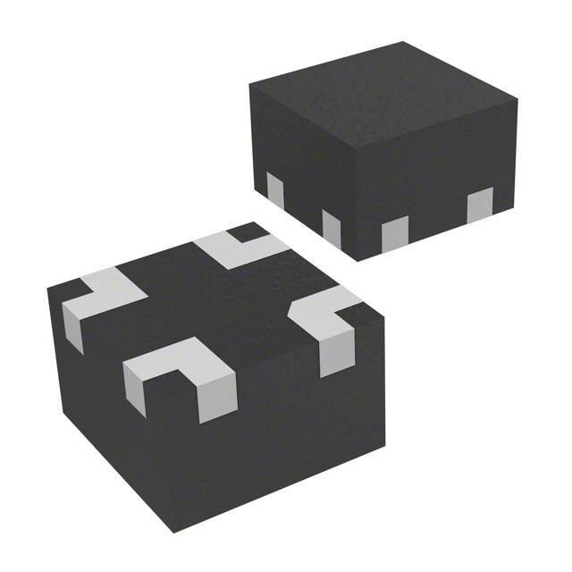
in 0.85 mm x 0.85 mm FTDFN Package
Features
General Description
• Space-Saving 0.85 mm x 0.85 mm 4-Lead
FTDFN Package
• Input Voltage Range: 1.7V to 5.5V
• 2A Continuous Operating Current
• 67 mΩ RDS(ON)
• Internal Level Shift for CMOS/TTL Control Logic
• Ultra-Low Quiescent Current
• Micropower Shutdown Current
• Soft-Start: MIC94082/3 (800 µs), MIC94084/5
(120 µs)
• Load Discharge Circuit: MIC94081, MIC94083,
MIC94085
• Ultra-Fast Turn-Off Time
• –40°C to +125°C Junction Operating Temperature
The MIC94080/1/2/3/4/5 is a family of high-side load
switches designed to operate from 1.7V to 5.5V input
voltage. The load switch pass element is an internal
67 mΩ RDS(ON) P-Channel MOSFET that enables the
device to support up to 2A of continuous current.
Additionally, the load switch supports 1.5V logic level
control and shutdown features in a tiny 0.85 mm x
0.85 mm 4-lead FTDFN package.
Applications
•
•
•
•
•
•
•
•
•
Cellular Phones
Portable Navigation Devices (PND)
Personal Media Players (PMP)
Ultra-Mobile PCs
Portable Instrumentation
Other Portable Applications
PDAs
GPS Modules
Industrial and Datacom Equipment
Package Type
MIC94080/1/2/3/4/5
4-Lead 0.85 mm x 0.85 mm FTDFN
(Top View)
2019 Microchip Technology Inc.
The MIC94080 and MIC94081 feature rapid turn on.
The MIC94082 and MIC94083 provide a slew rate
controlled soft-start turn-on of 800 μs, while the
MIC94084 and MIC94085 provide a slew rate
controlled soft-start turn-on of 120 μs. The soft-start
feature is provided to prevent an in-rush current event
from pulling down the input supply voltage.
The MIC94081, MIC94083, and MIC94085 feature an
active load discharge circuit which switches in a 250Ω
load when the switch is disabled to automatically
discharge a capacitive load.
An active pull-down on the enable input keeps the
MIC94080/1/2/3/4/5 in a default OFF state until the
enable pin is pulled above 1.25V. Internal level shift
circuitry allows low voltage logic signals to switch
higher supply voltages. The enable voltage can be as
high as 5.5V and is not limited by the input voltage.
The MIC94080/1/2/3/4/5 operating voltage range
makes
them
ideal
for
Lithium
ion
and
NiMH/NiCad/Alkaline battery powered systems, as well
as non-battery powered applications. The devices
provide low quiescent current and low shutdown
current to maximize battery life.
DS20006118A-page 1
�MIC94080/1/2/3/4/5
Typical Application Circuits
MIC94080 (Ultra-Fast Turn-On)
MIC94082 (800 µs Soft-Start)
MIC94084 (120 µs Soft-Start)
MIC94081 (Ultra-Fast Turn-On w/ Auto-Discharge)
MIC94083 (800 µs Soft-Start w/ Auto-Discharge)
MIC94085 (120 µs Soft-Start w/ Auto-Discharge)
VIN
VIN
EN
VOUT
VOUT
Level Shift
and Slew
Rate
Control
Load
EN
Level Shift
Slew Rate
Control
&
Load
Discharge
Load
GND
GND
DS20006118A-page 2
2019 Microchip Technology Inc.
�MIC94080/1/2/3/4/5
1.0
ELECTRICAL CHARACTERISTICS
Absolute Maximum Ratings †
Input Voltage (VIN) ......................................................................................................................................................+6V
Enable Voltage (VEN) ..................................................................................................................................................+6V
Continuous Drain Current (ID) (Note 1)
TA = +25°C............................................................................................................................................................... ±2.0A
TA = +85°C............................................................................................................................................................... ±1.5A
Pulsed Drain Current (IDP) (Note 2) ......................................................................................................................... ±6.0A
Continuous Diode Current (IS) (Note 3) ................................................................................................................–50 mA
Storage Temperature (TS)...................................................................................................................... –55°C to +150°C
ESD Rating (HBM, Note 4) ........................................................................................................................................ 3 kV
Operating Ratings ††
Input Voltage (VIN) .................................................................................................................................... +1.7V to +5.5V
Junction Temperature Range (TJ) .......................................................................................................... –40°C to +125°C
Package Thermal Resistance
4-Ld FTDFN 0.85 mm x 0.85 mm (JA)...............................................................................................................140°C/W
4-Ld FTDFN 0.85 mm x 0.85 mm (JC).................................................................................................................85°C/W
† Notice: Stresses above those listed under “Absolute Maximum Ratings” may cause permanent damage to the device.
This is a stress rating only and functional operation of the device at those or any other conditions above those indicated
in the operational sections of this specification is not intended. Exposure to maximum rating conditions for extended
periods may affect device reliability.
†† Notice: The device is not guaranteed to function outside its operating ratings.
Note 1: With thermal contact to PCB. See Thermal Considerations section.
2: Pulse width
很抱歉,暂时无法提供与“MIC94085YFT-TR”相匹配的价格&库存,您可以联系我们找货
免费人工找货- 国内价格
- 1+10.57090
- 10+7.04720
- 30+5.87270
- 国内价格
- 1+4.71960
- 10+4.62240
- 30+4.55760
- 国内价格 香港价格
- 1+5.397401+0.69824
- 25+4.6796325+0.60539
- 100+4.54361100+0.58779
- 国内价格 香港价格
- 5000+4.139555000+0.53552