MIC94090/1/2/3/4/5
High Side Load Switches for
Consumer Applications
General Description
Features
The MIC94090/1/2/3/4/5 is a family of high-side load switches
designed for operation from 1.7V to 5.5V input voltage. The
load switch pass element is an internal 130mΩ RDS(ON) Pchannel MOSFET which enables the device to support up to
1.2A continuous current. Additionally, the load switch
supports 1.5V logic level control and shutdown features.
The MIC94090 and MIC94091 feature rapid turn on. The
MIC94092 and MIC94093 provide a slew rate controlled softstart turn-on of 790µs, while the MIC94094 and MIC94095
provide a slew rate controlled soft-start turn-on of 120µs. The
soft-start feature option prevents an in-rush current event
from pulling down the input supply voltage.
The MIC94091, MIC94093, and MIC94095 include a 250Ω
auto discharge load circuit that is switched on when the load
switch is disabled.
An active pull-down on the enable input keeps the
MIC94090/1/2/3/4/5 in a default OFF state until the enable pin
is pulled above 1.25V. Internal level shift circuitry allows low
voltage logic signals to switch higher supply voltages. The
enable voltage can be as high as 5.5V and is not limited by
the input voltage.
The MIC94090/1/2/3/4/5 operating voltage range makes
them ideal for Lithium ion and NiMH/NiCad/Alkaline battery
powered systems, as well as non-battery powered
applications. The devices provide low quiescent current and
low shutdown current to maximize battery life.
Datasheets and support documentation can be found on
Micrel’s web site at: www.micrel.com.
•
•
•
•
•
•
•
•
•
•
1.7V to 5.5V input voltage range
1.2A continuous operating current
130mΩ RDS(ON)
Internal level shift for CMOS/TTL control logic
Ultra low quiescent current
Micro-power shutdown current
Rapid turn-on: MIC94090/1
Soft-Start: MIC94092/3 (790µs), MIC94094/5 (120µs)
Load discharge circuit: MIC94091/3/5
Space saving and thermally capable 1.2mm x 1.2mm
Thin MLF® package
• Industry standard SC-70-6 package
Applications
•
•
•
•
•
•
•
•
•
Cellular phones
Portable Navigation Devices (PND)
GPS modules
Personal Media Players (PMP)
Ultra Mobile PCs
Other Portable applications
PDAs
Portable instrumentation
Industrial and DataComm equipment
_________________________________________________________________________________________________________
Typical Application
MIC94090 (ultra fast turn on)
MIC94092 (790µs soft-start)
MIC94094 (120µs soft-start)
MIC94091 (ultra fast turn on with auto-discharge)
MIC94093 (790µs soft-start with auto-discharge)
MIC94095 (120µs soft-start with auto-discharge)
MLF and MicroLeadFrame are registered trademarks of Amkor Technology, Inc.
Micrel Inc. • 2180 Fortune Drive • San Jose, CA 95131 • USA • tel +1 (408) 944-0800 • fax + 1 (408) 474-1000 • http://www.micrel.com
March 2009
M9999-033109-A
�Micrel, Inc.
MIC94090/1/2/3/4/5
Ordering Information
Part Number
Pb-Free
Part Marking
(1)
Pb-Free
Fast
Turn On
SoftStart
MIC94090YMT
D1
●
MIC94091YMT
D2
●
MIC94092YMT
D5
790µs
MIC94093YMT
D7
790µs
MIC94094YMT
0D
120µs
MIC94095YMT
1D
120µs
MIC94090YC6
D1D
●
MIC94091YC6
D2D
●
MIC94092YC6
D5D
790µs
MIC94093YC6
D7D
790µs
MIC94094YC6
0DD
120µs
MIC94095YC6
1DD
120µs
Load
Discharge
Package(2)
(3)
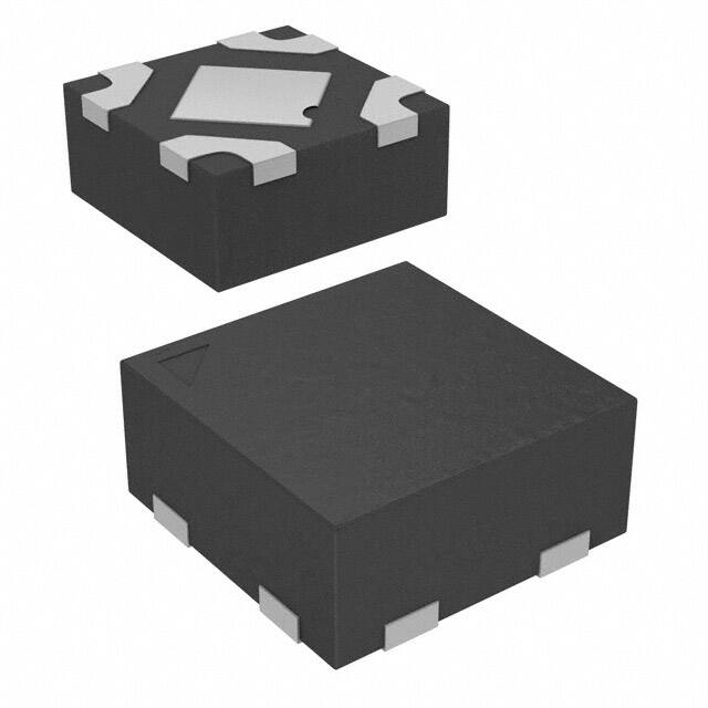
4-Pin 1.2mm x 1.2mm Thin MLF®
●
4-Pin 1.2mm x 1.2mm Thin MLF®
4-Pin 1.2mm x 1.2mm Thin MLF®
●
4-Pin 1.2mm x 1.2mm Thin MLF®
4-Pin 1.2mm x 1.2mm Thin MLF®
●
4-Pin 1.2mm x 1.2mm Thin MLF®
●
SC-70-6
SC-70-6
SC-70-6
●
SC-70-6
SC-70-6
●
SC-70-6
Notes:
1. Under bar symbol ( _ ) may not be to scale.
®
2. Thin MLF ▲ = Pin 1 identifier.
®
3. Thin MLF is a GREEN RoHS-compliant package. Lead finish is NiPdAu. Mold compound is Halogen Free.
Pin Configuration
PIN 1 TRIANGLE
BY MARKING
VOUT
1
4
GND
EN
2
3
VIN
4-Pin (1.2mm x 1.2mm) Thin MLF® (MT)
Top View
6-Pin SC-70-6 (C6)
Top View
Pin Description
Pin Number
Pin Name
Pin Function
TMLF-4
SC-70-6
1
1
VOUT
Drain of P-Channel MOSFET.
4
2, 5
GND
Ground: Connect to electrical ground.
3
4
VIN
Source of P-Channel MOSFET.
2
6
EN
Enable (Input): Active-high CMOS-compatible control input for switch. Internal 2MΩ
pull down resistor to GND, output will be off if this pin is left floating.
--
3
NC
No Internal Connection. A signal or voltage applied to this pin will have no effect on
device operation.
March 2009
2
M9999-033109-A
�Micrel, Inc.
MIC94090/1/2/3/4/5
Absolute Maximum Ratings(1)
Operating Ratings(2)
Input Voltage (VIN) ...................................................... +6V
Enable Voltage (VEN) ................................................. +6V
Continuous Drain Current (ID)(3)
TA = 25°C (MLF®).............................................. ±1.2A
TA = 25°C (SC-70) ............................................ ±1.2A
Pulsed Drain Current (IDP)(4) .................................... ±6.0A
Continuous Diode Current (IS)(5) ............................ –50mA
Storage Temperature (Ts) ..................... –55°C to +150°C
ESD Rating – HBM(6)...................................................3kV
Input Voltage (VIN)....................................... +1.7 to +5.5V
Junction Temperature (TJ) .....................–40°C to +125°C
Package Thermal Resistance
Thin MLF® (θJC)(3) ............................................60°C/W
Thin MLF® (θJA)(3) ..........................................140°C/W
SC-70-6 (θJC) ................................................100°C/W
SC-70-6 (θJA) ................................................240°C/W
Electrical Characteristics
TA = 25°C, bold values indicate –40°C< TA < +85°C, unless noted.
Symbol
Parameter
Condition
Min
0.4
VEN_TH
Enable Threshold Voltage
VIN = 1.7V to 4.5V, ID = –250μA
IQ
Quiescent Current Measured on
the VIN Pin
VIN = VEN = 5.5V, ID = OPEN
Measured on VIN MIC94090/1
VIN = VEN = 5.5V, ID = OPEN
Measured on VIN MIC94092/3/4/5
Typ
Max
Units
1.25
V
0.1
1
µA
8
15
µA
IEN
Enable Input Current
VIN = VEN = 5.5V, ID = OPEN
2.5
4
µA
ISD
Shutdown Current
VIN = +5.5V, VEN = 0V, ID = OPEN
Measured on the VIN pin(7)
0.01
1
µA
ISHUT-SWITCH
OFF State Leakage Current
VIN = +5.5V, VEN = 0V, ID = SHORT
Measured on VOUT(7)
0.01
1
µA
RDS(ON)
P-Channel Drain to Source ON
Resistance
VIN = +5.0V, ID = –100mA, VEN = 1.5V
130
225
mΩ
VIN = +4.5V, ID = –100mA, VEN = 1.5V
135
235
mΩ
VIN = +3.6V, ID = –100mA, VEN = 1.5V
140
255
mΩ
VIN = +2.5V, ID = –100mA, VEN = 1.5V
170
315
mΩ
VIN = +1.8V, ID = –100mA, VEN = 1.5V
235
355
mΩ
VIN = +1.7V, ID = –100mA, VEN = 1.5V
260
375
mΩ
VIN = +3.6V, ITEST = 1mA, VEN = 0V
MIC94091/3/5
250
400
Ω
RSHUTDOWN
March 2009
Turn-Off Resistance
3
M9999-033109-A
�Micrel, Inc.
MIC94090/1/2/3/4/5
Electrical Characteristics (Dynamic)
TA = 25°C, bold values indicate –40°C< TA < +85°C, unless noted.
Symbol
Parameter
Condition
tON_DLY
Turn-On Delay Time
VIN = +3.6V, ID = –100mA, VEN = 1.5V
Min
Typ
Max
Units
0.4
1.5
µs
200
740
1500
µs
65
110
165
µs
0.4
1.5
µs
400
790
1500
µs
65
120
175
µs
MIC94090/1
VIN = +3.6V, ID = –100mA, VEN = 1.5V
MIC94092/3
VIN = +3.6V, ID = –100mA, VEN = 1.5V
MIC94094/5
tON_RISE
Turn-On Rise Time
VIN = +3.6V, ID = –100mA, VEN = 1.5V
MIC94090/1
VIN = +3.6V, ID = –100mA, VEN = 1.5V
MIC94092/3
VIN = +3.6V, ID = –100mA, VEN = 1.5V
MIC94094/5
tOFF_DLY
Turn-Off Delay Time
VIN = +3.6V, ID = –100mA, VEN = 1.5V
60
200
ns
tOFF_FALL
Turn-Off Fall Time
VIN = +3.6V, ID = –100mA, VEN = 1.5V
10
100
ns
Notes:
1. Exceeding the absolute maximum rating may damage the device.
2. The device is not guaranteed to function outside its operating rating.
3. With backside thermal contact to PCB. See thermal considerations section.
4. Pulse width