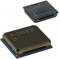
MICRF600
902-928MHz ISM Band Transceiver
Module
General Description
The MICRF600 is a self-contained frequency shift keying (FSK)
transceiver module, intended for use in half-duplex, bidirectional
RF links. The multi-channeled FSK transceiver module is intended
for UHF radio equipment in compliance with the North American
Federal Communications Commission (FCC) part 15.247 and
249.
The transmitter consists of a fully programmable PLL frequency
synthesizer and power amplifier. The frequency synthesizer
consists of a voltage-controlled oscillator (VCO), a crystal
oscillator, dual modulus prescaler, programmable frequency
dividers, and a phase-detector. The output power of the power
amplifier can be programmed to seven levels. A lock-detect circuit
detects when the PLL is in lock.
In receive mode, the PLL synthesizer generates the local oscillator
(LO) signal. The N, M, and A values that give the LO frequency
are stored in the N0, M0, and A0 registers.
The receiver is a zero intermediate frequency (IF) type that makes
channel filtering possible with low-power, integrated low-pass
filters. The receiver consists of a low noise amplifier (LNA) that
drives a quadrature mix pair. The mixer outputs feed two identical
signal channels in phase quadrature. Each channel includes a
pre-amplifier, a third order Sallen-Key RC low-pass filter that
protects the following switched-capacitor filter from strong adjacent
channel signals, and a limiter. The main channel filter is a
switched-capacitor implementation of a six-pole elliptic low pass
filter. The cut-off frequency of the Sallen-Key RC filter can be
programmed to four different frequencies: 100kHz, 150kHz,
230kHz, and 350kHz. The I and Q channel outputs are
demodulated and produce a digital data output. The demodulator
detects the relative phase of the I and the Q channel signal. If the I
channel signal lags behind the Q channel, the FSK tone
frequency is above the LO frequency (data “1”). If the I channel
leads the Q channel, then the FSK tone is below the LO
frequency (data “0”). The output of the receiver is available on the
DataIXO pin. A receive signal strength indicator (RSSI) circuit
indicates the received signal level. All support documentation can
be found on Micrel’s web site at: www.micrel.com.
RadioWire® Module
Features
•
•
•
•
•
•
•
•
•
•
•
•
“Drop in” RF solution
Small size: 11.5x14.1mm
RF tested
FCC Compliant
Low Power
Surface Mountable
Tape & Reel
Digital Bit Synchronizer
Received Signal Strength Indicator (RSSI)
RX and TX power management
Power down function
Register read back function
Applications
•
•
•
•
•
•
•
Telemetry
Remote metering
Wireless controller
Remote data repeater
Remote control systems
Wireless modem
Wireless security system
RadioWire® is a trademark of Micrel, Inc
Micrel Inc. • 2180 Fortune Drive • San Jose, CA 95131 • USA • tel +1 (408) 944-0800 • fax + 1 (408) 474-1000 • http://www.micrel.com
July 2006
M9999-082505
�Micrel, Inc.
MICRF600/MICRF600Z
Contents
General Description ................................................................................................................................................................ 1
Features .................................................................................................................................................................................. 1
Applications ............................................................................................................................................................................. 1
Contents .................................................................................................................................................................................. 2
RadioWire® RF Module Selection Guide................................................................................................................................. 3
Ordering Information ............................................................................................................................................................... 3
Block Diagram ......................................................................................................................................................................... 3
Pin Configuration..................................................................................................................................................................... 4
Pin Description ........................................................................................................................................................................ 4
Absolute Maximum Ratings(1) ................................................................................................................................................. 5
Operating Ratings(2) ................................................................................................................................................................ 5
Electrical Characteristics......................................................................................................................................................... 5
Programming........................................................................................................................................................................... 7
General ............................................................................................................................................................................... 7
Writing to the Control Registers in MICRF600 ................................................................................................................... 8
Writing to a Single Register ................................................................................................................................................ 8
Writing to All Registers ....................................................................................................................................................... 8
Writing to n Registers Having Incremental Addresses ....................................................................................................... 9
Reading from the Control Registers in MICRF600 ............................................................................................................. 9
Reading n Registers from MICRF600................................................................................................................................. 9
Programming Interface Timing.............................................................................................................................................. 10
Power on Reset ................................................................................................................................................................ 11
Programming Summary.................................................................................................................................................... 11
Frequency Synthesizer ......................................................................................................................................................... 12
Crystal Oscillator (XCO) ................................................................................................................................................... 12
VCO .................................................................................................................................................................................. 12
Lock Detect ....................................................................................................................................................................... 13
Modes of Operation............................................................................................................................................................... 13
Transceiver Sync/Non-Synchronous Mode ...................................................................................................................... 14
Data Interface ................................................................................................................................................................... 14
Receiver ................................................................................................................................................................................ 14
Front End .......................................................................................................................................................................... 15
Sallen-Key Filters.............................................................................................................................................................. 15
Switched Capacitor Filter.................................................................................................................................................. 15
RSSI.................................................................................................................................................................................. 15
FEE ................................................................................................................................................................................... 16
Bit Synchronizer................................................................................................................................................................ 16
Transmitter ............................................................................................................................................................................ 18
Power Amplifier................................................................................................................................................................. 18
Frequency Modulation ...................................................................................................................................................... 18
Using the XCO-tune Bits ....................................................................................................................................................... 18
Application Circuit Illustration ................................................................................................................................................ 19
Assembling the MICRF600 ................................................................................................................................................... 19
Recommended Reflow Temperature Profile .................................................................................................................... 19
Shock/Vibration during Reflow.......................................................................................................................................... 19
Handassembling the MICRF600....................................................................................................................................... 19
Layout.................................................................................................................................................................................... 20
Recommended Land Pattern............................................................................................................................................ 20
Layout Considerations ...................................................................................................................................................... 20
Package Dimensions ............................................................................................................................................................ 21
Tape Dimensions .................................................................................................................................................................. 21
July 2006
2
M9999-082505
�Micrel, Inc.
MICRF600/MICRF600Z
RadioWire® RF Module Selection Guide
Device
MICRF600
Frequency
Range
Data Rate
Receive
Supply
Voltage
Transmit
Modulation
Type
Package
902-928 MHz
-129 = +127
2) 126
For all other combinations the PA is on and has maximum
power when PA2 – PA0 = 1.
The PA will be bypassed if PA_by=1. Output power will
drop ~14dB. It is still possible to control the power by PA2
– PA0.
July 2006
3) 125
To avoid this situation, always make sure max count is
between limits.
18
M9999-082505
�Micrel, Inc.
MICRF600/MICRF600Z
Application Circuit Illustration
Assembling the MICRF600
Recommended Reflow Temperature Profile
When the MICRF600 module is being automatically
assembled to a PCB, care must be taken not to expose
the module for temperature above the maximum specified.
Figure 13 shows the recommended reflow temperature
profile.
LDO
MCU
MICRF600
4004
Figure 11. Circuit illustration of MICRF600, LDO and MCU
Figure 11. shows a typical set-up with the MICRF600, a
Low-Drop-Out voltage regulator (LDO) and a mikrocontroller (MCU). When the MICRF600 and the MCU runs
on the same power supply (min 2.0, max. 2.5V), the IO
can be connected directly to the MCU. If the MCU needs a
higher VDD than the max. specified VDD of the MICRF600
(2.5V), voltage dividers need to be added on the IO lines
not to override the max. input voltage.
Figure 12 shows a recommended voltage divider circuit for
a MCU running at 3.0V and the MICRF600 at 2.5V.
MICRF6xx
MCU
3k3
CS
CS
18k
3k3
SCLK
3k3
IO
IO
18k
15k
DATAIXO
DATAIXO
DATACLK
DATACLK
RSSI
Shock/Vibration during Reflow
The module has several components inside which are
assembled in a reflow process. These components may
reflow again when the module is assembled onto a PCB. It
is therefore important that the module is not subjected to
any mechanical shock or vibration during this process.
SCLK
18k
LD
Figure 13. Recommended Reflow Temperature Reflow
Handassembling the MICRF600
It is recommended to use solder paste also during hand
assembling of the module. Because of the module ground
pad on the bottom side, the module will be assembled
most efficient if the heat is being subjected to the bottom
side of the PCB. The heat will be transferred trough the
PCB due the ground vias under the module (see Layout
Considerations). In addition, it is recommended to use a
solder tip on the signal and power pads, to make sure the
solder points are properly melted.
LD
RSSI
Figure 12. How to connect MCU600 (2.5V) and MCU (3.0V)
July 2006
19
M9999-082505
�Micrel, Inc.
Layout
Recommended Land Pattern
Figure 14 shows a recommended land pattern that
facilitates both automatic and hand assembling.
MICRF600/MICRF600Z
Layout Considerations
Except for the antenna input/output signal, only digital and
low frequency signals need to interface with the module.
There is therefore no need of years of RF expertise to do a
successful layout, as long as the following few points are
being followed:
•
Proper ground is needed. If the PCB is 2-layer, the
bottom layer should be kept only for ground. Avoid
signal traces that split the ground plane. For a 4layer PCB, it is recommended to keep the second
layer only for ground.
•
A ground via should be placed close to all the
ground pins. The bottom ground pad should be
penetrated with 4-16 ground vias.
•
The antenna has a impedance of ~50 ohm. The
antenna trace should be kept to 50 ohm to avoid
signal reflection and loss of performance. Any
transmission line calculator can be used to find the
needed trace width given a board build up. Ex: A
trace width of 44 mil (1.12 mm) gives 50
impedance on a FR4 board (dielectric cons=4.4)
with copper thickness of 35µm and height (layer 1layer 2 spacing) of 0.61 mm.
•
RF circuitry is sensitive to voltage supply and
therefore caution should be taken when choosing
power circuitry. To achieve the best performance,
low noise LDO’s with high PSSR should be
chosen. What is present on the voltage supply will
be directly modulated to the RF spectrum causing
degradation and regulatory issues. To make sure
you have the right selection, please contact local
sales for the latest Micrel offerings in power
management and guidance. To avoid “pickup”
from other circuitry on the VDD lines, it is
recommended to route the VDD in a star
configuration with decoupling at each circuitry and
at the common connection point (see above
layout). If there are noisy circuitry in the design, it
is strongly recommended to use a separate power
supply and/or place low value resistors (10ohms),
inductors in series with the power supply line into
these circuitry.
•
Digital high speed logic or noisy circuitry
should/must be at a safe distance from RF
circuitry or RF VDD as this might/will cause
degradation of sensitivity and create spurious
emissions. Example of such circuitry is LCD
display, charge pumps, RS232, clock / data bus
etc.
Figure 14. Recommended Land Pattern
July 2006
20
M9999-082505
�Micrel, Inc.
MICRF600/MICRF600Z
Package Dimensions
Figure 15. Package Dimensions
Tape Dimensions
Figure 16. Tape Dimensions
MICREL, INC. 2180 FORTUNE DRIVE SAN JOSE, CA 95131 USA
TEL +1 (408) 944-0800 FAX +1 (408) 474-1000 WEB http:/www.micrel.com
The information furnished by Micrel in this data sheet is believed to be accurate and reliable. However, no responsibility is assumed by Micrel for its
use. Micrel reserves the right to change circuitry and specifications at any time without notification to the customer.
Micrel Products are not designed or authorized for use as components in life support appliances, devices or systems where malfunction of a product
can reasonably be expected to result in personal injury. Life support devices or systems are devices or systems that (a) are intended for surgical implant
into the body or (b) support or sustain life, and whose failure to perform can be reasonably expected to result in a significant injury to the user. A
Purchaser’s use or sale of Micrel Products for use in life support appliances, devices or systems is a Purchaser’s own risk and Purchaser agrees to fully
indemnify Micrel for any damages resulting from such use or sale.
© 2005 Micrel, Incorporated.
July 2006
21
M9999-082505
�