PL360
PL360 Datasheet
Description
The PL360 is a programmable modem for narrow-band Power Line Communication (PLC), able to run any PLC
protocol in the frequency band below 500 kHz.
This device has been designed to comply with FCC, ARIB, KN60 and CENELEC EN50065 regulations matching
requirements of Internet of Things and Smart Energy applications. It supports state-of-the-art narrow-band PLC
standards such as ITU G.9903 (G3-PLC®), ITU G.9904 (PRIME) as well as any other narrowband PLC protocols,
being at the same time a future-proof platform able to support the evolution of these standards.
The PL360 has been conceived to be driven by external Microchip host devices, thus providing an additional level of
flexibility on the host side. The Microchip host device loads the proper PLC-protocol firmware before modem
operation and controls the PL360 modem.
Features
•
•
•
•
•
•
•
Programmable Narrow-Band Power Line Communication (PLC) Modem
Integrated PLC Front End:
– PGA with automatic gain control and ADC
– DAC and transmission driver supports direct line driving or external Class-D amplifier driving
– Digital transmission level control
– Supports two independent transmission branches for the PLC signal
– Up to 500 kHz PLC signal bandwidth
Architecture
– High performance architecture combining CPU, specific co-processors for digital signal processing and
dedicated hardware accelerators for common narrow-band PLC tasks
– Dedicated SRAM memories for code and data
®
®
ARM 32-bit Cortex -M7 Core Managing PL360 System: Co-Processors, Hardware Accelerators and
Peripherals
– 216 MHz maximum frequency
– 192 kB of SRAM for data and code
– Bootloader allows loading plain programs or authenticated and encrypted programs
– 12 multiplexed GPIOs
– 1 SPI, 1 UART, 2 PWM
– Serial wire debug port
– Zero-Crossing Detection on the mains
Cryptographic Engine and Secure Boot
– AES 128, 192, 256 supported
– Secure boot: supports AES-128 CMAC for authentication, AES-128 CBC for decryption
– Fuse programming control for decryption and authentication 128-bit keys
Clock Management
– 24 MHz external crystal for system clock
Power Management
© 2019 Microchip Technology Inc.
Datasheet
DS70005364C-page 1
�PL360
•
•
– 3.3 V external supply voltage for I/O, digital and analog
– 1.25 V internal voltage regulator for the core
– Optimized power modes for specific operation profiles, including Low Power mode
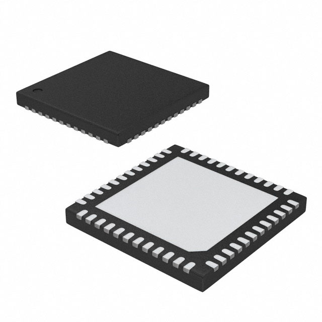
Available in TQFP-48 and QFN-48 Packages
-40ºC to +85ºC Temperature Range
© 2019 Microchip Technology Inc.
Datasheet
DS70005364C-page 2
�PL360
Table of Contents
Description..................................................................................................................................................... 1
Features......................................................................................................................................................... 1
1.
PL360 Application Block Diagram...........................................................................................................5
2.
Block Diagram.........................................................................................................................................6
3.
Signal Description................................................................................................................................... 7
4.
Package and Pinout................................................................................................................................ 9
4.1.
4.2.
4.3.
4.4.
4.5.
5.
Analog Front-End.................................................................................................................................. 13
5.1.
5.2.
6.
General-Purpose I/O Lines.........................................................................................................18
System I/O Lines........................................................................................................................ 18
Bootloader.............................................................................................................................................19
8.1.
8.2.
8.3.
8.4.
9.
Power Supplies.......................................................................................................................... 16
Power Constraints...................................................................................................................... 16
Input/Output Lines.................................................................................................................................18
7.1.
7.2.
8.
PLC Coupling Circuitry Description............................................................................................ 13
Coupling Reference Designs......................................................................................................15
Power Considerations........................................................................................................................... 16
6.1.
6.2.
7.
48–Lead TQFP Package Outline................................................................................................. 9
48–Lead TQFP Pinout..................................................................................................................9
48–Lead QFN Package Outline................................................................................................... 9
48–Lead QFN Pinout..................................................................................................................10
Pinout Specification....................................................................................................................10
Description................................................................................................................................. 19
Embedded Characteristics......................................................................................................... 19
Block Diagram............................................................................................................................ 19
Functional Description................................................................................................................20
Serial Peripheral Interface (SPI)........................................................................................................... 27
9.1.
9.2.
9.3.
9.4.
Description................................................................................................................................. 27
Embedded Characteristics......................................................................................................... 27
Signal Description...................................................................................................................... 27
Functional Description................................................................................................................27
10. Transmission Path.................................................................................................................................30
10.1.
10.2.
10.3.
10.4.
Description................................................................................................................................. 30
Embedded Characteristics......................................................................................................... 30
Block Diagram............................................................................................................................ 30
Product Dependencies............................................................................................................... 30
11. Reception Path......................................................................................................................................32
11.1. Description................................................................................................................................. 32
© 2019 Microchip Technology Inc.
Datasheet
DS70005364C-page 3
�PL360
11.2. Embedded Characteristics......................................................................................................... 32
11.3. Block Diagram............................................................................................................................ 32
11.4. Functional Description................................................................................................................32
12. Advanced Encryption Standard (AES).................................................................................................. 36
12.1. Description................................................................................................................................. 36
13. Electrical Characteristics.......................................................................................................................37
13.1.
13.2.
13.3.
13.4.
13.5.
13.6.
13.7.
13.8.
Absolute Maximum Ratings........................................................................................................37
Recommended Operating Conditions........................................................................................ 37
Electrical Pinout..........................................................................................................................38
DC Characteristics..................................................................................................................... 39
Power Consumption................................................................................................................... 40
Crystal Oscillator........................................................................................................................ 41
PGA and ADC............................................................................................................................ 41
Power On Considerations.......................................................................................................... 42
14. Mechanical Characteristics................................................................................................................... 43
14.1. TQFP48 Mechanical Characteristics..........................................................................................43
14.2. QFN48 Mechanical Characteristics............................................................................................44
15. Recommended Mounting Conditions.................................................................................................... 45
15.1. Conditions of Standard Reflow...................................................................................................45
15.2. Manual Soldering....................................................................................................................... 46
16. Marking................................................................................................................................................. 47
17. Ordering Information............................................................................................................................. 48
18. Revision History.................................................................................................................................... 49
18.1. Rev A - 06/2018......................................................................................................................... 49
18.2. Rev B - 01/2019......................................................................................................................... 49
18.3. Rev C - 08/2019......................................................................................................................... 49
The Microchip Website.................................................................................................................................50
Product Change Notification Service............................................................................................................50
Customer Support........................................................................................................................................ 50
Microchip Devices Code Protection Feature................................................................................................ 50
Legal Notice................................................................................................................................................. 50
Trademarks.................................................................................................................................................. 51
Quality Management System....................................................................................................................... 51
Worldwide Sales and Service.......................................................................................................................52
© 2019 Microchip Technology Inc.
Datasheet
DS70005364C-page 4
�PL360
PL360 Application Block Diagram
1.
PL360 Application Block Diagram
PL360 transceiver has been conceived to be easily managed by an external microcontroller through a 4-line standard
Serial Peripheral Interface (SPI). By means of the SPI, the external microcontroller can fully manage and control the
PL360 by accessing the internal peripheral registers.
Two additional signals are used by the host to control the PL360: LDO enable and NRST.
Some GPIOs can be used as interrupt signals from the PL360 to the external microcontroller depending on the
requirements of the protocol being used.
Figure 1-1. PL360 Application Example
L
N
PL360
Power
Supply
NPCS0 / PA6
SPCK / PA7
External
Microcontroller
MOSI / PA8
MISO / PA9
EMIT [0:3]
PA11 / TXRX1
PA10 / TXRX0
VIN
LDO Enable
PLC
Coupling
AGC
NRST
PA12 / VZC (2)
Ext. Interr.
Zero-Crossing
External Circuit
Carrier Detect Interr. (1)
Notes:
1. Used by protocols requiring carrier detection signaling
2. Used by applications requiring phase detection
© 2019 Microchip Technology Inc.
Datasheet
DS70005364C-page 5
�PL360
Block Diagram
Block Diagram
Figure 2-1. PL360 Block Diagram
SWCLK
SWDIO
TRACESWO
ITCM
DEBUG
TRACE
CPU
AXIM
DTCM
DTCM
SRAM
AHBS
SIGNAL
PROCESSING
UNIT
AHBP
AXI
BRIDGE
BUS MATRIX
VIN
VREFP
VREFC
VREFN
AGC
DMA
DMA
RX
PATH
TX
PATH
VZC
EMITx
TXRXx
PERIPHERALS
BOOTLOADER
CONTROL
PA
PC
S
SP 0
C
M K
O
S
M I
IS
O
x
SPI
SPI
XIN
XOUT
LDO ENABLE
NRST
N
2.
© 2019 Microchip Technology Inc.
Datasheet
DS70005364C-page 6
�PL360
Signal Description
3.
Signal Description
Table 3-1. Signal Description List
Signal Name
Function
Type
Active
Level
Voltage
reference
Comments
Power Supplies
VDDIO
3.3V Digital supply. Digital power supply must be
decoupled by external capacitors
Power
3.0V to 3.6V
VDDIN
3.3V Voltage Regulator Input
Power
3.0V to 3.6V
VDDIN_AN
3.3V Analog supply (ADC + PGA)
Power
3.0V to 3.6V
VDDCORE
1.25V Voltage Regulator Output with internal
connection to Core power supply. Decoupling
capacitors must be placed in VDDCORE pins
Power
1.25V
VDDPLL
1.25V PLL power supply input. Must be
connected to pin 7 (VDDCORE) through a LP
filter
Power
1.25V
GND
Digital Ground
Power
(1)
AGND
Analog Ground
Power
(1)
Clocks, Oscillators and PLLs
XIN
Crystal Oscillator Input
XOUT
Crystal Oscillator Output
Input
VDDIO
Output
VDDIO
Reset/Test
NRST
System Reset
Input
Low
VDDIO
TST
Test Mode
Input
High
VDDIO
LDO ENABLE Enable Internal LDO regulator
Input
Power Line Communications
EMIT [0:3]
PLC Tri-state Transmission ports
VIN
PLC signal reception input
Output
VDDIO
Input
VDDIN_AN
Automatic Gain Control:
•
AGC
This digital tri-state output is managed by
AGC hardware logic to drive external Output
circuitry when input signal attenuation is
needed
VDDIO
(3)
VDDIO
External Protection
Resistor (2) (3)
Mains Zero-Cross Detection Signal:
VZC
•
This input detects the zero-crossing of the
mains voltage
© 2019 Microchip Technology Inc.
Input
Datasheet
DS70005364C-page 7
�PL360
Signal Description
Analog Front-End Transmission/Reception for
TXDRV0
TXRX0
•
This digital output is used to modify Output
external coupling behavior in Transmission/
Reception
VDDIO
Analog Front-End Transmission/Reception for
TXDRV1
•
TXRX1
This digital output is used to modify
external coupling behavior in Transmission/
Output
Reception. The suitable value depends on
the external circuitry configuration. The
polarity of this pin can be inverted by
software
VDDIO
VREFP
Internal Reference “Plus” Voltage. Bypass to
analog ground with an external decoupling
capacitor. Connect an external decoupling
capacitor between VREFP and VREFN.
Analog
VDDIN_AN
VREFN
Internal Reference “Minus” Voltage. Bypass to
analog ground with an external decoupling
capacitor. Connect an external decoupling
capacitor between VREFP and VREFN.
Analog
VDDIN_AN
VREFC
Internal Reference Common-mode Voltage.
Bypass to analog ground with an external
decoupling capacitor.
Analog
VDDIN_AN
General Purpose I/Os
PA [0:11]
General Purpose Input / Output
PA [12]
General Purpose Input
I/O
VDDIO
(4)
Input
VDDIO
(4)
Serial Wire - Debug Port – SW-DP
SWDIO
Serial Wire Input/Output
SWCLK
Serial Wire Clock
TRACESWO
Trace Asynchronous Data Out
I/O
VDDIO
Input
VDDIO
Output
VDDIO
Serial Peripheral Interface - SPI
VDDIO
Internal pull up (4)
Input
VDDIO
Internal pull up (4)
SPI Master Out Slave In
Input
VDDIO
Internal pull up (4)
SPI Master In Slave Out
Output
VDDIO
NPCS
SPI Chip Select
Input
SPCK
SPI Clock signal
MOSI
MISO
Low
Notes:
1.
2.
3.
4.
Separate pins are provided for GND and AGND grounds. Layout considerations should be taken into account
to reduce interference. Ground pins should be connected as short as possible to the system ground plane. For
more details about EMC Considerations, please refer to AVR040 application note
Depending on whether an isolated or a non-isolated power supply is being used, isolation of this pin should be
taken into account in the circuitry design. Please refer to the Reference Design for further information
See Table 13-4
See Table 13-5
© 2019 Microchip Technology Inc.
Datasheet
DS70005364C-page 8
�PL360
Package and Pinout
4.
Package and Pinout
4.1
48–Lead TQFP Package Outline
The 48-lead TQFP package has a 0.5 mm pitch and respects Green standards.
Figure 4-1 shows the orientation of the 48-lead TQFP package. Refer to the section 14. Mechanical Characteristics
for the 48-lead TQFP package mechanical drawing.
Figure 4-1. Orientation of the 48-Lead TQFP Package
36
25
37
24
48
13
1
4.2
12
48–Lead TQFP Pinout
Table 4-1. 48 - Lead TQFP Pinout
4.3
1
NRST
13
PA0
25
EMIT1
37
GND
2
XIN
14
PA1
26
VDDIO
38
AGND
3
XOUT
15
PA2/TRACESWO
27
EMIT2
39
VIN
4
VDDIO
16
PA3
28
VDDIO
40
VDDIN_AN
5
VDDPLL
17
PA6/NPCS0
29
VDDCORE
41
VREFP
6
GND
18
PA7/SPCK
30
GND
42
VREFC
7
VDDCORE
19
PA8/MOSI
31
EMIT3
43
VREFN
8
VDDIN
20
PA9/MISO
32
VDDIO
44
AGND
9
LDO ENABLE
21
VDDIO
33
PA11/TXRX1
45
VDDIN_AN
10
PA4/SWDIO
22
GND
34
PA10/TXRX0
46
VDDIO
11
PA5/SWCLK
23
EMIT0
35
AGC
47
PA12/VZC
12
VDDIO
24
VDDIO
36
VDDIO
48
TST
48–Lead QFN Package Outline
The 48-lead QFN package has a 0.4 mm pitch and respects Green standards.
Figure 4-1 shows the orientation of the 48-lead QFN package. Refer to the section 14. Mechanical Characteristics
for the 48-lead QFN package mechanical drawing.
© 2019 Microchip Technology Inc.
Datasheet
DS70005364C-page 9
�PL360
Package and Pinout
Figure 4-2. Orientation of the 48-Lead QFN Package
36
25
24
37
0
GND
13
48
1
4.4
12
48–Lead QFN Pinout
Table 4-2. 48 - Lead QFN Pinout
0
4.5
GND
1
NRST
13
PA0
25
EMIT1
37
GND
2
XIN
14
PA1
26
VDDIO
38
AGND
3
XOUT
15
PA2/TRACESWO
27
EMIT2
39
VIN
4
VDDIO
16
PA3
28
VDDIO
40
VDDIN_AN
5
VDDPLL
17
PA6/NPCS0
29
VDDCORE
41
VREFP
6
GND
18
PA7/SPCK
30
GND
42
VREFC
7
VDDCORE
19
PA8/MOSI
31
EMIT3
43
VREFN
8
VDDIN
20
PA9/MISO
32
VDDIO
44
AGND
9
LDO ENABLE
21
VDDIO
33
PA11/TXRX1
45
VDDIN_AN
10
PA4/SWDIO
22
GND
34
PA10/TXRX0
46
VDDIO
11
PA5/SWCLK
23
EMIT0
35
AGC
47
PA12/VZC
12
VDDIO
24
VDDIO
36
VDDIO
48
TST
Pinout Specification
Table 4-3. Pinout Specification
Primary
Pin
Power Rail
I/O Type
1
VDDIO
2
PIO Peripheral A
Dir
RST
NRST
I
I, Hiz
VDDIO
CLOCK
XIN
I
I, Hiz
3
VDDIO
CLOCK
XOUT
O
O
4
VDDIO
Power
VDDIO
-
5
VDDPLL
Power
VDDPLL
-
6
GNDOSC
Power
GNDOSC
-
Datasheet
Dir
Signal, Dir, Hiz,
ST
Signal
© 2019 Microchip Technology Inc.
Signal
Reset State
DS70005364C-page 10
�PL360
Package and Pinout
...........continued
Primary
Pin
Power Rail
I/O Type
7
VDDCORE
8
PIO Peripheral A
Dir
Power
VDDCORE
-
VDDIN
Power
VDDIN
-
9
VDDIO
LDO
LDO
ENABLE
I
10
VDDIO
GPIO
PA4
I/O
SWDIO
I/O
SWDIO, I, Hiz
11
VDDIO
GPIO
PA5
I/O
SWCLK
I
SWCLK, I, Hiz
12
VDDIO
Power
VDDIO
-
13
VDDIO
GPIO
PA0
I/O
PIO, I, Hiz
14
VDDIO
GPIO
PA1
I/O
PIO,I, Hiz
15
VDDIO
GPIO
PA2
I/O
16
VDDIO
GPIO
PA3
I/O
17
VDDIO
GPIO
PA6
I/O
NPCS0
I
NPCS0, I, Hiz
18
VDDIO
GPIO
PA7
I/O
SPCK
I
SPCK, I, Hiz
19
VDDIO
GPIO
PA8
I/O
MOSI
I
MOSI, I, Hiz
20
VDDIO
GPIO
PA9
I/O
MISO
O
MISO, O, ST1
21
VDDIO
Power
VDDIO
-
22
GND
Power
GND
-
23
VDDIO
PLC
EMIT0
O
24
VDDIO
Power
VDDIO
-
25
VDDIO
PLC
EMIT1
O
26
VDDIO
Power
VDDIO
-
27
VDDIO
PLC
EMIT2
O
28
VDDIO
Power
VDDIO
-
29
VDDCORE
Power
VDDCORE
-
30
GND
Power
GND
-
31
VDDIO
PLC
EMIT3
O
32
VDDIO
Power
VDDIO
-
33
VDDIO
GPIO
PA11
I/O
TXRX1
O
PIO, I, Hiz
34
VDDIO
GPIO
PA10
I/O
TXRX0
O
PIO, I, Hiz
35
VDDIO
AGC
AGC
O
36
VDDIO
Power
VDDIO
-
37
GND
Power
GND
-
38
AGND
Ground
AGND
-
39
VDDIN_AN
PLC
VIN
I
Datasheet
Dir
Signal, Dir, Hiz,
ST
Signal
© 2019 Microchip Technology Inc.
Signal
Reset State
I, Hiz
TRACESWO
O
PIO, I, Hiz
PIO, I, Hiz
O, Hiz
O, Hiz
O, Hiz
O, Hiz
O, ST0
I, Hiz
DS70005364C-page 11
�PL360
Package and Pinout
...........continued
Primary
Pin
Power Rail
I/O Type
40
VDDIN_AN
41
PIO Peripheral A
Signal
Dir
Power
VDDIN_AN
-
VDDIN_AN
Analog
VREFP
-
42
VDDIN_AN
Analog
VREFC
-
43
VDDIN_AN
Analog
VREFN
-
44
AGND
Ground
AGND
-
45
VDDIN_AN
Power
VDDIN_AN
-
46
VDDIO
Power
VDDIO
-
47
VDDIO
GPIO
VZC/PA12
I
48
VDDIO
TST
TST
I
Signal
Dir
Reset State
Signal, Dir, Hiz,
ST
VZC/PIO, I, Hiz
Note:
HiZ = High Impedance, ST = Set To.
© 2019 Microchip Technology Inc.
Datasheet
DS70005364C-page 12
�PL360
Analog Front-End
5.
Analog Front-End
5.1
PLC Coupling Circuitry Description
Microchip PLC technology is purely digital and does not require external DAC/ADC, thus simplifying the external
required circuitry. Generally, Microchip PLC coupling reference designs make use of few passive components plus a
Class D amplification stage for transmission.
All PLC coupling reference designs are generally composed by the same sub-circuits:
•
•
•
•
Transmission Stage
Reception Stage
Filtering Stage
Coupling Stage
Figure 5-1. PLC Coupling Block Diagram
RECEPTION
STAGE
AGC
VIN
VDD
TO MAINS
COUPLING STAGE
FILTERING STAGE
TRANSMISSION
STAGE
EMIT0
EMIT1
EMIT2
EMIT3
TXRX0
TXRX1
PL360
5.1.1
Transmission Stage
The transmission stage adapts the EMIT signals and amplifies them if required. It can be composed by:
•
•
•
Driver: It adapts the EMIT signals to either control the amplifier or to be filtered by the next stage
Amplifier: If required, a Class-D amplifier which generates a square waveform from 0 to VDD is included
Bias and protection: It provides a DC component and provides protection from received disturbances
The transmission stage must be always followed by a filtering stage.
5.1.2
Filtering Stage
The in-band flat response filtering stage does not distort the injected signal, it reduces spurious emission to the limits
set by the corresponding regulation and blocks potential interferences from other transmission channels.
The filtering stage has three aims:
•
•
Band-pass filtering of high frequency components of the square waveform generated by the transmission stage
Adapt Input/Output impedance for optimal reception/transmission. This is controlled by TXRX0 and TXRX1
signals
© 2019 Microchip Technology Inc.
Datasheet
DS70005364C-page 13
�PL360
Analog Front-End
•
In some cases, Band-pass filtering for received signals
When the system is intended to be connected to a physical channel with high voltage or which is not electrically
referenced to the same point, then the filtering stage must be always followed by a coupling stage.
5.1.3
Coupling Stage
The coupling stage blocks the DC component of the line to/from which the signal is injected/received (i.e. 50/60 Hz of
the mains). This is typically carried out by a high voltage capacitor.
The coupling stage can also electrically isolate the coupling circuitry from the external world by means of a 1:1 signal
transformer.
5.1.4
Reception Stage
The reception stage adapts the received analog signal to be properly captured by the PL360 internal reception chain.
The reception circuit is independent of the PLC channel which is being used. It basically consists of:
•
•
•
Anti aliasing filter (RC Filter)
Attenuation resistor for AGC circuit
Driver of the internal ADC
The AGC circuit avoids distortion on the received signal that may arise when the input signal is high enough to
polarize the protection diodes in direct region.
The driver to the internal ADC comprises several resistors and capacitors, which provide a DC component and adapt
the received signal to be converted by the internal reception chain.
5.1.5
Generic PLC Coupling
The figure below shows an example of a typical PLC coupling circuit, including all the stages previously described.
Figure 5-2. Single Branch PLC Coupling Block Diagram Example
RECEPTION STAGE
To ADC_IN
AGC
TRANSMISSION STAGE
VDD
3V3
VDD
FILTERING STAGE
EMIT0
COUPLING STAGE
L
3V3
N
EMIT1
3V3
VDD
3V3
TXRX0
+
© 2019 Microchip Technology Inc.
Datasheet
DS70005364C-page 14
�PL360
Analog Front-End
5.2
Coupling Reference Designs
Microchip provides PLC coupling reference designs (usually refered to as ATPLCOUPxxx) for different applications
and frequency bands up to 500 kHz, which have been designed to achieve high performance, low cost and simplicity.
© 2019 Microchip Technology Inc.
Datasheet
DS70005364C-page 15
�PL360
Power Considerations
6.
Power Considerations
6.1
Power Supplies
The following table defines the power supply requirements of the PL360.
Table 6-1. Power Supplies
Name
Associated Ground Powers
VDDCORE
GND
Core power supply with internal connection to 1.25V voltage regulator output.
Decoupling capacitors required.
VDDIO
GND
3.3V Digital supply. Digital power supply must be decoupled by external
capacitors.
VDDIN
GND
3.3V Voltage regulator input.
VDDIN_AN
AGND
VDDPLL
GND
3.3V Analog supply (ADC + PGA).
1.25V Voltage Regulator Output. Connected to VDDCORE through a LP filter.
The PL360 embeds a voltage regulator to supply the core. The Voltage Regulator state is controlled by the external
LDO ENABLE pin. The two VDDCORE pins in the package must be populated with external decoupling capacitors,
the VDDCORE pin close to the VDDPLL pin should be populated with a 4.7µF low ESR capacitor, an 1.0µF or 2.2µF
capacitor should be connected to the second VDDCORE pin.
6.2
Power Constraints
The following power constraints apply to PL360 device. Deviating from these constraints may lead to unwanted
device behavior.
•
•
VDDIN and VDDIO must have the same level, 3.3V
VDDPLL voltage must be derived from VDDCORE through a low-pass filter. A second order LC with cutoff
frequency equal to 25 KHz should be used. The inductor can be replaced by a ferrite bead, then a cutoff
frequency equal to 75 KHz could be acceptable. In those cases, it is mandatory to check the communication
performances of the system to detect problems originated from poor PLL supply filtering
Figure 6-1. Voltage Regulator Connectivity(1)
1V25 VDDCORE
VDDPLL
VDDCORE (pin a)
VDDCORE (pin b)
3V3 VDDIN
1V25 VDDCORE
VDDIN
Note:
1. Please refer to the schematics of the evaluation board for further information about correct values of
decoupling capacitors and low-pass filter components
For more information on power considerations, refer to section 13.8 Power On Considerations.
© 2019 Microchip Technology Inc.
Datasheet
DS70005364C-page 16
�PL360
Power Considerations
6.2.1
Power-up
VDDIO and VDDIN must rise simultaneously, prior to VDDCORE and VDDPLL rising. This is respected if VDDCORE
and VDDPLL are supplied by the embedded voltage regulator and the voltage regulator is turned on after VDDIN
reaches 3.3V.
The figure below shows system response when an RC delay line (R = 6K8Ω, C = 1µF) is used to derive ENABLE
control from VDDIN.
Figure 6-2. Power-up Sequence
6.2.2
Power-down
VDDIO and VDDIN should fall simultaneously, VDDCORE and VDDPLL will fall later as the regulator VDDIN
decreases.
© 2019 Microchip Technology Inc.
Datasheet
DS70005364C-page 17
�PL360
Input/Output Lines
7.
Input/Output Lines
The PL360 has several kinds of input/output (I/O) lines such as general purpose I/Os (PA) and system I/Os. PAs can
have alternate functionality due to multiplexing capabilities of the PIO controllers. The same PIO line can be used
whether in I/O mode or by the multiplexed peripheral.
7.1
General-Purpose I/O Lines
PA Lines are managed and configured internally.
7.2
System I/O Lines
System I/O lines are pins used by oscillators, Test mode and Reset.
7.2.1
Test Mode (TST) Pin
The TST pin is used to set the circuit in manufacturing Test mode. It must be tied to ground for normal operation.
7.2.2
Reset (NRST) Pin
The NRST pin is unidirectional. It is controlled externally and can be driven low to provide a Reset signal to reset the
PL360. It resets the core and the peripherals. There is no constraint on the length of the Reset pulse.
© 2019 Microchip Technology Inc.
Datasheet
DS70005364C-page 18
�PL360
Bootloader
8.
Bootloader
8.1
Description
The bootloader loads the program from an external master to the internal memory of PL360. It allows loading of plain
programs or secured programs. When a secured program is loaded, the original program length must be padded to
become a multiple of 16 bytes, and the length (number of blocks, where a block is a 16 bytes set) must be specified
for a correct signature validation and decryption.
Signature uses AES128 CMAC. Signature can be calculated over the {Encrypted Software} or over {Encrypted
Software + Initialization Vector + Number of Blocks-1}. The number of blocks for signature calculation will be
specified as a 16 bytes integer number in the {image}, although the number is programmed as a 16-bit integer in the
corresponding register of the bootloader.
Decryption of the secured program uses AES128 CBC.
When secured software transfer has been selected, system operation will not start unless signature validation and
decryption pass correctly.
The bootloader also allows programming of security keys and security control fuses.
Embedded Characteristics
•
•
•
•
Block Diagram
Figure 8-1. Block Diagram
Hardwired Bootloader &
Fuse Programmer
NRST
AES CBC+CMAC
HOST
r
SPI
r/w
plain
mode
r
r/w
w
r
w
r
r/w
RAM
firmware
code
r
r
© 2019 Microchip Technology Inc.
r/w
r/w
CONTROL
128b fuses
r/w
AES-CBC
128b key
8.3
Bootloader operates on SCK (typ.freq. 12Mhz, max.freq≤16Mhz), synchronously with core and bus clocks
Fixed phase and polarity SPI control protocol
Password to unlock bootloader
Fuse programming control
AES-CMAC
128b key
8.2
CPU
r
r
Datasheet
DS70005364C-page 19
�PL360
Bootloader
8.4
Functional Description
The bootloader loads the program from an external master to the internal memory of PL360. The external master can
access instruction memory, data memory and registers through SPI. The bootloader only works in SPI Mode 0
(CPHA=1 and CPOL=0). The basic data transfer is:
CS
SCK
MOSI
MISO
X
A31 A30
S31
A1
A0
S18
C15
C0
D31 D30 D29
S0
d31 d30 d29
D1
d2
D0
d1
X
d0
Data read
Bootloader HW signature
ADDRESS
D2
COMMAND
DATA WRITE
The basic frame sent from the master through the MOSI signal is composed as shown in the following table:
Address
Command
Data
32-bit block
16-bit block
n blocks of 32 bits
All the blocks in the basic frame sent by MOSI use little-endian format.
Each frame received from the master will be acknowledged with a 32 bits signature through the MISO signal.
There is a series of SPI commands supported by the bootloader. The commands are:
Command Description
addr(31:0)
data(n*32-1:0)
0xDDDDDDDD(2)
0x0000
Write word on one address
0xAAAAAAAA(1)
0x0001
Write words on consecutive address
0xAAAAAAAA(1) 0xDDD…DDD(2) (3)
0x0002
Read words on consecutive address
0xAAAAAAAA(1)
0x000…000(4)
0x0003
Read word on one address
0xAAAAAAAA(1)
0x00000000
0x0004
Write number of decryption packets
0x00000000
0x0000DDDD(2)
0x0005
Write decryption initial vector
0x00000000
0xDDD…DDD(2) (3)
0x0006
Write decryption signature
0x00000000
0xDDD…DDD(2) (3)
0x0007
Write 128 bits fuses value to Buffer register
0x00000000
0xDDD…DDD(2) (3)
0x0008
Write Buffer register to Tamper register for KEY_ENC_FUSES
0x00000000
0x00000000
0x0009
Write Buffer register to Tamper register for KEY_TAG_FUSES
0x00000000
0x00000000
0x000B
Write Buffer register to Tamper register for CONTROL_FUSES
0x00000000
0x00000000
0x000C
Blow desired fuses
0x00000000
0x00000000
0x000D
Write KEY_ENC_FUSES to the corresponding Tamper register
0x00000000
0x00000000
0x000E
Write KEY_TAG_FUSES to the corresponding Tamper register
0x00000000
0x00000000
0x0010
Write CONTROL_FUSES to the corresponding Tamper register
0x00000000
0x00000000
0x0011
Read Tamper register
0x00000000
0x000…000(4)
0x0012
Read bootloader status
0x00000000
0x00000000
0x0013
Start Decryption
0x00000000
0x00000000
© 2019 Microchip Technology Inc.
Datasheet
DS70005364C-page 20
�PL360
Bootloader
...........continued
Command Description
addr(31:0)
data(n*32-1:0)
0x0014
Start/Stop BOOTLOADER access window in Master mode
0x00000000
0x00000000
0x0015
Start Decryption Plus
0x00000000
0x00000000
0xA55A
Control of MISO signal transferred to M7-SPI
0x00000000
0x00000000
0xA66A
Control of MISO signal transferred to M7-SPI and Bootloader
clock disabled
0x00000000
0x00000000
0xDE05
Unblock bootloader
0x00000000
0xDDDDDDDD(2)
Notes:
1. ‘AA’ is an address byte
2. ‘DD’ is a data byte
3. Command contains as many bytes as needed to send
4. Command contains as many ‘00’s as bytes wanted to be read
The figure below shows the structure of the registers and data transfers for fuses and their control logic.
8.4.1
Unlock, Load Program and Start Loaded Program
After Reset, the bootloader is locked, and the master must send two frames as password to unlock the bootloader.
These frames are:
Order
Address
Command
Data
1
0x00000000
0xDE05
0x5345ACBA
2
0x00000000
0xDE05
0xACBA5345
At this point, the master sends commands to the bootloader and it can start loading the program to PL360. The
program must be loaded starting in address 0x00000000.
After loading the program, it must be started. To start the loaded program requires clearing of the CPUWAIT bit of
MSSC Miscellaneous register (Address 0x400E1800) and transferring the control of MISO signal to M7-SPI
peripheral:
© 2019 Microchip Technology Inc.
Datasheet
DS70005364C-page 21
�PL360
Bootloader
Order
Address
Command
Data
1
0x400E1800
0x0000
0x00000000
2
0x00000000
0xA66A
0x00000000
If this action is not done, the MISO signal will remain controlled by the BOOTLOADER.
8.4.2
Bootloader Hardware Signature
Each frame received from the master (write or read frame), will be acknowledged with a 32 bits signature through the
MISO signal. This is used to give the bootloader’s signature and the state of the system to the master.
This frame is composed of:
CS
SCK
B17 B16 B15 B14 B13 B12 B11 B10
BOOT_SIGN
RST_STATUS
HSM_FUSE
B31
A17 A16 A15 A14 A13 A12 A11 A10
RESERVED
MISO
A31
CHIP_ID
X
BOOT_FUSE
MOSI
A9
A8
B9
B8
AES
A7
A2
B7
A1
B2
A0
B1
Name
Value
31..17
BOOT_SIGN
010101100011010
15
B0
FREE
RESERVED
Bit
16
C15
USER_RST
RST_STATUS
CM7_RESET
14
WDT_RESET
13
BOOT_FUSE
12
CHIP_ID
11
RESERVED
10
HSM_FUSE
9
AES_DIS
AES_FUSES
8
8.4.3
AES_128
7..2
RESERVED
1..0
FREE_FUSES
Write Process
The command used to write on a unique address is CMD=0x0000.
The command used to write on several consecutive addresses is CMD=0x0001. In this case, it will be sent the 32 bits
of the initial address, 16 bits of command (0x0001) and as many consecutive words (32 bits) as are wanted to write.
Regarding the decryption packets, the commands to write the number of decryption packets (CMD=0x0004), the
initial vector of decryption (CMD=0x0005) or the decryption signature to test if decryption is correct (CMD=0x0006),
the address of the frame is not taken into account and it can be composed with any address value. To write the
decryption packet, only the last 15 bits are taken into account. In the case of decryption initial vector and decryption
© 2019 Microchip Technology Inc.
Datasheet
DS70005364C-page 22
�PL360
Bootloader
signature where it is necessary to send as data the 128 bit value, it is made in the same way than the write process
at consecutive addresses, sending 4 consecutive words (32 bits).
To write a fuse box, the Buffer register must be written in advance (CMD=0x0007) and then the Tamper registers of
KEY_ENC_BOX, KEY_TAG_BOX or CONTROL_BOX must be written with the content of the buffer (CMD=0x0008,
CMD=0x0009 and CMD=0x000B respectively). Finally, to blow the desired fuses with the values in the corresponding
Tamper register, the command (CMD=0x000C) must be sent with any address and any data value.
The end of this writing process is indicated in the answer of the bootloader status command (CMD=0x0012). If the
writing process is active, bit 0 of the answer is ‘1’. In other case, all data of the answer is 0.
In the case of CONTROL_BOX, to activate the new values, it is also necessary to write the CONTROL_FUSES
values to the corresponding Tamper register (CMD=0x0010).
8.4.4
Read Process
The command used to read an unique address is CMD=0x0003.
The command used to read several consecutive addresses is CMD=0x0002. In this case the frame will be composed
of 32 bits for the address, 16 bits for the command and as many SCK pulses (always multiple of 32) as needed to
read data.
To read a fuse box, it must be written previously in the corresponding Tamper register. The content of Tamper
registers KEY_ENC_BOX, KEY_TAG_BOX or CONTROL_BOX are written to the buffer with the commands
CMD=0x000D, CMD=0x000E and CMD=0x0010 respectively. Once the Tamper register is written, it can be read with
the command CMD=0x0011.
8.4.5
Fuse Programming
To write control or key fuses, an external supply of 2.5V ±10% DC 50mA supply must be connected to VZC pin. If
fuses are programmed in system, the appropriate protection of VZC circuitry by means of a 10K resistor must be
implemented, as it is shown in the figure below.
The fuse programming commands are sent through SPI. In case of using an external fuses programming controller,
the host MCU SPI ports must be left in High Impedance mode to allow the connection between PL360 and external
fuses programming controller.
8.4.6
Control Fuses
The control fuse box includes 128 fuse bits. Only some of them are used to configure software security features, see
table below. Reserved bits in the range 0 to 17 must not be modified. Bits from 18 to 128 are not used.
The default value of all fuses is not set.
© 2019 Microchip Technology Inc.
Datasheet
DS70005364C-page 23
�PL360
Bootloader
Fuse Bit
Name
0
ENCRNOTPLAIN
If it is set, Secure mode is active
1
READ_AES_KEY
If it is set, KEY_ENC and KEY_TAG can’t be read
2
WRITE_AES_KEY If it is set, KEY_ENC and KEY_TAG can’t be written
5
READ_CONTROL
6
WRITE_CONTROL If it is set, CONTROL_FUSES can’t be written
If it is set, CONTROL_FUSES can’t be read
7
READ_RAM
If it is set, memory ram can’t be read
8
RESERVED
Reserved
9
RESERVED
Reserved
10
FORCE_IVNBINC
11
RESERVED
Reserved
12
RESERVED
Reserved
13
RESERVED
Reserved
14
RESERVED
Reserved
15
RESERVED
Reserved
16
DBG_DISABLE
17
8.4.7
Description
If it is set, initialization vector and number of blocks must be used in the calculation
of the signature
If it is set, JTAG debug is disabled
DBG_DISABLE_SE Reserved
Decryption
After writing the full encrypted binary in the program RAM, decryption of the program is launched. There are two
options depending on the content of the encrypted program which has been loaded.
If the KEY_TAG includes only the program, basic decryption is required (CMD=0x0013).
If the KEY_TAG includes the program plus initial vector and total number of packets, decryption plus is required
(CMD=0x0015).
In both cases, neither address nor data are considered.
If FORCE_IVNBINC fuse is set to ‘1’, both decryption commands (CMD=0x0013 and CMD=0x0015) will calculate the
signature over SOFT+IV+NB.
8.4.8
Examples
8.4.8.1
Write a Non-encrypted Program
Command
0x00000000_DE05_5345ACBA
0x00000000_DE05_ACBA5345
Description
After Reset, unblock the bootloader
0x00000000_0001_DDDDDDDD… Write the program at consecutive addresses from 0x00000000
0x00000000_0002_XXXXXXXX…
(Optional) Read the program to validate it (READ_RAM fuse must be not set)
0x400E1800_0000_00000000
Clear CPUWAIT to start program operation
0x00000000_A66A_00000000
Give control of the MISO signal to M7-SPI and disable bootloader clock
© 2019 Microchip Technology Inc.
Datasheet
DS70005364C-page 24
�PL360
Bootloader
8.4.8.2
Write an Encrypted Program when Keys are already Written
Command
0x00000000_DE05_5345ACBA
0x00000000_DE05_ACBA5345
0x00000000_0004_0000XXXX
Description
After Reset, unblock the bootloader
Set the number of blocks of the encrypted program
0x00000000_0005_XXXXXXXX XXXXXXXX
Set the initialization vector of the encrypted program
XXXXXXXX XXXXXXXX
0x00000000_0006_XXXXXXXX XXXXXXXX
Set signature of the encrypted program
XXXXXXXX XXXXXXXX
8.4.8.3
0x00000000_0001_EEEEEEEE…
Write the program at consecutive addresses from 0x00000000
0x00000000_0013_00000000
Launch code decryption
0x00000000_0012_00000000
Check bootloader status to know if decrypt process has finished.
Answers:
• 0x”Bootloader Hardware signature”_0000_ 00000002
(aes_active)
• 0x”Bootloader Hardware signature”_0000_ 00000000
(bootloader ready)
0x00000000_0002_XXXXXXXX…
(Optional) Read the decrypted program to validate it (READ_RAM
fuse must not be set)
0x400E1800_0000_00000000
Clear CPUWAIT to start program operation
0x00000000_A66A_00000000
Give control of the MISO signal to M7-SPI and disable bootloader
clock
Write Decryption Keys, or Control Bits, in the Fuse Boxes
Command
0x00000000_DE05_5345ACBA
0x00000000_DE05_ACBA5345
Description
After Reset, unblock the bootloader
0x00000000_0007_XXXXXXXX
XXXXXXXX XXXXXXXX XXXXXXXX
Write the decryption key KEY_ENC in the Buffer register
0x00000000_0008_00000000
Write the buffer register to the Tamper register for KEY_ENC_FUSES
0x00000000_000C_00000000
Blow fuses at corresponded fuse box
0x00000000_0012_00000000
Check bootloader status to know if process of blowing fuses has
finished. Answers:
• 0x”Bootloader Hardware signature”_0000_ 00000001 (fuse blowing
active)
• 0x”Bootloader Hardware signature”_0000_ 00000000 (bootloader
ready)
0x00000000_0007_XXXXXXXX
XXXXXXXX XXXXXXXX XXXXXXXX
Write the signature/authentication key KEY_TAG in the Buffer register
0x00000000_0009_00000000
Write the buffer register to the Tamper register for KEY_TAG_FUSES
0x00000000_000C_00000000
Blow fuses at corresponded fuse box
© 2019 Microchip Technology Inc.
Datasheet
DS70005364C-page 25
�PL360
Bootloader
...........continued
8.4.8.4
Command
Description
0x00000000_0012_00000000
Check bootloader status to know if process of blowing fuses has
finished. Answers:
• 0x”Bootloader Hardware signature”_0000_ 00000001 (fuse blowing
active)
• 0x”Bootloader Hardware signature”_0000_ 00000000 (bootloader
ready)
0x00000000_0007_XXXXXXXX
XXXXXXXX XXXXXXXX XXXXXXXX
Write the signature/authentication key KEY_TAG in the buffer register
0x00000000_000B_00000000
Write the Buffer register to the Tamper register for CONTROL_FUSES
0x00000000_000C_00000000
Blow fuses at corresponded fuse box
0x00000000_0012_00000000
Check bootloader status to know if process of blowing fuses has
finished. Answers:
• 0x”Bootloader Hardware signature”_0000_ 00000001 (fuse blowing
active)
• 0x”Bootloader Hardware signature”_0000_ 00000000 (bootloader
ready)
0x00000000_0010_00000000
Read CONTROL_FUSES fuse value to its Tamper register to load the
new value at system
Read Decryption Keys, or Control Bits, from the Fuse Boxes
Command
0x00000000_DE05_5345ACBA
0x00000000_DE05_ACBA5345
Description
After Reset, unblock the bootloader
0x00000000_000D_00000000
Read fuse box values for KEY_ENC and write them to the
corresponding Tamper register
0x00000000_0011_00000000 00000000
00000000 00000000
Read the Tamper register through the SPI
0x00000000_000E_00000000
Read fuse box values for KEY_TAG and write them to the
corresponding Tamper register
0x00000000_0011_00000000 00000000
00000000 00000000
Read the Tamper register through the SPI
0x00000000_0010_00000000
Read fuse box values for CONTROL_FUSES and write them to the
corresponding Tamper register
0x00000000_0011_00000000 00000000
00000000 00000000
Read the Tamper register through the SPI
© 2019 Microchip Technology Inc.
Datasheet
DS70005364C-page 26
�PL360
Serial Peripheral Interface (SPI)
9.
Serial Peripheral Interface (SPI)
9.1
Description
The SPI circuit is a synchronous serial data link that provides communication with external devices in Slave mode.
The Serial Peripheral Interface is essentially a Shift register that serially transmits data bits to a Master SPI device.
During a data transfer, SPI master controls the data flow, while the slave device has data shifted into and out by the
master.
The SPI system consists of two data lines and two control lines:
•
•
•
•
9.2
Embedded Characteristics
•
•
9.3
Master Out Slave In (MOSI): This data line supplies the output data from the master shifted into the input(s) of
the slave(s)
Master In Slave Out (MISO): This data line supplies the output data from a slave to the input of the master.
There may be no more than one slave transmitting data during any particular transfer
Serial Clock (SPCK): This control line is driven by the master and regulates the flow of the data bits. The master
can transmit data at a variety of baud rates; there is one SPCK pulse for each bit that is transmitted
Peripheral Chip Select (NPCS): This control line allows slaves to be turned on and off by hardware
Slave Serial Peripheral Bus Interface
– 8-bit to 16-bit data length
Slave Mode Operates on SPCK, Asynchronously with Core and Bus Clock
Signal Description
The pins used for interfacing the compliant external devices are multiplexed with PIO lines.
Table 9-1. I/O Lines
Instance
Signal
Pin Description
Slave
I/O Line
SPI0
SPI0_MISO
Master In Slave Out
Output
PA9
SPI0
SPI0_MOSI
Master Out Slave In
Input
PA8
SPI0
SPI0_NSS
Peripheral Chip Select/Slave
Select
Input
PA6
SPI0
SPI0_SPCK
Serial Clock
Input
PA7
9.4
Functional Description
9.4.1
Data Transfer
Four combinations of polarity and phase are available for data transfers. Consequently, a master/slave pair must use
the same parameter pair values to communicate.
Table 9-2 shows the four modes and corresponding parameter settings.
Table 9-2. SPI Bus Protocol Modes
SPI Mode
Shift SPCK Edge
Capture SPCK Edge
SPCK Inactive Level
0
Falling
Rising
Low
© 2019 Microchip Technology Inc.
Datasheet
DS70005364C-page 27
�PL360
Serial Peripheral Interface (SPI)
...........continued
SPI Mode
Shift SPCK Edge
Capture SPCK Edge
SPCK Inactive Level
1
Rising
Falling
Low
2
Rising
Falling
High
3
Falling
Rising
High
Figure 9-1 and Figure 9-2 show examples of data transfers.
Figure 9-1. SPI Transfer Format (NCPHA = 1, 8 bits per transfer)
1
SPCK cycle (for reference)
2
3
4
6
5
7
8
SPCK
(CPOL = 0)
SPCK
(CPOL = 1)
MOSI
(from master)
MSB
MISO
(from slave)
MSB
6
5
4
3
2
1
LSB
6
5
4
3
2
1
LSB
*
NSS
(to slave)
* Not defined.
Figure 9-2. SPI Transfer Format (NCPHA = 0, 8 bits per transfer)
1
SPCK cycle (for reference)
2
3
4
5
7
6
8
SPCK
(CPOL = 0)
SPCK
(CPOL = 1)
MOSI
(from master)
MISO
(from slave)
*
MSB
6
5
4
3
2
1
MSB
6
5
4
3
2
1
LSB
LSB
NSS
(to slave)
* Not defined.
9.4.2
SPI Slave Mode
When operating in Slave mode, the SPI processes data bits on the clock provided on the SPI clock pin (SPCK). The
SPI waits until NSS goes active before receiving the serial clock from an external master. When NSS falls, the clock
is validated and the data is loaded.
The bits are shifted out on the MISO line and sampled on the MOSI line.
© 2019 Microchip Technology Inc.
Datasheet
DS70005364C-page 28
�PL360
Serial Peripheral Interface (SPI)
When a transfer starts, the data shifted out is the data present in the internal Shift register. If no data has been
written, the last data received is transferred. If no data has been received since the last reset, all bits are transmitted
low, as the internal Shift register resets to 0.
When a first data is written, it is transferred immediately in the internal Shift register. If new data is written, it remains
until a transfer occurs, i.e., NSS falls and there is a valid clock on the SPCK pin. When the transfer occurs, the last
data written is transferred in the internal Shift register. This enables frequent updates of critical variables with single
transfers.
If no character is ready to be transmitted, i.e., no character has been written since the last load to the internal Shift
register, last character is retransmitted.
9.4.3
SPI Typical Frequencies
Table 9-3. Typical Operating Frequency
Application case
Typical frequency
CENELEC A / CENELEC B
8MHz
FCC (transmission band above 150 kHz)
12MHz
Bootloader
12MHz
© 2019 Microchip Technology Inc.
Datasheet
DS70005364C-page 29
�PL360
Transmission Path
10.
10.1
Transmission Path
Description
The Transmission Path adapts input digital signal to a bit-stream emitted through the EMIT pins which inputs the PLC
Coupling. The Transmission Control block manages the start and the end of any transmission.
The Emitter block allows to emit bit-stream through two different pair of EMIT pins, managed independently one from
the other with different TXRX pins, which indicate which pair of EMIT pins is transmitting.
10.2
Embedded Characteristics
•
•
•
10.3
Able to transmit using two independent transmission branches
Supports driving of external amplifier (”external driver”)
Supports configuration without external driver (”internal driver”)
Block Diagram
Figure 10-1. Block Diagram
TX PATH
EMITTER
EMIT0
EMIT1
EMIT2
EMIT3
BRANCH 0
TXRX1
10.4.1
TX_BUFFER
BRANCH 1
TXRX0
10.4
CORE
TX
CONTROL
RX PATH
Product Dependencies
I/O Lines
The TXRX0 and TXRX1 pins are multiplexed with PIO lines. TXRX pins indicate if the associated branch is
transmitting or not.
In case of using a coupling with internal driver, only one branch is allowed and all the four EMIT pins must be
connected to the same point and transmission control is indicated by TXRX0.
In case of using a coupling with external driver:
•
•
if the coupling uses only one branch, EMIT0-EMIT1 pins are used and transmission control is indicated by
TXRX0
if the coupling uses two branches, EMIT and TXRX pins are used as is indicated by Table 10-1
© 2019 Microchip Technology Inc.
Datasheet
DS70005364C-page 30
�PL360
Transmission Path
Table 10-1. I/O Lines
Branch
1
2
© 2019 Microchip Technology Inc.
EMIT
Control Signal
Signal
Pinout
EMIT0
23
EMIT1
25
EMIT2
27
EMIT3
31
Datasheet
Control Signal
I/O Line
TXRX0
PA10
TXRX1
PA11
DS70005364C-page 31
�PL360
Reception Path
11.
11.1
Reception Path
Description
The Reception Path has two main purposes:
• Adapting the input signal from external coupling stage to downsample a digital signal in order to obtain received
data
• Calculating zero-crossing from an adapted signal obtained from mains
11.2
Embedded Characteristics
•
•
11.3
AGC for maintaining constant level of energy at input
Zero-Cross Detection
Block Diagram
Figure 11-1. Block Diagram
RX PATH
VIN
PGA
+
ADC
DC
BLOCKER
AGC
RX_BUFFER
CORE
RX
CONTROL
TX PATH
PGA_GAIN
AGC
VZC
11.4
11.4.1
ZC_FILTER
Functional Description
Automatic Gain Control (AGC)
AGC peripheral adapts the input PLC signal to accomplish the requirements of PL360 core.
© 2019 Microchip Technology Inc.
Datasheet
DS70005364C-page 32
�PL360
Reception Path
Figure 11-2. Block Diagram
TO RX_BUFFER
ANALOG IPs
ADC
DC
BLOCKER
INTERNAL
GAIN
AGC
CONTROL
BLOCK
PGA
ATTENUATION
RESISTOR
AGC
FACTOR
GAIN
SPLITTER
PGA GAIN
ATTENUATION ACTIVATION
PLC
SIGNAL
The DC blocker removes a possible existing DC offset after the ADC. It calculates the average value of DC and
subtracts it from the input signal. It is done by means of a very narrow low pass filter.
Once the DC has been removed, the signal enters into the AGC Block. The objective of the AGC block is to maintain
a constant level of energy at the core input. In case of detecting impulsive noise, the AGC maintains the amplifying
factor. However, if the amplitude of the incoming signal decreases, the AGC reacts quickly and amplifies the signal.
The output AGC signal is used to activate an external resistor, which attenuates the input signal. The target is to
avoid the saturation of the ADC.
© 2019 Microchip Technology Inc.
Datasheet
DS70005364C-page 33
�PL360
Reception Path
Figure 11-3. Electrical Connections for PLC Reception
VREFP
ADC
22 nF
10 nF
VREFN
ADC
22 nF
VREFC
ADC
10 nF
C
PLC input signal
VIN
100 pF
1 kΩ
33 Ω
AGC
11.4.2
Zero-crossing detection
In the PL360, the Zero-Crossing Detection strategy is based on a digital filter circuitry to eliminate quick transitions
after the zero-cross input stage. Rising and falling edges times are measured also by hardware and then a PLL
software algorithm is applied. The center of the low level pulse input must be aligned with the peak of the mains
wave, although some adjustment can be made on the application to correct the delay between pulse and wave.
Figure 11-4. Zero-Crossing Signal
Mains
VZC
The achieved precision meets the standard requirements to track 50Hz or 60Hz ±10% mains.
Figure 11-5. Block Diagram
ZC STAGE
VZC
ZC_FILTER
MAINS
RX
CONTROL
CORE
PL360
A simple external circuit is required to adapt the mains signal to VZC input. A typical application circuit for
unidirectional topologies is shown in Figure 11-6.
© 2019 Microchip Technology Inc.
Datasheet
DS70005364C-page 34
�PL360
Reception Path
Figure 11-6. Typical Circuit, Using a Unidirectional Optocoupler
3.3V
V ZC
11.4.3
Dumping Buffer
In parallel with RX Buffer, a Dumping Buffer (DP Buffer) is implemented. The main purpose of DP Buffer is to store
samples to be analyzed for channel characterization purposes. The content of DP Buffer is accessible via SPI.
© 2019 Microchip Technology Inc.
Datasheet
DS70005364C-page 35
�PL360
Advanced Encryption Standard (AES)
12.
12.1
Advanced Encryption Standard (AES)
Description
PL360 includes a dedicated peripheral to perform AES operations. The AES algorithm is a symmetric block cipher
that can encrypt (encipher) and decrypt (decipher) information.
The AES algorithm supports the use of cryptographic keys of 128, 192 and 256 bits to encrypt and decrypt data in
blocks of 128 bits.
© 2019 Microchip Technology Inc.
Datasheet
DS70005364C-page 36
�PL360
Electrical Characteristics
13.
Electrical Characteristics
13.1
Absolute Maximum Ratings
Permanent device damage may occur if Absolute Maximum Ratings are exceeded. Functional operation should be
restricted to the conditions given in the Recommended Operating Conditions section. Exposure to the Absolute
Maximum Conditions for extended periods may affect device reliability.
Table 13-1. Absolute Maximum Ratings
Parameter
Symbol
Rating
Unit
Supply Voltage
VDDIO
-0.5 to 4.0
Input Voltage
VI
-0.5 to VDDIO +0.5 (≤ 4.0V)
Output Voltage
VO
-0.5 to VDDIO +0.5 ( 1.08V and VDDIN_AN > 3.0V.
Table 13-7. Analog Power Consumption
Supply
Block
Application Case
VDDPLL
PLL
PGA
VDDIN_AN
ADC
Rating
Min
Typ
Max
-
-
1.7(1)
2.1(2)
-
-
1.5(3)
2.2(4)
CENELEC-A / CENELEC-B
-
7.5(3)
10.8(4)
FCC
-
14.4(3)
20.9(4)
Unit
mA
Notes:
1. Typical case conditions: freq=216Mhz, TAMB = 25ºC, VDDPLL = 1.2V
2. Worst case conditions: freq=216Mhz, TAMB = 125ºC, VDDPLL = 1.32V
3. Typical case conditions: TJ = 25ºC, VDDIN_AN = 3.3V
4. Worst case conditions: TJ = 125ºC, VDDIN_AN = 3.6V
© 2019 Microchip Technology Inc.
Datasheet
DS70005364C-page 40
�PL360
Electrical Characteristics
13.6
Crystal Oscillator
Table 13-8. PL360 24 MHz Crystal Oscillator Characteristics
Parameter
Test Condition
Crystal Oscillator frequency
Fundamental
Internal parasitic capacitance
Between XIN and XOUT
Rating
Symbol
Min
Xtal
Typ
Unit
Max
24
MHz
CPARA24M
0.6
0.7
0.8
pF
Start-up time
tON
-
-
1
ms
Drive level
PON
-
-
400
µW
CLOAD
4
-
18
pF
Load capacitance
Note: The crystal should be located as close as possible to XOUT and XIN pins.
Figure 13-1. 24 MHz Crystal Oscillator Schematic
PL360
CPARA24M
XOUT
XIN
RS
CPCB
CPCB
CX
CX
CX = 2 x (CXTAL – CPARA24M – CPCB /2)
where CPCB is the ground referenced parasitic capacitance of the printed circuit board (PCB) on XIN and XOUT
tracks.
Table 13-9 summarizes recommendations to be followed when choosing a crystal.
Table 13-9. Recommended Crystal Characteristics
Parameter
Symbol
Equivalent Series Resistor
Motional capacitance
Shunt capacitance
13.7
Rating
Unit
Min
Typ
Max
ESR
-
-
100
Ω
CM
2
-
3.2
fF
CSHUNT
-
-
1.3
pF
PGA and ADC
Table 13-10. PL360 PGA and ADC Input Characteristics
Parameter
VIN input impedance
VIN max voltage dynamic range
© 2019 Microchip Technology Inc.
Datasheet
Typical Value
Unit
10
kΩ
± 0.75
V
DS70005364C-page 41
�PL360
Electrical Characteristics
Note: Although the maximum VIN range is 0 - 3.3V, the PGA has been designed to saturate with any input value
greater than VCM ±0.75V. To clamp the input signal, a pair of series diodes can be used to easily achieve it.
13.8
Power On Considerations
The Power On procedure starts after enabling the embedded voltage regulator. It is mandatory to wait for a stable
3V3 supply input to the voltage regulator before enabling it.
Crystal oscillator starts automatically after VDDCORE is stable, it takes a maximum of 2ms to get stable operation.
The NRST pin must be tied to ‘0’ during crystal oscillation startup, and it must be released to ‘1’ after, at least, 32 Xtal
clock periods. The clock signals will start operation ≈290µs after NRST release. Then the external host CPU will
access to Bootloader logic to transfer the program and release the system for operation.
Figure 13-2. Power On Timing Diagram
Timing between LDO ENABLE active and NRST release must always be greater than {150µs + 2ms + 32Txtal} as it is
shown in previous figure.
© 2019 Microchip Technology Inc.
Datasheet
DS70005364C-page 42
�PL360
Mechanical Characteristics
14.
Mechanical Characteristics
14.1
TQFP48 Mechanical Characteristics
Figure 14-1. 48 TQFP Package Dimensions
© 2019 Microchip Technology Inc.
Datasheet
DS70005364C-page 43
�PL360
Mechanical Characteristics
14.2
QFN48 Mechanical Characteristics
Figure 14-2. 48 QFN Package Dimensions
© 2019 Microchip Technology Inc.
Datasheet
DS70005364C-page 44
�PL360
Recommended Mounting Conditions
15.
Recommended Mounting Conditions
15.1
Conditions of Standard Reflow
Table 15-1. Recommended Mounting Conditions of Standard Reflow
Items
Contents
Method
IR (Infrared Reflow) / Convection
Times
2
Before unpacking
Please use within 2 years after production
From unpacking to second reflow Within 8 days
Floor Life
In case over period of floor life
Floor Life Condition
Baking with 125ºC +/- 3ºC for 24hrs +2hrs/-0hrs is required.
Then please use within 8 days (please remember baking is
up to 2 times)
Between 5ºC and 30ºC and also below 70% RH required. (It is preferred lower humidity in the
required temp. range)
Figure 15-1. TQFP Package Soldering Profile
Notes:
H rank: 260ºC Max
a: Average ramp-up rate:
1ºC/s to 4ºC/s
b: Preheat & Soak:
170ºC to 190ºC, 60s to 180s
c: Average ramp-up rate:
1ºC/s to 4ºC/s
d: Peak temperature:
260ºC Max, up to 255ºC within 10s
d’: Liquidous temperature:
Up to 230ºC within 40s or
Up to 225ºC within 60s or
Up to 220ºC within 80s
e: Cooling:
© 2019 Microchip Technology Inc.
Natural cooling or forced cooling
Datasheet
DS70005364C-page 45
�PL360
Recommended Mounting Conditions
15.2
Manual Soldering
Table 15-2. Recommended Mounting Conditions of Manual Soldering
Items
Floor Life
Floor Life
Condition
Solder Condition
Contents
Before unpacking
Please use within 2 years after production
From unpacking to Manual Soldering
Within 2 years after production (No control required for
moisture adsorption because it is partial heating)
Between 5°C and 30°C and also below 70% RH required. (It is preferred lower humidity in the
required temp. range)
Temperature of soldering iron: Max 400°C, Time: Within 5 seconds/pin. *Be careful touching
package body with iron
© 2019 Microchip Technology Inc.
Datasheet
DS70005364C-page 46
�PL360
Marking
16.
Marking
All devices are marked with the Microchip logo and the ordering code.
Figure 16-1. QFN48 and TQFP48 Marking
PL360 B
YYWW
NNN
PL360 B
YYWWNNN
Where:
•
•
•
•
•
•
M: Microchip logo
PL360 B: Product name
e3: Jedec code
YYWW: Traceability code
NNN: Traceability code
ARM: ARM logo
© 2019 Microchip Technology Inc.
Datasheet
DS70005364C-page 47
�PL360
Ordering Information
17.
Ordering Information
Table 17-1. Ordering Information
Microchip Ordering
Code
Package
Carrier Type
Package Type
Temperature Range
MPL360B-I/Y8X
48 TQFP
Tray
Pb-Free
Industrial (-40ºC to 85ºC)
MPL360BT-I/Y8X
48 TQFP
Tape and Reel
Pb-Free
Industrial (-40ºC to 85ºC)
MPL360B-I/SCB
48 QFN
Tray
Pb-Free
Industrial (-40ºC to 85ºC)
MPL360BT-I/SCB
48 QFN
Tape and Reel
Pb-Free
Industrial (-40ºC to 85ºC)
© 2019 Microchip Technology Inc.
Datasheet
DS70005364C-page 48
�PL360
Revision History
18.
Revision History
18.1
Rev A - 06/2018
Document
18.2
First issue.
Rev B - 01/2019
8. Bootloader
Updated section 8.1 Description.
Updated Figure in section 8.4 Functional Description.
Updated 0xDE05 command in table of section 8.4
Description.
Functional
Added Figure in section 8.4.2 Bootloader Hardware Signature.
18.3
Rev C - 08/2019
3. Signal Description
© 2019 Microchip Technology Inc.
Updated “function” field description in VDDCORE and VDDPLL
signals.
Datasheet
DS70005364C-page 49
�PL360
The Microchip Website
Microchip provides online support via our website at http://www.microchip.com/. This website is used to make files
and information easily available to customers. Some of the content available includes:
•
•
•
Product Support – Data sheets and errata, application notes and sample programs, design resources, user’s
guides and hardware support documents, latest software releases and archived software
General Technical Support – Frequently Asked Questions (FAQs), technical support requests, online
discussion groups, Microchip design partner program member listing
Business of Microchip – Product selector and ordering guides, latest Microchip press releases, listing of
seminars and events, listings of Microchip sales offices, distributors and factory representatives
Product Change Notification Service
Microchip’s product change notification service helps keep customers current on Microchip products. Subscribers will
receive email notification whenever there are changes, updates, revisions or errata related to a specified product
family or development tool of interest.
To register, go to http://www.microchip.com/pcn and follow the registration instructions.
Customer Support
Users of Microchip products can receive assistance through several channels:
•
•
•
•
Distributor or Representative
Local Sales Office
Embedded Solutions Engineer (ESE)
Technical Support
Customers should contact their distributor, representative or ESE for support. Local sales offices are also available to
help customers. A listing of sales offices and locations is included in this document.
Technical support is available through the website at: http://www.microchip.com/support
Microchip Devices Code Protection Feature
Note the following details of the code protection feature on Microchip devices:
•
•
•
•
•
Microchip products meet the specification contained in their particular Microchip Data Sheet.
Microchip believes that its family of products is one of the most secure families of its kind on the market today,
when used in the intended manner and under normal conditions.
There are dishonest and possibly illegal methods used to breach the code protection feature. All of these
methods, to our knowledge, require using the Microchip products in a manner outside the operating
specifications contained in Microchip’s Data Sheets. Most likely, the person doing so is engaged in theft of
intellectual property.
Microchip is willing to work with the customer who is concerned about the integrity of their code.
Neither Microchip nor any other semiconductor manufacturer can guarantee the security of their code. Code
protection does not mean that we are guaranteeing the product as “unbreakable.”
Code protection is constantly evolving. We at Microchip are committed to continuously improving the code protection
features of our products. Attempts to break Microchip’s code protection feature may be a violation of the Digital
Millennium Copyright Act. If such acts allow unauthorized access to your software or other copyrighted work, you
may have a right to sue for relief under that Act.
Legal Notice
Information contained in this publication regarding device applications and the like is provided only for your
convenience and may be superseded by updates. It is your responsibility to ensure that your application meets with
© 2019 Microchip Technology Inc.
Datasheet
DS70005364C-page 50
�PL360
your specifications. MICROCHIP MAKES NO REPRESENTATIONS OR WARRANTIES OF ANY KIND WHETHER
EXPRESS OR IMPLIED, WRITTEN OR ORAL, STATUTORY OR OTHERWISE, RELATED TO THE INFORMATION,
INCLUDING BUT NOT LIMITED TO ITS CONDITION, QUALITY, PERFORMANCE, MERCHANTABILITY OR
FITNESS FOR PURPOSE. Microchip disclaims all liability arising from this information and its use. Use of Microchip
devices in life support and/or safety applications is entirely at the buyer’s risk, and the buyer agrees to defend,
indemnify and hold harmless Microchip from any and all damages, claims, suits, or expenses resulting from such
use. No licenses are conveyed, implicitly or otherwise, under any Microchip intellectual property rights unless
otherwise stated.
Trademarks
The Microchip name and logo, the Microchip logo, Adaptec, AnyRate, AVR, AVR logo, AVR Freaks, BesTime,
BitCloud, chipKIT, chipKIT logo, CryptoMemory, CryptoRF, dsPIC, FlashFlex, flexPWR, HELDO, IGLOO, JukeBlox,
KeeLoq, Kleer, LANCheck, LinkMD, maXStylus, maXTouch, MediaLB, megaAVR, Microsemi, Microsemi logo, MOST,
MOST logo, MPLAB, OptoLyzer, PackeTime, PIC, picoPower, PICSTART, PIC32 logo, PolarFire, Prochip Designer,
QTouch, SAM-BA, SenGenuity, SpyNIC, SST, SST Logo, SuperFlash, Symmetricom, SyncServer, Tachyon,
TempTrackr, TimeSource, tinyAVR, UNI/O, Vectron, and XMEGA are registered trademarks of Microchip Technology
Incorporated in the U.S.A. and other countries.
APT, ClockWorks, The Embedded Control Solutions Company, EtherSynch, FlashTec, Hyper Speed Control,
HyperLight Load, IntelliMOS, Libero, motorBench, mTouch, Powermite 3, Precision Edge, ProASIC, ProASIC Plus,
ProASIC Plus logo, Quiet-Wire, SmartFusion, SyncWorld, Temux, TimeCesium, TimeHub, TimePictra, TimeProvider,
Vite, WinPath, and ZL are registered trademarks of Microchip Technology Incorporated in the U.S.A.
Adjacent Key Suppression, AKS, Analog-for-the-Digital Age, Any Capacitor, AnyIn, AnyOut, BlueSky, BodyCom,
CodeGuard, CryptoAuthentication, CryptoAutomotive, CryptoCompanion, CryptoController, dsPICDEM,
dsPICDEM.net, Dynamic Average Matching, DAM, ECAN, EtherGREEN, In-Circuit Serial Programming, ICSP,
INICnet, Inter-Chip Connectivity, JitterBlocker, KleerNet, KleerNet logo, memBrain, Mindi, MiWi, MPASM, MPF,
MPLAB Certified logo, MPLIB, MPLINK, MultiTRAK, NetDetach, Omniscient Code Generation, PICDEM,
PICDEM.net, PICkit, PICtail, PowerSmart, PureSilicon, QMatrix, REAL ICE, Ripple Blocker, SAM-ICE, Serial Quad
I/O, SMART-I.S., SQI, SuperSwitcher, SuperSwitcher II, Total Endurance, TSHARC, USBCheck, VariSense,
ViewSpan, WiperLock, Wireless DNA, and ZENA are trademarks of Microchip Technology Incorporated in the U.S.A.
and other countries.
SQTP is a service mark of Microchip Technology Incorporated in the U.S.A.
The Adaptec logo, Frequency on Demand, Silicon Storage Technology, and Symmcom are registered trademarks of
Microchip Technology Inc. in other countries.
GestIC is a registered trademark of Microchip Technology Germany II GmbH & Co. KG, a subsidiary of Microchip
Technology Inc., in other countries.
All other trademarks mentioned herein are property of their respective companies.
©
2019, Microchip Technology Incorporated, Printed in the U.S.A., All Rights Reserved.
ISBN: 978-1-5224-4859-4
Quality Management System
For information regarding Microchip’s Quality Management Systems, please visit http://www.microchip.com/quality.
© 2019 Microchip Technology Inc.
Datasheet
DS70005364C-page 51
�Worldwide Sales and Service
AMERICAS
ASIA/PACIFIC
ASIA/PACIFIC
EUROPE
Corporate Office
2355 West Chandler Blvd.
Chandler, AZ 85224-6199
Tel: 480-792-7200
Fax: 480-792-7277
Technical Support:
http://www.microchip.com/support
Web Address:
http://www.microchip.com
Atlanta
Duluth, GA
Tel: 678-957-9614
Fax: 678-957-1455
Austin, TX
Tel: 512-257-3370
Boston
Westborough, MA
Tel: 774-760-0087
Fax: 774-760-0088
Chicago
Itasca, IL
Tel: 630-285-0071
Fax: 630-285-0075
Dallas
Addison, TX
Tel: 972-818-7423
Fax: 972-818-2924
Detroit
Novi, MI
Tel: 248-848-4000
Houston, TX
Tel: 281-894-5983
Indianapolis
Noblesville, IN
Tel: 317-773-8323
Fax: 317-773-5453
Tel: 317-536-2380
Los Angeles
Mission Viejo, CA
Tel: 949-462-9523
Fax: 949-462-9608
Tel: 951-273-7800
Raleigh, NC
Tel: 919-844-7510
New York, NY
Tel: 631-435-6000
San Jose, CA
Tel: 408-735-9110
Tel: 408-436-4270
Canada - Toronto
Tel: 905-695-1980
Fax: 905-695-2078
Australia - Sydney
Tel: 61-2-9868-6733
China - Beijing
Tel: 86-10-8569-7000
China - Chengdu
Tel: 86-28-8665-5511
China - Chongqing
Tel: 86-23-8980-9588
China - Dongguan
Tel: 86-769-8702-9880
China - Guangzhou
Tel: 86-20-8755-8029
China - Hangzhou
Tel: 86-571-8792-8115
China - Hong Kong SAR
Tel: 852-2943-5100
China - Nanjing
Tel: 86-25-8473-2460
China - Qingdao
Tel: 86-532-8502-7355
China - Shanghai
Tel: 86-21-3326-8000
China - Shenyang
Tel: 86-24-2334-2829
China - Shenzhen
Tel: 86-755-8864-2200
China - Suzhou
Tel: 86-186-6233-1526
China - Wuhan
Tel: 86-27-5980-5300
China - Xian
Tel: 86-29-8833-7252
China - Xiamen
Tel: 86-592-2388138
China - Zhuhai
Tel: 86-756-3210040
India - Bangalore
Tel: 91-80-3090-4444
India - New Delhi
Tel: 91-11-4160-8631
India - Pune
Tel: 91-20-4121-0141
Japan - Osaka
Tel: 81-6-6152-7160
Japan - Tokyo
Tel: 81-3-6880- 3770
Korea - Daegu
Tel: 82-53-744-4301
Korea - Seoul
Tel: 82-2-554-7200
Malaysia - Kuala Lumpur
Tel: 60-3-7651-7906
Malaysia - Penang
Tel: 60-4-227-8870
Philippines - Manila
Tel: 63-2-634-9065
Singapore
Tel: 65-6334-8870
Taiwan - Hsin Chu
Tel: 886-3-577-8366
Taiwan - Kaohsiung
Tel: 886-7-213-7830
Taiwan - Taipei
Tel: 886-2-2508-8600
Thailand - Bangkok
Tel: 66-2-694-1351
Vietnam - Ho Chi Minh
Tel: 84-28-5448-2100
Austria - Wels
Tel: 43-7242-2244-39
Fax: 43-7242-2244-393
Denmark - Copenhagen
Tel: 45-4450-2828
Fax: 45-4485-2829
Finland - Espoo
Tel: 358-9-4520-820
France - Paris
Tel: 33-1-69-53-63-20
Fax: 33-1-69-30-90-79
Germany - Garching
Tel: 49-8931-9700
Germany - Haan
Tel: 49-2129-3766400
Germany - Heilbronn
Tel: 49-7131-72400
Germany - Karlsruhe
Tel: 49-721-625370
Germany - Munich
Tel: 49-89-627-144-0
Fax: 49-89-627-144-44
Germany - Rosenheim
Tel: 49-8031-354-560
Israel - Ra’anana
Tel: 972-9-744-7705
Italy - Milan
Tel: 39-0331-742611
Fax: 39-0331-466781
Italy - Padova
Tel: 39-049-7625286
Netherlands - Drunen
Tel: 31-416-690399
Fax: 31-416-690340
Norway - Trondheim
Tel: 47-72884388
Poland - Warsaw
Tel: 48-22-3325737
Romania - Bucharest
Tel: 40-21-407-87-50
Spain - Madrid
Tel: 34-91-708-08-90
Fax: 34-91-708-08-91
Sweden - Gothenberg
Tel: 46-31-704-60-40
Sweden - Stockholm
Tel: 46-8-5090-4654
UK - Wokingham
Tel: 44-118-921-5800
Fax: 44-118-921-5820
© 2019 Microchip Technology Inc.
Datasheet
DS70005364C-page 52
�