MSC050SDA0170B Zero Recovery Silicon Carbide Schottky Diode
1
Product Overview
This section shows the product overview for the MSC050SDA170B device.
1.1
Features
The following are key features of the MSC050SDA170B device:
No reverse recovery
Low forward voltage
Low leakage current
Avalanche energy rated
RoHS compliant
1.2
Benefits
The following are benefits of the MSC050SDA170B device:
High switching frequency
Low switching losses
Low noise (EMI) switching
Higher reliability systems
Increased system power density
1.3
Applications
The MSC050SDA170B device is designed for the following applications:
Power factor correction (PFC)
Anti-parallel diode
Switch-mode power supply
Inverters/converters
Motor controllers
Freewheeling diode
Switch-mode power supply
Inverters/converters
Snubber/clamp diode
053-4095 MSC050SDA0170B Datasheet Revision A
1
�2
Device Specifications
This section details the specifications for the MSC050SDA170B device.
2.1
Absolute Maximum Ratings
The following table shows the absolute maximum ratings for the MSC050SDA170B device.
All ratings: TC = 25 °C unless otherwise specified.
Table 1 • Absolute Maximum Ratings
Symbol
Parameter
Ratings
Unit
VR
Maximum DC reverse voltage
1700
V
VRRM
Maximum peak repetitive reverse voltage
1700
VRWM
Maximum working peak reverse voltage
1700
IF
Maximum DC forward current
TC = 25 °C
136
TC = 135 °C
62
TC = 145 °C
51
IFRM
Repetitive peak forward surge current (TC = 25 °C, tp = 8.3 ms, half
sine wave)
192
IFSM
Non-repetitive forward surge current (TC = 25 °C, tp = 8.3 ms, half sine
wave)
432
Ptot
Power dissipation
TC = 25 °C
652
TC = 110 °C
282
TJ , TSTG
Operating junction and storage temperature range
–55 to 175
TL
Lead temperature for 10 seconds
300
EAS
Single pulse avalanche energy (starting TJ = 25 °C, L = 0.08 mH,
peak IL = 50 A)
100
A
W
°C
mJ
The following table shows the thermal and mechanical characteristics of the MSC050SDA170B device.
Table 2 • Thermal and Mechanical Characteristics
Symbol
Characteristic/Test Conditions
RθJC
Wt
Min
Typ
Max
Unit
Junction-to-case thermal resistance
0.15
0.23
°C/W
Package weight
0.22
oz
6.2
g
Mounting torque, 6-32 or M3 screw
053-4095 MSC050SDA0170B Datasheet Revision A
10
lbf-in
1.1
N-m
2
�2.2
Electrical Performance
The following table shows the static characteristics of the MSC050SDA170B device.
Table 3 • Static Characteristics
Symbol
Characteristic
Test Conditions
Typ
Max
Unit
VF
Forward voltage
IF = 50 A, TJ = 25 °C
1.5
1.8
V
IF = 50 A, TJ = 175 °C
2.0
VR = 1700 V, TJ = 25 °C
50
200
μA
VR = 1700 V, TJ = 175 °C
250
IRM
Reverse leakage current
Min
QC
Total capacitive charge
VR = 900 V, TJ = 25 °C
410
nC
CJ
Junction capacitance
VR = 1 V, TJ = 25 °C, ƒ = 1 MHz
4450
pF
Junction capacitance
VR = 600 V, TJ = 25 °C, ƒ = 1 MHz
300
Junction capacitance
VR = 900 V, TJ = 25 °C, ƒ = 1 MHz
250
053-4095 MSC050SDA0170B Datasheet Revision A
3
�2.3
Performance Curves
This section shows the typical performance curves for the MSC050SDA170B device.
Figure 1 • Maximum Transient Thermal Impedance
Figure 2 • Forward Current vs. Forward Voltage
Figure 3 • Max. Forward Current vs. Case Temp.
Figure 4 • Max. Power Dissipation vs. Case Temp.
Figure 5 • Reverse Current vs. Reverse Voltage
053-4095 MSC050SDA0170B Datasheet Revision A
4
�Figure 4 • Max. Power Dissipation vs. Case Temp.
Figure 5 • Reverse Current vs. Reverse Voltage
Figure 6 • Total Capacitive Charge vs. Reverse Voltage
Figure 7 • Junction Capacitance vs. Reverse Voltage
053-4095 MSC050SDA0170B Datasheet Revision A
5
�3
Package Specification
This section outlines the package specification for the MSC050SDA170B device.
3.1
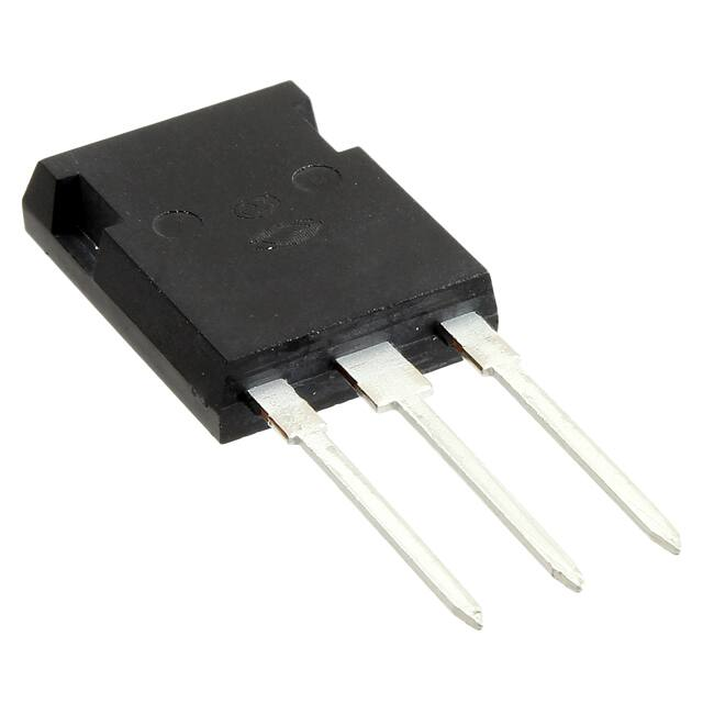
Package Outline Drawing
This section details the TO-247 package drawing of the MSC050SDA170B device. Dimensions are in
millimeters and (inches).
Figure 8 • Package Outline Drawing
053-4095 MSC050SDA0170B Datasheet Revision A
6
�Microsemi Headquarters
One Enterprise, Aliso Viejo,
CA 92656 USA
Within the USA: +1 (800) 713-4113
Outside the USA: +1 (949) 380-6100
Sales: +1 (949) 380-6136
Fax: +1 (949) 215-4996
Email: sales.support@microsemi.com
www.microsemi.com
© 2019 Microsemi. All rights reserved. Microsemi and the Microsemi logo
are trademarks of Microsemi Corporation. All other trademarks and service
marks are the property of their respective owners.
Microsemi makes no warranty, representation, or guarantee regarding the information contained herein or the suitability of its products and services
for any particular purpose, nor does Microsemi assume any liability whatsoever arising out of the application or use of any product or circuit. The
products sold hereunder and any other products sold by Microsemi have been subject to limited testing and should not be used in conjunction with
mission-critical equipment or applications. Any performance specifications are believed to be reliable but are not verified, and Buyer must conduct and
complete all performance and other testing of the products, alone and together with, or installed in, any end-products. Buyer shall not rely on any data
and performance specifications or parameters provided by Microsemi. It is the Buyer's responsibility to independently determine suitability of any
products and to test and verify the same. The information provided by Microsemi hereunder is provided "as is, where is" and with all faults, and the
entire risk associated with such information is entirely with the Buyer. Microsemi does not grant, explicitly or implicitly, to any party any patent rights,
licenses, or any other IP rights, whether with regard to such information itself or anything described by such information. Information provided in this
document is proprietary to Microsemi, and Microsemi reserves the right to make any changes to the information in this document or to any products
and services at any time without notice.
Microsemi, a wholly owned subsidiary of Microchip Technology Inc. (Nasdaq: MCHP), offers a comprehensive portfolio of semiconductor and system
solutions for aerospace & defense, communications, data center and industrial markets. Products include high-performance and radiation-hardened
analog mixed-signal integrated circuits, FPGAs, SoCs and ASICs; power management products; timing and synchronization devices and precise time
solutions, setting the world's standard for time; voice processing devices; RF solutions; discrete components; enterprise storage and communication
solutions; security technologies and scalable anti-tamper products; Ethernet solutions; Power-over-Ethernet ICs and midspans; as well as custom design
capabilities and services. Microsemi is headquartered in Aliso Viejo, California, and has approximately 4,800 employees globally. Learn more at www.
microsemi.com.
053-4095 | March 2019 | Preliminary
053-4095 MSC050SDA0170B Datasheet Revision A
7
�