.
MSC70SM120JCU2
Datasheet
Boost Chopper SiC MOSFET Power Module
January 2020
�Contents
Contents
Revision History....................................................................................................................................1
1.1 Revision 1.0.........................................................................................................................................................1
Product Overview.................................................................................................................................2
2.1 Features..............................................................................................................................................................3
2.2 Benefits...............................................................................................................................................................3
2.3 Applications........................................................................................................................................................3
Electrical Specifications........................................................................................................................4
3.1 SiC MOSFET Characteristics................................................................................................................................4
3.2 SiC Chopper Diode Ratings and Characteristics..................................................................................................6
3.3 Thermal and Package Characteristics.................................................................................................................6
3.4 SiC MOSFET Performance Curves.......................................................................................................................7
3.5 SiC Diode Performance Curves.........................................................................................................................10
4 Package Specifications.....................................................................................................................11
4.1 Package Outline Drawing..................................................................................................................................11
Microsemi Proprietary and Confidential MSC70SM120JCU2 Datasheet Revision 1.0
ii
�Revision History
1
Revision History
The revision history describes the changes that were implemented in the document. The changes are listed
by revision, starting with the most current publication.
1.1
Revision 1.0
Revision 1.0 was published in January 2020. It is the first publication of this document.
Microsemi Proprietary and Confidential MSC70SM120JCU2 Datasheet Revision 1.0
1
�Product Overview
2
Product Overview
The MSC70SM120JCU2 device is a 1200 V, 89 A full Silicon Carbide power module.
Figure 1 • Electrical Schematic of MSC70SM120JCU2 Device
Figure 2 • SOT-227 Pinout Location
All ratings at Tj = 25 °C, unless otherwise specified.
Caution: These devices are sensitive to electrostatic discharge. Proper handling procedures should be
followed.
Microsemi Proprietary and Confidential MSC70SM120JCU2 Datasheet Revision 1.0
2
�Product Overview
2.1
Features
The following are the features of MSC70SM120JCU2 device:
• SiC power MOSFET
◦ Low RDS(on)
◦ High temperature performance
• SiC Schottky diode
◦ Zero reverse recovery
◦ Zero forward recovery
◦ Temperature independent switching behavior
◦ Positive temperature coefficient on VF
2.2
Benefits
The following are the benefits of MSC70SM120JCU2 device:
• High efficiency converter
• Very low stray inductance
• Outstanding performance at high frequency operation
• Stable temperature behavior
• Direct mounting to heatsink (isolated package)
• Low junction-to-case thermal resistance
• RoHS compliant
2.3
Applications
The following are the applications of MSC70SM120JCU2 device:
• AC and DC motor control
• Switched mode power supplies
• Power factor correction
• Brake switch
Microsemi Proprietary and Confidential MSC70SM120JCU2 Datasheet Revision 1.0
3
�Electrical Specifications
3
Electrical Specifications
This section provides the electrical specifications for the MSC70SM120JCU2 device.
3.1
SiC MOSFET Characteristics
The following table shows the absolute maximum ratings of MSC70SM120JCU2 device.
Table 1 • Absolute Maximum Ratings
Symbol
Parameters
Maximum Ratings
Unit
VDSS
Drain–source voltage
1200
V
ID
Continuous drain current
TC = 25 °C
891
A
TC = 80 °C
711
IDM
Pulsed drain current
180
VGS
Gate–source voltage
–10/25
V
RDSon
Drain–source ON resistance
31
mΩ
PD
Power dissipation
395
W
TC = 25 °C
Note:
1. Specification of SiC MOSFET device but output current must be limited due to size of
power connectors.
The following table shows the electrical characteristics of MSC70SM120JCU2 device.
Table 2 • Electrical Characteristics
Symbol
Characteristics
Test Conditions
IDSS
Zero gate voltage drain current
RDS(on)
Drain–source on resistance
Typ
Max
Unit
VGS = 0 V ; VDS = 1200 V
10
100
μA
VGS = 20 V
TC = 25 °C
25
31
mΩ
TC = 175 °C
40
ID = 40 A
VGS(th)
Gate threshold voltage
VGS = VDS, ID = 1 mA
IGSS
Gate–source leakage current
VGS = 20 V, VDS = 0 V
Min
1.8
Microsemi Proprietary and Confidential MSC70SM120JCU2 Datasheet Revision 1.0
2.8
V
150
nA
4
�Electrical Specifications
The following table shows the dynamic characteristics of MSC70SM120JCU2 device.
Table 3 • Dynamic Characteristics
Symbol
Characteristics
Test Conditions
Ciss
Input capacitance
VGS = 0 V
Min
Typ
Max
3020
VDS = 1000 V
Unit
pF
Coss
Output capacitance
270
Crss
Reverse transfer capacitance
Qg
Total gate charge
Qgs
Gate–source charge
Qgd
Gate–drain charge
Td(on)
Turn-on delay time
Tr
Rise time
Td(off)
Turn-off delay time
Tf
Fall time
Eon
Turn on energy
Inductive Switching
Tj = 150°C
0.99
mJ
Eoff
Turn off energy
VGS = –5/20 V
Tj = 150°C
0.66
mJ
0.88
Ω
f = 1 MHz
25
VGS= –5/20 V
232
VBus = 800 V
nC
41
ID = 40 A
50
VGS = –5/20 V
30
VBus = 600 V
ns
30
ID = 50 A
RGon = 8 Ω
50
RGoff = 4.7 Ω
25
VBus = 600 V
ID = 50A
RGon = 8 Ω
RGoff = 4.7 Ω
RGint
Internal gate resistance
RthJC
Junction-to-case thermal resistance
0.38
°C/W
The following table shows the body diode ratings and characteristics of MSC70SM120JCU2 device.
Table 4 • Body Diode Ratings and Characteristics
Symbol
Characteristics
Test Conditions
VSD
Diode forward voltage
VGS = 0 V
Min
Typ
4
Max
Unit
V
ISD = 40 A
VGS = –5 V
4.2
ISD = 40 A
trr
Reverse recovery time
Qrr
Reverse recovery charge
Irr
Reverse recovery current
ISD = 40 A
VGS = –5 V
VR = 800 V
diF/dt = 1000 A/μs
90
ns
550
nC
13.5
A
Microsemi Proprietary and Confidential MSC70SM120JCU2 Datasheet Revision 1.0
5
�Electrical Specifications
3.2
SiC Chopper Diode Ratings and Characteristics
The following table shows the SiC chopper diode ratings and characteristics of MSC70SM120JCU2 device.
Table 5 • SiC Chopper Diode Ratings and Characteristics
Symbol Characteristics
VRRM
Peak repetitive reverse voltage
IRM
Reverse leakage current
IF
DC forward current
VF
Diode forward voltage
VR=1200 V
IF = 50 A
Min
Typ
TJ = 25 °C
15
TJ = 175 °C
250
TC = 100 °C
50
TJ = 25 °C
1.5
TJ = 175 °C
2.1
Max
Unit
1200
V
400
μA
A
1.8
V
QC
Total capacitive charge
VR = 600 V
224
nC
C
Total capacitance
f = 1 MHz, VR = 400 V
246
pF
f = 1 MHz, VR = 800 V
182
RthJC
3.3
Test Conditions
Junction-to-case thermal resistance
0.56
°C/W
Thermal and Package Characteristics
The following table shows the thermal and package characteristics of MSC70SM120JCU2 device.
Table 6 • Thermal and Package Characteristics
Symbol
Characteristics
Min
Typ
Max
VISOL
RMS isolation voltage, any terminal to case t =1 min, 50/60 Hz
2500
TSTG
Storage temperature range
–55
175
TJ
Operating junction temperature range
–55
175
TJOP
Recommended junction temperature under switching conditions
–55
TJmax–25
Torque
Terminals and mounting screws
Wt
Package weight
Unit
V
1.1
29.2
Microsemi Proprietary and Confidential MSC70SM120JCU2 Datasheet Revision 1.0
°C
N.m
g
6
�Electrical Specifications
3.4
SiC MOSFET Performance Curves
The following images show the SiC MOSFET performance curves of the MSC70SM120JCU2 device.
Figure 3 • Maximum Thermal Impedance
Figure 4 • Output Characteristics, TJ=25 °C
Figure 5 • Output Characteristics, TJ=175 °C
Figure 6 • Normalized RDS(on) vs. Temperature
Figure 7 • Transfer Characteristics
Microsemi Proprietary and Confidential MSC70SM120JCU2 Datasheet Revision 1.0
7
�Electrical Specifications
Figure 8 • Switching Energy vs. Rg
Figure 9 • Switching Energy vs. Current
Figure 10 • Capacitance vs. Drain Source Voltage
Figure 11 • Gate Charge vs. Gate Source Voltage
Figure 12 • Body Diode Characteristics, TJ=25 °C
Figure 13 • 3rd Quadrant Characteristics, TJ=25 °C
Microsemi Proprietary and Confidential MSC70SM120JCU2 Datasheet Revision 1.0
8
�Electrical Specifications
Figure 14 • Body Diode Characteristics, TJ=175 °C
Figure 15 • 3rd Quadrant Characteristics, TJ=175 °C
Figure 16 • Operating Frequency vs. Drain Current
Microsemi Proprietary and Confidential MSC70SM120JCU2 Datasheet Revision 1.0
9
�Electrical Specifications
3.5
SiC Diode Performance Curves
The following images show the SiC diode performance curves of MSC70SM120JCU2 device.
Figure 17 • Maximum Thermal Impedance
Figure 18 • Forward Characteristics
Figure 19 • Capacitance vs. Reverse Voltage
Microsemi Proprietary and Confidential MSC70SM120JCU2 Datasheet Revision 1.0
10
�Package Specifications
4
Package Specifications
The following section shows the package specification of MSC70SM120JCU2 device.
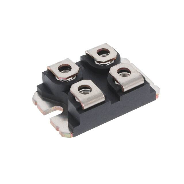
4.1
Package Outline Drawing
The following image illustrates the package outline drawing of MSC70SM120JCU2 device. The dimensions
are in millimeters and (inches).
Figure 20 • Package Outline Drawing
Microsemi Proprietary and Confidential MSC70SM120JCU2 Datasheet Revision 1.0
11
�Legal
Microsemi
2355 W. Chandler Blvd.
Chandler, AZ 85224 USA
Within the USA: +1 (480) 792-7200
Fax: +1 (480) 792-7277
www.microsemi.com © 2020 Microsemi and
its corporate affiliates. All rights reserved.
Microsemi and the Microsemi logo are
trademarks of Microsemi Corporation and its
corporate affiliates. All other trademarks and
service marks are the property of their
respective owners.
Microsemi's product warranty is set forth in Microsemi's Sales Order Terms and Conditions. Information
contained in this publication is provided for the sole purpose of designing with and using Microsemi
products. Information regarding device applications and the like is provided only for your convenience
and may be superseded by updates. Buyer shall not rely on any data and performance specifications or
parameters provided by Microsemi. It is your responsibility to ensure that your application meets with
your specifications. THIS INFORMATION IS PROVIDED "AS IS." MICROSEMI MAKES NO REPRESENTATIONS
OR WARRANTIES OF ANY KIND WHETHER EXPRESS OR IMPLIED, WRITTEN OR ORAL, STATUTORY OR
OTHERWISE, RELATED TO THE INFORMATION, INCLUDING BUT NOT LIMITED TO ITS CONDITION, QUALITY,
PERFORMANCE, NON-INFRINGEMENT, MERCHANTABILITY OR FITNESS FOR A PARTICULAR PURPOSE.
IN NO EVENT WILL MICROSEMI BE LIABLE FOR ANY INDIRECT, SPECIAL, PUNITIVE, INCIDENTAL OR
CONSEQUENTIAL LOSS, DAMAGE, COST OR EXPENSE WHATSOEVER RELATED TO THIS INFORMATION
OR ITS USE, HOWEVER CAUSED, EVEN IF MICROSEMI HAS BEEN ADVISED OF THE POSSIBILITY OR THE
DAMAGES ARE FORESEEABLE. TO THE FULLEST EXTENT ALLOWED BY LAW, MICROSEMI’S TOTAL LIABILITY
ON ALL CLAIMS IN RELATED TO THIS INFORMATION OR ITS USE WILL NOT EXCEED THE AMOUNT OF
FEES, IF ANY, YOU PAID DIRECTLY TO MICROSEMI FOR THIS INFORMATION. Use of Microsemi devices
in life support, mission-critical equipment or applications, and/or safety applications is entirely at the
buyer’s risk, and the buyer agrees to defend and indemnify Microsemi from any and all damages, claims,
suits, or expenses resulting from such use. No licenses are conveyed, implicitly or otherwise, under any
Microsemi intellectual property rights unless otherwise stated.
Microsemi Corporation, a subsidiary of Microchip Technology Inc. (Nasdaq: MCHP),
and its corporate affiliates are leading providers of smart, connected and secure
embedded control solutions. Their easy-to-use development tools and
comprehensive product portfolio enable customers to create optimal designs which
reduce risk while lowering total system cost and time to market. These solutions
serve more than 120,000 customers across the industrial, automotive, consumer,
aerospace and defense, communications and computing markets. Headquartered
in Chandler, Arizona, the company offers outstanding technical support along with
dependable delivery and quality. Learn more at www.microsemi.com.
MSCC-0344-DS-01050-1.0-0120
Microsemi Proprietary and Confidential MSC70SM120JCU2 Datasheet Revision 1.0
12
�