MTS62C19A
Dual Full-Bridge Motor Driver
Features
Description
•
•
•
•
•
•
•
•
•
The MTS62C19A motor driver is a CMOS device capable of driving both windings of a bipolar stepper motor
or bidirectionally control two DC motors. Each of the
two independent H-bridge outputs is capable of sustaining 40V and delivering up to 750 mA of continuous
current. The output current level is controlled by an
internal pulse-width modulation (PWM) circuit that is
configured using two logic inputs, a current sense
resistor, and a selectable reference voltage. The
H-bridge outputs have been optimized to provide a low
output saturation voltage drop.
•
•
•
•
750 mA Continuous Output Current
Load Voltage Supply: 10V to 40V
Full Bipolar Stepper Motor Drive Capability
Bidirectional DC Motor Capability
Internal Fixed TOFF Time PWM Current Control
Internal Protection Diodes
Internal Thermal Shutdown
Under Voltage Lockout
LS-TTL Compatible Logic Inputs with Pull-Up
Resistors
Low RON Output Resistance
Low Quiescent Current
Operating Temperature Range: -40°C to +105°C
Pin Compatible with Allegro 6219
Applications
•
•
•
•
Stepper Motor Actuators
DC Motor Actuators
Automotive HVAC Ventilation
Automotive Power Seats
Note:
The MTS62C19A device is formerly a
product of Advanced Silicon.
Full, half and micro-stepping operations are possible
with the PWM current control and logic inputs. The
maximum output current is set by a sensing resistor
and a user-selectable reference voltage. The output
current limit is selected using two logic level inputs. The
selectable output current limits are 0%, 33%, 67% or
100% of the maximum output current. Each bridge has
a PHASE input signal which is used to control the
direction of current flow through the H-bridge and the
load.
The H-bridge power stage is controlled by non-overlapping signals which prevent current cross conduction
when switching the direction of the current flow. Internal
clamp diodes protect against inductive transients.
Thermal protection circuitry disables the outputs when
the junction temperature exceeds the safe operating
limit. No special power-up sequencing is required.
Undervoltage Lockout circuitry prevents the chip from
operating when the load supply is applied prior to the
logic supply.
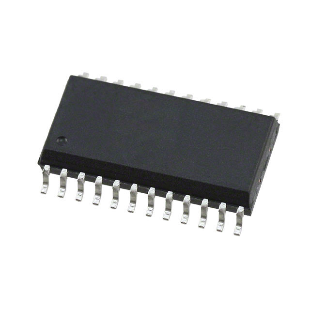
The device is supplied in a 24-pin SOP Package.
Package Types
MTS62C19A
SOP-24
OUT1A
1
24
VLOAD
OUT2A
SENSE2
COMPIN2
OUT2B
GND
GND
I02
2
3
4
5
23
22
21
20
SENSE1
COMPIN1
OUT1B
I01
6
7
8
19
18
17
GND
GND
I11
9
16
PHASE1
PHASE2
10
15
VREF1
VREF2
11
14
RC1
RC2
12
13
VLOGIC
I12
2010-2013 Microchip Technology Inc.
DS22260C-page 1
�MTS62C19A
Functional Block Diagram
VLOGIC
VLOAD
PHASE1
I01
Drivers
Shift
Logic
OUT1A
Power
Bridge
I11
Current
Sense
Comparator
VREF1
OUT1B
One-shot
Thermal
Shutdown
Under-V
Lockout
PHASE2
Shift
Logic
I02
Drivers
Power
Bridge
I12
Current
Sense
Comparator
VREF2
COMPIN1
DS22260C-page 2
COMPIN2
OUT2A
OUT2B
One-shot
RC2
RC1
GND
SENSE1
SENSE2
2010-2013 Microchip Technology Inc.
�MTS62C19A
Typical Application
5V
10 to 30V
100 µF
100 nF
VLOGIC
100 nF
VLOAD
PHASE1
I01
I11
Shift
Logic
Drivers
Power
Bridge
OUT1A
OUT1B
Logic/µP
VREF1
Current
Sense
Comparator
One-shot
Under-V
Lockout
PHASE2
I02
Shift
Drivers
OUT2A
Logic
I12
VREF2
Thermal
Shutdown
Power
Bridge
Current
Sense
Comparator
M
One-shot
RC2
COMPIN1 COMPIN2
RC1
Ct
Rt
2010-2013 Microchip Technology Inc.
OUT2B
Ct
CC
RC
CC
RC
GND
Rt
SENSE2
SENSE1
RS
RS
DS22260C-page 3
�MTS62C19A
1.0
ELECTRICAL
CHARACTERISTICS
† Notice: Stresses above those listed under “Maximum
Ratings” may cause permanent damage to the device.
This is a stress rating only and functional operation of
the device at those or any other conditions above those
indicated in the operational listings of this specification
is not implied. Exposure to maximum rating conditions
for extended periods may affect device reliability.
Absolute Maximum Ratings †
Logic Supply Voltage (VLOGIC) ......................... -0.3 to +5.5V
Load Supply Voltage (VLOAD) .......................... -0.3 to +40.0V
Logic Input Voltage Range (VIN) ....... -0.3 to VLOGIC + 0.3V
VREF Voltage Range (VREF) ............................. -0.3 to +10.0V
Output Current (Peak) ..................................................... ±1A
Output Current (Continuous) ...................................... ±0.75A
Sense Output Voltage ...................................... -0.3V to 1.5V
Junction Temperature (TJ).............................-40°C to +150°C
Operating Temperature Range (TOPR)..........-40°C to +105°C
Storage Temperature Range (TSTG) .............-55°C to +150°C
ELECTRICAL CHARACTERISTICS
Electrical Specifications: Unless otherwise specified, all limits are established for VLOGIC = 4.5V to 5.5V,
VLOAD = 30V,VREF = 5V, TA = +25°C
Parameters
Sym
Min
Typ
Max
Units
Conditions
DC Characteristics
Logic Supply Voltage
VLOGIC
4.5
5.0
5.5
V
Load Supply Voltage
VLOAD
10
30
40
V
Logic Supply Current
IVLOGIC
—
0.8
1.0
mA
VREF Voltage Range
VREF
1.5
5.0
7.0
V
IVLOAD_ON
—
0.55
1.0
mA
Both Bridges ON, No Load
IVLOAD_OFF
—
0.55
1.0
mA
Both Bridges Off
Control Logic
Input Current (VIN = 0V)
IIN
—
—
-70
µA
I01, I11, I02, I12, PHASE1,
PHASE2, (Note 1)
Logic-Low
Input Voltage
VIL
—
—
0.8
V
I01, I11, I02, I12, PHASE1,
PHASE2
Logic-High
Input Voltage
VIH
2.4
—
—
V
I01, I11, I02, I12, PHASE1,
PHASE2
9.5
10
10.5
—
I0 = L, I1 = L
13.5
15
16.5
—
I0 = H, I1 = L
Driver Supply Current
Current Limit Threshold
Ratio (VREF ÷ VSENSE)
Driver Output Saturation Voltage VCE(SAT)
Clamp Diode Forward
Voltage (Note 2)
Driver Output
Leakage Current
Thermal Shutdown
Temperature
VREF_VSENSE
25.5
30
34.5
—
I0 = L, I1 = H
VONN
(Low Side)
—
0.55
0.65
V
(Sink) IOUT = +500 mA
—
0.90
1.00
V
(Sink) IOUT = +750 mA
VONP
(High Side)
—
1.05
1.40
V
(Source) IOUT = -500 mA
—
1.85
2.10
V
(Source) IOUT = -750 mA
VF_NDIODE
—
0.95
1.30
V
IF = 750 mA
VF_PDIODE
—
1.00
1.30
V
IF = 750 mA
ILEAK
—
—
-50
µA
VOUT = 0V
—
—
50
µA
VOUT = VLOAD
TJ_SHDN
—
170
—
°C
TOFF
—
50
58
µs
TD
—
1.5
10
µs
AC Characteristics
Cut-off Time
(one-shot pulse)
Turn-off Delay
Note 1:
2:
Rs = 1, RC = 1 k, CC = 820 pF,
Rt = 56 k, Ct = 820 pF
VIN = 5.0V input current given by internal pull-up to Logic Supply.
Clamp/Freewheel diode is the intrinsic body-drain diode of the NMOS and PMOS transistors.
DS22260C-page 4
2010-2013 Microchip Technology Inc.
�MTS62C19A
TEMPERATURE SPECIFICATIONS
Parameters
Sym
Min
Junction Temperature Range
TJ
Operating Temperature Range
Typ
Max
Units
Conditions
-40
+125
°C
TA
-40
+105
°C
Thermal Resistance, SOP-24
JA
—
76
—
°C/W EIA/JEDEC JESD51-10
Thermal Resistance, SOP-24
JC
—
16
—
°C/W EIA/JEDEC JESD51-10
Recommended Temperature Ranges
Thermal Package Resistance
2010-2013 Microchip Technology Inc.
DS22260C-page 5
�MTS62C19A
2.0
PIN DESCRIPTIONS
The descriptions of the pins are listed in Table 2-1.
TABLE 2-1:
MTS62C19A PIN FUNCTION TABLE
Pin No.
SOP-24
Type
Name
1
Output
OUT1A
Output 1 ‘A’ Side of Motor Winding
2
Output
OUT2A
Output 2 ‘A’ Side of Motor Winding
3
Input
SENSE2
Current Sense for Output 2
4
Input
COMPIN2
Current Sense Comparator Input for Output 2
5
Output
OUT2B
6
Power
GND
7
Power
GND
Negative Logic Supply (Ground)
8
Input
I02
Output 2 Current Selection Bit 0
Output 2 Current Selection Bit 1
9
Input
I12
10
Input
PHASE2
Function
Output 2 ‘B’ Side of Motor Winding
Negative Logic Supply (Ground)
Output 2 Phase
11
Input
VREF2
Output 2 Current Reference
12
Input
RC2
Output 2 RC Time Constant
13
Power
VLOGIC
14
Input
RC1
Output 1 RC Time Constant
15
Input
VREF1
Output 1 Current Reference
16
Input
PHASE1
Positive Logic Supply Voltage
Output 1 Phase
17
Input
I11
Output 1 Current Selection Bit 1
18
Power
GND
Negative Logic Supply (Ground)
19
Power
GND
Negative Logic Supply (Ground)
20
Input
I01
Output 1 Current Selection Bit 0
21
Output
OUT1B
22
Input
COMPIN1
23
Input
SENSE1
24
Power
VLOAD
DS22260C-page 6
Output 1 ‘B’ Side of Motor Winding
Current Sense Comparator Input for Output 1
Current Sense for Output 1
Positive Load Supply Voltage
2010-2013 Microchip Technology Inc.
�MTS62C19A
2.1
Output Stage (OUT1A, OUT2A,
OUT1B, OUT2B)
Output connection to “A” side and “B” side of motor
windings.
2.2
Current Sense Input (SENSE1,
SENSE2)
2.6
Current Flow Direction Selection
(PHASE1, PHASE2)
Logic input to select the direction of the current flow
through the load. A “HIGH” logic signal level causes
load current to flow from OUTxA to OUTxB. A “LOW”
logic level causes load current to flow from OUTxB to
OUTxA.
Connection to lower sources of output stage for
insertion of current sense resistor.
2.7
2.3
Reference voltage for current sense comparator.
Determines the level of output current detection
together with sensing resistor and inputs I0x, I1x.
Current Sense Comparator Input
(COMPIN1, COMPIN2)
Current Sense Reference
(VREF1, VREF2)
Current sense comparator input.
2.8
2.4
Ground Terminal (GND)
Logic supply ground. Only the driver current flows out
of this pin; there is no high current. Minimize voltage
drops between this pin and the logic inputs.
2.5
Current Detection Selection
(I01, I02, I11, I12)
Comparator input for current threshold detection. The
voltage across the sense resistor is fed back to this
input through the low-pass filter RcCc. The power transistors are disabled when the sense voltage exceeds
the reference voltage of the selected comparator.
When this occurs, the current decays for a time set by
RtCt (TOFF = 1.1 RtCt).
2010-2013 Microchip Technology Inc.
Output Stage OFF Time
(RC1, RC2)
A parallel RtCt network connected to this pin sets the
OFF time of the power transistors. The monostable
pulse generator is triggered by the output of the current
sense comparator.
2.9
Logic Supply Voltage (VLOGIC)
Connect VLOGIC to the logic source voltage. Decouple
the supply with a 0.1 µF ceramic capacitor mounted
close to the VLOGIC and GND terminals.
2.10
Load Supply Voltage (VLOAD)
Connect VLOAD to the motor positive voltage supply.
The motor current is supplied through this pin and the
selected output transistors.
DS22260C-page 7
�MTS62C19A
3.0
FUNCTIONAL DESCRIPTION
3.1
Each motor winding is driven by an H-type bridge
consisting of two N and two P transistors that allow the
current to flow in both winding directions depending on
the value of the PHASE signal (Table 3-1). The
H-bridge can be set in five configurations that are
related to the digital inputs PHASE, I0 and I1 and to the
current sensed. These configurations are shown in
Table 3-2.
The circuit is designed to drive the two windings of a
bipolar stepper motor, and can be divided in two identical channels (channel 1 and channel 2) and protection
circuitry for overtemperature and undervoltage. The
functionality of a channel and protection circuitry is
presented in the following sections.
VLOAD
Power Bridge Operation
VLOAD
VLOAD
Pb
Pa
H
L
L
L
H
Na
Nb
L
H
Na
Nb
SENSE
RS
OUTB
OUTA
H
Na
H
L
OUTB
OUTA
Pb
Pa
H
L
OUTB
OUTA
Pb
Pa
Nb
SENSE
SENSE
RS
a)
RS
c)
b)
Legend: a) Bridge ON, b) Source OFF, c) All OFF/Coasting
Note: For PHASE = L/Reverse, invert A and B in drawings.
FIGURE 3-1:
Power Bridge Control (PHASE = H/forward).
TABLE 3-1:
CURRENT DIRECTION CONTROL
Phase
Output Current
L
Current flows from OUTxB to OUTxA
H
Current flows from OUTxA to OUTxB
TABLE 3-2:
POWER BRIDGE GATE CONTROL TRUTH TABLE
I0I1
PHASE
Overi
TOFF
Case/Mode
gna
gpa
gnb
gpb
00/01/10
1
0
0
Forward ON
L
00/01/10
1
x
1
Forward OFF
L
L
H
H
H
H
H
00/01/10
0
0
0
Reverse ON
H
H
L
L
00/01/10
0
x
1
Reverse OFF
H
H
L
H
11
x
x
x
No Current/
Coasting
L
H
L
H
Legend: Bold = Active MOS Transistors, Overi = Overcurrent flag, TOFF = Channel TOFF State Flag
DS22260C-page 8
2010-2013 Microchip Technology Inc.
�MTS62C19A
3.2
PWM Current Control
The current level in each motor winding is controlled by
a PWM circuit with a fixed TOFF time. The load current
flowing in the winding is sensed through an external
sensing resistor RS, connected between the power
bridge's source pin SENSE (sources of transistors Na
and Nb) and GND.
VLOAD
Power
Bridge
VREF
Pa
Pb
One-Shot
OUTA
÷10
Source
Disable
OUTB
I0
I1
FIGURE 3-2:
Na
COMPIN
CC
RC
RC
Ct
SENSE
RS
Rt
PWM Current Control Circuit Principle (Channel 1 Shown).
The voltage across RS is compared to a fraction of the
reference voltage VREF, chosen with the logic input bits
I0 and I1 (Table 3-3). The power bridge, and thus the
load current, can also be switched off completely when
both logic inputs are high. Note that any logic input left
unconnected will be treated as a high level (pull-up
resistor).
TABLE 3-3:
Nb
The maximum trip current for regulation, given for
I0 I1 = 00 is calculated in Equation 3-1.
EQUATION 3-1:
V REF
I MAX = -----------------10 R S
CURRENT LEVEL CONTROL TRUTH TABLE
I0
I1
Comp. Trip Voltage
Output Current
0
0
VTRIP = 1/10 x VREF
IMAX = VREF/10RS
1
0
VTRIP = 1/15 x VREF
2/3 x IMAX = VREF/15RS
0
1
VTRIP = 1/30 x VREF
1/3 x IMAX = VREF/30RS
1
1
x
0 (no current)
2010-2013 Microchip Technology Inc.
DS22260C-page 9
�MTS62C19A
When the maximum allowed current is reached, the
bridge source is turned off during a fixed period TOFF
(typically 50 µs) given by a non-retriggerable pulse
generator and the external timing components Rt
(20k – 100 k range) and Ct (100 pF – 1000 pF
range):
EQUATION 3-2:
3.3
A thermal protection circuitry turns off all drivers when
the junction temperature exceeds a safe operating limit
of +170°C (typical). This protects the devices from
failure due to excessive heating. Despite this thermal
protection, output short circuits are not permitted. The
output drivers are re-enabled once junction
temperature has dropped below +145°C (typical).
T OFF = 1.1 R t C t
During TOFF the winding current decreases. When the
driver is re-enabled, the winding current increases
again until it reaches the threshold, and the cycle
repeats itself, maintaining the load current at the
desired level.
Circuit Protection
thshtd_en
1
PHASE
0
IOUT +0
+145°C
+170°C
-
IOUT
t
ton d
FIGURE 3-3:
Waveform.
DS22260C-page 10
toff
PWM Output Current
FIGURE 3-4:
Thermal Shutdown Output
vs. Temperature Showing Hysteresis.
An undervoltage lockout circuit protects the
MTS62C19A from potential shoot-through currents
when the load supply voltage is applied prior to the
logic supply voltage. The power bridge and all outputs
are disabled if VLOGIC is smaller than 4V.
With this protection feature, the circuit will withstand
any order of turn-on or turn-off of the supply voltages
VLOGIC and VLOAD. Normal dV/dt values are assumed.
2010-2013 Microchip Technology Inc.
�MTS62C19A
4.0
APPLICATION CIRCUITS AND
ISSUES
4.1
Typical Application
The MTS62C19A circuit, with external components for
a typical application, is shown in Figure 4-1. Typical
passive component values are: RS = 1, RC = 1 k,
CC = 820 pF, Rt = 56 k and Ct = 820 pF.
5V
10 to 30V
100 µF
100 nF
VLOGIC
100 nF
VLOAD
PHASE1
I01
I11
Shift
Logic
Drivers
Power
Bridge
OUT1A
OUT1B
Logic/µP
VREF1
Current
Sense
Comparator
One-shot
Under-V
Lockout
PHASE2
I02
Shift
OUT2A
Power
Bridge
Current
Sense
Comparator
OUT2B
M
One-shot
RC2
COMPIN1 COMPIN2
RC1
Ct
Rt
FIGURE 4-1:
Drivers
Logic
I12
VREF2
Thermal
Shutdown
Ct
CC
RC
CC
RC
GND
Rt
SENSE2
SENSE1
RS
RS
Typical Application Circuit.
During PWM operation, when the output stage is
turned-on, large voltage peaks might appear across
RS, which can wrongly trigger the input comparator. To
avoid an unstable current control, an external RCCC filter should be used that delays the comparator action.
Depending on load type, many applications will not
require this filter (SENSE connected to COMPIN).
2010-2013 Microchip Technology Inc.
DS22260C-page 11
�MTS62C19A
4.2
Stepping Examples
The MTS62C19A control modes are full-step, halfstep, modified half-step and microstepping control of
the motor, as shown in Figure 4-2.
Half-Step
Full-Step
1
2
3
4
1 2 3 4 5 6 7 8
Modified Half-Step
1 2 3 4 5 6 7 8
Micro-Stepping (1/8th)
1...
...32
I01
I11
PHASE1
I02
I12
PHASE2
5V
VREF1
VREF2
0V
5V
5V
5V
5V
0V
+500 mA
Motor Current
in Phase 1
0
-500 mA
+167 mA
Motor Current
in Phase 2
FIGURE 4-2:
4.3
-167 mA
+500 mA
+333 mA
0
-333 mA
-500 mA
Examples of Stepping Modes Achievable with Typical Application Circuit.
PCB Design Guidelines
Unused inputs should be connected to fixed voltage
levels in order to get the highest noise immunity. Typical PCB layout guidelines for power applications
should be followed. These include separate power
ground planes, supply decoupling capacitors close to
the IC, short connections and use of maximized copper
areas to improve thermal dissipation.
DS22260C-page 12
2010-2013 Microchip Technology Inc.
�MTS62C19A
5.0
PACKAGING INFORMATION
5.1
Package Marking Information
24-Lead SOP
Example
YYWWNNN
Legend: XX...X
Y
YY
WW
NNN
e3
*
Note:
MTS62C19A
e3
HS105 ^^
1248256
Customer-specific information
Year code (last digit of calendar year)
Year code (last 2 digits of calendar year)
Week code (week of January 1 is week ‘01’)
Alphanumeric traceability code
Pb-free JEDEC designator for Matte Tin (Sn)
This package is Pb-free. The Pb-free JEDEC designator ( e3 )
can be found on the outer packaging for this package.
In the event the full Microchip part number cannot be marked on one line, it will
be carried over to the next line, thus limiting the number of available
characters for customer-specific information.
2010-2013 Microchip Technology Inc.
DS22260C-page 13
�MTS62C19A
SOP 24L Package Outline
Note:
For the most current package drawings, please see the Microchip Packaging Specification located
at http://www.microchip.com/packaging
24
13
1
0.016 typ
12
0.05 typ
D
L
GAUGE PLANE
SEATING PLANE
Note:
The package drawing dimensions are expressed in inches.
Symbol
Minimum
Typical
A
—
—
Note 1:
2:
3:
A1
0.102 (0.004)
D
15.545 (0.612)
Maximum
2.642 (0.104)
—
15.697 (0.618)
—
Unit
mm (inch)
mm (inch)
15.850 (0.624)
mm (inch)
E
7.417 (0.292)
7.518 (0.296)
7.595 (0.299)
mm (inch)
H
10.287 (0.405)
10.464 (0.412)
10.643 (0.419)
mm (inch)
L
0.533 (0.021)
0.787 (0.031)
1.041 (0.041)
mm (inch)
J
0
4
8
°
JEDEC outline: M0-119 AA
Dimensions “D” does not include mold flash, protrusions or gate burrs. Mold flash, protrusions
and gate burrs should not exceed 0.25mm (0.010inch) per side.
Dimensions “E” does not include inter-lead flash, or protrusions. Inter-lead flash and protrusions
shall not exceed 0.25mm (0.010 inch) per side.
DS22260C-page 14
2010-2013 Microchip Technology Inc.
�MTS62C19A
APPENDIX A:
REVISION HISTORY
Revision C (March 2013)
The following is the list of modifications:
1.
2.
Corrected one dimension in the package
drawing. Added a note mentioning the unit type
used in the drawing.
Minor editorial changes.
Revision B (December 2012)
The following is the list of modifications:
1.
2.
3.
4.
Updated Operating Temperature Range
throughout the document.
Corrected Typical Application diagram.
Added
Section 5.1,
Package
Marking
Information.
Added Product Identification System section.
Revision A (September 2010)
• Original Release of this Document.
2010-2013 Microchip Technology Inc.
DS22260C-page 15
�MTS62C19A
NOTES:
DS22260C-page 16
2010-2013 Microchip Technology Inc.
�MTS62C19A
PRODUCT IDENTIFICATION SYSTEM
To order or obtain information, e.g., on pricing or delivery, refer to the factory or the listed sales office.
PART NO.
-X
X
XXX
Device
Tube/Tape
and Reel
Package
Fixed
Characters
Device:
MTS62C19A: Dual Full-Bridge Motor Driver
Packing Type:
H
L
=
=
Tube
Tape and Reel
Package:
S*
=
24-Lead Plastic Small Outline (SOP)
Examples:
a)
MTS62C19A-HS105
b)
MTS62C19A-LS105
Tube,
24LD SOP Package
Tape and Reel,
24LD SOP Package
* These devices are formerly products of Advanced Silicon
2010-2013 Microchip Technology Inc.
DS22260C-page 17
�MTS62C19A
NOTES:
DS22260C-page 18
2010-2013 Microchip Technology Inc.
�Note the following details of the code protection feature on Microchip devices:
•
Microchip products meet the specification contained in their particular Microchip Data Sheet.
•
Microchip believes that its family of products is one of the most secure families of its kind on the market today, when used in the
intended manner and under normal conditions.
•
There are dishonest and possibly illegal methods used to breach the code protection feature. All of these methods, to our
knowledge, require using the Microchip products in a manner outside the operating specifications contained in Microchip’s Data
Sheets. Most likely, the person doing so is engaged in theft of intellectual property.
•
Microchip is willing to work with the customer who is concerned about the integrity of their code.
•
Neither Microchip nor any other semiconductor manufacturer can guarantee the security of their code. Code protection does not
mean that we are guaranteeing the product as “unbreakable.”
Code protection is constantly evolving. We at Microchip are committed to continuously improving the code protection features of our
products. Attempts to break Microchip’s code protection feature may be a violation of the Digital Millennium Copyright Act. If such acts
allow unauthorized access to your software or other copyrighted work, you may have a right to sue for relief under that Act.
Information contained in this publication regarding device
applications and the like is provided only for your convenience
and may be superseded by updates. It is your responsibility to
ensure that your application meets with your specifications.
MICROCHIP MAKES NO REPRESENTATIONS OR
WARRANTIES OF ANY KIND WHETHER EXPRESS OR
IMPLIED, WRITTEN OR ORAL, STATUTORY OR
OTHERWISE, RELATED TO THE INFORMATION,
INCLUDING BUT NOT LIMITED TO ITS CONDITION,
QUALITY, PERFORMANCE, MERCHANTABILITY OR
FITNESS FOR PURPOSE. Microchip disclaims all liability
arising from this information and its use. Use of Microchip
devices in life support and/or safety applications is entirely at
the buyer’s risk, and the buyer agrees to defend, indemnify and
hold harmless Microchip from any and all damages, claims,
suits, or expenses resulting from such use. No licenses are
conveyed, implicitly or otherwise, under any Microchip
intellectual property rights.
Trademarks
The Microchip name and logo, the Microchip logo, dsPIC,
FlashFlex, KEELOQ, KEELOQ logo, MPLAB, PIC, PICmicro,
PICSTART, PIC32 logo, rfPIC, SST, SST Logo, SuperFlash
and UNI/O are registered trademarks of Microchip Technology
Incorporated in the U.S.A. and other countries.
FilterLab, Hampshire, HI-TECH C, Linear Active Thermistor,
MTP, SEEVAL and The Embedded Control Solutions
Company are registered trademarks of Microchip Technology
Incorporated in the U.S.A.
Silicon Storage Technology is a registered trademark of
Microchip Technology Inc. in other countries.
Analog-for-the-Digital Age, Application Maestro, BodyCom,
chipKIT, chipKIT logo, CodeGuard, dsPICDEM,
dsPICDEM.net, dsPICworks, dsSPEAK, ECAN,
ECONOMONITOR, FanSense, HI-TIDE, In-Circuit Serial
Programming, ICSP, Mindi, MiWi, MPASM, MPF, MPLAB
Certified logo, MPLIB, MPLINK, mTouch, Omniscient Code
Generation, PICC, PICC-18, PICDEM, PICDEM.net, PICkit,
PICtail, REAL ICE, rfLAB, Select Mode, SQI, Serial Quad I/O,
Total Endurance, TSHARC, UniWinDriver, WiperLock, ZENA
and Z-Scale are trademarks of Microchip Technology
Incorporated in the U.S.A. and other countries.
SQTP is a service mark of Microchip Technology Incorporated
in the U.S.A.
GestIC and ULPP are registered trademarks of Microchip
Technology Germany II GmbH & Co. & KG, a subsidiary of
Microchip Technology Inc., in other countries.
All other trademarks mentioned herein are property of their
respective companies.
© 2010-2013, Microchip Technology Incorporated, Printed in
the U.S.A., All Rights Reserved.
Printed on recycled paper.
ISBN: 978-1-62077-053-5
QUALITY MANAGEMENT SYSTEM
CERTIFIED BY DNV
== ISO/TS 16949 ==
2010-2013 Microchip Technology Inc.
Microchip received ISO/TS-16949:2009 certification for its worldwide
headquarters, design and wafer fabrication facilities in Chandler and
Tempe, Arizona; Gresham, Oregon and design centers in California
and India. The Company’s quality system processes and procedures
are for its PIC® MCUs and dsPIC® DSCs, KEELOQ® code hopping
devices, Serial EEPROMs, microperipherals, nonvolatile memory and
analog products. In addition, Microchip’s quality system for the design
and manufacture of development systems is ISO 9001:2000 certified.
DS22260C-page 19
�Worldwide Sales and Service
AMERICAS
ASIA/PACIFIC
ASIA/PACIFIC
EUROPE
Corporate Office
2355 West Chandler Blvd.
Chandler, AZ 85224-6199
Tel: 480-792-7200
Fax: 480-792-7277
Technical Support:
http://www.microchip.com/
support
Web Address:
www.microchip.com
Asia Pacific Office
Suites 3707-14, 37th Floor
Tower 6, The Gateway
Harbour City, Kowloon
Hong Kong
Tel: 852-2401-1200
Fax: 852-2401-3431
India - Bangalore
Tel: 91-80-3090-4444
Fax: 91-80-3090-4123
India - New Delhi
Tel: 91-11-4160-8631
Fax: 91-11-4160-8632
Austria - Wels
Tel: 43-7242-2244-39
Fax: 43-7242-2244-393
Denmark - Copenhagen
Tel: 45-4450-2828
Fax: 45-4485-2829
India - Pune
Tel: 91-20-2566-1512
Fax: 91-20-2566-1513
France - Paris
Tel: 33-1-69-53-63-20
Fax: 33-1-69-30-90-79
Japan - Osaka
Tel: 81-6-6152-7160
Fax: 81-6-6152-9310
Germany - Munich
Tel: 49-89-627-144-0
Fax: 49-89-627-144-44
Atlanta
Duluth, GA
Tel: 678-957-9614
Fax: 678-957-1455
Boston
Westborough, MA
Tel: 774-760-0087
Fax: 774-760-0088
Chicago
Itasca, IL
Tel: 630-285-0071
Fax: 630-285-0075
Cleveland
Independence, OH
Tel: 216-447-0464
Fax: 216-447-0643
Dallas
Addison, TX
Tel: 972-818-7423
Fax: 972-818-2924
Detroit
Farmington Hills, MI
Tel: 248-538-2250
Fax: 248-538-2260
Indianapolis
Noblesville, IN
Tel: 317-773-8323
Fax: 317-773-5453
Los Angeles
Mission Viejo, CA
Tel: 949-462-9523
Fax: 949-462-9608
Santa Clara
Santa Clara, CA
Tel: 408-961-6444
Fax: 408-961-6445
Toronto
Mississauga, Ontario,
Canada
Tel: 905-673-0699
Fax: 905-673-6509
Australia - Sydney
Tel: 61-2-9868-6733
Fax: 61-2-9868-6755
China - Beijing
Tel: 86-10-8569-7000
Fax: 86-10-8528-2104
China - Chengdu
Tel: 86-28-8665-5511
Fax: 86-28-8665-7889
China - Chongqing
Tel: 86-23-8980-9588
Fax: 86-23-8980-9500
Netherlands - Drunen
Tel: 31-416-690399
Fax: 31-416-690340
Korea - Daegu
Tel: 82-53-744-4301
Fax: 82-53-744-4302
Spain - Madrid
Tel: 34-91-708-08-90
Fax: 34-91-708-08-91
China - Hangzhou
Tel: 86-571-2819-3187
Fax: 86-571-2819-3189
Korea - Seoul
Tel: 82-2-554-7200
Fax: 82-2-558-5932 or
82-2-558-5934
China - Hong Kong SAR
Tel: 852-2943-5100
Fax: 852-2401-3431
Malaysia - Kuala Lumpur
Tel: 60-3-6201-9857
Fax: 60-3-6201-9859
China - Nanjing
Tel: 86-25-8473-2460
Fax: 86-25-8473-2470
Malaysia - Penang
Tel: 60-4-227-8870
Fax: 60-4-227-4068
China - Qingdao
Tel: 86-532-8502-7355
Fax: 86-532-8502-7205
Philippines - Manila
Tel: 63-2-634-9065
Fax: 63-2-634-9069
China - Shanghai
Tel: 86-21-5407-5533
Fax: 86-21-5407-5066
Singapore
Tel: 65-6334-8870
Fax: 65-6334-8850
China - Shenyang
Tel: 86-24-2334-2829
Fax: 86-24-2334-2393
Taiwan - Hsin Chu
Tel: 886-3-5778-366
Fax: 886-3-5770-955
China - Shenzhen
Tel: 86-755-8864-2200
Fax: 86-755-8203-1760
Taiwan - Kaohsiung
Tel: 886-7-213-7828
Fax: 886-7-330-9305
China - Wuhan
Tel: 86-27-5980-5300
Fax: 86-27-5980-5118
Taiwan - Taipei
Tel: 886-2-2508-8600
Fax: 886-2-2508-0102
China - Xian
Tel: 86-29-8833-7252
Fax: 86-29-8833-7256
Thailand - Bangkok
Tel: 66-2-694-1351
Fax: 66-2-694-1350
UK - Wokingham
Tel: 44-118-921-5869
Fax: 44-118-921-5820
China - Xiamen
Tel: 86-592-2388138
Fax: 86-592-2388130
China - Zhuhai
Tel: 86-756-3210040
Fax: 86-756-3210049
DS22260C-page 20
Italy - Milan
Tel: 39-0331-742611
Fax: 39-0331-466781
Japan - Tokyo
Tel: 81-3-6880- 3770
Fax: 81-3-6880-3771
11/29/12
2010-2013 Microchip Technology Inc.
�