PIC16(L)F1713/6
Cost Effective 8-Bit Intelligent Analog Flash Microcontrollers
Description:
PIC16(L)F1713/6 microcontrollers combine Intelligent Analog integration with low cost and extreme low power (XLP) to
suit a variety of general purpose applications. These 28-pin devices deliver on-chip op amps, Core Independent Peripherals (CLC, NCO and COG), Peripheral Pin Select and Zero-Cross Detect, providing for increased design flexibility.
Core Features:
Digital Peripherals:
• C Compiler Optimized RISC Architecture
• Only 49 Instructions
• Operating Speed:
- 0-32 MHz clock input
- 125 ns minimum instruction cycle
• Interrupt Capability
• 16-Level Deep Hardware Stack
• Up to Four 8-bit Timers
• One 16-bit Timer
• Power-on Reset (POR)
• Power-up Timer (PWRT)
• Low-Power Brown-out Reset (LPBOR)
• Programmable Watchdog Timer (WDT) up to
256s
• Programmable Code Protection
• Configurable Logic Cell (CLC):
- Integrated combinational and sequential logic
• Complementary Output Generator (COG):
- Rising/falling edge dead-band control/
blanking
• Numerically Controlled Oscillator (NCO):
- Generates true linear frequency control and
increased frequency resolution
- Input Clock: 0Hz < FNCO < 32 MHz
- Resolution: FNCO/220
• Capture/Compare/PWM (CCP) module
• PWM: Two 10-bit Pulse-Width Modulators
• Serial Communications:
- SPI, I2C, RS-232, RS-485, LIN compatible
- Auto-Baud Detect, auto-wake-up on start
• Up to 35 I/O Pins and One Input Pin:
- Individually programmable pull-ups
- Slew rate control
- Interrupt-on-change with edge-select
• Peripheral Pin Select (PPS):
- Enables pin mapping of digital I/O
Memory:
•
•
•
•
Up to 8 Kwords Flash Program Memory
Up to 1024 Bytes Data SRAM Memory
Direct, Indirect and Relative Addressing modes
High-Endurance Flash Data Memory (HEF)
- 128 bytes if nonvolatile data storage
- 100k erase/write cycles
Operating Characteristics:
• Operating Voltage Range:
- 1.8V to 3.6V (PIC16LF1713/6)
- 2.3V to 5.5V (PIC16F1713/6)
• Temperature Range:
- Industrial: -40°C to 85°C
- Extended: -40°C to 125°C
eXtreme Low-Power (XLP) Features:
•
•
•
•
Sleep mode: 50 nA @ 1.8V, typical
Watchdog Timer: 500 nA @ 1.8V, typical
Secondary Oscillator: 500 nA @ 32 kHz
Operating Current:
- 8 uA @ 32 kHz, 1.8V, typical
- 32 uA/MHz @ 1.8V, typical
2013-2018 Microchip Technology Inc.
Intelligent Analog Peripherals:
• Operational Amplifiers:
- Two configurable rail-to-rail op amps
- Selectable internal and external channels
- 2 MHz gain bandwidth product
• High-Speed Comparators:
- Up to two comparators
- 50 ns response time
- Rail-to-rail inputs
• 10-Bit Analog-to-Digital Converter (ADC):
- Up to 28 external channels
- Conversion available during Sleep
- Temperature indicator
• Zero-Cross Detector (ZCD):
- Detect when AC signal on pin crosses
ground
• 8-Bit Digital-to-Analog Converter (DAC):
- Output available externally
- Internal connections to comparators, op
amps, Fixed Voltage Reference (FVR) and
ADC
• Internal Voltage Reference module
DS40001726D-page 1
�PIC16(L)F1713/6
Clocking Structure:
Programming/Debug Features:
• 16 MHz Internal Oscillator Block:
- ±1% at calibration
- Selectable frequency range from 0 to 32 MHz
• 31 kHz Low-Power Internal Oscillator
• External Oscillator Block with:
- Three crystal/resonator modes up to 20 MHz
- Two external clock modes up to 20 MHz
• Fail-Safe Clock Monitor
• Two-Speed Oscillator Start-up
• Oscillator Start-up Timer (OST)
• In-Circuit Debug Integrated On-Chip
• Emulation Header for Advanced Debug:
- Provides trace, background debug and up to
32 hardware break points
• In-Circuit Serial Programming™ (ICSP™) via Two
Pins
XLP
Debug(1)
PPS
NCO
CLC
MSSP (I2C/SPI)
EUSART
COG
PWM
CCP
Timers
(8/16-bit)
Zero Cross
Op Amp
High-Speed/
Comparators
5/8-bit DAC
10-bit ADC (ch)
I/Os(2)
High-Endurance
Flash (bytes)
Data SRAM
(bytes)
Device
Program Memory
Flash (words)
Family Types
Data Sheet Index
PIC16(L)F1713/6
PIC16(L)F1713
(1)
4096
512
128
25
17
1/1
2
2
1
4/1
2
2
1
1
1
4
1
Y
I/E
Y
PIC16(L)F1716
(1)
8192
1024
128
25
17
1/1
2
2
1
4/1
2
2
1
1
1
4
1
Y
I/E
Y
PIC16(L)F1717
(2)
8192
1024
128
36
28
1/1
2
2
1
4/1
2
2
1
1
1
4
1
Y
I/E
Y
PIC16(L)F1718
(2) 16384
2048
128
25
17
1/1
2
2
1
4/1
2
2
1
1
1
4
1
Y
I/E
Y
PIC16(L)F1719
(2) 16384
2048
128
36
28
1/1
2
2
1
4/1
2
2
1
1
1
4
1
Y
I/E
Y
Note 1:
2:
Debugging Methods: (I) – Integrated on Chip; (H) – using Debug Header; E – using Emulation Header.
One pin is input-only.
Data Sheet Index: (Unshaded devices are described in this document.)
1: DS40001726
PIC16(L)F1713/6 Data Sheet, 28-Pin Flash, 8-bit Microcontrollers.
2: DS40001740
PIC16(L)F1717/8/9 Data Sheet, 28/40-Pin Flash, 8-bit Microcontrollers.
Note:
For other small form-factor package availability and marking information, please visit
http://www.microchip.com/packaging or contact your local sales office.
DS40001726D-page 2
2013-2018 Microchip Technology Inc.
�PIC16(L)F1713/6
Pin Diagrams
Note:
VPP/MCLR/RE3
1
28
RB7
RA0
2
27
RB6
RA1
3
26
RB5
RA2
4
25
RB4
RA3
5
RB3
RA4
6
24
23
22
RB1
RB0
RA5
VSS
7
RA7
9
8
RA6
10
RC0
11
RC1
21
RB2
20
VDD
19
VSS
18
RC7
12
17
RC6
RC2
13
16
RC5
RC3
14
15
RC4
See Table 1 for the pin allocation table.
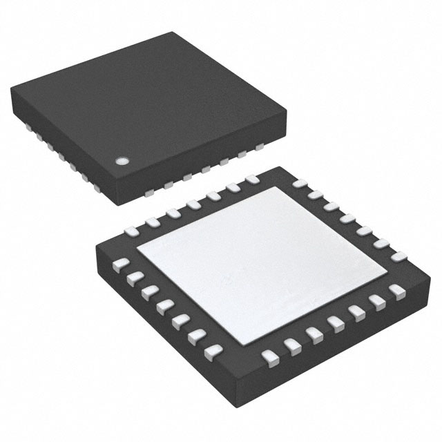
28-PIN (U)QFN
28
27
26
25
24
23
22
RA1
RA0
RE3/MCLR/VPP
RB7
RB6
RB5
RB4
FIGURE 2:
28-PIN PDIP, SOIC, SSOP
PIC16(L)F1713/6
FIGURE 1:
21
20
19
18
17
16
15
RB3
RB2
RB1
RB0
VDD
VSS
RC7
RC0
RC1
RC2
RC3
RC4
RC5
RC6
RA7
RA6
1
2
3
PIC16(L)F1713/6
4
5
6
7
8
9
10
11
12
13
14
RA2
RA3
RA4
RA5
VSS
Note:
See Table 1 for the pin allocation table.
2013-2018 Microchip Technology Inc.
DS40001726D-page 3
�C1IN0+
C2IN0+
RA3
5
2
AN3
Vref+
C1IN1+
RA4
6
3
RA5
7
4
RA6
10
RA7
CLCIN0(1)
IOC
Y
CLCIN1(1)
IOC
Y
IOC
Y
DAC1OUT1
Basic
Vref-
Pull-up
AN2
Interrupt
1
OPA1OUT
CLC
4
EUSART
RA2
MSSP
C1IN1C2IN1-
COG
AN1
PWM
28
NCO
3
CCP
RA1
Timers
C1IN0C2IN0-
Zero Cross
AN0
DAC
ADC
27
Op Amp
QFN, UQFN
2
Reference
PDIP, SOIC,
SSOP
RA0
(2)
I/O
Comparator
28-PIN ALLOCATION TABLE (PIC16(L)F1713/6)
IOC
Y
IOC
Y
IOC
Y
7
IOC
Y
OSC2
CLKOUT
9
6
IOC
Y
OSC1
CLKIN
RB0
21
18
AN12
C2IN1+
INT(1)
IOC
Y
RB1
22
19
AN10
C1IN3C2IN3-
OPA2OUT
IOC
Y
RB2
23
20
AN8
OPA2IN-
IOC
Y
OPA2IN+
IOC
Y
AN4
RB3
24
21
AN9
RB4
25
22
AN11
RB5
26
23
AN13
RB6
27
24
RB7
28
(1)
OPA1IN+
OPA1IN-
C1IN2C2IN2-
T0CKI
nSS(1)
DAC2OUT1
COG1IN(1)
ZCD
2013-2018 Microchip Technology Inc.
IOC
Y
IOC
Y
CLCIN2(1)
IOC
Y
ICSPCLK
(1)
IOC
Y
ICSPDAT
IOC
Y
CCP2(1)
IOC
Y
(1)
IOC
Y
IOC
Y
(1)
T1G
DAC1OUT2
DAC2OUT2
25
CLCIN3
(1)
T1CKI
SOSCO
RC0
11
8
RC1
12
9
RC2
13
10
AN14
RC3
14
11
AN15
SOSCI
CCP1
SCL/ SCK
Note 1: Default peripheral input. Alternate pins can be selected as the peripheral input with the PPS input selection registers.
2: All pin digital outputs default to PORT latch data. Alternate outputs can be selected as the peripheral digital output with the PPS output selection registers.
3: These peripheral functions are bidirectional. The output pin selections must be the same as the input pin selections.
4: Alternate outputs are excluded from solid shaded areas.
5: Alternate inputs are excluded from dot shaded areas.
(1)
PIC16(L)F1713/6
DS40001726D-page 4
TABLE 1:
�(3)
RC7
18
15
AN19
RX(3)
RE3
1
26
Vdd
20
17
Vdd
8
5
Vss
19
16
CLC
MSSP
COG
NCO
CCP
Timers
IOC
Y
IOC
Y
IOC
Y
IOC
Y
IOC
Y
Basic
CK
Pull-up
AN18
Interrupt
AN17
14
EUSART
13
17
PWM
16
RC6
Zero Cross
RC5
DAC
AN16
Op Amp
ADC
Comparator
QFN, UQFN
12
Reference
PDIP, SOIC,
SSOP
15
(2)
I/O
(1)
TX/CK
DT(3)
CLC4OUT
CLC3OUT
CLC2OUT
CLC1OUT
RX(3)
CK
CLCIN0
CLCIN1
CLCIN2
CLCIN3
SCK/SCL
MCLR
Vpp
INT
SDO
SS
(3)
SCK/SCL
(3)
SDA
(3)
SDI
COG1D
COG1B
COG1C
COG1IN
COG1A
PWM4OUT
PWM3OUT
CCP2
CCP2
NCO1OUT
CCP1
CCP1
T0CKI
T1CKI
IN(5)
T1G
OUT(4)
SDA(1)
C2OUT
Vss
SDI
C1OUT
2013-2018 Microchip Technology Inc.
RC4
Note 1: Default peripheral input. Alternate pins can be selected as the peripheral input with the PPS input selection registers.
2: All pin digital outputs default to PORT latch data. Alternate outputs can be selected as the peripheral digital output with the PPS output selection registers.
3: These peripheral functions are bidirectional. The output pin selections must be the same as the input pin selections.
4: Alternate outputs are excluded from solid shaded areas.
DS40001726D-page 5
PIC16(L)F1713/6
5: Alternate inputs are excluded from dot shaded areas.
�PIC16(L)F1713/6
Table of Contents
1.0 Device Overview .......................................................................................................................................................................... 8
2.0 Enhanced Mid-Range CPU ........................................................................................................................................................ 15
3.0 Memory Organization ................................................................................................................................................................. 17
4.0 Device Configuration .................................................................................................................................................................. 48
5.0 Resets ........................................................................................................................................................................................ 54
6.0 Oscillator Module (with Fail-Safe Clock Monitor) ....................................................................................................................... 62
7.0 Interrupts .................................................................................................................................................................................... 80
8.0 Power-Down Mode (Sleep) ........................................................................................................................................................ 93
9.0 Watchdog Timer (WDT) ............................................................................................................................................................. 97
10.0 Flash Program Memory Control ............................................................................................................................................... 102
11.0 I/O Ports ................................................................................................................................................................................... 118
12.0 Peripheral Pin Select (PPS) Module ........................................................................................................................................ 136
13.0 Interrupt-On-Change ................................................................................................................................................................ 142
14.0 Fixed Voltage Reference (FVR) .............................................................................................................................................. 151
15.0 Temperature Indicator Module ................................................................................................................................................. 154
16.0 Comparator Module.................................................................................................................................................................. 156
17.0 Pulse Width Modulation (PWM) ............................................................................................................................................... 165
18.0 Complementary Output Generator (COG) Module................................................................................................................... 171
19.0 Configurable Logic Cell (CLC).................................................................................................................................................. 205
20.0 Numerically Controlled Oscillator (NCO) Module ..................................................................................................................... 222
21.0 Analog-to-Digital Converter (ADC) Module .............................................................................................................................. 231
22.0 Operational Amplifier (OPA) Modules ...................................................................................................................................... 245
23.0 8-Bit Digital-to-Analog Converter (DAC1) Module .................................................................................................................... 248
24.0 5-Bit Digital-to-Analog Converter (DAC2) Module .................................................................................................................... 252
25.0 Timer0 Module ......................................................................................................................................................................... 256
26.0 Timer1 Module with Gate Control............................................................................................................................................. 259
27.0 Timer2/4/6 Module ................................................................................................................................................................... 270
28.0 Zero-Cross Detection (ZCD) Module........................................................................................................................................ 275
29.0 Capture/Compare/PWM Modules ............................................................................................................................................ 283
30.0 Master Synchronous Serial Port (MSSP) Module .................................................................................................................... 291
31.0 Enhanced Universal Synchronous Asynchronous Receiver Transmitter (EUSART) ............................................................... 343
32.0 In-Circuit Serial Programming™ (ICSP™) ............................................................................................................................... 374
33.0 Instruction Set Summary .......................................................................................................................................................... 376
34.0 Electrical Specifications............................................................................................................................................................ 390
35.0 DC and AC Characteristics Graphs and Charts ....................................................................................................................... 424
36.0 Development Support............................................................................................................................................................... 447
37.0 Packaging Information.............................................................................................................................................................. 451
Appendix A: Data Sheet Revision History ......................................................................................................................................... 466
DS40001726D-page 6
2013-2018 Microchip Technology Inc.
�PIC16(L)F1713/6
TO OUR VALUED CUSTOMERS
It is our intention to provide our valued customers with the best documentation possible to ensure successful use of your Microchip
products. To this end, we will continue to improve our publications to better suit your needs. Our publications will be refined and
enhanced as new volumes and updates are introduced.
If you have any questions or comments regarding this publication, please contact the Marketing Communications Department via
E-mail at docerrors@microchip.com. We welcome your feedback.
Most Current Data Sheet
To obtain the most up-to-date version of this data sheet, please register at our Worldwide Website at:
http://www.microchip.com
You can determine the version of a data sheet by examining its literature number found on the bottom outside corner of any page.
The last character of the literature number is the version number, (e.g., DS30000000A is version A of document DS30000000).
Errata
An errata sheet, describing minor operational differences from the data sheet and recommended workarounds, may exist for current
devices. As device/documentation issues become known to us, we will publish an errata sheet. The errata will specify the revision
of silicon and revision of document to which it applies.
To determine if an errata sheet exists for a particular device, please check with one of the following:
• Microchip’s Worldwide Website; http://www.microchip.com
• Your local Microchip sales office (see last page)
When contacting a sales office, please specify which device, revision of silicon and data sheet (include literature number) you are
using.
Customer Notification System
Register on our website at www.microchip.com to receive the most current information on all of our products.
2013-2018 Microchip Technology Inc.
DS40001726D-page 7
�PIC16(L)F1713/6
DEVICE OVERVIEW
TABLE 1-1:
DEVICE PERIPHERAL
SUMMARY
Peripheral
PIC16(L)F1716
The PIC16(L)F1713/6 are described within this data
sheet. They are available in 28-pin SPDIP, SSOP,
SOIC, QFN, and UQFN packages. Figure 1-1 shows a
block diagram of the PIC16(L)F1713/6 devices.
Table 1-2 shows the pinout descriptions.
PIC16(L)F1713
1.0
Analog-to-Digital Converter (ADC)
●
●
Complementary Output Generator (COG)
●
●
Fixed Voltage Reference (FVR)
●
●
Zero-Cross Detection (ZCD)
●
●
Temperature Indicator
●
●
Numerically Controlled Oscillator (NCO)
●
●
DAC1
●
●
DAC2
●
●
Reference Table 1-1 for peripherals available per device.
Digital-to-Analog Converter (DAC)
Capture/Compare/PWM (CCP/ECCP) Modules
CCP1
●
●
CCP2
●
●
C1
●
●
C2
●
●
CLC1
●
●
CLC2
●
●
CLC3
●
●
CLC4
●
●
Comparators
Configurable Logic Cell (CLC)
Enhanced Universal Synchronous/Asynchronous
Receiver/Transmitter (EUSART)
EUSART
●
●
MSSP
●
●
Op Amp 1
●
●
Op Amp 2
●
●
PWM3
●
●
PWM4
●
●
Timer0
●
●
Timer1
●
●
Timer2
●
●
Timer4
●
●
Timer6
●
●
Master Synchronous Serial Ports
Op Amp
Pulse Width Modulator (PWM)
Timers
DS40001726D-page 8
2013-2018 Microchip Technology Inc.
�PIC16(L)F1713/6
1.1
1.1.1
Register and Bit Naming
Conventions
REGISTER NAMES
When there are multiple instances of the same
peripheral in a device, the peripheral control registers
will be depicted as the concatenation of a peripheral
identifier, peripheral instance and control identifier. The
control registers section will show just one instance of
all the register names with an ‘x’ in the place of the
peripheral instance number. This naming convention
may also be applied to peripherals when there is only
one instance of that peripheral in the device to maintain
compatibility with other devices in the family that
contain more than one.
1.1.2
BIT NAMES
There are two variants for bit names:
• Short name: Bit function abbreviation
• Long name: Peripheral abbreviation + short name
1.1.2.1
Short Bit Names
Short bit names are an abbreviation for the bit function.
For example, some peripherals are enabled with the
EN bit. The bit names shown in the registers are the
short name variant.
Short bit names are useful when accessing bits in C
programs. The general format for accessing bits by the
short name is RegisterNamebits.ShortName. For
example, the enable bit, EN, in the COG1CON0 register can be set in C programs with the instruction
COG1CON0bits.EN = 1.
Short names are generally not useful in assembly
programs because the same name may be used by
different peripherals in different bit positions. When this
occurs, during the include file generation, all instances
of that short bit name are appended with an underscore
plus the name of the register in which the bit resides to
avoid naming contentions.
1.1.2.2
Long Bit Names
Long bit names are constructed by adding a peripheral
abbreviation prefix to the short name. The prefix is
unique to the peripheral thereby making every long bit
name unique. The long bit name for the COG1 enable
bit is the COG1 prefix, G1, appended with the enable
bit short name, EN, resulting in the unique bit name
G1EN.
Long bit names are useful in both C and assembly programs. For example, in C the COG1CON0 enable bit
can be set with the G1EN = 1 instruction. In assembly,
this bit can be set with the BSF COG1CON0,G1EN
instruction.
2013-2018 Microchip Technology Inc.
1.1.2.3
Bit Fields
Bit fields are two or more adjacent bits in the same
register. Bit fields adhere only to the short bit naming
convention. For example, the three Least Significant
bits of the COG1CON0 register contain the mode
control bits. The short name for this field is MD. There
is no long bit name variant. Bit field access is only
possible in C programs. The following example
demonstrates a C program instruction for setting the
COG1 to the Push-Pull mode:
COG1CON0bits.MD = 0x5;
Individual bits in a bit field can also be accessed with
long and short bit names. Each bit is the field name
appended with the number of the bit position within the
field. For example, the Most Significant mode bit has
the short bit name MD2, and the long bit name is
G1MD2. The following two examples demonstrate
assembly program sequences for setting the COG1 to
Push-Pull mode:
Example 1:
MOVLW
ANDWF
MOVLW
IORWF
~(163',3@
1RWH�
)RU�WKH�PRVW�FXUUHQW�SDFNDJH�GUDZLQJV��SOHDVH�VHH�WKH�0LFURFKLS�3DFNDJLQJ�6SHFLILFDWLRQ�ORFDWHG�DW�
KWWS���ZZZ�PLFURFKLS�FRP�SDFNDJLQJ
N
NOTE 1
E1
1
2 3
D
E
A2
A
L
c
b1
A1
b
e
eB
8QLWV
'LPHQVLRQ�/LPLWV
1XPEHU�RI�3LQV
,1&+(6
0,1
1
120
0$;
��
3LWFK
H
7RS�WR�6HDWLQJ�3ODQH
$
±
±
����
0ROGHG�3DFNDJH�7KLFNQHVV
$�
����
����
����
%DVH�WR�6HDWLQJ�3ODQH
$�
����
±
±
6KRXOGHU�WR�6KRXOGHU�:LGWK
(
����
����
����
0ROGHG�3DFNDJH�:LGWK
(�
����
����
����
2YHUDOO�/HQJWK
'
�����
�����
�����
7LS�WR�6HDWLQJ�3ODQH
/
����
����
����
/HDG�7KLFNQHVV
F
����
����
����
E�
����
����
����
E
����
����
����
H%
±
±
8SSHU�/HDG�:LGWK
/RZHU�/HDG�:LGWK
2YHUDOO�5RZ�6SDFLQJ��
�����%6&
����
1RWHV�
�� 3LQ���YLVXDO�LQGH[�IHDWXUH�PD\�YDU\��EXW�PXVW�EH�ORFDWHG�ZLWKLQ�WKH�KDWFKHG�DUHD�
�� �6LJQLILFDQW�&KDUDFWHULVWLF�
�� 'LPHQVLRQV�'�DQG�(��GR�QRW�LQFOXGH�PROG�IODVK�RU�SURWUXVLRQV��0ROG�IODVK�RU�SURWUXVLRQV�VKDOO�QRW�H[FHHG�������SHU�VLGH�
�� 'LPHQVLRQLQJ�DQG�WROHUDQFLQJ�SHU�$60(�6623@
1RWH�
)RU�WKH�PRVW�FXUUHQW�SDFNDJH�GUDZLQJV��SOHDVH�VHH�WKH�0LFURFKLS�3DFNDJLQJ�6SHFLILFDWLRQ�ORFDWHG�DW�
KWWS���ZZZ�PLFURFKLS�FRP�SDFNDJLQJ
D
N
E
E1
1 2
NOTE 1
b
e
c
A2
A
φ
A1
L
L1
8QLWV
'LPHQVLRQ�/LPLWV
1XPEHU�RI�3LQV
0,//,0(7(56
0,1
1
120
0$;
��
3LWFK
H
2YHUDOO�+HLJKW
$
±
�����%6&
±
����
0ROGHG�3DFNDJH�7KLFNQHVV
$�
����
����
����
6WDQGRII�
$�
����
±
±
2YHUDOO�:LGWK
(
����
����
����
0ROGHG�3DFNDJH�:LGWK
(�
����
����
����
2YHUDOO�/HQJWK
'
����
�����
�����
)RRW�/HQJWK
/
����
����
����
)RRWSULQW
/�
�����5()
/HDG�7KLFNQHVV
F
����
±
)RRW�$QJOH
�
�
�
����
�
/HDG�:LGWK
E
����
±
����
1RWHV�
�� 3LQ���YLVXDO�LQGH[�IHDWXUH�PD\�YDU\��EXW�PXVW�EH�ORFDWHG�ZLWKLQ�WKH�KDWFKHG�DUHD�
�� 'LPHQVLRQV�'�DQG�(��GR�QRW�LQFOXGH�PROG�IODVK�RU�SURWUXVLRQV��0ROG�IODVK�RU�SURWUXVLRQV�VKDOO�QRW�H[FHHG������PP�SHU�VLGH�
�� 'LPHQVLRQLQJ�DQG�WROHUDQFLQJ�SHU�$60(�


 工商网监
湘ICP备2023018690号
工商网监
湘ICP备2023018690号
