PIC16(L)F18854
Full-Featured 28/40/44-Pin Microcontrollers
Description
PIC16(L)F18854 microcontrollers feature Analog, Core Independent Peripherals and Communication Peripherals,
combined with eXtreme Low-Power (XLP) technology for a wide range of general purpose and low-power applications.
The family will feature the CRC/SCAN, Hardware Limit Timer (HLT) and Windowed Watchdog Timer (WWDT) to support
customers looking to add safety to their application. Additionally, this family includes up to 7 KB of Flash memory, along
with a 10-bit ADC with Computation (ADC2) extensions for automated signal analysis to reduce the complexity of the
application.
Core Features
Power-Saving Functionality
• C Compiler Optimized RISC Architecture
• Only 49 Instructions
• Operating Speed:
- DC – 32 MHz clock input
- 125 ns minimum instruction cycle
• Interrupt Capability
• 16-Level Deep Hardware Stack
• Three 8-Bit Timers (TMR2/4/6) with Hardware
Limit Timer (HLT) Extensions
• Four 16-Bit Timers (TMR0/1/3/5)
• Low-Current Power-on Reset (POR)
• Configurable Power-up Timer (PWRTE)
• Brown-out Reset (BOR) with Fast Recovery
• Low-Power BOR (LPBOR) Option
• Windowed Watchdog Timer (WWDT):
- Variable prescaler selection
- Variable window size selection
- All sources configurable in hardware or
software
• Programmable Code Protection
• DOZE mode: Ability to run the CPU core slower
than the system clock
• IDLE mode: Ability to halt CPU core while internal
peripherals continue operating
• Sleep mode: Lowest Power Consumption
• Peripheral Module Disable (PMD):
- Ability to disable hardware module to
minimize power consumption of unused
peripherals
Memory
•
•
•
•
Up to 7 KB Flash Program Memory
Up to 512B Data SRAM
256B of EEPROM
Direct, Indirect and Relative Addressing modes
Operating Characteristics
• Operating Voltage Range:
- 1.8V to 3.6V (PIC16LF18854)
- 2.3V to 5.5V (PIC16F18854)
• Temperature Range:
- Industrial: -40°C to 85°C
- Extended: -40°C to 125°C
2016-2017 Microchip Technology Inc.
eXtreme Low-Power (XLP) Features
•
•
•
•
Sleep mode: 50 nA @ 1.8V, typical
Watchdog Timer: 500 nA @ 1.8V, typical
Secondary Oscillator: 500 nA @ 32 kHz
Operating Current:
- 8 A @ 32 kHz, 1.8V, typical
- 32 A/MHz @ 1.8V, typical
Digital Peripherals
• Four Configurable Logic Cells (CLC):
- Integrated combinational and sequential logic
• Three Complementary Waveform Generators
(CWG):
- Rising and falling edge dead-band control
- Full-bridge, half-bridge, 1-channel drive
- Multiple signal sources
• Five Capture/Compare/PWM (CCP) module:
- 16-bit resolution for Capture/Compare modes
- 10-bit resolution for PWM mode
• 10-bit PWM:
- Two 10-bit PWMs
• Numerically Controlled Oscillator (NCO):
- Generates true linear frequency control and
increased frequency resolution
- Input Clock: 0 Hz < FNCO < 32 MHz
- Resolution: FNCO/220
• Two Signal Measurement Timers (SMT):
- 24-bit Signal Measurement Timer
- Up to 12 different Acquisition modes
DS40001826B-page 1
�PIC16(L)F18854
Digital Peripherals (Cont.)
Flexible Oscillator Structure
• Cyclical Redundancy Check (CRC/SCAN):
- 16-bit CRC
- Scans memory for NVM integrity
• Communication:
- EUSART, RS-232, RS-485, LIN compatible
- Two SPI
- Two I2C, SMBus, PMBus™ compatible
• Up to 25 I/O Pins:
- Individually programmable pull-ups
- Slew rate control
- Interrupt-on-change with edge-select
- Input level selection control (ST or TTL)
- Digital open-drain enable
- Current mode enable
• Peripheral Pin Select (PPS):
- Enables pin mapping of digital I/O
• Data Signal Modulator (DSM)
- Modulates a carrier signal with digital data to
create custom carrier synchronized output
waveforms
• High-Precision Internal Oscillator:
- Software selectable frequency range up to 32
MHz, ±1% typical
• x2/x4 PLL with Internal and External Sources
• Low-Power Internal 32 kHz Oscillator
(LFINTOSC)
• External 32 kHz Crystal Oscillator (SOSC)
• External Oscillator Block with:
- Three crystal/resonator modes up to 20 MHz
- Three external clock modes up to 20 MHz
• Fail-Safe Clock Monitor:
- Allows for safe shutdown if peripheral clock
stops
• Oscillator Start-up Timer (OST)
- Ensures stability of crystal oscillator
resources
Analog Peripherals
• Analog-to-Digital Converter with Computation
(ADC2):
- 10-bit with up to 24 external channels
- Automated post-processing
- Automates math functions on input signals:
averaging, filter calculations, oversampling
and threshold comparison
- Operates in Sleep
• Two Comparators (COMP):
- Fixed Voltage Reference at (non) inverting
input(s)
- Comparator outputs externally accessible
• 5-Bit Digital-to-Analog Converter (DAC):
- 5-bit resolution, rail-to-rail
- Positive Reference Selection
- Unbuffered I/O pin output
- Internal connections to ADCs and
comparators
• Voltage Reference:
- Fixed Voltage Reference with 1.024V, 2.048V
and 4.096V output levels
2016-2017 Microchip Technology Inc.
DS40001826B-page 2
�PIC16(L)F18854
8-Bit (with HLT)/
16-Bit Timers
SMT
Windowed
Watchdog Timer
CRC and Memory Scan
CCP/10-Bit PWM
Zero-Cross Detect
CWG
NCO
CLC
DSM
512 25 24 1
2
3/4
2
Y
Y
5/2
Y
3
1
4
1 1/2 Y
Y
PIC16(L)F18855
(2)
8192
14
256
1024 25 24 1
2
3/4
2
Y
Y
5/2
Y
3
1
4
1 1/2 Y
Y
PIC16(L)F18856
(3) 16384
28
256
2048 25 24 1
2
3/4
2
Y
Y
5/2
Y
3
1
4
1 1/2 Y
Y
PIC16(L)F18857
(4) 32768
56
256
4096 25 24 1
2
3/4
2
Y
Y
5/2
Y
3
1
4
1 1/2 Y
Y
PIC16(L)F18875
(2)
8192
14
256
1024 36 35 1
2
3/4
2
Y
Y
5/2
Y
3
1
4
1 1/2 Y
Y
PIC16(L)F18876
(3) 16384
28
256
2048 36 35 1
2
3/4
2
Y
Y
5/2
Y
3
1
4
1 1/2 Y
Y
PIC16(L)F18877
(4) 32768
56
256
4096 36 35 1
2
3/4
2
Y
Y
5/2
Y
3
1
4
1 1/2 Y
Y
Note 1:
Peripheral Module
Disable
Comparator
256
Peripheral Pin Select
Data SRAM
(bytes)
7
EUSART/I2C/SPI
EEPROM
(bytes)
4096
5-Bit DAC
Program Flash
Memory (KB)
(1)
10-Bit ADC2 (ch)
Program Flash
Memory (Words)
PIC16(L)F18854
PIC16(L)F18854
PIC16(L)F18854
I/O Pins(1)
Device
Data Sheet Index
PIC16(L)F188XX Family Types
One pin is input-only.
Data Sheet Index: (Unshaded devices are described in this document)
1: DS40001826
PIC16(L)F18854 Data Sheet, 28-Pin, Full-Featured 8-bit Microcontrollers
2: DS40001802
PIC16(L)F18855/75 Data Sheet, 28/40-Pin, Full-Featured 8-bit Microcontrollers
3: DS40001824
PIC16(L)F18856/76 Data Sheet, 28/40-Pin, Full-Featured 8-bit Microcontrollers
4: DS40001825
PIC16(L)F18857/77 Data Sheet, 28/40-Pin, Full-Featured 8-bit Microcontrollers
Note:
For other small form-factor package availability and marking information, please visit
http://www.microchip.com/packaging or contact your local sales office.
2016-2017 Microchip Technology Inc.
DS40001826B-page 3
�PIC16(L)F18854
TABLE 1:
PACKAGES
Packages
(S)PDIP
SOIC
SSOP
QFN
(6x6)
UQFN
(4x4)
PIC16(L)F18854
Note:
TQFP
QFN
(8x8)
UQFN
(5x5)
Pin details are subject to change.
PIN DIAGRAMS
28-pin SPDIP, SOIC, SSOP
Note 1:
2:
VPP/MCLR/RE3
1
28
RB7
RA0
2
27
RB6
RA1
3
26
RB5
RA2
4
25
RB4
RA3
5
24
RB3
RA4
6
23
RB2
RA5
VSS
RB1
RB0
RA7
7 PIC16(L)F18854 22
21
8
20
9
VSS
VDD
RA6
10
19
RC0
11
18
RC7
RC1
12
17
RC6
RC2
13
16
RC5
RC3
14
15
RC4
See Table 2 for location of all peripheral functions.
All VDD and all VSS pins must be connected at the circuit board level. Allowing one or more VSS or VDD pins
to float may result in degraded electrical performance or non-functionality.
2016-2017 Microchip Technology Inc.
DS40001826B-page 4
�PIC16(L)F18854
28
27
26
25
24
23
22
RA1
RA0
RE3/MCLR/VPP
RB7
RB6
RB5
RB4
28-pin QFN (6x6), UQFN (4x4)
Note 1:
1
2
3
4
5
6
7
PIC16(L)F18854
RC0 8
RC1 9
RC2 10
RC3 11
RC4 12
RC5 13
RC6 14
RA2
RA3
RA4
RA5
VSS
RA7
RA6
21
20
19
18
17
16
15
RB3
RB2
RB1
RB0
VDD
VSS
RC7
See Table 2 for location of all peripheral functions.
2:
All VDD and all VSS pins must be connected at the circuit board level. Allowing one or more VSS or VDD pins to
float may result in degraded electrical performance or non-functionality.
3:
The bottom pad of the QFN/UQFN package should be connected to VSS at the circuit board level.
2016-2017 Microchip Technology Inc.
DS40001826B-page 5
�Voltage Reference
DAC
Zero-Cross Detect
MSSP (SPI/I2C)
EUSART
DSM
Timers/SMT
CCP and PWM
CWG
CLC
NCO
Clock Reference (CLKR)
Interrupt-on-Change
Basic
2
27
ANA0
—
—
C1IN0C2IN0-
—
—
—
—
—
—
—
CLCIN0(1)
—
—
IOCA0
—
RA1
3
28
ANA1
—
—
C1IN1C2IN1-
—
—
—
—
—
—
—
CLCIN1(1)
—
—
IOCA1
—
RA2
4
1
ANA2
VREF-
DAC1OUT1
C1IN0+
C2IN0+
—
—
—
—
—
—
—
—
—
—
IOCA2
—
RA3
5
2
ANA3
VREF+
—
C1IN1+
—
—
—
MDCARL(1)
—
—
—
—
—
—
IOCA3
—
RA4
6
3
ANA4
—
—
—
—
—
—
MDCARH(1)
T0CKI(1)
CCP5(1)
—
—
—
—
IOCA4
—
—
MDSRC(1)
—
—
—
—
—
—
IOCA5
—
Comparators
ADC
RA0
I/O
28-Pin (U)QFN
28-PIN ALLOCATION TABLE (PIC16(L)F18854)
28-Pin SPDIP/SOIC/SSOP
TABLE 2:
DS40001826B-page 6
RA5
7
4
ANA5
—
—
—
—
SS1(1)
RA6
10
7
ANA6
—
—
—
—
—
—
—
—
—
—
—
—
—
IOCA6
OSC2
CLKOUT
RA7
9
6
ANA7
—
—
—
—
—
—
—
—
—
—
—
—
—
IOCA7
OSC1
CLKIN
RB0
21
18
ANB0
—
—
C2IN1+
ZCD
SS2(1)
—
—
—
CCP4(1)
CWG1IN(1)
—
—
—
INT(1)
IOCB0
—
RB1
22
19
ANB1
—
—
C1IN3C2IN3-
—
SCL2(3,4)
SCK2(1)
—
—
—
—
CWG2IN(1)
—
—
—
IOCB1
—
RB2
23
20
ANB2
—
—
—
—
SDA2(3,4)
SDI2(1)
—
—
—
—
CWG3IN(1)
—
—
—
IOCB2
—
RB3
24
21
ANB3
—
—
C1IN2C2IN2-
—
—
—
—
—
—
—
—
—
—
IOCB3
—
RB4
25
22
ANB4
ADCACT(1)
—
—
—
—
—
—
—
T5G(1)
SMTWIN2(1)
—
—
—
—
—
IOCB4
—
Note
1:
2:
3:
4:
This is a PPS remappable input signal. The input function may be moved from the default location shown to one of several other PORTX pins. Refer to Table 13-1 for details on which port pins may be
used for this signal.
All output signals shown in this row are PPS remappable. These signals may be mapped to output onto one of several PORTX pin options as described in Table 13-3.
This is a bidirectional signal. For normal module operation, the firmware should map this signal to the same pin in both the PPS input and PPS output registers.
These pins are configured for I2C logic levels.; The SCLx/SDAx signals may be assigned to any of the RB1/RB2/RC3/RC4 pins. PPS assignments to the other pins (e.g., RA5) will operate, but input
logic levels will be standard TTL/ST, as selected by the INLVL register, instead of the I2C specific or SMbus input buffer thresholds.
PIC16(L)F18854
2016-2017 Microchip Technology Inc.
PIN ALLOCATION TABLES
�ADC
Voltage Reference
DAC
Comparators
Zero-Cross Detect
MSSP (SPI/I2C)
EUSART
DSM
Timers/SMT
CCP and PWM
CWG
CLC
NCO
23
ANB5
—
—
—
—
—
—
—
T1G(1)
SMTSIG2(1)
CCP3(1)
—
—
—
RB6
27
24
ANB6
—
—
—
—
—
—
—
—
—
—
CLCIN2(1)
—
RB7
28
25
ANB7
—
DAC1OUT2
—
—
—
—
—
T6IN(1)
—
—
CLCIN3(1)
—
—
—
—
—
—
T1CKI(1)
T3CKI(1)
T3G(1)
(1)
RC0
11
8
ANC0
—
—
—
—
—
—
—
RC1
12
9
ANC1
—
—
—
—
—
—
—
SMTSIG1(1)
CCP2(1)
CCP1(1)
Basic
28-Pin (U)QFN
26
Interrupt-on-Change
28-Pin SPDIP/SOIC/SSOP
RB5
Clock Reference (CLKR)
I/O
28-PIN ALLOCATION TABLE (PIC16(L)F18854) (CONTINUED)
—
IOCB5
—
—
IOCB6
ICSPCLK
—
IOCB7
ICSPDAT
—
—
IOCC0
SOSCO
—
—
IOCC1
SOSCI
SMTWIN1
RC2
13
10
ANC2
—
—
—
—
—
—
—
T5CKI(1)
—
—
—
—
IOCC2
—
RC3
14
11
ANC3
—
—
—
—
SCL1(3,4)
SCK1(1)
—
—
T2IN(1)
—
—
—
—
—
IOCC3
—
RC4
15
12
ANC4
—
—
—
—
SDA1(3,4)
SDI1(1)
—
—
—
—
—
—
—
—
IOCC4
—
RC5
16
13
ANC5
—
—
—
—
—
—
—
T4IN(1)
—
—
—
—
—
IOCC5
—
RC6
17
14
ANC6
—
—
—
—
—
CK(3)
—
—
—
—
—
—
—
IOCC6
—
RC7
18
15
ANC7
—
—
—
—
—
RX(1)
DT(3)
—
—
—
—
—
—
—
IOCC7
—
RE3
1
26
—
—
—
—
—
—
—
—
—
—
—
—
—
—
IOCE3
MCLR
VPP
VDD
20
17
—
—
—
—
—
—
—
—
—
—
—
—
—
—
—
—
VSS
8,
19
5,
16
—
—
—
—
—
—
—
—
—
—
—
—
—
—
—
—
Note
1:
DS40001826B-page 7
2:
3:
4:
This is a PPS remappable input signal. The input function may be moved from the default location shown to one of several other PORTX pins. Refer to Table 13-1 for details on which port pins may be
used for this signal.
All output signals shown in this row are PPS remappable. These signals may be mapped to output onto one of several PORTX pin options as described in Table 13-3.
This is a bidirectional signal. For normal module operation, the firmware should map this signal to the same pin in both the PPS input and PPS output registers.
These pins are configured for I2C logic levels.; The SCLx/SDAx signals may be assigned to any of the RB1/RB2/RC3/RC4 pins. PPS assignments to the other pins (e.g., RA5) will operate, but input
logic levels will be standard TTL/ST, as selected by the INLVL register, instead of the I2C specific or SMbus input buffer thresholds.
PIC16(L)F18854
2016-2017 Microchip Technology Inc.
TABLE 2:
�Note
1:
2:
3:
4:
Interrupt-on-Change
Basic
CCP1
CCP2
CCP3
CCP4
CCP5
PWM6OUT
PWM7OUT
Clock Reference (CLKR)
TMR0
NCO
DSM
CCP and PWM
EUSART
TX/
CK(3)
DT(3)
CLC
SDO1
SCK1
SDO2
SCK2
CWG
—
Timers/SMT
C1OUT
C2OUT
MSSP (SPI/I2C)
—
Zero-Cross Detect
—
DSM
ADGRDA
ADGRDB
Comparators
—
DAC
28-Pin (U)QFN
—
Voltage Reference
28-Pin SPDIP/SOIC/SSOP
OUT(2)
ADC
I/O
28-PIN ALLOCATION TABLE (PIC16(L)F18854) (CONTINUED)
CWG1A
CWG1B
CWG1C
CWG1D
CWG2A
CWG2B
CWG2C
CWG2D
CWG3A
CWG3B
CWG3C
CWG3D
CLC1OUT
CLC2OUT
CLC3OUT
CLC4OUT
NCO
CLKR
—
—
This is a PPS remappable input signal. The input function may be moved from the default location shown to one of several other PORTX pins. Refer to Table 13-1 for details on which port pins may be
used for this signal.
All output signals shown in this row are PPS remappable. These signals may be mapped to output onto one of several PORTX pin options as described in Table 13-3.
This is a bidirectional signal. For normal module operation, the firmware should map this signal to the same pin in both the PPS input and PPS output registers.
These pins are configured for I2C logic levels.; The SCLx/SDAx signals may be assigned to any of the RB1/RB2/RC3/RC4 pins. PPS assignments to the other pins (e.g., RA5) will operate, but input
logic levels will be standard TTL/ST, as selected by the INLVL register, instead of the I2C specific or SMbus input buffer thresholds.
PIC16(L)F18854
2016-2017 Microchip Technology Inc.
TABLE 2:
DS40001826B-page 8
�PIC16(L)F18854
Table of Contents
1.0 Device Overview ........................................................................................................................................................................ 11
2.0 Enhanced Mid-Range CPU ........................................................................................................................................................ 21
3.0 Memory Organization ................................................................................................................................................................. 23
4.0 Device Configuration .................................................................................................................................................................. 74
5.0 Resets ........................................................................................................................................................................................ 83
6.0 Oscillator Module (with Fail-Safe Clock Monitor) ....................................................................................................................... 92
7.0 Interrupts .................................................................................................................................................................................. 111
8.0 Power-Saving Operation Modes .............................................................................................................................................. 137
9.0 Windowed Watchdog Timer (WWDT) ...................................................................................................................................... 144
10.0 Nonvolatile Memory (NVM) Control.......................................................................................................................................... 152
11.0 Cyclic Redundancy Check (CRC) Module ............................................................................................................................... 170
12.0 I/O Ports ................................................................................................................................................................................... 182
13.0 Peripheral Pin Select (PPS) Module ........................................................................................................................................ 205
14.0 Peripheral Module Disable ....................................................................................................................................................... 215
15.0 Interrupt-On-Change ................................................................................................................................................................ 222
16.0 Fixed Voltage Reference (FVR) .............................................................................................................................................. 230
17.0 Temperature Indicator Module ................................................................................................................................................. 233
18.0 Comparator Module.................................................................................................................................................................. 235
19.0 Pulse-Width Modulation (PWM) ............................................................................................................................................... 245
20.0 Complementary Waveform Generator (CWG) Module ............................................................................................................ 252
21.0 Zero-Cross Detection (ZCD) Module........................................................................................................................................ 276
22.0 Configurable Logic Cell (CLC).................................................................................................................................................. 282
23.0 Analog-to-Digital Converter With Computation (ADC2) Module............................................................................................... 299
24.0 Numerically Controlled Oscillator (NCO) Module ..................................................................................................................... 338
25.0 5-Bit Digital-to-Analog Converter (DAC1) Module.................................................................................................................... 348
26.0 Data Signal Modulator (DSM) Module...................................................................................................................................... 353
27.0 Timer0 Module ......................................................................................................................................................................... 366
28.0 Timer1/3/5 Module with Gate Control....................................................................................................................................... 372
29.0 Timer2/4/6 Module ................................................................................................................................................................... 386
30.0 Capture/Compare/PWM Modules ............................................................................................................................................ 407
31.0 Master Synchronous Serial Port (MSSP) Modules .................................................................................................................. 420
32.0 Signal Measurement Timer (SMT) ........................................................................................................................................... 471
33.0 Enhanced Universal Synchronous Asynchronous Receiver Transmitter (EUSART) ............................................................... 516
34.0 Reference Clock Output Module .............................................................................................................................................. 544
35.0 In-Circuit Serial Programming™ (ICSP™) ............................................................................................................................... 548
36.0 Instruction Set Summary .......................................................................................................................................................... 550
37.0 Electrical Specifications............................................................................................................................................................ 564
38.0 DC and AC Characteristics Graphs and Charts ....................................................................................................................... 594
39.0 Development Support............................................................................................................................................................... 610
40.0 Packaging Information.............................................................................................................................................................. 614
Data Sheet Revision History ............................................................................................................................................................. 628
2016-2017 Microchip Technology Inc.
DS40001826B-page 9
�PIC16(L)F18854
TO OUR VALUED CUSTOMERS
It is our intention to provide our valued customers with the best documentation possible to ensure successful use of your Microchip
products. To this end, we will continue to improve our publications to better suit your needs. Our publications will be refined and
enhanced as new volumes and updates are introduced.
If you have any questions or comments regarding this publication, please contact the Marketing Communications Department via
E-mail at docerrors@microchip.com. We welcome your feedback.
Most Current Data Sheet
To obtain the most up-to-date version of this data sheet, please register at our Worldwide Website at:
http://www.microchip.com
You can determine the version of a data sheet by examining its literature number found on the bottom outside corner of any page.
The last character of the literature number is the version number, (e.g., DS30000000A is version A of document DS30000000).
Errata
An errata sheet, describing minor operational differences from the data sheet and recommended workarounds, may exist for current
devices. As device/documentation issues become known to us, we will publish an errata sheet. The errata will specify the revision
of silicon and revision of document to which it applies.
To determine if an errata sheet exists for a particular device, please check with one of the following:
• Microchip’s Worldwide Website; http://www.microchip.com
• Your local Microchip sales office (see last page)
When contacting a sales office, please specify which device, revision of silicon and data sheet (include literature number) you are
using.
Customer Notification System
Register on our website at www.microchip.com to receive the most current information on all of our products.
2016-2017 Microchip Technology Inc.
DS40001826B-page 10
�PIC16(L)F18854
DEVICE OVERVIEW
TABLE 1-1:
The PIC16(L)F18854 are described within this data
sheet. The PIC16(L)F18854 devices are available in
28-pin SPDIP, SSOP, SOIC, and UQFN packages.
Figure 1-1 shows a block diagram of the
PIC16(L)F18854 devices. Table 1-2 shows the pinout
descriptions.
Reference Table 1-1 for peripherals available per device.
DEVICE PERIPHERAL
SUMMARY
PIC16(L)F18854
TABLE 1-1:
Peripheral
Analog-to-Digital Converter with Computation (ADC2)
●
Cyclic Redundancy Check (CRC)
●
Digital-to-Analog Converter (DAC)
●
Fixed Voltage Reference (FVR)
●
Enhanced Universal Synchronous/Asynchronous Receiver/
Transmitter (EUSART1)
●
Digital Signal Modulator (DSM)
●
Numerically Controlled Oscillator (NCO1)
●
Temperature Indicator
●
Zero-Cross Detect (ZCD)
●
DEVICE PERIPHERAL
SUMMARY (CONTINUED)
PIC16(L)F18854
1.0
Peripheral
Timers
Timer0
●
Timer1
●
Timer2
●
Timer3
●
Timer4
●
Timer5
●
Timer6
●
Capture/Compare/PWM (CCP/ECCP) Modules
CCP1
●
CCP2
●
CCP3
●
CCP4
●
CCP5
●
C1
●
C2
●
CLC1
●
CLC2
●
CLC3
●
CLC4
●
CWG1
●
CWG2
●
CWG3
●
MSSP1
●
MSSP2
●
PWM6
●
PWM7
●
SMT1
●
SMT2
●
Comparators
Configurable Logic Cell (CLC)
Complementary Waveform Generator (CWG)
Master Synchronous Serial Ports
Pulse-Width Modulator (PWM)
Signal Measure Timer (SMT)
2016-2017 Microchip Technology Inc.
DS40001826B-page 11
�PIC16(L)F18854
1.1
1.1.1
Register and Bit naming
conventions
REGISTER NAMES
When there are multiple instances of the same
peripheral in a device, the peripheral control registers
will be depicted as the concatenation of a peripheral
identifier, peripheral instance, and control identifier.
The control registers section will show just one
instance of all the register names with an ‘x’ in the place
of the peripheral instance number. This naming
convention may also be applied to peripherals when
there is only one instance of that peripheral in the
device to maintain compatibility with other devices in
the family that contain more than one.
1.1.2
BIT NAMES
There are two variants for bit names:
• Short name: Bit function abbreviation
• Long name: Peripheral abbreviation + short name
1.1.2.1
Short Bit Names
Short bit names are an abbreviation for the bit function.
For example, some peripherals are enabled with the
EN bit. The bit names shown in the registers are the
short name variant.
Short bit names are useful when accessing bits in C
programs. The general format for accessing bits by the
short name is RegisterNamebits.ShortName. For
example, the enable bit, EN, in the COG1CON0 register can be set in C programs with the instruction
COG1CON0bits.EN = 1.
Short names are generally not useful in assembly
programs because the same name may be used by
different peripherals in different bit positions. When this
occurs, during the include file generation, all instances
of that short bit name are appended with an underscore
plus the name of the register in which the bit resides to
avoid naming contentions.
1.1.2.2
Long Bit Names
Long bit names are constructed by adding a peripheral
abbreviation prefix to the short name. The prefix is
unique to the peripheral thereby making every long bit
name unique. The long bit name for the COG1 enable
bit is the COG1 prefix, G1, appended with the enable
bit short name, EN, resulting in the unique bit name
G1EN.
Long bit names are useful in both C and assembly programs. For example, in C the COG1CON0 enable bit
can be set with the G1EN = 1 instruction. In assembly,
this bit can be set with the BSF COG1CON0,G1EN
instruction.
2016-2017 Microchip Technology Inc.
1.1.2.3
Bit Fields
Bit fields are two or more adjacent bits in the same
register. Bit fields adhere only to the short bit naming
convention. For example, the three Least Significant
bits of the COG1CON0 register contain the mode
control bits. The short name for this field is MD. There
is no long bit name variant. Bit field access is only
possible in C programs. The following example
demonstrates a C program instruction for setting the
COG1 to the Push-Pull mode:
COG1CON0bits.MD = 0x5;
Individual bits in a bit field can also be accessed with
long and short bit names. Each bit is the field name
appended with the number of the bit position within the
field. For example, the Most Significant mode bit has
the short bit name MD2 and the long bit name is
G1MD2. The following two examples demonstrate
assembly program sequences for setting the COG1 to
Push-Pull mode:
Example 1:
MOVLW
ANDWF
MOVLW
IORWF
~(1 VIH
0 = Port pin is < VIL
bit 2-0
Unimplemented: Read as ‘0’
REGISTER 12-26: WPUE: WEAK PULL-UP PORTE REGISTER
U-0
U-0
U-0
U-0
R/W-1/1
U-0
U-0
U-0
—
—
—
—
WPUE3
—
—
—
bit 7
bit 0
Legend:
R = Readable bit
W = Writable bit
U = Unimplemented bit, read as ‘0’
u = Bit is unchanged
x = Bit is unknown
-n/n = Value at POR and BOR/Value at all other Resets
‘1’ = Bit is set
‘0’ = Bit is cleared
bit 7-4
Unimplemented: Read as ‘0’
bit 3
WPUE3: Weak Pull-up Register bit(1)
1 = Pull-up enabled
0 = Pull-up disabled
bit 2-0
Unimplemented: Read as ‘0’
Note 1:
The weak pull-up device is automatically disabled if the pin is configured as an output.
2016-2017 Microchip Technology Inc.
DS40001826B-page 203
�PIC16(L)F18854
REGISTER 12-27: INLVLE: PORTE INPUT LEVEL CONTROL REGISTER
U-0
U-0
U-0
U-0
R/W-1/1
U-0
U-0
U-0
—
—
—
—
INLVLE3
—
—
—
bit 7
bit 0
Legend:
R = Readable bit
W = Writable bit
U = Unimplemented bit, read as ‘0’
u = Bit is unchanged
x = Bit is unknown
-n/n = Value at POR and BOR/Value at all other Resets
‘1’ = Bit is set
‘0’ = Bit is cleared
bit 7-4
Unimplemented: Read as ‘0’
bit 3
INLVLE3: PORTE Input Level Select bits
For RE3 pin,
1 = ST input used for PORT reads and interrupt-on-change
0 = TTL input used for PORT reads and interrupt-on-change
bit 2-0
Unimplemented: Read as ‘0’
TABLE 12-5:
Name
SUMMARY OF REGISTERS ASSOCIATED WITH PORTE
Bit 7
Bit 6
Bit 5
Bit 4
Bit 3
Bit 2
Bit 1
Bit 0
Register
on Page
PORTE
—
—
—
—
RE3
—
—
—
203
WPUE
—
—
—
—
WPUE3
—
—
—
203
INLVLE
—
—
—
—
INLVLE3
—
—
—
204
Legend:
x = unknown, u = unchanged, – = unimplemented locations read as ‘0’. Shaded cells are not used by PORTE.
TABLE 12-6:
Name
CONFIG2
Legend:
SUMMARY OF CONFIGURATION WORD WITH PORTE
Bits
Bit -/7
Bit -/6
13:8
—
—
7:0
BOREN
Bit 13/5
Bit 12/4
Bit 11/3
Bit 10/2
Bit 9/1
Bit 8/0
DEBUG
STVREN
PPS1WAY
ZCDDIS
BORV
—
LPBOREN
—
—
—
PWRTE
MCLRE
Register
on Page
75
— = unimplemented location, read as ‘0’. Shaded cells are not used by PORTE.
2016-2017 Microchip Technology Inc.
DS40001826B-page 204
�PIC16(L)F18854
13.0
PERIPHERAL PIN SELECT
(PPS) MODULE
The Peripheral Pin Select (PPS) module connects
peripheral inputs and outputs to the device I/O pins.
Only digital signals are included in the selections. All
analog inputs and outputs remain fixed to their
assigned pins. Input and output selections are
independent as shown in the simplified block diagram
Figure 13-1.
TABLE 13-1:
Input Signal
Name
PPS INPUT SIGNAL ROUTING OPTIONS
Input Register Name
Default
Location
at POR
Remappable to Pins of PORTx
PIC16F18854
PORTA
PORTB
PORTC
INTPPS
RB0
T0CKI
T0CKIPPS
RA4
T1CKI
T1CKIPPS
RC0
T1GPPS
RB5
T3CKIPPS
RC0
T3GPPS
RC0
INT
T1G
T3CKI
T3G
T5CKI
T5CKIPPS
RC2
T5G
T5GPPS
RB4
T2IN
T2INPPS
RC3
T4IN
T4INPPS
RC5
T6IN
T6INPPS
RB7
CCP1
CCP1PPS
RC2
CCP2
CCP2PPS
RC1
CCP3
CCP3PPS
RB5
CCP4
CCP4PPS
RB0
CCP5
CCP5PPS
RA4
SMTWIN1
SMTWIN1PPS
RC0
SMTSIG1
SMTSIG1PPS
RC1
SMTWIN2
SMTWIN2PPS
RB4
SMTSIG2
SMTSIG2PPS
RB5
CWG1IN
CWG1PPS
RB0
CWG2IN
CWG2PPS
RB1
CWG3IN
CWG3PPS
RB2
MDCARL
MDCARLPPS
RA3
MDCARH
MDCARHPPS
RA4
MDSRC
MDSRCPPS
RA5
CLCIN0
CLCIN0PPS
RA0
CLCIN1
CLCIN1PPS
RA1
CLCIN2
CLCIN2PPS
RB6
2016-2017 Microchip Technology Inc.
DS40001826B-page 205
�PIC16(L)F18854
TABLE 13-1:
Input Signal
Name
CLCIN3
PPS INPUT SIGNAL ROUTING OPTIONS (CONTINUED)
Input Register Name
CLCIN3PPS
Default
Location
at POR
Remappable to Pins of PORTx
PIC16F18854
PORTA
PORTB
PORTC
RB7
ADCACT
ADCACTPPS
RB4
SCK1/SCL1
SSP1CLKPPS
RC3
SDI1/SDA1
SSP1DATPPS
RC4
SSPSS1PPS
RA5
SS1
SCK2/SCL2
SSP2CLKPPS
RB1
SDI2/SDA2
SSP2DATPPS
RB2
SSP2SSPPS
RB0
RX/DT
RXPPS
RC7
CK
TXPPS
RC6
SS2
2016-2017 Microchip Technology Inc.
DS40001826B-page 206
�PIC16(L)F18854
TABLE 13-2:
PPS INPUT REGISTER VALUES
Desired Input Pin
Value to Write to Register(1)
RA0
0x00
RA1
0x01
RA2
0x02
RA3
0x03
RA4
0x04
RA5
0x05
RA6
0x06
RA7
0x07
RB0
0x08
Note 1:
RB1
0x09
RB2
0x0A
RB3
0x0B
RB4
0x0C
RB5
0x0D
RB6
0x0E
RB7
0x0F
RC0
0x10
RC1
0x11
RC2
0x12
RC3
0x13
RC4
0x14
RC5
0x15
RC6
0x16
RC7
0x17
RE3
0x23
Only a few of the values in this column are valid for any given
signal. For example, since the INT signal can only be
mapped to PORTA or PORTB pins, only the register values
0x00-0x0F (corresponding to RA and RB) are
valid values to write to the INTPPS register.
2016-2017 Microchip Technology Inc.
DS40001826B-page 207
�PIC16(L)F18854
13.1
PPS Inputs
13.2
Each peripheral has a PPS register with which the
inputs to the peripheral are selected. Inputs include the
device pins.
Although every peripheral has its own PPS input
selection register, the selections are identical for every
peripheral as shown in Register 13-1..
Note:
The notation “xxx” in the register name is
a place holder for the peripheral identifier.
For example, CLC1PPS.
PPS Outputs
Each I/O pin has a PPS register with which the pin
output source is selected. With few exceptions, the port
TRIS control associated with that pin retains control
over the pin output driver. Peripherals that control the
pin output driver as part of the peripheral operation will
override the TRIS control as needed. These
peripherals include:
• EUSART (synchronous operation)
• MSSP (I2C)
Although every pin has its own PPS peripheral
selection register, the selections are identical for every
pin as shown in Register 13-2.
Note:
FIGURE 13-1:
The notation “Rxy” is a place holder for the
pin port and bit identifiers. For example, x
and y for PORTA bit 0 would be A and 0,
respectively, resulting in the pin PPS
output selection register RA0PPS.
SIMPLIFIED PPS BLOCK DIAGRAM
PPS Outputs
RA0PPS
PPS Inputs
abcPPS
RA0
RA0
Peripheral abc
RxyPPS
Rxy
Peripheral xyz
RE2(1)
R E2PPS(1)
xyzPPS
RE2(1)
Note 1: RD and RE are only implemented on the 40/44-pin devices.
RE3 is PPS input capable only (when MLCR is disabled).
2016-2017 Microchip Technology Inc.
DS40001826B-page 208
�PIC16(L)F18854
13.3
Bidirectional Pins
PPS selections for peripherals with bidirectional
signals on a single pin must be made so that the PPS
input and PPS output select the same pin. Peripherals
that have bidirectional signals include:
• EUSART (synchronous operation)
• MSSP (I2C)
Note:
13.4
The I2C SCLx and SDAx functions can be
remapped through PPS. However, only
the RB1, RB2, RC3 and RC4 pins have
the I2C and SMBus specific input buffers
implemented (which have different
thresholds compared to the normal
ST/TTL input levels of the other general
purpose I/O pins). If the SCLx or SDAx
functions are mapped to some other pin
(other than RB1, RB2, RC3 or RC4), the
general purpose TTL or ST input buffers
(as configured based on INLVL register
setting) will be used instead. In most
applications, it is therefore recommended
only to map the SCLx and SDAx pin
functions to the RB1, RB2, RC3 or RC4
pins.
13.5
PPS Permanent Lock
The PPS can be permanently locked by setting the
PPS1WAY Configuration bit. When this bit is set, the
PPSLOCKED bit can only be cleared and set one time
after a device Reset. This allows for clearing the
PPSLOCKED bit so that the input and output selections
can be made during initialization. When the
PPSLOCKED bit is set after all selections have been
made, it will remain set and cannot be cleared until after
the next device Reset event.
13.6
Operation During Sleep
PPS input and output selections are unaffected by
Sleep.
13.7
Effects of a Reset
A device Power-On-Reset (POR) clears all PPS input
and output selections to their default values. All other
Resets leave the selections unchanged. Default input
selections are shown in pin allocation Table 13-1 and
Table 13-2.
PPS Lock
The PPS includes a mode in which all input and output
selections can be locked to prevent inadvertent
changes. PPS selections are locked by setting the
PPSLOCKED bit of the PPSLOCK register. Setting and
clearing this bit requires a special sequence as an extra
precaution against inadvertent changes. Examples of
setting and clearing the PPSLOCKED bit are shown in
Example 13-1.
EXAMPLE 13-1:
PPS LOCK/UNLOCK
SEQUENCE
; suspend interrupts
BCF
INTCON,GIE
;
BANKSEL PPSLOCK
; set bank
; required sequence, next 5 instructions
MOVLW
0x55
MOVWF
PPSLOCK
MOVLW
0xAA
MOVWF
PPSLOCK
; Set PPSLOCKED bit to disable writes or
; Clear PPSLOCKED bit to enable writes
BSF
PPSLOCK,PPSLOCKED
; restore interrupts
BSF
INTCON,GIE
2016-2017 Microchip Technology Inc.
DS40001826B-page 209
�PIC16(L)F18854
TABLE 13-3:
PPS OUTPUT SIGNAL ROUTING OPTIONS
Remappable to Pins of PORTx
Output Signal
Name
RxyPPS Register
Value
PIC16F18854
PORTA
PORTB
PORTC
ADGRDG
0x25
ADGRDA
0x24
CWG3D
0x23
CWG3C
0x22
CWG3B
0x21
CWG3A
0x20
CWG2D
0x1F
CWG2C
0x1E
CWG2B
0x1D
CWG2A
0x1C
DSM
0x1B
CLKR
0x1A
NCO
0x19
TMR0
0x18
SDO2/SDA2
0x17
SCK2/SCL2
0x16
SD01/SDA1
0x15
SCK1/SCL1
0x14
C2OUT
0x13
C1OUT
0x12
DT
0x11
TX/CK
0x10
PWM7OUT
0x0F
PWM6OUT
0x0E
CCP5
0x0D
CCP4
0x0C
CCP3
0x0B
CCP2
0x0A
CCP1
0x09
CWG1D
0x08
CWG1C
0x07
CWG1B
0x06
CWG1A
0x05
CLC4OUT
0x04
CLC3OUT
0x03
CLC2OUT
0x02
CLC1OUT
0x01
Note:
When RxyPPS = 0x00, port pin Rxy output value is controlled by the respective LATxy bit.
2016-2017 Microchip Technology Inc.
DS40001826B-page 210
�PIC16(L)F18854
13.8
Register Definitions: PPS Input Selection
REGISTER 13-1:
xxxPPS: PERIPHERAL xxx INPUT SELECTION(1)
U-0
U-0
—
—
R/W-q/u
R/W-q/u
R/W/q/u
R/W-q/u
R/W-q/u
R/W-q/u
xxxPPS
bit 7
bit 0
Legend:
R = Readable bit
W = Writable bit
U = Unimplemented bit, read as ‘0’
u = Bit is unchanged
x = Bit is unknown
-n/n = Value at POR and BOR/Value at all other Resets
‘1’ = Bit is set
‘0’ = Bit is cleared
q = value depends on peripheral
bit 7-6
Unimplemented: Read as ‘0’
bit 5-0
xxxPPS: Peripheral xxx Input Selection bits
See Table 13-2.
Note 1:
2:
The “xxx” in the register name “xxxPPS” represents the input signal function name, such as “INT”,
“T0CKI”, “RX”, etc. This register summary shown here is only a prototype of the array of actual registers,
as each input function has its own dedicated SFR (ex: INTPPS, T0CKIPPS, RXPPS, etc.).
Each specific input signal may only be mapped to a subset of these I/O pins, as shown in Table 13-2.
Attempting to map an input signal to a non-supported I/O pin will result in undefined behavior. For
example, the “INT” signal map be mapped to any PORTA or PORTB pin. Therefore, the INTPPS register
may be written with values from 0x00-0x0F (corresponding to RA0-RB7). Attempting to write 0x10 or
higher to the INTPPS register is not supported and will result in undefined behavior.
2016-2017 Microchip Technology Inc.
DS40001826B-page 211
�PIC16(L)F18854
REGISTER 13-2:
RxyPPS: PIN Rxy OUTPUT SOURCE SELECTION REGISTER
U-0
U-0
—
—
R/W-0/u
R/W-0/u
R/W-0/u
R/W-0/u
R/W-0/u
R/W-0/u
RxyPPS
bit 7
bit 0
Legend:
R = Readable bit
W = Writable bit
U = Unimplemented bit, read as ‘0’
u = Bit is unchanged
x = Bit is unknown
-n/n = Value at POR and BOR/Value at all other Resets
‘1’ = Bit is set
‘0’ = Bit is cleared
bit 7-6
Unimplemented: Read as ‘0’
bit 5-0
RxyPPS: Pin Rxy Output Source Selection bits
See Table 13-2.
Note 1:
TRIS control is overridden by the peripheral as required.
REGISTER 13-3:
PPSLOCK: PPS LOCK REGISTER
U-0
U-0
U-0
U-0
U-0
U-0
U-0
R/W-0/0
—
—
—
—
—
—
—
PPSLOCKED
bit 7
bit 0
Legend:
R = Readable bit
W = Writable bit
U = Unimplemented bit, read as ‘0’
u = Bit is unchanged
x = Bit is unknown
-n/n = Value at POR and BOR/Value at all other Resets
‘1’ = Bit is set
‘0’ = Bit is cleared
bit 7-1
Unimplemented: Read as ‘0’
bit 0
PPSLOCKED: PPS Locked bit
1= PPS is locked. PPS selections can not be changed.
0= PPS is not locked. PPS selections can be changed.
2016-2017 Microchip Technology Inc.
DS40001826B-page 212
�PIC16(L)F18854
TABLE 13-4:
Name
SUMMARY OF REGISTERS ASSOCIATED WITH THE PPS MODULE
Bit 1
Bit 0
Register
on page
—
PPSLOCKED
212
Bit 7
Bit 6
Bit 5
Bit 4
Bit 3
Bit 2
PPSLOCK
—
—
—
—
—
—
INTPPS
—
—
—
—
INTPPS
211
T0CKIPPS
—
—
—
—
T0CKIPPS
211
T1CKIPPS
—
—
—
T1CKIPPS
211
T1GPPS
—
—
—
T1GPPS
211
T3CKIPPS
—
—
—
T3CKIPPS
211
T3GPPS
—
—
—
T3GPPS
211
T5CKIPPS
—
—
—
T5CKIPPS
211
T5GPPS
—
—
—
T5GPPS
211
T5GPPS
—
—
—
T5GPPS
211
T2AINPPS
T2AINPPS
211
T4AINPPS
T5AINPPS
211
T6AINPPS
T6AINPPS
211
CCP1PPS
—
—
—
CCP1PPS
211
CCP2PPS
—
—
—
CCP2PPS
211
CCP3PPS
—
—
—
CCP3PPS
211
CCP4PPS
—
—
—
CCP4PPS
211
CCP5PPS
—
—
—
CCP5PPS
211
CWG1PPS
—
—
—
CWG1PPS
211
CWG2PPS
—
—
—
CWG2PPS
211
CWG3PPS
—
—
—
CWG3PPS
211
MDCARLPPS
—
—
—
MDCARLPPS
211
MDCARHPPS
—
—
—
MDCARHPPS
211
MDSRCPPS
—
—
—
MDSRCPPS
211
SSP1CLKPPS
—
—
—
SSP1CLKPPS
211
SSP1DATPPS
—
—
—
SSP1DATPPS
211
SSP1SSPPS
—
—
—
SSP1SSPPS
211
SSP2CLKPPS
—
—
—
SSP2CLKPPS
211
SSP2DATPPS
—
—
—
SSP2DATPPS
211
SSP2SSPPS
—
—
—
SSP2SSPPS
211
RXPPS
—
—
—
RXPPS
212
TXPPS
—
—
—
TXPPS
211
CLCIN0PPS
—
—
—
CLCIN0PPS
211
CLCIN1PPS
—
—
—
CLCIN1PPS
211
CLCIN2PPS
—
—
—
CLCIN2PPS
211
CLCIN3PPS
—
—
—
CLCIN3PPS
211
SMT1WINPPS
—
—
—
SMT1WINPPS
211
SMT1SIGPPS
—
—
—
SMT1SIGPPS
211
SMT2WINPPS
—
—
—
SMT2WINPPS
211
SMT2SIGPPS
—
—
—
SMT2SIGPPS
211
ADCACTPPS
—
—
—
ADCACTPPS
RA0PPS
—
—
RA0PPS
212
RA1PPS
—
—
RA1PPS
212
RA2PPS
—
—
RA2PPS
212
RA3PPS
—
—
RA3PPS
212
Legend:
Note 1:
— = unimplemented, read as ‘0’. Shaded cells are unused by the PPS module.
PIC16F18875 only.
2016-2017 Microchip Technology Inc.
DS40001826B-page 213
�PIC16(L)F18854
TABLE 13-4:
Name
SUMMARY OF REGISTERS ASSOCIATED WITH THE PPS MODULE (CONTINUED)
Bit 6
RA4PPS
—
—
RA4PPS
212
RA5PPS
—
—
RA5PPS
212
RA6PPS
—
—
RA6PPS
212
RA7PPS
—
—
RA7PPS
212
RB0PPS
—
—
RB0PPS
212
RB1PPS
—
—
RB1PPS
212
RB2PPS
—
—
RB2PPS
212
RB3PPS
—
—
RB3PPS
212
RB4PPS
—
—
RB4PPS
212
RB5PPS
—
—
RB5PPS
212
RB6PPS
—
—
RB6PPS
212
RB7PPS
—
—
RB7PPS
212
RC0PPS
—
—
RC0PPS
212
RC1PPS
—
—
RC1PPS
212
RC2PPS
—
—
RC2PPS
212
RC3PPS
—
—
RC3PPS
212
RC4PPS
—
—
RC4PPS
212
RC5PPS
—
—
RC5PPS
212
RC6PPS
—
—
RC6PPS
212
RC7PPS
—
—
RC7PPS
212
Legend:
Bit 5
Bit 4
Bit 3
Bit 2
Bit 1
Bit 0
Register
on page
Bit 7
— = unimplemented, read as ‘0’. Shaded cells are unused by the PPS module.
2016-2017 Microchip Technology Inc.
DS40001826B-page 214
�PIC16(L)F18854
14.0
PERIPHERAL MODULE
DISABLE
The PIC16F18855/75 provides the ability to disable
selected modules, placing them into the lowest
possible Power mode.
For legacy reasons, all modules are ON by default
following any Reset.
14.1
Disabling a Module
14.2
Enabling a module
When the register bit is cleared, the module is reenabled and will be in its Reset state; SFR data will
reflect the POR Reset values.
Depending on the module, it may take up to one full
instruction cycle for the module to become active.
There should be no interaction with the module
(e.g., writing to registers) for at least one instruction
after it has been re-enabled.
Disabling a module has the following effects:
14.3
• All clock and control inputs to the module are
suspended; there are no logic transitions, and the
module will not function.
• The module is held in Reset.
• Any SFRs become “unimplemented”
- Writing is disabled
- Reading returns 00h
• Module outputs are disabled; I/O goes to the next
module according to pin priority
When a module is disabled, any and all associated
input selection registers (ISMs) are also disabled.
2016-2017 Microchip Technology Inc.
14.4
Disabling a Module
System Clock Disable
Setting SYSCMD (PMD0, Register 14-1) disables the
system clock (FOSC) distribution network to the
peripherals. Not all peripherals make use of SYSCLK,
so not all peripherals are affected. Refer to the specific
peripheral description to see if it will be affected by this
bit.
DS40001826B-page 215
�PIC16(L)F18854
REGISTER 14-1:
PMD0: PMD CONTROL REGISTER 0
R/W-0/0
R/W-0/0
U-0
R/W-0/0
R/W-0/0
R/W-0/0
R/W-0/0
R/W-0/0
SYSCMD
FVRMD
—
CRCMD
SCANMD
NVMMD
CLKRMD
IOCMD
7
0
Legend:
R = Readable bit
W = Writable bit
U = Unimplemented bit, read as ‘0’
u = Bit is unchanged
x = Bit is unknown
-n/n = Value at POR and BOR/Value at all other Resets
‘1’ = Bit is set
‘0’ = Bit is cleared
q = Value depends on condition
bit 7
SYSCMD: Disable Peripheral System Clock Network bit
See description in Section 14.4 “System Clock Disable”.
1 = System clock network disabled (a.k.a. FOSC)
0 = System clock network enabled
bit 6
FVRMD: Disable Fixed Voltage Reference (FVR) bit
1 = FVR module disabled
0 = FVR module enabled
bit 5
Unimplemented: Read as ‘0’
bit 4
CRCMD: CRC module disable bit
1 = CRC module disabled
0 = CRC module enabled
bit 3
SCANMD: Program Memory Scanner Module Disable bit
1 = Scanner module disabled
0 = Scanner module enabled
bit 2
NVMMD: NVM Module Disable bit(1)
1 = User memory and EEPROM reading and writing is disabled; NVMCON registers cannot be written;
FSR access to these locations returns zero.
0 = NVM module enabled
bit 1
CLKRMD: Disable Clock Reference CLKR bit
1 = CLKR module disabled
0 = CLKR module enabled
bit 0
IOCMD: Disable Interrupt-on-Change bit, All Ports
1 = IOC module(s) disabled
0 = IOC module(s) enabled
Note 1:
When enabling NVM, a delay of up to 1 µs may be required before accessing data.
2016-2017 Microchip Technology Inc.
DS40001826B-page 216
�PIC16(L)F18854
REGISTER 14-2:
PMD1: PMD CONTROL REGISTER 1
R/W-0/0
R/W-0/0
R/W-0/0
R/W-0/0
R/W-0/0
R/W-0/0
R/W-0/0
R/W-0/0
NCOMD
TMR6MD
TMR5MD
TMR4MD
TMR3MD
TMR2MD
TMR1MD
TMR0MD
bit 7
bit 0
Legend:
R = Readable bit
W = Writable bit
U = Unimplemented bit, read as ‘0’
u = Bit is unchanged
x = Bit is unknown
-n/n = Value at POR and BOR/Value at all other Resets
‘1’ = Bit is set
‘0’ = Bit is cleared
q = Value depends on condition
bit 7
NCOMD: Disable Numerically Control Oscillator bit
1 = NCO1 module disabled
0 = NCO1 module enabled
bit 6
TMR6MD: Disable Timer TMR6
1 = TMR6 module disabled
0 = TMR6 module enabled
bit 5
TMR5MD: Disable Timer TMR5
1 = TMR5 module disabled
0 = TMR5 module enabled
bit 4
TMR4MD: Disable Timer TMR4
1 = TMR4 module disabled
0 = TMR4 module enabled
bit 3
TMR3MD: Disable Timer TMR3
1 = TMR3 module disabled
0 = TMR3 module enabled
bit 2
TMR2MD: Disable Timer TMR2
1 = TMR2 module disabled
0 = TMR2 module enabled
bit 1
TMR1MD: Disable Timer TMR1
1 = TMR1 module disabled
0 = TMR1 module enabled
bit 0
TMR0MD: Disable Timer TMR0
1 = TMR0 module disabled
0 = TMR0 module enabled
2016-2017 Microchip Technology Inc.
DS40001826B-page 217
�PIC16(L)F18854
REGISTER 14-3:
PMD2: PMD CONTROL REGISTER 2
U-0
R/W-0/0
R/W-0/0
U-0
U-0
R/W-0/0
R/W-0/0
R/W-0/0
—
DACMD
ADCMD
—
—
CMP2MD
CMP1MD
ZCDMD
bit 7
bit 0
Legend:
R = Readable bit
W = Writable bit
U = Unimplemented bit, read as ‘0’
u = Bit is unchanged
x = Bit is unknown
-n/n = Value at POR and BOR/Value at all other Resets
‘1’ = Bit is set
‘0’ = Bit is cleared
q = Value depends on condition
bit 7
Unimplemented: Read as ‘0’
bit 6
DACMD: Disable DAC bit
1 = DAC module disabled
0 = DAC module enabled
bit 5
ADCMD: Disable ADC bit
1 = ADC module disabled
0 = ADC module enabled
bit 4-3
Unimplemented: Read as ‘0’
bit 2
CMP2MD: Disable Comparator CMP2 bit(1)
1 = CMP2 module disabled
0 = CMP2 module enabled
bit 1
CMP1MD: Disable Comparator CMP1 bit
1 = CMP1 module disabled
0 = CMP1 module enabled
bit 0
ZCDMD: Disable ZCD
1 = ZCD module disabled
0 = ZCD module enabled
2016-2017 Microchip Technology Inc.
DS40001826B-page 218
�PIC16(L)F18854
REGISTER 14-4:
PMD3: PMD CONTROL REGISTER 3
U-0
R/W-0/0
R/W-0/0
R/W-0/0
R/W-0/0
R/W-0/0
R/W-0/0
R/W-0/0
—
PWM7MD
PWM6MD
CCP5MD
CCP4MD
CCP3MD
CCP2MD
CCP1MD
bit 7
bit 0
Legend:
R = Readable bit
W = Writable bit
U = Unimplemented bit, read as ‘0’
u = Bit is unchanged
x = Bit is unknown
-n/n = Value at POR and BOR/Value at all other Resets
‘1’ = Bit is set
‘0’ = Bit is cleared
q = Value depends on condition
bit 7
Unimplemented: Read as ‘0’
bit 6
PWM7MD: Disable Pulse-Width Modulator PWM7 bit
1 = PWM7 module disabled
0 = PWM7 module enabled
bit 5
PWM6MD: Disable Pulse-Width Modulator PWM6 bit
1 = PWM6 module disabled
0 = PWM6 module enabled
bit 4
CCP5MD: Disable Pulse-Width Modulator CCP5 bit
1 = CCP5 module disabled
0 = CCP5 module enabled
bit 3
CCP4MD: Disable Pulse-Width Modulator CCP4 bit
1 = CCP4 module disabled
0 = CCP4 module enabled
bit 2
CCP3MD: Disable Pulse-Width Modulator CCP3 bit
1 = CCP3 module disabled
0 = CCP3 module enabled
bit 1
CCP2MD: Disable Pulse-Width Modulator CCP2 bit
1 = CCP2 module disabled
0 = CCP2 module enabled
bit 0
CCP1MD: Disable Pulse-Width Modulator CCP1 bit
1 = CCP1 module disabled
0 = CCP1 module enabled
2016-2017 Microchip Technology Inc.
DS40001826B-page 219
�PIC16(L)F18854
REGISTER 14-5:
PMD4: PMD CONTROL REGISTER 4
U-0
R/W-0/0
R/W-0/0
R/W-0/0
U-0
R/W-0/0
R/W-0/0
R/W-0/0
—
UART1MD
MSSP2MD
MSSP1MD
—
CWG3MD
CWG2MD
CWG1MD
bit 7
bit 0
Legend:
R = Readable bit
W = Writable bit
U = Unimplemented bit, read as ‘0’
u = Bit is unchanged
x = Bit is unknown
-n/n = Value at POR and BOR/Value at all other Resets
‘1’ = Bit is set
‘0’ = Bit is cleared
q = Value depends on condition
bit 7
Unimplemented: Read as ‘0’
bit 6
UART1MD: Disable EUSART bit
1 = EUSART module disabled
0 = EUSART module enabled
bit 5
MSSP2MD: Disable MSSP2 bit
1 = MSSP2 module disabled
0 = MSSP2 module enabled
bit 4
MSSP1MD: Disable MSSP1 bit
1 = MSSP1 module disabled
0 = MSSP1 module enabled
bit 3
Unimplemented: Read as ‘0’
bit 2
CWG3MD: Disable CWG3 bit
1 = CWG3 module disabled
0 = CWG3 module enabled
bit 1
CWG2MD: Disable CWG2 bit
1 = CWG2 module disabled
0 = CWG2 module enabled
bit 0
CWG1MD: Disable CWG1 bit
1 = CWG1 module disabled
0 = CWG1 module enabled
2016-2017 Microchip Technology Inc.
DS40001826B-page 220
�PIC16(L)F18854
REGISTER 14-6:
PMD5 – PMD CONTROL REGISTER 5
R/W-0/0
R/W-0/0
U-0
R/W-0/0
R/W-0/0
R/W-0/0
R/W-0/0
R/W-0/0
SMT2MD
SMT1MD
—
CLC4MD
CLC3MD
CLC2MD
CLC1MD
DSMMD
bit 7
bit 0
Legend:
R = Readable bit
W = Writable bit
U = Unimplemented bit, read as ‘0’
u = Bit is unchanged
x = Bit is unknown
-n/n = Value at POR and BOR/Value at all other Resets
‘1’ = Bit is set
‘0’ = Bit is cleared
q = Value depends on condition
bit 7
SMT2MD: Disable Signal Measurement Timer2 bit
1 = SMT2 module disabled
0 = SMT2 module enabled
bit 6
SMT1MD: Disable Signal Measurement Timer1 bit
1 = SMT1 module disabled
0 = SMT1 module enabled
bit 5
Unimplemented: Read as ‘0’
bit 4
CLC4MD: Disable CLC4 bit
1 = CLC4 module disabled
0 = CLC4 module enabled
bit 3
CLC3MD: Disable CLC3 bit
1 = CLC3 module disabled
0 = CLC3 module enabled
bit 2
CLC2MD: Disable CLC2 bit
1 = CLC2 module disabled
0 = CLC2 module enabled
bit 1
CLC1MD: Disable CLC bit
1 = CLC1 module disabled
0 = CLC1 module enabled
bit 0
DSMMD: Disable Data Signal Modulator bit
1 = DSM module disabled
0 = DSM module enabled
2016-2017 Microchip Technology Inc.
DS40001826B-page 221
�PIC16(L)F18854
15.0
INTERRUPT-ON-CHANGE
All pins on all ports (except PORTD on PIC16F18875
devices) can be configured to operate as
Interrupt-On-Change (IOC) pins. An interrupt can be
generated by detecting a signal that has either a rising
edge or a falling edge. Any individual pin, or combination
of pins, can be configured to generate an interrupt. The
interrupt-on-change module has the following features:
•
•
•
•
Interrupt-on-Change enable (Master Switch)
Individual pin configuration
Rising and falling edge detection
Individual pin interrupt flags
Figure 15-1 is a block diagram of the IOC module.
15.1
Enabling the Module
To allow individual pins to generate an interrupt, the
IOCIE bit of the PIE0 register must be set. If the IOCIE
bit is disabled, the edge detection on the pin will still
occur, but an interrupt will not be generated.
15.2
Individual Pin Configuration
15.3
The bits located in the IOCxF registers are status flags
that correspond to the interrupt-on-change pins of each
port. If an expected edge is detected on an appropriately
enabled pin, then the status flag for that pin will be set,
and an interrupt will be generated if the IOCIE bit is set.
The IOCIF bit of the PIR0 register reflects the status of
all IOCxF bits.
15.4
Clearing Interrupt Flags
The individual status flags, (IOCxF register bits), can be
cleared by resetting them to zero. If another edge is
detected during this clearing operation, the associated
status flag will be set at the end of the sequence,
regardless of the value actually being written.
In order to ensure that no detected edge is lost while
clearing flags, only AND operations masking out known
changed bits should be performed. The following
sequence is an example of what should be performed.
EXAMPLE 15-1:
For each pin, a rising edge detector and a falling edge
detector are present. To enable a pin to detect a rising
edge, the associated bit of the IOCxP register is set. To
enable a pin to detect a falling edge, the associated bit
of the IOCxN register is set.
A pin can be configured to detect rising and falling
edges simultaneously by setting the associated bits in
both of the IOCxP and IOCxN registers.
Interrupt Flags
MOVLW
XORWF
ANDWF
15.5
CLEARING INTERRUPT
FLAGS
(PORTA EXAMPLE)
0xff
IOCAF, W
IOCAF, F
Operation in Sleep
The interrupt-on-change interrupt sequence will wake
the device from Sleep mode, if the IOCIE bit is set.
If an edge is detected while in Sleep mode, the affected
IOCxF register will be updated prior to the first instruction
executed out of Sleep.
2016-2017 Microchip Technology Inc.
DS40001826B-page 222
�PIC16(L)F18854
FIGURE 15-1:
INTERRUPT-ON-CHANGE BLOCK DIAGRAM (PORTA EXAMPLE)
Rev. 10-000 037A
6/2/201 4
IOCANx
D
Q
R
Q4Q1
edge
detect
RAx
IOCAPx
D
data bus =
0 or 1
Q
D
S
to data bus
IOCAFx
Q
write IOCAFx
R
IOCIE
Q2
IOC interrupt
to CPU core
from all other
IOCnFx individual
pin detectors
FOSC
Q1
Q1
Q1
Q3
Q3
Q4
Q4Q1
Q2
Q2
Q2
Q3
Q4
Q4Q1
2016-2017 Microchip Technology Inc.
Q4
Q4Q1
Q4Q1
DS40001826B-page 223
�PIC16(L)F18854
15.6
Register Definitions: Interrupt-on-Change Control
REGISTER 15-1:
IOCAP: INTERRUPT-ON-CHANGE PORTA POSITIVE EDGE REGISTER
R/W-0/0
R/W-0/0
R/W-0/0
R/W-0/0
R/W-0/0
R/W-0/0
R/W-0/0
R/W-0/0
IOCAP7
IOCAP6
IOCAP5
IOCAP4
IOCAP3
IOCAP2
IOCAP1
IOCAP0
bit 7
bit 0
Legend:
R = Readable bit
W = Writable bit
U = Unimplemented bit, read as ‘0’
u = Bit is unchanged
x = Bit is unknown
-n/n = Value at POR and BOR/Value at all other Resets
‘1’ = Bit is set
‘0’ = Bit is cleared
bit 7-0
IOCAP: Interrupt-on-Change PORTA Positive Edge Enable bits
1 = Interrupt-on-Change enabled on the pin for a positive-going edge. IOCAFx bit and IOCIF flag will
be set upon detecting an edge.
0 = Interrupt-on-Change disabled for the associated pin.
REGISTER 15-2:
IOCAN: INTERRUPT-ON-CHANGE PORTA NEGATIVE EDGE REGISTER
R/W-0/0
R/W-0/0
R/W-0/0
R/W-0/0
R/W-0/0
R/W-0/0
R/W-0/0
R/W-0/0
IOCAN7
IOCAN6
IOCAN5
IOCAN4
IOCAN3
IOCAN2
IOCAN1
IOCAN0
bit 7
bit 0
Legend:
R = Readable bit
W = Writable bit
U = Unimplemented bit, read as ‘0’
u = Bit is unchanged
x = Bit is unknown
-n/n = Value at POR and BOR/Value at all other Resets
‘1’ = Bit is set
‘0’ = Bit is cleared
bit 7-0
IOCAN: Interrupt-on-Change PORTA Negative Edge Enable bits
1 = Interrupt-on-Change enabled on the pin for a negative-going edge. IOCAFx bit and IOCIF flag will
be set upon detecting an edge.
0 = Interrupt-on-Change disabled for the associated pin.
REGISTER 15-3:
IOCAF: INTERRUPT-ON-CHANGE PORTA FLAG REGISTER
R/W/HS-0/0
R/W/HS-0/0
IOCAF7
IOCAF6
R/W/HS-0/0 R/W/HS-0/0 R/W/HS-0/0
IOCAF5
IOCAF4
IOCAF3
R/W/HS-0/0
R/W/HS-0/0
R/W/HS-0/0
IOCAF2
IOCAF1
IOCAF0
bit 7
bit 0
Legend:
R = Readable bit
W = Writable bit
U = Unimplemented bit, read as ‘0’
u = Bit is unchanged
x = Bit is unknown
-n/n = Value at POR and BOR/Value at all other Resets
‘1’ = Bit is set
‘0’ = Bit is cleared
HS - Bit is set in hardware
bit 7-0
IOCAF: Interrupt-on-Change PORTA Flag bits
1 = An enabled change was detected on the associated pin.
Set when IOCAPx = 1 and a rising edge was detected on RAx, or when IOCANx = 1 and a falling
edge was detected on RAx.
0 = No change was detected, or the user cleared the detected change.
2016-2017 Microchip Technology Inc.
DS40001826B-page 224
�PIC16(L)F18854
REGISTER 15-4:
IOCBP: INTERRUPT-ON-CHANGE PORTB POSITIVE EDGE REGISTER
R/W-0/0
R/W-0/0
R/W-0/0
R/W-0/0
R/W-0/0
R/W-0/0
R/W-0/0
R/W-0/0
IOCBP7
IOCBP6
IOCBP5
IOCBP4
IOCBP3
IOCBP2
IOCBP1
IOCBP0
bit 7
bit 0
Legend:
R = Readable bit
W = Writable bit
U = Unimplemented bit, read as ‘0’
u = Bit is unchanged
x = Bit is unknown
-n/n = Value at POR and BOR/Value at all other Resets
‘1’ = Bit is set
‘0’ = Bit is cleared
bit 7-0
IOCBP: Interrupt-on-Change PORTB Positive Edge Enable bits
1 = Interrupt-on-Change enabled on the pin for a positive-going edge. IOCBFx bit and IOCIF flag will
be set upon detecting an edge.
0 = Interrupt-on-Change disabled for the associated pin.
REGISTER 15-5:
IOCBN: INTERRUPT-ON-CHANGE PORTB NEGATIVE EDGE REGISTER
R/W-0/0
R/W-0/0
R/W-0/0
R/W-0/0
R/W-0/0
R/W-0/0
R/W-0/0
R/W-0/0
IOCBN7
IOCBN6
IOCBN5
IOCBN4
IOCBN3
IOCBN2
IOCBN1
IOCBN0
bit 7
bit 0
Legend:
R = Readable bit
W = Writable bit
U = Unimplemented bit, read as ‘0’
u = Bit is unchanged
x = Bit is unknown
-n/n = Value at POR and BOR/Value at all other Resets
‘1’ = Bit is set
‘0’ = Bit is cleared
bit 7-0
IOCBN: Interrupt-on-Change PORTB Negative Edge Enable bits
1 = Interrupt-on-Change enabled on the pin for a negative-going edge. IOCBFx bit and IOCIF flag will
be set upon detecting an edge.
0 = Interrupt-on-Change disabled for the associated pin.
REGISTER 15-6:
IOCBF: INTERRUPT-ON-CHANGE PORTB FLAG REGISTER
R/W/HS-0/0
R/W/HS-0/0
IOCBF7
IOCBF6
R/W/HS-0/0 R/W/HS-0/0 R/W/HS-0/0
IOCBF5
IOCBF4
IOCBF3
R/W/HS-0/0
R/W/HS-0/0
R/W/HS-0/0
IOCBF2
IOCBF1
IOCBF0
bit 7
bit 0
Legend:
R = Readable bit
W = Writable bit
U = Unimplemented bit, read as ‘0’
u = Bit is unchanged
x = Bit is unknown
-n/n = Value at POR and BOR/Value at all other Resets
‘1’ = Bit is set
‘0’ = Bit is cleared
HS - Bit is set in hardware
bit 7-0
IOCBF: Interrupt-on-Change PORTB Flag bits
1 = An enabled change was detected on the associated pin.
Set when IOCBPx = 1 and a rising edge was detected on RBx, or when IOCBNx = 1 and a falling
edge was detected on RBx.
0 = No change was detected, or the user cleared the detected change.
2016-2017 Microchip Technology Inc.
DS40001826B-page 225
�PIC16(L)F18854
REGISTER 15-7:
IOCCP: INTERRUPT-ON-CHANGE PORTC POSITIVE EDGE REGISTER
R/W-0/0
R/W-0/0
R/W-0/0
R/W-0/0
R/W-0/0
R/W-0/0
R/W-0/0
R/W-0/0
IOCCP7
IOCCP6
IOCCP5
IOCCP4
IOCCP3
IOCCP2
IOCCP1
IOCCP0
bit 7
bit 0
Legend:
R = Readable bit
W = Writable bit
U = Unimplemented bit, read as ‘0’
u = Bit is unchanged
x = Bit is unknown
-n/n = Value at POR and BOR/Value at all other Resets
‘1’ = Bit is set
‘0’ = Bit is cleared
bit 7-0
IOCCP: Interrupt-on-Change PORTC Positive Edge Enable bits
1 = Interrupt-on-Change enabled on the pin for a positive-going edge. IOCCFx bit and IOCIF flag will
be set upon detecting an edge.
0 = Interrupt-on-Change disabled for the associated pin
REGISTER 15-8:
IOCCN: INTERRUPT-ON-CHANGE PORTC NEGATIVE EDGE REGISTER
R/W-0/0
R/W-0/0
R/W-0/0
R/W-0/0
R/W-0/0
R/W-0/0
R/W-0/0
R/W-0/0
IOCCN7
IOCCN6
IOCCN5
IOCCN4
IOCCN3
IOCCN2
IOCCN1
IOCCN0
bit 7
bit 0
Legend:
R = Readable bit
W = Writable bit
U = Unimplemented bit, read as ‘0’
u = Bit is unchanged
x = Bit is unknown
-n/n = Value at POR and BOR/Value at all other Resets
‘1’ = Bit is set
‘0’ = Bit is cleared
bit 7-0
IOCCN: Interrupt-on-Change PORTC Negative Edge Enable bits
1 = Interrupt-on-Change enabled on the pin for a negative-going edge. IOCCFx bit and IOCIF flag will
be set upon detecting an edge.
0 = Interrupt-on-Change disabled for the associated pin
REGISTER 15-9:
IOCCF: INTERRUPT-ON-CHANGE PORTC FLAG REGISTER
R/W/HS-0/0
R/W/HS-0/0
IOCCF7
IOCCF6
R/W/HS-0/0 R/W/HS-0/0 R/W/HS-0/0
IOCCF5
IOCCF4
IOCCF3
R/W/HS-0/0
R/W/HS-0/0
R/W/HS-0/0
IOCCF2
IOCCF1
IOCCF0
bit 7
bit 0
Legend:
R = Readable bit
W = Writable bit
U = Unimplemented bit, read as ‘0’
u = Bit is unchanged
x = Bit is unknown
-n/n = Value at POR and BOR/Value at all other Resets
‘1’ = Bit is set
‘0’ = Bit is cleared
HS - Bit is set in hardware
bit 7-0
IOCCF: Interrupt-on-Change PORTC Flag bits
1 = An enabled change was detected on the associated pin
Set when IOCCPx = 1 and a rising edge was detected on RCx, or when IOCCNx = 1 and a falling
edge was detected on RCx.
0 = No change was detected, or the user cleared the detected change
2016-2017 Microchip Technology Inc.
DS40001826B-page 226
�PIC16(L)F18854
REGISTER 15-10: IOCEP: INTERRUPT-ON-CHANGE PORTE POSITIVE EDGE REGISTER
U-0
U-0
U-0
U-0
R/W/HS-0/0
U-0
U-0
U-0
—
—
—
—
IOCEP3
—
—
—
bit 7
bit 0
Legend:
R = Readable bit
W = Writable bit
U = Unimplemented bit, read as ‘0’
u = Bit is unchanged
x = Bit is unknown
-n/n = Value at POR and BOR/Value at all other Resets
‘1’ = Bit is set
‘0’ = Bit is cleared
HS - Bit is set in hardware
bit 7-4
Unimplemented: Read as ‘0’
bit 3
IOCEP3: Interrupt-on-Change PORTE Positive Edge Enable bit
1 = Interrupt-on-Change enabled on the pin for a positive-going edge. IOCCFx bit and IOCIF flag will
be set upon detecting an edge.
0 = Interrupt-on-Change disabled for the associated pin
bit 2-0
Unimplemented: Read as ‘0’
REGISTER 15-11: IOCEN: INTERRUPT-ON-CHANGE PORTE NEGATIVE EDGE REGISTER
U-0
U-0
U-0
U-0
R/W/HS-0/0
U-0
U-0
U-0
—
—
—
—
IOCEN3
—
—
—
bit 7
bit 0
Legend:
R = Readable bit
W = Writable bit
U = Unimplemented bit, read as ‘0’
u = Bit is unchanged
x = Bit is unknown
-n/n = Value at POR and BOR/Value at all other Resets
‘1’ = Bit is set
‘0’ = Bit is cleared
HS - Bit is set in hardware
bit 7-4
Unimplemented: Read as ‘0’
bit 3
IOCEN3: Interrupt-on-Change PORTE Negative Edge Enable bit
1 = Interrupt-on-Change enabled on the pin for a negative-going edge. IOCCFx bit and IOCIF flag will
be set upon detecting an edge.
0 = Interrupt-on-Change disabled for the associated pin
bit 2-0
Unimplemented: Read as ‘0’
2016-2017 Microchip Technology Inc.
DS40001826B-page 227
�PIC16(L)F18854
REGISTER 15-12: IOCEF: INTERRUPT-ON-CHANGE PORTE FLAG REGISTER
U-0
U-0
U-0
U-0
R/W/HS-0/0
U-0
U-0
U-0
—
—
—
—
IOCEF3
—
—
—
bit 7
bit 0
Legend:
R = Readable bit
W = Writable bit
U = Unimplemented bit, read as ‘0’
u = Bit is unchanged
x = Bit is unknown
-n/n = Value at POR and BOR/Value at all other Resets
‘1’ = Bit is set
‘0’ = Bit is cleared
HS - Bit is set in hardware
bit 7-4
Unimplemented: Read as ‘0’
bit 3
IOCEF3: Interrupt-on-Change PORTE Flag bit
1 = An enabled change was detected on the associated pin
Set when IOCCPx = 1 and a rising edge was detected on RCx, or when IOCCNx = 1 and a falling
edge was detected on RCx.
0 = No change was detected, or the user cleared the detected change
bit 2-0
Unimplemented: Read as ‘0’
2016-2017 Microchip Technology Inc.
DS40001826B-page 228
�PIC16(L)F18854
TABLE 15-1:
SUMMARY OF REGISTERS ASSOCIATED WITH INTERRUPT-ON-CHANGE
Bit 7
Bit 6
Bit 5
Bit 4
Bit 3
Bit 2
Bit 1
Bit 0
Register
on Page
ANSELA
ANSA7
ANSA6
ANSA4
ANSA4
ANSA3
ANSA2
ANSA1
ANSA0
186
ANSELC
ANSC7
ANSC6
ANSC5
ANSC4
ANSC3
ANSC2
ANSC1
ANSC0
199
TRISA0
185
Name
TRISA
TRISA7
TRISA6
TRISA5
TRISA4
TRISA3
TRISA2
TRISA1
TRISC
TRISC7
TRISC6
TRISC5
TRISC4
TRISC3
TRISC2
TRISC1
TRISC0
198
GIE
PEIE
—
—
—
—
—
INTEDG
116
—
—
TMR0IE
IOCIE
—
—
—
INTE
117
INTCON
PIE0
IOCAP
IOCAP7
IOCAP6
IOCAP5
IOCAP4
IOCAP3
IOCAP2
IOCAP1
IOCAP0
224
IOCAN
IOCAN7
IOCAN6
IOCAN5
IOCAN4
IOCAN3
IOCAN2
IOCAN1
IOCAN0
224
IOCAF
IOCAF7
IOCAF6
IOCAF5
IOCAF4
IOCAF3
IOCAF2
IOCAF1
IOCAF0
224
IOCBP
IOCBP7
IOCBP6
IOCBP5
IOCBP4
IOCBP3
IOCBP2
IOCBP1
IOCBP0
225
IOCBN
IOCBN7
IOCBN6
IOCBN5
IOCBN4
IOCBN3
IOCBN2
IOCBN1
IOCBN0
225
IOCBF
IOCBF7
IOCBF6
IOCBF5
IOCBF4
IOCBF3
IOCBF2
IOCBF1
IOCBF0
225
IOCCP
IOCCP7
IOCCP6
IOCCP5
IOCCP4
IOCCP3
IOCCP2
IOCCP1
IOCCP0
226
IOCCN
IOCCN7
IOCCN6
IOCCN5
IOCCN4
IOCCN3
IOCCN2
IOCCN1
IOCCN0
226
IOCCF
IOCCF7
IOCCF6
IOCCF5
IOCCF4
IOCCF3
IOCCF2
IOCCF1
IOCCF0
226
IOCEP
—
—
—
—
IOCEP3
—
—
—
227
IOCEN
—
—
—
—
IOCEN3
—
—
—
227
IOCEF
—
—
—
—
IOCEF3
—
—
—
228
Legend: — = unimplemented location, read as ‘0’. Shaded cells are not used by interrupt-on-change.
2016-2017 Microchip Technology Inc.
DS40001826B-page 229
�PIC16(L)F18854
16.0
FIXED VOLTAGE REFERENCE
(FVR)
The Fixed Voltage Reference, or FVR, is a stable
voltage reference, independent of VDD, with 1.024V,
2.048V or 4.096V selectable output levels. The output
of the FVR can be configured to supply a reference
voltage to the following:
•
•
•
•
ADC input channel
ADC positive reference
Comparator positive input
Digital-to-Analog Converter (DAC)
The FVR can be enabled by setting the FVREN bit of
the FVRCON register.
Note:
Fixed Voltage Reference output cannot
exceed VDD.
16.1
Independent Gain Amplifiers
The output of the FVR, which is connected to the ADC,
comparators, and DAC, is routed through two
independent programmable gain amplifiers. Each
amplifier can be programmed for a gain of 1x, 2x or 4x,
to produce the three possible voltage levels.
The ADFVR bits of the FVRCON register are
used to enable and configure the gain amplifier settings
for the reference supplied to the ADC module.
Reference Section 23.0 “Analog-to-Digital Converter With Computation (ADC2) Module” for additional information.
The CDAFVR bits of the FVRCON register are
used to enable and configure the gain amplifier settings
for the reference supplied to the DAC and comparator
module. Reference Section 25.0 “5-Bit Digital-to-Analog Converter (DAC1) Module” and
Section 18.0 “Comparator Module” for additional
information.
16.2
FVR Stabilization Period
When the Fixed Voltage Reference module is enabled, it
requires time for the reference and amplifier circuits to
stabilize. Once the circuits stabilize and are ready for use,
the FVRRDY bit of the FVRCON register will be set.
FIGURE 16-1:
VOLTAGE REFERENCE BLOCK DIAGRAM
Rev. 10-000 053C
12/9/201 3
ADFVR
CDAFVR
FVREN
Note 1
2016-2017 Microchip Technology Inc.
2
1x
2x
4x
FVR_buffer1
(To ADC Module)
1x
2x
4x
FVR_buffer2
(To Comparators
and DAC)
2
+
_
FVRRDY
DS40001826B-page 230
�PIC16(L)F18854
16.3
Register Definitions: FVR Control
REGISTER 16-1:
FVRCON: FIXED VOLTAGE REFERENCE CONTROL REGISTER
R/W-0/0
R-q/q
FVREN
FVRRDY(1)
R/W-0/0
TSEN
(3)
R/W-0/0
TSRNG
R/W-0/0
(3)
R/W-0/0
R/W-0/0
CDAFVR
bit 7
R/W-0/0
ADFVR
bit 0
Legend:
R = Readable bit
W = Writable bit
U = Unimplemented bit, read as ‘0’
u = Bit is unchanged
x = Bit is unknown
-n/n = Value at POR and BOR/Value at all other Resets
‘1’ = Bit is set
‘0’ = Bit is cleared
q = Value depends on condition
bit 7
FVREN: Fixed Voltage Reference Enable bit
1 = Fixed Voltage Reference is enabled
0 = Fixed Voltage Reference is disabled
bit 6
FVRRDY: Fixed Voltage Reference Ready Flag bit(1)
1 = Fixed Voltage Reference output is ready for use
0 = Fixed Voltage Reference output is not ready or not enabled
bit 5
TSEN: Temperature Indicator Enable bit(3)
1 = Temperature Indicator is enabled
0 = Temperature Indicator is disabled
bit 4
TSRNG: Temperature Indicator Range Selection bit(3)
1 = VOUT = VDD - 4VT (High Range)
0 = VOUT = VDD - 2VT (Low Range)
bit 3-2
CDAFVR: Comparator FVR Buffer Gain Selection bits
11 = Comparator FVR Buffer Gain is 4x, (4.096V)(2)
10 = Comparator FVR Buffer Gain is 2x, (2.048V)(2)
01 = Comparator FVR Buffer Gain is 1x, (1.024V)
00 = Comparator FVR Buffer is off
bit 1-0
ADFVR: ADC FVR Buffer Gain Selection bit
11 = ADC FVR Buffer Gain is 4x, (4.096V)(2)
10 = ADC FVR Buffer Gain is 2x, (2.048V)(2)
01 = ADC FVR Buffer Gain is 1x, (1.024V)
00 = ADC FVR Buffer is off
Note 1:
2:
3:
FVRRDY is always ‘1’ for PIC16F18855/75 devices only.
Fixed Voltage Reference output cannot exceed VDD.
See Section 17.0 “Temperature Indicator Module” for additional information.
2016-2017 Microchip Technology Inc.
DS40001826B-page 231
�PIC16(L)F18854
TABLE 16-1:
Name
FVRCON
SUMMARY OF REGISTERS ASSOCIATED WITH FIXED VOLTAGE REFERENCE
Bit 7
Bit 6
Bit 5
Bit 4
FVREN
FVRRDY
TSEN
TSRNG
ADREF
Bit 3
Bit 2
CDAFVR
ADNREF
ADPCH
Bit 1
Bit 0
Register
on page
ADFVR
231
ADPREF
324
ADPCH
325
CM1CON1
—
—
—
—
—
CM1NSEL
—
—
—
—
—
CM1PSEL
—
—
—
—
—
CM2CON1
—
—
—
—
—
CM2NSEL
—
—
—
—
—
NCH
243
CM2PSEL
—
—
—
—
—
PCH
243
DAC1EN
—
DAC1OE1
DAC1OE2
DAC1CON0
Legend:
—
INTP
INTN
NCH
243
PCH
—
DAC1PSS
INTP
—
242
243
INTN
DAC1NSS
242
351
– = unimplemented locations read as ‘0’. Shaded cells are not used with the Fixed Voltage Reference.
2016-2017 Microchip Technology Inc.
DS40001826B-page 232
�PIC16(L)F18854
17.0
TEMPERATURE INDICATOR
MODULE
FIGURE 17-1:
This family of devices is equipped with a temperature
circuit designed to measure the operating temperature
of the silicon die. The circuit’s range of operating
temperature falls between -40°C and +85°C. The
output is a voltage that is proportional to the device
temperature. The output of the temperature indicator is
internally connected to the device ADC.
Rev. 10-000069A
7/31/2013
VDD
TSEN
The circuit may be used as a temperature threshold
detector or a more accurate temperature indicator,
depending on the level of calibration performed. A onepoint calibration allows the circuit to indicate a
temperature closely surrounding that point. A two-point
calibration allows the circuit to sense the entire range
of temperature more accurately. Reference Application
Note AN1333, “Use and Calibration of the Internal
Temperature Indicator” (DS01333) for more details
regarding the calibration process.
17.1
TEMPERATURE CIRCUIT
DIAGRAM
TSRNG
VOUT
Temp. Indicator
To ADC
Circuit Operation
Figure 17-1 shows a simplified block diagram of the
temperature circuit. The proportional voltage output is
achieved by measuring the forward voltage drop across
multiple silicon junctions.
Equation 17-1 describes the output characteristics of
the temperature indicator.
EQUATION 17-1:
VOUT RANGES
High Range: VOUT = VDD - 4VT
Low Range: VOUT = VDD - 2VT
17.2
Minimum Operating VDD
When the temperature circuit is operated in low range,
the device may be operated at any operating voltage
that is within specifications.
When the temperature circuit is operated in high range,
the device operating voltage, VDD, must be high
enough to ensure that the temperature circuit is
correctly biased.
Table 17-1 shows the recommended minimum VDD vs.
range setting.
TABLE 17-1:
The temperature sense circuit is integrated with the
Fixed Voltage Reference (FVR) module. See 16.0
“Fixed Voltage Reference (FVR)” for more
information.
The circuit is enabled by setting the TSEN bit of the
FVRCON register. When disabled, the circuit draws no
current.
The circuit operates in either high or low range. The high
range, selected by setting the TSRNG bit of the
FVRCON register, provides a wider output voltage. This
provides more resolution over the temperature range,
but may be less consistent from part to part. This range
requires a higher bias voltage to operate and thus, a
higher VDD is needed.
RECOMMENDED VDD VS.
RANGE
Min. VDD, TSRNG = 1
Min. VDD, TSRNG = 0
3.6V
1.8V
17.3
Temperature Output
The output of the circuit is measured using the internal
Analog-to-Digital Converter. A channel is reserved for
the temperature circuit output. Refer to Section 23.0
“Analog-to-Digital Converter With Computation
(ADC2) Module” for detailed information.
The low range is selected by clearing the TSRNG bit of
the FVRCON register. The low range generates a lower
voltage drop and thus, a lower bias voltage is needed to
operate the circuit. The low range is provided for low
voltage operation.
2016-2017 Microchip Technology Inc.
DS40001826B-page 233
�PIC16(L)F18854
17.4
ADC Acquisition Time
To ensure accurate temperature measurements, the
user must wait at least 200 s after the ADC input
multiplexer is connected to the temperature indicator
output before the conversion is performed. In addition,
the user must wait 200 s between consecutive
conversions of the temperature indicator output.
TABLE 17-2:
Name
FVRCON
Legend:
SUMMARY OF REGISTERS ASSOCIATED WITH THE TEMPERATURE INDICATOR
Bit 7
Bit 6
Bit 5
Bit 4
FVREN
FVRRDY
TSEN
TSRNG
Bit 3
Bit 2
CDFVR
Bit 1
Bit 0
ADFVR
Register
on page
231
Shaded cells are unused by the Temperature Indicator module.
2016-2017 Microchip Technology Inc.
DS40001826B-page 234
�PIC16(L)F18854
18.0
COMPARATOR MODULE
FIGURE 18-1:
Comparators are used to interface analog circuits to a
digital circuit by comparing two analog voltages and
providing a digital indication of their relative magnitudes.
Comparators are very useful mixed signal building
blocks because they provide analog functionality
independent of program execution. The analog
comparator module includes the following features:
•
•
•
•
•
•
•
VIN+
+
VIN-
–
Output
VINVIN+
Programmable input selection
Programmable output polarity
Rising/falling output edge interrupts
Wake-up from Sleep
Programmable Speed/Power optimization
CWG1 Auto-shutdown source
Selectable voltage reference
18.1
SINGLE COMPARATOR
Output
Note:
Comparator Overview
A single comparator is shown in Figure 18-1 along with
the relationship between the analog input levels and
the digital output. When the analog voltage at VIN+ is
less than the analog voltage at VIN-, the output of the
comparator is a digital low level. When the analog
voltage at VIN+ is greater than the analog voltage at
VIN-, the output of the comparator is a digital high level.
The black areas of the output of the
comparator represents the uncertainty
due to input offsets and response time.
The comparators available are shown in Table 18-1.
TABLE 18-1:
Device
PIC16(L)F18854
AVAILABLE COMPARATORS
C1
C2
C3
C4
C5
●
●
●
●
●
2016-2017 Microchip Technology Inc.
DS40001826B-page 235
�PIC16(L)F18854
FIGURE 18-2:
COMPARATOR MODULE SIMPLIFIED BLOCK DIAGRAM
Rev. 10-000027K
11/20/2015
CxNCH
3
CxON
CxIN0-
000
CxIN1-
001
CxIN2-
010
CxIN3-
011
Reserved
100
Reserved
101
FVR_buffer2
110
(1)
CxON(1)
CxVN
Interrupt
Rising
Edge
CxINTP
Interrupt
Falling
Edge
CxINTN
set bit
CxIF
-
D
CxOUT
Q
MCxOUT
Cx
CxVP
+
111
Q1
CxSP CxHYS
CxPOL
CxOUT_sync
CxIN0+
000
CxIN1+
001
CxSYNC
Reserved
011
Reserved
100
DAC_output
101
FVR_buffer2
110
TRIS bit
0
PPS
010
Reserved
to
peripherals
D
(From Timer1 Module) T1CLK
Q
CxOUT
1
RxyPPS
111
CxPCH
Note 1:
2
CxON(1)
When CxON = 0, all multiplexer inputs are disconnected and the Comparator will produce a ‘0’ at the output.
2016-2017 Microchip Technology Inc.
DS40001826B-page 236
�PIC16(L)F18854
18.2
Comparator Control
Each comparator has two control registers: CMxCON0
and CMxCON1.
The CMxCON0 register (see Register 18-1) contains
Control and Status bits for the following:
•
•
•
•
•
•
Enable
Output
Output polarity
Speed/Power selection
Hysteresis enable
Timer1 output synchronization
The CMxCON1 register (see Register 18-2) contains
Control bits for the following:
• Interrupt on positive/negative edge enables
• Positive input channel selection
• Negative input channel selection
18.2.1
COMPARATOR ENABLE
18.2.3
COMPARATOR OUTPUT POLARITY
Inverting the output of the comparator is functionally
equivalent to swapping the comparator inputs. The
polarity of the comparator output can be inverted by
setting the CxPOL bit of the CMxCON0 register.
Clearing the CxPOL bit results in a non-inverted output.
Table 18-2 shows the output state versus input
conditions, including polarity control.
TABLE 18-2:
COMPARATOR OUTPUT
STATE VS. INPUT
CONDITIONS
Input Condition
CxPOL
CxOUT
CxVN > CxVP
0
0
CxVN < CxVP
0
1
CxVN > CxVP
1
1
CxVN < CxVP
1
0
Setting the CxON bit of the CMxCON0 register enables
the comparator for operation. Clearing the CxON bit
disables the comparator resulting in minimum current
consumption.
18.2.2
COMPARATOR OUTPUT
The output of the comparator can be monitored by
reading either the CxOUT bit of the CMxCON0 register
or the MCxOUT bit of the CMOUT register.
The comparator output can also be routed to an
external pin through the RxyPPS register
(Register 13-2). The corresponding TRIS bit must be
clear to enable the pin as an output.
Note 1: The internal output of the comparator is
latched with each instruction cycle.
Unless otherwise specified, external outputs are not latched.
2016-2017 Microchip Technology Inc.
DS40001826B-page 237
�PIC16(L)F18854
18.3
Comparator Hysteresis
A selectable amount of separation voltage can be
added to the input pins of each comparator to provide a
hysteresis function to the overall operation. Hysteresis
is enabled by setting the CxHYS bit of the CMxCON0
register.
The associated interrupt flag bit, CxIF bit of the PIR2
register, must be cleared in software. If another edge is
detected while this flag is being cleared, the flag will still
be set at the end of the sequence.
Note:
See Comparator Specifications in Table 37-14 for more
information.
18.4
Timer1 Gate Operation
The output resulting from a comparator operation can
be used as a source for gate control of Timer1. See
Section 28.7 “Timer Gate” for more information. This
feature is useful for timing the duration or interval of an
analog event.
It is recommended that the comparator output be
synchronized to Timer1. This ensures that Timer1 does
not increment while a change in the comparator is
occurring.
18.4.1
COMPARATOR OUTPUT
SYNCHRONIZATION
The output from a comparator can be synchronized
with Timer1 by setting the CxSYNC bit of the
CMxCON0 register.
Once enabled, the comparator output is latched on the
falling edge of the Timer1 source clock. If a prescaler is
used with Timer1, the comparator output is latched after
the prescaling function. To prevent a race condition, the
comparator output is latched on the falling edge of the
Timer1 clock source and Timer1 increments on the
rising edge of its clock source. See the Comparator
Block Diagram (Figure 18-2) and the Timer1 Block
Diagram (Figure 28-1) for more information.
18.5
Comparator Interrupt
An interrupt can be generated upon a change in the
output value of the comparator for each comparator, a
rising edge detector and a falling edge detector are
present.
When either edge detector is triggered and its associated enable bit is set (CxINTP and/or CxINTN bits of
the CMxCON1 register), the Corresponding Interrupt
Flag bit (CxIF bit of the PIR2 register) will be set.
To enable the interrupt, you must set the following bits:
• CxON, CxPOL and CxSP bits of the CMxCON0
register
• CxIE bit of the PIE2 register
• CxINTP bit of the CMxCON1 register (for a rising
edge detection)
• CxINTN bit of the CMxCON1 register (for a falling
edge detection)
• PEIE and GIE bits of the INTCON register
2016-2017 Microchip Technology Inc.
18.6
Although a comparator is disabled, an
interrupt can be generated by changing
the output polarity with the CxPOL bit of
the CMxCON0 register, or by switching
the comparator on or off with the CxON bit
of the CMxCON0 register.
Comparator Positive Input
Selection
Configuring the CxPCH bits of the CMxCON1
register directs an internal voltage reference or an
analog pin to the non-inverting input of the comparator:
•
•
•
•
CxIN0+ analog pin
DAC output
FVR (Fixed Voltage Reference)
VSS (Ground)
See Section 16.0 “Fixed Voltage Reference (FVR)”
for more information on the Fixed Voltage Reference
module.
See Section 25.0 “5-Bit Digital-to-Analog Converter
(DAC1) Module” for more information on the DAC
input signal.
Any time the comparator is disabled (CxON = 0), all
comparator inputs are disabled.
18.7
Comparator Negative Input
Selection
The CxNCH bits of the CMxCON1 register direct
an analog input pin and internal reference voltage or
analog ground to the inverting input of the comparator:
• CxIN- pin
• FVR (Fixed Voltage Reference)
• Analog Ground
Some inverting input selections share a pin with the
operational amplifier output function. Enabling both
functions at the same time will direct the operational
amplifier output to the comparator inverting input.
Note:
To use CxINy+ and CxINy- pins as analog
input, the appropriate bits must be set in
the ANSEL register and the corresponding TRIS bits must also be set to disable
the output drivers.
DS40001826B-page 238
�PIC16(L)F18854
18.8
Comparator Response Time
18.9
The comparator output is indeterminate for a period of
time after the change of an input source or the selection
of a new reference voltage. This period is referred to as
the response time. The response time of the comparator
differs from the settling time of the voltage reference.
Therefore, both of these times must be considered when
determining the total response time to a comparator
input change. See the Comparator and Voltage
Reference Specifications in Table 37-14 for more
details.
Analog Input Connection
Considerations
A simplified circuit for an analog input is shown in
Figure 18-3. Since the analog input pins share their
connection with a digital input, they have reverse
biased ESD protection diodes to VDD and VSS. The
analog input, therefore, must be between VSS and VDD.
If the input voltage deviates from this range by more
than 0.6V in either direction, one of the diodes is
forward biased and a latch-up may occur.
A maximum source impedance of 10 k is recommended
for the analog sources. Also, any external component
connected to an analog input pin, such as a capacitor or
a Zener diode, should have very little leakage current to
minimize inaccuracies introduced.
Note 1: When reading a PORT register, all pins
configured as analog inputs will read as a
‘0’. Pins configured as digital inputs will
convert as an analog input, according to
the input specification.
2: Analog levels on any pin defined as a
digital input, may cause the input buffer to
consume more current than is specified.
FIGURE 18-3:
ANALOG INPUT MODEL
VDD
Rs < 10K
Analog
Input
pin
VT 0.6V
RIC
To Comparator
VA
CPIN
5 pF
VT 0.6V
ILEAKAGE(1)
Vss
Legend: CPIN
= Input Capacitance
ILEAKAGE = Leakage Current at the pin due to various junctions
RIC
= Interconnect Resistance
= Source Impedance
RS
= Analog Voltage
VA
VT
= Threshold Voltage
Note 1: See I/O Ports in Table 37-4.
2016-2017 Microchip Technology Inc.
DS40001826B-page 239
�PIC16(L)F18854
18.10 CWG1 Auto-shutdown Source
The output of the comparator module can be used as
an auto-shutdown source for the CWG1 module. When
the output of the comparator is active and the
corresponding ASxE is enabled, the CWG operation
will be suspended immediately (see Section 20.10
“Auto-Shutdown”).
18.11 Operation in Sleep Mode
The comparator module can operate during Sleep. The
comparator clock source is based on the Timer1 clock
source. If the Timer1 clock source is either the system
clock (FOSC) or the instruction clock (FOSC/4), Timer1
will not operate during Sleep, and synchronized
comparator outputs will not operate.
A comparator interrupt will wake the device from Sleep.
The CxIE bits of the PIE2 register must be set to enable
comparator interrupts.
2016-2017 Microchip Technology Inc.
DS40001826B-page 240
�PIC16(L)F18854
18.12 Register Definitions: Comparator Control
REGISTER 18-1:
CMxCON0: COMPARATOR Cx CONTROL REGISTER 0
R/W-0/0
R-0/0
U-0
R/W-0/0
U-0
U-0
R/W-0/0
R/W-0/0
ON
OUT
—
POL
—
—
HYS
SYNC
bit 7
bit 0
Legend:
R = Readable bit
W = Writable bit
U = Unimplemented bit, read as ‘0’
u = Bit is unchanged
x = Bit is unknown
-n/n = Value at POR and BOR/Value at all other Resets
‘1’ = Bit is set
‘0’ = Bit is cleared
bit 7
ON: Comparator Enable bit
1 = Comparator is enabled
0 = Comparator is disabled and consumes no active power
bit 6
OUT: Comparator Output bit
If CxPOL = 1 (inverted polarity):
1 = CxVP < CxVN
0 = CxVP > CxVN
If CxPOL = 0 (non-inverted polarity):
1 = CxVP > CxVN
0 = CxVP < CxVN
bit 5
Unimplemented: Read as ‘0’
bit 4
POL: Comparator Output Polarity Select bit
1 = Comparator output is inverted
0 = Comparator output is not inverted
bit 3-2
Unimplemented: Read as ‘0’
bit 1
HYS: Comparator Hysteresis Enable bit
1 = Comparator hysteresis enabled
0 = Comparator hysteresis disabled
bit 0
SYNC: Comparator Output Synchronous Mode bit
1 = Comparator output to Timer1 and I/O pin is synchronous to changes on Timer1 clock source.
Output updated on the falling edge of Timer1 clock source.
0 = Comparator output to Timer1 and I/O pin is asynchronous
2016-2017 Microchip Technology Inc.
DS40001826B-page 241
�PIC16(L)F18854
REGISTER 18-2:
CMxCON1: COMPARATOR Cx CONTROL REGISTER 1
U-0
U-0
U-0
U-0
U-0
U-0
R/W-0/0
R/W-0/0
—
—
—
—
—
—
INTP
INTN
bit 7
bit 0
Legend:
R = Readable bit
W = Writable bit
U = Unimplemented bit, read as ‘0’
u = Bit is unchanged
x = Bit is unknown
-n/n = Value at POR and BOR/Value at all other Resets
‘1’ = Bit is set
‘0’ = Bit is cleared
bit 7-2
Unimplemented: Read as ‘0’
bit 1
INTP: Comparator Interrupt on Positive-Going Edge Enable bits
1 = The CxIF interrupt flag will be set upon a positive-going edge of the CxOUT bit
0 = No interrupt flag will be set on a positive-going edge of the CxOUT bit
bit 0
INTN: Comparator Interrupt on Negative-Going Edge Enable bits
1 = The CxIF interrupt flag will be set upon a negative-going edge of the CxOUT bit
0 = No interrupt flag will be set on a negative-going edge of the CxOUT bit
2016-2017 Microchip Technology Inc.
DS40001826B-page 242
�PIC16(L)F18854
REGISTER 18-3:
CMxNSEL: COMPARATOR Cx NEGATIVE INPUT SELECT REGISTER
U-0
U-0
U-0
U-0
U-0
—
—
—
—
—
R/W-0/0
R/W-0/0
R/W-0/0
NCH
bit 7
bit 0
Legend:
R = Readable bit
W = Writable bit
U = Unimplemented bit, read as ‘0’
u = Bit is unchanged
x = Bit is unknown
-n/n = Value at POR and BOR/Value at all other Resets
‘1’ = Bit is set
‘0’ = Bit is cleared
bit 7-2
Unimplemented: Read as ‘0’
bit 2-0
NCH: Comparator Negative Input Channel Select bits
111 = CxVN connects to AVSS
110 = CxVN connects to FVR Buffer 2
101 = CxVN unconnected
100 = CxVN unconnected
011 = CxVN connects to CxIN3- pin
010 = CxVN connects to CxIN2- pin
001 = CxVN connects to CxIN1- pin
000 = CxVN connects to CxIN0- pin
REGISTER 18-4:
CMxPSEL: COMPARATOR Cx POSITIVE INPUT SELECT REGISTER
U-0
U-0
U-0
U-0
U-0
—
—
—
—
—
R/W-0/0
R/W-0/0
R/W-0/0
PCH
bit 7
bit 0
Legend:
R = Readable bit
W = Writable bit
U = Unimplemented bit, read as ‘0’
u = Bit is unchanged
x = Bit is unknown
-n/n = Value at POR and BOR/Value at all other Resets
‘1’ = Bit is set
‘0’ = Bit is cleared
bit 7-2
Unimplemented: Read as ‘0’
bit 5-3
PCH: Comparator Positive Input Channel Select bits
111 = CxVP connects to AVSS
110 = CxVP connects to FVR Buffer 2
101 = CxVP connects to DAC output
100 = CxVP unconnected
011 = CxVP unconnected
010 = CxVP unconnected
001 = CxVP connects to CxIN1+ pin
000 = CxVP connects to CxIN0+ pin
2016-2017 Microchip Technology Inc.
DS40001826B-page 243
�PIC16(L)F18854
REGISTER 18-5:
CMOUT: COMPARATOR OUTPUT REGISTER
U-0
U-0
U-0
U-0
U-0
U-0
R-0/0
R-0/0
—
—
—
—
—
—
MC2OUT
MC1OUT
bit 7
bit 0
Legend:
R = Readable bit
W = Writable bit
U = Unimplemented bit, read as ‘0’
u = Bit is unchanged
x = Bit is unknown
-n/n = Value at POR and BOR/Value at all other Resets
‘1’ = Bit is set
‘0’ = Bit is cleared
bit 7-2
Unimplemented: Read as ‘0’
bit 1
MC2OUT: Mirror Copy of C2OUT bit
bit 0
MC1OUT: Mirror Copy of C1OUT bit
TABLE 18-3:
SUMMARY OF REGISTERS ASSOCIATED WITH COMPARATOR MODULE
Bit 7
Bit 6
Bit 5
Bit 4
Bit 3
Bit 2
Bit 1
Bit 0
Register
on Page
ANSELA
ANSA7
ANSA6
ANSA5
ANSA4
ANSA3
ANSA2
ANSA1
ANSA0
186
ANSELB
Name
ANSB7
ANSB6
ANSB5
ANSB4
ANSB3
ANSB2
ANSB1
ANSB0
193
CMxCON0
ON
OUT
—
POL
—
—
HYS
SYNC
241
CMxCON1
—
—
—
—
—
—
INTP
INTN
242
CMOUT
—
—
—
—
—
—
MC2OUT
MC1OUT
244
CWG1AS1
—
AS6E
AS5E
AS4E
AS3E
AS2E
AS1E
AS0E
272
CWG2AS1
AS6E
AS5E
AS4E
AS3E
AS2E
AS1E
AS0E
272
CWG3AS1
AS6E
AS5E
AS4E
AS3E
AS2E
AS1E
AS0E
272
FVREN
FVRRDY
TSEN
TSRNG
CDAFVR
DAC1CON0
DAC1EN
—
DAC1OE1
DAC1OE2
DAC1PSS
DAC1CON1
—
—
—
FVRCON
INTCON
ADFVR
—
DAC1NSS
DAC1R
231
351
351
GIE
PEIE
—
PIE2
—
ZCDIE
—
—
—
—
C2IE
C1IE
119
PIR2
—
ZCDIF
—
—
—
—
C2IF
C1IF
128
116
RxyPPS
―
―
CLCINxPPS
—
—
—
CLCIN0PPS
211
MDSRCPPS
―
―
―
MDSRCPPS
211
T1GPPS
TRISA
TRISB
Legend:
RxyPPS
212
―
―
―
TRISA7
TRISA6
TRISA5
TRISA4
TRISA3
T1GPPS
TRISA2
TRISA1
TRISA0
185
211
TRISB7
TRISB6
TRISB5
TRISB4
TRISB3
TRISB2
TRISB1
TRISB0
192
— = unimplemented location, read as ‘0’. Shaded cells are unused by the Comparator module.
2016-2017 Microchip Technology Inc.
DS40001826B-page 244
�PIC16(L)F18854
19.0
PULSE-WIDTH MODULATION
(PWM)
The PWMx modules generate Pulse-Width Modulated
(PWM) signals of varying frequency and duty cycle.
In
addition
to
the
CCP
modules,
the
PIC16(L)F18855/75 devices contain two PWM modules (PWM6 and PWM7). These modules are essentially the same as the CCP modules without the
Capture or Compare functionality.
FIGURE 19-1:
Q1
PWM OUTPUT
Q2
Q3
Q4
Rev. 10-000023C
8/26/2015
FOSC
PWM
Pulse Width
TMRx = 0
TMRx = PWMxDC
Note:
The PWM6 and PWM7 modules are two
instances of the same PWM module
design. Throughout this section, the lower
case ‘x’ in register and bit names is a
generic reference to the PWM module
number (which should be substituted with
6 or 7 during code development). For
example, the control register is generically
described in this chapter as PWMxCON,
but the actual device registers are
PWM6CON and PWM7CON. Similarly,
the PWMxEN bit represents the PWM6EN
and PWM7EN bits.
TMRx = PRx
(1)
(1)
(1)
Note 1: Timer dependent on PWMTMRS register settings.
Pulse-Width Modulation (PWM) is a scheme that
provides power to a load by switching quickly between
fully on and fully off states. The PWM signal resembles
a square wave where the high portion of the signal is
considered the ‘on’ state (pulse width), and the low
portion of the signal is considered the ‘off’ state. The
term duty cycle describes the proportion of the ‘on’ time
to the ‘off’ time and is expressed in percentages, where
0% is fully off and 100% is fully on. A lower duty cycle
corresponds to less power applied and a higher duty
cycle corresponds to more power applied. The PWM
period is defined as the duration of one complete cycle
or the total amount of on and off time combined.
PWM resolution defines the maximum number of steps
that can be present in a single PWM period. A higher
resolution allows for more precise control of the pulse
width time and, in turn, the power that is applied to the
load.
Figure 19-1 shows a typical waveform of the PWM
signal.
2016-2017 Microchip Technology Inc.
DS40001826B-page 245
�PIC16(L)F18854
19.1
Standard PWM Mode
The standard PWM mode generates a Pulse-Width
Modulation (PWM) signal on the PWMx pin with up to
ten bits of resolution. The period, duty cycle, and
resolution are controlled by the following registers:
•
•
•
•
•
TMR2 register
PR2 register
PWMxCON registers
PWMxDCH registers
PWMxDCL registers
Figure 19-2 shows a simplified block diagram of PWM
operation.
If PWMPOL = 0, the default state of the output is ‘0‘. If
PWMPOL = 1, the default state is ‘1’. If PWMEN = ‘0’,
the output will be the default state.
Note:
The corresponding TRIS bit must be
cleared to enable the PWM output on the
PWMx pin
FIGURE 19-2:
SIMPLIFIED PWM BLOCK DIAGRAM
Rev. 10-000022B
9/24/2014
PWMxDCL
Duty cycle registers
PWMxDCH
PWMx_out
10-bit Latch
(Not visible to user)
R
Comparator
Q
0
1
S
To Peripherals
PPS
PWMx
Q
TMR2 Module
TMR2
R
PWMxPOL
(1)
Comparator
RxyPPS
TRIS Control
T2_match
PR2
Note 1:
8-bit timer is concatenated with two bits generated by Fosc or two bits of the internal prescaler to
create 10-bit time-base.
2016-2017 Microchip Technology Inc.
DS40001826B-page 246
�PIC16(L)F18854
19.1.1
PWM CLOCK SELECTION
The PIC16(L)F18855/75 allows each individual CCP
and PWM module to select the timer source that controls the module. Each module has an independent
selection.
As there are up to three 8-bit timers with auto-reload
(Timer2/4/6), PWM mode on the CCP and PWM modules can use any of these timers.
The CCPTMRS0 and CCPTMRS1 register are used to
select which timer is used.
19.1.2
USING THE TMR2/4/6 WITH THE
PWM MODULE
This device has a newer version of the TMR2 module
that has many new modes, which allow for greater customization and control of the PWM signals than on
older parts. Refer to Section 29.5, Operation Examples
for examples of PWM signal generation using the different modes of Timer2. PWM operation requires that
the timer used as the PWM time base has the FOSC/4
clock source selected.
19.1.3
The PWMDC register is double-buffered and can be
updated at any time. This double buffering is essential
for glitch-free PWM operation. New values take effect
when TMR2 = PR2. Note that PWMDC is left-justified.
The 8-bit timer TMR2 register is concatenated with
either the 2-bit internal system clock (FOSC), or two
bits of the prescaler, to create the 10-bit time base. The
system clock is used if the Timer2 prescaler is set to
1:1.
Equation 19-2 is used to calculate the PWM pulse
width.
Equation 19-3 is used to calculate the PWM duty cycle
ratio.
EQUATION 19-2:
Pulse Width��ൌ��ሺܹܲܥܦݔܯሻ � ή �ܱܶܵ ��ܥή�
�ሺܶ݁ݑ݈ܸܽ�݈݁ܽܿݏ݁ݎܲ�ʹܴܯሻ�
EQUATION 19-3:
PWM PERIOD
Referring to Figure 19-1, the PWM output has a period
and a pulse width. The frequency of the PWM is the
inverse of the period (1/period).
The PWM period is specified by writing to the PR2
register. The PWM period can be calculated using the
following formula:
EQUATION 19-1:
PWM PERIOD
PULSE WIDTH
DUTY CYCLE RATIO
��݅ݐܴܽ�݈݁ܿݕܥ�ݕݐݑܦൌ ��
19.1.5
ሺܹܲܥܦݔܯሻ
�
Ͷሺܴܲʹ ͳሻ
PWM RESOLUTION
The resolution determines the number of available duty
cycles for a given period. For example, a 10-bit
resolution will result in 1024 discrete duty cycles,
whereas an 8-bit resolution will result in 256 discrete
duty cycles.
ܹܲ ݀݅ݎ݁ܲ�ܯൌ �� ሾሺܴܲʹሻ � �ͳሿ � ή �Ͷ� ή �ܱܶܵ��ܥ
ή � ሺܶ݁ݑ݈ܸܽ�݈݁ܽܿݏ݁ݎܲ�ʹܴܯሻ
The maximum PWM resolution is ten bits when PR2 is
255. The resolution is a function of the PR2 register
value as shown by Equation 19-4.
Note 1: TOSC = 1/FOSC
EQUATION 19-4:
log 4 PR2 + 1
Resolution = ------------------------------------------ bits
log 2
When TMR2 is equal to PR2, the following three events
occur on the next increment cycle:
• TMR2 is cleared
• The PWMx pin is set (Exception: If the PWM duty
cycle = 0%, the pin will not be set.)
• The PWM pulse width is latched from PWMxDC.
Note:
19.1.4
If the pulse width value is greater than the
period the assigned PWM pin(s) will
remain unchanged.
PWM DUTY CYCLE
The PWM duty cycle is specified by writing a 10-bit
value to the PWMxDC register. The PWMxDCH
contains the eight MSbs and the PWMxDCL bits
contain the two LSbs.
2016-2017 Microchip Technology Inc.
PWM RESOLUTION
Note:
19.1.6
If the pulse width value is greater than the
period the assigned PWM pin(s) will
remain unchanged.
OPERATION IN SLEEP MODE
In Sleep mode, the TMR2 register will not increment
and the state of the module will not change. If the
PWMx pin is driving a value, it will continue to drive that
value. When the device wakes up, TMR2 will continue
from its previous state.
DS40001826B-page 247
�PIC16(L)F18854
19.1.7
CHANGES IN SYSTEM CLOCK
FREQUENCY
The PWM frequency is derived from the system clock
frequency. Any changes in the system clock frequency
will result in changes to the PWM frequency. See
Section 6.0 “Oscillator Module (with Fail-Safe
Clock Monitor)” for additional details.
19.1.8
EFFECTS OF RESET
Any Reset will force all ports to Input mode and the
PWMx registers to their Reset states.
TABLE 19-1:
EXAMPLE PWM FREQUENCIES AND RESOLUTIONS (FOSC = 20 MHz)
PWM Frequency
1.22 kHz
4.88 kHz
19.53 kHz
78.12 kHz
156.3 kHz
208.3 kHz
16
4
1
1
1
1
0xFF
0xFF
0xFF
0x3F
0x1F
0x17
10
10
10
8
7
6.6
Timer Prescale
PR2 Value
Maximum Resolution (bits)
TABLE 19-2:
EXAMPLE PWM FREQUENCIES AND RESOLUTIONS (FOSC = 8 MHz)
PWM Frequency
1.22 kHz
4.90 kHz
19.61 kHz
76.92 kHz
153.85 kHz
200.0 kHz
16
4
1
1
1
1
0xFF
0xFF
0xFF
0x3F
0x1F
0x17
10
10
10
8
7
6.6
Timer Prescale
PR2 Value
Maximum Resolution (bits)
19.1.9
SETUP FOR PWM OPERATION
The following steps should be taken when configuring
the module for using the PWMx outputs:
1.
2.
3.
4.
5.
•
•
•
6.
7.
•
Disable the PWMx pin output driver(s) by setting
the associated TRIS bit(s).
Configure the PWM output polarity by
configuring the PWMxPOL bit of the PWMxCON
register.
Load the PR2 register with the PWM period value,
as determined by Equation 19-1.
Load the PWMxDCH register and bits of
the PWMxDCL register with the PWM duty cycle
value, as determined by Equation 19-2.
Configure and start Timer2:
Clear the TMR2IF interrupt flag bit of the PIR1
register.
Select the Timer2 prescale value by configuring
the T2CKPS bits of the T2CON
register.
Enable Timer2 by setting the TMR2ON bit of
the T2CON register.
Wait until the TMR2IF is set.
When the TMR2IF flag bit is set:
Clear the associated TRIS bit(s) to enable the
output driver.
2016-2017 Microchip Technology Inc.
• Route the signal to the desired pin by
configuring the RxyPPS register.
• Enable the PWMx module by setting the
PWMxEN bit of the PWMxCON register.
In order to send a complete duty cycle and period on
the first PWM output, the above steps must be followed
in the order given. If it is not critical to start with a complete PWM signal, then the PWM module can be
enabled during Step 2 by setting the PWMxEN bit of
the PWMxCON register.
DS40001826B-page 248
�PIC16(L)F18854
19.2
Register Definitions: PWM Control
REGISTER 19-1:
PWMxCON: PWM CONTROL REGISTER
R/W-0/0
U-0
R-0
R/W-0/0
U-0
U-0
U-0
U-0
PWMxEN
—
PWMxOUT
PWMxPOL
—
—
—
—
bit 7
bit 0
Legend:
R = Readable bit
W = Writable bit
U = Unimplemented bit, read as ‘0’
u = Bit is unchanged
x = Bit is unknown
-n/n = Value at POR and BOR/Value at all other Resets
‘1’ = Bit is set
‘0’ = Bit is cleared
bit 7
PWMxEN: PWM Module Enable bit
1 = PWM module is enabled
0 = PWM module is disabled
bit 6
Unimplemented: Read as ‘0’
bit 5
PWMxOUT: PWM Module Output Level when Bit is Read
bit 4
PWMxPOL: PWMx Output Polarity Select bit
1 = PWM output is active-low
0 = PWM output is active-high
bit 3-0
Unimplemented: Read as ‘0’
2016-2017 Microchip Technology Inc.
DS40001826B-page 249
�PIC16(L)F18854
REGISTER 19-2:
R/W-x/u
PWMxDCH: PWM DUTY CYCLE HIGH BITS
R/W-x/u
R/W-x/u
R/W-x/u
R/W-x/u
R/W-x/u
R/W-x/u
R/W-x/u
PWMxDC
bit 7
bit 0
Legend:
R = Readable bit
W = Writable bit
U = Unimplemented bit, read as ‘0’
u = Bit is unchanged
x = Bit is unknown
-n/n = Value at POR and BOR/Value at all other Resets
‘1’ = Bit is set
‘0’ = Bit is cleared
bit 7-0
PWMxDC: PWM Duty Cycle Most Significant bits
These bits are the MSbs of the PWM duty cycle. The two LSbs are found in PWMxDCL Register.
REGISTER 19-3:
R/W-x/u
PWMxDCL: PWM DUTY CYCLE LOW BITS
R/W-x/u
U-0
U-0
U-0
U-0
U-0
U-0
—
—
—
—
—
—
PWMxDC
bit 7
bit 0
Legend:
R = Readable bit
W = Writable bit
U = Unimplemented bit, read as ‘0’
u = Bit is unchanged
x = Bit is unknown
-n/n = Value at POR and BOR/Value at all other Resets
‘1’ = Bit is set
‘0’ = Bit is cleared
bit 7-6
PWMxDC: PWM Duty Cycle Least Significant bits
These bits are the LSbs of the PWM duty cycle. The MSbs are found in PWMxDCH Register.
bit 5-0
Unimplemented: Read as ‘0’
2016-2017 Microchip Technology Inc.
DS40001826B-page 250
�PIC16(L)F18854
TABLE 19-3:
SUMMARY OF REGISTERS ASSOCIATED WITH PWMx
Name
Bit 7
Bit 6
Bit 5
Bit 4
Bit 3
Bit 2
Bit 1
Bit 0
Register
on Page
PWM6CON
PWM6EN
—
PWM6OUT
PWM6POL
—
—
—
—
249
PWM6DCH
PWM6DCL
PWM7CON
PWM6DC
PWM6DC
PWM7EN
—
250
—
—
—
—
—
—
250
PWM7OUT
PWM7POL
—
—
—
—
249
PWM7DCH
PWM7DC
—
—
250
—
—
—
—
250
PWM7DCL
PWM7DC
T2CON
ON
CKPS
OUTPS
403
T4CON
ON
CKPS
OUTPS
403
T6CON
ON
CKPS
OUTPS
403
T2TMR
Holding Register for the 8-bit TMR2 Register
T4TMR
Holding Register for the 8-bit TMR4 Register
T6TMR
Holding Register for the 8-bit TMR6 Register
T2PR
TMR2 Period Register
T4PR
TMR4 Period Register
T6PR
TMR6 Period Register
RxyPPS
―
―
CWG1ISM
—
—
RxyPPS
—
—
212
IS
274
CWG2ISM
IS
274
CWG3ISM
IS
274
CLCxSELy
—
—
MDSRC
—
—
—
LCxDyS
291
MDCARH
—
—
—
—
MDCHS
362
MDCARL
—
—
—
—
MDCLS
363
MDMS
361
TRISA
TRISA7
TRISA6
TRISA5
TRISA4
TRISA3
TRISA2
TRISA1
TRISA0
185
TRISC
TRISC7
TRISC6
TRISC5
TRISC4
TRISC3
TRISC2
TRISC1
TRISC0
198
Legend: - = Unimplemented locations, read as ‘0’. Shaded cells are not used by the PWMx module.
2016-2017 Microchip Technology Inc.
DS40001826B-page 251
�PIC16(L)F18854
20.0
COMPLEMENTARY WAVEFORM
GENERATOR (CWG) MODULE
The Complementary Waveform Generator (CWG) produces half-bridge, full-bridge, and steering of PWM
waveforms. It is backwards compatible with previous
ECCP functions.
The CWG has the following features:
• Six operating modes:
- Synchronous Steering mode
- Asynchronous Steering mode
- Full-Bridge mode, Forward
- Full-Bridge mode, Reverse
- Half-Bridge mode
- Push-Pull mode
• Output polarity control
• Output steering
- Synchronized to rising event
- Immediate effect
• Independent 6-bit rising and falling event deadband timers
- Clocked dead band
- Independent rising and falling dead-band
enables
• Auto-shutdown control with:
- Selectable shutdown sources
- Auto-restart enable
- Auto-shutdown pin override control
20.1
Fundamental Operation
The CWG module can operate in six different modes,
as specified by MODE of the CWGxCON0 register:
• Half-Bridge mode (Figure 20-9)
• Push-Pull mode (Figure 20-2)
- Full-Bridge mode, Forward (Figure 20-3)
- Full-Bridge mode, Reverse (Figure 20-3)
• Steering mode (Figure 20-10)
• Synchronous Steering mode (Figure 20-11)
It may be necessary to guard against the possibility of
circuit faults or a feedback event arriving too late or not
at all. In this case, the active drive must be terminated
before the Fault condition causes damage. Thus, all
output modes support auto-shutdown, which is covered
in 20.10 “Auto-Shutdown”.
20.1.1
HALF-BRIDGE MODE
In Half-Bridge mode, two output signals are generated
as true and inverted versions of the input as illustrated
in Figure 20-9. A non-overlap (dead-band) time is
inserted between the two outputs to prevent shoot
through current in various power supply applications.
Dead-band control is described in Section
20.5 “Dead-Band Control”.
The unused outputs CWGxC and CWGxD drive similar
signals, with polarity independently controlled by the
POLC and POLD bits of the CWGxCON1 register,
respectively.
The CWG modules available are shown in Table 20-1.
TABLE 20-1:
Device
PIC16(L)F18854
AVAILABLE CWG MODULES
CWG1 CWG2 CWG2
●
2016-2017 Microchip Technology Inc.
●
●
DS40001826B-page 252
�SIMPLIFIED CWG BLOCK DIAGRAM (HALF-BRIDGE MODE)
Rev. 10-000166B
8/29/2014
CWG_data
Rising Deadband Block
See
CWGxISM
Register
CWG_dataA
clock
signal_out
CWG_dataC
signal_in
D
Q
CWGxISM
E
R
Q
Falling Deadband Block
CWG_dataB
clock
signal_out
signal_in
EN
SHUTDOWN
HFINTOSC
1
FOSC
0
CWGxCLK
CWG_dataD
PIC16(L)F18854
2016-2017 Microchip Technology Inc.
FIGURE 20-1:
DS40001826B-page 253
�PIC16(L)F18854
20.1.2
PUSH-PULL MODE
In Push-Pull mode, two output signals are generated,
alternating copies of the input as illustrated in
Figure 20-2. This alternation creates the push-pull
effect required for driving some transformer-based
power supply designs.
The push-pull sequencer is reset whenever EN = 0 or
if an auto-shutdown event occurs. The sequencer is
clocked by the first input pulse, and the first output
appears on CWGxA.
The unused outputs CWGxC and CWGxD drive copies
of CWGxA and CWGxB, respectively, but with polarity
controlled by the POLC and POLD bits of the
CWGxCON1 register, respectively.
20.1.3
FULL-BRIDGE MODES
In Forward and Reverse Full-Bridge modes, three outputs drive static values while the fourth is modulated by
the input data signal. In Forward Full-Bridge mode,
CWGxA is driven to its active state, CWGxB and
CWGxC are driven to their inactive state, and CWGxD
is modulated by the input signal. In Reverse Full-Bridge
mode, CWGxC is driven to its active state, CWGxA and
CWGxD are driven to their inactive states, and CWGxB
is modulated by the input signal. In Full-Bridge mode,
the dead-band period is used when there is a switch
from forward to reverse or vice-versa. This dead-band
control is described in Section 20.5 “Dead-Band Control”, with additional details in Section 20.6 “Rising
Edge and Reverse Dead Band” and Section
20.7 “Falling Edge and Forward Dead Band”.
The mode selection may be toggled between forward
and reverse toggling the MODE bit of the
CWGxCON0 while keeping MODE static, without
disabling the CWG module.
2016-2017 Microchip Technology Inc.
DS40001826B-page 254
�SIMPLIFIED CWG BLOCK DIAGRAM (PUSH-PULL MODE)
Rev. 10-000167B
8/29/2014
CWG_data
See
CWGxISM
Register
D
Q
CWG_dataA
Q
CWG_dataC
R
CWG_dataB
D
Q
CWG_dataD
CWGxISM
E
EN
SHUTDOWN
R
Q
PIC16(L)F18854
2016-2017 Microchip Technology Inc.
FIGURE 20-2:
DS40001826B-page 255
�SIMPLIFIED CWG BLOCK DIAGRAM (FORWARD AND REVERSE FULL-BRIDGE MODES)
Rev. 10-000165B
8/29/2014
Reverse Deadband Block
MODE0
clock
signal_out
See
CWGxISM
Register
signal_in
CWG_dataA
D
D
Q
Q
CWG_dataB
Q
CWG_dataC
CWGxISM
E
R
CWG_dataD
Q
clock
signal_out
signal_in
Forward Deadband Block
EN
CWG_data
SHUTDOWN
HFINTOSC
FOSC
CWGxCLK
1
0
PIC16(L)F18854
2016-2017 Microchip Technology Inc.
FIGURE 20-3:
DS40001826B-page 256
�PIC16(L)F18854
20.1.4
STEERING MODES
In Steering modes, the data input can be steered to any
or all of the four CWG output pins. In Synchronous
Steering mode, changes to steering selection registers
take effect on the next rising input.
In Non-Synchronous mode, steering takes effect on the
next instruction cycle. Additional details are provided in
Section 20.9 “CWG Steering Mode”.
FIGURE 20-4:
SIMPLIFIED CWG BLOCK DIAGRAM (OUTPUT STEERING MODES)
Rev. 10-000164B
8/26/2015
See
CWGxISM
Register
CWG_dataA
CWG_data
CWG_dataB
CWG_dataC
CWG_dataD
D
Q
CWGxISM
E
R
Q
EN
SHUTDOWN
20.2
Clock Source
The CWG module allows the following clock sources to
be selected:
• Fosc (system clock)
• HFINTOSC (16 MHz only)
The clock sources are selected using the CS bit of the
CWGxCLKCON register.
2016-2017 Microchip Technology Inc.
DS40001826B-page 257
�PIC16(L)F18854
20.3
Selectable Input Sources
The CWG generates the output waveforms from the
input sources in Table 20-2.
20.4
20.4.1
Output Control
OUTPUT ENABLES
CWG input PPS pin
CWGxIN PPS
CCP1
CCP1_out
CCP2
CCP2_out
CCP3
CCP3_out
Each CWG output pin has individual output enable control. Output enables are selected with the Gx1OEx
bits. When an output enable control is cleared,
the module asserts no control over the pin. When an
output enable is set, the override value or active PWM
waveform is applied to the pin per the port priority
selection. The output pin enables are dependent on the
module enable bit, EN of the CWGxCON0 register.
When EN is cleared, CWG output enables and CWG
drive levels have no effect.
CCP4
CCP4_out
20.4.2
CCP5
CCP5_out
PWM6
PWM6_out
PWM7
PWM7_out
NCO
NCO1_out
Comparator C1
C1OUT_sync
TABLE 20-2:
SELECTABLE INPUT
SOURCES
Source Peripheral
Signal Name
Comparator C2
C2OUT_sync
DSM
DSM_out
CLC1
LC1_out
CLC2
LC2_out
CLC3
LC3_out
CLC4
LC4_out
POLARITY CONTROL
The polarity of each CWG output can be selected independently. When the output polarity bit is set, the corresponding output is active-high. Clearing the output
polarity bit configures the corresponding output as
active-low. However, polarity does not affect the override levels. Output polarity is selected with the POLx
bits of the CWGxCON1. Auto-shutdown and steering
options are unaffected by polarity.
The input sources are selected using the CWGxISM
register.
2016-2017 Microchip Technology Inc.
DS40001826B-page 258
�PIC16(L)F18854
FIGURE 20-5:
CWG OUTPUT BLOCK DIAGRAM
Rev. 10-000171B
9/24/2014
LSAC
CWG_dataA
1
POLA
OVRA
‘1’
11
‘0’
10
High Z
01
00
0
RxyPPS
TRIS Control
1
0
PPS
CWGxA
STRA(1)
LSBD
CWG_dataB
1
POLB
OVRB
‘1’
11
‘0’
10
High Z
01
00
0
RxyPPS
TRIS Control
1
0
CWGxB
PPS
STRB(1)
LSAC
CWG_dataC
1
POLC
OVRC
‘1’
11
‘0’
10
High Z
01
00
0
RxyPPS
TRIS Control
1
0
CWGxC
PPS
STRC(1)
LSBD
CWG_dataD
1
POLD
OVRD
‘1’
11
‘0’
10
High Z
01
0
00
RxyPPS
TRIS Control
1
0
PPS
CWGxD
STRD(1)
CWG_shutdown
Note 1:
STRx is held to 1 in all modes other than Output Steering Mode.
2016-2017 Microchip Technology Inc.
DS40001826B-page 259
�PIC16(L)F18854
20.5
Dead-Band Control
The dead-band control provides non-overlapping PWM
signals to prevent shoot-through current in PWM
switches. Dead-band operation is employed for HalfBridge and Full-Bridge modes. The CWG contains two
6-bit dead-band counters. One is used for the rising
edge of the input source control in Half-Bridge mode or
for reverse dead-band Full-Bridge mode. The other is
used for the falling edge of the input source control in
Half-Bridge mode or for forward dead band in FullBridge mode.
Dead band is timed by counting CWG clock periods
from zero up to the value in the rising or falling deadband counter registers. See CWGxDBR and
CWGxDBF registers, respectively.
20.5.1
20.7
Falling Edge and Forward Dead
Band
CWGxDBF controls the dead-band time at the leading
edge of CWGxB (Half-Bridge mode) or the leading
edge of CWGxD (Full-Bridge mode). The CWGxDBF
value is double-buffered. When EN = 0, the
CWGxDBF register is loaded immediately when
CWGxDBF is written. When EN = 1 then software
must set the LD bit of the CWGxCON0 register, and
the buffer will be loaded at the next falling edge of the
CWG input signal. If the input source signal is not
present for enough time for the count to be completed,
no output will be seen on the respective output.
Refer to Figure 20.6 and Figure 20-7 for examples.
DEAD-BAND FUNCTIONALITY IN
HALF-BRIDGE MODE
In Half-Bridge mode, the dead-band counters dictate
the delay between the falling edge of the normal output
and the rising edge of the inverted output. This can be
seen in Figure 20-9.
20.5.2
DEAD-BAND FUNCTIONALITY IN
FULL-BRIDGE MODE
In Full-Bridge mode, the dead-band counters are used
when undergoing a direction change. The MODE
bit of the CWGxCON0 register can be set or cleared
while the CWG is running, allowing for changes from
Forward to Reverse mode. The CWGxA and CWGxC
signals will change immediately upon the first rising
input edge following a direction change, but the modulated signals (CWGxB or CWGxD, depending on the
direction of the change) will experience a delay dictated
by the dead-band counters. This is demonstrated in
Figure 20-3.
20.6
Rising Edge and Reverse Dead
Band
CWGxDBR controls the rising edge dead-band time at
the leading edge of CWGxA (Half-Bridge mode) or the
leading edge of CWGxB (Full-Bridge mode). The
CWGxDBR value is double-buffered. When EN = 0,
the CWGxDBR register is loaded immediately when
CWGxDBR is written. When EN = 1, then software
must set the LD bit of the CWGxCON0 register, and the
buffer will be loaded at the next falling edge of the CWG
input signal. If the input source signal is not present for
enough time for the count to be completed, no output
will be seen on the respective output.
2016-2017 Microchip Technology Inc.
DS40001826B-page 260
�DEAD-BAND OPERATION CWGXDBR = 0X01, CWGXDBF = 0X02
cwg_clock
Input Source
CWGxA
CWGxB
FIGURE 20-7:
DEAD-BAND OPERATION, CWGXDBR = 0X03, CWGXDBF = 0X04, SOURCE SHORTER THAN DEAD BAND
cwg_clock
Input Source
CWGxA
CWGxB
DS40001826B-page 261
source shorter than dead band
PIC16(L)F18854
2016-2017 Microchip Technology Inc.
FIGURE 20-6:
�PIC16(L)F18854
20.8
Dead-Band Uncertainty
EQUATION 20-1:
When the rising and falling edges of the input source
are asynchronous to the CWG clock, it creates uncertainty in the dead-band time delay. The maximum
uncertainty is equal to one CWG clock period. Refer to
Equation 20-1 for more details.
DEAD-BAND
UNCERTAINTY
1
TDEADBAND_UNCERTAINTY = ----------------------------Fcwg_clock
Example:
FCWG_CLOCK = 16 MHz
Therefore:
1
TDEADBAND_UNCERTAINTY = ----------------------------Fcwg_clock
1
= -----------------16MHz
= 62.5ns
FIGURE 20-8:
EXAMPLE OF PWM DIRECTION CHANGE
MODE0
CWGxA
CWGxB
CWGxC
CWGxD
No delay
CWGxDBR
No delay
CWGxDBF
CWGx_data
Note 1:WGPOL{ABCD} = 0
2: The direction bit MODE (Register 20-1) can be written any time during the PWM cycle, and takes effect at the
next rising CWGx_data.
3: When changing directions, CWGxA and CWGxC switch at rising CWGx_data; modulated CWGxB and CWGxD are
held inactive for the dead band duration shown; dead band affects only the first pulse after the direction change.
FIGURE 20-9:
CWG HALF-BRIDGE MODE OPERATION
CWGx_clock
CWGxA
CWGxC
Falling Event Dead Band
Rising Event Dead Band
Rising Event D
Falling Event Dead Band
CWGxB
CWGxD
CWGx_data
Note: CWGx_rising_src = CCP1_out, CWGx_falling_src = ~CCP1_out
2016-2017 Microchip Technology Inc.
DS40001826B-page 262
�PIC16(L)F18854
20.9
CWG Steering Mode
20.9.1
In Steering mode (MODE = 00x), the CWG allows any
combination of the CWGxx pins to be the modulated
signal. The same signal can be simultaneously available on multiple pins, or a fixed-value output can be
presented.
When the respective STRx bit of CWGxOCON0 is ‘0’,
the corresponding pin is held at the level defined. When
the respective STRx bit of CWGxOCON0 is ‘1’, the pin
is driven by the input data signal. The user can assign
the input data signal to one, two, three, or all four output
pins.
The POLx bits of the CWGxCON1 register control the
signal polarity only when STRx = 1.
The CWG auto-shutdown operation also applies in
Steering modes as described in Section 20.10 “AutoShutdown”. An auto-shutdown event will only affect
pins that have STRx = 1.
FIGURE 20-10:
STEERING SYNCHRONIZATION
Changing the MODE bits allows for two modes of steering, synchronous and asynchronous.
When MODE = 000, the steering event is asynchronous and will happen at the end of the instruction that
writes to STRx (that is, immediately). In this case, the
output signal at the output pin may be an incomplete
waveform. This can be useful for immediately removing
a signal from the pin.
When MODE = 001, the steering update is synchronous and occurs at the beginning of the next rising
edge of the input data signal. In this case, steering the
output on/off will always produce a complete waveform.
Figure 20-10 and Figure 20-11 illustrate the timing of
asynchronous and synchronous steering, respectively.
EXAMPLE OF STEERING EVENT AT END OF INSTRUCTION
(MODE = 000)
Rising Event
CWGx_data
(Rising and Falling Source)
STR
CWGx
OVR Data
OVR
follows CWGx_data
FIGURE 20-11:
EXAMPLE OF STEERING EVENT AT BEGINNING OF INSTRUCTION
(MODE = 001)
CWGx_data
(Rising and Falling Source)
STR
CWGx
OVR Data
OVR Data
follows CWGx_data
2016-2017 Microchip Technology Inc.
DS40001826B-page 263
�PIC16(L)F18854
20.10 Auto-Shutdown
20.11 Operation During Sleep
Auto-shutdown is a method to immediately override the
CWG output levels with specific overrides that allow for
safe shutdown of the circuit. The shutdown state can be
either cleared automatically or held until cleared by
software. The auto-shutdown circuit is illustrated in
Figure 20-12.
The CWG module operates independently from the
system clock and will continue to run during Sleep,
provided that the clock and input sources selected
remain active.
20.10.1
• CWG module is enabled
• Input source is active
• HFINTOSC is selected as the clock source,
regardless of the system clock source selected.
SHUTDOWN
The shutdown state can be entered by either of the
following two methods:
• Software generated
• External Input
20.10.1.1
Software Generated Shutdown
Setting the SHUTDOWN bit of the CWGxAS0 register
will force the CWG into the shutdown state.
When the auto-restart is disabled, the shutdown state
will persist as long as the SHUTDOWN bit is set.
The HFINTOSC remains active during Sleep when all
the following conditions are met:
In other words, if the HFINTOSC is simultaneously
selected as the system clock and the CWG clock
source, when the CWG is enabled and the input source
is active, then the CPU will go idle during Sleep, but the
HFINTOSC will remain active and the CWG will continue to operate. This will have a direct effect on the
Sleep mode current.
When auto-restart is enabled, the SHUTDOWN bit will
clear automatically and resume operation on the next
rising edge event.
20.10.2
EXTERNAL INPUT SOURCE
External shutdown inputs provide the fastest way to
safely suspend CWG operation in the event of a Fault
condition. When any of the selected shutdown inputs
goes active, the CWG outputs will immediately go to the
selected override levels without software delay. Several
input sources can be selected to cause a shutdown condition. All input sources are active-low. The sources are:
•
•
•
•
•
•
Comparator C1OUT_sync
Comparator C2OUT_sync
Timer2 – TMR2_postscaled
Timer4 – TMR4_postscaled
Timer6 – TMR6_postscaled
CWGxIN input pin
Shutdown inputs are selected using the CWGxAS1
register (Register 20-6).
Note:
Shutdown inputs are level sensitive, not
edge sensitive. The shutdown state cannot be cleared, except by disabling autoshutdown, as long as the shutdown input
level persists.
2016-2017 Microchip Technology Inc.
DS40001826B-page 264
�CWG SHUTDOWN BLOCK DIAGRAM
Write ‘1’ to
SHUTDOWN bit
Rev. 10-000172B
1/21/2015
PPS
INAS
CWG�INPPS
C1OUT_sync
C1AS
C2OUT_sync
C2AS
TMR2_postscaled
TMR2AS
TMR4_postscaled
TMR4AS
TMR6_postscaled
TMR6AS
S
Q
SHUTDOWN
S
D
FREEZE
REN
Write ‘0’ to
SHUTDOWN bit
R
CWG_data
CK
Q
CWG_shutdown
PIC16(L)F18854
2016-2017 Microchip Technology Inc.
FIGURE 20-12:
DS40001826B-page 265
�PIC16(L)F18854
20.12 Configuring the CWG
20.12.2
The following steps illustrate how to properly configure
the CWG.
After an auto-shutdown event has occurred, there are
two ways to resume operation:
1.
• Software controlled
• Auto-restart
2.
3.
4.
5.
Ensure that the TRIS control bits corresponding
to the desired CWG pins for your application are
set so that the pins are configured as inputs.
Clear the EN bit, if not already cleared.
Set desired mode of operation with the MODE
bits.
Set desired dead-band times, if applicable to
mode, with the CWGxDBR and CWGxDBF registers.
Setup the following controls in the CWGxAS0
and CWGxAS1 registers.
a. Select the desired shutdown source.
b. Select both output overrides to the desired
levels (this is necessary even if not using autoshutdown because start-up will be from a shutdown state).
c. Set which pins will be affected by auto-shutdown with the CWGxAS1 register.
d. Set the SHUTDOWN bit and clear the REN bit.
6.
7.
Select the desired input source using the
CWGxISM register.
Configure the following controls.
a. Select desired clock source
CWGxCLKCON register.
using
the
AUTO-SHUTDOWN RESTART
The restart method is selected with the REN bit of the
CWGxCON2 register. Waveforms of software controlled
and automatic restarts are shown in Figure 20-13 and
Figure 20-14.
20.12.2.1
Software Controlled Restart
When the REN bit of the CWGxAS0 register is cleared,
the CWG must be restarted after an auto-shutdown
event by software. Clearing the shutdown state
requires all selected shutdown inputs to be low, otherwise the SHUTDOWN bit will remain set. The overrides
will remain in effect until the first rising edge event after
the SHUTDOWN bit is cleared. The CWG will then
resume operation.
20.12.2.2
Auto-Restart
When the REN bit of the CWGxCON2 register is set,
the CWG will restart from the auto-shutdown state
automatically. The SHUTDOWN bit will clear automatically when all shutdown sources go low. The overrides
will remain in effect until the first rising edge event after
the SHUTDOWN bit is cleared. The CWG will then
resume operation.
b. Select the desired output polarities using the
CWGxCON1 register.
c. Set the output enables for the desired outputs.
8.
9.
Set the EN bit.
Clear TRIS control bits corresponding to the
desired output pins to configure these pins as
outputs.
10. If auto-restart is to be used, set the REN bit and
the SHUTDOWN bit will be cleared automatically. Otherwise, clear the SHUTDOWN bit to
start the CWG.
20.12.1
PIN OVERRIDE LEVELS
The levels driven to the output pins, while the shutdown
input is true, are controlled by the LSBD and LSAC bits
of the CWGxAS0 register. LSBD controls the
CWGxB and D override levels and LSAC controls
the CWGxA and C override levels. The control bit logic
level corresponds to the output logic drive level while in
the shutdown state. The polarity control does not affect
the override level.
2016-2017 Microchip Technology Inc.
DS40001826B-page 266
�Shutdown Event Ceases
PIC16(L)F18854
2016-2017 Microchip Technology Inc.
FIGURE 20-13: SHUTDOWN FUNCTIONALITY, AUTO-RESTART DISABLED (REN = 0, LSAC = 01, LSBD = 01)
REN Cleared by Software
CWG Input
Source
Shutdown Source
SHUTDOWN
CWGxA
CWGxC
Tri-State (No Pulse)
CWGxB
CWGxD
Tri-State (No Pulse)
No Shutdown
Output Resumes
Shutdown
FIGURE 20-14:
SHUTDOWN FUNCTIONALITY, AUTO-RESTART ENABLED (REN = 1, LSAC = 01, LSBD = 01)
Shutdown Event Ceases
REN auto-cleared by hardware
CWG Input
Source
Shutdown Source
SHUTDOWN
DS40001826B-page 267
CWGxA
CWGxC
Tri-State (No Pulse)
CWGxB
CWGxD
Tri-State (No Pulse)
No Shutdown
Shutdown
Output Resumes
�PIC16(L)F18854
20.13 Register Definitions: CWG Control
Long bit name prefixes for the CWG peripherals are
shown in Section 1.1 “Register and Bit naming conventions”.
TABLE 20-3:
LONG BIT NAMES PREFIXES
FOR CWG PERIPHERALS
Peripheral
Bit Name Prefix
CWG1
CWG1
CWG2
CWG2
CWG3
CWG3
REGISTER 20-1:
CWGxCON0: CWGx CONTROL REGISTER 0
R/W-0/0
R/W/HC-0/0
U-0
U-0
U-0
EN
LD(1)
—
—
—
R/W-0/0
R/W-0/0
R/W-0/0
MODE
bit 7
bit 0
Legend:
HC = Bit is cleared by hardware
HS = Bit is set by hardware
R = Readable bit
W = Writable bit
U = Unimplemented bit, read as ‘0’
u = Bit is unchanged
x = Bit is unknown
-n/n = Value at POR and BOR/Value at all other Resets
‘1’ = Bit is set
‘0’ = Bit is cleared
q = Value depends on condition
bit 7
EN: CWGx Enable bit
1 = Module is enabled
0 = Module is disabled
bit 6
LD: CWGx Load Buffer bits(1)
1 = Buffers to be loaded on the next rising/falling event
0 = Buffers not loaded
bit 5-3
Unimplemented: Read as ‘0’
bit 2-0
MODE: CWGx Mode bits
111 = Reserved
110 = Reserved
101 = CWG outputs operate in Push-Pull mode
100 = CWG outputs operate in Half-Bridge mode
011 = CWG outputs operate in Reverse Full-Bridge mode
010 = CWG outputs operate in Forward Full-Bridge mode
001 = CWG outputs operate in Synchronous Steering mode
000 = CWG outputs operate in Steering mode
Note 1: This bit can only be set after EN = 1 and cannot be set in the same instruction that EN is set.
2016-2017 Microchip Technology Inc.
DS40001826B-page 268
�PIC16(L)F18854
REGISTER 20-2:
CWGxCON1: CWGx CONTROL REGISTER 1
U-0
U-0
R-x
U-0
R/W-0/0
R/W-0/0
R/W-0/0
R/W-0/0
—
—
IN
—
POLD
POLC
POLB
POLA
bit 7
bit 0
Legend:
R = Readable bit
W = Writable bit
U = Unimplemented bit, read as ‘0’
u = Bit is unchanged
x = Bit is unknown
-n/n = Value at POR and BOR/Value at all other Resets
‘1’ = Bit is set
‘0’ = Bit is cleared
q = Value depends on condition
bit 7-6
Unimplemented: Read as ‘0’
bit 5
IN: CWG Input Value
bit 4
Unimplemented: Read as ‘0’
bit 3
POLD: CWGxD Output Polarity bit
1 = Signal output is inverted polarity
0 = Signal output is normal polarity
bit 2
POLC: CWGxC Output Polarity bit
1 = Signal output is inverted polarity
0 = Signal output is normal polarity
bit 1
POLB: CWGxB Output Polarity bit
1 = Signal output is inverted polarity
0 = Signal output is normal polarity
bit 0
POLA: CWGxA Output Polarity bit
1 = Signal output is inverted polarity
0 = Signal output is normal polarity
2016-2017 Microchip Technology Inc.
DS40001826B-page 269
�PIC16(L)F18854
REGISTER 20-3:
CWGxDBR: CWGx RISING DEAD-BAND COUNTER REGISTER
U-0
U-0
—
—
R/W-x/u
R/W-x/u
R/W-x/u
R/W-x/u
R/W-x/u
R/W-x/u
DBR
bit 7
bit 0
Legend:
R = Readable bit
W = Writable bit
U = Unimplemented bit, read as ‘0’
u = Bit is unchanged
x = Bit is unknown
-n/n = Value at POR and BOR/Value at all other Resets
‘1’ = Bit is set
‘0’ = Bit is cleared
q = Value depends on condition
bit 7-6
Unimplemented: Read as ‘0’
bit 5-0
DBR: Rising Event Dead-Band Value for Counter bits
REGISTER 20-4:
CWGxDBF: CWGx FALLING DEAD-BAND COUNTER REGISTER
U-0
U-0
—
—
R/W-x/u
R/W-x/u
R/W-x/u
R/W-x/u
R/W-x/u
R/W-x/u
DBF
bit 7
bit 0
Legend:
R = Readable bit
W = Writable bit
U = Unimplemented bit, read as ‘0’
u = Bit is unchanged
x = Bit is unknown
-n/n = Value at POR and BOR/Value at all other Resets
‘1’ = Bit is set
‘0’ = Bit is cleared
q = Value depends on condition
bit 7-6
Unimplemented: Read as ‘0’
bit 5-0
DBF: Falling Event Dead-Band Value for Counter bits
2016-2017 Microchip Technology Inc.
DS40001826B-page 270
�PIC16(L)F18854
REGISTER 20-5:
CWGxAS0: CWGx AUTO-SHUTDOWN CONTROL REGISTER 0
R/W/HS-0/0
R/W-0/0
(1, 2)
R/W-0/0
REN
SHUTDOWN
R/W-1/1
LSBD
R/W-0/0
R/W-1/1
LSAC
U-0
U-0
—
—
bit 7
bit 0
Legend:
HC = Bit is cleared by hardware
HS = Bit is set by hardware
R = Readable bit
W = Writable bit
U = Unimplemented bit, read as ‘0’
u = Bit is unchanged
x = Bit is unknown
-n/n = Value at POR and BOR/Value at all other Resets
‘1’ = Bit is set
‘0’ = Bit is cleared
q = Value depends on condition
bit 7
SHUTDOWN: Auto-Shutdown Event Status bit(1, 2)
1 = An Auto-Shutdown state is in effect
0 = No Auto-shutdown event has occurred
bit 6
REN: Auto-Restart Enable bit
1 = Auto-restart enabled
0 = Auto-restart disabled
bit 5-4
LSBD: CWGxB and CWGxD Auto-Shutdown State Control bits
11 = A logic ‘1’ is placed on CWGxB/D when an auto-shutdown event is present
10 = A logic ‘0’ is placed on CWGxB/D when an auto-shutdown event is present
01 = Pin is tri-stated on CWGxB/D when an auto-shutdown event is present
00 = The inactive state of the pin, including polarity, is placed on CWGxB/D after the required
dead-band interval
bit 3-2
LSAC: CWGxA and CWGxC Auto-Shutdown State Control bits
11 = A logic ‘1’ is placed on CWGxA/C when an auto-shutdown event is present
10 = A logic ‘0’ is placed on CWGxA/C when an auto-shutdown event is present
01 = Pin is tri-stated on CWGxA/C when an auto-shutdown event is present
00 = The inactive state of the pin, including polarity, is placed on CWGxA/C after the required
dead-band interval
bit 1-0
Unimplemented: Read as ‘0’
Note 1: This bit may be written while EN = 0 (CWGxCON0 register) to place the outputs into the shutdown configuration.
2: The outputs will remain in auto-shutdown state until the next rising edge of the input signal after this bit is
cleared.
2016-2017 Microchip Technology Inc.
DS40001826B-page 271
�PIC16(L)F18854
REGISTER 20-6:
CWGxAS1: CWGx AUTO-SHUTDOWN CONTROL REGISTER 1
U-1
R/W-0/0
R/W-0/0
R/W-0/0
R/W-0/0
R/W-0/0
R/W-0/0
R/W-0/0
—
AS6E
AS5E
AS4E
AS3E
AS2E
AS1E
AS0E
bit 7
bit 0
Legend:
R = Readable bit
W = Writable bit
U = Unimplemented bit, read as ‘0’
u = Bit is unchanged
x = Bit is unknown
-n/n = Value at POR and BOR/Value at all other Resets
‘1’ = Bit is set
‘0’ = Bit is cleared
q = Value depends on condition
bit 7
Unimplemented: Read as ‘1’
bit 6
AS6E: CLC2 Output bit
1 = LC2_out shut down is enabled
0 = LC2_out shut down is disabled
bit 5
AS5E: Comparator C2 Output bit
1 = C2 output shut-down is enabled
0 = C2 output shut-down is disabled
bit 4
AS4E: Comparator C1 Output bit
1 = C1 output shut-down is enabled
0 = C1 output shut-down is disabled
bit 3
AS3E: TMR6 Postscale Output bit
1 = TMR6 output shut-down is enabled
0 = TMR6 output shut-down is disabled
bit 2
AS2E: TMR4 Postscale Output bit
1 = TMR4 output shut-down is enabled
0 = TMR4 output shut-down is disabled
bit 2
AS1E: TMR2 Postscale Output bit
1 = TMR2 Postscale shut-down is enabled
0 = TMR2 Postscale shut-down is disabled
bit 0
AS0E: CWGx Input Pin bit
1 = Input pin selected by CWGxPPS shut-down is enabled
0 = Input pin selected by CWGxPPS shut-down is disabled
2016-2017 Microchip Technology Inc.
DS40001826B-page 272
�PIC16(L)F18854
CWGxSTR: CWGx STEERING CONTROL REGISTER(1)
REGISTER 20-7:
R/W-0/0
R/W-0/0
R/W-0/0
R/W-0/0
R/W-0/0
R/W-0/0
R/W-0/0
R/W-0/0
OVRD
OVRC
OVRB
OVRA
STRD(2)
STRC(2)
STRB(2)
STRA(2)
bit 7
bit 0
Legend:
R = Readable bit
W = Writable bit
U = Unimplemented bit, read as ‘0’
u = Bit is unchanged
x = Bit is unknown
-n/n = Value at POR and BOR/Value at all other Resets
‘1’ = Bit is set
‘0’ = Bit is cleared
q = Value depends on condition
bit 7
OVRD: Steering Data D bit
bit 6
OVRC: Steering Data C bit
bit 5
OVRB: Steering Data B bit
bit 4
OVRA: Steering Data A bit
bit 3
STRD: Steering Enable D bit(2)
1 = CWGxD output has the CWGx_data waveform with polarity control from POLD bit
0 = CWGxD output is assigned the value of OVRD bit
bit 2
STRC: Steering Enable C bit(2)
1 = CWGxC output has the CWGx_data waveform with polarity control from POLC bit
0 = CWGxC output is assigned the value of OVRC bit
bit 1
STRB: Steering Enable B bit(2)
1 = CWGxB output has the CWGx_data waveform with polarity control from POLB bit
0 = CWGxB output is assigned the value of OVRB bit
bit 0
STRA: Steering Enable A bit(2)
1 = CWGxA output has the CWGx_data waveform with polarity control from POLA bit
0 = CWGxA output is assigned the value of OVRA bit
Note 1: The bits in this register apply only when MODE = 00x.
2: This bit is effectively double-buffered when MODE = 001.
2016-2017 Microchip Technology Inc.
DS40001826B-page 273
�PIC16(L)F18854
REGISTER 20-8:
CWGxCLK: CWGx CLOCK SELECTION REGISTER
U-0
U-0
U-0
U-0
U-0
U-0
U-0
R/W-0/0
—
—
—
—
—
—
—
CS
bit 7
bit 0
Legend:
R = Readable bit
W = Writable bit
U = Unimplemented bit, read as ‘0’
u = Bit is unchanged
x = Bit is unknown
-n/n = Value at POR and BOR/Value at all other Resets
‘1’ = Bit is set
‘0’ = Bit is cleared
q = Value depends on condition
bit 7-1
Unimplemented: Read as ‘0’
bit 0
CS: CWGx Clock Selection bit
1 = HFINTOSC 16 MHz is selected
0 = FOSC is selected
REGISTER 20-9:
CWGxISM: CWGx INPUT SELECTION REGISTER
U-0
U-0
U-0
U-0
—
—
—
—
R/W-0/0
R/W-0/0
R/W-0/0
R/W-0/0
IS
bit 7
bit 0
Legend:
R = Readable bit
W = Writable bit
U = Unimplemented bit, read as ‘0’
u = Bit is unchanged
x = Bit is unknown
-n/n = Value at POR and BOR/Value at all other Resets
‘1’ = Bit is set
‘0’ = Bit is cleared
q = Value depends on condition
bit 7-4
Unimplemented: Read as ‘0’
bit 3-0
IS: CWGx Input Selection bits
1111 = LC4_out
1110 = LC3_out
1101 = LC2_out
1100 = LC1_out
1011 = DSM_out
1010 = C2OUT_sync
1001 = C1OUT_sync
1000 = NCO1_out
0111 = PWM7_out
0110 = PWM6_out
0101 = CCP5_out
0100 = CCP4_out
0011 = CCP3_out
0010 = CCP2_out
0001 = CCP1_out
0000 = CWGxINPPS
2016-2017 Microchip Technology Inc.
DS40001826B-page 274
�PIC16(L)F18854
TABLE 20-4:
SUMMARY OF REGISTERS ASSOCIATED WITH CWG
Name
Bit 7
Bit 6
Bit 5
Bit 4
Bit 3
Bit 2
CWG1CLKCON
—
—
—
—
—
—
CWG1ISM
—
—
—
—
Bit 1
Bit 0
—
CS
IS
CWG1DBR
—
—
DBR
CWG1DBF
—
—
DBF
CWG1CON0
EN
LD
—
—
—
CWG1CON1
—
—
IN
—
POLD
LSBD
Register
on Page
274
274
270
270
MODE
POLC
POLB
LSAC
273
POLA
269
CWG1AS0
SHUTDOWN
REN
—
—
271
CWG1AS1
—
AS6E
AS5E
AS4E
AS3E
AS2E
AS1E
AS0E
272
CWG1STR
273
OVRD
OVRC
OVRB
OVRA
STRD
STRC
STRB
STRA
CWG2CLKCON
—
—
—
—
—
—
—
CS
CWG2ISM
—
—
—
—
IS
CWG2DBR
—
—
DBR
CWG2DBF
—
—
DBF
CWG2CON0
EN
LD
—
—
—
CWG2CON1
—
—
IN
—
POLD
LSBD
274
274
270
270
MODE
POLC
POLB
LSAC
273
POLA
269
CWG2AS0
SHUTDOWN
REN
—
—
271
CWG2AS1
—
AS6E
AS5E
AS4E
AS3E
AS2E
AS1E
AS0E
272
CWG2STR
273
OVRD
OVRC
OVRB
OVRA
STRD
STRC
STRB
STRA
CWG3CLKCON
—
—
—
—
—
—
—
CS
CWG3ISM
—
—
—
—
IS
CWG3DBR
—
—
DBR
CWG3DBF
—
—
DBF
CWG3CON0
EN
LD
—
—
—
CWG3CON1
—
—
IN
—
POLD
270
273
POLA
269
CWG3AS0
SHUTDOWN
REN
—
—
271
—
AS6E
AS5E
AS4E
AS3E
AS2E
AS1E
AS0E
272
OVRD
OVRC
OVRB
OVRA
STRD
STRC
STRB
STRA
273
Legend:
LSAC
POLB
CWG3AS1
CWG3STR
LSBD
270
MODE
POLC
274
274
– = unimplemented locations read as ‘0’. Shaded cells are not used by CWG.
2016-2017 Microchip Technology Inc.
DS40001826B-page 275
�PIC16(L)F18854
21.0
ZERO-CROSS DETECTION
(ZCD) MODULE
The ZCD module detects when an A/C signal crosses
through the ground potential. The actual zero crossing
threshold is the zero crossing reference voltage,
VCPINV, which is typically 0.75V above ground.
The connection to the signal to be detected is through
a series current limiting resistor. The module applies a
current source or sink to the ZCD pin to maintain a
constant voltage on the pin, thereby preventing the pin
voltage from forward biasing the ESD protection
diodes. When the applied voltage is greater than the
reference voltage, the module sinks current. When the
applied voltage is less than the reference voltage, the
module sources current. The current source and sink
action keeps the pin voltage constant over the full
range of the applied voltage. The ZCD module is
shown in the simplified block diagram Figure 21-2.
21.1
External Resistor Selection
The ZCD module requires a current limiting resistor in
series with the external voltage source. The impedance
and rating of this resistor depends on the external
source peak voltage. Select a resistor value that will drop
all of the peak voltage when the current through the
resistor is nominally 300 A. Refer to Equation 21-1 and
Figure 21-1. Make sure that the ZCD I/O pin internal
weak pull-up is disabled so it does not interfere with the
current source and sink.
EQUATION 21-1:
EXTERNAL RESISTOR
V PEAK
R SERIES = ---------------–4
3 10
The ZCD module is useful when monitoring an A/C
waveform for, but not limited to, the following purposes:
•
•
•
•
A/C period measurement
Accurate long term time measurement
Dimmer phase delayed drive
Low EMI cycle switching
FIGURE 21-1:
VPEAK
EXTERNAL VOLTAGE
VMAXPEAK
VMINPEAK
VCPINV
2016-2017 Microchip Technology Inc.
DS40001826B-page 276
�PIC16(L)F18854
FIGURE 21-2:
SIMPLIFIED ZCD BLOCK DIAGRAM
VPULLUP
Rev. 10-000194B
5/14/2014
optional
VDD
RPULLUP
-
Zcpinv
ZCDxIN
RSERIES
RPULLDOWN
+
External
voltage
source
optional
ZCDx_output
D
Q
POL
OUT bit
Q1
Interrupt
det
INTP
INTN
Set
ZCDIF
flag
Interrupt
det
2016-2017 Microchip Technology Inc.
DS40001826B-page 277
�PIC16(L)F18854
21.2
ZCD Logic Output
21.5
Correcting for VCPINV offset
The ZCD module includes a Status bit, which can be
read to determine whether the current source or sink is
active. The OUT bit of the ZCDxCON register is set
when the current sink is active, and cleared when the
current source is active. The OUT bit is affected by the
polarity bit.
The actual voltage at which the ZCD switches is the
reference voltage at the non-inverting input of the ZCD
op amp. For external voltage source waveforms other
than square waves, this voltage offset from zero
causes the zero-cross event to occur either too early or
too late.
21.3
21.5.1
ZCD Logic Polarity
The POL bit of the ZCDxCON register inverts the
ZCDxOUT bit relative to the current source and sink
output. When the POL bit is set, a OUT high indicates
that the current source is active, and a low output
indicates that the current sink is active.
The POL bit affects the ZCD interrupts. See Section
21.4 “ZCD Interrupts”.
21.4
ZCD Interrupts
An interrupt will be generated upon a change in the
ZCD logic output when the appropriate interrupt
enables are set. A rising edge detector and a falling
edge detector are present in the ZCD for this purpose.
The ZCDIF bit of the PIR2 register will be set when
either edge detector is triggered and its associated
enable bit is set. The INTP enables rising edge interrupts and the INTN bit enables falling edge interrupts.
Both are located in the ZCDxCON register.
To fully enable the interrupt, the following bits must be set:
• ZCDIE bit of the PIE2 register
• INTP bit of the ZCDxCON register
(for a rising edge detection)
• INTN bit of the ZCDxCON register
(for a falling edge detection)
• PEIE and GIE bits of the INTCON register
CORRECTION BY AC COUPLING
When the external voltage source is sinusoidal, the
effects of the ZCPINV offset can be eliminated by
isolating the external voltage source from the ZCD pin
with a capacitor, in addition to the voltage reducing
resistor. The capacitor will cause a phase shift resulting
in the ZCD output switch in advance of the actual zero
crossing event. The phase shift will be the same for
both rising and falling zero crossings, which can be
compensated for by either delaying the CPU response
to the ZCD switch by a timer or other means, or
selecting a capacitor value large enough that the phase
shift is negligible.
To determine the series resistor and capacitor values
for this configuration, start by computing the
impedance, Z, to obtain a peak current of 300 A. Next,
arbitrarily select a suitably large non-polar capacitor
and compute its reactance, Xc, at the external voltage
source frequency. Finally, compute the series resistor,
capacitor peak voltage, and phase shift by the formulas
shown in Equation 21-2.
When this technique is used and the input signal is not
present, the ZCD will tend to oscillate. To avoid this
oscillation, connect the ZCD pin to VDD or GND with a
high-impedance resistor such as 200K.
Changing the POL bit will cause an interrupt, regardless of the level of the EN bit.
The ZCDIF bit of the PIR2 register must be cleared in
software as part of the interrupt service. If another edge
is detected while this flag is being cleared, the flag will
still be set at the end of the sequence.
2016-2017 Microchip Technology Inc.
DS40001826B-page 278
�PIC16(L)F18854
EQUATION 21-2:
R-C CALCULATIONS
VPEAK = External voltage source peak voltage
f = External voltage source frequency
C = Series capacitor
R = Series resistor
VC = Peak capacitor voltage
Φ = Capacitor induced zero crossing phase advance in
radians
TΦ = Time ZC event occurs before actual zero crossing
V PEAK
Z = ------------------–4
3 10
2
CORRECTION BY OFFSET
CURRENT
When the waveform is varying relative to VSS, then the
zero cross is detected too early as the waveform falls
and too late as the waveform rises. When the
waveform is varying relative to VDD, then the zero cross
is detected too late as the waveform rises and too early
as the waveform falls. The actual offset time can be
determined for sinusoidal waveforms with the
corresponding equations shown in Equation 21-3.
EQUATION 21-3:
1
X C = ------------2fC
R =
21.5.2
When External Voltage Source is relative to Vss:
Z – XC
2
T OFFSET
–4
V C = X C 3 10
T = --------2f
T OFFSET
EXAMPLE 21-1:
VPEAK = VRMS *= 169.7
f = 60 Hz
C = 0.1 µF
V PEAK
169.7
Z = ------------------- = ------------------- = 565.7k
–4
–4
3 10
3 10
1
1
X C = ------------- = ------------------------------------------------- = 26.53k
–7
2fC
2 60 1 10
This offset time can be compensated for by adding a
pull-up or pull-down biasing resistor to the ZCD pin. A
pull-up resistor is used when the external voltage
source is varying relative to VSS. A pull-down resistor is
used when the voltage is varying relative to VDD. The
resistor adds a bias to the ZCD pin so that the target
external voltage source must go to zero to pull the pin
voltage to the VCPINV switching voltage. The pull-up or
pull-down value can be determined with the equations
shown in Equation 21-4.
EQUATION 21-4:
ZCD PULL-UP/DOWN
2
Z X C = 565.1k computed
R = 560k used
ZR =
V DD – Vcpinv
asin --------------------------------
V PEAK
= ------------------------------------------------2 Freq
R-C CALCULATIONS
VRMS = 120
2
Vcpinv
asin ------------------
V PEAK
= ---------------------------------2 Freq
When External Voltage Source is relative to VDD:
–1 X C
= Tan -------
R
R =
ZCD EVENT OFFSET
2
2
R + X C = 560.6k u sin g actual resistor
V PEAK
–6
I PEAK = ------------------ = 302.7 10
ZR
V C = X C Ipeak = 8.0V
When External Signal is relative to Vss:
R SERIES V PULLUP – V cpinv
R PULLUP = -----------------------------------------------------------------------V cpinv
When External Signal is relative to VDD:
R SERIES V cpinv
R PULLDOWN = ------------------------------------------- V DD – V cpinv
–1 X C
= Tan ------- = 0.047 radians
R
T = --------- = 125.6s
2f
2016-2017 Microchip Technology Inc.
DS40001826B-page 279
�PIC16(L)F18854
21.6
Handling VPEAK variations
If the peak amplitude of the external voltage is
expected to vary, the series resistor must be selected
to keep the ZCD current source and sink below the
design maximum range of ± 600 A and above a
reasonable minimum range. A general rule of thumb is
that the maximum peak voltage can be no more than
six times the minimum peak voltage. To ensure that the
maximum current does not exceed ± 600 A and the
minimum is at least ± 100 A, compute the series
resistance as shown in Equation 21-5. The
compensating pull-up for this series resistance can be
determined with Equation 21-4 because the pull-up
value is independent from the peak voltage.
EQUATION 21-5:
SERIES R FOR V RANGE
V MAXPEAK + V MINPEAK
R SERIES = --------------------------------------------------------–4
7 10
21.7
Operation During Sleep
The ZCD current sources and interrupts are unaffected
by Sleep.
21.8
Effects of a Reset
The ZCD circuit can be configured to default to the active
or inactive state on Power-On-Reset (POR). When the
ZCDDIS Configuration bit is cleared, the ZCD circuit will
be active at POR. When the ZCD Configuration bit is set,
the EN bit of the ZCDxCON register must be set to
enable the ZCD module.
21.9
Disabling the ZCD Module
The ZCD module can be disabled in two ways:
1.
2.
Configuration Word 2H has the ZCD bit, which
disables the ZCD module when set, but it can be
enabled using the EN bit of the ZCDCON
register (Register 21-1). If the ZCD bit is clear,
the ZCD is always enabled.
The ZCD can also be disabled using the
ZCDMD bit of the PMD2 register (Register 14-3)
this is subject to the status of the ZCD bit.
2016-2017 Microchip Technology Inc.
DS40001826B-page 280
�PIC16(L)F18854
21.10 Register Definitions: ZCD Control
REGISTER 21-1:
ZCDCON: ZERO-CROSS DETECTION CONTROL REGISTER
R/W-q/q
U-0
R-x/x
R/W-0/0
U-0
U-0
R/W-0/0
R/W-0/0
EN
—
OUT
POL
—
—
INTP
INTN
bit 7
bit 0
Legend:
R = Readable bit
W = Writable bit
U = Unimplemented bit, read as ‘0’
u = Bit is unchanged
x = Bit is unknown
-n/n = Value at POR and BOR/Value at all other Resets
‘1’ = Bit is set
‘0’ = Bit is cleared
q = value depends on configuration bits
bit 7
EN: Zero-Cross Detection Enable bit
1 = Zero-cross detect is enabled. ZCD pin is forced to output to source and sink current.
0 = Zero-cross detect is disabled. ZCD pin operates according to PPS and TRIS controls.
bit 6
Unimplemented: Read as ‘0’
bit 5
OUT: Zero-Cross Detection Logic Level bit
POL bit = 1:
1 = ZCD pin is sourcing current
0 = ZCD pin is sinking current
POL bit = 0:
1 = ZCD pin is sinking current
0 = ZCD pin is sourcing current
bit 4
POL: Zero-Cross Detection Logic Output Polarity bit
1 = ZCD logic output is inverted
0 = ZCD logic output is not inverted
bit 3-2
Unimplemented: Read as ‘0’
bit 1
INTP: Zero-Cross Positive Edge Interrupt Enable bit
1 = ZCDIF bit is set on low-to-high ZCDx_output transition
0 = ZCDIF bit is unaffected by low-to-high ZCDx_output transition
bit 0
INTN: Zero-Cross Negative Edge Interrupt Enable bit
1 = ZCDIF bit is set on high-to-low ZCDx_output transition
0 = ZCDIF bit is unaffected by high-to-low ZCDx_output transition
TABLE 21-1:
Name
SUMMARY OF REGISTERS ASSOCIATED WITH THE ZCD MODULE
Bit 7
Bit 6
Bit 5
Bit 4
Bit 3
Bit 2
Bit 1
Bit 0
Register
on page
PIE3
—
—
RCIE
TXIE
BCL2IE
SSP2IE
BCL1IE
SSP1IE
120
PIR3
—
—
RCIF
TXIF
BCL2IF
SSP2IF
BCL1IF
SSP1IF
129
ZCDxCON
EN
—
OUT
POL
—
—
INTP
INTN
281
Legend:
— = unimplemented, read as ‘0’. Shaded cells are unused by the ZCD module.
TABLE 21-2:
Name
CONFIG2
Legend:
Bits
SUMMARY OF CONFIGURATION WORD WITH THE ZCD MODULE
Bit -/7
Bit -/6
Bit 13/5
Bit 12/4
Bit 11/3
Bit 10/2
Bit 9/1
Bit 8/0
13:8
DEBUG
STVREN
PPS1WAY
ZCDDIS
BORV
—
BOREN
7:0
LPBOREN
—
—
—
PWRTE
MCLRE
WRT
Register
on Page
76
— = unimplemented location, read as ‘0’. Shaded cells are not used by the ZCD module.
2016-2017 Microchip Technology Inc.
DS40001826B-page 281
�PIC16(L)F18854
22.0
CONFIGURABLE LOGIC CELL
(CLC)
The Configurable Logic Cell (CLCx) module provides
programmable logic that operates outside the speed
limitations of software execution. The logic cell takes up
to 32 input signals and, through the use of configurable
gates, reduces the 32 inputs to four logic lines that drive
one of eight selectable single-output logic functions.
Input sources are a combination of the following:
•
•
•
•
I/O pins
Internal clocks
Peripherals
Register bits
The output can be directed internally to peripherals and
to an output pin.
Refer to Figure 22-1 for a simplified diagram showing
signal flow through the CLCx.
Possible configurations include:
• Combinatorial Logic
- AND
- NAND
- AND-OR
- AND-OR-INVERT
- OR-XOR
- OR-XNOR
• Latches
- S-R
- Clocked D with Set and Reset
- Transparent D with Set and Reset
- Clocked J-K with Reset
The CLC modules available are shown in Table 22-1.
TABLE 22-1:
Device
CLC1 CLC2 CLC3 CLC4
PIC16(L)F18854
Note:
AVAILABLE CLC MODULES
●
●
●
●
The CLC1, CLC2, CLC3 and CLC4 are
four separate module instances of the
same CLC module design. Throughout
this section, the lower case ‘x’ in register
and bit names is a generic reference to
the CLC number (which should be substituted with 1, 2, 3, or 4 during code development). For example, the control register
is generically described in this chapter as
CLCxCON, but the actual device registers
are CLC1CON, CLC2CON, CLC3CON
and CLC4CON. Similarly, the LCxEN bit
represents the LC1EN, LC2EN, LC3EN
and LC4EN bits.
2016-2017 Microchip Technology Inc.
DS40001826B-page 282
�PIC16(L)F18854
FIGURE 22-1:
CLCx SIMPLIFIED BLOCK DIAGRAM
Rev. 10-000025F
8/14/2015
D
OUT
&LCxOUT
Q
Q1
.
.
.
LCx_in[45]
LCx_in[46]
LCx_in[47]
LCx_out
Input Data Selection Gates(1)
LCx_in[0]
LCx_in[1]
LCx_in[2]
EN
lcxg1
lcxg2
lcxg3
to Peripherals
CLCxPPS
Logic
lcxq
Function
PPS
CLCx
(2)
lcxg4
POL
MODE
TRIS
Interrupt
det
INTP
INTN
set bit
CLCxIF
Interrupt
det
Note 1:
2:
See Figure 22-2: Input Data Selection and Gating
See Figure 22-3: Programmable Logic Functions.
2016-2017 Microchip Technology Inc.
DS40001826B-page 283
�PIC16(L)F18854
22.1
CLCx Setup
Programming the CLCx module is performed by
configuring the four stages in the logic signal flow. The
four stages are:
•
•
•
•
Data selection
Data gating
Logic function selection
Output polarity
TABLE 22-2:
CLCx DATA INPUT SELECTION
LCxDyS
Value
CLCx Input Source
110000 to 111111 [48+]
Reserved
101111 [47]
CWG3B output
101110 [46]
CWG3A output
101101 [45]
CWG2B output
101100 [44]
CWG2A output
101011 [43]
CWG1B output
Each stage is setup at run time by writing to the corresponding CLCx Special Function Registers. This has
the added advantage of permitting logic reconfiguration
on-the-fly during program execution.
101010 [42]
CWG1A output
101001 [41]
MSSP2 SCK output
101000 [40]
MSSP2 SDO output
100111 [39]
MSSP1 SCK output
22.1.1
100110 [38]
MSSP1 SDO output
100101 [37]
EUSART (TX/CK) output
100100 [36]
EUSART (DT) output
100011 [35]
CLC4 output
100010 [34]
CLC3 output
Data selection is through four multiplexers as indicated
on the left side of Figure 22-2. Data inputs in the figure
are identified by a generic numbered input name.
100001 [33]
CLC2 output
100000 [32]
CLC1 output
011111 [31]
DSM output
Table 22-2 correlates the generic input name to the
actual signal for each CLC module. The column labeled
‘LCxDyS Value’ indicates the MUX selection code
for the selected data input. LCxDyS is an abbreviation
for the MUX select input codes: LCxD1S through
LCxD4S.
011110 [30]
IOCIF
DATA SELECTION
There are 32 signals available as inputs to the
configurable logic. Four 32-input multiplexers are used
to select the inputs to pass on to the next stage.
Data inputs are selected with CLCxSEL0 through
CLCxSEL3
registers
(Register 22-3
through
Register 22-6).
Note:
Data selections are undefined at power-up.
2016-2017 Microchip Technology Inc.
011101 [29]
ZCD output
011100 [28]
Comparator 2 output
011011 [27]
Comparator 1 output
011010 [26]
NCO1 output
011001 [25]
PWM7 output
011000 [24]
PWM6 output
010111 [23]
CCP5 output
010110 [22]
CCP4 output
010101 [21]
CCP3 output
010100 [20]
CCP2 output
010011 [19]
CCP1 output
010010 [18]
SMT2 output
010001 [17]
SMT1 output
010000 [16]
TMR6 to PR6 match
001111 [15]
TMR5 overflow
001110 [14]
TMR4 to PR4 match
001101 [13]
TMR3 overflow
001100 [12]
TMR2 to PR2 match
001011 [11]
TMR1 overflow
001010 [10]
TMR0 overflow
001001 [9]
CLKR output
001000 [8]
FRC
000111 [7]
SOSC
000110 [6]
LFINTOSC
000101 [5]
HFINTOSC
000100 [4]
FOSC
000011 [3]
CLCIN3PPS
000010 [2]
CLCIN2PPS
000001 [1]
CLCIN1PPS
000000 [0]
CLCIN0PPS
DS40001826B-page 284
�PIC16(L)F18854
22.1.2
DATA GATING
Outputs from the input multiplexers are directed to the
desired logic function input through the data gating
stage. Each data gate can direct any combination of the
four selected inputs.
Note:
Data gating is undefined at power-up.
The gate stage is more than just signal direction. The
gate can be configured to direct each input signal as
inverted or non-inverted data. Directed signals are
ANDed together in each gate. The output of each gate
can be inverted before going on to the logic function
stage.
The gating is in essence a 1-to-4 input
AND/NAND/OR/NOR gate. When every input is
inverted and the output is inverted, the gate is an OR of
all enabled data inputs. When the inputs and output are
not inverted, the gate is an AND or all enabled inputs.
Table 22-3 summarizes the basic logic that can be
obtained in gate 1 by using the gate logic select bits.
The table shows the logic of four input variables, but
each gate can be configured to use less than four. If
no inputs are selected, the output will be zero or one,
depending on the gate output polarity bit.
TABLE 22-3:
CLCxGLSy
DATA GATING LOGIC
LCxGyPOL
Gate Logic
0x55
1
AND
0x55
0
NAND
0xAA
1
NOR
0xAA
0
OR
0x00
0
Logic 0
0x00
1
Logic 1
Data gating is indicated in the right side of Figure 22-2.
Only one gate is shown in detail. The remaining three
gates are configured identically with the exception that
the data enables correspond to the enables for that
gate.
22.1.3
LOGIC FUNCTION
There are eight available logic functions including:
•
•
•
•
•
•
•
•
AND-OR
OR-XOR
AND
S-R Latch
D Flip-Flop with Set and Reset
D Flip-Flop with Reset
J-K Flip-Flop with Reset
Transparent Latch with Set and Reset
Logic functions are shown in Figure 22-2. Each logic
function has four inputs and one output. The four inputs
are the four data gate outputs of the previous stage.
The output is fed to the inversion stage and from there
to other peripherals, an output pin, and back to the
CLCx itself.
22.1.4
OUTPUT POLARITY
The last stage in the Configurable Logic Cell is the
output polarity. Setting the LCxPOL bit of the CLCxPOL
register inverts the output signal from the logic stage.
Changing the polarity while the interrupts are enabled
will cause an interrupt for the resulting output transition.
It is possible (but not recommended) to select both the
true and negated values of an input. When this is done,
the gate output is zero, regardless of the other inputs,
but may emit logic glitches (transient-induced pulses).
If the output of the channel must be zero or one, the
recommended method is to set all gate bits to zero and
use the gate polarity bit to set the desired level.
Data gating is configured with the logic gate select
registers as follows:
•
•
•
•
Gate 1: CLCxGLS0 (Register 22-7)
Gate 2: CLCxGLS1 (Register 22-8)
Gate 3: CLCxGLS2 (Register 22-9)
Gate 4: CLCxGLS3 (Register 22-10)
Register number suffixes are different than the gate
numbers because other variations of this module have
multiple gate selections in the same register.
2016-2017 Microchip Technology Inc.
DS40001826B-page 285
�PIC16(L)F18854
22.2
CLCx Interrupts
An interrupt will be generated upon a change in the
output value of the CLCx when the appropriate interrupt
enables are set. A rising edge detector and a falling
edge detector are present in each CLC for this purpose.
The CLCxIF bit of the associated PIR5 register will be
set when either edge detector is triggered and its associated enable bit is set. The LCxINTP enables rising
edge interrupts and the LCxINTN bit enables falling
edge interrupts. Both are located in the CLCxCON
register.
To fully enable the interrupt, set the following bits:
• CLCxIE bit of the PIE5 register
• LCxINTP bit of the CLCxCON register (for a rising
edge detection)
• LCxINTN bit of the CLCxCON register (for a
falling edge detection)
• PEIE and GIE bits of the INTCON register
The CLCxIF bit of the PIR5 register, must be cleared in
software as part of the interrupt service. If another edge
is detected while this flag is being cleared, the flag will
still be set at the end of the sequence.
22.3
Output Mirror Copies
Mirror copies of all LCxCON output bits are contained
in the CLCxDATA register. Reading this register reads
the outputs of all CLCs simultaneously. This prevents
any reading skew introduced by testing or reading the
LCxOUT bits in the individual CLCxCON registers.
22.4
Effects of a Reset
The CLCxCON register is cleared to zero as the result
of a Reset. All other selection and gating values remain
unchanged.
22.5
22.6
CLCx Setup Steps
The following steps should be followed when setting up
the CLCx:
• Disable CLCx by clearing the LCxEN bit.
• Select desired inputs using CLCxSEL0 through
CLCxSEL3 registers (See Table 22-2).
• Clear any associated ANSEL bits.
• Set all TRIS bits associated with inputs.
• Clear all TRIS bits associated with outputs.
• Enable the chosen inputs through the four gates
using CLCxGLS0, CLCxGLS1, CLCxGLS2, and
CLCxGLS3 registers.
• Select the gate output polarities with the
LCxGyPOL bits of the CLCxPOL register.
• Select the desired logic function with the
LCxMODE bits of the CLCxCON register.
• Select the desired polarity of the logic output with
the LCxPOL bit of the CLCxPOL register. (This
step may be combined with the previous gate output polarity step).
• If driving a device pin, set the desired pin PPS
control register and also clear the TRIS bit
corresponding to that output.
• If interrupts are desired, configure the following
bits:
- Set the LCxINTP bit in the CLCxCON register
for rising event.
- Set the LCxINTN bit in the CLCxCON
register for falling event.
- Set the CLCxIE bit of the PIE5 register.
- Set the GIE and PEIE bits of the INTCON
register.
• Enable the CLCx by setting the LCxEN bit of the
CLCxCON register.
Operation During Sleep
The CLC module operates independently from the
system clock and will continue to run during Sleep,
provided that the input sources selected remain active.
The HFINTOSC remains active during Sleep when the
CLC module is enabled and the HFINTOSC is
selected as an input source, regardless of the system
clock source selected.
In other words, if the HFINTOSC is simultaneously
selected as the system clock and as a CLC input
source, when the CLC is enabled, the CPU will go idle
during Sleep, but the CLC will continue to operate and
the HFINTOSC will remain active.
This will have a direct effect on the Sleep mode current.
2016-2017 Microchip Technology Inc.
DS40001826B-page 286
�PIC16(L)F18854
FIGURE 22-2:
LCx_in[0]
INPUT DATA SELECTION AND GATING
Data Selection
00000
Data GATE 1
LCx_in[46]
lcxd1T
LCxD1G1T
lcxd1N
LCxD1G1N
11111
LCxD2G1T
LCxD1S
LCxD2G1N
LCx_in[0]
lcxg1
00000
LCxD3G1T
lcxd2T
LCxG1POL
LCxD3G1N
lcxd2N
LCx_in[46]
LCxD4G1T
11111
LCxD2S
LCx_in[0]
LCxD4G1N
00000
Data GATE 2
lcxg2
lcxd3T
(Same as Data GATE 1)
lcxd3N
LCx_in[46]
Data GATE 3
11111
lcxg3
LCxD3S
LCx_in[0]
(Same as Data GATE 1)
Data GATE 4
00000
lcxg4
lcxd4T
(Same as Data GATE 1)
lcxd4N
LCx_in[46]
11111
LCxD4S
Note:
All controls are undefined at power-up.
2016-2017 Microchip Technology Inc.
DS40001826B-page 287
�PIC16(L)F18854
FIGURE 22-3:
PROGRAMMABLE LOGIC FUNCTIONS
Rev. 10-000122A
5/18/2016
AND-OR
OR-XOR
lcxg1
lcxg1
lcxg2
lcxg2
lcxq
lcxq
lcxg3
lcxg3
lcxg4
lcxg4
LCxMODE = 000
LCxMODE = 001
4-input AND
S-R Latch
lcxg1
lcxg1
S
Q
lcxq
Q
lcxq
lcxg2
lcxg2
lcxq
lcxg3
lcxg3
R
lcxg4
lcxg4
LCxMODE = 010
LCxMODE = 011
1-Input D Flip-Flop with S and R
2-Input D Flip-Flop with R
lcxg4
lcxg2
D
S
lcxg4
Q
lcxq
D
lcxg2
lcxg1
lcxg1
R
lcxg3
R
lcxg3
LCxMODE = 100
LCxMODE = 101
J-K Flip-Flop with R
1-Input Transparent Latch with S and R
lcxg4
lcxg2
J
Q
lcxq
lcxg2
D
lcxg3
LE
S
Q
lcxq
lcxg1
lcxg4
K
R
lcxg3
R
lcxg1
LCxMODE = 110
2016-2017 Microchip Technology Inc.
LCxMODE = 111
DS40001826B-page 288
�PIC16(L)F18854
22.7
Register Definitions: CLC Control
REGISTER 22-1:
CLCxCON: CONFIGURABLE LOGIC CELL CONTROL REGISTER
R/W-0/0
U-0
R-0/0
R/W-0/0
R/W-0/0
LCxEN
—
LCxOUT
LCxINTP
LCxINTN
R/W-0/0
R/W-0/0
R/W-0/0
LCxMODE
bit 7
bit 0
Legend:
R = Readable bit
W = Writable bit
U = Unimplemented bit, read as ‘0’
u = Bit is unchanged
x = Bit is unknown
-n/n = Value at POR and BOR/Value at all other Resets
‘1’ = Bit is set
‘0’ = Bit is cleared
bit 7
LCxEN: Configurable Logic Cell Enable bit
1 = Configurable logic cell is enabled and mixing input signals
0 = Configurable logic cell is disabled and has logic zero output
bit 6
Unimplemented: Read as ‘0’
bit 5
LCxOUT: Configurable Logic Cell Data Output bit
Read-only: logic cell output data, after LCPOL; sampled from CLCxOUT
bit 4
LCxINTP: Configurable Logic Cell Positive Edge Going Interrupt Enable bit
1 = CLCxIF will be set when a rising edge occurs on CLCxOUT
0 = CLCxIF will not be set
bit 3
LCxINTN: Configurable Logic Cell Negative Edge Going Interrupt Enable bit
1 = CLCxIF will be set when a falling edge occurs on CLCxOUT
0 = CLCxIF will not be set
bit 2-0
LCxMODE: Configurable Logic Cell Functional Mode bits
111 = Cell is 1-input transparent latch with S and R
110 = Cell is J-K flip-flop with R
101 = Cell is 2-input D flip-flop with R
100 = Cell is 1-input D flip-flop with S and R
011 = Cell is S-R latch
010 = Cell is 4-input AND
001 = Cell is OR-XOR
000 = Cell is AND-OR
2016-2017 Microchip Technology Inc.
DS40001826B-page 289
�PIC16(L)F18854
REGISTER 22-2:
CLCxPOL: SIGNAL POLARITY CONTROL REGISTER
R/W-0/0
U-0
U-0
U-0
R/W-x/u
R/W-x/u
R/W-x/u
R/W-x/u
LCxPOL
—
—
—
LCxG4POL
LCxG3POL
LCxG2POL
LCxG1POL
bit 7
bit 0
Legend:
R = Readable bit
W = Writable bit
U = Unimplemented bit, read as ‘0’
u = Bit is unchanged
x = Bit is unknown
-n/n = Value at POR and BOR/Value at all other Resets
‘1’ = Bit is set
‘0’ = Bit is cleared
bit 7
LCxPOL: CLCxOUT Output Polarity Control bit
1 = The output of the logic cell is inverted
0 = The output of the logic cell is not inverted
bit 6-4
Unimplemented: Read as ‘0’
bit 3
LCxG4POL: Gate 3 Output Polarity Control bit
1 = The output of gate 3 is inverted when applied to the logic cell
0 = The output of gate 3 is not inverted
bit 2
LCxG3POL: Gate 2 Output Polarity Control bit
1 = The output of gate 2 is inverted when applied to the logic cell
0 = The output of gate 2 is not inverted
bit 1
LCxG2POL: Gate 1 Output Polarity Control bit
1 = The output of gate 1 is inverted when applied to the logic cell
0 = The output of gate 1 is not inverted
bit 0
LCxG1POL: Gate 0 Output Polarity Control bit
1 = The output of gate 0 is inverted when applied to the logic cell
0 = The output of gate 0 is not inverted
2016-2017 Microchip Technology Inc.
DS40001826B-page 290
�PIC16(L)F18854
REGISTER 22-3:
CLCxSEL0: GENERIC CLCx DATA 0 SELECT REGISTER
U-0
U-0
—
—
R/W-x/u
R/W-x/u
R/W-x/u
R/W-x/u
R/W-x/u
R/W-x/u
LCxD1S
bit 7
bit 0
Legend:
R = Readable bit
W = Writable bit
U = Unimplemented bit, read as ‘0’
u = Bit is unchanged
x = Bit is unknown
-n/n = Value at POR and BOR/Value at all other Resets
‘1’ = Bit is set
‘0’ = Bit is cleared
bit 7-6
Unimplemented: Read as ‘0’
bit 5-0
LCxD1S: CLCx Data1 Input Selection bits
See Table 22-2.
REGISTER 22-4:
CLCxSEL1: GENERIC CLCx DATA 1 SELECT REGISTER
U-0
U-0
—
—
R/W-x/u
R/W-x/u
R/W-x/u
R/W-x/u
R/W-x/u
R/W-x/u
LCxD2S
bit 7
bit 0
Legend:
R = Readable bit
W = Writable bit
U = Unimplemented bit, read as ‘0’
u = Bit is unchanged
x = Bit is unknown
-n/n = Value at POR and BOR/Value at all other Resets
‘1’ = Bit is set
‘0’ = Bit is cleared
bit 7-6
Unimplemented: Read as ‘0’
bit 5-0
LCxD2S: CLCx Data 2 Input Selection bits
See Table 22-2.
REGISTER 22-5:
CLCxSEL2: GENERIC CLCx DATA 2 SELECT REGISTER
U-0
U-0
—
—
R/W-x/u
R/W-x/u
R/W-x/u
R/W-x/u
R/W-x/u
R/W-x/u
LCxD3S
bit 7
bit 0
Legend:
R = Readable bit
W = Writable bit
U = Unimplemented bit, read as ‘0’
u = Bit is unchanged
x = Bit is unknown
-n/n = Value at POR and BOR/Value at all other Resets
‘1’ = Bit is set
‘0’ = Bit is cleared
bit 7-6
Unimplemented: Read as ‘0’
bit 5-0
LCxD3S: CLCx Data 3 Input Selection bits
See Table 22-2.
REGISTER 22-6:
CLCxSEL3: GENERIC CLCx DATA 3 SELECT REGISTER
U-0
U-0
—
—
R/W-x/u
R/W-x/u
R/W-x/u
R/W-x/u
R/W-x/u
R/W-x/u
LCxD4S
bit 7
bit 0
Legend:
R = Readable bit
W = Writable bit
U = Unimplemented bit, read as ‘0’
u = Bit is unchanged
x = Bit is unknown
-n/n = Value at POR and BOR/Value at all other Resets
‘1’ = Bit is set
‘0’ = Bit is cleared
bit 7-6
Unimplemented: Read as ‘0’
bit 5-0
LCxD4S: CLCx Data 4 Input Selection bits
See Table 22-2.
2016-2017 Microchip Technology Inc.
DS40001826B-page 291
�PIC16(L)F18854
REGISTER 22-7:
CLCxGLS0: GATE 0 LOGIC SELECT REGISTER
R/W-x/u
R/W-x/u
R/W-x/u
R/W-x/u
R/W-x/u
R/W-x/u
R/W-x/u
R/W-x/u
LCxG1D4T
LCxG1D4N
LCxG1D3T
LCxG1D3N
LCxG1D2T
LCxG1D2N
LCxG1D1T
LCxG1D1N
bit 7
bit 0
Legend:
R = Readable bit
W = Writable bit
U = Unimplemented bit, read as ‘0’
u = Bit is unchanged
x = Bit is unknown
-n/n = Value at POR and BOR/Value at all other Resets
‘1’ = Bit is set
‘0’ = Bit is cleared
bit 7
LCxG1D4T: Gate 0 Data 4 True (non-inverted) bit
1 = CLCIN3 (true) is gated into CLCx Gate 0
0 = CLCIN3 (true) is not gated into CLCx Gate 0
bit 6
LCxG1D4N: Gate 0 Data 4 Negated (inverted) bit
1 = CLCIN3 (inverted) is gated into CLCx Gate 0
0 = CLCIN3 (inverted) is not gated into CLCx Gate 0
bit 5
LCxG1D3T: Gate 0 Data 3 True (non-inverted) bit
1 = CLCIN2 (true) is gated into CLCx Gate 0
0 = CLCIN2 (true) is not gated into CLCx Gate 0
bit 4
LCxG1D3N: Gate 0 Data 3 Negated (inverted) bit
1 = CLCIN2 (inverted) is gated into CLCx Gate 0
0 = CLCIN2 (inverted) is not gated into CLCx Gate 0
bit 3
LCxG1D2T: Gate 0 Data 2 True (non-inverted) bit
1 = CLCIN1 (true) is gated into CLCx Gate 0
0 = CLCIN1 (true) is not gated into l CLCx Gate 0
bit 2
LCxG1D2N: Gate 0 Data 2 Negated (inverted) bit
1 = CLCIN1 (inverted) is gated into CLCx Gate 0
0 = CLCIN1 (inverted) is not gated into CLCx Gate 0
bit 1
LCxG1D1T: Gate 0 Data 1 True (non-inverted) bit
1 = CLCIN0 (true) is gated into CLCx Gate 0
0 = CLCIN0 (true) is not gated into CLCx Gate 0
bit 0
LCxG1D1N: Gate 0 Data 1 Negated (inverted) bit
1 = CLCIN0 (inverted) is gated into CLCx Gate 0
0 = CLCIN0 (inverted) is not gated into CLCx Gate 0
2016-2017 Microchip Technology Inc.
DS40001826B-page 292
�PIC16(L)F18854
REGISTER 22-8:
CLCxGLS1: GATE 1 LOGIC SELECT REGISTER
R/W-x/u
R/W-x/u
R/W-x/u
R/W-x/u
R/W-x/u
R/W-x/u
R/W-x/u
R/W-x/u
LCxG2D4T
LCxG2D4N
LCxG2D3T
LCxG2D3N
LCxG2D2T
LCxG2D2N
LCxG2D1T
LCxG2D1N
bit 7
bit 0
Legend:
R = Readable bit
W = Writable bit
U = Unimplemented bit, read as ‘0’
u = Bit is unchanged
x = Bit is unknown
-n/n = Value at POR and BOR/Value at all other Resets
‘1’ = Bit is set
‘0’ = Bit is cleared
bit 7
LCxG2D4T: Gate 1 Data 4 True (non-inverted) bit
1 = CLCIN3 (true) is gated into CLCx Gate 1
0 = CLCIN3 (true) is not gated into CLCx Gate 1
bit 6
LCxG2D4N: Gate 1 Data 4 Negated (inverted) bit
1 = CLCIN3 (inverted) is gated into CLCx Gate 1
0 = CLCIN3 (inverted) is not gated into CLCx Gate 1
bit 5
LCxG2D3T: Gate 1 Data 3 True (non-inverted) bit
1 = CLCIN2 (true) is gated into CLCx Gate 1
0 = CLCIN2 (true) is not gated into CLCx Gate 1
bit 4
LCxG2D3N: Gate 1 Data 3 Negated (inverted) bit
1 = CLCIN2 (inverted) is gated into CLCx Gate 1
0 = CLCIN2 (inverted) is not gated into CLCx Gate 1
bit 3
LCxG2D2T: Gate 1 Data 2 True (non-inverted) bit
1 = CLCIN1 (true) is gated into CLCx Gate 1
0 = CLCIN1 (true) is not gated into CLCx Gate 1
bit 2
LCxG2D2N: Gate 1 Data 2 Negated (inverted) bit
1 = CLCIN1 (inverted) is gated into CLCx Gate 1
0 = CLCIN1 (inverted) is not gated into CLCx Gate 1
bit 1
LCxG2D1T: Gate 1 Data 1 True (non-inverted) bit
1 = CLCIN0 (true) is gated into CLCx Gate 1
0 = CLCIN0 (true) is not gated into CLCx Gate1
bit 0
LCxG2D1N: Gate 1 Data 1 Negated (inverted) bit
1 = CLCIN0 (inverted) is gated into CLCx Gate 1
0 = CLCIN0 (inverted) is not gated into CLCx Gate 1
2016-2017 Microchip Technology Inc.
DS40001826B-page 293
�PIC16(L)F18854
REGISTER 22-9:
CLCxGLS2: GATE 2 LOGIC SELECT REGISTER
R/W-x/u
R/W-x/u
R/W-x/u
R/W-x/u
R/W-x/u
R/W-x/u
R/W-x/u
R/W-x/u
LCxG3D4T
LCxG3D4N
LCxG3D3T
LCxG3D3N
LCxG3D2T
LCxG3D2N
LCxG3D1T
LCxG3D1N
bit 7
bit 0
Legend:
R = Readable bit
W = Writable bit
U = Unimplemented bit, read as ‘0’
u = Bit is unchanged
x = Bit is unknown
-n/n = Value at POR and BOR/Value at all other Resets
‘1’ = Bit is set
‘0’ = Bit is cleared
bit 7
LCxG3D4T: Gate 2 Data 4 True (non-inverted) bit
1 = CLCIN3 (true) is gated into CLCx Gate 2
0 = CLCIN3 (true) is not gated into CLCx Gate 2
bit 6
LCxG3D4N: Gate 2 Data 4 Negated (inverted) bit
1 = CLCIN3 (inverted) is gated into CLCx Gate 2
0 = CLCIN3 (inverted) is not gated into CLCx Gate 2
bit 5
LCxG3D3T: Gate 2 Data 3 True (non-inverted) bit
1 = CLCIN2 (true) is gated into CLCx Gate 2
0 = CLCIN2 (true) is not gated into CLCx Gate 2
bit 4
LCxG3D3N: Gate 2 Data 3 Negated (inverted) bit
1 = CLCIN2 (inverted) is gated into CLCx Gate 2
0 = CLCIN2 (inverted) is not gated into CLCx Gate 2
bit 3
LCxG3D2T: Gate 2 Data 2 True (non-inverted) bit
1 = CLCIN1 (true) is gated into CLCx Gate 2
0 = CLCIN1 (true) is not gated into CLCx Gate 2
bit 2
LCxG3D2N: Gate 2 Data 2 Negated (inverted) bit
1 = CLCIN1 (inverted) is gated into CLCx Gate 2
0 = CLCIN1 (inverted) is not gated into CLCx Gate 2
bit 1
LCxG3D1T: Gate 2 Data 1 True (non-inverted) bit
1 = CLCIN0 (true) is gated into CLCx Gate 2
0 = CLCIN0 (true) is not gated into CLCx Gate 2
bit 0
LCxG3D1N: Gate 2 Data 1 Negated (inverted) bit
1 = CLCIN0 (inverted) is gated into CLCx Gate 2
0 = CLCIN0 (inverted) is not gated into CLCx Gate 2
2016-2017 Microchip Technology Inc.
DS40001826B-page 294
�PIC16(L)F18854
REGISTER 22-10: CLCxGLS3: GATE 3 LOGIC SELECT REGISTER
R/W-x/u
R/W-x/u
R/W-x/u
R/W-x/u
R/W-x/u
R/W-x/u
R/W-x/u
R/W-x/u
LCxG4D4T
LCxG4D4N
LCxG4D3T
LCxG4D3N
LCxG4D2T
LCxG4D2N
LCxG4D1T
LCxG4D1N
bit 7
bit 0
Legend:
R = Readable bit
W = Writable bit
U = Unimplemented bit, read as ‘0’
u = Bit is unchanged
x = Bit is unknown
-n/n = Value at POR and BOR/Value at all other Resets
‘1’ = Bit is set
‘0’ = Bit is cleared
bit 7
LCxG4D4T: Gate 3 Data 4 True (non-inverted) bit
1 = CLCIN3 (true) is gated into CLCx Gate 3
0 = CLCIN3 (true) is not gated into CLCx Gate 3
bit 6
LCxG4D4N: Gate 3 Data 4 Negated (inverted) bit
1 = CLCIN3 (inverted) is gated into CLCx Gate 3
0 = CLCIN3 (inverted) is not gated into CLCx Gate 3
bit 5
LCxG4D3T: Gate 3 Data 3 True (non-inverted) bit
1 = CLCIN2 (true) is gated into CLCx Gate 3
0 = CLCIN2 (true) is not gated into CLCx Gate 3
bit 4
LCxG4D3N: Gate 3 Data 3 Negated (inverted) bit
1 = CLCIN2 (inverted) is gated into CLCx Gate 3
0 = CLCIN2 (inverted) is not gated into CLCx Gate 3
bit 3
LCxG4D2T: Gate 3 Data 2 True (non-inverted) bit
1 = CLCIN1 (true) is gated into CLCx Gate 3
0 = CLCIN1 (true) is not gated into CLCx Gate 3
bit 2
LCxG4D2N: Gate 3 Data 2 Negated (inverted) bit
1 = CLCIN1 (inverted) is gated into CLCx Gate 3
0 = CLCIN1 (inverted) is not gated into CLCx Gate 3
bit 1
LCxG4D1T: Gate 4 Data 1 True (non-inverted) bit
1 = CLCIN0 (true) is gated into CLCx Gate 3
0 = CLCIN0 (true) is not gated into CLCx Gate 3
bit 0
LCxG4D1N: Gate 3 Data 1 Negated (inverted) bit
1 = CLCIN0 (inverted) is gated into CLCx Gate 3
0 = CLCIN0 (inverted) is not gated into CLCx Gate 3
2016-2017 Microchip Technology Inc.
DS40001826B-page 295
�PIC16(L)F18854
REGISTER 22-11: CLCDATA: CLC DATA OUTPUT
U-0
U-0
U-0
U-0
R-0
R-0
R-0
R-0
—
—
—
—
MLC4OUT
MLC3OUT
MLC2OUT
MLC1OUT
bit 7
bit 0
Legend:
R = Readable bit
W = Writable bit
U = Unimplemented bit, read as ‘0’
u = Bit is unchanged
x = Bit is unknown
-n/n = Value at POR and BOR/Value at all other Resets
‘1’ = Bit is set
‘0’ = Bit is cleared
bit 7-4
Unimplemented: Read as ‘0’
bit 3
MLC4OUT: Mirror copy of LC4OUT bit
bit 2
MLC3OUT: Mirror copy of LC3OUT bit
bit 1
MLC2OUT: Mirror copy of LC2OUT bit
bit 0
MLC1OUT: Mirror copy of LC1OUT bit
2016-2017 Microchip Technology Inc.
DS40001826B-page 296
�PIC16(L)F18854
TABLE 22-4:
Name
INTCON
SUMMARY OF REGISTERS ASSOCIATED WITH CLCx
Bit 7
Bit 6
Bit 5
Bit 4
Bit 3
Bit 2
Bit 1
Bit 0
Register
on Page
GIE
PEIE
―
―
―
―
―
INTEDG
116
PIR5
CLC4IF
CLC3IF
CLC2IF
CLC1IF
—
TMR5GIF
TMR3GIF
TMR1GIF
131
PIE5
CLC4IE
CLC4IE
CLC2IE
CLC1IE
—
TMR5GIE
TMR3GIE
TMR1GIE
122
CLC1CON
LC1EN
―
LC1OUT
LC1INTP
LC1INTN
CLC1POL
LC1POL
―
―
―
LC1G4POL
CLC1SEL0
―
―
LC1D1S
291
CLC1SEL1
―
―
LC1D2S
291
CLC1SEL2
―
―
LC1D3S
291
CLC1SEL3
―
―
LC1D4S
291
CLC1GLS0
LC1G1D4T
LC1G1D4N
LC1G1D3T
LC1G1D3N
LC1G1D2T
LC1G1D2N
LC1G1D1T
LC1G1D1N
292
CLC1GLS1
LC1G2D4T
LC1G2D4N
LC1G2D3T
LC1G2D3N
LC1G2D2T
LC1G2D2N
LC1G2D1T
LC1G2D1N
293
CLC1GLS2
LC1G3D4T
LC1G3D4N
LC1G3D3T
LC1G3D3N
LC1G3D2T
LC1G3D2N
LC1G3D1T
LC1G3D1N
294
CLC1GLS3
LC1G4D4T
LC1G4D4N
LC1G4D3T
LC1G4D3N
LC1G4D2T
LC1G4D2N
LC1G4D1T
LC1G4D1N
CLC2CON
LC2EN
―
LC2OUT
LC2INTP
LC2INTN
―
―
LC2G4POL
LC1MODE
LC1G3POL
LC1G2POL
289
LC1G1POL
LC2MODE
290
295
289
CLC2POL
LC2POL
―
CLC2SEL0
―
―
LC2D1S
291
CLC2SEL1
―
―
LC2D2S
291
CLC2SEL2
―
―
LC2D3S
291
CLC2SEL3
―
―
LC2D4S
291
CLC2GLS0
LC2G1D4T
LC2G1D4N
LC2G1D3T
LC2G1D3N
LC2G1D2T
LC2G1D2N
LC2G1D1T
LC2G1D1N
292
CLC2GLS1
LC2G2D4T
LC2G2D4N
LC2G2D3T
LC2G2D3N
LC2G2D2T
LC2G2D2N
LC2G2D1T
LC2G2D1N
293
CLC2GLS2
LC2G3D4T
LC2G3D4N
LC2G3D3T
LC2G3D3N
LC2G3D2T
LC2G3D2N
LC2G3D1T
LC2G3D1N
294
CLC2GLS3
LC2G4D4T
LC2G4D4N
LC2G4D3T
LC2G4D3N
LC2G4D2T
LC2G4D2N
LC2G4D1T
LC2G4D1N
CLC3CON
LC3EN
―
LC3OUT
LC3INTP
LC3INTN
CLC3POL
LC3POL
―
―
―
LC3G4POL
CLC3SEL0
―
―
LC3D1S
291
CLC3SEL1
―
―
LC3D2S
291
CLC3SEL2
―
―
LC3D3S
291
CLC3SEL3
―
―
LC3D4S
CLC3GLS0
LC3G1D4T
LC3G1D4N
LC3G1D3T
LC3G1D3N
LC3G1D2T
LC3G1D2N
LC3G1D1T
LC3G1D1N
292
CLC3GLS1
LC3G2D4T
LC3G2D4N
LC3G2D3T
LC3G2D3N
LC3G2D2T
LC3G2D2N
LC3G2D1T
LC3G2D1N
293
CLC3GLS2
LC3G3D4T
LC3G3D4N
LC3G3D3T
LC3G3D3N
LC3G3D2T
LC3G3D2N
LC3G3D1T
LC3G3D1N
294
CLC3GLS3
LC3G4D4T
LC3G4D4N
LC3G4D3T
LC3G4D3N
LC3G4D2T
LC3G4D2N
LC3G4D1T
LC3G4D1N
295
LC4G1POL
290
LC2G3POL
LC2G2POL
LC2G1POL
LC3MODE
LC3G3POL
LC3G2POL
290
295
289
LC3G1POL
290
291
CLC4CON
LC4EN
―
LC4OUT
LC4INTP
LC4INTN
CLC4POL
LC4POL
―
―
―
LC4G4POL
CLC4SEL0
―
―
LC4D1S
291
CLC4SEL1
―
―
LC4D2S
291
CLC4SEL2
―
―
LC4D3S
291
CLC4SEL3
―
―
CLC4GLS0
LC4G1D4T
LC4G1D4N
Legend:
LC4MODE
LC4G3POL
LC4G2POL
289
LC4D4S
LC4G1D3T
LC4G1D3N
LC4G1D2T
LC4G1D2N
291
LC4G1D1T
LC4G1D1N
292
— = unimplemented, read as ‘0’. Shaded cells are unused by the CLCx modules.
2016-2017 Microchip Technology Inc.
DS40001826B-page 297
�PIC16(L)F18854
TABLE 22-4:
SUMMARY OF REGISTERS ASSOCIATED WITH CLCx (continued)
Bit 7
Bit 6
Bit 5
Bit 4
Bit 3
Bit 2
Bit 1
Bit 0
Register
on Page
CLC4GLS1
LC4G2D4T
LC4G2D4N
LC4G2D3T
LC4G2D3N
LC4G2D2T
LC4G2D2N
LC4G2D1T
LC4G2D1N
293
CLC4GLS2
LC4G3D4T
LC4G3D4N
LC4G3D3T
LC4G3D3N
LC4G3D2T
LC4G3D2N
LC4G3D1T
LC4G3D1N
294
CLC4GLS3
LC4G4D4T
LC4G4D4N
LC4G4D3T
LC4G4D3N
LC4G4D2T
LC4G4D2N
LC4G4D1T
LC4G4D1N
295
CLCDATA
―
―
―
―
MLC4OUT
MLC3OUT
MLC2OUT
MLC1OUT
296
CLCIN0PPS
―
―
―
CLCIN0PPS
211
CLCIN1PPS
―
―
―
CLCIN1PPS
211
CLCIN2PPS
―
―
―
CLCIN2PPS
211
―
―
―
CLCIN3PPS
211
Name
CLCIN3PPS
Legend:
— = unimplemented, read as ‘0’. Shaded cells are unused by the CLCx modules.
2016-2017 Microchip Technology Inc.
DS40001826B-page 298
�PIC16(L)F18854
23.0
ANALOG-TO-DIGITAL
CONVERTER WITH
COMPUTATION (ADC2)
MODULE
The Analog-to-Digital Converter with Computation
(ADC2) allows conversion of an analog input signal to
a 10-bit binary representation of that signal. This device
uses analog inputs, which are multiplexed into a single
sample and hold circuit. The output of the sample and
hold is connected to the input of the converter. The
converter generates a 10-bit binary result via
successive approximation and stores the conversion
result into the ADC result registers (ADRESH:ADRESL
register pair).
Additionally, the following features are provided within
the ADC module:
• 8-bit Acquisition Timer
• Hardware Capacitive Voltage Divider (CVD)
support:
- 8-bit Precharge Timer
- Adjustable sample and hold capacitor array
- Guard ring digital output drive
• Automatic repeat and sequencing:
- Automated double sample conversion for
CVD
- Two sets of result registers (Result and
Previous result)
- Auto-conversion trigger
- Internal retrigger
• Computation features:
- Averaging and Low-Pass Filter functions
- Reference Comparison
- 2-level Threshold Comparison
- Selectable Interrupts
Figure 23-1 shows the block diagram of the ADC.
The ADC voltage reference is software selectable to be
either internally generated or externally supplied.
The ADC can generate an interrupt upon completion of
a conversion and upon threshold comparison. These
interrupts can be used to wake-up the device from
Sleep.
2016-2017 Microchip Technology Inc.
DS40001826B-page 299
�PIC16(L)F18854
ADC2 BLOCK DIAGRAM
FIGURE 23-1:
ADPREF
VREF+ pin
11
FVR_buffer1
Rev. 10-000034B
10/13/2015
Positive
Reference
Select
10
01
Reserved
00
ADNREF
VDD
VREF- pin
1
0
AN0
External
Channel
Inputs
ANa
Vref-
.
.
.
ANz
Vref+
ADC_clk
sampled
input
VSS
Internal
Channel
Inputs
ADCS
VSS
ADC
Clock
Select
FOSC/n Fosc
Divider
FRC
FOSC
FRC
Temp Indicator
DACx_output
ADC CLOCK SOURCE
FVR_buffer1
ADC
Sample Circuit
CHS
ADFM
set bit ADIF
Write to bit
GO/DONE
10-bit Result
GO/DONE
Q1
Q4
16
start
ADRESH
Q2
TRIGSEL
10
complete
ADRESL
Enable
Trigger Select
ADON
. . .
VSS
Trigger Sources
AUTO CONVERSION
TRIGGER
2016-2017 Microchip Technology Inc.
DS40001826B-page 300
�PIC16(L)F18854
23.1
ADC Configuration
Note:
When configuring and using the ADC the following
functions must be considered:
•
•
•
•
•
•
•
•
•
•
•
•
Port configuration
Channel selection
ADC voltage reference selection
ADC conversion clock source
Interrupt control
Result formatting
Conversion Trigger Selection
ADC Acquisition Time
ADC Precharge Time
Additional Sample and Hold Capacitor
Single/Double Sample Conversion
Guard Ring Outputs
23.1.1
PORT CONFIGURATION
The ADC can be used to convert both analog and
digital signals. When converting analog signals, the I/O
pin should be configured for analog by setting the
associated TRIS and ANSEL bits. Refer to
Section 12.0 “I/O Ports” for more information.
Note:
23.1.2
Analog voltages on any pin that is defined
as a digital input may cause the input
buffer to conduct excess current.
CHANNEL SELECTION
There are several channel selections available:
•
•
•
•
•
•
•
•
•
Eight PORTA pins (RA)
Eight PORTB pins (RB)
Eight PORTC pins (RC)
Eight PORTD pins (RD, PIC16(L)F18875
only)
Three PORTE pins (RE, PIC16(L)F18875
only)
Temperature Indicator
DAC output
Fixed Voltage Reference (FVR)
AVSS (ground)
The ADPCH register determines which channel is
connected to the sample and hold circuit.
When changing channels, a delay is required before
starting the next conversion. Refer to Section 23.2
“ADC Operation” for more information.
It is recommended that when switching
from an ADC channel of a higher voltage
to a channel of a lower voltage, the software selects the VSS channel before
switching to the channel of the lower voltage. If the ADC does not have a dedicated
VSS input channel, the VSS selection
(DAC1R = b'00000') through the
DAC output channel can be used. If the
DAC is in use, a free input channel can be
connected to VSS, and can be used in
place of the DAC.
23.1.3
ADC VOLTAGE REFERENCE
The ADPREF bits of the ADREF register provides
control of the positive voltage reference. The positive
voltage reference can be:
•
•
•
•
•
VREF+ pin
VDD
FVR 1.024V
FVR 2.048V
FVR 4.096V
The ADNREF bit of the ADREF register provides
control of the negative voltage reference. The negative
voltage reference can be:
• VREF- pin
• VSS
See Section 16.0 “Fixed Voltage Reference (FVR)”
for more details on the Fixed Voltage Reference.
23.1.4
CONVERSION CLOCK
The source of the conversion clock is software
selectable via the ADCLK register and the ADCS bit of
the ADCON0 register. There are two possible clock
sources:
• FOSC/(2*(n+1)) (where n is from 0 to 63),
• FRC (dedicated RC oscillator)
The time to complete one bit conversion is defined as
TAD. One full 10-bit conversion requires 11.5 TAD periods as shown in Figure 23-2.
For correct conversion, the appropriate TAD specification
must be met. Refer to Table 37-13 for more information.
Table 23-1 gives examples of appropriate ADC clock
selections.
Note 1: Unless using the FRC, any changes in
the system clock frequency will change
the ADC clock frequency, which may
adversely affect the ADC result.
2: The internal control logic of the ADC runs
off of the clock selected by the ADCS bit of
ADCON0. What this can mean is when the
ADCS bit of ADCON0 is set to 1 (ADC runs
on FRC), there may be unexpected delays
in operation when setting ADC control bits.
2016-2017 Microchip Technology Inc.
DS40001826B-page 301
�PIC16(L)F18854
TABLE 23-1:
ADC CLOCK PERIOD (TAD) VS. DEVICE OPERATING FREQUENCIES
ADC Clock Period (TAD)
ADC
Clock Source
Device Frequency (FOSC)
ADCCS
32 MHz
20 MHz
16 MHz
8 MHz
4 MHz
1 MHz
000000
62.5ns(2)
100 ns(2)
125 ns(2)
250 ns(2)
500 ns(2)
2.0 s
FOSC/4
000001
(2)
(2)
(2)
(2)
1.0 s
4.0 s
FOSC/6
000010
750 ns(2)
1.5 s
6.0 s
1.0 s
2.0 s
8.0 s(3)
FOSC/2
FOSC/8
125 ns
187.5 ns(2)
250
000011
...
FOSC/16
...
FOSC/128
300 ns(2)
375 ns(2)
ns(2)
s(2)
400
500
500 ns
...
...
...
...
...
...
...
500 ns(2)
800 ns(2)
1.0 s
2.0 s
4.0 s
16.0 s(2)
...
...
...
...
...
...
...
4.0 s
ADCS(ADCON0
)=1
Legend:
Note 1:
2:
3:
4:
250 ns
000111
111111
FRC
s(2)
200 ns
6.4 s
1.0-6.0 s
(1)
1.0-6.0 s
8.0 s
(1)
16.0 s
1.0-6.0 s
(1)
(3)
1.0-6.0 s
32.0 s
(1)
(2)
1.0-6.0 s
128.0 s(2)
(1)
1.0-6.0 s(1)
Shaded cells are outside of recommended range.
See TAD parameter for FRC source typical TAD value.
These values violate the required TAD time.
Outside the recommended TAD time.
The ADC clock period (TAD) and total ADC conversion time can be minimized when the ADC clock is derived from the
system clock FOSC. However, the FRC oscillator source must be used when conversions are to be performed with the
device in Sleep mode.
FIGURE 23-2:
Precharge
Time
1-255 TCY
(TPRE)
ANALOG-TO-DIGITAL CONVERSION TAD CYCLES (ADSC = 0)
Acquisition/
Sharing Time
1-255 TCY
(TACQ)
Rev. 10-000035B
11/3/2016
Conversion Time
(Traditional Timing of ADC Conversion)
TCY TCY-TAD TAD1 TAD2 TAD3 TAD4 TAD5 TAD6 TAD7 TAD8 TAD9 TAD10TAD11
b9
External and Internal External and Internal
Channels are
Channels share
charged/discharged charge
If ADPRE 0
If ADACQ 0
Set GO bit
2016-2017 Microchip Technology Inc.
b8
b7
b6
b5
b4
b3
b2
b1
2 TCY
b0
Conversion starts
Holding capacitor CHOLD is disconnected from analog input (typically 100ns)
If ADPRE = 0
If ADACQ = 0
(Traditional Operation Start)
On the following cycle:
ADRESH:ADRESL is loaded,
GO bit is cleared,
ADIF bit is set,
DS40001826B-page 302
�PIC16(L)F18854
23.1.5
INTERRUPTS
Figure 23-3 shows the two output formats.
Software writes to the ADRES register pair are always
right justified regardless of the selected format mode.
Therefore, data read after writing to ADRES when
ADFRM0 = 0 will be shifted left six places. For example, writing 0xFF to ADRESL will be read as 0xC0 in
ADRESL and 0x3F logical OR’d with whatever was in
the two MSbits in ADRESH.
The ADC module allows for the ability to generate an
interrupt upon completion of an Analog-to-Digital
conversion. The ADC Interrupt Flag is the ADIF bit in
the PIR1 register. The ADC Interrupt Enable is the
ADIE bit in the PIE1 register. The ADIF bit must be
cleared in software.
Note 1: The ADIF bit is set at the completion of
every conversion, regardless of whether
or not the ADC interrupt is enabled.
2: The ADC operates during Sleep only
when the FRC oscillator is selected.
This interrupt can be generated while the device is
operating or while in Sleep. If the device is in Sleep, the
interrupt will wake-up the device. Upon waking from
Sleep, the next instruction following the SLEEP
instruction is always executed. If the user is attempting
to wake-up from Sleep and resume in-line code
execution, the ADIE bit of the PIE1 register and the
PEIE bit of the INTCON register must both be set and
the GIE bit of the INTCON register must be cleared. If
all three of these bits are set, the execution will switch
to the Interrupt Service Routine.
23.1.6
RESULT FORMATTING
The 10-bit ADC conversion result can be supplied in
two formats, left justified or right justified. The ADFRM0
bit of the ADCON0 register controls the output format.
FIGURE 23-3:
10-BIT ADC CONVERSION RESULT FORMAT
ADRESH
(ADFRM0 = 0)
ADRESL
MSB
LSB
bit 7
bit 0
bit 7
Unimplemented: Read as ‘0’
10-bit ADC Result
(ADFRM0 = 1)
bit 0
MSB
bit 7
Unimplemented: Read as ‘0’
2016-2017 Microchip Technology Inc.
LSB
bit 0
bit 7
bit 0
10-bit ADC Result
DS40001826B-page 303
�PIC16(L)F18854
23.2
23.2.1
ADC Operation
STARTING A CONVERSION
To enable the ADC module, the ADON bit of the
ADCON0 register must be set to a ‘1’. A conversion
may be started by any of the following:
• Software setting the ADGO bit of ADCON0 to ‘1’
• An external trigger (selected by Register 23-3)
• A continuous-mode retrigger (see section
Section 23.5.8 “Continuous Sampling Mode”)
.
Note:
23.2.2
23.2.3
TERMINATING A CONVERSION
If a conversion must be terminated before completion,
the ADGO bit can be cleared in software. The ADRESH
and ADRESL registers will be updated with the partially
complete Analog-to-Digital conversion sample.
Incomplete bits will match the last bit converted. In this
case, filter and/or threshold occur.
Note:
A device Reset forces all registers to their
Reset state. Thus, the ADC module is
turned off and any pending conversion is
terminated.
The ADGO bit should not be set in the
same instruction that turns on the ADC.
Refer to Section 23.2.7 “ADC Conversion Procedure (Basic Mode)”.
COMPLETION OF A CONVERSION
When any individual conversion is complete, the value
already in ADRES is written into ADPREV (if
ADPSIS=1) and the new conversion results appear in
ADRES. When the conversion completes, the ADC
module will:
• Clear the ADGO bit (Unless the ADCONT bit of
ADCON0 is set)
• Set the ADIF Interrupt Flag bit
• Set the ADMATH bit
• Update ADACC
When ADDSEN=0 then after every conversion, or
when ADDSEN=1 then after every other conversion,
the following events occur:
• ADERR is calculated
• ADTIF is set if ADERR calculation meets threshold requirements
In addition, on the completion of every conversion if
ADDSEN=0, or every other conversion if ADDSEN=1:
• ADSTPE is calculated
• Depending on ADSTPE, the threshold comparison may set ADTIF
Importantly, filter and threshold computations occur
after the conversion itself is complete. As such,
interrupt handlers responding to ADIF should check
ADTIF before reading filter and threshold results.
2016-2017 Microchip Technology Inc.
DS40001826B-page 304
�PIC16(L)F18854
23.2.4
ADC OPERATION DURING SLEEP
The ADC module can operate during Sleep. This
requires the ADC clock source to be set to the FRC
option. When the FRC oscillator source is selected, the
ADC waits one additional instruction before starting the
conversion. This allows the SLEEP instruction to be
executed, which can reduce system noise during the
conversion. If the ADC interrupt is enabled, the device
will wake-up from Sleep when the conversion
completes. If the ADC interrupt is disabled, the ADC
module is turned off after the conversion completes,
although the ADON bit remains set.
23.2.5
EXTERNAL TRIGGER DURING
SLEEP
If the external trigger is received during sleep while
ADC clock source is set to the FRC, then the ADC
module will perform the conversion and set the ADIF bit
upon completion.
If an external trigger is received when the ADC clock
source is something other than FRC, then the trigger
will be recorded, but the conversion will not begin until
the device exits Sleep.
23.2.6
AUTO-CONVERSION TRIGGER
The Auto-conversion Trigger allows periodic ADC measurements without software intervention. When a rising
edge of the selected source occurs, the ADGO bit is set
by hardware.
The Auto-conversion Trigger source is selected with
the ADACT bits of the ADACT register.
2016-2017 Microchip Technology Inc.
DS40001826B-page 305
�PIC16(L)F18854
Using the Auto-conversion Trigger does not assure
proper ADC timing. It is the user’s responsibility to
ensure that the ADC timing requirements are met. See
Table 23-2 for auto-conversion sources.
TABLE 23-2:
ADACT Value
ADC AUTO-CONVERSION TABLE
Source Peripheral
Description
0x00
Disabled
External Trigger Disabled
0x01
ADACTPPS
Pin selected by ADACTPPS
0x02
TMR0
Timer0 overflow condition
0x03
TMR1
Timer1 overflow condition
0x04
TMR2
Match between Timer2
postscaled value and PR2
0x05
TMR3
Timer3 overflow condition
0x06
TMR4
Match between Timer4
postscaled value and PR4
0x07
TMR5
Timer5 overflow condition
0x08
TMR6
Match between Timer6
postscaled value and PR6
0x09
SMT1
Match between SMT1 and
SMT1PR
0x0A
SMT2
Match between SMT2 and
SMT2PR
0x0B
CCP1
CCP1 output
0x0C
CCP2
CCP2 output
0x0D
CCP3
CCP3 output
0x0E
CCP4
CCP4 output
0x0F
CCP5
CCP5 output
0x10
PWM6
PWM6 output
0x11
PWM7
PWM7 output
0x12
C1
Comparator C1 output
0x13
C2
Comparator C2 output
0x14
IOC
Interrupt-on-change interrupt
trigger
0x15
CLC1
CLC1 output
0x16
CLC2
CLC2 output
0x17
CLC3
CLC3 output
0x18
CLC4
CLC4 output
0x19-0x1B
Reserved
Reserved, do not use
0x1C
ADERR
Read of ADERR register
0x1D
ADRESH
Read of ADRESH register
0x1E
Reserved
Reserved, do not use
0x1F
ADPCH
Read of ADPCH register
2016-2017 Microchip Technology Inc.
DS40001826B-page 306
�PIC16(L)F18854
23.2.7
ADC CONVERSION PROCEDURE
(BASIC MODE)
This is an example procedure for using the ADC to
perform an Analog-to-Digital conversion:
1.
2.
3.
4.
5.
6.
7.
8.
Configure Port:
• Disable pin output driver (Refer to the TRISx
register)
• Configure pin as analog (Refer to the
ANSELx register)
Configure the ADC module:
• Select ADC conversion clock
• Configure voltage reference
• Select ADC input channel
(precharge+acquisition)
• Turn on ADC module
Configure ADC interrupt (optional):
• Clear ADC interrupt flag
• Enable ADC interrupt
• Enable peripheral interrupt (PEIE bit)
• Enable global interrupt (GIE bit)(1)
If ADACQ=0, software must wait the required
acquisition time (2).
Start conversion by setting the ADGO bit.
Wait for ADC conversion to complete by one of
the following:
• Polling the ADGO bit
• Waiting for the ADC interrupt (interrupts
enabled)
Read ADC Result.
Clear the ADC interrupt flag (required if interrupt
is enabled).
EXAMPLE 23-1:
ADC CONVERSION
;This code block configures the ADC
;for polling, VDD and VSS references, FRC
;oscillator and AN0 input.
;
;Conversion start & polling for completion
;are included.
;
BANKSEL
ADCON1
;
MOVLW
B’11110000’ ;Right justify,
FRC
;oscillator
MOVWF
ADCON1
;Vdd and Vss Vref
BANKSEL
TRISA
;
BSF
TRISA,0
;Set RA0 to input
BANKSEL
ANSEL
;
BSF
ANSEL,0
;Set RA0 to analog
BANKSEL
ADCON0
;
MOVLW
B’00000001’ ;Select channel AN0
MOVWF
ADCON0
;Turn ADC On
CALL
SampleTime
;Acquisiton delay
BSF
ADCON0,ADGO ;Start conversion
BTFSC
ADCON0,ADGO ;Is conversion done?
GOTO
$-1
;No, test again
BANKSEL
ADRESH
;
MOVF
ADRESH,W
;Read upper 2 bits
MOVWF
RESULTHI
;store in GPR space
BANKSEL
ADRESL
;
MOVF
ADRESL,W
;Read lower 8 bits
Note 1: The global interrupt can be disabled if the
user is attempting to wake-up from Sleep
and resume in-line code execution.
2: Refer to Section 23.3 “ADC Acquisition Requirements”.
2016-2017 Microchip Technology Inc.
DS40001826B-page 307
�PIC16(L)F18854
23.3
ADC Acquisition Requirements
For the ADC to meet its specified accuracy, the charge
holding capacitor (CHOLD) must be allowed to fully
charge to the input channel voltage level. The Analog
Input model is shown in Figure 23-4. The source
impedance (RS) and the internal sampling switch (RSS)
impedance directly affect the time required to charge
the capacitor CHOLD. The sampling switch (RSS)
impedance varies over the device voltage (VDD), refer
to Figure 23-4. The maximum recommended
impedance for analog sources is 10 k. As the
EQUATION 23-1:
Assumptions:
source impedance is decreased, the acquisition time
may be decreased. After the analog input channel is
selected (or changed), an ADC acquisition must be
completed before the conversion can be started. To
calculate the minimum acquisition time, Equation 23-1
may be used. This equation assumes that 1/2 LSb error
is used (1,024 steps for the ADC). The 1/2 LSb error is
the maximum error allowed for the ADC to meet its
specified resolution.
ACQUISITION TIME EXAMPLE
Temperature = 50°C and external impedance of 10k 5.0V V DD
T ACQ = Amplifier Settling Time + Hold Capacitor Charging Time + Temperature Coefficient
= T AMP + T C + T COFF
= 2µs + T C + Temperature - 25°C 0.05µs/°C
The value for TC can be approximated with the following equations:
1
= V CHOLD
V AP P LI ED 1 – -------------------------n+1
2
–1
;[1] VCHOLD charged to within 1/2 lsb
–TC
----------
RC
V AP P LI ED 1 – e = V CHOLD
;[2] VCHOLD charge response to VAPPLIED
– Tc
---------
1
RC
;combining [1] and [2]
V AP P LI ED 1 – e = V A PP LIE D 1 – -------------------------n+1
2
–1
Note: Where n = number of bits of the ADC.
Solving for TC:
T C = – C HOLD R IC + R SS + R S ln(1/2047)
= – 10pF 1k + 7k + 10k ln(0.0004885)
= 1.37 µs
Therefore:
T A CQ = 2µs + 892ns + 50°C- 25°C 0.05 µs/°C
= 4.62µs
Note 1: The reference voltage (VREF) has no effect on the equation, since it cancels itself out.
2: The charge holding capacitor (CHOLD) is not discharged after each conversion.
3: The maximum recommended impedance for analog sources is 10 k. This is required to meet the pin
leakage specification.
2016-2017 Microchip Technology Inc.
DS40001826B-page 308
�PIC16(L)F18854
FIGURE 23-4:
ANALOG INPUT MODEL
VDD
Analog
Input
pin
Rs
VT 0.6V
CPIN
5 pF
VA
RIC 1k
Sampling
Switch
SS Rss
I LEAKAGE(1)
VT 0.6V
CHOLD = 10 pF
Ref-
Legend: CHOLD
CPIN
6V
5V
VDD 4V
3V
2V
= Sample/Hold Capacitance
= Input Capacitance
RSS
I LEAKAGE = Leakage current at the pin due to
various junctions
RIC
= Interconnect Resistance
= Resistance of Sampling Switch
RSS
SS
= Sampling Switch
VT
= Threshold Voltage
Note 1:
FIGURE 23-5:
5 6 7 8 9 10 11
Sampling Switch
(k)
Refer to Table 37-4 (parameter D060).
ADC TRANSFER FUNCTION
Full-Scale Range
3FFh
3FEh
ADC Output Code
3FDh
3FCh
3FBh
03h
02h
01h
00h
Analog Input Voltage
0.5 LSB
REF-
2016-2017 Microchip Technology Inc.
Zero-Scale
Transition
1.5 LSB
Full-Scale
Transition
REF+
DS40001826B-page 309
�PIC16(L)F18854
23.4
Capacitive Voltage Divider (CVD)
Features
The ADC module contains several features that allow
the user to perform a relative capacitance
measurement on any ADC channel using the internal
ADC sample and hold capacitance as a reference. This
relative capacitance measurement can be used to
implement capacitive touch or proximity sensing
applications. Figure 23-6 shows the basic block
diagram of the CVD portion of the ADC module.
FIGURE 23-6:
HARDWARE CAPACITIVE VOLTAGE DIVIDER BLOCK DIAGRAM
VDD
ADPPOL = 1
ADC Conversion Bus
ANx
ANx Pads
ADPPOL = 0
VGND
ADCAP
Additional
Sample and
Hold Cap
VGND
2016-2017 Microchip Technology Inc.
VGND
VGND
DS40001826B-page 310
�PIC16(L)F18854
23.4.1
CVD OPERATION
A CVD operation begins with the ADC’s internal
sample and hold capacitor (CHOLD) being
disconnected from the path which connects it to the
external capacitive sensor node. While disconnected,
CHOLD is precharged to VDD or VSS, while the path to
the sensor node is also discharged to VDD or VSS.
Typically, this node is discharged to the level opposite
that of CHOLD. When the precharge phase is complete,
the VDD/VSS bias paths for the two nodes are shut off
and CHOLD and the path to the external sensor node
are reconnected, at which time the acquisition phase of
the CVD operation begins. During acquisition, a
capacitive voltage divider is formed between the
precharged CHOLD and sensor nodes, which results in
a final voltage level setting on CHOLD, which is
determined by the capacitances and precharge levels
of the two nodes. After acquisition, the ADC converts
the voltage level on CHOLD. This process is then
repeated with the selected precharge levels for both
the CHOLD and the inverted sensor nodes. Figure 23-7
shows the waveform for two inverted CVD
measurements, which is known as differential CVD
measurement.
FIGURE 23-7:
DIFFERENTIAL CVD MEASUREMENT WAVEFORM
Precharge
Acquisition
Conversion
Precharge
Acquisition
Conversion
VSS
External Capacitive Sensor
ADC Sample and Hold Capacitor
Voltage
VDD
First Sample
Second Sample
Time
2016-2017 Microchip Technology Inc.
DS40001826B-page 311
�PIC16(L)F18854
23.4.2
PRECHARGE CONTROL
The precharge stage is an optional period of time that
brings the external channel and internal sample and
hold capacitor to known voltage levels. Precharge is
enabled by writing a non-zero value to the ADPRE register. This stage is initiated when an ADC conversion
begins, either from setting the ADGO bit, a special
event trigger, or a conversion restart from the computation functionality. If the ADPRE register is cleared when
an ADC conversion begins, this stage is skipped.
During the precharge time, CHOLD is disconnected from
the outer portion of the sample path that leads to the
external capacitive sensor and is connected to either
VDD or VSS, depending on the value of the ADPPOL bit
of ADCON1. At the same time, the port pin logic of the
selected analog channel is overridden to drive a digital
high or low out, in order to precharge the outer portion
of the ADC’s sample path, which includes the external
sensor. The output polarity of this override is also determined by the ADPPOL bit of ADCON1. The amount of
time that this charging needs is controlled by the
ADPRE register.
Note:
23.4.3
The external charging overrides the TRIS
setting of the respective I/O pin. If there is
a device attached to this pin, precharge
should not be used.
ACQUISITION CONTROL
The Acquisition stage is an optional time for the voltage
on the internal sample and hold capacitor to charge or
discharge from the selected analog channel.This
acquisition time is controlled by the ADACQ register.
When ADPRE=0, acquisition starts at the beginning of
conversion. When ADPRE=1, the acquisition stage
begins when precharge ends.
At the start of the acquisition stage, the port pin logic of
the selected analog channel is overridden to turn off the
digital high/low output drivers so they do not affect the
final result of the charge averaging. Also, the selected
ADC channel is connected to CHOLD. This allows
charge averaging to proceed between the precharged
channel and the CHOLD capacitor.
Note:
23.4.4
GUARD RING OUTPUTS
The purpose of the guard ring is to generate a signal in
phase with the CVD sensing signal to minimize the
effects of the parasitic capacitance on sensing electrodes. It also can be used as a mutual drive for mutual
capacitive sensing. For more information about active
guard and mutual drive, see Application Note AN1478,
“mTouchTM Sensing Solution Acquisition Methods
Capacitive Voltage Divider” (DS01478).
Figure 23-8 shows a typical guard ring circuit. CGUARD
represents the capacitance of the guard ring trace
placed on the PCB board. The user selects values for
RA and RB that will create a voltage profile on CGUARD,
which will match the selected acquisition channel.
The ADC has two guard ring drive outputs, ADGRDA
and ADGRDB. These outputs can be routed through
PPS controls to I/O pins (see Section 13.0 “Peripheral Pin Select (PPS) Module” for details). The polarity of these outputs are controlled by the ADGPOL and
ADIPEN bits of ADCON1.
At the start of the first precharge stage, both outputs
are set to match the ADGPOL bit of ADCON1. Once
the acquisition stage begins, ADGRDA changes
polarity, while ADGRDB remains unchanged. When
performing a double sample conversion, setting the
ADIPEN bit of ADCON1 causes both guard ring
outputs to transition to the opposite polarity of
ADGPOL at the start of the second precharge stage,
and ADGRDA toggles again for the second acquisition.
For more information on the timing of the guard ring
output, refer to Figure 23-8 and Figure 23-9.
FIGURE 23-8:
GUARD RING CIRCUIT
ADGRDA
RA
RB
CGUARD
ADGRDB
When ADPRE!=0, acquisition time cannot
be ‘0’. In this case, setting ADACQ to ‘0’
will set a maximum acquisition time (256
ADC clock cycles). When precharge is
disabled, setting ADACQ to ‘0’ will disable
hardware acquisition time control.
2016-2017 Microchip Technology Inc.
DS40001826B-page 312
�PIC16(L)F18854
FIGURE 23-9:
DIFFERENTIAL CVD WITH GUARD RING OUTPUT WAVEFORM
Voltage
Guard Ring Output
External Capacitive Sensor
VDD
VSS
First Sample
Second Sample
Time
2016-2017 Microchip Technology Inc.
DS40001826B-page 313
�PIC16(L)F18854
23.4.5
ADDITIONAL SAMPLE AND HOLD
CAPACITANCE
Additional capacitance can be added in parallel with the
internal sample and hold capacitor (CHOLD) by means
of the ADCAP register. This register selects a digitally
programmable capacitance which is added to the ADC
conversion bus, increasing the effective internal capacitance of the sample and hold capacitor in the ADC
module. This is used to improve the match between
internal and external capacitance for a better sensing
performance. The additional capacitance does not
affect analog performance of the ADC because it is not
connected during conversion. See Figure 23-10.
FIGURE 23-10:
23.5
Computation Operation
The ADC module hardware is equipped with post
conversion computation features. These features
provide data post-processing functions that can be
operated on the ADC conversion result, including
digital filtering/averaging and threshold comparison
functions.
COMPUTATIONAL FEATURES SIMPLIFIED BLOCK DIAGRAM
Rev. 10-000260A
7/28/2015
ADCALC
ADTMOD
ADRES
ADFILT
Average/
Filter
1
0
Error
Calculation
ADERR
Threshold
Logic
Set
Interrupt
Flag
ADPREV
ADSTPT
ADPSIS
The operation of the ADC computational features is
controlled by the ADMD bits in the ADCON2
register.
The module can be operated in one of five modes:
• Basic: This is a legacy mode. In this mode, ADC
conversion occurs on single (ADDSEN=0) or double
(ADDSEN=1) samples. ADIF is set after each
conversion completes.
ADUTHR
ADLTHR
• Low-Pass Filter (LPF): With each trigger, the ADC
conversion result is sent through a filter. When ADRPT
samples have occurred, a threshold test is performed.
Every trigger after that the ADC conversion result is
sent through the filter and another threshold test is
performed.
The five modes are summarized in Table 23-3 below.
• Accumulate: With each trigger, the ADC conversion
result is added to accumulator and ADCNT increments.
ADIF is set after each conversion. ADTIF is set according to the Calculation mode.
• Average: With each trigger, the ADC conversion
result is added to the accumulator. When the ADRPT
number of samples have been accumulated, a
threshold test is performed. Upon the next trigger, the
counter is reset to ‘1’ and the accumulator is replaced
with the first ADC conversion cleared. For the
subsequent threshold tests, additional ADRPT
samples are required to be accumulated.
• Burst Average: At the trigger, the accumulator and
counter are cleared. The ADC conversion results are
then collected repetitively until ADRPT samples are
accumulated and finally the threshold is tested.
2016-2017 Microchip Technology Inc.
DS40001826B-page 314
�COMPUTATION MODES
Clear Conditions
Value after Trigger completion
Threshold Operations
Value at ADTIF interrupt
Mode
ADMD
ADACC and ADCNT
ADACC
ADCNT
Retrigger
Threshold
Test
Interrupt
ADAOV
ADFLTR
ADCNT
Basic
0
ADACLR = 1
Unchanged
Unchanged
No
Every
Sample
If threshold=true
N/A
N/A
count
Accumulate
1
ADACLR = 1
S + ADACC
or
(S2-S1) + ADACC
If (ADCNT=FF): ADCNT,
otherwise: ADCNT+1
No
Every
Sample
If threshold=true
ADACC Overflow
ADACC/2ADCRS
count
Average
2
ADACLR = 1 or
ADCNT>=ADRPT at ADGO
or retrigger
S + ADACC
or
(S2-S1) + ADACC
If (ADCNT>=ADRPT):1,
otherwise: ADCNT+1
No
If
ADCNT>=
ADRPT
If threshold=true
ADACC Overflow
ADACC/2ADCRS
count
Burst
Average
3
ADACLR = 1 or ADGO set or
retrigger
Each repetition: same as
Average
End with sum of all
samples
Reset and count up until
ADCNT=ADRPT
Repeat while
ADCNT=
ADRPT
If threshold=true
ADACC Overflow
ADACC/2ADCRS
ADRPT
Lowpass
Filter
4
ADACLR = 1
S+ADACC-ADACC/
2ADCRS
or
(S2-S1)+ADACC-ADACC/
ADCRS
2
If (ADCNT=FF): ADCNT,
otherwise: ADCNT+1
No
If
ADCNT>=
ADRPT
If threshold=true
ADACC Overflow
Filtered Value
count
Note 1:
2:
S, S1, and S2 are abbreviations for ADRES, ADRES(n), and ADRES(n+1), respectively. When ADDSEN = 0: S = ADRES. When ADDSEN = 1:
S1 = ADPREV, and S2 = ADRES.
All results of divisions using the ADCRS bits are truncated, not rounded.
PIC16(L)F18854
2016-2017 Microchip Technology Inc.
TABLE 23-3:
DS40001826B-page 315
�PIC16(L)F18854
23.5.1
DIGITAL FILTER/AVERAGE
The digital filter/average module consists of an accumulator with data feedback options, and control logic to
determine when threshold tests need to be applied.
The accumulator is a 16-bit wide signed register
(15 bits + 1 sign bit), which can be accessed through
the ADACCH:ADACCL register pair.
Upon each trigger event (the ADGO bit set or external
event trigger), the ADC conversion result is added to
the
accumulator.
If
the
value
exceeds
‘1111111111111111’, then the overflow bit ADAOV in
the ADSTAT register is set.
The number of samples to be accumulated is
determined by the ADRPT (A/D Repeat Setting)
register. Each time a sample is added to the
accumulator, the ADCNT register is incremented. In
Average and Burst Average modes the ADCNT and
ADACC registers are cleared automatically when a
trigger causes the ADCNT value to exceed the ADRPT
value to ‘1’ and replace the ADACC contents with the
conversion result.
TABLE 23-4:
23.5.2
Note:
When ADC is operating from FRC, 5 FRC
clock cycles are required to execute the
ADACC clearing operation.
The ADCRS bits in the ADCON2 register control
the data shift on the accumulator result, which
effectively divides the value in the accumulator
(ADACCH:ADACCL) register pair. For the Accumulate
mode of the digital filter, the shift provides a simple
scaling operation. For the Average/Burst Average
mode, the shift bits are used to determine number of
samples for averaging. For the Lowpass Filter mode,
the shift is an integral part of the filter, and determines
the cut-off frequency of the filter. Table 23-4 shows the
-3 dB cut-off frequency in ωT (radians) and the highest
signal attenuation obtained by this filter at nyquist
frequency (ωT = π).
LOWPASS FILTER -3 dB CUT-OFF FREQUENCY
ADCRS
ωT (radians) @ -3 dB Frequency
dB @ Fnyquist=1/(2T)
1
0.72
-9.5
2
0.284
-16.9
3
0.134
-23.5
4
0.065
-29.8
5
0.032
-36.0
BASIC MODE
Basic mode (ADMD = 000) disables all additional
computation features. In this mode, no accumulation
occurs. Double sampling, Continuous mode, all CVD
features, and threshold error detection are still
available, but no features involving the digital
filter/average features are used.
23.5.3
The ADAOV (accumulator overflow) bit in the ADSTAT
register, ADACC, and ADCNT registers will be cleared
any time the ADACLR bit in the ADCON2 register is
set.
ACCUMULATE MODE:
In Accumulate mode (ADMD = 001), the ADC
conversion result is added to the ADACC registers. The
Formatting mode does not affect the right-justification
of the ADACC value. Upon each sample, ADCNT is
incremented, indicating the number of samples
accumulated. After each sample and accumulation, the
ADFLTR register is updated with the value of ADACC
right shifted by the ADCRS value, a threshold
comparison is performed (see Section 23.5.7
“Threshold Comparison”) and the ADTIF interrupt
may trigger.
2016-2017 Microchip Technology Inc.
23.5.4
AVERAGE MODE
In Average Mode (ADMD = 010), the ADACC registers
accumulate with each ADC sample, much as in
Accumulate mode, and the ADCNT register increments
with each sample. However, in Average mode, the
threshold comparison is performed upon ADCNT being
greater than or equal to a user-defined ADRPT value.
The ADCRS bits still right-shift the final result, but in
this mode when ADCRS= log(ADRPT)/log(2) then the
final accumulated value will be divided by number of
samples, allowing for a threshold comparison operation
on the average of all gathered samples.
DS40001826B-page 316
�PIC16(L)F18854
23.5.5
BURST AVERAGE MODE
The Burst Average mode (ADMD = ‘011’) acts the
same as the Average mode in most respects. The one
way it differs is that it continuously retriggers ADC
sampling until the ADCNT value is greater than or
equal to ADRPT, even if Continuous Sampling mode
(see Section 23.5.8 “Continuous Sampling Mode”)
is not enabled. This allows for a threshold comparison
on the average of a short burst of ADC samples.
23.5.6
LOWPASS FILTER MODE
The Lowpass Filter mode (ADMD = ‘100’) acts similarly
to the Average mode in how it handles samples
(accumulates samples until ADCNT value greater than
or equal to ADRPT, then triggers threshold
comparison), but instead of a simple average, it
performs a lowpass filter operation on all of the
samples, reducing the effect of high-frequency noise
on the average, then performs a threshold comparison
on the results. (see Table 23-3 for a more detailed
description of the mathematical operation). In this
mode, the ADCRS bits determine the cut-off frequency
of the lowpass filter (as demonstrated by Table 23-4).
23.5.7
THRESHOLD COMPARISON
At the end of each computation:
• The conversion results are latched and held
stable at the end-of-conversion.
• The difference value is calculated based on a
difference calculation which is selected by the
ADCALC bits in the ADCON3 register. The
value can be one of the following calculations
(see Register 23-4 for more details):
- The first derivative of single measurements
- The CVD result in CVD mode
- The current result vs. a setpoint
- The current result vs. the filtered/average
result
- The first derivative of the filtered/average
value
- Filtered/average value vs. a setpoint
• The result of the calculation (ADERR) is
compared to the upper and lower thresholds,
ADUTH and
ADLTH registers, to set the
ADUTHR and ADLTHR flag bits. The threshold
logic is selected by ADTMD bits in the
ADCON3 register. The threshold trigger option
can be one of the following
- Never interrupt
- Error is less than lower threshold
- Error is greater than or equal to lower
threshold
- Error is between thresholds (inclusive)
- Error is outside of thresholds
- Error is less than or equal to upper threshold
- Error is greater than upper threshold
- Always interrupt regardless of threshold test
results
• The threshold interrupt flag ADTIF is set when the
threshold condition is met.
Note 1: The threshold
operations.
tests
are
signed
2: If ADAOV is set, a threshold interrupt is
signaled.
2016-2017 Microchip Technology Inc.
DS40001826B-page 317
�PIC16(L)F18854
23.5.8
CONTINUOUS SAMPLING MODE
Setting the ADCONT bit in the ADCON0 register
automatically retriggers a new conversion cycle after
updating the ADACC register. That means the ADGO
bit is set to generate automatic retriggering, until the
device Reset occurs or the A/D Stop-on-interrupt bit
(ADSOI in the ADCON3 register) is set (correct logic).
23.5.9
DOUBLE SAMPLE CONVERSION
Double sampling is enabled by setting the ADDSEN bit
of the ADCON1 register. When this bit is set, two
conversions are required before the module will
calculate threshold error (each conversion must still be
triggered separately). The first conversion will set the
ADMATH bit of the ADSTAT register and update
ADACC, but will not calculate ADERR or trigger ADTIF.
When the second conversion completes, the first value
is transferred to ADPREV (depending on the setting of
ADPSIS) and the value of the second conversion is
placed into ADRES. Only upon the completion of the
second conversion is ADERR calculated and ADTIF
triggered (depending on the value of ADCALC).
2016-2017 Microchip Technology Inc.
DS40001826B-page 318
�PIC16(L)F18854
23.6
Register Definitions: ADC Control
REGISTER 23-1:
ADCON0: ADC CONTROL REGISTER 0
R/W-0/0
R/W-0/0
U-0
R/W-0/0
U-0
R/W-0/0
U-0
R/W/HC-0
ADON
ADCONT
—
ADCS
—
ADFRM0
—
ADGO
bit 7
bit 0
Legend:
R = Readable bit
W = Writable bit
U = Unimplemented bit, read as ‘0’
u = Bit is unchanged
x = Bit is unknown
-n/n = Value at POR and BOR/Value at all other Resets
‘1’ = Bit is set
‘0’ = Bit is cleared
HC = Bit is cleared by hardware
bit 7
ADON: ADC Enable bit
1 = ADC is enabled
0 = ADC is disabled
bit 6
ADCONT: ADC Continuous Operation Enable bit
1 = ADGO is retriggered upon completion of each conversion trigger until ADTIF is set (if ADSOI is
set) or until ADGO is cleared (regardless of the value of ADSOI)
0 = ADGO is cleared upon completion of each conversion trigger
bit 5
Unimplemented: Read as ‘0’
bit 4
ADCS: ADC Clock Selection bit
1 = Clock supplied from FRC dedicated oscillator
0 = Clock supplied by FOSC, divided according to ADCLK register
bit 3
Unimplemented: Read as ‘0’
bit 2
ADFRM0: ADC results Format/alignment Selection
1 = ADRES and ADPREV data are right-justified
0 = ADRES and ADPREV data are left-justified, zero-filled
bit 1
Unimplemented: Read as ‘0’
bit 0
ADGO: ADC Conversion Status bit
1 = ADC conversion cycle in progress. Setting this bit starts an ADC conversion cycle. The bit is
cleared by hardware as determined by the ADCONT bit
0 = ADC conversion completed/not in progress
2016-2017 Microchip Technology Inc.
DS40001826B-page 319
�PIC16(L)F18854
REGISTER 23-2:
ADCON1: ADC CONTROL REGISTER 1
R/W-0/0
R/W-0/0
R/W-0/0
U-0
U-0
U-0
U-0
R/W-0/0
ADPPOL
ADIPEN
ADGPOL
—
—
—
—
ADDSEN
bit 7
bit 0
Legend:
R = Readable bit
W = Writable bit
U = Unimplemented bit, read as ‘0’
u = Bit is unchanged
x = Bit is unknown
-n/n = Value at POR and BOR/Value at all other Resets
‘1’ = Bit is set
‘0’ = Bit is cleared
bit 7
ADDPOL: Precharge Polarity bit
If ADPRE>0x00:
Action During 1st Precharge Stage
ADPPOL
External (selected analog I/O pin)
Internal (AD sampling capacitor)
1
Shorted to AVDD
CHOLD shorted to VSS
0
Shorted to VSS
CHOLD shorted to AVDD
Otherwise
The bit is ignored
bit 6
ADIPEN: A/D Inverted Precharge Enable bit
If ADDSEN = 1:
1 = The precharge and guard signals in the second conversion cycle are the opposite polarity of the
first cycle
0 = Both Conversion cycles use the precharge and guards specified by ADPPOL and ADGPOL
Otherwise:
The bit is ignored
bit 5
ADGPOL: Guard Ring Polarity Selection bit
1 = ADC guard ring outputs start as digital high during precharge stage
0 = ADC guard ring outputs start as digital low during precharge stage
bit 4-1
Unimplemented: Read as ‘0’
bit 0
ADDSEN: Double-Sample Enable bit
1 = See Table 23-5.
0 = One conversion is performed for each trigger
TABLE 23-5:
EXAMPLE OF REGISTER VALUES FOR ACCUMULATE AND AVERAGE MODES
Trigger
ADCONT
Sample
n
0
1
T1
T1
1
T2
—
T3
ADPREV
ADPSIS
ADRES
ADACC
0
1
S(n)
S(n-1)
ADFLTR(n-1)
ADACC(n-1)-S(n-1)
2
S(n)
S(n-1)
ADFLTR(n-2)
ADACC(n-1)+S(n-1)
T2
3
S(n)
S(n-1)
ADFLTR(n-1)
ADACC(n-1)-S(n-1)
T4
—
4
S(n)
S(n-1)
ADFLTR(n-2)
ADACC(n-1)+S(n-1)
T5
T3
5
S(n)
S(n-1)
ADFLTR(n-1)
ADACC(n-1)-S(n-1)
T6
—
6
S(n)
S(n-1)
ADFLTR(n-2)
ADACC(n-1)+S(n-1)
2016-2017 Microchip Technology Inc.
DS40001826B-page 320
�PIC16(L)F18854
REGISTER 23-3:
R/W-0/0
ADCON2: ADC CONTROL REGISTER 2
R/W-0/0
ADPSIS
R/W-0/0
R/W-0/0
ADCRS
R/W/HC-0
R/W-0/0
ADACLR
R/W-0/0
R/W-0/0
ADMD
bit 7
bit 0
Legend:
R = Readable bit
W = Writable bit
U = Unimplemented bit, read as ‘0’
u = Bit is unchanged
x = Bit is unknown
-n/n = Value at POR and BOR/Value at all other Resets
‘1’ = Bit is set
‘0’ = Bit is cleared
HC = Bit is cleared by hardware
bit 7
ADPSIS: ADC Previous Sample Input Select bits
1 = ADFLTR is transferred to ADPREV at start-of-conversion
0 = ADRES is transferred to ADPREV at start-of-conversion
bit 6-4
ADCRS: ADC Accumulated Calculation Right Shift Select bits
111 = Reserved
110 = Reserved
101 through 000:
If ADMD = 100:
Low-pass filter time constant is 2ADCRS, filter gain is 1:1
If ADMD = 001, 010 or 011:
The accumulated value is right-shifted by ADCRS (divided by 2ADCRS)(2)
Otherwise:
Bits are ignored
bit 3
ADACLR: ADC Accumulator Clear Command bit
1 = Initial clear of ADACC, ADAOV, and the sample counter. Bit is cleared by hardware.
0 = Clearing action is complete (or not started)
bit 2-0
ADMD: ADC Operating Mode Selection bits(1)
111 = Reserved
•
•
•
101 = Reserved
100 = Low-pass Filter mode
011 = Burst Average mode
010 = Average mode
001 = Accumulate mode
000 = Basic (Legacy) mode
Note 1:
2:
See Table 23-3 for Full mode descriptions.
All results of divisions using the ADCRS bits are truncated, not rounded.
2016-2017 Microchip Technology Inc.
DS40001826B-page 321
�PIC16(L)F18854
REGISTER 23-4:
U-0
ADCON3: ADC THRESHOLD REGISTER
R/W-0/0
—
R/W-0/0
R/W-0/0
ADCALC
R/W/HC-0
R/W-0/0
ADSOI
R/W-0/0
R/W-0/0
ADTMD
bit 7
bit 0
Legend:
R = Readable bit
W = Writable bit
U = Unimplemented bit, read as ‘0’
u = Bit is unchanged
x = Bit is unknown
-n/n = Value at POR and BOR/Value at all other Resets
‘1’ = Bit is set
‘0’ = Bit is cleared
HC = Bit is cleared by hardware
bit 7
Unimplemented: Read as ‘0’
bit 6-4
ADCAL: ADC Error Calculation Mode Select bits
Action During 1st Precharge Stage
ADCALC
ADDSEN = 0
Single-Sample Mode
ADDSEN = 1 CVD
Double-Sample Mode(1)
Application
111
Reserved
Reserved
Reserved
Reserved
110
Reserved
Reserved
101
ADFLTR-ADSTPT
ADFLTR-ADSTPT
Average/filtered value vs.
setpoint
100
ADPREV-ADFLTR
ADPREV-ADFLTR
First derivative of filtered
value(3) (negative)
011
Reserved
010
ADRES-ADFLTR
(ADRES-ADPREV)-ADFLTR Actual result vs.
averaged/filtered value
Reserved
001
ADRES-ADSTPT
(ADRES-ADPREV)-ADSTPT Actual result vs.setpoint
000
ADRES-ADPREV
ADRES-ADPREV
Reserved
First derivative of single
measurement(2)
Actual CVD result in CVD
mode(2)
bit 3
ADSOI: ADC Stop-on-Interrupt bit
If ADCONT = 1:
1 = ADGO is cleared when the threshold conditions are met, otherwise the conversion is retriggered
0 = ADGO is not cleared by hardware, must be cleared by software to stop retriggers
If ADCONT = 0 bit is ignored.
bit 2-0
ADTMD: Threshold Interrupt Mode Select bits
111 = Always set ADTIF at end of calculation
110 = Set ADTIF if ADERR>ADUTH
101 = Set ADTIF if ADERRADUTH
100 = Set ADTIF if ADERRADLTH or ADERR>ADUTH
011 = Set ADTIF if ADERR>ADLTH and ADERR
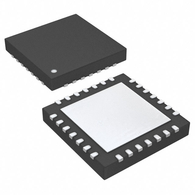


 工商网监
湘ICP备2023018690号
工商网监
湘ICP备2023018690号
