PIC16F526
Data Sheet
14-Pin, 8-Bit Flash Microcontroller
2010 Microchip Technology Inc.
DS41326E
�Note the following details of the code protection feature on Microchip devices:
•
Microchip products meet the specification contained in their particular Microchip Data Sheet.
•
Microchip believes that its family of products is one of the most secure families of its kind on the market today, when used in the
intended manner and under normal conditions.
•
There are dishonest and possibly illegal methods used to breach the code protection feature. All of these methods, to our
knowledge, require using the Microchip products in a manner outside the operating specifications contained in Microchip’s Data
Sheets. Most likely, the person doing so is engaged in theft of intellectual property.
•
Microchip is willing to work with the customer who is concerned about the integrity of their code.
•
Neither Microchip nor any other semiconductor manufacturer can guarantee the security of their code. Code protection does not
mean that we are guaranteeing the product as “unbreakable.”
Code protection is constantly evolving. We at Microchip are committed to continuously improving the code protection features of our
products. Attempts to break Microchip’s code protection feature may be a violation of the Digital Millennium Copyright Act. If such acts
allow unauthorized access to your software or other copyrighted work, you may have a right to sue for relief under that Act.
Information contained in this publication regarding device
applications and the like is provided only for your convenience
and may be superseded by updates. It is your responsibility to
ensure that your application meets with your specifications.
MICROCHIP MAKES NO REPRESENTATIONS OR
WARRANTIES OF ANY KIND WHETHER EXPRESS OR
IMPLIED, WRITTEN OR ORAL, STATUTORY OR
OTHERWISE, RELATED TO THE INFORMATION,
INCLUDING BUT NOT LIMITED TO ITS CONDITION,
QUALITY, PERFORMANCE, MERCHANTABILITY OR
FITNESS FOR PURPOSE. Microchip disclaims all liability
arising from this information and its use. Use of Microchip
devices in life support and/or safety applications is entirely at
the buyer’s risk, and the buyer agrees to defend, indemnify and
hold harmless Microchip from any and all damages, claims,
suits, or expenses resulting from such use. No licenses are
conveyed, implicitly or otherwise, under any Microchip
intellectual property rights.
Trademarks
The Microchip name and logo, the Microchip logo, dsPIC,
KEELOQ, KEELOQ logo, MPLAB, PIC, PICmicro, PICSTART,
PIC32 logo, rfPIC and UNI/O are registered trademarks of
Microchip Technology Incorporated in the U.S.A. and other
countries.
FilterLab, Hampshire, HI-TECH C, Linear Active Thermistor,
MXDEV, MXLAB, SEEVAL and The Embedded Control
Solutions Company are registered trademarks of Microchip
Technology Incorporated in the U.S.A.
Analog-for-the-Digital Age, Application Maestro, CodeGuard,
dsPICDEM, dsPICDEM.net, dsPICworks, dsSPEAK, ECAN,
ECONOMONITOR, FanSense, HI-TIDE, In-Circuit Serial
Programming, ICSP, Mindi, MiWi, MPASM, MPLAB Certified
logo, MPLIB, MPLINK, mTouch, Octopus, Omniscient Code
Generation, PICC, PICC-18, PICDEM, PICDEM.net, PICkit,
PICtail, REAL ICE, rfLAB, Select Mode, Total Endurance,
TSHARC, UniWinDriver, WiperLock and ZENA are
trademarks of Microchip Technology Incorporated in the
U.S.A. and other countries.
SQTP is a service mark of Microchip Technology Incorporated
in the U.S.A.
All other trademarks mentioned herein are property of their
respective companies.
© 2010, Microchip Technology Incorporated, Printed in the
U.S.A., All Rights Reserved.
Printed on recycled paper.
ISBN: 978-1-60932-355-4
Microchip received ISO/TS-16949:2002 certification for its worldwide
headquarters, design and wafer fabrication facilities in Chandler and
Tempe, Arizona; Gresham, Oregon and design centers in California
and India. The Company’s quality system processes and procedures
are for its PIC® MCUs and dsPIC® DSCs, KEELOQ® code hopping
devices, Serial EEPROMs, microperipherals, nonvolatile memory and
analog products. In addition, Microchip’s quality system for the design
and manufacture of development systems is ISO 9001:2000 certified.
DS41326E-page 2
2010 Microchip Technology Inc.
�PIC16F526
14-Pin, 8-Bit Flash Microcontroller
High-Performance RISC CPU:
Low-Power Features/CMOS Technology:
• Only 33 Single-Word Instructions
• All Single-Cycle Instructions except for Program
Branches which are Two-Cycle
• Two-Level Deep Hardware Stack
• Direct, Indirect and Relative Addressing modes
for Data and Instructions
• Operating Speed:
- DC – 20 MHz crystal oscillator
- DC – 200 ns instruction cycle
• On-chip Flash Program Memory:
- 1024 x 12
• General Purpose Registers (SRAM):
- 67 x 8
• Flash Data Memory:
- 64 x 8
• Standby current:
- 100 nA @ 2.0V, typical
• Operating current:
- 11 A @ 32 kHz, 2.0V, typical
- 175 A @ 4 MHz, 2.0V, typical
• Watchdog Timer current:
- 1 A @ 2.0V, typical
- 7 A @ 5.0V, typical
• High Endurance Program and Flash Data Memory
cells:
- 100,000 write Program Memory endurance
- 1,000,000 write Flash Data Memory endurance
- Program and Flash Data retention: >40 years
• Fully Static Design
• Wide Operating Voltage Range: 2.0V to 5.5V:
- Wide temperature range
- Industrial: -40C to +85C
- Extended: -40C to +125C
Special Microcontroller Features:
• 8 MHz Precision Internal Oscillator:
- Factory calibrated to ±1%
• In-Circuit Serial Programming™ (ICSP™)
• In-Circuit Debugging (ICD) Support
• Power-On Reset (POR)
• Device Reset Timer (DRT)
• Watchdog Timer (WDT) with Dedicated On-Chip
RC Oscillator for Reliable Operation
• Programmable Code Protection
• Multiplexed MCLR Input Pin
• Internal Weak Pull-ups on I/O Pins
• Power-Saving Sleep mode
• Wake-Up from Sleep on Pin Change
• Selectable Oscillator Options:
- INTRC: 4 MHz or 8 MHz precision Internal
RC oscillator
- EXTRC: External low-cost RC oscillator
- XT:
Standard crystal/resonator
- HS:
High-speed crystal/resonator
- LP:
Power-saving, low-frequency crystal
- EC:
High-speed external clock input
Device
PIC16F526
Program
Memory
Peripheral Features:
• 12 I/O Pins:
- 11 I/O pins with individual direction control
- 1 input-only pin
- High current sink/source for direct LED drive
- Wake-up on change
- Weak pull-ups
• 8-bit Real-time Clock/Counter (TMR0) with 8-bit
Programmable Prescaler
• Two Analog Comparators:
- Comparator inputs and output accessible
externally
- One comparator with 0.6V fixed on-chip
absolute voltage reference (VREF)
- One comparator with programmable on-chip
voltage reference (VREF)
• Analog-to-Digital (A/D) Converter:
- 8-bit resolution
- 3-channel external programmable inputs
- 1-channel internal input to internal absolute
0.6 voltage reference
Data Memory
Flash (words)
SRAM (bytes)
Flash
(bytes)
1024
67
64
2010 Microchip Technology Inc.
I/O
Comparators
Timers 8-bit
8-bit A/D
Channels
12
2
1
3
DS41326E-page 3
�PIC16F526
VDD
1
RB5/OSC1/CLKIN
2
3
RB4/OSC2/CLKOUT
RC5/T0CKI
4
5
RC4/C2OUT
6
RC3
7
RB3/MCLR/VPP
VSS
12
RB1/C1IN-/AN1/ICSPCLK
11
RB2/C1OUT/AN2
10
RC0/C2IN+
9
RC1/C2IN-
8
RC2/CVREF
RB0/C1IN+/AN0/ICSPDAT
3
RC5/T0CKI
4
NC
GND
RB1/C1IN-/AN1/ICSPCLK
10
RB2/C1OUT/AN2
9
5
6
7
8
RC1/C2IN-
2
RB3/MCLR/VPP
RB0/C1IN+/AN0/ICSPDAT
11
RC2/CVREF
RB4/OSC2/CLKOUT
PIC16F526
16 15 14 13
12
RC3
1
RC4/C2OUT
RB5/OSC1/CLKIN
DS41326E-page 4
14
13
16-PIN QFN DIAGRAM
VDD
FIGURE 1-2:
PIC16F526
14-PIN PDIP, SOIC, TSSOP DIAGRAM
NC
FIGURE 1-1:
RC0/C2IN+
2010 Microchip Technology Inc.
�PIC16F526
Table of Contents
1.0 General Description..................................................................................................................................................................... 7
2.0 PIC16F526 Device Varieties ...................................................................................................................................................... 9
3.0 Architectural Overview .............................................................................................................................................................. 11
4.0 Memory Organization ................................................................................................................................................................ 15
5.0 Flash Data Memory Control ...................................................................................................................................................... 23
6.0 I/O Port ...................................................................................................................................................................................... 27
7.0 Timer0 Module and TMR0 Register .......................................................................................................................................... 37
8.0 Special Features of the CPU..................................................................................................................................................... 43
9.0 Analog-to-Digital (A/D) Converter.............................................................................................................................................. 59
10.0 Comparator(s) ........................................................................................................................................................................... 63
11.0 Comparator Voltage Reference Module.................................................................................................................................... 69
12.0 Instruction Set Summary ........................................................................................................................................................... 71
13.0 Development Support................................................................................................................................................................ 79
14.0 Electrical Characteristics ........................................................................................................................................................... 83
15.0 DC and AC Characteristics Graphs and Charts ........................................................................................................................ 97
16.0 Packaging Information............................................................................................................................................................. 107
The Microchip Web Site .................................................................................................................................................................... 115
Customer Change Notification Service ............................................................................................................................................. 115
Customer Support ............................................................................................................................................................................. 115
Reader Response ............................................................................................................................................................................. 116
Index .................................................................................................................................................................................................. 117
Product Identification System................ ........................................................................................................................................... 119
TO OUR VALUED CUSTOMERS
It is our intention to provide our valued customers with the best documentation possible to ensure successful use of your Microchip products. To this end, we will continue to improve our publications to better suit your needs. Our publications will be refined
and enhanced as new volumes and updates are introduced.
If you have any questions or comments regarding this publication, please contact the Marketing Communications Department via
E-mail at docerrors@mail.microchip.com or fax the Reader Response Form in the back of this data sheet to (480) 792-4150.
We welcome your feedback.
Most Current Data Sheet
To obtain the most up-to-date version of this data sheet, please register at our Worldwide Web site at:
http://www.microchip.com
You can determine the version of a data sheet by examining its literature number found on the bottom outside corner of any page.
The last character of the literature number is the version number, (e.g., DS30000A is version A of document DS30000).
Errata
An errata sheet, describing minor operational differences from the data sheet and recommended workarounds, may exist for current
devices. As device/documentation issues become known to us, we will publish an errata sheet. The errata will specify the revision
of silicon and revision of document to which it applies.
To determine if an errata sheet exists for a particular device, please check with one of the following:
• Microchip’s Worldwide Web site; http://www.microchip.com
• Your local Microchip sales office (see last page)
• The Microchip Corporate Literature Center; U.S. FAX: (480) 792-7277
When contacting a sales office or the literature center, please specify which device, revision of silicon and data sheet (include literature number) you are using.
Customer Notification System
Register on our web site at www.microchip.com/cn to receive the most current information on all of our products.
2010 Microchip Technology Inc.
DS41326E-page 5
�PIC16F526
NOTES:
DS41326E-page 6
2010 Microchip Technology Inc.
�PIC16F526
1.0
GENERAL DESCRIPTION
The PIC16F526 device from Microchip Technology is
low-cost, high-performance, 8-bit, fully-static, Flashbased CMOS microcontrollers. It employs a RISC
architecture with only 33 single-word/single-cycle
instructions. All instructions are single cycle (200 s)
except for program branches, which take two cycles.
The PIC16F526 device delivers performance an order
of magnitude higher than their competitors in the same
price category. The 12-bit wide instructions are highly
symmetrical, resulting in a typical 2:1 code
compression over other 8-bit microcontrollers in its
class. The easy-to-use and easy to remember
instruction set reduces development time significantly.
The PIC16F526 product is equipped with special
features that reduce system cost and power
requirements. The Power-on Reset (POR) and Device
Reset Timer (DRT) eliminate the need for external
Reset circuitry. There are four oscillator configurations
to choose from, including INTRC Internal Oscillator
mode and the power-saving LP (Low-Power) Oscillator
mode. Power-Saving Sleep mode, Watchdog Timer
and code protection features improve system cost,
power and reliability.
1.1
Applications
The PIC16F526 device fits in applications ranging from
personal care appliances and security systems to lowpower remote transmitters/receivers. The Flash
technology makes customizing application programs
(transmitter codes, appliance settings, receiver
frequencies, etc.) extremely fast and convenient. The
small footprint packages, for through hole or surface
mounting, make these microcontrollers perfect for
applications with space limitations. Low cost, low
power, high performance, ease of use and I/O flexibility
make the PIC16F526 device very versatile even in
areas where no microcontroller use has been
considered before (e.g., timer functions, logic and
PLDs in larger systems and coprocessor applications).
The PIC16F526 device is available in the cost-effective
Flash programmable version, which is suitable for
production in any volume. The customer can take full
advantage of Microchip’s price leadership in Flash
programmable microcontrollers, while benefiting from
the Flash programmable flexibility.
The PIC16F526 product is supported by a full-featured
macro assembler, a software simulator, an in-circuit
emulator, a ‘C’ compiler, a low-cost development
programmer and a full featured programmer. All the
tools are supported on IBM® PC and compatible
machines.
TABLE 1-1:
FEATURES AND MEMORY OF PIC16F526
PIC16F526
Clock
Maximum Frequency of Operation (MHz)
Memory
Flash Program Memory
SRAM Data Memory (bytes)
Flash Data Memory (bytes)
Peripherals
Timer Module(s)
Wake-up from Sleep on Pin Change
Features
I/O Pins
Input Pins
20
1024
67
64
TMR0
Yes
11
1
Internal Pull-ups
Yes
In-Circuit Serial ProgrammingTM
Yes
Number of Instructions
Packages
33
14-pin PDIP, SOIC, TSSOP, QFN
The PIC16F526 device has Power-on Reset, selectable Watchdog Timer, selectable code-protect, high I/O current capability and
precision internal oscillator.
The PIC16F526 device uses serial programming with data pin RB0 and clock pin RB1.
2010 Microchip Technology Inc.
DS41326E-page 7
�PIC16F526
NOTES:
DS41326E-page 8
2010 Microchip Technology Inc.
�PIC16F526
2.0
PIC16F526 DEVICE VARIETIES
A variety of packaging options are available.
Depending
on
application
and
production
requirements, the proper device option can be selected
using the information in this section. When placing
orders, please use the PIC16F526 Product
Identification System at the back of this data sheet to
specify the correct part number.
2.1
Quick Turn Programming (QTP)
Devices
2.2
Serialized Quick Turn
ProgrammingSM (SQTPSM) Devices
Microchip offers a unique programming service, where
a few user-defined locations in each device are
programmed with different serial numbers. The serial
numbers may be random, pseudo-random or
sequential.
Serial programming allows each device to have a
unique number, which can serve as an entry code,
password or ID number.
Microchip offers a QTP programming service for
factory production orders. This service is made
available for users who choose not to program
medium-to-high quantity units and whose code
patterns have stabilized. The devices are identical to
the Flash devices but with all Flash locations and fuse
options already programmed by the factory. Certain
code and prototype verification procedures do apply
before production shipments are available. Please
contact your local Microchip Technology sales office for
more details.
2010 Microchip Technology Inc.
DS41326E-page 9
�PIC16F526
NOTES:
DS41326E-page 10
2010 Microchip Technology Inc.
�PIC16F526
3.0
ARCHITECTURAL OVERVIEW
The high performance of the PIC16F526 device can
be attributed to a number of architectural features
commonly found in RISC microprocessors. To begin
with, the PIC16F526 device uses a Harvard
architecture in which program and data are accessed
on separate buses. This improves bandwidth over
traditional von Neumann architectures where program
and data are fetched on the same bus. Separating
program and data memory further allows instructions
to be sized differently than the 8-bit wide data word.
Instruction opcodes are 12 bits wide, making it
possible to have all single-word instructions. A 12-bit
wide program memory access bus fetches a 12-bit
instruction in a single cycle. A two-stage pipeline
overlaps fetch and execution of instructions.
Consequently, all instructions (33) execute in a single
cycle (200 ns @ 20 MHz, 1 s @ 4 MHz) except for
program branches.
The PIC16F526 device contains an 8-bit ALU and
working register. The ALU is a general purpose arithmetic unit. It performs arithmetic and Boolean functions
between data in the working register and any register
file.
The ALU is 8 bits wide and capable of addition, subtraction, shift and logical operations. Unless otherwise
mentioned, arithmetic operations are two’s complement in nature. In two-operand instructions, one
operand is typically the W (working) register. The other
operand is either a file register or an immediate
constant. In single operand instructions, the operand is
either the W register or a file register.
The W register is an 8-bit working register used for ALU
operations. It is not an addressable register.
Table 3-1 below lists memory supported by the
PIC16F526 device.
Depending on the instruction executed, the ALU may
affect the values of the Carry (C), Digit Carry (DC) and
Zero (Z) bits in the STATUS register. The C and DC bits
operate as a borrow and digit borrow out bit,
respectively, in subtraction. See the SUBWF and ADDWF
instructions for examples.
TABLE 3-1:
A simplified block diagram is shown in Figure 3-2, with
the corresponding device pins described in Table 3-2.
Device
PIC16F526
PIC16F526 MEMORY
Program
Memory
Data Memory
Flash
(words)
SRAM
(bytes)
Flash
(bytes)
1024
67
64
The PIC16F526 device can directly or indirectly
address its register files and data memory. All Special
Function Registers (SFR), including the PC, are
mapped in the data memory. The PIC16F526 device
has a highly orthogonal (symmetrical) instruction set
that makes it possible to carry out any operation, on
any register, using any Addressing mode. This symmetrical nature and lack of “special optimal situations”
make programming with the PIC16F526 device simple,
yet efficient. In addition, the learning curve is reduced
significantly.
2010 Microchip Technology Inc.
DS41326E-page 11
�PIC16F526
FIGURE 3-1:
PIC16F526 BLOCK DIAGRAM
11
Flash Program
Memory
1K x 12
Flash Data
Memory
64x8
Program
Bus
8
Data Bus
Program Counter
PORTB
RB0/ICSPDAT
RB1/ICSPCLK
RB2
RB3/MCLR/VPP
RB4/OSC2/CLKOUT
RB5/OSC1/CLKIN
RAM
67
bytes
File
Registers
STACK1
STACK2
12
RAM Addr (1)
9
PORTC
Addr MUX
Instruction Reg
Direct Addr
5
5-7
RC0
RC1
RC2
RC3
RC4
RC5/T0CKI
Indirect
Addr
FSR Reg
STATUS Reg
8
Device Reset
Timer
OSC1/CLKIN
OSC2/CLKOUT
Instruction
Decode and
Control
Power-on
Reset
Timing
Generation
Watchdog
Timer
Internal RC
Clock
Comparator 1
3
MUX
C1IN+
C1INC1OUT
VREF
ALU
8
W Reg
Comparator 2
C2IN+
C2INC2OUT
CVREF
CVREF
CVREF
Timer0
MCLR
VDD, VSS
8-bit ADC
AN0
AN1
AN2
VREF
DS41326E-page 12
2010 Microchip Technology Inc.
�PIC16F526
TABLE 3-2:
PIC16F526 PINOUT DESCRIPTION
Name
RB0//C1IN+/AN0/
ICSPDAT
RB1/C1IN-/AN1/
ICSPCLK
RB2/C1OUT/AN2
RB3/MCLR/VPP
RB4/OSC2/CLKOUT
RB5/OSC1/CLKIN
RC0/C2IN+
RC1/C2INRC2/CVREF
RC3
RC4/C2OUT
RC5/T0CKI
Function
Input
Type
RB0
TTL
C1IN+
AN
Output
Type
Description
CMOS Bidirectional I/O pin. Can be software programmed for internal
weak pull-up and wake-up from Sleep on pin change.
—
Comparator 1 input.
—
ADC channel input.
AN0
AN
ICSPDAT
ST
CMOS ICSP™ mode Schmitt Trigger.
RB1
TTL
CMOS Bidirectional I/O pin. Can be software programmed for internal
weak pull-up and wake-up from Sleep on pin change.
C1IN-
AN
—
Comparator 1 input.
—
ADC channel input.
AN1
AN
ICSPCLK
ST
CMOS ICSP mode Schmitt Trigger.
RB2
TTL
CMOS Bidirectional I/O pin.
C1OUT
—
CMOS Comparator 1 output.
AN2
AN
—
ADC channel input.
RB3
TTL
—
Input pin. Can be software programmed for internal weak
pull-up and wake-up from Sleep on pin change.
MCLR
ST
—
Master Clear (Reset). When configured as MCLR, this pin is
an active-low Reset to the device. Voltage on MCLR/VPP must
not exceed VDD during normal device operation or the device
will enter Programming mode. Weak pull-up always on if
configured as MCLR.
VPP
HV
—
Programming voltage input.
RB4
TTL
OSC2
—
XTAL
CLKOUT
—
CMOS EXTRC/INTRC CLKOUT pin (FOSC/4).
RB5
TTL
OSC1
XTAL
CLKIN
ST
RC0
TTL
C2IN+
AN
RC1
TTL
C2IN-
AN
RC2
TTL
CVREF
—
RC3
TTL
CMOS Bidirectional I/O pin. Can be software programmed for internal
weak pull-up and wake-up from Sleep on pin change.
Oscillator crystal output. Connections to crystal or resonator in
Crystal Oscillator mode (XT, HS and LP modes only, PORTB
in other modes).
CMOS Bidirectional I/O pin.
—
Oscillator crystal input.
—
External clock source input.
CMOS Bidirectional I/O port.
—
Comparator 2 input.
CMOS Bidirectional I/O port.
—
Comparator 2 input.
CMOS Bidirectional I/O port.
AN
Programmable Voltage Reference output.
CMOS Bidirectional I/O port.
RC4
TTL
CMOS Bidirectional I/O port.
C2OUT
—
CMOS Comparator 2 output.
CMOS Bidirectional I/O port.
RC5
TTL
T0CKI
ST
—
Timer0 Schmitt Trigger input pin.
VDD
VDD
—
P
Positive supply for logic and I/O pins.
VSS
VSS
—
P
Ground reference for logic and I/O pins.
Legend: I = Input, O = Output, I/O = Input/Output, P = Power, — = Not used, TTL = TTL input,
ST = Schmitt Trigger input, HV = High Voltage
2010 Microchip Technology Inc.
DS41326E-page 13
�PIC16F526
3.1
Clocking Scheme/Instruction
Cycle
3.2
Instruction Flow/Pipelining
An instruction cycle consists of four Q cycles (Q1, Q2,
Q3 and Q4). The instruction fetch and execute are
pipelined such that fetch takes one instruction cycle,
while decode and execute take another instruction
cycle. However, due to the pipelining, each instruction
effectively executes in one cycle. If an instruction
causes the PC to change (e.g., GOTO), then two cycles
are required to complete the instruction (Example 3-1).
The clock input (OSC1/CLKIN pin) is internally divided
by four to generate four non-overlapping quadrature
clocks, namely Q1, Q2, Q3 and Q4. Internally, the PC
is incremented every Q1 and the instruction is fetched
from program memory and latched into the instruction
register in Q4. It is decoded and executed during the
following Q1 through Q4. The clocks and instruction
execution flow is shown in Figure 3-2 and Example 3-1.
A fetch cycle begins with the PC incrementing in Q1.
In the execution cycle, the fetched instruction is latched
into the Instruction Register (IR) in cycle Q1. This
instruction is then decoded and executed during the
Q2, Q3 and Q4 cycles. Data memory is read during Q2
(operand read) and written during Q4 (destination
write).
FIGURE 3-2:
CLOCK/INSTRUCTION CYCLE
Q1
Q2
Q3
Q4
Q1
Q2
Q3
Q4
Q1
Q2
Q3
Q4
OSC1
Q1
Q2
Internal
Phase
Clock
Q3
Q4
PC
PC
PC + 1
Fetch INST (PC)
Execute INST (PC – 1)
EXAMPLE 3-1:
PC + 2
Fetch INST (PC + 1)
Execute INST (PC)
Fetch INST (PC + 2)
Execute INST (PC + 1)
INSTRUCTION PIPELINE FLOW
1. MOVLW 03H
2. MOVWF PORTB
3. CALL SUB_1
4. BSF PORTB, BIT1
Fetch 1
Execute 1
Fetch 2
Execute 2
Fetch 3
Execute 3
Fetch 4
Flush
Fetch SUB_1 Execute SUB_1
All instructions are single cycle, except for any program branches. These take two cycles, since the fetch instruction
is “flushed” from the pipeline, while the new instruction is being fetched and then executed.
DS41326E-page 14
2010 Microchip Technology Inc.
�PIC16F526
4.1
Program Memory Organization for
the PIC16F526
The PIC16F526 device has an 11-bit Program Counter
(PC) capable of addressing a 2K x 12 program memory
space. Program memory is partitioned into user memory,
data memory and configuration memory spaces.
The user memory space is the on-chip user program
memory. As shown in Figure 4-1, it extends from 0x000
to 0x3FF and partitions into pages, including Reset
vector at address 0x3FF.
User Memory
Space
The PIC16F526 memories are organized into program
memory and data memory (SRAM).The self-writable
portion of the program memory called Flash data
memory is located at addresses at 400h-43Fh. All
Program mode commands that work on the normal
Flash memory work on the Flash data memory. This
includes bulk erase, row/column/cycling toggles, Load
and Read data commands (Refer to Section 5.0
“Flash Data Memory Control” for more details). For
devices with more than 512 bytes of program memory,
a paging scheme is used. Program memory pages are
accessed using one STATUS register bit. For the
PIC16F526, with data memory register files of more
than 32 registers, a banking scheme is used. Data
memory banks are accessed using the File Select
Register (FSR).
FIGURE 4-1:
Data Memory
Space
MEMORY ORGANIZATION
MEMORY MAP
On-chip User
Program
Memory (Page 0)
On-chip User
Program
Memory (Page 1)
Reset Vector
000h
1FFh
200h
3FEh
3FFh
400h
Flash Data Memory
User ID Locations
Backup OSCCAL
Locations
Configuration Memory
Space
4.0
43Fh
440h
443h
444h
447h
448h
Reserved
49Fh
4A0h
Unimplemented
7FEh
Configuration Word
7FFh
The data memory space is the Flash data memory
block and is located at addresses PC = 400h-43Fh. All
Program mode commands that work on the normal
Flash memory work on the Flash data memory block.
This includes bulk erase, Load and Read data
commands.
The configuration memory space extends from 0x440
to 0x7FF. Locations from 0x448 through 0x49F are
reserved. The user ID locations extend from 0x440
through 0x443. The Backup OSCCAL locations extend
from 0x444 through 0x447. The Configuration Word is
physically located at 0x7FF.
Refer to “PIC16F526 Memory Programming
Specification” (DS41317) for more details.
2010 Microchip Technology Inc.
DS41326E-page 15
�PIC16F526
4.2
Data Memory (SRAM and FSRs)
4.2.1
Data memory is composed of registers or bytes of
SRAM. Therefore, data memory for a device is
specified by its register file. The register file is divided
into two functional groups: Special Function Registers
(SFR) and General Purpose Registers (GPR).
The General Purpose Register file is accessed, either
directly or indirectly, through the File Select Register
(FSR). See Section 4.8 “Indirect Data Addressing:
INDF and FSR Registers”.
The Special Function Registers are registers used by
the CPU and peripheral functions for controlling
desired operations of the PIC16F526. See Figure 4-1
for details.
4.2.2
The Special Function Registers can be classified into
two sets. The Special Function Registers associated
with the “core” functions are described in this section.
Those related to the operation of the peripheral
features are described in the section for each
peripheral feature.
REGISTER FILE MAP
FSR
00
01
20h
File Address
10
40h
11
60h
00h
INDF(1)
INDF(1)
INDF(1)
INDF(1)
01h
TMR0
EECON
TMR0
EECON
02h
PCL
PCL
PCL
PCL
03h
STATUS
STATUS
STATUS
STATUS
04h
FSR
FSR
FSR
FSR
05h
OSCCAL
EEDATA
OSCCAL
EEDATA
06h
PORTB
EEADR
PORTB
EEADR
07h
PORTC
PORTC
PORTC
PORTC
08h
CM1CON0
CM1CON0
CM1CON0
CM1CON0
09h
ADCON0
ADCON0
ADCON0
ADCON0
0Ah
0Bh
ADRES
CM2CON0
ADRES
CM2CON0
ADRES
CM2CON0
ADRES
CM2CON0
0Ch
VRCON
VRCON
VRCON
VRCON
0Dh
General
Purpose
Registers
0Fh
10h
Addresses map back to
addresses in Bank 0.
4Fh
6Fh
2Fh
30h
General
Purpose
Registers
1Fh
50h
General
Purpose
Registers
3Fh
Bank 0
Note 1:
SPECIAL FUNCTION REGISTERS
The Special Function Registers (SFRs) are registers
used by the CPU and peripheral functions to control the
operation of the device (Table 4-1).
The PIC16F526 register file is composed of 16 Special
Function Registers and 67 General Purpose Registers.
FIGURE 4-2:
GENERAL PURPOSE REGISTER
FILE
70h
General
Purpose
Registers
5Fh
Bank 1
General
Purpose
Registers
7Fh
Bank 2
Bank 3
Not a physical register. See Section 4.8 “Indirect Data Addressing: INDF and FSR Registers”.
DS41326E-page 16
2010 Microchip Technology Inc.
�PIC16F526
TABLE 4-1:
Addr
SPECIAL FUNCTION REGISTER (SFR) SUMMARY
Name
Bit 7
Bit 6
—
—
Bit 5
Bit 4
Bit 3
Bit 2
Bit 1
Bit 0
Page #
N/A
TRIS
--11 1111
27
N/A
OPTION
Contains control bits to configure Timer0 and Timer0/WDT prescaler
1111 1111
19
00h
INDF
Uses contents of FSR to Address Data Memory (not a physical register)
xxxx xxxx
22
01h/41h
TMR0
Timer0 Module Register
xxxx xxxx
37
02h(1)
PCL
Low order 8 bits of PC
1111 1111
21
03h
STATUS
0001 1xxx
18
04h
FSR
05h/45h
OSCCAL
06h/46h
07h
08h
CM1CON0
09h
ADCON0
0Ah
ADRES
0Bh
CM2CON0
C2OUT
C2OUTEN
C2POL
RBWUF
I/O Control Register (PORTB, PORTC)
Value on
Power-on
Reset
CWUF
PA0
TO
PD
Z
DC
C
Indirect Data Memory Address Pointer
CAL4
CAL3
CAL2
CAL1
CAL0
100x xxxx
22
—
1111 111-
20
27
CAL6
CAL5
PORTB
—
—
RB5
RB4
RB3
RB2
RB1
RB0
--xx xxxx
PORTC
—
—
RC5
RC4
RC3
RC2
RC1
RC0
--xx xxxx
28
C1OUT
C1OUTEN
C1POL
C1T0CS
C1ON
C1NREF
C1PREF
C1WU
q111 1111
63
ANS1
ANS0
ADCS1
ADCS0
CHS1
CHS0
GO/DONE
ADON
1111 1100
61
ADC Conversion Result
C2PREF2
C2ON
xxxx xxxx
62
C2NREF
C2PREF1
C2WU
q111 1111
64
0Ch
VRCON
VREN
VROE
VRR
—
VR3
VR2
VR1
VR0
001- 1111
69
21h/61h
EECON
—
—
—
FREE
WRERR
WREN
WR
RD
---0 x000
23
25h/65h
EEDATA
26h/66h
EEADR
Legend:
x = unknown, u = unchanged, – = unimplemented, read as '0' (if applicable), q = value depends on condition.
Shaded cells = unimplemented or unused
The upper byte of the Program Counter is not directly accessible. See Section 4.6 “Program Counter” for an explanation of how to
access these bits.
Note 1:
SELF READ/WRITE DATA
—
2010 Microchip Technology Inc.
—
SELF READ/WRITE ADDRESS
xxxx xxxx
23
--xx xxxx
23
DS41326E-page 17
�PIC16F526
4.3
STATUS Register
For example, CLRF STATUS, will clear the upper three
bits and set the Z bit. This leaves the STATUS register
as 000u u1uu (where u = unchanged).
This register contains the arithmetic status of the ALU,
the Reset status and the page preselect bit.
Therefore, it is recommended that only BCF, BSF and
MOVWF instructions be used to alter the STATUS
register. These instructions do not affect the Z, DC or C
bits from the STATUS register. For other instructions
which do affect Status bits, see Section 12.0
“Instruction Set Summary”.
The STATUS register can be the destination for any
instruction, as with any other register. If the STATUS
register is the destination for an instruction that affects
the Z, DC or C bits, then the write to these three bits is
disabled. These bits are set or cleared according to the
device logic. Furthermore, the TO and PD bits are not
writable. Therefore, the result of an instruction with the
STATUS register as destination may be different than
intended.
REGISTER 4-1:
STATUS: STATUS REGISTER
R/W-0
R/W-0
R/W-0
R-1
R-1
R/W-x
R/W-x
R/W-x
RBWUF
CWUF
PA0
TO
PD
Z
DC
C
bit 7
bit 0
Legend:
R = Readable bit
W = Writable bit
U = Unimplemented bit, read as ‘0’
-n = Value at POR
‘1’ = Bit is set
‘0’ = Bit is cleared
x = Bit is unknown
bit 7
RBWUF: Wake-up from Sleep on Pin Change bit
1 = Reset due to wake-up from Sleep on pin change
0 = After power-up or other Reset
bit 6
CWUF: Wake-up from Sleep on Comparator Change bit
1 = Reset due to wake-up from Sleep on comparator change
0 = After power-up or other Reset
bit 5
PA0: Program Page Preselect bit
1 = Page 1 (000h-1FFh)
0 = Page 0 (200h-3FFh)
bit 4
TO: Time-out bit
1 = After power-up, CLRWDT instruction, or SLEEP instruction
0 = A WDT time-out occurred
bit 3
PD: Power-down bit
1 = After power-up or by the CLRWDT instruction
0 = By execution of the SLEEP instruction
bit 2
Z: Zero bit
1 = The result of an arithmetic or logic operation is zero
0 = The result of an arithmetic or logic operation is not zero
bit 1
DC: Digit carry/borrow bit (for ADDWF and SUBWF instructions)
ADDWF:
1 = A carry from the 4th low-order bit of the result occurred
0 = A carry from the 4th low-order bit of the result did not occur
SUBWF:
1 = A borrow from the 4th low-order bit of the result did not occur
0 = A borrow from the 4th low-order bit of the result occurred
bit 0
C: Carry/borrow bit (for ADDWF, SUBWF and RRF, RLF instructions)
ADDWF:
SUBWF:
RRF or RLF:
1 = A carry occurred
1 = A borrow did not occur
Load bit with LSb or MSb, respectively
0 = A carry did not occur 0 = A borrow occurred
DS41326E-page 18
2010 Microchip Technology Inc.
�PIC16F526
4.4
OPTION Register
The OPTION register is a 8-bit wide, write-only register,
which contains various control bits to configure the
Timer0/WDT prescaler and Timer0.
Note:
By executing the OPTION instruction, the contents of
the W register will be transferred to the OPTION
register. A Reset sets the OPTION bits.
REGISTER 4-2:
If TRIS bit is set to ‘0’, the wake-up on
change and pull-up functions are disabled
for that pin (i.e., note that TRIS overrides
Option control of RBPU and RBWU).
OPTION: OPTION REGISTER
W-1
W-1
W-1
W-1
W-1
W-1
W-1
W-1
RBWU
RBPU
T0CS(1)
T0SE
PSA
PS2
PS1
PS0
bit 7
bit 0
Legend:
R = Readable bit
W = Writable bit
U = Unimplemented bit, read as ‘0’
-n = Value at POR
‘1’ = Bit is set
‘0’ = Bit is cleared
bit 7
RBWU: Enable Wake-up On Pin Change bit (RB0, RB1, RB3, RB4)
1 = Disabled
0 = Enabled
bit 6
RBPU: Enable Weak Pull-ups bit (RB0, RB1, RB3, RB4)
1 = Disabled
0 = Enabled
bit 5
T0CS: Timer0 Clock Source Select bit(1)
1 = Transition on T0CKI pin
0 = Internal instruction cycle clock (CLKOUT)
bit 4
T0SE: Timer0 Source Edge Select bit
1 = Increment on high-to-low transition on T0CKI pin
0 = Increment on low-to-high transition on T0CKI pin
bit 3
PSA: Prescaler Assignment bit
1 = Prescaler assigned to the WDT
0 = Prescaler assigned to Timer0
bit 2-0
PS: Prescaler Rate Select bits
Note 1:
Bit Value
Timer0 Rate
WDT Rate
000
001
010
011
100
101
110
111
1:2
1:4
1:8
1 : 16
1 : 32
1 : 64
1 : 128
1 : 256
1:1
1:2
1:4
1:8
1 : 16
1 : 32
1 : 64
1 : 128
x = Bit is unknown
If the T0CS bit is set to ‘1’, it will override the TRIS function on the T0CKI pin.
2010 Microchip Technology Inc.
DS41326E-page 19
�PIC16F526
4.5
OSCCAL Register
The Oscillator Calibration (OSCCAL) register is used
to calibrate the 8 MHz internal oscillator macro. It
contains 7 bits of calibration that uses a two’s
complement scheme for controlling the oscillator speed.
See Register 4-3 for details.
REGISTER 4-3:
OSCCAL: OSCILLATOR CALIBRATION REGISTER
R/W-1
R/W-1
R/W-1
R/W-1
R/W-1
R/W-1
R/W-1
U-0
CAL6
CAL5
CAL4
CAL3
CAL2
CAL1
CAL0
—
bit 7
bit 0
Legend:
R = Readable bit
W = Writable bit
U = Unimplemented bit, read as ‘0’
-n = Value at POR
‘1’ = Bit is set
‘0’ = Bit is cleared
bit 7-1
CAL: Oscillator Calibration bits
0111111 = Maximum frequency
•
•
•
0000001
0000000 = Center frequency
1111111
•
•
•
1000000 = Minimum frequency
bit 0
Unimplemented: Read as ‘0’
DS41326E-page 20
x = Bit is unknown
2010 Microchip Technology Inc.
�PIC16F526
4.6
Program Counter
4.6.1
EFFECTS OF RESET
As a program instruction is executed, the Program
Counter (PC) will contain the address of the next
program instruction to be executed. The PC value is
increased by one every instruction cycle, unless an
instruction changes the PC.
The PC is set upon a Reset, which means that the PC
addresses the last location in the last page (i.e., the
oscillator calibration instruction). After executing
MOVLW XX, the PC will roll over to location 00h and
begin executing user code.
For a GOTO instruction, bits 8:0 of the PC are provided
by the GOTO instruction word. The Program Counter
(PCL) is mapped to PC. Bit 5 of the STATUS
register provides page information to bit 9 of the PC
(Figure 4-3).
The STATUS register page preselect bits are cleared
upon a Reset, which means that page 0 is pre-selected.
For a CALL instruction, or any instruction where the
PCL is the destination, bits 7:0 of the PC again are
provided by the instruction word. However, PC
does not come from the instruction word, but is always
cleared (Figure 4-3).
Instructions where the PCL is the destination, or modify
PCL instructions, include MOVWF PCL, ADDWF PCL
and BSF PCL,5.
Note:
Because bit 8 of the PC is cleared in the
CALL instruction or any modify PCL
instruction, all subroutine calls or computed jumps are limited to the first 256
locations of any program memory page
(512 words long).
FIGURE 4-3:
LOADING OF PC
BRANCH INSTRUCTIONS
GOTO Instruction
10 9 8 7
PC
0
PCL
PA0
4.7
Stack
The PIC16F526 device has a 2-deep, 12-bit wide
hardware PUSH/POP stack.
A CALL instruction will PUSH the current value of Stack 1
into Stack 2 and then PUSH the current PC value, incremented by one, into Stack Level 1. If more than two
sequential CALLs are executed, only the most recent two
return addresses are stored.
A RETLW instruction will POP the contents of Stack
Level 1 into the PC and then copy Stack Level 2
contents into Stack Level 1. If more than two sequential
RETLWs are executed, the stack will be filled with the
address previously stored in Stack Level 2. Note that
the W register will be loaded with the literal value
specified in the instruction. This is particularly useful for
the implementation of data look-up tables within the
program memory.
Note 1: There are no Status bits to indicate Stack
Overflows or Stack Underflow conditions.
2: There are no instruction mnemonics
called PUSH or POP. These are actions
that occur from the execution of the CALL
and RETLW instructions.
Instruction Word
7
Therefore, upon a Reset, a GOTO instruction will
automatically cause the program to jump to page 0 until
the value of the page bits is altered.
0
Status
CALL or Modify PCL Instruction
10 9 8 7
PC
0
PCL
7
Instruction Word
Reset to ‘0’
PA0
0
Status
2010 Microchip Technology Inc.
DS41326E-page 21
�PIC16F526
4.8
Indirect Data Addressing: INDF
and FSR Registers
A simple program to clear RAM locations 10h-1Fh
using indirect addressing is shown in Example 4-1.
The INDF Register is not a physical register.
Addressing INDF actually addresses the register
whose address is contained in the FSR Register (FSR
is a pointer). This is indirect addressing.
EXAMPLE 4-1:
Reading INDF itself indirectly (FSR = 0) will produce
00h. Writing to the INDF Register indirectly results in a
no-operation (although Status bits may be affected).
MOVLW
MOVWF
CLRF
NEXT
INCF
BTFSC
GOTO
CONTINUE
:
:
The FSR is an 8-bit wide register. It is used in
conjunction with the INDF Register to indirectly
address the data memory area.
The FSR bits are used to select data memory
addresses 00h to 1Fh.
HOW TO CLEAR RAM
USING INDIRECT
ADDRESSING
0x10
FSR
INDF
;initialize pointer
;to RAM
;clear INDF
;register
;inc pointer
;all done?
;NO, clear next
FSR,F
FSR,4
NEXT
;YES, continue
FSR are the bank select bits and are used to
select the bank to be addressed (00 = Bank 0,
01 = Bank 1, 10 = Bank 2, 11 = Bank 3).
FSR is unimplemented and read as ‘1’.
FIGURE 4-4:
(FSR)
6
DIRECT/INDIRECT ADDRESSING
Direct Addressing
(opcode)
4
5
bank select
3
2
1
Indirect Addressing
(FSR)
0
6
location select
00
01
10
11
5
4
bank
select
3
2
1
0
location select
00h
Data
Memory(1)
0Ch
0Dh
Addresses map back to
addresses in Bank 0.
0Fh
10h
2Fh
4Fh
6Fh
1Fh
3Fh
5Fh
7Fh
Bank 0
Bank 1
Bank 2
Bank 3
Note 1: For register map detail see Figure 4-1.
DS41326E-page 22
2010 Microchip Technology Inc.
�PIC16F526
5.0
FLASH DATA MEMORY
CONTROL
The Flash data memory is readable and writable during
normal operation (full VDD range). This memory is not
directly mapped in the register file space. Instead, it is
indirectly addressed through the Special Function
Registers (SFRs).
5.1
Reading Flash Data Memory
To read a Flash data memory location the user must:
• Write the EEADR register
• Set the RD bit of the EECON register
The value written to the EEADR register determines
which Flash data memory location is read. Setting the
RD bit of the EECON register initiates the read. Data
from the Flash data memory read is available in the
EEDATA register immediately. The EEDATA register
will hold this value until another read is initiated or it is
modified by a write operation. Program execution is
suspended while the read cycle is in progress.
Execution will continue with the instruction following the
one that sets the WR bit. See Example 1 for sample
code.
EXAMPLE 1:
READING FROM FLASH
DATA MEMORY
BANKSEL EEADR
;
MOVF DATA_EE_ADDR, W
;
MOVWF EEADR
;Data Memory
BANKSEL EECON1
;
;Address to read
BSF EECON, RD
;EE Read
MOVF EEDATA, W
;W = EEDATA
Note: Only a BSF command will work to enable the
Flash data memory read documented in
Example 1. No other sequence of
commands will work, no exceptions.
5.2
Writing and Erasing Flash Data
Memory
Flash data memory is erased one row at a time and
written one byte at a time. The 64-byte array is made
up of eight rows. A row contains eight sequential bytes.
Row boundaries exist every eight bytes.
Generally, the procedure to write a byte of data to Flash
data memory is:
1.
2.
Identify the row containing the address where
the byte will be written.
If there is other information in that row that must
be saved, copy those bytes from Flash data
memory to RAM.
2010 Microchip Technology Inc.
3.
4.
Perform a row erase of the row of interest.
Write the new byte of data and any saved bytes
back to the appropriate addresses in Flash data
memory.
To prevent accidental corruption of the Flash data
memory, an unlock sequence is required to initiate a
write or erase cycle. This sequence requires that the bit
set instructions used to configure the EECON register
happen exactly as shown in Example 2 and Example 3,
depending on the operation requested.
5.2.1
ERASING FLASH DATA MEMORY
A row must be manually erased before writing new
data. The following sequence must be performed for a
single row erase.
1.
2.
3.
4.
Load EEADR with an address in the row to be
erased.
Set the FREE bit to enable the erase.
Set the WREN bit to enable write access to the
array.
Set the WR bit to initiate the erase cycle.
If the WREN bit is not set in the instruction cycle after
the FREE bit is set, the FREE bit will be cleared in
hardware.
If the WR bit is not set in the instruction cycle after the
WREN bit is set, the WREN bit will be cleared in
hardware.
Sample code that follows this procedure is included in
Example 2.
Program execution is suspended while the erase cycle
is in progress. Execution will continue with the
instruction following the one that sets the WR bit.
EXAMPLE 2:
ERASING A FLASH DATA
MEMORY ROW
BANKSEL
EEADR
MOVLW
EE_ADR_ERASE
; LOAD ADDRESS OF ROW TO
MOVWF
EEADR
;
BSF
EECON,FREE
; SELECT ERASE
BSF
EECON,WREN
; ENABLE WRITES
BSF
EECON,WR
; INITITATE ERASE
; ERASE
Note 1: The FREE bit may be set by any command normally used by the core. However, the WREN and WR bits can only be
set using a series of BSF commands, as
documented in Example 1. No other
sequence of commands will work, no
exceptions.
2: Bits of the EEADR register indicate
which row is to be erased.
DS41326E-page 23
�PIC16F526
5.2.2
WRITING TO FLASH DATA
MEMORY
Note 1: Only a series of BSF commands will work
to enable the memory write sequence
documented in Example 2. No other
sequence of commands will work, no
exceptions.
Once a cell is erased, new data can be written.
Program execution is suspended during the write cycle.
The following sequence must be performed for a single
byte write.
1.
2.
3.
4.
2: For reads, erases and writes to the Flash
data memory, there is no need to insert a
NOP into the user code as is done on midrange devices. The instruction immediately
following the “BSF EECON,WR/RD” will be
fetched and executed properly.
Load EEADR with the address.
Load EEDATA with the data to write.
Set the WREN bit to enable write access to the
array.
Set the WR bit to initiate the erase cycle.
If the WR bit is not set in the instruction cycle after the
WREN bit is set, the WREN bit will be cleared in
hardware.
Sample code that follows this procedure is included in
Example 3.
EXAMPLE 3:
BANKSEL
MOVLW
MOVWF
MOVLW
MOVWF
BSF
BSF
WRITING A FLASH DATA
MEMORY ROW
EEADR
EE_ADR_WRITE
EEADR
EE_DATA_TO_WRITE
EEDATA
EECON,WREN
EECON,WR
;
;
;
;
;
;
5.3
Write Verify
Depending on the application, good programming
practice may dictate that data written to the Flash data
memory be verified. Example 4 is an example of a write
verify.
EXAMPLE 4:
LOAD ADDRESS
WRITE VERIFY OF FLASH
DATA MEMORY
MOVF
EEDATA, W
;EEDATA has not changed
BSF
EECON, RD
;Read the value written
;from previous write
LOAD DATA
INTO EEDATA REGISTER
ENABLE WRITES
INITITATE ERASE
XORWF
EEDATA, W
;
BTFSS
STATUS, Z
;Is data the same
GOTO
WRITE_ERR
;No, handle error
;Yes, continue
REGISTER 5-1:
EEDATA: FLASH DATA REGISTER
R/W-x
R/W-x
R/W-x
R/W-x
R/W-x
R/W-x
R/W-x
R/W-x
EEDATA7
EEDATA6
EEDATA5
EEDATA4
EEDATA3
EEDATA2
EEDATA1
EEDATA0
bit 7
bit 0
Legend:
R = Readable bit
W = Writable bit
U = Unimplemented bit, read as ‘0’
-n = Value at POR
‘1’ = Bit is set
‘0’ = Bit is cleared
bit 7-0
x = Bit is unknown
EEDATA: 8-bits of data to be read from/written to data Flash
REGISTER 5-2:
EEADR: FLASH ADDRESS REGISTER
U-0
U-0
R/W-x
R/W-x
R/W-x
R/W-x
R/W-x
R/W-x
—
—
EEADR5
EEADR4
EEADR3
EEADR2
EEADR1
EEADR0
bit 7
bit 0
Legend:
R = Readable bit
W = Writable bit
U = Unimplemented bit, read as ‘0’
-n = Value at POR
‘1’ = Bit is set
‘0’ = Bit is cleared
bit 7-6
Unimplemented: Read as ‘0’.
bit 5-0
EEADR: 6-bits of data to be read from/written to data Flash
DS41326E-page 24
x = Bit is unknown
2010 Microchip Technology Inc.
�PIC16F526
REGISTER 5-3:
EECON: FLASH CONTROL REGISTER
U-0
U-0
U-0
R/W-0
R/W-0
R/W-0
R/W-0
R/W-0
—
—
—
FREE
WRERR
WREN
WR
RD
bit 7
bit 0
Legend:
S = Bit can only be set
R = Readable bit
W = Writable bit
U = Unimplemented bit, read as ‘0’
-n = Value at POR
‘1’ = Bit is set
‘0’ = Bit is cleared
x = Bit is unknown
bit 7-5
Unimplemented: Read as ‘0’.
bit 4
FREE: Flash Data Memory Row Erase Enable Bit
1 = Program memory row being pointed to by EEADR will be erased on the next write cycle. No write
will be performed. This bit is cleared at the completion of the erase operation.
0 = Perform write only
bit 3
WRERR: Write Error Flag bit
1 = A write operation terminated prematurely (by device Reset)
0 = Write operation completed successfully
bit 2
WREN: Write Enable bit
1 = Allows write cycle to Flash data memory
0 = Inhibits write cycle to Flash data memory
bit 1
WR: Write Control bit
1 = Initiate a erase or write cycle
0 = Write/Erase cycle is complete
bit 0
RD: Read Control bit
1 = Initiate a read of Flash data memory
0 = Do not read Flash data memory
5.4
Code Protection
Code protection does not prevent the CPU from
performing read or write operations on the Flash data
memory. Refer to the code protection chapter for more
information.
2010 Microchip Technology Inc.
DS41326E-page 25
�PIC16F526
NOTES:
DS41326E-page 26
2010 Microchip Technology Inc.
�PIC16F526
6.0
I/O PORT
6.2
PORTC is a 6-bit I/O register. Only the low-order 6 bits
are used (RC). Bits 7 and 6 are unimplemented
and read as ‘0’s.
As with any other register, the I/O register(s) can be
written and read under program control. However, read
instructions (e.g., MOVF PORTB,W) always read the I/O
pins independent of the pin’s Input/Output modes. On
Reset, all I/O ports are defined as input (inputs are at highimpedance) since the I/O control registers are all set.
6.1
6.3
TRIS Register
The Output Driver Control register is loaded with the
contents of the W register by executing the TRIS f
instruction. A ‘1’ from a TRIS register bit puts the
corresponding output driver in a High-Impedance
mode. A ‘0’ puts the contents of the output data latch
on the selected pins, enabling the output buffer. The
exceptions are RB3, which is input-only and the T0CKI
pin, which may be controlled by the OPTION register.
See Register 4-2.
PORTB
PORTB is a 6-bit I/O register. Only the low-order 6 bits
are used (RB). Bits 7 and 6 are unimplemented
and read as ‘0’s. Please note that RB3 is an input-only
pin. The Configuration Word can set several I/O’s to
alternate functions. When acting as alternate functions,
the pins will read as ‘0’ during a port read. Pins RB0,
RB1, RB3 and RB4 can be configured with weak pullups and also for wake-up on change. The wake-up on
change and weak pull-up functions are not pin
selectable. If RB3/MCLR is configured as MCLR, weak
pull-up is always on and wake-up on change for this pin
is not enabled.
TABLE 6-1:
PORTC
TRIS registers are “write-only”. Active bits in these
registers are set (output drivers disabled) upon Reset.
WEAK PULL-UP ENABLED PINS
Device
RB0 Weak Pull-up
PIC16F526
Yes
RB1 Weak Pull-up RB3 Weak Pull-up(1)
Yes
RB4 Weak Pull-up
Yes
Yes
Note 1: When MCLREN = 1, the weak pull-up on RB3/MCLR is always enabled.
REGISTER 6-1:
PORTB: PORTB REGISTER
U-0
U-0
R/W-x
R/W-x
R/W-x
R/W-x
R/W-x
R/W-x
—
—
RB5
RB4
RB3
RB2
RB1
RB0
bit 7
bit 0
Legend:
R = Readable bit
W = Writable bit
U = Unimplemented bit, read as ‘0’
-n = Value at POR
‘1’ = Bit is set
‘0’ = Bit is cleared
bit 7-6
Unimplemented: Read as ‘0’
bit 5-0
RB: PORTB I/O Pin bits
1 = Port pin is >VIH min.
0 = Port pin is VIH min.
0 = Port pin is 4.5V, C1 = C2 30 pF is
recommended.
These values are for design guidance
only. Rs may be required to avoid overdriving crystals with low drive level specification. Since each crystal has its own
characteristics, the user should consult
the crystal manufacturer for appropriate
values of external components.
EXTERNAL CRYSTAL OSCILLATOR
CIRCUIT
Either a prepackaged oscillator or a simple oscillator
circuit with TTL gates can be used as an external
crystal oscillator circuit. Prepackaged oscillators
provide a wide operating range and better stability. A
well-designed crystal oscillator will provide good
performance with TTL gates. Two types of crystal
oscillator circuits can be used: one with parallel
resonance, or one with series resonance.
Figure 8-3 shows implementation of a parallel resonant
oscillator circuit. The circuit is designed to use the
fundamental frequency of the crystal. The 74AS04
inverter performs the 180-degree phase shift that a
parallel oscillator requires. The 4.7 k resistor provides
the negative feedback for stability. The 10 k
potentiometers bias the 74AS04 in the linear region.
This circuit could be used for external oscillator
designs.
FIGURE 8-3:
EXTERNAL PARALLEL
RESONANT CRYSTAL
OSCILLATOR CIRCUIT
+5V
To Other
Devices
10k
74AS04
4.7k
CLKIN
74AS04
PIC16F526
10k
XTAL
Figure 8-4 shows a series resonant oscillator circuit.
This circuit is also designed to use the fundamental
frequency of the crystal. The inverter performs a 180degree phase shift in a series resonant oscillator
circuit. The 330 resistors provide the negative
feedback to bias the inverters in their linear region.
FIGURE 8-4:
330
EXTERNAL SERIES
RESONANT CRYSTAL
OSCILLATOR CIRCUIT
To Other
Devices
330
74AS04
74AS04
74AS04
CLKIN
0.1 mF
PIC16F526
XTAL
8.2.4
EXTERNAL RC OSCILLATOR
For timing insensitive applications, the RC device
option offers additional cost savings. The RC oscillator
frequency is a function of the supply voltage, the resistor (REXT) and capacitor (CEXT) values, and the operating temperature. In addition to this, the oscillator
frequency will vary from unit-to-unit due to normal process parameter variation. Furthermore, the difference
in lead frame capacitance between package types will
also affect the oscillation frequency, especially for low
CEXT values. The user also needs to take into account
variation due to tolerance of external R and C
components used.
Figure 8-5 shows how the R/C combination is connected to the PIC16F526 device. For REXT values
below 3.0 k, the oscillator operation may become
unstable, or stop completely. For very high REXT values
(e.g., 1 M), the oscillator becomes sensitive to noise,
humidity and leakage. Thus, we recommend keeping
REXT between 5.0 k and 100 k.
Although the oscillator will operate with no external
capacitor (CEXT = 0 pF), we recommend using values
above 20 pF for noise and stability reasons. With no or
small external capacitance, the oscillation frequency
can vary dramatically due to changes in external
capacitances, such as PCB trace capacitance or
package lead frame capacitance.
Section 14.0 “Electrical Characteristics” shows RC
frequency variation from part-to-part due to normal
process variation. The variation is larger for larger values of R (since leakage current variation will affect RC
frequency more for large R) and for smaller values of C
(since variation of input capacitance will affect RC
frequency more).
10k
20 pF
DS41326E-page 46
20 pF
2010 Microchip Technology Inc.
�PIC16F526
Also, see the Electrical Specifications section for
variation of oscillator frequency due to VDD for given
REXT/CEXT values, as well as frequency variation due
to operating temperature for given R, C and VDD
values.
FIGURE 8-5:
EXTERNAL RC
OSCILLATOR MODE
VDD
REXT
OSC1
Internal
clock
N
CEXT
PIC16F526
VSS
FOSC/4
OSC2/CLKOUT
8.2.5
INTERNAL 4/8 MHz RC
OSCILLATOR
The internal RC oscillator provides a fixed 4/8 MHz
(nominal) system clock at VDD = 5V and 25°C, (see
Section 14.0 “Electrical Characteristics” for
information on variation over voltage and temperature).
In addition, a calibration instruction is programmed into
the last address of memory, which contains the calibration value for the internal RC oscillator. This location is
always non-code protected, regardless of the codeprotect settings. This value is programmed as a MOVLW
XX instruction where XX is the calibration value, and is
placed at the Reset vector. This will load the W register
with the calibration value upon Reset and the PC will
then roll over to the users program at address 0x000.
The user then has the option of writing the value to the
OSCCAL Register (05h) or ignoring it.
OSCCAL, when written to with the calibration value, will
“trim” the internal oscillator to remove process variation
from the oscillator frequency.
Note:
Erasing the device will also erase the preprogrammed internal calibration value for
the internal oscillator. The calibration
value must be read prior to erasing the
part so it can be reprogrammed correctly
later.
For the PIC16F526 device, only bits 7:1 of OSCCAL
are used for calibration. See Register 4-3 for more
information.
Note:
2010 Microchip Technology Inc.
The bit 0 of the OSCCAL register is
unimplemented and should be written as
‘0’ when modifying OSCCAL for
compatibility with future devices.
DS41326E-page 47
�PIC16F526
8.3
Reset
The device differentiates between various kinds of
Reset:
•
•
•
•
•
•
Power-on Reset (POR)
MCLR Reset during normal operation
MCLR Reset during Sleep
WDT Time-out Reset during normal operation
WDT Time-out Reset during Sleep
Wake-up from Sleep on pin change
TABLE 8-3:
Register
W
Some registers are not reset in any way, they are
unknown on POR and unchanged in any other Reset.
Most other registers are reset to “Reset state” on
Power-on Reset (POR), MCLR, WDT or Wake-up on
pin change Reset during normal operation. They are
not affected by a WDT Reset during Sleep or MCLR
Reset during Sleep, since these Resets are viewed as
resumption of normal operation. The exceptions to this
are TO, PD and RBWUF bits. They are set or cleared
differently in different Reset situations. These bits are
used in software to determine the nature of Reset. See
Table 8-3 for a full description of Reset states of all
registers.
RESET CONDITIONS FOR REGISTERS
Address
—
Power-on Reset
MCLR Reset, WDT Time-out,
Wake-up On Pin Change
qqqq qqq0(1)
qqqq qqq0(1)
INDF
00h
xxxx xxxx
uuuu uuuu
TMR0
01h
xxxx xxxx
uuuu uuuu
PCL
02h
1111 1111
1111 1111
STATUS
03h
0001 1xxx
FSR
04h
100x xxxx
1uuu uuuu
OSCCAL
05h
1111 111-
uuuu uuu-
PORTB
06h
--xx xxxx
--uu uuuu
PORTC
07h
--xx xxxx
--uu uuuu
CMICON0
08h
q111 1111
quuu uuuu
ADCON0
09h
1111 1100
1111 1100
ADRES
0Ah
xxxx xxxx
uuuu uuuu
CM2CON0
0Bh
q111 1111
quuu uuuu
VRCON
0Ch
001-1111
uuu-uuuu
OPTION
—
1111 1111
1111 1111
TRISB
—
--11 1111
--11 1111
qq0q quuu(2)
TRISC
—
--11 1111
--11 1111
EECON
21h/61h
---0 x000
---0 q000
EEDATA
25h/65h
xxxx xxxx
uuuu uuuu
EEADR
26h/66h
--xx xxxx
--uu uuuu
Legend: u = unchanged, x = unknown, – = unimplemented bit, read as ‘0’, q = value depends on condition.
Note 1: Bits of W register contain oscillator calibration values due to MOVLW XX instruction at top of
memory.
2: See Table 8-4 for Reset value for specific conditions.
DS41326E-page 48
2010 Microchip Technology Inc.
�PIC16F526
TABLE 8-4:
RESET CONDITION FOR SPECIAL REGISTERS
STATUS Addr: 03h
Power-on Reset
0001 1xxx
MCLR Reset during normal operation
000u uuuu
MCLR Reset during Sleep
0001 0uuu
WDT Reset during Sleep
0000 0uuu
WDT Reset normal operation
0000 uuuu
Wake-up from Sleep on pin change
1001 0uuu
Wake-up from Sleep on comparator change
0101 0uuu
Legend: u = unchanged, x = unknown, – = unimplemented bit, read as ‘0’.
2010 Microchip Technology Inc.
DS41326E-page 49
�PIC16F526
8.3.1
MCLR ENABLE
This Configuration bit, when unprogrammed (left in the
‘1’ state), enables the external MCLR function. When
programmed, the MCLR function is tied to the internal
VDD and the pin is assigned to be a I/O. See Figure 8-6.
FIGURE 8-6:
MCLR SELECT
A power-up example where MCLR is held low is shown
in Figure 8-8. VDD is allowed to rise and stabilize before
bringing MCLR high. The chip will actually come out of
Reset TDRT msec after MCLR goes high.
RBWU
RB3/MCLR/VPP
MCLRE
8.4
The Power-on Reset circuit and the Device Reset
Timer (see Section 8.5 “Device Reset Timer (DRT)”)
circuit are closely related. On power-up, the Reset latch
is set and the DRT is reset. The DRT timer begins
counting once it detects MCLR to be high. After the
time-out period, which is typically 18 ms or 1 ms, it will
reset the Reset latch and thus end the on-chip Reset
signal.
Internal MCLR
Power-on Reset (POR)
The PIC16F526 device incorporates an on-chip Poweron Reset (POR) circuitry, which provides an internal
chip Reset for most power-up situations.
The on-chip POR circuit holds the chip in Reset until
VDD has reached a high enough level for proper operation. To take advantage of the internal POR, program
the RB3/MCLR/VPP pin as MCLR and tie through a
resistor to VDD, or program the pin as RB3. An internal
weak pull-up resistor is implemented using a transistor
(refer to Table 14-5 for the pull-up resistor ranges). This
will eliminate external RC components usually needed
to create a Power-on Reset. A maximum rise time for
VDD is specified. See Section 14.0 “Electrical Characteristics” for details.
When the device starts normal operation (exit the
Reset condition), device operating parameters (voltage, frequency, temperature,...) must be met to ensure
operation. If these conditions are not met, the device
must be held in Reset until the operating parameters
are met.
In Figure 8-9, the on-chip Power-on Reset feature is
being used (MCLR and VDD are tied together or the pin
is programmed to be RB3. The VDD is stable before the
start-up timer times out and there is no problem in getting a proper Reset. However, Figure 8-10 depicts a
problem situation where VDD rises too slowly. The time
between when the DRT senses that MCLR is high and
when MCLR and VDD actually reach their full value, is
too long. In this situation, when the start-up timer times
out, VDD has not reached the VDD (min) value and the
chip may not function correctly. For such situations, we
recommend that external RC circuits be used to
achieve longer POR delay times (Figure 8-9).
Note:
When the device starts normal operation
(exit the Reset condition), device operating parameters (voltage, frequency, temperature, etc.) must be met to ensure
operation. If these conditions are not met,
the device must be held in Reset until the
operating conditions are met.
For additional information, refer to Application Notes
AN522 “Power-Up Considerations” (DS00522) and
AN607 “Power-up Trouble Shooting” (DS00607).
A simplified block diagram of the on-chip Power-on
Reset circuit is shown in Figure 8-7.
DS41326E-page 50
2010 Microchip Technology Inc.
�PIC16F526
FIGURE 8-7:
SIMPLIFIED BLOCK DIAGRAM OF ON-CHIP RESET CIRCUIT
VDD
Power-up
Detect
POR (Power-on Reset)
RB3/MCLR/VPP
MCLR Reset
S
Q
R
Q
MCLRE
WDT Time-out
Pin Change
Sleep
WDT Reset
Start-up Timer
(10 ms, 1.125 ms
or 18 ms)
CHIP Reset
Wake-up on pin Change Reset
Comparator Change
Wake-up on
Comparator Change
TIME-OUT SEQUENCE ON POWER-UP (MCLR PULLED LOW)
FIGURE 8-8:
VDD
MCLR
Internal POR
TDRT
DRT Time-out
Internal Reset
FIGURE 8-9:
TIME-OUT SEQUENCE ON POWER-UP (MCLR TIED TO VDD): FAST VDD RISE
TIME
VDD
MCLR
Internal POR
TDRT
DRT Time-out
Internal Reset
2010 Microchip Technology Inc.
DS41326E-page 51
�PIC16F526
FIGURE 8-10:
TIME-OUT SEQUENCE ON POWER-UP (MCLR TIED TO VDD): SLOW VDD RISE
TIME
V1
VDD
MCLR
Internal POR
TDRT
DRT Time-out
Internal Reset
Note:
When VDD rises slowly, the TDRT time-out expires long before VDD has reached its final
value. In this example, the chip will reset properly if, and only if, V1 VDD min.
DS41326E-page 52
2010 Microchip Technology Inc.
�PIC16F526
8.5
Device Reset Timer (DRT)
On the PIC16F526 device, the DRT runs any time the
device is powered up. DRT runs from Reset and varies
based on oscillator selection and Reset type (see
Table 8-5).
The DRT operates on an internal RC oscillator. The
processor is kept in Reset as long as the DRT is active.
The DRT delay allows VDD to rise above VDD min. and
for the oscillator to stabilize.
Oscillator circuits based on crystals or ceramic resonators require a certain time after power-up to establish a
stable oscillation. The on-chip DRT keeps the device in
a Reset condition after MCLR has reached a logic high
(VIH MCLR) level. Programming RB3/MCLR/VPP as
MCLR and using an external RC network connected to
the MCLR input is not required in most cases. This
allows savings in cost-sensitive and/or space restricted
applications, as well as allowing the use of the RB3/
MCLR/VPP pin as a general purpose input.
The Device Reset Time delays will vary from chip-tochip due to VDD, temperature and process variation.
See AC parameters for details.
The DRT will also be triggered upon a Watchdog Timer
time-out from Sleep. This is particularly important for
applications using the WDT to wake from Sleep mode
automatically.
Reset sources are POR, MCLR, WDT time-out and
wake-up on pin or comparator change. See
Section 8.9.2 “Wake-up from Sleep”, Notes 1, 2 and
3.
8.6
TABLE 8-5:
Oscillator
Configuration
TYPICAL DRT PERIODS
POR Reset
Subsequent
Resets
18 ms
18 ms
EC
1.125 ms
10 s
INTOSC, EXTRC
1.125 ms
10 s
HS, XT, LP
8.6.1
WDT PERIOD
The WDT has a nominal time-out period of 18 ms, (with
no prescaler). If a longer time-out period is desired, a
prescaler with a division ratio of up to 1:128 can be
assigned to the WDT (under software control) by
writing to the OPTION register. Thus, a time-out period
of a nominal 2.3 seconds can be realized. These
periods vary with temperature, VDD and part-to-part
process variations (see DC specs).
Under worst-case conditions (VDD = Min., Temperature
= Max., max. WDT prescaler), it may take several
seconds before a WDT time-out occurs.
8.6.2
WDT PROGRAMMING
CONSIDERATIONS
The CLRWDT instruction clears the WDT and the
postscaler, if assigned to the WDT, and prevents it from
timing out and generating a device Reset.
The SLEEP instruction resets the WDT and the
postscaler, if assigned to the WDT. This gives the
maximum Sleep time before a WDT wake-up Reset.
Watchdog Timer (WDT)
The Watchdog Timer (WDT) is a free running on-chip
RC oscillator, which does not require any external
components. This RC oscillator is separate from the
external RC oscillator of the RB5/OSC1/CLKIN pin and
the internal 4/8 MHz oscillator. This means that the
WDT will run even if the main processor clock has been
stopped, for example, by execution of a SLEEP
instruction. During normal operation or Sleep, a WDT
Reset or wake-up Reset, generates a device Reset.
The TO bit of the STATUS register will be cleared upon
a Watchdog Timer Reset.
The WDT can be permanently disabled by
programming the configuration WDTE as a ‘0’ (see
Section 8.1 “Configuration Bits”). Refer to the
PIC16F526 Programming Specifications to determine
how to access the Configuration Word.
2010 Microchip Technology Inc.
DS41326E-page 53
�PIC16F526
FIGURE 8-11:
WATCHDOG TIMER BLOCK DIAGRAM
From Timer0 Clock Source
(Figure 7-1)
0
1
Watchdog
Time
M
U
X
Postscaler
8-to-1 MUX
PS(1)
PSA
WDT Enable
Configuration
Bit
To Timer0 (Figure 7-4)
0
1
MUX
PSA(1)
WDT Time-out
Note 1:
TABLE 8-6:
Address
N/A
PSA, PS are bits in the OPTION register.
SUMMARY OF REGISTERS ASSOCIATED WITH THE WATCHDOG TIMER
Name
OPTION
Bit 7
Bit 6
Bit 5
Bit 4
Bit 3
Bit 2
Bit 1
Bit 0
Value on
Power-On
Reset
Value on
All Other
Resets
RBWU
RBPU
T0CS
T0SE
PSA
PS2
PS1
PS0
1111 1111
1111 1111
Legend: Shaded boxes = Not used by Watchdog Timer.
DS41326E-page 54
2010 Microchip Technology Inc.
�PIC16F526
8.7
Time-out Sequence, Power-down
and Wake-up from Sleep Status
Bits (TO, PD, RBWUF, CWUF)
The TO, PD and RBWUF bits in the STATUS register
can be tested to determine if a Reset condition has
been caused by a power-up condition, a MCLR or
Watchdog Timer (WDT) Reset.
TABLE 8-7:
FIGURE 8-12:
VDD
VDD
33k
PIC12F510
PIC16F506
Q1
10k
TO/PD/RBWUF/CWUF
STATUS AFTER RESET
CWUF RBWUF TO PD
MCLR(2)
40k(1)
Reset Caused By
0
0
0
0
WDT wake-up from
Sleep
0
0
0
u
WDT time-out (not from
Sleep)
0
0
1
0
MCLR wake-up from
Sleep
0
0
1
1
Power-up
0
0
u
u
MCLR not during Sleep
0
1
1
0
Wake-up from Sleep on
pin change
1
0
1
0
Wake up from Sleep on
comparator change
Note 1:
This circuit will activate Reset when VDD goes
below Vz + 0.7V (where Vz = Zener voltage).
Pin must be configured as MCLR.
2:
FIGURE 8-13:
Note 1: The TO, PD and RBWUF bits maintain
their status (u) until a Reset occurs. A
low-pulse on the MCLR input does not
change the TO, PD and RBWUF Status
bits.
VDD
R1
Q1
R2
Note 1:
To reset PIC16F526 devices when a brown-out occurs,
external brown-out protection circuits may be built, as
shown in Figure 8-12 and Figure 8-13.
PIC12F510
PIC16F506
MCLR(2)
40k(1)
This brown-out circuit is less expensive,
although less accurate. Transistor Q1 turns
off when VDD is below a certain level such
that:
Reset on Brown-out
A brown-out is a condition where device power (VDD)
dips below its minimum value, but not to zero, and then
recovers. The device should be reset in the event of a
brown-out.
BROWN-OUT
PROTECTION CIRCUIT 2
VDD
Legend: u = unchanged
8.8
BROWN-OUT
PROTECTION CIRCUIT 1
VDD •
2:
R1
R1 + R2
= 0.7V
Pin must be configured as MCLR.
FIGURE 8-14:
BROWN-OUT
PROTECTION CIRCUIT 3
VDD
MCP809
VSS
Bypass
Capacitor
VDD
VDD
RST
MCLR
PIC12F510
PIC16F506
Note:
2010 Microchip Technology Inc.
This brown-out protection circuit employs
Microchip Technology’s MCP809 microcontroller supervisor. There are 7 different trip
point selections to accommodate 5V to 3V
systems.
DS41326E-page 55
�PIC16F526
8.9
Power-down Mode (Sleep)
A device may be powered down (Sleep) and later
powered up (wake-up from Sleep).
8.9.1
SLEEP
8.9.2
The device can wake-up from Sleep through one of
the following events:
1.
The Power-Down mode is entered by executing a
SLEEP instruction.
2.
If enabled, the Watchdog Timer will be cleared but
keeps running, the TO bit of the STATUS register is set,
the PD bit of the STATUS register is cleared and the
oscillator driver is turned off. The I/O ports maintain the
status they had before the SLEEP instruction was executed (driving high, driving low or high-impedance).
3.
Note:
A Reset generated by a WDT time-out
does not drive the MCLR pin low.
For lowest current consumption while powered down,
the T0CKI input should be at VDD or VSS and the RB3/
MCLR/VPP pin must be at a logic high level if MCLR is
enabled.
WAKE-UP FROM SLEEP
4.
An external Reset input on RB3/MCLR/VPP pin,
when configured as MCLR.
A Watchdog Timer Time-out Reset (if WDT was
enabled).
A change on input pin RB0, RB1, RB3 or RB4
when wake-up on change is enabled.
A change in one of the comparator output bits,
C1OUT or C2OUT (if comparator wake-up is
enabled).
These events cause a device Reset. The TO, PD and
CWUF/RBWUF bits can be used to determine the
cause of device Reset. The TO bit is cleared if a WDT
time-out occurred (and caused wake-up). The PD bit,
which is set on power-up, is cleared when SLEEP is
invoked. The CWUF bit indicates a change in a comparator output state while the device was in Sleep. The
RBWUF bit indicates a change in state while in Sleep
at pins RB0, RB1, RB3 or RB4 (since the last file or bit
operation on RB port).
Note:
Caution: Right before entering Sleep,
read the input pins. When in Sleep,
wake-up occurs when the values at the
pins change from the state they were in at
the last reading. If a wake-up on change
occurs and the pins are not read before
re-entering Sleep, a wake-up will occur
immediately even if no pins change while
in Sleep mode.
The WDT is cleared when the device wakes from
Sleep, regardless of the wake-up source.
Note:
DS41326E-page 56
Caution: Right before entering Sleep,
read the comparator Configuration
register(s) CM1CON0 and CM2CON0.
When in Sleep, wake-up occurs when the
comparator output bit C1OUT and C2OUT
change from the state they were in at the
last reading. If a wake-up on comparator
change occurs and the pins are not read
before re-entering Sleep, a wake-up will
occur immediately, even if no pins change
while in Sleep mode.
2010 Microchip Technology Inc.
�PIC16F526
8.10
Program Verification/Code
Protection
FIGURE 8-15:
If the code protection bit has not been programmed, the
on-chip program memory can be read out for
verification purposes.
The first 64 locations and the last location (OSCCAL)
can be read, regardless of the code protection bit
setting.
The last memory location can be read regardless of the
code protection bit setting on the PIC16F526 device.
8.11
ID Locations
Four memory locations are designated as ID locations
where the user can store checksum or other code
identification numbers. These locations are not
accessible during normal execution, but are readable
and writable during Program/Verify.
Use only the lower 4 bits of the ID locations and always
program the upper 8 bits as ‘0’s.
8.12
External
Connector
Signals
TYPICAL IN-CIRCUIT
SERIAL PROGRAMMING
CONNECTION
To Normal
Connections
PIC16F526
+5V
VDD
0V
VSS
VPP
MCLR/VPP
CLK
RB1
Data
RB0
VDD
To Normal
Connections
In-Circuit Serial Programming™
The PIC16F526 microcontroller can be serially
programmed while in the end application circuit. This is
simply done with two lines for clock and data, and three
other lines for power, ground and the programming
voltage. This allows customers to manufacture boards
with unprogrammed devices and then program the
microcontroller just before shipping the product. This
also allows the most recent firmware, or a custom
firmware, to be programmed.
The devices are placed into a Program/Verify mode by
holding the RB1 and RB0 pins low while raising the
MCLR (VPP) pin from VIL to VIHH (see programming
specification). RB1 becomes the programming clock
and B0 becomes the programming data. Both RB1 and
RB0 are Schmitt Trigger inputs in this mode.
After Reset, a 6-bit command is then supplied to the
device. Depending on the command, 14 bits of program
data are then supplied to or from the device, depending
if the command was a Load or a Read. For complete
details of serial programming, please refer to the
PIC16F526 Programming Specifications.
A typical In-Circuit Serial Programming connection is
shown in Figure 8-15.
2010 Microchip Technology Inc.
DS41326E-page 57
�PIC16F526
NOTES:
DS41326E-page 58
2010 Microchip Technology Inc.
�PIC16F526
9.0
ANALOG-TO-DIGITAL (A/D)
CONVERTER
Note:
The A/D Converter allows conversion of an analog
signal into an 8-bit digital signal.
9.1
Clock Divisors
The ADC has 4 clock source settings ADCS.
There are 3 divisor values 16, 8 and 4. The fourth
setting is INTOSC with a divisor of 4. These settings
will allow a proper conversion when using an external
oscillator at speeds from 20 MHz to 350 kHz. Using an
external oscillator at a frequency below 350 kHz
requires the ADC oscillator setting to be INTOSC/4
(ADCS = 11) for valid ADC results.
The ADC requires 13 TAD periods to complete a
conversion. The divisor values do not affect the number
of TAD periods required to perform a conversion. The
divisor values determine the length of the TAD period.
When the ADCS bits are changed while an ADC
conversion is in process, the new ADC clock source will
not be selected until the next conversion is started. This
clock source selection will be lost when the device
enters Sleep.
Note:
9.1.1
The ADC clock is derived from the instruction clock. The ADCS divisors are then
applied to create the ADC clock
VOLTAGE REFERENCE
There is no external voltage reference for the ADC. The
ADC reference voltage will always be VDD.
9.1.2
ANALOG MODE SELECTION
The ANS bits are used to configure pins for
analog input. Upon any Reset, ANS defaults to
11. This configures pins AN0, AN1 and AN2 as analog
inputs. The comparator output, C1OUT, will override
AN2 as an input if the comparator output is enabled.
Pins configured as analog inputs are not available for
digital output. Users should not change the ANS bits
while a conversion is in process. ANS bits are active
regardless of the condition of ADON.
9.1.3
It is the users responsibility to ensure that
use of the ADC and comparator simultaneously on the same pin, does not
adversely affect the signal being
monitored or adversely effect device
operation.
When the CHS bits are changed during an ADC
conversion, the new channel will not be selected until
the current conversion is completed. This allows the
current conversion to complete with valid results. All
channel selection information will be lost when the
device enters Sleep.
TABLE 9-1:
CHANNEL SELECT (ADCS)
BITS AFTER AN EVENT
Event
MCLR
ADCS
11
Conversion completed
CS
Conversion terminated
CS
Power-on
11
Wake from Sleep
11
9.1.4
THE GO/DONE BIT
The GO/DONE bit is used to determine the status of a
conversion, to start a conversion and to manually halt
a conversion in process. Setting the GO/DONE bit
starts a conversion. When the conversion is complete,
the ADC module clears the GO/DONE bit. A
conversion can be terminated by manually clearing the
GO/DONE bit while a conversion is in process. Manual
termination of a conversion may result in a partially
converted result in ADRES.
The GO/DONE bit is cleared when the device enters
Sleep, stopping the current conversion. The ADC does
not have a dedicated oscillator, it runs off of the
instruction clock. Therefore, no conversion can occur in
sleep.
The GO/DONE bit cannot be set when ADON is clear.
ADC CHANNEL SELECTION
The CHS bits are used to select the analog channel to
be sampled by the ADC. The CHS bits can be
changed at any time without adversely effecting a conversion. To acquire an analog signal the CHS
selection must match one of the pin(s) selected by the
ANS bits. When the ADC is on (ADON = 1) and a
channel is selected that is also being used by the
comparator, then both the comparator and the ADC will
see the analog voltage on the pin.
2010 Microchip Technology Inc.
DS41326E-page 59
�PIC16F526
9.1.5
SLEEP
This ADC does not have a dedicated ADC clock, and
therefore, no conversion in Sleep is possible. If a
conversion is underway and a Sleep command is
executed, the GO/DONE and ADON bit will be cleared.
This will stop any conversion in process and powerdown the ADC module to conserve power. Due to the
nature of the conversion process, the ADRES may contain a partial conversion. At least 1 bit must have been
converted prior to Sleep to have partial conversion data
in ADRES. The ADCS and CHS bits are reset to their
default condition; ANS = 11 and CHS = 11.
• For accurate conversions, TAD must meet the
following:
• 500 ns < TAD < 50 s
• TAD = 1/(FOSC/divisor)
Shaded areas indicate TAD out of range for accurate
conversions. If analog input is desired at these
frequencies, use INTOSC/8 for the ADC clock source.
TABLE 9-2:
Source
TAD FOR ADCS SETTINGS WITH VARIOUS OSCILLATORS
ADCS
Divisor
20
MHz
16
MHz
11
4
—
—
.5 s
1 s
INTOSC
8 MHz 4 MHz 1 MHz
—
500
kHz
350
kHz
200
kHz
100
kHz
32 kHz
—
—
—
—
—
FOSC
10
4
.2 s
.25 s
.5 s
1 s
4 s
8 s
11 s
20 s
40 s
125 s
FOSC
01
8
.4 s
.5 s
1 s
2 s
8 s
16 s
23 s
40 s
80 s
250 s
FOSC
00
16
.8 s
1 s
2 s
4 s
16 s
32 s
46 s
80 s
160 s
500 s
TABLE 9-3:
EFFECTS OF SLEEP ON ADCON0
ANS1
Entering
Sleep
ANS0
Unchanged Unchanged
Wake or
Reset
DS41326E-page 60
1
1
ADCS1
ADCS0
CHS1
CHS0
GO/DONE
ADON
1
1
1
1
0
0
1
1
1
1
0
0
2010 Microchip Technology Inc.
�PIC16F526
9.1.6
ANALOG CONVERSION RESULT
REGISTER
right shifts of the ‘leading one’ have taken place, the
conversion is complete; the ‘leading one’ has been
shifted out and the GO/DONE bit is cleared.
The ADRES register contains the results of the last
conversion. These results are present during the
sampling period of the next analog conversion process.
After the sampling period is over, ADRES is cleared
(= 0). A ‘leading one’ is then right shifted into the
ADRES to serve as an internal conversion complete
bit. As each bit weight, starting with the MSB, is
converted, the leading one is shifted right and the
converted bit is stuffed into ADRES. After a total of 9
REGISTER 9-1:
If the GO/DONE bit is cleared in software during a
conversion, the conversion stops. The data in ADRES
is the partial conversion result. This data is valid for the
bit weights that have been converted. The position of
the ‘leading one’ determines the number of bits that
have been converted. The bits that were not converted
before the GO/DONE was cleared are unrecoverable.
ADCON0: A/D CONTROL REGISTER
R/W-1
R/W-1
R/W-1
R/W-1
R/W-1
R/W-1
R/W-0
R/W-0
ANS1
ANS0
ADCS1
ADCS0
CHS1
CHS0
GO/DONE
ADON
bit 7
bit 0
Legend:
R = Readable bit
W = Writable bit
U = Unimplemented bit, read as ‘0’
-n = Value at POR
‘1’ = Bit is set
‘0’ = Bit is cleared
x = Bit is unknown
bit 7-6
ANS: ADC Analog Input Pin Select bits(1), (2), (5)
00 = No pins configured for analog input
01 = AN2 configured as an analog input
10 = AN2 and AN0 configured as analog inputs
11 = AN2, AN1 and AN0 configured as analog inputs
bit 5-4
ADCS: ADC Conversion Clock Select bits
00 = FOSC/16
01 = FOSC/8
10 = FOSC/4
11 = INTOSC/4
bit 3-2
CHS: ADC Channel Select bits(3, 5)
00 = Channel AN0
01 = Channel AN1
10 = Channel AN2
11 = 0.6V absolute voltage reference
bit 1
GO/DONE: ADC Conversion Status bit(4)
1 = ADC conversion in progress. Setting this bit starts an ADC conversion cycle. This bit is automatically cleared
by hardware when the ADC is done converting.
0 = ADC conversion completed/not in progress. Manually clearing this bit while a conversion is in process terminates the current conversion.
bit 0
ADON: ADC Enable bit
1 = ADC module is operating
0 = ADC module is shut-off and consumes no power
Note 1:
When the ANS bits are set, the channels selected will automatically be forced into Analog mode, regardless of the pin
function previously defined. The only exception to this is the comparator, where the analog input to the comparator and
the ADC will be active at the same time. It is the users responsibility to ensure that the ADC loading on the comparator
input does not affect their application.
2:
The ANS bits are active regardless of the condition of ADON.
3:
CHS bits default to 11 after any Reset.
4:
If the ADON bit is clear, the GO/DONE bit cannot be set.
5:
C1OUT, when enabled, overrides AN2.
2010 Microchip Technology Inc.
DS41326E-page 61
�PIC16F526
REGISTER 9-2:
ADRES: A/D CONVERSION RESULTS REGISTER
R/W-X
R/W-X
R/W-X
R/W-X
R/W-X
R/W-X
R/W-X
R/W-X
ADRES7
ADRES6
ADRES5
ADRES4
ADRES3
ADRES2
ADRES1
ADRES0
bit 7
bit 0
Legend:
R = Readable bit
W = Writable bit
U = Unimplemented bit, read as ‘0’
-n = Value at POR
‘1’ = Bit is set
‘0’ = Bit is cleared
EXAMPLE 9-1:
PERFORMING AN
ANALOG-TO-DIGITAL
CONVERSION
EXAMPLE 9-2:
;Sample code operates out of BANK0
loop0
MOVLW 0xF1
;configure A/D
MOVWF ADCON0
BSF ADCON0, 1 ;start conversion
BTFSC ADCON0, 1;wait for ‘DONE’
GOTO loop0
MOVF ADRES, W ;read result
MOVWF result0 ;save result
loop1
;setup for read of
;channel 1
BSF ADCON0, 1 ;start conversion
BTFSC ADCON0, 1;wait for ‘DONE’
GOTO loop1
MOVF ADRES, W ;read result
MOVWF result1 ;save result
loop2
BSF ADCON0, 3 ;setup for read of
BCF ADCON0, 2 ;channel 2
BSF ADCON0, 1 ;start conversion
BTFSC ADCON0, 1;wait for ‘DONE’
GOTO loop2
MOVF ADRES, W ;read result
MOVWF result2 ;save result
CHANNEL SELECTION
CHANGE DURING
CONVERSION
MOVLW 0xF1
MOVWF ADCON0
BSF ADCON0, 1
BSF ADCON0, 2
;configure A/D
loop0
;start conversion
;setup for read of
;channel 1
BTFSC ADCON0, 1;wait for ‘DONE’
GOTO loop0
MOVF ADRES, W ;read result
MOVWF result0 ;save result
loop1
BSF ADCON0, 1 ;start conversion
BSF ADCON0, 3 ;setup for read of
BCF ADCON0, 2 ;channel 2
BTFSC ADCON0, 1;wait for ‘DONE’
GOTO loop1
MOVF ADRES, W ;read result
MOVWF result1 ;save result
BSF ADCON0, 2
DS41326E-page 62
x = Bit is unknown
loop2
BSF ADCON0, 1 ;start conversion
BTFSC ADCON0, 1;wait for ‘DONE’
GOTO loop2
MOVF ADRES, W ;read result
MOVWF result2 ;save result
CLRF ADCON0
;optional: returns
;pins to Digital mode and turns off
;the ADC module
2010 Microchip Technology Inc.
�PIC16F526
10.0
COMPARATOR(S)
This device contains two comparators
comparator voltage reference.
REGISTER 10-1:
and
a
CM1CON0: COMPARATOR C1 CONTROL REGISTER
R-1
R/W-1
R/W-1
R/W-1
R/W-1
R/W-1
R/W-1
R/W-1
C1OUT
C1OUTEN
C1POL
C1T0CS
C1ON
C1NREF
C1PREF
C1WU
bit 7
bit 0
Legend:
R = Readable bit
W = Writable bit
U = Unimplemented bit, read as ‘0’
-n = Value at POR
‘1’ = Bit is set
‘0’ = Bit is cleared
bit 7
C1OUT: Comparator Output bit
1 = VIN+ > VIN0 = VIN+ < VIN-
bit 6
C1OUTEN: Comparator Output Enable bit(1), (2)
1 = Output of comparator is NOT placed on the C1OUT pin
0 = Output of comparator is placed in the C1OUT pin
bit 5
C1POL: Comparator Output Polarity bit(2)
1 = Output of comparator is not inverted
0 = Output of comparator is inverted
bit 4
C1T0CS: Comparator TMR0 Clock Source bit(2)
1 = TMR0 clock source selected by T0CS control bit
0 = Comparator output used as TMR0 clock source
bit 3
C1ON: Comparator Enable bit
1 = Comparator is on
0 = Comparator is off
bit 2
C1NREF: Comparator Negative Reference Select bit(2)
1 = C1IN- pin
0 = 0.6V VREF
bit 1
C1PREF: Comparator Positive Reference Select bit(2)
1 = C1IN+ pin
0 = C1IN- pin
bit 0
C1WU: Comparator Wake-up On Change Enable bit(2)
1 = Wake-up On Comparator Change is disabled
0 = Wake-up On Comparator Change is enabled
Note 1:
x = Bit is unknown
Overrides T0CS bit for TRIS control of RB2.
2: When comparator is turned on, these control bits assert themselves. Otherwise, the other registers have
precedence.
2010 Microchip Technology Inc.
DS41326E-page 63
�PIC16F526
REGISTER 10-2:
CM2CON0: COMPARATOR C2 CONTROL REGISTER
R-1
R/W-1
R/W-1
R/W-1
R/W-1
R/W-1
R/W-1
R/W-1
C2OUT
C2OUTEN
C2POL
C2PREF2
C2ON
C2NREF
C2PREF1
C2WU
bit 7
bit 0
Legend:
R = Readable bit
W = Writable bit
U = Unimplemented bit, read as ‘0’
-n = Value at POR
‘1’ = Bit is set
‘0’ = Bit is cleared
bit 7
C2OUT: Comparator Output bit
1 = VIN+ > VIN0 = VIN+ < VIN-
bit 6
C2OUTEN: Comparator Output Enable bit(1), (2)
1 = Output of comparator is NOT placed on the C2OUT pin
0 = Output of comparator is placed in the C2OUT pin
bit 5
C2POL: Comparator Output Polarity bit(2)
1 = Output of comparator not inverted
0 = Output of comparator inverted
bit 4
C2PREF2: Comparator Positive Reference Select bit(2)
1 = C1IN+ pin
0 = C2IN- pin
bit 3
C2ON: Comparator Enable bit
1 = Comparator is on
0 = Comparator is off
bit 2
C2NREF: Comparator Negative Reference Select bit(2)
1 = C2IN- pin
0 = CVREF
bit 1
C2PREF1: Comparator Positive Reference Select bit(2)
1 = C2IN+ pin
0 = C2PREF2 controls analog input selection
bit 0
C2WU: Comparator Wake-up on Change Enable bit(2)
1 = Wake-up on Comparator change is disabled
0 = Wake-up on Comparator change is enabled.
x = Bit is unknown
Note 1: Overrides TOCS bit for TRIS control of RC4.
2: When comparator is turned on, these control bits assert themselves. Otherwise, the other registers have
precedence.
DS41326E-page 64
2010 Microchip Technology Inc.
�PIC16F526
FIGURE 10-1:
COMPARATORS BLOCK DIAGRAM
RB2/C1OUT
C1PREF
C1IN+
1
C1IN-
0
C1OUT (Register)
1
VREF
(0.6V)
C1OUTEN
+
-
0
C1NREF
C1ON
C1POL
0
T0CKI
1
T0CKI Pin
C1T0CS
Q
D
S
RC4/C2OUT
C2PREF1
C2IN+
1
0
1
READ
CM1CON0
C2OUTEN
+
C2OUT (Register)
0
-
C2PREF2
C2INC2ON
C2POL
1
0
CVREF
C2NREF
Q
D
C1WU
S
CWUF
READ
CM2CON0
C2WU
2010 Microchip Technology Inc.
DS41326E-page 65
�PIC16F526
10.1
Comparator Operation
A single comparator is shown in Figure 10-2 along with
the relationship between the analog input levels and
the digital output. When the analog input at VIN+ is less
than the analog input VIN-, the output of the comparator
is a digital low level. The shaded area of the output of
the comparator in Figure 10-2 represent the
uncertainty due to input offsets and response time. See
Table 14-2 for Common Mode Voltage.
FIGURE 10-2:
SINGLE COMPARATOR
VIN+
+
VIN-
–
Result
Note:
10.5
Analog levels on any pin that is defined as
a digital input may cause the input buffer
to consume more current than is specified.
Comparator Wake-up Flag
The Comparator Wake-up Flag is set whenever all of
the following conditions are met:
• C1WU = 0 (CM1CON0) or
C2WU = 0 (CM2CON0)
• CM1CON0 or CM2CON0 has been read to latch
the last known state of the C1OUT and C2OUT bit
(MOVF CM1CON0, W)
• Device is in Sleep
• The output of a comparator has changed state
The wake-up flag may be cleared in software or by
another device Reset.
10.6
VIN-
Comparator Operation During
Sleep
VIN+
When the comparator is enabled it is active. To
minimize power consumption while in Sleep mode, turn
off the comparator before entering Sleep.
Result
10.7
10.2
Comparator Reference
An internal reference signal may be used depending on
the comparator operating mode. The analog signal that
is present at VIN- is compared to the signal at VIN+, and
the digital output of the comparator is adjusted
accordingly (Figure 10-2). Please see Section 11.0
“Comparator Voltage Reference Module” for internal
reference specifications.
10.3
Comparator Response Time
Response time is the minimum time after selecting a
new reference voltage or input source before the
comparator output is to have a valid level. If the
comparator inputs are changed, a delay must be used
to allow the comparator to settle to its new state.
Please see Table 14-3 for comparator response time
specifications.
10.4
Effects of Reset
A Power-on Reset (POR) forces the CM2CON0
register to its Reset state. This forces the Comparator
input pins to analog Reset mode. Device current is
minimized when analog inputs are present at Reset
time.
10.8
Analog Input Connection
Considerations
A simplified circuit for an analog input is shown in
Figure 10-3. Since the analog pins are connected to a
digital output, they have reverse biased diodes to VDD
and VSS. The analog input, therefore, must be between
VSS and VDD. If the input voltage deviates from this
range by more than 0.6V in either direction, one of the
diodes is forward biased and a latch-up may occur. A
maximum
source
impedance
of
10 k
is
recommended for the analog sources. Any external
component connected to an analog input pin, such as
a capacitor or a Zener diode, should have very little
leakage current.
Comparator Output
The comparator output is read through the CM1CON0
or CM2CON0 register. This bit is read-only. The
comparator output may also be used externally, see
Figure 10-1.
DS41326E-page 66
2010 Microchip Technology Inc.
�PIC16F526
FIGURE 10-3:
ANALOG INPUT MODE
VDD
VT = 0.6V
RS < 10 K
AIN
CPIN
5 pF
VA
VT = 0.6V
RIC
ILEAKAGE
±500 nA
VSS
Legend:
TABLE 10-1:
CPIN
VT
ILEAKAGE
RIC
RS
VA
=
=
=
=
=
=
Input Capacitance
Threshold Voltage
Leakage Current at the Pin
Interconnect Resistance
Source Impedance
Analog Voltage
REGISTERS ASSOCIATED WITH COMPARATOR MODULE
Bit 7
Bit 6
Bit 5
Bit 4
Bit 3
Bit 2
Bit 1
Bit 0
Value on POR
Value on All
Other Resets
STATUS
RBWUF
CWUF
PA0
TO
PD
Z
DC
C
0001 1xxx
qq0q quuu
CM1CON0
C1OUT
C1OUTEN
C1POL
C1T0CS
C1ON
C1NREF
C1PREF
C1WU
q111 1111
quuu uuuu
CM2CON0
C2OUT
C2OUTEN
C2POL
C2PREF2
C2ON
C2NREF
C2PREF1
C2WU
q111 1111
quuu uuuu
—
—
--11 1111
--11 1111
Name
TRIS
Legend:
I/O Control Register (PORTB, PORTC)
x = Unknown, u = Unchanged, – = Unimplemented, read as ‘0’, q = Depends on condition.
2010 Microchip Technology Inc.
DS41326E-page 67
�PIC16F526
NOTES:
DS41326E-page 68
2010 Microchip Technology Inc.
�PIC16F526
11.0
COMPARATOR VOLTAGE
REFERENCE MODULE
11.2
The Comparator Voltage Reference module also
allows the selection of an internally generated voltage
reference for one of the C2 comparator inputs. The
VRCON register (Register 11-1) controls the Voltage
Reference module shown in Figure 11-1.
11.1
Configuring The Voltage
Reference
The voltage reference can output 32 voltage levels; 16
in a high range and 16 in a low range.
Equation 11-1 determines the output voltages:
EQUATION 11-1:
Voltage Reference Accuracy/Error
The full range of VSS to VDD cannot be realized due to
construction of the module. The transistors on the top
and bottom of the resistor ladder network (Figure 11-1)
keep CVREF from approaching VSS or VDD. The
exception is when the module is disabled by clearing
the VREN bit of the VRCON register. When disabled,
the reference voltage is VSS when VR is ‘0000’
and the VRR bit of the VRCON register is set. This
allows the comparator to detect a zero-crossing and
not consume the CVREF module current.
The voltage reference is VDD derived and, therefore,
the CVREF output changes with fluctuations in VDD.
The tested absolute accuracy of the comparator
voltage reference can be found in Section 14.0 “Electrical Characteristics”.
VRR = 1 (low range): CVREF = (VR/24) x VDD
VRR = 0 (high range):
CVREF = (VDD/4) + (VR x VDD/32)
REGISTER 11-1:
VRCON: VOLTAGE REFERENCE CONTROL REGISTER
R/W-0
R/W-0
R/W-0
U-0
R/W-0
R/W-0
R/W-0
R/W-0
VREN
VROE
VRR
—
VR3
VR2
VR1
VR0
bit 7
bit 0
Legend:
R = Readable bit
W = Writable bit
U = Unimplemented bit, read as ‘0’
-n = Value at POR
‘1’ = Bit is set
‘0’ = Bit is cleared
bit 7
VREN: CVREF Enable bit
1 = CVREF is powered on
0 = CVREF is powered down, no current is drawn
bit 6
VROE: CVREF Output Enable bit(1)
1 = CVREF output is enabled
0 = CVREF output is disabled
bit 5
VRR: CVREF Range Selection bit
1 = Low range
0 = High range
bit 4
Unimplemented: Read as ‘0’
bit 3-0
VR CVREF Value Selection bit
When VRR = 1: CVREF= (VR/24)*VDD
When VRR = 0: CVREF= VDD/4+(VR/32)*VDD
x = Bit is unknown
Note 1: When this bit is set, the TRIS for the CVREF pin is overridden and the analog voltage is placed on the
CVREF pin.
2010 Microchip Technology Inc.
DS41326E-page 69
�PIC16F526
FIGURE 11-1:
COMPARATOR VOLTAGE REFERENCE BLOCK DIAGRAM
16 Stages
8R
R
R
R
R
VDD
8R
VRR
16-1 Analog
MUX
VREN
CVREF to
Comparator 2
Input
VR
RC2/CVREF
VREN
VR = 0000
VRR
VROE
TABLE 11-1:
Name
VRCON
REGISTERS ASSOCIATED WITH COMPARATOR VOLTAGE REFERENCE
Bit 7
Bit 6
Bit 5
Bit 4
Bit 3
Bit 2
Bit 1
Bit 0
Value on POR
Value on all
other Resets
uuu- uuuu
VREN
VROE
VRR
—
VR3
VR2
VR1
VR0
001- 1111
CM1CON0
C1OUT
C1OUTEN
C1POL
C1T0CS
C1ON
C1NREF
C1PREF
C1WU
q111 1111
quuu uuuu
CM2CON0
C2OUT
C2OUTEN
C2POL
C2PREF2
C2ON
C2NREF
C2PREF1
C2WU
q111 1111
quuu uuuu
Legend:
x = unknown, u = unchanged, – = unimplemented, read as ‘0’, q = value depends on condition.
DS41326E-page 70
2010 Microchip Technology Inc.
�PIC16F526
12.0
INSTRUCTION SET SUMMARY
The PIC16 instruction set is highly orthogonal and is
comprised of three basic categories.
• Byte-oriented operations
• Bit-oriented operations
• Literal and control operations
Each PIC16 instruction is a 12-bit word divided into an
opcode, which specifies the instruction type, and one
or more operands which further specify the operation
of the instruction. The formats for each of the
categories is presented in Figure 12-1, while the
various opcode fields are summarized in Table 12-1.
For byte-oriented instructions, ‘f’ represents a file
register designator and ‘d’ represents a destination
designator. The file register designator specifies which
file register is to be used by the instruction.
The destination designator specifies where the result of
the operation is to be placed. If ‘d’ is ‘0’, the result is
placed in the W register. If ‘d’ is ‘1’, the result is placed
in the file register specified in the instruction.
For bit-oriented instructions, ‘b’ represents a bit field
designator which selects the number of the bit affected
by the operation, while ‘f’ represents the number of the
file in which the bit is located.
For literal and control operations, ‘k’ represents an
8 or 9-bit constant or literal value.
TABLE 12-1:
Description
Register file address (0x00 to 0x7F)
W
Working register (accumulator)
b
Bit address within an 8-bit file register
k
Literal field, constant data or label
x
Don’t care location (= 0 or 1)
The assembler will generate code with x = 0. It is
the recommended form of use for compatibility with
all Microchip software tools.
d
Destination select;
d = 0 (store result in W)
d = 1 (store result in file register ‘f’)
Default is d = 1
label
Label name
TOS
Top-of-Stack
PC
WDT
TO
Power-down bit
[
]
Options
(
)
Contents
italics
FIGURE 12-1:
GENERAL FORMAT FOR
INSTRUCTIONS
Byte-oriented file register operations
11
6
OPCODE
5
d
4
0
f (FILE #)
d = 0 for destination W
d = 1 for destination f
f = 5-bit file register address
Bit-oriented file register operations
11
OPCODE
8 7
5 4
b (BIT #)
0
f (FILE #)
b = 3-bit bit address
f = 5-bit file register address
Literal and control operations (except GOTO)
11
8
7
OPCODE
0
k (literal)
k = 8-bit immediate value
Literal and control operations – GOTO instruction
11
9
8
OPCODE
0
k (literal)
k = 9-bit immediate value
Watchdog Timer counter
Destination, either the W register or the specified
register file location
Œ
where ‘h’ signifies a hexadecimal digit.
Time-out bit
PD
< >
0xhhh
Program Counter
dest
Æ
Figure 12-1 shows the three general formats that the
instructions can have. All examples in the figure use
the following format to represent a hexadecimal
number:
OPCODE FIELD
DESCRIPTIONS
Field
f
All instructions are executed within a single instruction
cycle, unless a conditional test is true or the program
counter is changed as a result of an instruction. In this
case, the execution takes two instruction cycles. One
instruction cycle consists of four oscillator periods.
Thus, for an oscillator frequency of 4 MHz, the normal
instruction execution time is 1 s. If a conditional test is
true or the program counter is changed as a result of an
instruction, the instruction execution time is 2 s.
Assigned to
Register bit field
In the set of
User defined term (font is courier)
2010 Microchip Technology Inc.
DS41326E-page 71
�PIC16F526
TABLE 12-2:
Mnemonic,
Operands
ADDWF
ANDWF
CLRF
CLRW
COMF
DECF
DECFSZ
INCF
INCFSZ
IORWF
MOVF
MOVWF
NOP
RLF
RRF
SUBWF
SWAPF
XORWF
INSTRUCTION SET SUMMARY
Description
Cycles
12-Bit Opcode
MSb
LSb
Status
Notes
Affected
f, d
f, d
f
—
f, d
f, d
f, d
f, d
f, d
f, d
f, d
f
—
f, d
f, d
f, d
f, d
f, d
0001 11df ffff C, DC, Z 1, 2, 4
Add W and f
1
0001 01df ffff
AND W with f
1
Z
2, 4
0000 011f ffff
Clear f
1
Z
4
0000 0100 0000
Clear W
1
Z
0010 01df ffff
Complement f
1
Z
0000 11df ffff
Decrement f
1
Z
2, 4
0010 11df ffff
Decrement f, Skip if 0
1(2)
None
2, 4
1
0010 10df ffff
Increment f
Z
2, 4
1(2)
0011 11df ffff
Increment f, Skip if 0
None
2, 4
1
0001 00df ffff
Inclusive OR W with f
Z
2, 4
1
0010 00df ffff
Move f
Z
2, 4
1
0000 001f ffff
Move W to f
None
1, 4
1
0000 0000 0000
No Operation
None
1
0011 01df ffff
Rotate left f through Carry
C
2, 4
1
0011 00df ffff
Rotate right f through Carry
C
2, 4
1
0000 10df ffff C, DC, Z 1, 2, 4
Subtract W from f
1
0011 10df ffff
Swap f
None
2, 4
1
0001 10df ffff
Exclusive OR W with f
Z
2, 4
BIT-ORIENTED FILE REGISTER OPERATIONS
0100 bbbf ffff
None
2, 4
1
Bit Clear f
BCF
f, b
0101 bbbf ffff
None
2, 4
1
Bit Set f
BSF
f, b
0110 bbbf ffff
None
Bit Test f, Skip if Clear
1(2)
BTFSC
f, b
1(2)
0111 bbbf ffff
None
f, b
Bit Test f, Skip if Set
BTFSS
LITERAL AND CONTROL OPERATIONS
ANDLW
k
AND literal with W
1
1110 kkkk kkkk
Z
CALL
1
k
Call Subroutine
2
1001 kkkk kkkk
None
CLRWDT
—
Clear Watchdog Timer
1
0000 0000 0100 TO, PD
None
GOTO
k
Unconditional branch
2
101k kkkk kkkk
Z
IORLW
k
Inclusive OR literal with W
1
1101 kkkk kkkk
None
MOVLW
k
Move literal to W
1
1100 kkkk kkkk
None
OPTION
—
Load OPTION register
1
0000 0000 0010
None
RETLW
k
Return, place literal in W
2
1000 kkkk kkkk
SLEEP
—
Go into Standby mode
1
0000 0000 0011 TO, PD
None
3
TRIS
f
Load TRIS register
1
0000 0000 0fff
Z
XORLW
k
Exclusive OR literal to W
1
1111 kkkk kkkk
Note 1: The 9th bit of the program counter will be forced to a ‘0’ by any instruction that writes to the PC except for
GOTO. See Section 4.6 “Program Counter”.
2: When an I/O register is modified as a function of itself (e.g. MOVF PORTB, 1), the value used will be that
value present on the pins themselves. For example, if the data latch is ‘1’ for a pin configured as input and
is driven low by an external device, the data will be written back with a ‘0’.
3: The instruction TRIS f, where f = 6, causes the contents of the W register to be written to the tri-state
latches of PORTB. A ‘1’ forces the pin to a high-impedance state and disables the output buffers.
4: If this instruction is executed on the TMR0 register (and, where applicable, d = 1), the prescaler will be
cleared (if assigned to TMR0).
DS41326E-page 72
2010 Microchip Technology Inc.
�PIC16F526
ADDWF
Add W and f
BCF
f,d
Bit Clear f
Syntax:
[ label ] ADDWF
Syntax:
[ label ] BCF
Operands:
0 f 31
d 01
Operands:
0 f 31
0b7
Operation:
(W) + (f) (dest)
Operation:
0 (f)
Status Affected: C, DC, Z
Status Affected:
None
Description:
Description:
Bit ‘b’ in register ‘f’ is cleared.
BSF
Bit Set f
Syntax:
[ label ] BSF
Operands:
0 f 31
0b7
Status Affected: Z
Operation:
1 (f)
Description:
The contents of the W register are
AND’ed with the eight-bit literal ‘k’.
The result is placed in the W
register.
Status Affected:
None
Description:
Bit ‘b’ in register ‘f’ is set.
ANDWF
AND W with f
BTFSC
Bit Test f, Skip if Clear
Syntax:
[ label ] ANDWF
Add the contents of the W register
and register ‘f’. If ‘d’ is’0’, the result
is stored in the W register. If ‘d’ is
‘1’, the result is stored back in
register ‘f’.
ANDLW
AND literal with W
Syntax:
[ label ] ANDLW
k
Operands:
0 k 255
Operation:
(W).AND. (k) (W)
f,d
f,b
f,b
Syntax:
[ label ] BTFSC f,b
0 f 31
0b7
Operands:
0 f 31
d [0,1]
Operands:
Operation:
(W) .AND. (f) (dest)
Operation:
skip if (f) = 0
Status Affected: Z
Status Affected:
None
Description:
Description:
If bit ‘b’ in register ‘f’ is ‘0’, then the
next instruction is skipped.
If bit ‘b’ is ‘0’, then the next instruction fetched during the current
instruction execution is discarded,
and a NOP is executed instead,
making this a two-cycle instruction.
The contents of the W register are
AND’ed with register ‘f’. If ‘d’ is ‘0’,
the result is stored in the W register.
If ‘d’ is ‘1’, the result is stored back
in register ‘f’.
2010 Microchip Technology Inc.
DS41326E-page 73
�PIC16F526
BTFSS
Bit Test f, Skip if Set
CLRW
Syntax:
[ label ] BTFSS f,b
Syntax:
[ label ] CLRW
0 f 31
0b3',3@
1RWH�
)RU�WKH�PRVW�FXUUHQW�SDFNDJH�GUDZLQJV��SOHDVH�VHH�WKH�0LFURFKLS�3DFNDJLQJ�6SHFLILFDWLRQ�ORFDWHG�DW�
KWWS���ZZZ�PLFURFKLS�FRP�SDFNDJLQJ
N
NOTE 1
E1
1
3
2
D
E
A2
A
L
A1
c
b1
b
e
eB
8QLWV
'LPHQVLRQ�/LPLWV
1XPEHU�RI�3LQV
,1&+(6
0,1
1
120
0$;
��
3LWFK
H
7RS�WR�6HDWLQJ�3ODQH
$
±
±
����
0ROGHG�3DFNDJH�7KLFNQHVV
$�
����
����
����
%DVH�WR�6HDWLQJ�3ODQH
$�
����
±
±
6KRXOGHU�WR�6KRXOGHU�:LGWK
(
����
����
����
0ROGHG�3DFNDJH�:LGWK
(�
����
����
����
2YHUDOO�/HQJWK
'
����
����
����
7LS�WR�6HDWLQJ�3ODQH
/
����
����
����
/HDG�7KLFNQHVV
F
����
����
����
E�
����
����
����
E
����
����
����
H%
±
±
8SSHU�/HDG�:LGWK
/RZHU�/HDG�:LGWK
2YHUDOO�5RZ�6SDFLQJ��
�����%6&
����
1RWHV�
�� 3LQ���YLVXDO�LQGH[�IHDWXUH�PD\�YDU\��EXW�PXVW�EH�ORFDWHG�ZLWK�WKH�KDWFKHG�DUHD�
�� �6LJQLILFDQW�&KDUDFWHULVWLF�
�� 'LPHQVLRQV�'�DQG�(��GR�QRW�LQFOXGH�PROG�IODVK�RU�SURWUXVLRQV��0ROG�IODVK�RU�SURWUXVLRQV�VKDOO�QRW�H[FHHG�������SHU�VLGH�
�� 'LPHQVLRQLQJ�DQG�WROHUDQFLQJ�SHU�$60(�62,&@
1RWH�
)RU�WKH�PRVW�FXUUHQW�SDFNDJH�GUDZLQJV��SOHDVH�VHH�WKH�0LFURFKLS�3DFNDJLQJ�6SHFLILFDWLRQ�ORFDWHG�DW�
KWWS���ZZZ�PLFURFKLS�FRP�SDFNDJLQJ
D
N
E
E1
NOTE 1
1
2
3
e
h
b
α
h
A
A2
c
φ
L
A1
β
L1
8QLWV
'LPHQVLRQ�/LPLWV
1XPEHU�RI�3LQV
0,//,0(7(56
0,1
1
120
0$;
��
3LWFK
H
2YHUDOO�+HLJKW
$
±
�����%6&
±
0ROGHG�3DFNDJH�7KLFNQHVV
$�
����
±
±
6WDQGRII��
$�
����
±
����
2YHUDOO�:LGWK
(
0ROGHG�3DFNDJH�:LGWK
(�
�����%6&
2YHUDOO�/HQJWK
'
�����%6&
����
�����%6&
&KDPIHU��RSWLRQDO�
K
����
±
����
)RRW�/HQJWK
/
����
±
����
)RRWSULQW
/�
�����5()
)RRW�$QJOH
�
�
±
�
/HDG�7KLFNQHVV
F
����
±
����
/HDG�:LGWK
E
����
±
����
0ROG�'UDIW�$QJOH�7RS
�
�
±
��
0ROG�'UDIW�$QJOH�%RWWRP
�
�
±
��
1RWHV�
�� 3LQ���YLVXDO�LQGH[�IHDWXUH�PD\�YDU\��EXW�PXVW�EH�ORFDWHG�ZLWKLQ�WKH�KDWFKHG�DUHD�
�� �6LJQLILFDQW�&KDUDFWHULVWLF�
�� 'LPHQVLRQV�'�DQG�(��GR�QRW�LQFOXGH�PROG�IODVK�RU�SURWUXVLRQV��0ROG�IODVK�RU�SURWUXVLRQV�VKDOO�QRW�H[FHHG������PP�SHU�VLGH�
�� 'LPHQVLRQLQJ�DQG�WROHUDQFLQJ�SHU�$60(�
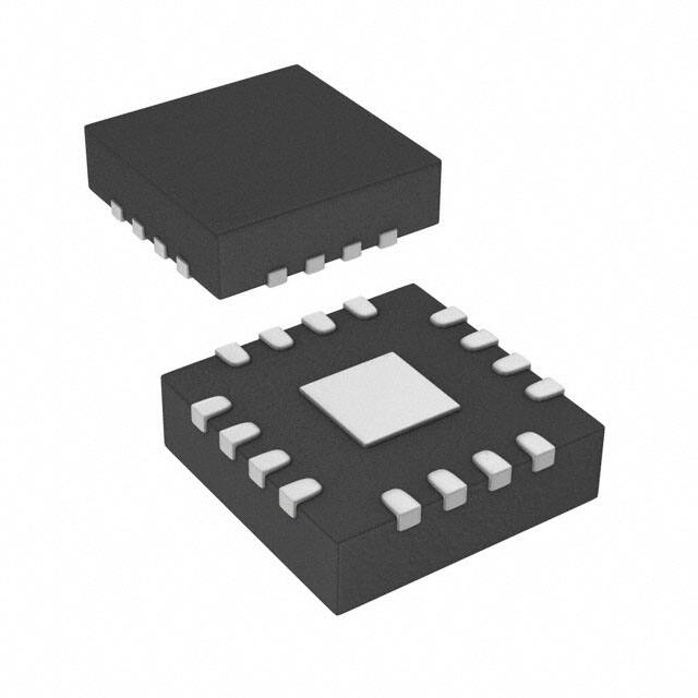


 工商网监
湘ICP备2023018690号
工商网监
湘ICP备2023018690号
