PIC16F631/677/685/687/689/690
20-Pin Flash-Based, 8-Bit CMOS Microcontrollers
High-Performance RISC CPU
Low-Power Features
• Only 35 Instructions to Learn:
- All single-cycle instructions except branches
• Operating Speed:
- DC – 20 MHz oscillator/clock input
- DC – 200 ns instruction cycle
• Interrupt Capability
• 8-Level Deep Hardware Stack
• Direct, Indirect and Relative Addressing modes
• Standby Current:
- 50 nA @ 2.0V, typical
• Operating Current:
- 11 A @ 32 kHz, 2.0V, typical
- 220 A @ 4 MHz, 2.0V, typical
• Watchdog Timer Current:
- 40 years
• Enhanced USART Module:
- Supports RS-485, RS-232 and LIN 2.0
- Auto-Baud Detect
- Auto-wake-up on Start bit
2005-2015 Microchip Technology Inc.
• 17 I/O Pins and 1 Input-Only Pin:
- High current source/sink for direct LED drive
- Interrupt-on-Change pin
- Individually programmable weak pull-ups
- Ultra Low-Power Wake-up (ULPWU)
• Analog Comparator Module with:
- Two analog comparators
- Programmable on-chip voltage reference
(CVREF) module (% of VDD)
- Comparator inputs and outputs externally
accessible
- SR Latch mode
- Timer 1 Gate Sync Latch
- Fixed 0.6V VREF
• A/D Converter:
- 10-bit resolution and 12 channels
• Timer0: 8-Bit Timer/Counter with 8-Bit
Programmable Prescaler
• Enhanced Timer1:
- 16-bit timer/counter with prescaler
- External Timer1 Gate (count enable)
- Option to use OSC1 and OSC2 in LP mode
as Timer1 oscillator if INTOSC mode
selected
• Timer2: 8-Bit Timer/Counter with 8-Bit Period
Register, Prescaler and Postscaler
• Enhanced Capture, Compare, PWM+ Module:
- 16-bit Capture, max resolution 12.5 ns
- Compare, max resolution 200 ns
- 10-bit PWM with 1, 2 or 4 output channels,
programmable “dead time”, max frequency
20 kHz
- PWM output steering control
• Synchronous Serial Port (SSP):
- SPI mode (Master and Slave)
• I2C™ (Master/Slave modes):
- I2C™ address mask
• In-Circuit Serial ProgrammingTM (ICSPTM) via Two
Pins
DS40001262F-page 1
�PIC16F631/677/685/687/689/690
Program
Memory
Data Memory
Flash
(words)
SRAM EEPROM
(bytes) (bytes)
Device
I/O
PIC16F631
PIC16F677
PIC16F685
PIC16F687
PIC16F689
PIC16F690
1024
2048
4096
2048
4096
4096
64
128
256
128
256
256
128
256
256
256
256
256
10-bit A/D
Comparators
(ch)
18
18
18
18
18
18
—
12
12
12
12
12
2
2
2
2
2
2
Timers
8/16-bit
SSP ECCP+ EUSART
1/1
1/1
2/1
1/1
1/1
2/1
No
Yes
No
Yes
Yes
Yes
No
No
Yes
No
No
Yes
No
No
No
Yes
Yes
Yes
PIC16F631 Pin Diagram
VDD
RA5/T1CKI/OSC1/CLKIN
RA4/T1G/OSC2/CLKOUT
RA3/MCLR/VPP
RC5
RC4/C2OUT
RC3/C12IN3RC6
RC7
RB7
TABLE 1:
1
2
3
4
5
6
7
8
9
10
PIC16F631
20-pin PDIP, SOIC, SSOP
20
19
18
17
16
15
14
13
12
11
VSS
RA0/C1IN+/ICSPDAT/ULPWU
RA1/C12IN0-/ICSPCLK
RA2/T0CKI/INT/C1OUT
RC0/C2IN+
RC1/C12IN1RC2/C12IN2RB4
RB5
RB6
PIC16F631 PIN SUMMARY
I/O
Pin
Analog
Comparators
Timers
Interrupt
Pull-up
Basic
RA0
19
AN0/ULPWU
C1IN+
—
IOC
Y
ICSPDAT
RA1
18
AN1
C12IN0-
—
IOC
Y
ICSPCLK
RA2
17
—
C1OUT
T0CKI
IOC/INT
Y
—
MCLR/VPP
RA3
4
—
—
—
IOC
Y(1)
RA4
3
—
—
T1G
IOC
Y
OSC2/CLKOUT
RA5
2
—
—
T1CKI
IOC
Y
OSC1/CLKIN
RB4
13
—
—
—
IOC
Y
—
RB5
12
—
—
—
IOC
Y
—
RB6
11
—
—
—
IOC
Y
—
RB7
10
—
—
—
IOC
Y
—
RC0
16
AN4
C2IN+
—
—
—
—
RC1
15
AN5
C12IN1-
—
—
—
—
RC2
14
AN6
C12IN2-
—
—
—
—
RC3
7
AN7
C12IN3-
—
—
—
—
RC4
6
—
C2OUT
—
—
—
—
RC5
5
—
—
—
—
—
—
RC6
8
—
—
—
—
—
—
RC7
9
—
—
—
—
—
—
—
1
—
—
—
—
—
VDD
—
20
—
—
—
—
—
VSS
Note 1:
Pull-up enabled only with external MCLR configuration.
DS40001262F-page 2
2005-2015 Microchip Technology Inc.
�PIC16F631/677/685/687/689/690
PIC16F677 Pin Diagram
VDD
RA5/T1CKI/OSC1/CLKIN
RA4/AN3/T1G/OSC2/CLKOUT
RA3/MCLR/VPP
RC5
RC4/C2OUT
RC3/AN7C12IN3RC6/AN8/SS
RC7/AN9/SDO
RB7
TABLE 2:
I/O
1
2
3
4
5
6
7
8
9
10
PIC16F677
20-pin PDIP, SOIC, SSOP
20
19
18
17
16
15
14
13
12
11
VSS
RA0/AN0/C1IN+/ICSPDAT/ULPWU
RA1/AN1/C12IN0-/VREF/ICSPCLK
RA2/AN2/T0CKI/INT/C1OUT
RC0/AN4/C2IN+
RC1/AN5/C12IN1RC2/AN6/C12IN2RB4/AN10/SDI/SDA
RB5/AN11
RB6/SCK/SCL
PIC16F631 PIN SUMMARY
Pin
Analog
Comparators
Timers
Interrupt
Pull-up
Basic
RA0
19
AN0/ULPWU
C1IN+
—
IOC
Y
ICSPDAT
RA1
18
AN1
C12IN0-
—
IOC
Y
ICSPCLK
RA2
17
—
C1OUT
T0CKI
IOC/INT
Y
—
RA3
4
—
—
—
IOC
Y(1)
MCLR/VPP
RA4
3
—
—
T1G
IOC
Y
OSC2/CLKOUT
RA5
2
—
—
T1CKI
IOC
Y
OSC1/CLKIN
RB4
13
—
—
—
IOC
Y
—
RB5
12
—
—
—
IOC
Y
—
RB6
11
—
—
—
IOC
Y
—
RB7
10
—
—
—
IOC
Y
—
RC0
16
AN4
C2IN+
—
—
—
—
RC1
15
AN5
C12IN1-
—
—
—
—
RC2
14
AN6
C12IN2-
—
—
—
—
RC3
7
AN7
C12IN3-
—
—
—
—
RC4
6
—
C2OUT
—
—
—
—
RC5
5
—
—
—
—
—
—
RC6
8
—
—
—
—
—
—
RC7
9
—
—
—
—
—
—
—
1
—
—
—
—
—
VDD
—
20
—
—
—
—
—
VSS
Note 1:
Pull-up enabled only with external MCLR configuration.
2005-2015 Microchip Technology Inc.
DS40001262F-page 3
�PIC16F631/677/685/687/689/690
PIC16F685 Pin Diagram
VDD
RA5/T1CKI/OSC1/CLKIN
RA4/AN3/T1G/OSC2/CLKOUT
RA3/MCLR/VPP
RC5/CCP1/P1A
RC4/C2OUT/P1B
RC3/AN7/C12IN3-/P1C
RC6/AN8
RC7/AN9
RB7
TABLE 3:
1
2
3
4
5
6
7
8
9
10
PIC16F685
20-pin PDIP, SOIC, SSOP
20
19
18
17
16
15
14
13
12
11
VSS
RA0/AN0/C1IN+/ICSPDAT/ULPWU
RA1/AN1/C12IN0-/VREF/ICSPCLK
RA2/AN2/T0CKI/INT/C1OUT
RC0/AN4/C2IN+
RC1/AN5/C12IN1RC2/AN6/C12IN2-/P1D
RB4/AN10
RB5/AN11
RB6
PIC16F685 PIN SUMMARY
I/O
Pin
Analog
Comparators
Timers
ECCP
Interrupt
Pull-up
Basic
RA0
19
AN0/ULPWU
C1IN+
—
—
IOC
Y
ICSPDAT
RA1
18
AN1/VREF
C12IN0-
—
—
IOC
Y
ICSPCLK
RA2
17
AN2
C1OUT
T0CKI
—
IOC/INT
Y
—
RA3
—
(1)
4
—
—
—
IOC
Y
RA4
3
AN3
RA5
2
—
—
T1G
—
IOC
Y
OSC2/CLKOUT
—
T1CKI
—
IOC
Y
OSC1/CLKIN
RB4
13
AN10
—
—
—
IOC
Y
—
RB5
12
AN11
—
—
—
IOC
Y
—
MCLR/VPP
RB6
11
—
—
—
—
IOC
Y
—
RB7
10
—
—
—
—
IOC
Y
—
RC0
16
AN4
C2IN+
—
—
—
—
—
RC1
15
AN5
C12IN1-
—
—
—
—
—
RC2
14
AN6
C12IN2-
—
P1D
—
—
—
RC3
7
AN7
C12IN3-
—
P1C
—
—
—
RC4
6
—
C2OUT
—
P1B
—
—
—
RC5
5
—
—
—
CCP1/P1A
—
—
—
RC6
8
AN8
—
—
—
—
—
—
RC7
9
AN9
—
—
—
—
—
—
—
1
—
—
—
—
—
—
VDD
—
20
—
—
—
—
—
—
VSS
Note 1:
Pull-up activated only with external MCLR configuration.
DS40001262F-page 4
2005-2015 Microchip Technology Inc.
�PIC16F631/677/685/687/689/690
PIC16F687/689 Pin Diagram
VDD
RA5/T1CKI/OSC1/CLKIN
RA4/AN3/T1G/OSC2/CLKOUT
RA3/MCLR/VPP
RC5
RC4/C2OUT
RC3/AN7/C12IN3RC6/AN8/SS
RC7/AN9/SDO
RB7/TX/CK
TABLE 4:
1
2
3
4
5
6
7
8
9
10
PIC16F687/689
20-pin PDIP, SOIC, SSOP
20
19
18
17
16
15
14
13
12
11
VSS
RA0/AN0/C1IN+/ICSPDAT/ULPWU
RA1/AN1/C12IN0-/VREF/ICSPCLK
RA2/AN2/T0CKI/INT/C1OUT
RC0/AN4/C2IN+
RC1/AN5/C12IN1RC2/AN6/C12IN2RB4/AN10/SDI/SDA
RB5/AN11/RX/DT
RB6/SCK/SCL
PIC16F687/689 PIN SUMMARY
I/O
Pin
Analog
Comparators
Timers
EUSART
SSP
RA0
19
AN0/ULPWU
C1IN+
—
—
—
RA1
18
AN1/VREF
C12IN0-
—
—
RA2
17
AN2
C1OUT
T0CKI
—
RA3
4
—
—
—
RA4
3
AN3
—
Interrupt Pull-up
Basic
IOC
Y
ICSPDAT
—
IOC
Y
ICSPCLK
—
IOC/INT
Y
—
—
IOC
Y(1)
MCLR/VPP
T1G
—
—
IOC
Y
OSC2/CLKOUT
RA5
2
—
—
T1CKI
—
—
IOC
Y
OSC1/CLKIN
RB4
13
AN10
—
—
—
SDI/SDA
IOC
Y
—
RB5
12
AN11
—
—
RX/DT
—
IOC
Y
—
RB6
11
—
—
—
—
SCL/SCK
IOC
Y
—
RB7
10
—
—
—
TX/CK
—
IOC
Y
—
RC0
16
AN4
C2IN+
—
—
—
—
—
—
RC1
15
AN5
C12IN1-
—
—
—
—
—
—
RC2
14
AN6
C12IN2-
—
—
—
—
—
—
RC3
7
AN7
C12IN3-
—
—
—
—
—
—
RC4
6
—
C2OUT
—
—
—
—
—
—
RC5
5
—
—
—
—
—
—
—
—
RC6
8
AN8
—
—
—
SS
—
—
—
RC7
9
AN9
—
—
—
SDO
—
—
—
—
1
—
—
—
—
—
—
—
VDD
—
20
—
—
—
—
—
—
—
VSS
Note 1: Pull-up activated only with external MCLR configuration.
2005-2015 Microchip Technology Inc.
DS40001262F-page 5
�PIC16F631/677/685/687/689/690
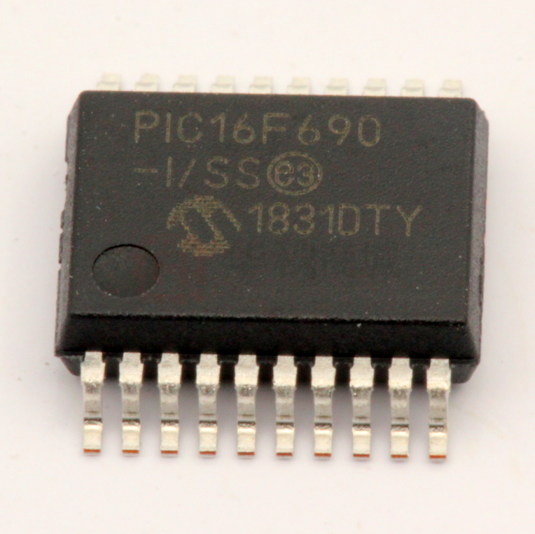
PIC16F690 Pin Diagram (PDIP, SOIC, SSOP)
VDD
RA5/T1CKI/OSC1/CLKIN
RA4/AN3/T1G/OSC2/CLKOUT
RA3/MCLR/VPP
RC5/CCP1/P1A
RC4/C2OUT/P1B
RC3/AN7/C12IN3-/P1C
RC6/AN8/SS
RC7/AN9/SDO
RB7/TX/CK
TABLE 5:
I/O
1
2
3
4
5
6
7
8
9
10
PIC16F690
20-pin PDIP, SOIC, SSOP
20
19
18
17
16
15
14
13
12
11
VSS
RA0/AN0/C1IN+/ICSPDAT/ULPWU
RA1/AN1/C12IN0-/VREF/ICSPCLK
RA2/AN2/T0CKI/INT/C1OUT
RC0/AN4/C2IN+
RC1/AN5/C12IN1RC2/AN6/C12IN2-/P1D
RB4/AN10/SDI/SDA
RB5/AN11/RX/DT
RB6/SCK/SCL
PIC16F690 PIN SUMMARY
Pin
Analog
Comparators Timers
ECCP
EUSART
SSP
Interrupt
Pull-up
Basic
RA0
19
AN0/ULPWU
C1IN+
—
—
—
—
IOC
Y
ICSPDAT
RA1
18
AN1/VREF
C12IN0-
—
—
—
—
IOC
Y
ICSPCLK
RA2
17
AN2
C1OUT
T0CKI
—
—
—
IOC/INT
Y
RA3
4
—
—
—
—
—
—
IOC
Y(1)
MCLR/VPP
RA4
3
AN3
—
T1G
—
—
—
IOC
Y
OSC2/CLKOUT
RA5
2
—
—
T1CKI
—
—
—
IOC
Y
OSC1/CLKIN
RB4
13
AN10
—
—
—
—
SDI/SDA
IOC
Y
—
RB5
12
AN11
—
—
—
RX/DT
—
IOC
Y
—
RB6
11
—
—
—
—
SCL/SCK
IOC
Y
—
RB7
10
—
—
—
—
—
IOC
Y
—
TX/CK
RC0
16
AN4
C2IN+
—
—
—
—
—
—
—
RC1
15
AN5
C12IN1-
—
—
—
—
—
—
—
RC2
14
AN6
C12IN2-
—
P1D
—
—
—
—
—
RC3
7
AN7
C12IN3-
—
P1C
—
—
—
—
—
RC4
6
—
C2OUT
—
P1B
—
—
—
—
—
RC5
5
—
—
—
CCP1/P1A
—
—
—
—
—
RC6
8
AN8
—
—
—
—
SS
—
—
—
RC7
9
AN9
—
—
—
—
SDO
—
—
—
—
1
—
—
—
—
—
—
—
—
VDD
—
20
—
—
—
—
—
—
—
—
VSS
Note 1: Pull-up activated only with external MCLR configuration.
DS40001262F-page 6
2005-2015 Microchip Technology Inc.
�PIC16F631/677/685/687/689/690
PIC16F631/677/685/687/689/690 Pin Diagram (QFN)
RA3/MCLR/VPP
1
(1)
2
RC5/CCP1/P1A
RA4/AN3/T1G/OSC2/CLKOUT
RA5/T1CKI/OSC1/CLKIN
VDD
VSS
RA0/AN0/C1IN+/ICSPDAT/ULPWU
20
19
18
17
16
20-pin QFN
PIC16F631/677/
685/687/689/690
15
RA1/AN1/C12IN0-/VREF/ICSPCLK
14
RA2/AN2/T0CKI/INT/C1OUT
13
RC0/AN4/C2IN+
11
RC2/AN6/C12IN2-/P1D(1)
RB4/AN10/SDI/SDA(2)
RB7/TX/CK
(3)
6
RC7/AN9/SDO(2)
Note 1:
9
5
RC6/AN8/SS
10
RC1/AN5/C12IN1-
RB5/AN11/RX/DT(3)
12
7
4
(2)
8
3
RC3/AN7/C12IN3-/P1C(1)
RC4/C2OUT/P1B
RB6/SCK/SCL(2)
(1)
CCP1/P1A, P1B, P1C and P1D are available on PIC16F685/PIC16F690 only.
2:
SS, SDO, SDI/SDA and SCL/SCK are available on PIC16F677/PIC16F687/PIC16F689/PIC16F690 only.
3:
RX/DT and TX/CK are available on PIC16F687/PIC16F689/PIC16F690 only.
2005-2015 Microchip Technology Inc.
DS40001262F-page 7
�PIC16F631/677/685/687/689/690
Table of Contents
1.0 Device Overview .......................................................................................................................................................................... 9
2.0 Memory Organization ................................................................................................................................................................. 24
3.0 Oscillator Module (With Fail-Safe Clock Monitor)....................................................................................................................... 45
4.0 I/O Ports ..................................................................................................................................................................................... 57
5.0 Timer0 Module ........................................................................................................................................................................... 79
6.0 Timer1 Module with Gate Control............................................................................................................................................... 82
7.0 Timer2 Module ........................................................................................................................................................................... 89
8.0 Comparator Module.................................................................................................................................................................... 91
9.0 Analog-to-Digital Converter (ADC) Module .............................................................................................................................. 105
10.0 Data EEPROM and Flash Program Memory Control ............................................................................................................... 117
11.0 Enhanced Capture/Compare/PWM Module ............................................................................................................................. 125
12.0 Enhanced Universal Synchronous Asynchronous Receiver Transmitter (EUSART) ............................................................... 148
13.0 SSP Module Overview ............................................................................................................................................................. 175
14.0 Special Features of the CPU .................................................................................................................................................... 193
15.0 Instruction Set Summary .......................................................................................................................................................... 212
16.0 Development Support............................................................................................................................................................... 221
17.0 Electrical Specifications............................................................................................................................................................ 225
18.0 DC and AC Characteristics Graphs and Tables ....................................................................................................................... 258
19.0 Packaging Information.............................................................................................................................................................. 285
The Microchip Web Site ..................................................................................................................................................................... 295
Customer Change Notification Service .............................................................................................................................................. 295
Customer Support .............................................................................................................................................................................. 295
Product Identification System............................................................................................................................................................. 296
TO OUR VALUED CUSTOMERS
It is our intention to provide our valued customers with the best documentation possible to ensure successful use of your Microchip
products. To this end, we will continue to improve our publications to better suit your needs. Our publications will be refined and
enhanced as new volumes and updates are introduced.
If you have any questions or comments regarding this publication, please contact the Marketing Communications Department via Email at docerrors@microchip.com. We welcome your feedback.
Most Current Data Sheet
To obtain the most up-to-date version of this data sheet, please register at our Worldwide Web site at:
http://www.microchip.com
You can determine the version of a data sheet by examining its literature number found on the bottom outside corner of any page.
The last character of the literature number is the version number, (e.g., DS30000000A is version A of document DS30000000).
Errata
An errata sheet, describing minor operational differences from the data sheet and recommended workarounds, may exist for current
devices. As device/documentation issues become known to us, we will publish an errata sheet. The errata will specify the revision of
silicon and revision of document to which it applies.
To determine if an errata sheet exists for a particular device, please check with one of the following:
• Microchip’s Worldwide Web site; http://www.microchip.com
• Your local Microchip sales office (see last page)
When contacting a sales office, please specify which device, revision of silicon and data sheet (include literature number) you are
using.
Customer Notification System
Register on our web site at www.microchip.com to receive the most current information on all of our products.
DS40001262F-page 8
2005-2015 Microchip Technology Inc.
�PIC16F631/677/685/687/689/690
1.0
DEVICE OVERVIEW
Block Diagrams and pinout descriptions of the devices
are as follows:
The PIC16F631/677/685/687/689/690 devices are
covered by this data sheet. They are available in 20-pin
PDIP, SOIC, TSSOP and QFN packages.
FIGURE 1-1:
•
•
•
•
•
PIC16F631 (Figure 1-1, Table 1-1)
PIC16F677 (Figure 1-2, Table 1-2)
PIC16F685 (Figure 1-3, Table 1-3)
PIC16F687/PIC16F689 (Figure 1-4, Table 1-4)
PIC16F690 (Figure 1-5, Table 1-5)
PIC16F631 BLOCK DIAGRAM
INT
Configuration
13
8
Data Bus
PORTA
Program Counter
RA0
RA1
RA2
RA3
RA4
RA5
Flash
1K x 14
Program
RAM
64 bytes
File
Registers
8-Level Stack (13-bit)
Memory
Program 14
Bus
RAM Addr
9
PORTB
Addr MUX
Instruction Reg
7
Direct Addr
8
RB4
RB5
RB6
RB7
Indirect
Addr
FSR Reg
STATUS Reg
8
PORTC
3
Power-up
Timer
Instruction
Decode and
Control
OSC1/CLKI
Oscillator
Start-up Timer
ALU
Power-on
Reset
OSC2/CLKO
Timing
Generation
RC0
RC1
RC2
RC3
RC4
RC5
RC6
RC7
MUX
8
Watchdog
Timer
W Reg
Brown-out
Reset
Internal
Oscillator
Block
MCLR VDD
ULPWU
Ultra Low-Power
Wake-up
T0CKI
VSS
T1G
T1CKI
C1IN- C1IN+ C1OUT C2IN- C2IN+ C2OUT
EEDAT
128 Bytes
Data
EEPROM
Timer0
Timer1
EEADR
2
Analog Comparators
and Reference
8
2005-2015 Microchip Technology Inc.
DS40001262F-page 9
�PIC16F631/677/685/687/689/690
FIGURE 1-2:
PIC16F677 BLOCK DIAGRAM
INT
Configuration
13
8
Data Bus
PORTA
Program Counter
Flash
RA0
RA1
RA2
RA3
RA4
RA5
2K x 14
Program
RAM
128 bytes
File
Registers
8-Level Stack (13-bit)
Memory
Program 14
Bus
RAM Addr
9
PORTB
Addr MUX
Instruction Reg
7
Direct Addr
8
Indirect
Addr
RB4
RB5
RB6
RB7
FSR Reg
STATUS Reg
8
PORTC
3
Power-up
Timer
Instruction
Decode and
Control
Oscillator
Start-up Timer
OSC1/CLKI
ALU
Power-on
Reset
OSC2/CLKO
Timing
Generation
RC0
RC1
RC2
RC3
RC4
RC5
RC6
RC7
MUX
8
Watchdog
Timer
W Reg
Brown-out
Reset
Internal
Oscillator
Block
MCLR VDD
ULPWU
T0CKI
Ultra Low-Power
Wake-up
Timer0
VSS
T1G
SDI/ SCK/
SDO SDA SCL SS
T1CKI
Synchronous
Serial Port
Timer1
AN8 AN9 AN10 AN11
EEDAT
Analog-to-Digital Converter
2
Analog Comparators
and Reference
8
256 Bytes
Data
EEPROM
EEADR
VREF AN0 AN1 AN2 AN3 AN4 AN5 AN6 AN7 C1IN- C1IN+ C1OUT C2IN- C2IN+ C2OUT
DS40001262F-page 10
2005-2015 Microchip Technology Inc.
�PIC16F631/677/685/687/689/690
FIGURE 1-3:
PIC16F685 BLOCK DIAGRAM
INT
Configuration
13
8
Data Bus
PORTA
Program Counter
Flash
RA0
RA1
RA2
RA3
RA4
RA5
4K x 14
Program
RAM
256 bytes
File
Registers
8-Level Stack (13-bit)
Memory
Program 14
Bus
RAM Addr
9
PORTB
Addr MUX
Instruction Reg
7
Direct Addr
8
Indirect
Addr
RB4
RB5
RB6
RB7
FSR Reg
STATUS Reg
8
PORTC
3
Power-up
Timer
Instruction
Decode and
Control
Oscillator
Start-up Timer
OSC1/CLKI
ALU
Power-on
Reset
OSC2/CLKO
Timing
Generation
RC0
RC1
RC2
RC3
RC4
RC5
RC6
RC7
MUX
8
Watchdog
Timer
W Reg
Brown-out
Reset
Internal
Oscillator
Block
MCLR VDD
ULPWU
T0CKI
Ultra Low-Power
Wake-up
Timer0
VSS
T1G
CCP1/
P1A P1B P1C P1D
T1CKI
Timer1
Timer2
ECCP+
AN8 AN9 AN10 AN11
EEDAT
Analog-to-Digital Converter
2
Analog Comparators
and Reference
8
256 Bytes
Data
EEPROM
EEADR
VREF AN0 AN1 AN2 AN3 AN4 AN5 AN6 AN7 C1IN- C1IN+ C1OUT C2IN- C2IN+ C2OUT
2005-2015 Microchip Technology Inc.
DS40001262F-page 11
�PIC16F631/677/685/687/689/690
FIGURE 1-4:
PIC16F687/PIC16F689 BLOCK DIAGRAM
INT
Configuration
13
8
Data Bus
PORTA
Program Counter
Flash
RA0
RA1
RA2
RA3
RA4
RA5
2K(1)/4K x 14
Program
RAM
128(1)/256 bytes
File
Registers
8-Level Stack (13-bit)
Memory
Program 14
Bus
RAM Addr
9
PORTB
Addr MUX
Instruction Reg
Indirect
Addr
7
Direct Addr
8
RB4
RB5
RB6
RB7
FSR Reg
STATUS Reg
8
PORTC
3
Power-up
Timer
Instruction
Decode and
Control
Oscillator
Start-up Timer
OSC1/CLKI
ALU
Power-on
Reset
Timing
Generation
OSC2/CLKO
RC0
RC1
RC2
RC3
RC4
RC5
RC6
RC7
MUX
8
Watchdog
Timer
W Reg
Brown-out
Reset
Internal
Oscillator
Block
MCLR VDD
ULPWU
T0CKI
Ultra Low-Power
Wake-up
Timer0
VSS
T1G
T1CKI
Timer1
TX/CK
SDI/ SCK/
SDO SDA SCL SS
RX/DT
Synchronous
Serial Port
EUSART
AN8 AN9 AN10 AN11
EEDAT
Analog-to-Digital Converter
2
Analog Comparators
and Reference
8
256 Bytes
Data
EEPROM
EEADR
VREF AN0 AN1 AN2 AN3 AN4 AN5 AN6 AN7 C1IN- C1IN+ C1OUT C2IN- C2IN+ C2OUT
Note
1:
PIC16F687 only.
DS40001262F-page 12
2005-2015 Microchip Technology Inc.
�PIC16F631/677/685/687/689/690
FIGURE 1-5:
PIC16F690 BLOCK DIAGRAM
INT
Configuration
13
8
Data Bus
PORTA
Program Counter
Flash
RA0
RA1
RA2
RA3
RA4
RA5
4k x 14
Program
RAM
256 bytes
File
Registers
8-Level Stack (13-bit)
Memory
Program 14
Bus
RAM Addr
9
PORTB
Addr MUX
Instruction Reg
Direct Addr
7
8
Indirect
Addr
RB4
RB5
RB6
RB7
FSR Reg
STATUS Reg
8
PORTC
3
Power-up
Timer
Instruction
Decode and
Control
Oscillator
Start-up Timer
OSC1/CLKI
OSC2/CLKO
Power-on
Reset
Timing
Generation
RC0
RC1
RC2
RC3
RC4
RC5
RC6
RC7
MUX
ALU
8
Watchdog
Timer
W Reg
Brown-out
Reset
Internal
Oscillator
Block
MCLR VDD
ULPWU
T0CKI
Ultra Low-Power
Wake-up
Timer0
T1G
VSS
TX/CK RX/DT
T1CKI
Timer1
Timer2
CCP1/
P1A
EUSART
P1B P1C P1D
ECCP+
SDI/ SCK/
SDO SDA SCL SS
Synchronous
Serial Port
AN8 AN9 AN10 AN11
EEDAT
Analog-to-Digital Converter
2
Analog Comparators
and Reference
8
256 Bytes
Data
EEPROM
EEADR
VREF AN0 AN1 AN2 AN3 AN4 AN5 AN6 AN7 C1IN- C1IN+ C1OUT C2IN- C2IN+ C2OUT
2005-2015 Microchip Technology Inc.
DS40001262F-page 13
�PIC16F631/677/685/687/689/690
TABLE 1-1:
PINOUT DESCRIPTION – PIC16F631
Name
RA0/C1IN+/ICSPDAT/ULPWU
RA1/C12IN0-/ICSPCLK
RA2/T0CKI/INT/C1OUT
RA3/MCLR/VPP
RA4/T1G/OSC2/CLKOUT
RA5/T1CKI/OSC1/CLKIN
Function
Input
Type
RA0
TTL
C1IN+
AN
ICSPDAT
ST
ULPWU
AN
RA1
TTL
Output
Type
Description
CMOS General purpose I/O. Individually controlled interrupt-on-change.
Individually enabled pull-up.
—
Comparator C1 non-inverting input.
CMOS ICSP™ Data I/O.
—
Ultra Low-Power Wake-up input.
CMOS General purpose I/O. Individually controlled interrupt-on-change.
Individually enabled pull-up.
C12IN0-
AN
—
Comparator C1 or C2 inverting input.
ICSPCLK
ST
—
ICSP™ clock.
RA2
ST
T0CKI
ST
—
Timer0 clock input.
INT
ST
—
External interrupt pin.
C1OUT
—
RA3
TTL
—
General purpose input. Individually controlled interrupt-onchange.
MCLR
ST
—
Master Clear with internal pull-up.
—
Programming voltage.
CMOS General purpose I/O. Individually controlled interrupt-on-change.
Individually enabled pull-up.
CMOS Comparator C1 output.
VPP
HV
RA4
TTL
T1G
ST
—
Timer1 gate input.
OSC2
—
XTAL
Crystal/Resonator.
CLKOUT
—
RA5
TTL
CMOS General purpose I/O. Individually controlled interrupt-on-change.
Individually enabled pull-up.
CMOS FOSC/4 output.
CMOS General purpose I/O. Individually controlled interrupt-on-change.
Individually enabled pull-up.
T1CKI
ST
—
Timer1 clock input.
OSC1
XTAL
—
Crystal/Resonator.
—
External clock input/RC oscillator connection.
CLKIN
ST
RB4
RB4
TTL
CMOS General purpose I/O. Individually controlled interrupt-on-change.
Individually enabled pull-up.
RB5
RB5
TTL
CMOS General purpose I/O. Individually controlled interrupt-on-change.
Individually enabled pull-up.
RB6
RB6
TTL
CMOS General purpose I/O. Individually controlled interrupt-on-change.
Individually enabled pull-up.
RB7
RB7
TTL
CMOS General purpose I/O. Individually controlled interrupt-on-change.
Individually enabled pull-up.
CMOS General purpose I/O.
RC0/C2IN+
RC1/C12IN1RC2/C12IN2RC3/C12IN3RC4/C2OUT
RC5
Legend:
RC0
ST
C2IN+
AN
RC1
ST
C12IN1-
AN
RC2
ST
C12IN2-
AN
RC3
ST
C12IN3-
AN
RC4
ST
Comparator C2 non-inverting input.
—
Comparator C1 or C2 inverting input.
CMOS General purpose I/O.
—
Comparator C1 or C2 inverting input.
CMOS General purpose I/O.
—
Comparator C1 or C2 inverting input.
CMOS General purpose I/O.
C2OUT
—
CMOS Comparator C2 output.
RC5
ST
CMOS General purpose I/O.
AN = Analog input or output
TTL = TTL compatible input
HV = High Voltage
DS40001262F-page 14
—
CMOS General purpose I/O.
CMOS=CMOS compatible input or output
ST=
Schmitt Trigger input with CMOS levels
XTAL= Crystal
2005-2015 Microchip Technology Inc.
�PIC16F631/677/685/687/689/690
TABLE 1-1:
PINOUT DESCRIPTION – PIC16F631 (CONTINUED)
Function
Input
Type
RC6
RC6
ST
CMOS General purpose I/O.
RC7
RC7
ST
CMOS General purpose I/O.
VSS
VSS
Power
—
Ground reference.
VDD
VDD
Power
—
Positive supply.
Name
Legend:
AN = Analog input or output
TTL = TTL compatible input
HV = High Voltage
2005-2015 Microchip Technology Inc.
Output
Type
Description
CMOS=CMOS compatible input or output
ST=
Schmitt Trigger input with CMOS levels
XTAL= Crystal
DS40001262F-page 15
�PIC16F631/677/685/687/689/690
TABLE 1-2:
PINOUT DESCRIPTION – PIC16F677
Name
RA0/AN0/C1IN+/ICSPDAT/
ULPWU
RA1/AN1/C12IN0-/VREF/
ICSPCLK
RA2/AN2/T0CKI/INT/C1OUT
RA3/MCLR/VPP
RA4/AN3/T1G/OSC2/CLKOUT
RA5/T1CKI/OSC1/CLKIN
RB4/AN10/SDI/SDA
RB5/AN11
RB6/SCK/SCL
Legend:
Function
Input
Type
RA0
TTL
Description
CMOS General purpose I/O. Individually controlled interrupt-on-change.
Individually enabled pull-up.
AN0
AN
—
A/D Channel 0 input.
C1IN+
AN
—
Comparator C1 non-inverting input.
ICSPDAT
ST
ULPWU
AN
RA1
TTL
CMOS ICSP™ Data I/O.
—
Ultra Low-Power Wake-up input.
CMOS General purpose I/O. Individually controlled interrupt-on-change.
Individually enabled pull-up.
AN1
AN
—
A/D Channel 1 input.
C12IN0-
AN
—
Comparator C1 or C2 inverting input.
VREF
AN
—
External Voltage Reference for A/D.
ICSPCLK
ST
—
ICSP™ clock.
RA2
ST
AN2
AN
—
A/D Channel 2 input.
T0CKI
ST
—
Timer0 clock input.
INT
ST
—
External interrupt pin.
C1OUT
—
RA3
TTL
CMOS General purpose I/O. Individually controlled interrupt-on-change.
Individually enabled pull-up.
CMOS Comparator C1 output.
—
General purpose input. Individually controlled interrupt-onchange.
MCLR
ST
—
Master Clear with internal pull-up.
VPP
HV
—
Programming voltage.
RA4
TTL
AN3
AN
T1G
ST
—
Timer1 gate input.
OSC2
—
XTAL
Crystal/Resonator.
CLKOUT
—
RA5
TTL
CMOS General purpose I/O. Individually controlled interrupt-on-change.
Individually enabled pull-up.
—
A/D Channel 3 input.
CMOS FOSC/4 output.
CMOS General purpose I/O. Individually controlled interrupt-on-change.
Individually enabled pull-up.
T1CKI
ST
—
Timer1 clock input.
OSC1
XTAL
—
Crystal/Resonator.
—
External clock input/RC oscillator connection.
CLKIN
ST
RB4
TTL
AN10
AN
—
A/D Channel 10 input.
SDI
ST
—
SPI data input.
SDA
ST
OD
I2C™ data input/output.
RB5
TTL
CMOS General purpose I/O. Individually controlled interrupt-on-change.
Individually enabled pull-up.
CMOS General purpose I/O. Individually controlled interrupt-on-change.
Individually enabled pull-up.
AN11
AN
RB6
TTL
CMOS General purpose I/O. Individually controlled interrupt-on-change.
Individually enabled pull-up.
SCK
ST
CMOS SPI clock.
SCL
ST
AN = Analog input or output
TTL = TTL compatible input
HV = High Voltage
DS40001262F-page 16
Output
Type
—
OD
A/D Channel 11 input.
I2C™ clock.
CMOS=CMOS compatible input or output
ST=
Schmitt Trigger input with CMOS levels
XTAL= Crystal
2005-2015 Microchip Technology Inc.
�PIC16F631/677/685/687/689/690
TABLE 1-2:
PINOUT DESCRIPTION – PIC16F677 (CONTINUED)
Function
Input
Type
RB7
RB7
TTL
CMOS General purpose I/O. Individually controlled interrupt-on-change.
Individually enabled pull-up.
RC0/AN4/C2IN+
RC0
ST
CMOS General purpose I/O.
AN4
AN
C2IN+
AN
RC1
ST
Name
RC1/AN5/C12IN1-
RC2/AN6/C12IN2-
RC3/AN7/C12IN3-
RC4/C2OUT
Output
Type
Description
—
A/D Channel 4 input.
—
Comparator C2 non-inverting input.
CMOS General purpose I/O.
AN5
AN
—
A/D Channel 5 input.
C12IN1-
AN
—
Comparator C1 or C2 inverting input.
RC2
ST
AN6
AN
CMOS General purpose I/O.
—
A/D Channel 6 input.
C12IN2-
AN
—
Comparator C1 or C2 inverting input.
RC3
ST
CMOS General purpose I/O.
AN7
AN
—
A/D Channel 7 input.
C12IN3-
AN
—
Comparator C1 or C2 inverting input.
RC4
ST
CMOS General purpose I/O.
C2OUT
—
CMOS Comparator C2 output.
RC5
RC5
ST
CMOS General purpose I/O.
RC6/AN8/SS
RC6
ST
CMOS General purpose I/O.
AN8
AN
—
A/D Channel 8 input.
SS
ST
—
Slave Select input.
RC7/AN9/SDO
VSS
VDD
Legend:
RC7
ST
AN9
AN
SDO
—
VSS
Power
—
Ground reference.
VDD
Power
—
Positive supply.
AN = Analog input or output
TTL = TTL compatible input
HV = High Voltage
2005-2015 Microchip Technology Inc.
CMOS General purpose I/O.
—
A/D Channel 9 input.
CMOS SPI data output.
CMOS=CMOS compatible input or output
ST=
Schmitt Trigger input with CMOS levels
XTAL= Crystal
DS40001262F-page 17
�PIC16F631/677/685/687/689/690
TABLE 1-3:
PINOUT DESCRIPTION – PIC16F685
Name
RA0/AN0/C1IN+/ICSPDAT/
ULPWU
RA1/AN1/C12IN0-/VREF/ICSPCLK
RA2/AN2/T0CKI/INT/C1OUT
RA3/MCLR/VPP
RA4/AN3/T1G/OSC2/CLKOUT
RA5/T1CKI/OSC1/CLKIN
RB4/AN10
RB5/AN11
Function
Input
Type
RA0
TTL
Output
Type
Description
CMOS General purpose I/O. Individually controlled interrupt-onchange. Individually enabled pull-up.
AN0
AN
—
A/D Channel 0 input.
C1IN+
AN
—
Comparator C1 positive input.
ICSPDAT
TTL
ULPWU
AN
RA1
TTL
CMOS ICSP™ Data I/O.
—
Ultra Low-Power Wake-up input.
CMOS General purpose I/O. Individually controlled interrupt-onchange. Individually enabled pull-up.
AN1
AN
—
A/D Channel 1 input.
C12IN0-
AN
—
Comparator C1 or C2 negative input.
VREF
AN
—
External Voltage Reference for A/D.
ICSPCLK
ST
—
ICSP™ clock.
RA2
ST
AN2
AN
CMOS General purpose I/O. Individually controlled interrupt-onchange. Individually enabled pull-up.
—
A/D Channel 2 input.
T0CKI
ST
—
Timer0 clock input.
INT
ST
—
External interrupt pin.
C1OUT
—
RA3
TTL
CMOS Comparator C1 output.
—
General purpose input. Individually controlled interrupt-onchange.
MCLR
ST
—
Master Clear with internal pull-up.
VPP
HV
—
Programming voltage.
RA4
TTL
AN3
AN
T1G
ST
—
Timer1 gate input.
OSC2
—
XTAL
Crystal/Resonator.
CLKOUT
—
CMOS FOSC/4 output.
RA5
TTL
CMOS General purpose I/O. Individually controlled interrupt-onchange. Individually enabled pull-up.
—
A/D Channel 3 input.
CMOS General purpose I/O. Individually controlled interrupt-onchange. Individually enabled pull-up.
T1CKI
ST
—
Timer1 clock input.
OSC1
XTAL
—
Crystal/Resonator.
—
External clock input/RC oscillator connection.
CLKIN
ST
RB4
TTL
AN10
AN
RB5
TTL
CMOS General purpose I/O. Individually controlled interrupt-onchange. Individually enabled pull-up.
—
A/D Channel 10 input.
CMOS General purpose I/O. Individually controlled interrupt-onchange. Individually enabled pull-up.
AN11
AN
RB6
RB6
TTL
CMOS General purpose I/O. Individually controlled interrupt-onchange. Individually enabled pull-up.
RB7
RB7
TTL
CMOS General purpose I/O. Individually controlled interrupt-onchange. Individually enabled pull-up.
RC0/AN4/C2IN+
RC0
ST
CMOS General purpose I/O.
Legend:
A/D Channel 11 input.
AN4
AN
—
A/D Channel 4 input.
C2IN+
AN
—
Comparator C2 positive input.
AN = Analog input or output
TTL = TTL compatible input
HV = High Voltage
DS40001262F-page 18
—
CMOS=CMOS compatible input or output
ST=
Schmitt Trigger input with CMOS levels
XTAL= Crystal
2005-2015 Microchip Technology Inc.
�PIC16F631/677/685/687/689/690
TABLE 1-3:
PINOUT DESCRIPTION – PIC16F685 (CONTINUED)
Name
Function
Input
Type
RC1
ST
RC1/AN5/C12IN1-
Output
Type
Description
CMOS General purpose I/O.
AN5
AN
—
A/D Channel 5 input.
C12IN1-
AN
—
Comparator C1 or C2 negative input.
RC2/AN6/C12IN2-/P1D
RC2
ST
AN6
AN
C12IN2-
AN
P1D
—
CMOS PWM output.
RC3
ST
CMOS General purpose I/O.
AN7
AN
C12IN3-
AN
P1C
—
CMOS PWM output.
RC4
ST
CMOS General purpose I/O.
C2OUT
—
CMOS Comparator C2 output.
RC3/AN7/C12IN3-/P1C
RC4/C2OUT/P1B
RC5/CCP1/P1A
CMOS General purpose I/O.
—
A/D Channel 6 input.
—
Comparator C1 or C2 negative input.
—
A/D Channel 7 input.
—
Comparator C1 or C2 negative input.
P1B
—
CMOS PWM output.
RC5
ST
CMOS General purpose I/O.
CCP1
ST
CMOS Capture/Compare input.
P1A
ST
CMOS PWM output.
RC6
ST
CMOS General purpose I/O.
AN8
AN
RC7
ST
AN9
AN
—
A/D Channel 9 input.
VSS
VSS
Power
—
Ground reference.
VDD
VDD
Power
—
Positive supply.
RC6/AN8
RC7/AN9
Legend:
AN = Analog input or output
TTL = TTL compatible input
HV = High Voltage
2005-2015 Microchip Technology Inc.
—
A/D Channel 8 input.
CMOS General purpose I/O.
CMOS=CMOS compatible input or output
ST=
Schmitt Trigger input with CMOS levels
XTAL= Crystal
DS40001262F-page 19
�PIC16F631/677/685/687/689/690
TABLE 1-4:
PINOUT DESCRIPTION – PIC16F687/PIC16F689
Name
RA0/AN0/C1IN+/ICSPDAT/
ULPWU
RA1/AN1/C12IN0-/VREF/ICSPCLK
RA2/AN2/T0CKI/INT/C1OUT
RA3/MCLR/VPP
RA4/AN3/T1G/OSC2/CLKOUT
RA5/T1CKI/OSC1/CLKIN
RB4/AN10/SDI/SDA
RB5/AN11/RX/DT
Function
Input
Type
RA0
TTL
CMOS General purpose I/O. Individually controlled interrupt-onchange. Individually enabled pull-up.
AN0
AN
—
A/D Channel 0 input.
AN
—
Comparator C1 positive input.
ICSPDAT
TTL
ULPWU
AN
RA1
TTL
CMOS ICSP™ Data I/O.
—
Ultra Low-Power Wake-up input.
CMOS General purpose I/O. Individually controlled interrupt-onchange. Individually enabled pull-up.
AN1
AN
—
A/D Channel 1 input.
C12IN0-
AN
—
Comparator C1 or C2 negative input.
VREF
AN
—
External Voltage Reference for A/D.
ICSPCLK
ST
—
ICSP™ clock.
RA2
ST
AN2
AN
—
A/D Channel 2 input.
T0CKI
ST
—
Timer0 clock input.
INT
ST
—
External Interrupt.
C1OUT
—
RA3
TTL
CMOS General purpose I/O. Individually controlled interrupt-onchange. Individually enabled pull-up.
CMOS Comparator C1 output.
—
General purpose input. Individually controlled
interrupt-on-change.
MCLR
ST
—
Master Clear with internal pull-up.
VPP
HV
—
Programming voltage.
RA4
TTL
AN3
AN
T1G
ST
—
Timer1 gate input.
OSC2
—
XTAL
Crystal/Resonator.
CLKOUT
—
CMOS FOSC/4 output.
RA5
TTL
CMOS General purpose I/O. Individually controlled interrupt-onchange. Individually enabled pull-up.
—
A/D Channel 3 input.
CMOS General purpose I/O. Individually controlled interrupt-onchange. Individually enabled pull-up.
T1CKI
ST
—
Timer1 clock input.
OSC1
XTAL
—
Crystal/Resonator.
—
External clock input/RC oscillator connection.
CLKIN
ST
RB4
TTL
AN10
AN
—
A/D Channel 10 input.
SDI
ST
—
SPI data input.
SDA
ST
OD
I2C™ data input/output.
RB5
TTL
AN11
AN
—
A/D Channel 11 input.
RX
ST
—
EUSART asynchronous input.
AN = Analog input or output
TTL = TTL compatible input
HV = High Voltage
DS40001262F-page 20
Description
C1IN+
DT
Legend:
Output
Type
ST
CMOS General purpose I/O. Individually controlled interrupt-onchange. Individually enabled pull-up.
CMOS General purpose I/O. Individually controlled interrupt-onchange. Individually enabled pull-up.
CMOS EUSART synchronous data.
CMOS=CMOS compatible input or outputOD=
ST=
Schmitt Trigger input with CMOS levels
XTAL= Crystal
Open Drain
2005-2015 Microchip Technology Inc.
�PIC16F631/677/685/687/689/690
TABLE 1-4:
PINOUT DESCRIPTION – PIC16F687/PIC16F689 (CONTINUED)
Name
Function
Input
Type
RB6
TTL
CMOS General purpose I/O. Individually controlled interrupt-onchange. Individually enabled pull-up.
SCK
ST
CMOS SPI clock.
SCL
ST
RB7
TTL
TX
—
RB6/SCK/SCL
RB7/TX/CK
RC0/AN4/C2IN+
Output
Type
OD
Description
I2C™ clock.
CMOS General purpose I/O. Individually controlled interrupt-onchange. Individually enabled pull-up.
CMOS EUSART asynchronous output.
CK
ST
CMOS EUSART synchronous clock.
RC0
ST
CMOS General purpose I/O.
AN4
AN
—
A/D Channel 4 input.
C2IN+
AN
—
Comparator C2 positive input.
RC1/AN5/C12IN1-
RC1
ST
AN5
AN
—
A/D Channel 5 input.
C12IN1-
AN
—
Comparator C1 or C2 negative input.
RC2
ST
RC2/AN6/C12IN2-
CMOS General purpose I/O.
CMOS General purpose I/O.
AN6
AN
—
A/D Channel 6 input.
C12IN2-
AN
—
Comparator C1 or C2 negative input.
RC3/AN7/C12IN3-
RC3
ST
AN7
AN
C12IN3-
AN
RC4
ST
RC4/C2OUT
CMOS General purpose I/O.
—
A/D Channel 7 input.
—
Comparator C1 or C2 negative input.
CMOS General purpose I/O.
C2OUT
—
CMOS Comparator C2 output.
RC5
RC5
ST
CMOS General purpose I/O.
RC6/AN8/SS
RC6
ST
CMOS General purpose I/O.
AN8
AN
—
A/D Channel 8 input.
SS
ST
—
Slave Select input.
RC7
ST
RC7/AN9/SDO
CMOS General purpose I/O.
AN9
AN
SDO
—
VSS
VSS
Power
—
Ground reference.
VDD
VDD
Power
—
Positive supply.
Legend:
AN = Analog input or output
TTL = TTL compatible input
HV = High Voltage
2005-2015 Microchip Technology Inc.
—
A/D Channel 9 input.
CMOS SPI data output.
CMOS=CMOS compatible input or outputOD=
ST=
Schmitt Trigger input with CMOS levels
XTAL= Crystal
Open Drain
DS40001262F-page 21
�PIC16F631/677/685/687/689/690
TABLE 1-5:
PINOUT DESCRIPTION – PIC16F690
Name
RA0/AN0/C1IN+/ICSPDAT/
ULPWU
RA1/AN1/C12IN0-/VREF/ICSPCLK
RA2/AN2/T0CKI/INT/C1OUT
RA3/MCLR/VPP
RA4/AN3/T1G/OSC2/CLKOUT
RA5/T1CKI/OSC1/CLKIN
RB4/AN10/SDI/SDA
RB5/AN11/RX/DT
Function
Input
Type
RA0
TTL
CMOS General purpose I/O. Individually controlled interrupt-onchange. Individually enabled pull-up.
AN0
AN
—
A/D Channel 0 input.
AN
—
Comparator C1 positive input.
ICSPDAT
TTL
ULPWU
AN
RA1
TTL
CMOS ICSP™ Data I/O.
—
Ultra Low-Power Wake-up input.
CMOS General purpose I/O. Individually controlled interrupt-onchange. Individually enabled pull-up.
AN1
AN
—
A/D Channel 1 input.
C12IN0-
AN
—
Comparator C1 or C2 negative input.
VREF
AN
—
External Voltage Reference for A/D.
ICSPCLK
ST
—
ICSP™ clock.
RA2
ST
AN2
AN
—
A/D Channel 2 input.
T0CKI
ST
—
Timer0 clock input.
INT
ST
—
External interrupt.
C1OUT
—
RA3
TTL
CMOS General purpose I/O. Individually controlled interrupt-onchange. Individually enabled pull-up.
CMOS Comparator C1 output.
—
General purpose input. Individually controlled interrupt-onchange.
MCLR
ST
—
Master Clear with internal pull-up.
VPP
HV
—
Programming voltage.
RA4
TTL
AN3
AN
T1G
ST
—
Timer1 gate input.
OSC2
—
XTAL
Crystal/Resonator.
CLKOUT
—
CMOS FOSC/4 output.
RA5
TTL
CMOS General purpose I/O. Individually controlled interrupt-onchange. Individually enabled pull-up.
—
A/D Channel 3 input.
CMOS General purpose I/O. Individually controlled interrupt-onchange. Individually enabled pull-up.
T1CKI
ST
—
Timer1 clock input.
OSC1
XTAL
—
Crystal/Resonator.
—
External clock input/RC oscillator connection.
CLKIN
ST
RB4
TTL
AN10
AN
—
A/D Channel 10 input.
SDI
ST
—
SPI data input.
SDA
ST
OD
I2C™ data input/output.
RB5
TTL
AN11
AN
—
A/D Channel 11 input.
RX
ST
—
EUSART asynchronous input.
AN = Analog input or output
TTL = TTL compatible input
HV = High Voltage
DS40001262F-page 22
Description
C1IN+
DT
Legend:
Output
Type
ST
CMOS General purpose I/O. Individually controlled interrupt-onchange. Individually enabled pull-up.
CMOS General purpose I/O. Individually controlled interrupt-onchange. Individually enabled pull-up.
CMOS EUSART synchronous data.
CMOS=CMOS compatible input or outputOD=
ST=
Schmitt Trigger input with CMOS levels
XTAL= Crystal
Open Drain
2005-2015 Microchip Technology Inc.
�PIC16F631/677/685/687/689/690
TABLE 1-5:
PINOUT DESCRIPTION – PIC16F690 (CONTINUED)
Name
Function
Input
Type
RB6
TTL
CMOS General purpose I/O. Individually controlled interrupt-onchange. Individually enabled pull-up.
SCK
ST
CMOS SPI clock.
SCL
ST
RB7
TTL
TX
—
RB6/SCK/SCL
RB7/TX/CK
RC0/AN4/C2IN+
OD
Description
I2C™ clock.
CMOS General purpose I/O. Individually controlled interrupt-onchange. Individually enabled pull-up.
CMOS EUSART asynchronous output.
CK
ST
CMOS EUSART synchronous clock.
RC0
ST
CMOS General purpose I/O.
AN4
AN
—
A/D Channel 4 input.
C2IN+
AN
—
Comparator C2 positive input.
RC1/AN5/C12IN1-
RC1
ST
AN5
AN
—
A/D Channel 5 input.
C12IN1-
AN
—
Comparator C1 or C2 negative input.
RC2
ST
RC2/AN6/C12IN2-/P1D
CMOS General purpose I/O.
CMOS General purpose I/O.
AN6
AN
—
A/D Channel 6 input.
C12IN2-
AN
—
Comparator C1 or C2 negative input.
RC3/AN7/C12IN3-/P1C
P1D
—
CMOS PWM output.
RC3
ST
CMOS General purpose I/O.
AN7
AN
—
A/D Channel 7 input.
C12IN3-
AN
—
Comparator C1 or C2 negative input.
P1C
—
CMOS PWM output.
RC4
ST
CMOS General purpose I/O.
C2OUT
—
CMOS Comparator C2 output.
P1B
—
CMOS PWM output.
RC5
ST
CMOS General purpose I/O.
CCP1
ST
CMOS Capture/Compare input.
RC4/C2OUT/P1B
RC5/CCP1/P1A
RC6/AN8/SS
RC7/AN9/SDO
P1A
ST
CMOS PWM output.
RC6
ST
CMOS General purpose I/O.
AN8
AN
—
A/D Channel 8 input.
SS
ST
—
Slave Select input.
RC7
ST
AN9
AN
SDO
—
VSS
Power
—
Ground reference.
Power
—
Positive supply.
VSS
VDD
VDD
Legend:
Output
Type
AN = Analog input or output
TTL = TTL compatible input
HV = High Voltage
2005-2015 Microchip Technology Inc.
CMOS General purpose I/O.
—
A/D Channel 9 input.
CMOS SPI data output.
CMOS=CMOS compatible input or outputOD=
ST=
Schmitt Trigger input with CMOS levels
XTAL= Crystal
Open Drain
DS40001262F-page 23
�PIC16F631/677/685/687/689/690
2.0
MEMORY ORGANIZATION
2.1
Program Memory Organization
The PIC16F631/677/685/687/689/690 has a 13-bit
program counter capable of addressing an 8K x 14
program memory space. Only the first 1K x 14 (0000h03FFh) is physically implemented for the PIC16F631,
the first 2K x 14 (0000h-07FFh) for the PIC16F677/
PIC16F687, and the first 4K x 14 (0000h-0FFFh) for
the PIC16F685/PIC16F689/PIC16F690. Accessing a
location above these boundaries will cause a wraparound. The Reset vector is at 0000h and the interrupt
vector is at 0004h (see Figures 2-1 through 2-3).
FIGURE 2-1:
FIGURE 2-2:
PROGRAM MEMORY MAP
AND STACK FOR THE
PIC16F685/689/690
PC
CALL, RETURN
RETFIE, RETLW
13
Stack Level 1
Stack Level 2
Stack Level 8
PROGRAM MEMORY MAP
AND STACK FOR THE
PIC16F631
Reset Vector
0000h
Interrupt Vector
0004h
0005h
On-Chip
Program
Memory
PC
CALL, RETURN
RETFIE, RETLW
13
Page 0
07FFh
0800h
Page 1
0FFFh
1000h
Stack Level 1
Access 0-FFFh
Stack Level 2
1FFFh
Stack Level 8
Reset Vector
Interrupt Vector
0000h
FIGURE 2-3:
0004h
PROGRAM MEMORY MAP
AND STACK FOR THE
PIC16F677/PIC16F687
0005h
On-Chip
Page 0
Memory
03FFh
0400h
PC
CALL, RETURN
RETFIE, RETLW
Access 0-3FFh
1FFFh
13
Stack Level 1
Stack Level 2
Stack Level 8
Reset Vector
Interrupt Vector
On-Chip
Memory
0000h
0004h
0005h
Page 0
07FFh
0800h
Access 0-7FFh
1FFFh
DS40001262F-page 24
2005-2015 Microchip Technology Inc.
�PIC16F631/677/685/687/689/690
2.2
Data Memory Organization
The data memory (see Figures 2-6 through 2-8) is
partitioned into four banks which contain the General
Purpose Registers (GPR) and the Special Function
Registers (SFR). The Special Function Registers are
located in the first 32 locations of each bank. The
General Purpose Registers, implemented as static
RAM, are located in the last 96 locations of each Bank.
Register locations F0h-FFh in Bank 1, 170h-17Fh in
Bank 2 and 1F0h-1FFh in Bank 3 point to addresses
70h-7Fh in Bank 0. The actual number of General
Purpose Resisters (GPR) in each Bank depends on the
device. Details are shown in Figures 2-4 through 2-8.
All other RAM is unimplemented and returns ‘0’ when
read. RP of the STATUS register are the bank
select bits:
RP1
RP0
0
0
Bank 0 is selected
0
1
Bank 1 is selected
1
0
Bank 2 is selected
1
1
Bank 3 is selected
2.2.1
GENERAL PURPOSE REGISTER
FILE
The register file is organized as 128 x 8 in the
PIC16F687 and 256 x 8 in the PIC16F685/PIC16F689/
PIC16F690. Each register is accessed, either directly or
indirectly, through the File Select Register (FSR) (see
Section 2.4 “Indirect Addressing, INDF and FSR
Registers”).
2.2.2
SPECIAL FUNCTION REGISTERS
The Special Function Registers are registers used by
the CPU and peripheral functions for controlling the
desired operation of the device (see Tables 2-1
through 2-4). These registers are static RAM.
The special registers can be classified into two sets:
core and peripheral. The Special Function Registers
associated with the “core” are described in this section.
Registers related to the operation of peripheral features
are described in the section of that peripheral feature.
2005-2015 Microchip Technology Inc.
DS40001262F-page 25
�PIC16F631/677/685/687/689/690
FIGURE 2-4:
PIC16F631 SPECIAL FUNCTION REGISTERS
File
Address
Indirect addr. (1)
TMR0
PCL
STATUS
FSR
PORTA
PORTB
PORTC
PCLATH
INTCON
PIR1
PIR2
TMR1L
TMR1H
T1CON
General
Purpose
Registers
64 Bytes
00h
01h
02h
03h
04h
05h
06h
07h
08h
09h
0Ah
0Bh
0Ch
Indirect addr. (1)
OPTION_REG
PCL
STATUS
FSR
TRISA
TRISB
TRISC
0Dh
0Eh
0Fh
10h
11h
12h
13h
14h
15h
16h
17h
18h
19h
1Ah
1Bh
1Ch
1Dh
1Eh
1Fh
20h
PIE2
PCON
OSCCON
OSCTUNE
PCLATH
INTCON
PIE1
WPUA
IOCA
WDTCON
File
Address
80h
81h
82h
83h
84h
85h
86h
87h
88h
89h
8Ah
8Bh
8Ch
Indirect addr. (1)
TMR0
PCL
STATUS
FSR
PORTA
PORTB
PORTC
8Dh
8Eh
8Fh
90h
91h
92h
93h
94h
95h
96h
97h
98h
99h
9Ah
9Bh
9Ch
9Dh
9Eh
9Fh
A0h
EEADR
PCLATH
INTCON
EEDAT
WPUB
IOCB
VRCON
CM1CON0
CM2CON0
CM2CON1
ANSEL
File
Address
100h
101h
102h
103h
104h
105h
106h
107h
108h
109h
10Ah
10Bh
10Ch
Indirect addr. (1)
OPTION_REG
PCL
STATUS
FSR
TRISA
TRISB
TRISC
10Dh
10Eh
10Fh
110h
111h
112h
113h
114h
115h
116h
117h
118h
119h
11Ah
11Bh
11Ch
11Dh
11Eh
11Fh
120h
EECON2(1)
PCLATH
INTCON
EECON1
SRCON
180h
181h
182h
183h
184h
185h
186h
187h
188h
189h
18Ah
18Bh
18Ch
18Dh
18Eh
18Fh
190h
191h
192h
193h
194h
195h
196h
197h
198h
199h
19Ah
19Bh
19Ch
19Dh
19Eh
19Fh
1A0h
3Fh
40h
6Fh
70h
7Fh
Bank 0
Note 1:
File
Address
accesses
70h-7Fh
Bank 1
EFh
F0h
FFh
accesses
70h-7Fh
Bank 2
16Fh
170h
17Fh
accesses
70h-7Fh
1EFh
1F0h
1FFh
Bank 3
Unimplemented data memory locations, read as ‘0’.
Not a physical register.
DS40001262F-page 26
2005-2015 Microchip Technology Inc.
�PIC16F631/677/685/687/689/690
FIGURE 2-5:
PIC16F677 SPECIAL FUNCTION REGISTERS
File
Address
Indirect addr. (1)
TMR0
PCL
STATUS
FSR
PORTA
PORTB
PORTC
PCLATH
INTCON
PIR1
PIR2
TMR1L
TMR1H
T1CON
SSPBUF
SSPCON
ADRESH
ADCON0
File
Address
00h
01h
02h
03h
04h
05h
06h
07h
08h
09h
0Ah
0Bh
0Ch
Indirect addr. (1)
OPTION_REG
PCL
STATUS
FSR
TRISA
TRISB
TRISC
0Dh
0Eh
0Fh
10h
11h
12h
13h
14h
15h
16h
17h
18h
19h
1Ah
1Bh
1Ch
1Dh
1Eh
1Fh
20h
PIE2
PCON
OSCCON
OSCTUNE
General
Purpose
Register
PCLATH
INTCON
PIE1
SSPADD(2)
SSPSTAT
WPUA
IOCA
WDTCON
ADRESL
ADCON1
General
Purpose
Register
32 Bytes
96 Bytes
7Fh
Bank 0
Note 1:
2:
accesses
70h-7Fh
Bank 1
File
Address
80h
81h
82h
83h
84h
85h
86h
87h
88h
89h
8Ah
8Bh
8Ch
Indirect addr. (1)
TMR0
PCL
STATUS
FSR
PORTA
PORTB
PORTC
8Dh
8Eh
8Fh
90h
91h
92h
93h
94h
95h
96h
97h
98h
99h
9Ah
9Bh
9Ch
9Dh
9Eh
9Fh
A0h
EEADR
PCLATH
INTCON
EEDAT
WPUB
IOCB
VRCON
CM1CON0
CM2CON0
CM2CON1
ANSEL
ANSELH
File
Address
100h
101h
102h
103h
104h
105h
106h
107h
108h
109h
10Ah
10Bh
10Ch
Indirect addr. (1)
OPTION_REG
PCL
STATUS
FSR
TRISA
TRISB
TRISC
10Dh
10Eh
10Fh
110h
111h
112h
113h
114h
115h
116h
117h
118h
119h
11Ah
11Bh
11Ch
11Dh
11Eh
11Fh
120h
EECON2(1)
PCLATH
INTCON
EECON1
SRCON
180h
181h
182h
183h
184h
185h
186h
187h
188h
189h
18Ah
18Bh
18Ch
18Dh
18Eh
18Fh
190h
191h
192h
193h
194h
195h
196h
197h
198h
199h
19Ah
19Bh
19Ch
19Dh
19Eh
19Fh
1A0h
BFh
C0h
EFh
F0h
FFh
accesses
70h-7Fh
Bank 2
16Fh
170h
17Fh
accesses
70h-7Fh
1EFh
1F0h
1FFh
Bank 3
Unimplemented data memory locations, read as ‘0’.
Not a physical register.
Address 93h also accesses the SSP Mask (SSPMSK) register under certain conditions.
See Registers 13-2 and 13-3 for more details.
2005-2015 Microchip Technology Inc.
DS40001262F-page 27
�PIC16F631/677/685/687/689/690
FIGURE 2-6:
PIC16F685 SPECIAL FUNCTION REGISTERS
File
Address
Indirect addr. (1)
TMR0
PCL
STATUS
FSR
PORTA
PORTB
PORTC
PCLATH
INTCON
PIR1
PIR2
TMR1L
TMR1H
T1CON
TMR2
T2CON
CCPR1L
CCPR1H
CCP1CON
PWM1CON
ECCPAS
ADRESH
ADCON0
File
Address
00h
01h
02h
03h
04h
05h
06h
07h
08h
09h
0Ah
0Bh
0Ch
Indirect addr. (1)
OPTION_REG
PCL
STATUS
FSR
TRISA
TRISB
TRISC
0Dh
0Eh
0Fh
10h
11h
12h
13h
14h
15h
16h
17h
18h
19h
1Ah
1Bh
1Ch
1Dh
1Eh
1Fh
20h
PIE2
PCON
OSCCON
OSCTUNE
General
Purpose
Register
PCLATH
INTCON
PIE1
PR2
WPUA
IOCA
WDTCON
ADRESL
ADCON1
Bank 0
Note 1:
80h
81h
82h
83h
84h
85h
86h
87h
88h
89h
8Ah
8Bh
8Ch
Indirect addr. (1)
TMR0
PCL
STATUS
FSR
PORTA
PORTB
PORTC
8Dh
8Eh
8Fh
90h
91h
92h
93h
94h
95h
96h
97h
98h
99h
9Ah
9Bh
9Ch
9Dh
9Eh
9Fh
A0h
EEADR
EEDATH
EEADRH
PCLATH
INTCON
EEDAT
WPUB
IOCB
VRCON
CM1CON0
CM2CON0
CM2CON1
ANSEL
ANSELH
General
Purpose
Register
General
Purpose
Register
80 Bytes
80 Bytes
96 Bytes
7Fh
File
Address
accesses
70h-7Fh
Bank 1
EFh
F0h
FFh
accesses
70h-7Fh
Bank 2
File
Address
100h
101h
102h
103h
104h
105h
106h
107h
108h
109h
10Ah
10Bh
10Ch
Indirect addr. (1)
OPTION_REG
PCL
STATUS
FSR
TRISA
TRISB
TRISC
10Dh
10Eh
10Fh
110h
111h
112h
113h
114h
115h
116h
117h
118h
119h
11Ah
11Bh
11Ch
11Dh
11Eh
11Fh
120h
EECON2(1)
16Fh
170h
17Fh
PCLATH
INTCON
EECON1
PSTRCON
SRCON
accesses
70h-7Fh
180h
181h
182h
183h
184h
185h
186h
187h
188h
189h
18Ah
18Bh
18Ch
18Dh
18Eh
18Fh
190h
191h
192h
193h
194h
195h
196h
197h
198h
199h
19Ah
19Bh
19Ch
19Dh
19Eh
19Fh
1A0h
1F0h
1FFh
Bank 3
Unimplemented data memory locations, read as ‘0’.
Not a physical register.
DS40001262F-page 28
2005-2015 Microchip Technology Inc.
�PIC16F631/677/685/687/689/690
FIGURE 2-7:
PIC16F687/PIC16F689 SPECIAL FUNCTION REGISTERS
File
Address
Indirect addr. (1)
TMR0
PCL
STATUS
FSR
PORTA
PORTB
PORTC
File
Address
Indirect addr. (1)
OPTION_REG
PCL
STATUS
FSR
TRISA
TRISB
TRISC
PCLATH
INTCON
PIR1
00h
01h
02h
03h
04h
05h
06h
07h
08h
09h
0Ah
0Bh
0Ch
PIR2
0Dh
TMR1L
Indirect addr. (1)
TMR0
PCL
STATUS
FSR
PORTA
PORTB
PORTC
PCLATH
INTCON
PIE1
80h
81h
82h
83h
84h
85h
86h
87h
88h
89h
8Ah
8Bh
8Ch
PIE2
0Eh
PCON
Indirect addr. (1)
OPTION_REG
PCL
STATUS
FSR
TRISA
TRISB
TRISC
PCLATH
INTCON
EEDAT
PCLATH
INTCON
EECON1
180h
181h
182h
183h
184h
185h
186h
187h
188h
189h
18Ah
18Bh
18Ch
8Dh
EEADR
10Dh
EECON2(1)
18Dh
8Eh
EEDATH(3)
10Eh
18Eh
(3)
10Fh
110h
111h
112h
18Fh
190h
191h
192h
113h
114h
115h
116h
117h
118h
119h
11Ah
11Bh
11Ch
11Dh
11Eh
11Fh
120h
193h
194h
195h
196h
197h
198h
199h
19Ah
19Bh
19Ch
19Dh
19Eh
19Fh
1A0h
0Fh
10h
11h
12h
OSCCON
OSCTUNE
8Fh
90h
91h
92h
SSPBUF
SSPCON
13h
14h
15h
16h
17h
18h
19h
1Ah
1Bh
1Ch
1Dh
1Eh
1Fh
20h
SSPADD(2)
SSPSTAT
WPUA
IOCA
WDTCON
TXSTA
SPBRG
SPBRGH
BAUDCTL
93h
94h
95h
96h
97h
98h
99h
9Ah
9Bh
9Ch
9Dh
9Eh
9Fh
A0h
ADRESH
ADCON0
General
Purpose
Register
96 Bytes
7Fh
Bank 0
Note 1:
2:
3:
ADRESL
ADCON1
General
Purpose
Register
32 Bytes
48 Bytes
(PIC16F689
only)
accesses
70h-7Fh
Bank 1
File
Address
100h
101h
102h
103h
104h
105h
106h
107h
108h
109h
10Ah
10Bh
10Ch
TMR1H
T1CON
RCSTA
TXREG
RCREG
File
Address
BFh
C0h
EFh
F0h
FFh
EEADRH
WPUB
IOCB
VRCON
CM1CON0
CM2CON0
CM2CON1
ANSEL
ANSELH
SRCON
General
Purpose
Register
80 Bytes
(PIC16F689
only)
accesses
70h-7Fh
Bank 2
170h
17Fh
accesses
70h-7Fh
1F0h
1FFh
Bank 3
Unimplemented data memory locations, read as ‘0’.
Not a physical register.
Address 93h also accesses the SSP Mask (SSPMSK) register under certain conditions.
See Registers 13-2 and 13-3 for more details.
PIC16F689 only.
2005-2015 Microchip Technology Inc.
DS40001262F-page 29
�PIC16F631/677/685/687/689/690
FIGURE 2-8:
PIC16F690 SPECIAL FUNCTION REGISTERS
File
Address
Indirect addr. (1)
TMR0
PCL
STATUS
FSR
PORTA
PORTB
PORTC
File
Address
Indirect addr. (1)
OPTION_REG
PCL
STATUS
FSR
TRISA
TRISB
TRISC
PCLATH
INTCON
PIR1
00h
01h
02h
03h
04h
05h
06h
07h
08h
09h
0Ah
0Bh
0Ch
PIR2
TMR1L
TMR1H
T1CON
TMR2
T2CON
0Dh
0Eh
0Fh
10h
11h
12h
PIE2
PCON
OSCCON
OSCTUNE
SSPBUF
SSPCON
CCPR1L
CCPR1H
CCP1CON
RCSTA
TXREG
RCREG
13h
14h
15h
16h
17h
18h
19h
1Ah
1Bh
1Ch
1Dh
1Eh
1Fh
20h
SSPADD(2)
SSPSTAT
WPUA
IOCA
WDTCON
TXSTA
SPBRG
SPBRGH
BAUDCTL
PWM1CON
ECCPAS
ADRESH
ADCON0
PCLATH
INTCON
PIE1
PR2
ADRESL
ADCON1
80h
81h
82h
83h
84h
85h
86h
87h
88h
89h
8Ah
8Bh
8Ch
Indirect addr. (1)
TMR0
PCL
STATUS
FSR
PORTA
PORTB
PORTC
8Dh
8Eh
8Fh
90h
91h
92h
EEADR
EEDATH
EEADRH
93h
94h
95h
96h
97h
98h
99h
9Ah
9Bh
9Ch
9Dh
9Eh
9Fh
A0h
General
Purpose
Register
General
Purpose
Register
7Fh
Bank 0
Note 1:
2:
accesses
70h-7Fh
Bank 1
PCLATH
INTCON
EEDAT
WPUB
IOCB
VRCON
CM1CON0
CM2CON0
CM2CON1
ANSEL
ANSELH
File
Address
100h
101h
102h
103h
104h
105h
106h
107h
108h
109h
10Ah
10Bh
10Ch
Indirect addr. (1)
OPTION_REG
PCL
STATUS
FSR
TRISA
TRISB
TRISC
10Dh
10Eh
10Fh
110h
111h
112h
EECON2(1)
113h
114h
115h
116h
117h
118h
119h
11Ah
11Bh
11Ch
11Dh
11Eh
11Fh
120h
PCLATH
INTCON
EECON1
PSTRCON
SRCON
180h
181h
182h
183h
184h
185h
186h
187h
188h
189h
18Ah
18Bh
18Ch
18Dh
18Eh
18Fh
190h
191h
192h
193h
194h
195h
196h
197h
198h
199h
19Ah
19Bh
19Ch
19Dh
19Eh
19Fh
1A0h
General
Purpose
Register
80 Bytes
96 Bytes
File
Address
80 Bytes
EFh
F0h
FFh
accesses
70h-7Fh
Bank 2
16Fh
170h
17Fh
accesses
70h-7Fh
1F0h
1FFh
Bank 3
Unimplemented data memory locations, read as ‘0’.
Not a physical register.
Address 93h also accesses the SSP Mask (SSPMSK) register under certain conditions.
See Registers 13-2 and 13-3 for more details.
DS40001262F-page 30
2005-2015 Microchip Technology Inc.
�PIC16F631/677/685/687/689/690
TABLE 2-1:
Addr
PIC16F631/677/685/687/689/690 SPECIAL FUNCTION REGISTERS SUMMARY BANK 0
Name
Bit 7
Bit 6
Bit 5
Bit 4
Bit 3
Bit 2
Bit 1
Bit 0
Value on
POR, BOR
Page
Bank 0
00h
INDF
Addressing this location uses contents of FSR to address data memory (not a physical register)
xxxx xxxx
43,200
01h
TMR0
Timer0 Module Register
xxxx xxxx
79,200
02h
PCL
Program Counter’s (PC) Least Significant Byte
0000 0000
43,200
03h
STATUS
0001 1xxx
35,200
xxxx xxxx
43,200
IRP
RP1
RP0
TO
PD
Z
DC
C
04h
FSR
05h
PORTA(7)
Indirect Data Memory Address Pointer
—
—
RA5
RA4
RA3
RA2
RA1
RA0
--xx xxxx
57,200
06h
PORTB(7)
RB7
RB6
RB5
RB4
—
—
—
—
xxxx ----
67,200
07h
PORTC(7)
RC7
RC6
RC5
RC4
RC3
RC2
RC1
RC0
xxxx xxxx
74,200
08h
—
Unimplemented
—
—
09h
—
Unimplemented
—
—
0Ah
PCLATH
—
—
—
---0 0000
43,200
0Bh
INTCON
GIE
PEIE
T0IE
INTE
RABIE
RABIF(1)
0000 000x
37,200
0Ch
PIR1
—
ADIF(4)
RCIF(2)
TXIF(2)
SSPIF(5)
TMR1IF
-000 0000
40,200
0Dh
PIR2
OSFIF
C2IF
C1IF
EEIF
—
—
0000 ----
41,200
0Eh
TMR1L
Holding Register for the Least Significant Byte of the 16-bit TMR1 Register
xxxx xxxx
85,200
0Fh
TMR1H
Holding Register for the Most Significant Byte of the 16-bit TMR1 Register
xxxx xxxx
85,200
10h
T1CON
TMR1ON 0000 0000
87,200
11h
TMR2(3)
12h
T2CON(3)
13h
SSPBUF(5)
14h
SSPCON(5, 6)
15h
CCPR1L(3)
16h
CCPR1H
(3)
17h
CCP1CON(3)
P1M1
P1M0
DC1B1
DC1B0
CCP1M3
CCP1M2
CCP1M1
CCP1M0
0000 0000
125,200
18h
RCSTA(2)
SPEN
RX9
SREN
CREN
ADDEN
FERR
OERR
RX9D
0000 000x
158,200
19h
TXREG(2)
EUSART Transmit Data Register
0000 0000
150
1Ah
(2)
RCREG
EUSART Receive Data Register
0000 0000
155
1Bh
—
1Ch
PWM1CON(3)
1Dh
ECCPAS(3)
ECCPASE ECCPAS2
1Eh
ADRESH(4)
A/D Result Register High Byte
1Fh
ADCON0(4)
Legend:
Note 1:
2:
3:
4:
5:
6:
7:
T1GINV
TMR1GE
T1CKPS1
Write Buffer for upper 5 bits of Program Counter
T1CKPS0
T1OSCEN
T0IF
INTF
CCP1IF(3) TMR2IF(3)
—
T1SYNC
—
TMR1CS
Timer2 Module Register
—
TOUTPS3
TOUTPS2
TOUTPS1
TOUTPS0
TMR2ON
T2CKPS1
SSPM2
SSPM1
0000 0000
89,200
T2CKPS0 -000 0000
90,200
Synchronous Serial Port Receive Buffer/Transmit Register
WCOL
SSPOV
SSPEN
CKP
SSPM3
SSPM0
Capture/Compare/PWM Register 1 (LSB)
Capture/Compare/PWM Register 1 (MSB)
Unimplemented
PRSEN
ADFM
PDC6
VCFG
xxxx xxxx
178,200
0000 0000
177,200
xxxx xxxx
126,200
xxxx xxxx
126,200
—
—
PDC5
PDC4
PDC3
PDC2
PDC1
PDC0
0000 0000
143,200
ECCPAS1
ECCPAS0
PSSAC1
PSSAC0
PSSBD1
PSSBD0
0000 0000
140,200
xxxx xxxx
113,200
0000 0000
111,200
CHS3
CHS2
CHS1
CHS0
GO/DONE
ADON
– = Unimplemented locations read as ‘0’, u = unchanged, x = unknown, q = value depends on condition, shaded = unimplemented
MCLR and WDT Reset do not affect the previous value data latch. The RABIF bit will be cleared upon Reset but will set again if the
mismatch exists.
PIC16F687/PIC16F689/PIC16F690 only.
PIC16F685/PIC16F690 only.
PIC16F677/PIC16F685/PIC16F687/PIC16F689/PIC16F690 only.
PIC16F677/PIC16F687/PIC16F689/PIC16F690 only.
When SSPCON register bits SSPM = 1001, any reads or writes to the SSPADD SFR address are accessed through the SSPMSK
register. See Registers 13-2 and 13-3 for more detail.
Port pins with analog functions controlled by the ANSEL and ANSELH registers will read ‘0’ immediately after a Reset even though the
data latches are either undefined (POR) or unchanged (other Resets).
2005-2015 Microchip Technology Inc.
DS40001262F-page 31
�PIC16F631/677/685/687/689/690
TABLE 2-2:
Addr
PIC16F631/677/685/687/689/690 SPECIAL FUNCTION REGISTERS SUMMARY BANK 1
Name
Bit 7
Bit 6
Bit 5
Bit 4
Bit 3
Bit 2
Bit 1
Bit 0
Value on
POR, BOR
Page
xxxx xxxx
43,200
Bank 1
80h
INDF
81h
OPTION_REG
Addressing this location uses contents of FSR to address data memory (not a physical register)
82h
PCL
RABPU
INTEDG
T0CS
T0SE
PSA
PS2
PS1
PS0
Program Counter’s (PC) Least Significant Byte
83h
STATUS
84h
FSR
IRP
RP1
RP0
TO
PD
Z
DC
C
Indirect Data Memory Address Pointer
1111 1111
36,200
0000 0000
43,200
0001 1xxx
35,200
xxxx xxxx
43,200
57,200
85h
TRISA
—
—
TRISA5
TRISA4
TRISA3
TRISA2
TRISA1
TRISA0
--11 1111
86h
TRISB
TRISB7
TRISB6
TRISB5
TRISB4
—
—
—
—
1111 ----
68,201
87h
TRISC
TRISC7
TRISC6
TRISC5
TRISC4
TRISC3
TRISC2
TRISC1
TRISC0
1111 1111
74,200
—
88h
—
Unimplemented
—
89h
—
Unimplemented
—
—
8Ah
PCLATH
—
—
---0 0000
43,200
8Bh
INTCON
GIE
PEIE
0000 000x
37,200
(4)
Write Buffer for the upper 5 bits of the Program Counter
T0IE
INTE
RABIE
PIE1
—
OSFIE
8Eh
PCON
—
—
8Fh
OSCCON
—
IRCF2
IRCF1
IRCF0
90h
OSCTUNE
—
—
—
TUN4
TUN3
—
EEIE
ULPWUE SBOREN
SSPIE
(5)
PIE2
C1IE
TXIE
(2)
8Ch
C2IE
RCIE
(2)
8Dh
91h
ADIE
—
T0IF
TMR2IE
(3)
TMR1IE
-000 0000
38,201
—
—
—
0000 ----
39,201
—
—
POR
BOR
--01 --qq
42,201
OSTS
HTS
LTS
SCS
-110 q000
46,201
TUN2
TUN1
TUN0
---0 0000
50,201
—
CCP1IE
RABIF(1)
INTF
(3)
Unimplemented
92h
PR2(3)
Timer2 Period Register
93h
SSPADD(5, 7)
Synchronous Serial Port (I2C mode) Address Register
93h
SSPMSK(5, 7)
MSK7
MSK6
94h
SSPSTAT(5)
SMP
CKE
D/A
P
S
R/W
95h
WPUA(6)
—
—
WPUA5
WPUA4
—
WPUA2
96h
IOCA
—
—
IOCA5
IOCA4
IOCA3
IOCA2
97h
WDTCON
—
—
—
WDTPS3
WDTPS2
98h
TXSTA(2)
CSRC
TX9
TXEN
SYNC
SENDB
99h
SPBRG(2)
BRG7
BRG6
BRG5
BRG4
BRG15
BRG14
BRG13
ABDOVF
RCIDL
—
(2)
9Ah
SPBRGH
9Bh
BAUDCTL(2)
MSK5
—
—
1111 1111
89,201
0000 0000
184,201
MSK0
1111 1111
187,201
UA
BF
0000 0000
176,201
WPUA1
WPUA0
--11 -111
60,201
IOCA1
IOCA0
--00 0000
60,201
WDTPS1
WDTPS0
SWDTEN
---0 1000
208,201
BRGH
TRMT
TX9D
0000 0010
157,201
BRG3
BRG2
BRG1
BRG0
0000 0000
160,201
BRG12
BRG11
BRG10
BRG9
BRG8
0000 0000
160,201
SCKP
BRG16
—
WUE
ABDEN
01-0 0-00
159,201
—
MSK4
MSK3
MSK2
MSK1
9Ch
—
Unimplemented
—
9Dh
—
Unimplemented
—
—
xxxx xxxx
113,201
-000 ----
112,201
9Eh
ADRESL(4)
9Fh
ADCON1(4)
Legend:
Note 1:
2:
3:
4:
5:
6:
7:
A/D Result Register Low Byte
—
ADCS2
ADCS1
ADCS0
—
—
—
—
– = Unimplemented locations read as ‘0’, u = unchanged, x = unknown, q = value depends on condition, shaded = unimplemented
MCLR and WDT Reset do not affect the previous value data latch. The RABIF bit will be cleared upon Reset but will set again if the
mismatch exists.
PIC16F687/PIC16F689/PIC16F690 only.
PIC16F685/PIC16F690 only.
PIC16F677/PIC16F685/PIC16F687/PIC16F689/PIC16F690 only.
PIC16F677/PIC16F687/PIC16F689/PIC16F690 only.
RA3 pull-up is enabled when pin is configured as MCLR in Configuration Word.
Accessible only when SSPCON register bits SSPM = 1001.
DS40001262F-page 32
2005-2015 Microchip Technology Inc.
�PIC16F631/677/685/687/689/690
TABLE 2-3:
Addr
Name
PIC16F631/677/685/687/689/690 SPECIAL FUNCTION REGISTERS SUMMARY BANK 2
Bit 7
Bit 6
Bit 5
Bit 4
Bit 3
Bit 2
Bit 1
Bit 0
Value on
POR, BOR
Page
Bank 2
100h
INDF
Addressing this location uses contents of FSR to address data memory (not a physical register)
xxxx xxxx
43,200
101h
TMR0
Timer0 Module Register
xxxx xxxx
79,200
102h
PCL
Program Counter’s (PC) Least Significant Byte
0000 0000
43,200
103h
STATUS
0001 1xxx
35,200
104h
FSR
105h
PORTA(4)
106h
PORTB(4)
RB7
RB6
RB5
RB4
—
—
107h
PORTC(4)
RC7
RC6
RC5
RC4
RC3
RC2
IRP
RP1
RP0
TO
PD
Z
DC
C
Indirect Data Memory Address Pointer
—
—
RA5
RA4
RA3
RA2
xxxx xxxx
43,200
RA0
--xx xxxx
57,200
—
—
xxxx ----
67,200
RC1
RC0
xxxx xxxx
74,200
—
RA1
108h
—
Unimplemented
—
109h
—
Unimplemented
—
—
---0 0000
43,200
10Ah PCLATH
—
—
—
10Bh INTCON
GIE
PEIE
T0IE
INTE
RABIE
T0IF
INTF
RABIF(1)
0000 000x
37,200
10Ch EEDAT
EEDAT7
EEDAT6
EEDAT5
EEDAT4
EEDAT3
EEDAT2
EEDAT1
EEDAT0
0000 0000
118,201
10Dh EEADR
EEADR5
EEADR4
EEADR3
EEADR2
EEADR1
EEADR0
0000 0000
118,201
EEDATH3
EEDATH2
EEDATH1
EEDATH0 --00 0000
118,201
EEADRH3 EEADRH2 EEADRH1 EEADRH0 ---- 0000
118,201
EEADR7(3)
EEADR6
EEDATH(2)
—
—
10Fh EEADRH(2)
—
—
10Eh
Write Buffer for the upper 5 bits of the Program Counter
EEDATH5 EEDATH4
—
—
110h
—
Unimplemented
—
—
111h
—
Unimplemented
—
—
112h
—
Unimplemented
—
—
113h
—
Unimplemented
—
—
114h
—
Unimplemented
—
—
115h
WPUB
116h
IOCB
117h
—
118h
VRCON
119h
11Ah
11Bh
WPUB7
WPUB6
WPUB5
WPUB4
—
—
—
—
1111 ----
68,201
IOCB7
IOCB6
IOCB5
IOCB4
—
—
—
—
0000 ----
68,201
Unimplemented
—
—
C1VREN
C2VREN
VRR
VP6EN
VR3
VR2
VR1
VR0
0000 0000
103,201
CM1CON0
C1ON
C1OUT
C1OE
C1POL
—
C1R
C1CH1
C1CH0
0000 -000
96,201
CM2CON0
C2ON
C2OUT
C2OE
C2POL
—
C2R
C2CH1
C2CH0
0000 -000
97,201
CM2CON1
MC1OUT
MC2OUT
—
—
—
—
T1GSS
C2SYNC
00-- --10
99,201
—
11Ch
—
Unimplemented
—
11Dh
—
Unimplemented
—
—
11Eh
ANSEL
11Fh
ANSELH(3)
Legend:
Note 1:
2:
3:
4:
ANS7
ANS6
ANS5
ANS4
ANS3(3)
ANS2(3)
ANS1
ANS0
1111 1111
59,201
—
—
—
—
ANS11
ANS10
ANS9
ANS8
---- 1111
113,201
– = Unimplemented locations read as ‘0’, u = unchanged, x = unknown, q = value depends on condition, shaded = unimplemented
MCLR and WDT Reset does not affect the previous value data latch. The RABIF bit will be cleared upon Reset but will set again if the
mismatch exists.
PIC16F685/PIC16F689/PIC16F690 only.
PIC16F677/PIC16F685/PIC16F687/PIC16F689/PIC16F690 only.
Port pins with analog functions controlled by the ANSEL and ANSELH registers will read ‘0’ immediately after a Reset even though the
data latches are either undefined (POR) or unchanged (other Resets).
2005-2015 Microchip Technology Inc.
DS40001262F-page 33
�PIC16F631/677/685/687/689/690
TABLE 2-4:
Addr
PIC16F631/677/685/687/689/690 SPECIAL FUNCTION REGISTERS SUMMARY BANK 3
Name
Bit 7
Bit 6
Bit 5
Bit 4
Bit 3
Bit 2
Bit 1
Bit 0
Value on
POR, BOR
Page
Bank 3
180h
INDF
181h
OPTION_REG
Addressing this location uses contents of FSR to address data memory (not a physical register) xxxx xxxx
182h
PCL
183h
STATUS
RABPU
INTEDG
T0CS
T0SE
PSA
PS2
PS1
PS0
Program Counter’s (PC) Least Significant Byte
IRP
RP1
1111 1111
43,200
36,200
0000 0000
43,200
35,200
TO
PD
Z
DC
C
0001 1xxx
xxxx xxxx
43,200
TRISA4
TRISA3
TRISA2
TRISA1
TRISA0
--11 1111
57,200
RP0
184h
FSR
185h
TRISA
Indirect Data Memory Address Pointer
186h
TRISB
TRISB7
TRISB6
TRISB5
TRISB4
—
—
—
—
1111 ----
68,201
187h
TRISC
TRISC7
TRISC6
TRISC5
TRISC4
TRISC3
TRISC2
TRISC1
TRISC0
1111 1111
74,201
—
—
—
TRISA5
188h
—
Unimplemented
—
189h
—
Unimplemented
—
—
18Ah
PCLATH
—
—
—
---0 0000
43,200
18Bh
INTCON
GIE
PEIE
T0IE
INTE
RABIE
T0IF
INTF
RABIF(1)
0000 000x
37,200
18Ch
EECON1
EEPGD(2)
—
—
—
WRERR
WREN
WR
RD
x--- x000
119,201
18Dh
EECON2
Write Buffer for the upper 5 bits of the Program Counter
---- ----
117,201
18Eh
—
Unimplemented
—
—
18Fh
—
Unimplemented
—
—
190h
—
Unimplemented
—
—
191h
—
Unimplemented
—
—
192h
—
Unimplemented
—
—
193h
—
Unimplemented
—
—
194h
—
Unimplemented
—
—
195h
—
Unimplemented
—
—
196h
—
Unimplemented
—
—
197h
—
Unimplemented
—
—
198h
—
Unimplemented
—
—
199h
—
Unimplemented
—
—
19Ah
—
Unimplemented
—
—
19Bh
—
Unimplemented
—
—
19Ch
—
Unimplemented
—
—
19Dh
PSTRCON(2)
19Eh
SRCON
19Fh
—
Legend:
Note 1:
2:
EEPROM Control Register 2 (not a physical register)
—
—
—
STRSYNC
STRD
STRC
STRB
STRA
---0 0001
144,201
SR1
SR0
C1SEN
C2REN
PULSS
PULSR
—
—
0000 00--
101,201
—
—
Unimplemented
– = Unimplemented locations read as ‘0’, u = unchanged, x = unknown, q = value depends on condition, shaded = unimplemented
MCLR and WDT Reset does not affect the previous value data latch. The RABIF bit will be cleared upon Reset but will set again if the
mismatch exists.
PIC16F685/PIC16F690 only.
DS40001262F-page 34
2005-2015 Microchip Technology Inc.
�PIC16F631/677/685/687/689/690
2.2.2.1
STATUS Register
The STATUS register, shown in Register 2-1, contains:
• the arithmetic status of the ALU
• the Reset status
• the bank select bits for data memory (GPR and
SFR)
The STATUS register can be the destination for any
instruction, like any other register. If the STATUS
register is the destination for an instruction that affects
the Z, DC or C bits, then the write to these three bits is
disabled. These bits are set or cleared according to the
device logic. Furthermore, the TO and PD bits are not
writable. Therefore, the result of an instruction with the
STATUS register as destination may be different than
intended.
REGISTER 2-1:
R/W-0
It is recommended, therefore, that only BCF, BSF,
SWAPF and MOVWF instructions are used to alter the
STATUS register, because these instructions do not
affect any Status bits. For other instructions not affecting any Status bits, see Section 15.0 “Instruction Set
Summary”
Note 1: The C and DC bits operate as a Borrow
and Digit Borrow out bit, respectively, in
subtraction. See the SUBLW and SUBWF
instructions for examples.
STATUS: STATUS REGISTER
R/W-0
IRP
For example, CLRF STATUS, will clear the upper three
bits and set the Z bit. This leaves the STATUS register
as ‘000u u1uu’ (where u = unchanged).
RP1
R/W-0
RP0
R-1
TO
R-1
PD
R/W-x
R/W-x
R/W-x
Z
DC(1)
C(1)
bit 7
bit 0
Legend:
R = Readable bit
W = Writable bit
U = Unimplemented bit, read as ‘0’
-n = Value at POR
‘1’ = Bit is set
‘0’ = Bit is cleared
x = Bit is unknown
bit 7
IRP: Register Bank Select bit (used for indirect addressing)
1 = Bank 2, 3 (100h-1FFh)
0 = Bank 0, 1 (00h-FFh)
bit 6-5
RP: Register Bank Select bits (used for direct addressing)
00 = Bank 0 (00h-7Fh)
01 = Bank 1 (80h-FFh)
10 = Bank 2 (100h-17Fh)
11 = Bank 3 (180h-1FFh)
bit 4
TO: Time-out bit
1 = After power-up, CLRWDT instruction or SLEEP instruction
0 = A WDT time-out occurred
bit 3
PD: Power-down bit
1 = After power-up or by the CLRWDT instruction
0 = By execution of the SLEEP instruction
bit 2
Z: Zero bit
1 = The result of an arithmetic or logic operation is zero
0 = The result of an arithmetic or logic operation is not zero
bit 1
DC: Digit Carry/Borrow bit (ADDWF, ADDLW,SUBLW,SUBWF instructions)(1)
1 = A carry-out from the 4th low-order bit of the result occurred
0 = No carry-out from the 4th low-order bit of the result
bit 0
C: Carry/Borrow bit(1) (ADDWF, ADDLW, SUBLW, SUBWF instructions)(1)
1 = A carry-out from the Most Significant bit of the result occurred
0 = No carry-out from the Most Significant bit of the result occurred
Note 1:
For Borrow, the polarity is reversed. A subtraction is executed by adding the two’s complement of the
second operand. For rotate (RRF, RLF) instructions, this bit is loaded with either the high-order or low-order
bit of the source register.
2005-2015 Microchip Technology Inc.
DS40001262F-page 35
�PIC16F631/677/685/687/689/690
2.2.2.2
OPTION Register
The OPTION register, shown in Register 2-2, is a
readable and writable register, which contains various
control bits to configure:
•
•
•
•
Note:
Timer0/WDT prescaler
External RA2/INT interrupt
Timer0
Weak pull-ups on PORTA/PORTB
REGISTER 2-2:
To achieve a 1:1 prescaler assignment for
Timer0, assign the prescaler to the WDT
by setting PSA bit of the OPTION register
to ‘1’. See Section 6.3 “Timer1 Prescaler”.
OPTION_REG: OPTION REGISTER
R/W-1
R/W-1
R/W-1
R/W-1
R/W-1
R/W-1
R/W-1
R/W-1
RABPU
INTEDG
T0CS
T0SE
PSA
PS2
PS1
PS0
bit 7
bit 0
Legend:
R = Readable bit
W = Writable bit
U = Unimplemented bit, read as ‘0’
-n = Value at POR
‘1’ = Bit is set
‘0’ = Bit is cleared
x = Bit is unknown
bit 7
RABPU: PORTA/PORTB Pull-up Enable bit
1 = PORTA/PORTB pull-ups are disabled
0 = PORTA/PORTB pull-ups are enabled by individual PORT latch values
bit 6
INTEDG: Interrupt Edge Select bit
1 = Interrupt on rising edge of RA2/INT pin
0 = Interrupt on falling edge of RA2/INT pin
bit 5
T0CS: Timer0 Clock Source Select bit
1 = Transition on RA2/T0CKI pin
0 = Internal instruction cycle clock (FOSC/4)
bit 4
T0SE: Timer0 Source Edge Select bit
1 = Increment on high-to-low transition on RA2/T0CKI pin
0 = Increment on low-to-high transition on RA2/T0CKI pin
bit 3
PSA: Prescaler Assignment bit
1 = Prescaler is assigned to the WDT
0 = Prescaler is assigned to the Timer0 module
bit 2-0
PS: Prescaler Rate Select bits
DS40001262F-page 36
Bit Value
Timer0 Rate
WDT Rate
000
001
010
011
100
101
110
111
1:2
1:4
1:8
1 : 16
1 : 32
1 : 64
1 : 128
1 : 256
1:1
1:2
1:4
1:8
1 : 16
1 : 32
1 : 64
1 : 128
2005-2015 Microchip Technology Inc.
�PIC16F631/677/685/687/689/690
2.2.2.3
INTCON Register
Note:
The INTCON register, shown in Register 2-3, is a
readable and writable register, which contains the various
enable and flag bits for TMR0 register overflow, PORTA
change and external RA2/AN2/T0CKI/INT/C1OUT pin
interrupts.
REGISTER 2-3:
R/W-0
INTCON: INTERRUPT CONTROL REGISTER
R/W-0
GIE
Interrupt flag bits are set when an interrupt
condition occurs, regardless of the state of
its corresponding enable bit or the global
enable bit, GIE of the INTCON register.
User software should ensure the
appropriate interrupt flag bits are clear
prior to enabling an interrupt.
PEIE
R/W-0
T0IE
R/W-0
R/W-0
(1,3)
INTE
RABIE
R/W-0
R/W-0
R/W-x
T0IF(2)
INTF
RABIF
bit 7
bit 0
Legend:
R = Readable bit
W = Writable bit
U = Unimplemented bit, read as ‘0’
-n = Value at POR
‘1’ = Bit is set
‘0’ = Bit is cleared
x = Bit is unknown
bit 7
GIE: Global Interrupt Enable bit
1 = Enables all unmasked interrupts
0 = Disables all interrupts
bit 6
PEIE: Peripheral Interrupt Enable bit
1 = Enables all unmasked peripheral interrupts
0 = Disables all peripheral interrupts
bit 5
T0IE: Timer0 Overflow Interrupt Enable bit
1 = Enables the Timer0 interrupt
0 = Disables the Timer0 interrupt
bit 4
INTE: RA2/INT External Interrupt Enable bit
1 = Enables the RA2/INT external interrupt
0 = Disables the RA2/INT external interrupt
bit 3
RABIE: PORTA/PORTB Change Interrupt Enable bit(1,3)
1 = Enables the PORTA/PORTB change interrupt
0 = Disables the PORTA/PORTB change interrupt
bit 2
T0IF: Timer0 Overflow Interrupt Flag bit(2)
1 = TMR0 register has overflowed (must be cleared in software)
0 = TMR0 register did not overflow
bit 1
INTF: RA2/INT External Interrupt Flag bit
1 = The RA2/INT external interrupt occurred (must be cleared in software)
0 = The RA2/INT external interrupt did not occur
bit 0
RABIF: PORTA/PORTB Change Interrupt Flag bit
1 = When at least one of the PORTA or PORTB general purpose I/O pins changed state (must be
cleared in software)
0 = None of the PORTA or PORTB general purpose I/O pins have changed state
Note 1:
2:
3:
IOCA or IOCB register must also be enabled.
T0IF bit is set when Timer0 rolls over. Timer0 is unchanged on Reset and should be initialized before
clearing T0IF bit.
Includes ULPWU interrupt.
2005-2015 Microchip Technology Inc.
DS40001262F-page 37
�PIC16F631/677/685/687/689/690
2.2.2.4
PIE1 Register
The PIE1 register contains the interrupt enable bits, as
shown in Register 2-4.
REGISTER 2-4:
Note:
Bit PEIE of the INTCON register must be
set to enable any peripheral interrupt.
PIE1: PERIPHERAL INTERRUPT ENABLE REGISTER 1
U-0
R/W-0
R/W-0
R/W-0
R/W-0
R/W-0
R/W-0
R/W-0
—
ADIE(5)
RCIE(3)
TXIE(3)
SSPIE(4)
CCP1IE(2)
TMR2IE(1)
TMR1IE
bit 7
bit 0
Legend:
R = Readable bit
W = Writable bit
U = Unimplemented bit, read as ‘0’
-n = Value at POR
‘1’ = Bit is set
‘0’ = Bit is cleared
bit 7
Unimplemented: Read as ‘0’
bit 6
ADIE: A/D Converter (ADC) Interrupt Enable bit(5)
1 = Enables the ADC interrupt
0 = Disables the ADC interrupt
bit 5
RCIE: EUSART Receive Interrupt Enable bit(3)
1 = Enables the EUSART receive interrupt
0 = Disables the EUSART receive interrupt
bit 4
TXIE: EUSART Transmit Interrupt Enable bit(5)
1 = Enables the EUSART transmit interrupt
0 = Disables the EUSART transmit interrupt
bit 3
SSPIE: Synchronous Serial Port (SSP) Interrupt Enable bit(4)
1 = Enables the SSP interrupt
0 = Disables the SSP interrupt
bit 2
CCP1IE: CCP1 Interrupt Enable bit(2)
1 = Enables the CCP1 interrupt
0 = Disables the CCP1 interrupt
bit 1
TMR2IE: Timer2 to PR2 Match Interrupt Enable bit(1)
1 = Enables the Timer2 to PR2 match interrupt
0 = Disables the Timer2 to PR2 match interrupt
bit 0
TMR1IE: Timer1 Overflow Interrupt Enable bit
1 = Enables the Timer1 overflow interrupt
0 = Disables the Timer1 overflow interrupt
Note 1:
2:
3:
4:
5:
x = Bit is unknown
PIC16F685/PIC16F690 only.
PIC16F685/PIC16F689/PIC16F690 only.
PIC16F687/PIC16F689/PIC16F690 only.
PIC16F677/PIC16F687/PIC16F689/PIC16F690 only.
PIC16F677/PIC16F685/PIC16F687/PIC16F689/PIC16F690 only.
DS40001262F-page 38
2005-2015 Microchip Technology Inc.
�PIC16F631/677/685/687/689/690
2.2.2.5
PIE2 Register
The PIE2 register contains the interrupt enable bits, as
shown in Register 2-5.
REGISTER 2-5:
Note:
Bit PEIE of the INTCON register must be
set to enable any peripheral interrupt.
PIE2: PERIPHERAL INTERRUPT ENABLE REGISTER 2
R/W-0
R/W-0
R/W-0
R/W-0
U-0
U-0
U-0
U-0
OSFIE
C2IE
C1IE
EEIE
—
—
—
—
bit 7
bit 0
Legend:
R = Readable bit
W = Writable bit
U = Unimplemented bit, read as ‘0’
-n = Value at POR
‘1’ = Bit is set
‘0’ = Bit is cleared
bit 7
OSFIE: Oscillator Fail Interrupt Enable bit
1 = Enables oscillator fail interrupt
0 = Disables oscillator fail interrupt
bit 6
C2IE: Comparator C2 Interrupt Enable bit
1 = Enables Comparator C2 interrupt
0 = Disables Comparator C2 interrupt
bit 5
C1IE: Comparator C1 Interrupt Enable bit
1 = Enables Comparator C1 interrupt
0 = Disables Comparator C1 interrupt
bit 4
EEIE: EE Write Operation Interrupt Enable bit
1 = Enables write operation interrupt
0 = Disables write operation interrupt
bit 3-0
Unimplemented: Read as ‘0’
2005-2015 Microchip Technology Inc.
x = Bit is unknown
DS40001262F-page 39
�PIC16F631/677/685/687/689/690
2.2.2.6
PIR1 Register
The PIR1 register contains the interrupt flag bits, as
shown in Register 2-6.
REGISTER 2-6:
Note:
Interrupt flag bits are set when an interrupt
condition occurs, regardless of the state of
its corresponding enable bit or the global
enable bit, GIE of the INTCON register.
User software should ensure the appropriate interrupt flag bits are clear prior to
enabling an interrupt.
PIR1: PERIPHERAL INTERRUPT REQUEST REGISTER 1
U-0
R/W-0
R-0
R-0
R/W-0
R/W-0
R/W-0
R/W-0
—
ADIF(5)
RCIF(3)
TXIF(3)
SSPIF(4)
CCP1IF(2)
TMR2IF(1)
TMR1IF
bit 7
bit 0
Legend:
R = Readable bit
W = Writable bit
U = Unimplemented bit, read as ‘0’
-n = Value at POR
‘1’ = Bit is set
‘0’ = Bit is cleared
x = Bit is unknown
bit 7
Unimplemented: Read as ‘0’
bit 6
ADIF: A/D Converter Interrupt Flag bit(5)
1 = A/D conversion complete (must be cleared in software)
0 = A/D conversion has not completed or has not been started
bit 5
RCIF: EUSART Receive Interrupt Flag bit(3)
1 = The EUSART receive buffer is full (cleared by reading RCREG)
0 = The EUSART receive buffer is not full
bit 4
TXIF: EUSART Transmit Interrupt Flag bit(3)
1 = The EUSART transmit buffer is empty (cleared by writing to TXREG)
0 = The EUSART transmit buffer is full
bit 3
SSPIF: Synchronous Serial Port (SSP) Interrupt Flag bit(4)
1 = The Transmission/Reception is complete (must be cleared in software)
0 = Waiting to Transmit/Receive
bit 2
CCP1IF: CCP1 Interrupt Flag bit(2)
Capture mode:
1 = A TMR1 register capture occurred (must be cleared in software)
0 = No TMR1 register capture occurred
Compare mode:
1 = A TMR1 register compare match occurred (must be cleared in software)
0 = No TMR1 register compare match occurred
PWM mode:
Unused in this mode
bit 1
TMR2IF: Timer2 to PR2 Interrupt Flag bit(1)
1 = A Timer2 to PR2 match occurred (must be cleared in software)
0 = No Timer2 to PR2 match occurred
bit 0
TMR1IF: Timer1 Overflow Interrupt Flag bit
1 = The TMR1 register overflowed (must be cleared in software)
0 = The TMR1 register did not overflow
Note 1:
2:
3:
4:
5:
PIC16F685/PIC16F690 only.
PIC16F685/PIC16F689/PIC16F690 only.
PIC16F687/PIC16F689/PIC16F690 only.
PIC16F677/PIC16F687/PIC16F689/PIC16F690 only.
PIC16F677/PIC16F685/PIC16F687/PIC16F689/PIC16F690 only.
DS40001262F-page 40
2005-2015 Microchip Technology Inc.
�PIC16F631/677/685/687/689/690
2.2.2.7
PIR2 Register
The PIR2 register contains the interrupt flag bits, as
shown in Register 2-7.
REGISTER 2-7:
Note:
Interrupt flag bits are set when an interrupt
condition occurs, regardless of the state of
its corresponding enable bit or the global
enable bit, GIE of the INTCON register.
User software should ensure the appropriate interrupt flag bits are clear prior to
enabling an interrupt.
PIR2: PERIPHERAL INTERRUPT REQUEST REGISTER 2
R/W-0
R/W-0
R/W-0
R/W-0
U-0
U-0
U-0
U-0
OSFIF
C2IF
C1IF
EEIF
—
—
—
—
bit 7
bit 0
Legend:
R = Readable bit
W = Writable bit
U = Unimplemented bit, read as ‘0’
-n = Value at POR
‘1’ = Bit is set
‘0’ = Bit is cleared
x = Bit is unknown
bit 7
OSFIF: Oscillator Fail Interrupt Flag bit
1 = System oscillator failed, clock input has changed to INTOSC (must be cleared in software)
0 = System clock operating
bit 6
C2IF: Comparator C2 Interrupt Flag bit
1 = Comparator output (C2OUT bit) has changed (must be cleared in software)
0 = Comparator output (C2OUT bit) has not changed
bit 5
C1IF: Comparator C1 Interrupt Flag bit
1 = Comparator output (C1OUT bit) has changed (must be cleared in software)
0 = Comparator output (C1OUT bit) has not changed
bit 4
EEIF: EE Write Operation Interrupt Flag bit
1 = Write operation completed (must be cleared in software)
0 = Write operation has not completed or has not started
bit 3-0
Unimplemented: Read as ‘0’
2005-2015 Microchip Technology Inc.
DS40001262F-page 41
�PIC16F631/677/685/687/689/690
2.2.2.8
PCON Register
The Power Control (PCON) register (see Register 2-8)
contains flag bits to differentiate between a:
•
•
•
•
Power-on Reset (POR)
Brown-out Reset (BOR)
Watchdog Timer Reset (WDT)
External MCLR Reset
The PCON register also controls the Ultra Low-Power
Wake-up and software enable of the BOR.
REGISTER 2-8:
PCON: POWER CONTROL REGISTER
U-0
U-0
R/W-0
R/W-1
U-0
U-0
R/W-0
R/W-x
—
—
ULPWUE
SBOREN(1)
—
—
POR
BOR
bit 7
bit 0
Legend:
R = Readable bit
W = Writable bit
U = Unimplemented bit, read as ‘0’
-n = Value at POR
‘1’ = Bit is set
‘0’ = Bit is cleared
x = Bit is unknown
bit 7-6
Unimplemented: Read as ‘0’
bit 5
ULPWUE: Ultra Low-Power Wake-up Enable bit
1 = Ultra Low-Power Wake-up enabled
0 = Ultra Low-Power Wake-up disabled
bit 4
SBOREN: Software BOR Enable bit(1)
1 = BOR enabled
0 = BOR disabled
bit 3-2
Unimplemented: Read as ‘0’
bit 1
POR: Power-on Reset Status bit
1 = No Power-on Reset occurred
0 = A Power-on Reset occurred (must be set in software after a Power-on Reset occurs)
bit 0
BOR: Brown-out Reset Status bit
1 = No Brown-out Reset occurred
0 = A Brown-out Reset occurred (must be set in software after a Brown-out Reset occurs)
Note 1:
BOREN = 01 in the Configuration Word register for this bit to control the BOR.
DS40001262F-page 42
2005-2015 Microchip Technology Inc.
�PIC16F631/677/685/687/689/690
2.3
2.3.2
PCL and PCLATH
The Program Counter (PC) is 13 bits wide. The low byte
comes from the PCL register, which is a readable and
writable register. The high byte (PC) is not directly
readable or writable and comes from PCLATH. On any
Reset, the PC is cleared. Figure 2-9 shows the two
situations for the loading of the PC. The upper example
in Figure 2-9 shows how the PC is loaded on a write to
PCL (PCLATH PCH). The lower example in
Figure 2-9 shows how the PC is loaded during a CALL or
GOTO instruction (PCLATH PCH).
FIGURE 2-9:
LOADING OF PC IN
DIFFERENT SITUATIONS
PCH
PCL
12
8
7
0
PC
The PIC16F631/677/685/687/689/690 devices have an
8-level x 13-bit wide hardware stack (see Figures 2-2
and 2-3). The stack space is not part of either program
or data space and the Stack Pointer is not readable or
writable. The PC is PUSHed onto the stack when a
CALL instruction is executed or an interrupt causes a
branch. The stack is POPed in the event of a RETURN,
RETLW or a RETFIE instruction execution. PCLATH is
not affected by a PUSH or POP operation.
The stack operates as a circular buffer. This means that
after the stack has been PUSHed eight times, the ninth
push overwrites the value that was stored from the first
push. The tenth push overwrites the second push (and
so on).
Note 1: There are no Status bits to indicate stack
overflow or stack underflow conditions.
2: There are no instructions/mnemonics
called PUSH or POP. These are actions
that occur from the execution of the
CALL, RETURN, RETLW and RETFIE
instructions or the vectoring to an
interrupt address.
8
PCLATH
5
Instruction with
PCL as
Destination
ALU Result
PCLATH
PCH
12
11 10
PCL
8
0
7
PC
GOTO, CALL
2
PCLATH
11
OPCODE
PCLATH
2.3.1
STACK
MODIFYING PCL
Executing any instruction with the PCL register as the
destination simultaneously causes the Program
Counter PC bits (PCH) to be replaced by the
contents of the PCLATH register. This allows the entire
contents of the program counter to be changed by
writing the desired upper five bits to the PCLATH
register. When the lower eight bits are written to the
PCL register, all 13 bits of the program counter will
change to the values contained in the PCLATH register
and those being written to the PCL register.
A computed GOTO is accomplished by adding an offset
to the program counter (ADDWF PCL). Care should be
exercised when jumping into a look-up table or
program branch table (computed GOTO) by modifying
the PCL register. Assuming that PCLATH is set to the
table start address, if the table length is greater than
255 instructions or if the lower eight bits of the memory
address rolls over from 0xFF to 0x00 in the middle of
the table, then PCLATH must be incremented for each
address rollover that occurs between the table
beginning and the target location within the table.
2.4
Indirect Addressing, INDF and
FSR Registers
The INDF register is not a physical register. Addressing
the INDF register will cause indirect addressing.
Indirect addressing is possible by using the INDF
register. Any instruction using the INDF register actually
accesses data pointed to by the File Select Register
(FSR). Reading INDF itself indirectly will produce 00h.
Writing to the INDF register indirectly results in a no
operation (although Status bits may be affected). An
effective 9-bit address is obtained by concatenating the
8-bit FSR and the IRP bit of the STATUS register, as
shown in Figure 2-10.
A simple program to clear RAM location 20h-2Fh using
indirect addressing is shown in Example 2-1.
EXAMPLE 2-1:
MOVLW
MOVWF
NEXT
CLRF
INCF
BTFSS
GOTO
CONTINUE
INDIRECT ADDRESSING
0x20
FSR
INDF
FSR
FSR,4
NEXT
;initialize pointer
;to RAM
;clear INDF register
;inc pointer
;all done?
;no clear next
;yes continue
For more information refer to Application Note AN556,
“Implementing a Table Read” (DS00556).
2005-2015 Microchip Technology Inc.
DS40001262F-page 43
�PIC16F631/677/685/687/689/690
FIGURE 2-10:
DIRECT/INDIRECT ADDRESSING PIC16F631/677/685/687/689/690
Direct Addressing
RP1 RP0
Bank Select
From Opcode
6
Indirect Addressing
0
7
IRP
Bank Select
Location Select
00
01
10
File Select Register
0
Location Select
11
00h
180h
Data
Memory
7Fh
1FFh
Bank 0
Bank 1
Bank 2
Bank 3
For memory map detail, see Figures 2-6, 2-7 and 2-8.
DS40001262F-page 44
2005-2015 Microchip Technology Inc.
�PIC16F631/677/685/687/689/690
3.0
OSCILLATOR MODULE (WITH
FAIL-SAFE CLOCK MONITOR)
The Oscillator module can be configured in one of eight
clock modes.
3.1
Overview
1.
2.
3.
The Oscillator module has a wide variety of clock
sources and selection features that allow it to be used
in a wide range of applications while maximizing performance and minimizing power consumption. Figure 3-1
illustrates a block diagram of the Oscillator module.
4.
5.
Clock sources can be configured from external
oscillators, quartz crystal resonators, ceramic resonators
and Resistor-Capacitor (RC) circuits. In addition, the
system clock source can be configured from one of two
internal oscillators, with a choice of speeds selectable via
software. Additional clock features include:
6.
7.
8.
• Selectable system clock source between external
or internal via software.
• Two-Speed Start-up mode, which minimizes
latency between external oscillator start-up and
code execution.
• Fail-Safe Clock Monitor (FSCM) designed to
detect a failure of the external clock source (LP,
XT, HS, EC or RC modes) and switch
automatically to the internal oscillator.
FIGURE 3-1:
EC – External clock with I/O on OSC2/CLKOUT.
LP – 32 kHz Low-Power Crystal mode.
XT – Medium Gain Crystal or Ceramic Resonator
Oscillator mode.
HS – High Gain Crystal or Ceramic Resonator
mode.
RC – External Resistor-Capacitor (RC) with
FOSC/4 output on OSC2/CLKOUT.
RCIO – External Resistor-Capacitor (RC) with
I/O on OSC2/CLKOUT.
INTOSC – Internal oscillator with FOSC/4 output
on OSC2 and I/O on OSC1/CLKIN.
INTOSCIO – Internal oscillator with I/O on
OSC1/CLKIN and OSC2/CLKOUT.
Clock Source modes are configured by the FOSC
bits in the Configuration Word register (CONFIG). The
internal clock can be generated from two internal
oscillators. The HFINTOSC is a calibrated highfrequency oscillator. The LFINTOSC is an uncalibrated
low-frequency oscillator.
SIMPLIFIED PIC® MCU CLOCK SOURCE BLOCK DIAGRAM
FOSC
(Configuration Word Register)
SCS
(OSCCON Register)
External Oscillator
OSC2
Sleep
MUX
LP, XT, HS, RC, RCIO, EC
OSC1
IRCF
(OSCCON Register)
8 MHz
Internal Oscillator
4 MHz
System Clock
(CPU and Peripherals)
INTOSC
111
110
101
1 MHz
100
500 kHz
250 kHz
125 kHz
LFINTOSC
31 kHz
31 kHz
011
MUX
HFINTOSC
8 MHz
Postscaler
2 MHz
010
001
000
Power-up Timer (PWRT)
Watchdog Timer (WDT)
Fail-Safe Clock Monitor (FSCM)
2005-2015 Microchip Technology Inc.
DS40001262F-page 45
�PIC16F631/677/685/687/689/690
3.2
Oscillator Control
The Oscillator Control (OSCCON) register (Figure 3-1)
controls the system clock and frequency selection
options. The OSCCON register contains the following
bits:
• Frequency selection bits (IRCF)
• Frequency Status bits (HTS, LTS)
• System clock control bits (OSTS, SCS)
REGISTER 3-1:
OSCCON: OSCILLATOR CONTROL REGISTER
U-0
R/W-1
R/W-1
R/W-0
R-1
R-0
R-0
R/W-0
—
IRCF2
IRCF1
IRCF0
OSTS(1)
HTS
LTS
SCS
bit 7
bit 0
Legend:
R = Readable bit
W = Writable bit
U = Unimplemented bit, read as ‘0’
-n = Value at POR
‘1’ = Bit is set
‘0’ = Bit is cleared
x = Bit is unknown
bit 7
Unimplemented: Read as ‘0’
bit 6-4
IRCF: Internal Oscillator Frequency Select bits
111 = 8 MHz
110 = 4 MHz (default)
101 = 2 MHz
100 = 1 MHz
011 = 500 kHz
010 = 250 kHz
001 = 125 kHz
000 = 31 kHz (LFINTOSC)
bit 3
OSTS: Oscillator Start-up Time-out Status bit(1)
1 = Device is running from the clock defined by FOSC of the CONFIG register
0 = Device is running from the internal oscillator (HFINTOSC or LFINTOSC)
bit 2
HTS: HFINTOSC Status bit (High Frequency – 8 MHz to 125 kHz)
1 = HFINTOSC is stable
0 = HFINTOSC is not stable
bit 1
LTS: LFINTOSC Stable bit (Low Frequency – 31 kHz)
1 = LFINTOSC is stable
0 = LFINTOSC is not stable
bit 0
SCS: System Clock Select bit
1 = Internal oscillator is used for system clock
0 = Clock source defined by FOSC of the CONFIG register
Note 1:
Bit resets to ‘0’ with Two-Speed Start-up and LP, XT or HS selected as the Oscillator mode or Fail-Safe
mode is enabled.
DS40001262F-page 46
2005-2015 Microchip Technology Inc.
�PIC16F631/677/685/687/689/690
3.3
Clock Source Modes
Clock Source modes can be classified as external or
internal.
• External Clock modes rely on external circuitry for
the clock source. Examples are: Oscillator modules (EC mode), quartz crystal resonators or
ceramic resonators (LP, XT and HS modes) and
Resistor-Capacitor (RC) mode circuits.
• Internal clock sources are contained internally
within the Oscillator module. The Oscillator
module has two internal oscillators: the 8 MHz
High-Frequency Internal Oscillator (HFINTOSC)
and the 31 kHz Low-Frequency Internal Oscillator
(LFINTOSC).
The system clock can be selected between external or
internal clock sources via the System Clock Select
(SCS) bit of the OSCCON register. See Section 3.6
“Clock Switching” for additional information.
TABLE 3-1:
3.4
External Clock Modes
3.4.1
OSCILLATOR START-UP TIMER (OST)
If the Oscillator module is configured for LP, XT or HS
modes, the Oscillator Start-up Timer (OST) counts
1024 oscillations from OSC1. This occurs following a
Power-on Reset (POR) and when the Power-up Timer
(PWRT) has expired (if configured), or a wake-up from
Sleep. During this time, the program counter does not
increment and program execution is suspended. The
OST ensures that the oscillator circuit, using a quartz
crystal resonator or ceramic resonator, has started and
is providing a stable system clock to the Oscillator
module. When switching between clock sources, a
delay is required to allow the new clock to stabilize.
These oscillator delays are shown in Table 3-1.
In order to minimize latency between external oscillator
start-up and code execution, the Two-Speed Clock
Start-up mode can be selected (see Section 3.7 “TwoSpeed Clock Start-up Mode”).
OSCILLATOR DELAY EXAMPLES
Switch From
Switch To
Frequency
Oscillator Delay
Sleep/POR
LFINTOSC
HFINTOSC
31 kHz
125 kHz to 8 MHz
Oscillator Warm-up Delay (TWARM)
Sleep/POR
EC, RC
DC – 20 MHz
2 cycles
LFINTOSC (31 kHz)
EC, RC
DC – 20 MHz
1 cycle of each
Sleep/POR
LP, XT, HS
32 kHz to 20 MHz
1024 Clock Cycles (OST)
LFINTOSC (31 kHz)
HFINTOSC
125 kHz to 8 MHz
1 s (approx.)
3.4.2
EC MODE
The External Clock (EC) mode allows an externally
generated logic level as the system clock source. When
operating in this mode, an external clock source is
connected to the OSC1 input and the OSC2 is available
for general purpose I/O. Figure 3-2 shows the pin
connections for EC mode.
The Oscillator Start-up Timer (OST) is disabled when
EC mode is selected. Therefore, there is no delay in
operation after a Power-on Reset (POR) or wake-up
from Sleep. Because the PIC® MCU design is fully
static, stopping the external clock input will have the
effect of halting the device while leaving all data intact.
Upon restarting the external clock, the device will
resume operation as if no time had elapsed.
2005-2015 Microchip Technology Inc.
FIGURE 3-2:
EXTERNAL CLOCK (EC)
MODE OPERATION
OSC1/CLKIN
Clock from
Ext. System
PIC® MCU
I/O
Note 1:
OSC2/CLKOUT(1)
Alternate pin functions are listed in the
Section 1.0 “Device Overview”.
DS40001262F-page 47
�PIC16F631/677/685/687/689/690
3.4.3
LP, XT, HS MODES
FIGURE 3-3:
QUARTZ CRYSTAL
OPERATION (LP, XT OR
HS MODE)
The LP, XT and HS modes support the use of quartz
crystal resonators or ceramic resonators connected to
OSC1 and OSC2 (Figure 3-3). The mode selects a low,
medium or high gain setting of the internal inverteramplifier to support various resonator types and speed.
LP Oscillator mode selects the lowest gain setting of the
internal inverter-amplifier. LP mode current consumption
is the least of the three modes. This mode is designed to
drive only 32.768 kHz tuning-fork type crystals (watch
crystals).
XT Oscillator mode selects the intermediate gain
setting of the internal inverter-amplifier. XT mode
current consumption is the medium of the three modes.
This mode is best suited to drive resonators with a
medium drive level specification.
HS Oscillator mode selects the highest gain setting of the
internal inverter-amplifier. HS mode current consumption
is the highest of the three modes. This mode is best
suited for resonators that require a high drive setting.
Figure 3-3 and Figure 3-4 show typical circuits for
quartz crystal and ceramic resonators, respectively.
.
Note 1: Quartz crystal characteristics vary according to type, package and manufacturer. The
user should consult the manufacturer data
sheets for specifications and recommended
application.
2: Always verify oscillator performance over
the VDD and temperature range that is
expected for the application.
PIC® MCU
OSC1/CLKIN
C1
To Internal
Logic
Quartz
Crystal
RF(2)
OSC2/CLKOUT
RS(1)
C2
Sleep
Note 1:
A series resistor (RS) may be required for
quartz crystals with low drive level.
2:
The value of RF varies with the Oscillator mode
selected (typically between 2 M to 10 M.
FIGURE 3-4:
CERAMIC RESONATOR
OPERATION
(XT OR HS MODE)
PIC® MCU
OSC1/CLKIN
C1
To Internal
Logic
RP(3)
RF(2)
Sleep
3: For oscillator design assistance, reference
the following Microchip Applications Notes:
• AN826, “Crystal Oscillator Basics and
Crystal Selection for rfPIC® and PIC®
Devices” (DS00826)
• AN849, “Basic PIC® Oscillator Design”
(DS00849)
• AN943, “Practical PIC® Oscillator
Analysis and Design” (DS00943)
• AN949, “Making Your Oscillator Work”
(DS00949)
DS40001262F-page 48
C2 Ceramic
RS(1)
Resonator
Note 1:
OSC2/CLKOUT
A series resistor (RS) may be required for
ceramic resonators with low drive level.
2: The value of RF varies with the Oscillator mode
selected (typically between 2 M to 10 M.
3: An additional parallel feedback resistor (RP)
may be required for proper ceramic resonator
operation.
2005-2015 Microchip Technology Inc.
�PIC16F631/677/685/687/689/690
3.4.4
EXTERNAL RC MODES
3.5
The external Resistor-Capacitor (RC) modes support
the use of an external RC circuit. This allows the
designer maximum flexibility in frequency choice while
keeping costs to a minimum when clock accuracy is not
required. There are two modes: RC and RCIO.
In RC mode, the RC circuit connects to OSC1. OSC2/
CLKOUT outputs the RC oscillator frequency divided
by 4. This signal may be used to provide a clock for
external circuitry, synchronization, calibration, test or
other application requirements. Figure 3-5 shows the
external RC mode connections.
FIGURE 3-5:
VDD
EXTERNAL RC MODES
PIC® MCU
REXT
OSC1/CLKIN
Internal
Clock
CEXT
Internal Clock Modes
The Oscillator module has two independent, internal
oscillators that can be configured or selected as the
system clock source.
1.
2.
The HFINTOSC (High-Frequency Internal
Oscillator) is factory calibrated and operates at
8 MHz. The frequency of the HFINTOSC can be
user-adjusted via software using the OSCTUNE
register (Register 3-2).
The LFINTOSC (Low-Frequency Internal
Oscillator) is uncalibrated and operates at
31 kHz.
The system clock speed can be selected via software
using the Internal Oscillator Frequency Select bits
IRCF of the OSCCON register.
The system clock can be selected between external or
internal clock sources via the System Clock Selection
(SCS) bit of the OSCCON register. See Section 3.6
“Clock Switching” for more information.
3.5.1
VSS
FOSC/4 or
I/O(2)
OSC2/CLKOUT
(1)
Recommended values: 10 k REXT 100 k, 20 pF, 2-5V
Note 1:
2:
Alternate pin functions are listed in the
Section 1.0 “Device Overview”.
Output depends upon RC or RCIO Clock
mode.
In RCIO mode, the RC circuit is connected to OSC1.
OSC2 becomes an additional general purpose I/O pin.
The RC oscillator frequency is a function of the supply
voltage, the resistor (REXT) and capacitor (CEXT) values
and the operating temperature. Other factors affecting
the oscillator frequency are:
• threshold voltage variation
• component tolerances
• packaging variations in capacitance
The user also needs to take into account variation due
to tolerance of external RC components used.
INTOSC AND INTOSCIO MODES
The INTOSC and INTOSCIO modes configure the
internal oscillators as the system clock source when
the device is programmed using the oscillator selection
or the FOSC bits in the Configuration Word
register (CONFIG).
In INTOSC mode, OSC1/CLKIN is available for general
purpose I/O. OSC2/CLKOUT outputs the selected
internal oscillator frequency divided by 4. The CLKOUT
signal may be used to provide a clock for external
circuitry, synchronization, calibration, test or other
application requirements.
In INTOSCIO mode, OSC1/CLKIN and OSC2/CLKOUT
are available for general purpose I/O.
3.5.2
HFINTOSC
The High-Frequency Internal Oscillator (HFINTOSC) is
a factory calibrated 8 MHz internal clock source. The
frequency of the HFINTOSC can be altered via
software using the OSCTUNE register (Register 3-2).
The output of the HFINTOSC connects to a postscaler
and multiplexer (see Figure 3-1). One of seven
frequencies can be selected via software using the
IRCF bits of the OSCCON register. See
Section 3.5.4 “Frequency Select Bits (IRCF)” for
more information.
The HFINTOSC is enabled by selecting any frequency
between 8 MHz and 125 kHz by setting the IRCF
bits of the OSCCON register 000. Then, set the
System Clock Source (SCS) bit of the OSCCON
register to ‘1’ or enable Two-Speed Start-up by setting
the IESO bit in the Configuration Word register
(CONFIG) to ‘1’.
The HF Internal Oscillator (HTS) bit of the OSCCON
register indicates whether the HFINTOSC is stable or not.
2005-2015 Microchip Technology Inc.
DS40001262F-page 49
�PIC16F631/677/685/687/689/690
3.5.2.1
OSCTUNE Register
The HFINTOSC is factory calibrated but can be
adjusted in software by writing to the OSCTUNE
register (Register 3-2).
The default value of the OSCTUNE register is ‘0’. The
value is a 5-bit two’s complement number.
REGISTER 3-2:
When the OSCTUNE register is modified, the
HFINTOSC frequency will begin shifting to the new
frequency. Code execution continues during this shift.
There is no indication that the shift has occurred.
OSCTUNE does not affect the LFINTOSC frequency.
Operation of features that depend on the LFINTOSC
clock source frequency, such as the Power-up Timer
(PWRT), Watchdog Timer (WDT), Fail-Safe Clock
Monitor (FSCM) and peripherals, are not affected by the
change in frequency.
OSCTUNE: OSCILLATOR TUNING REGISTER
U-0
U-0
U-0
R/W-0
R/W-0
R/W-0
R/W-0
R/W-0
—
—
—
TUN4
TUN3
TUN2
TUN1
TUN0
bit 7
bit 0
Legend:
R = Readable bit
W = Writable bit
U = Unimplemented bit, read as ‘0’
-n = Value at POR
‘1’ = Bit is set
‘0’ = Bit is cleared
x = Bit is unknown
bit 7-5
Unimplemented: Read as ‘0’
bit 4-0
TUN: Frequency Tuning bits
01111 = Maximum frequency
01110 =
•
•
•
00001 =
00000 = Oscillator module is running at the factory-calibrated frequency.
11111 =
•
•
•
10000 = Minimum frequency
DS40001262F-page 50
2005-2015 Microchip Technology Inc.
�PIC16F631/677/685/687/689/690
3.5.3
LFINTOSC
The Low-Frequency Internal Oscillator (LFINTOSC) is
an uncalibrated 31 kHz internal clock source.
The output of the LFINTOSC connects to a postscaler
and multiplexer (see Figure 3-1). Select 31 kHz, via
software, using the IRCF bits of the OSCCON
register. See Section 3.5.4 “Frequency Select Bits
(IRCF)” for more information. The LFINTOSC is also the
frequency for the Power-up Timer (PWRT), Watchdog
Timer (WDT) and Fail-Safe Clock Monitor (FSCM).
The LFINTOSC is enabled by selecting 31 kHz
(IRCF bits of the OSCCON register = 000) as the
system clock source (SCS bit of the OSCCON
register = 1), or when any of the following are enabled:
• Two-Speed Start-up IESO bit of the Configuration
Word register = 1 and IRCF bits of the
OSCCON register = 000
• Power-up Timer (PWRT)
• Watchdog Timer (WDT)
• Fail-Safe Clock Monitor (FSCM)
The LF Internal Oscillator (LTS) bit of the OSCCON
register indicates whether the LFINTOSC is stable or
not.
3.5.4
FREQUENCY SELECT BITS (IRCF)
The output of the 8 MHz HFINTOSC and 31 kHz
LFINTOSC connects to a postscaler and multiplexer
(see Figure 3-1). The Internal Oscillator Frequency
Select bits IRCF of the OSCCON register select
the frequency output of the internal oscillators. One of
eight frequencies can be selected via software:
•
•
•
•
•
•
•
•
8 MHz
4 MHz (Default after Reset)
2 MHz
1 MHz
500 kHz
250 kHz
125 kHz
31 kHz (LFINTOSC)
Note:
3.5.5
HFINTOSC AND LFINTOSC CLOCK
SWITCH TIMING
When switching between the LFINTOSC and the
HFINTOSC, the new oscillator may already be shut
down to save power (see Figure 3-6). If this is the case,
there is a delay after the IRCF bits of the
OSCCON register are modified before the frequency
selection takes place. The LTS and HTS bits of the
OSCCON register will reflect the current active status
of the LFINTOSC and HFINTOSC oscillators. The
timing of a frequency selection is as follows:
1.
2.
3.
4.
5.
6.
IRCF bits of the OSCCON register are
modified.
If the new clock is shut down, a clock start-up
delay is started.
Clock switch circuitry waits for a falling edge of
the current clock.
CLKOUT is held low and the clock switch
circuitry waits for a rising edge in the new clock.
CLKOUT is now connected with the new clock.
LTS and HTS bits of the OSCCON register are
updated as required.
Clock switch is complete.
See Figure 3-1 for more details.
If the internal oscillator speed selected is between
8 MHz and 125 kHz, there is no start-up delay before
the new frequency is selected. This is because the old
and new frequencies are derived from the HFINTOSC
via the postscaler and multiplexer.
Start-up delay specifications are located in the
oscillator tables of Section 17.0 “Electrical
Specifications”.
Following any Reset, the IRCF bits
of the OSCCON register are set to ‘110’
and the frequency selection is set to
4 MHz. The user can modify the IRCF bits
to select a different frequency.
2005-2015 Microchip Technology Inc.
DS40001262F-page 51
�PIC16F631/677/685/687/689/690
FIGURE 3-6:
HFINTOSC
INTERNAL OSCILLATOR SWITCH TIMING
LFINTOSC (FSCM and WDT disabled)
HFINTOSC
Start-up Time
2-cycle Sync
Running
LFINTOSC
0
IRCF
0
System Clock
HFINTOSC
LFINTOSC (Either FSCM or WDT enabled)
HFINTOSC
2-cycle Sync
Running
LFINTOSC
0
IRCF
0
System Clock
LFINTOSC
HFINTOSC
LFINTOSC turns off unless WDT or FSCM is enabled
LFINTOSC
Start-up Time
2-cycle Sync
Running
HFINTOSC
IRCF
=0
¼0
System Clock
DS40001262F-page 52
2005-2015 Microchip Technology Inc.
�PIC16F631/677/685/687/689/690
3.6
Clock Switching
The system clock source can be switched between
external and internal clock sources via software using
the System Clock Select (SCS) bit of the OSCCON
register.
3.6.1
SYSTEM CLOCK SELECT (SCS) BIT
The System Clock Select (SCS) bit of the OSCCON
register selects the system clock source that is used for
the CPU and peripherals.
• When the SCS bit of the OSCCON register = 0,
the system clock source is determined by
configuration of the FOSC bits in the
Configuration Word register (CONFIG).
• When the SCS bit of the OSCCON register = 1,
the system clock source is chosen by the internal
oscillator frequency selected by the IRCF
bits of the OSCCON register. After a Reset, the
SCS bit of the OSCCON register is always
cleared.
Note:
3.6.2
Any automatic clock switch, which may
occur from Two-Speed Start-up or FailSafe Clock Monitor, does not update the
SCS bit of the OSCCON register. The user
can monitor the OSTS bit of the OSCCON
register to determine the current system
clock source.
OSCILLATOR START-UP TIME-OUT
STATUS (OSTS) BIT
The Oscillator Start-up Time-out Status (OSTS) bit of
the OSCCON register indicates whether the system
clock is running from the external clock source, as
defined by the FOSC bits in the Configuration
Word register (CONFIG), or from the internal clock
source. In particular, OSTS indicates that the Oscillator
Start-up Timer (OST) has timed out for LP, XT or HS
modes.
3.7
Two-Speed Clock Start-up Mode
Two-Speed Start-up mode provides additional power
savings by minimizing the latency between external
oscillator start-up and code execution. In applications
that make heavy use of the Sleep mode, Two-Speed
Start-up will remove the external oscillator start-up
time from the time spent awake and can reduce the
overall power consumption of the device.
When the Oscillator module is configured for LP, XT or
HS modes, the Oscillator Start-up Timer (OST) is
enabled (see Section 3.4.1 “Oscillator Start-up Timer
(OST)”). The OST will suspend program execution until
1024 oscillations are counted. Two-Speed Start-up
mode minimizes the delay in code execution by
operating from the internal oscillator as the OST is
counting. When the OST count reaches 1024 and the
OSTS bit of the OSCCON register is set, program
execution switches to the external oscillator.
3.7.1
TWO-SPEED START-UP MODE
CONFIGURATION
Two-Speed Start-up mode is configured by the
following settings:
• IESO (of the Configuration Word register) = 1;
Internal/External Switchover bit (Two-Speed Startup mode enabled).
• SCS (of the OSCCON register) = 0.
• FOSC bits in the Configuration Word
register (CONFIG) configured for LP, XT or HS
mode.
Two-Speed Start-up mode is entered after:
• Power-on Reset (POR) and, if enabled, after
Power-up Timer (PWRT) has expired, or
• Wake-up from Sleep.
If the external clock oscillator is configured to be
anything other than LP, XT or HS mode, then Twospeed Start-up is disabled. This is because the external
clock oscillator does not require any stabilization time
after POR or an exit from Sleep.
3.7.2
1.
2.
3.
4.
5.
6.
7.
TWO-SPEED START-UP
SEQUENCE
Wake-up from Power-on Reset or Sleep.
Instructions begin execution by the internal
oscillator at the frequency set in the IRCF
bits of the OSCCON register.
OST enabled to count 1024 clock cycles.
OST timed out, wait for falling edge of the
internal oscillator.
OSTS is set.
System clock held low until the next falling edge
of new clock (LP, XT or HS mode).
System clock is switched to external clock
source.
This mode allows the application to wake-up from
Sleep, perform a few instructions using the INTOSC
as the clock source and go back to Sleep without
waiting for the primary oscillator to become stable.
Note:
Executing a SLEEP instruction will abort
the oscillator start-up time and will cause
the OSTS bit of the OSCCON register to
remain clear.
2005-2015 Microchip Technology Inc.
DS40001262F-page 53
�PIC16F631/677/685/687/689/690
3.7.3
CHECKING TWO-SPEED CLOCK
STATUS
Checking the state of the OSTS bit of the OSCCON
register will confirm if the microcontroller is running
from the external clock source, as defined by the
FOSC bits in the Configuration Word register
(CONFIG), or the internal oscillator.
FIGURE 3-7:
TWO-SPEED START-UP
HFINTOSC
TOST
OSC1
0
1
1022 1023
OSC2
Program Counter
PC - N
PC
PC + 1
System Clock
DS40001262F-page 54
2005-2015 Microchip Technology Inc.
�PIC16F631/677/685/687/689/690
3.8
3.8.3
Fail-Safe Clock Monitor
The Fail-Safe Clock Monitor (FSCM) allows the device
to continue operating should the external oscillator fail.
The FSCM can detect oscillator failure any time after
the Oscillator Start-up Timer (OST) has expired. The
FSCM is enabled by setting the FCMEN bit in the
Configuration Word register (CONFIG). The FSCM is
applicable to all external Oscillator modes (LP, XT, HS,
EC, RC and RCIO).
FIGURE 3-8:
FSCM BLOCK DIAGRAM
Clock Monitor
Latch
External
Clock
LFINTOSC
Oscillator
÷ 64
31 kHz
(~32 s)
488 Hz
(~2 ms)
S
Q
R
Q
The Fail-Safe condition is cleared after a Reset,
executing a SLEEP instruction or toggling the SCS bit
of the OSCCON register. When the SCS bit is toggled,
the OST is restarted. While the OST is running, the
device continues to operate from the INTOSC selected
in OSCCON. When the OST times out, the Fail-Safe
condition is cleared and the device will be operating
from the external clock source. The Fail-Safe condition
must be cleared before the OSFIF flag can be cleared.
3.8.4
3.8.1
Clock
Failure
Detected
FAIL-SAFE DETECTION
The FSCM module detects a failed oscillator by
comparing the external oscillator to the FSCM sample
clock. The sample clock is generated by dividing the
LFINTOSC by 64. See Figure 3-8. Inside the fail
detector block is a latch. The external clock sets the
latch on each falling edge of the external clock. The
sample clock clears the latch on each rising edge of the
sample clock. A failure is detected when an entire halfcycle of the sample clock elapses before the primary
clock goes low.
3.8.2
RESET OR WAKE-UP FROM SLEEP
The FSCM is designed to detect an oscillator failure
after the Oscillator Start-up Timer (OST) has expired.
The OST is used after waking up from Sleep and after
any type of Reset. The OST is not used with the EC or
RC Clock modes so that the FSCM will be active as
soon as the Reset or wake-up has completed. When
the FSCM is enabled, the Two-Speed Start-up is also
enabled. Therefore, the device will always be executing
code while the OST is operating.
Note:
Sample Clock
FAIL-SAFE CONDITION CLEARING
Due to the wide range of oscillator start-up
times, the Fail-Safe circuit is not active
during oscillator start-up (i.e., after exiting
Reset or Sleep). After an appropriate
amount of time, the user should check the
OSTS bit of the OSCCON register to verify
the oscillator start-up and that the system
clock
switchover
has
successfully
completed.
FAIL-SAFE OPERATION
When the external clock fails, the FSCM switches the
device clock to an internal clock source and sets the bit
flag OSFIF of the PIR2 register. Setting this flag will
generate an interrupt if the OSFIE bit of the PIE2
register is also set. The device firmware can then take
steps to mitigate the problems that may arise from a
failed clock. The system clock will continue to be
sourced from the internal clock source until the device
firmware successfully restarts the external oscillator
and switches back to external operation.
The internal clock source chosen by the FSCM is
determined by the IRCF bits of the OSCCON
register. This allows the internal oscillator to be
configured before a failure occurs.
2005-2015 Microchip Technology Inc.
DS40001262F-page 55
�PIC16F631/677/685/687/689/690
FIGURE 3-9:
FSCM TIMING DIAGRAM
Sample Clock
Oscillator
Failure
System
Clock
Output
Clock Monitor Output
(Q)
Failure
Detected
OSCFIF
Test
Note:
TABLE 3-2:
Name
Test
Test
The system clock is normally at a much higher frequency than the sample clock. The relative frequencies in
this example have been chosen for clarity.
SUMMARY OF REGISTERS ASSOCIATED WITH CLOCK SOURCES
Bit 7
Bit 6
Bit 5
Bit 4
Bit 3
Bit 2
Bit 1
Bit 0
Value on
POR, BOR
Value on
all other
Resets(1)
CONFIG(2)
CPD
CP
MCLRE
PWRTE
WDTE
FOSC2
FOSC1
FOSC0
—
—
OSCCON
—
IRCF2
IRCF1
IRCF0
OSTS
HTS
LTS
SCS
-110 x000
-110 x000
OSCTUNE
—
—
—
TUN4
TUN3
TUN2
TUN1
TUN0
---0 0000
---u uuuu
PIE1
—
ADIE
RCIE
TXIE
SSPIE
CCP1IE
TMR2IE
TMR1IE
-000 0000
-000 0000
PIR1
—
ADIF
RCIF
TXIF
SSPIF
CCP1IF
TMR2IF
TMR1IF
-000 0000
-000 0000
Legend:
Note 1:
2:
x = unknown, u = unchanged, – = unimplemented locations read as ‘0’. Shaded cells are not used by oscillators.
Other (non Power-up) Resets include MCLR Reset and Watchdog Timer Reset during normal operation.
See Configuration Word register (Register 14-1) for operation of all register bits.
DS40001262F-page 56
2005-2015 Microchip Technology Inc.
�PIC16F631/677/685/687/689/690
4.0
I/O PORTS
operations. Therefore, a write to a port implies that the
port pins are read, this value is modified and then written
to the PORT data latch. RA3 reads ‘0’ when MCLRE = 1.
There are as many as eighteen general purpose I/O
pins available. Depending on which peripherals are
enabled, some or all of the pins may not be available as
general purpose I/O. In general, when a peripheral is
enabled, the associated pin may not be used as a
general purpose I/O pin.
4.1
The TRISA register controls the PORTA pin output
drivers, even when they are being used as analog inputs.
The user should ensure the bits in the TRISA register are
maintained set when using them as analog inputs. I/O
pins configured as analog input always read ‘0’.
PORTA and the TRISA Registers
Note:
PORTA is a 6-bit wide, bidirectional port. The
corresponding data direction register is TRISA
(Register 4-2). Setting a TRISA bit (= 1) will make the
corresponding PORTA pin an input (i.e., disable the
output driver). Clearing a TRISA bit (= 0) will make the
corresponding PORTA pin an output (i.e., enables output
driver and puts the contents of the output latch on the
selected pin). The exception is RA3, which is input only
and its TRIS bit will always read as ‘1’. Example 4-1
shows how to initialize PORTA.
EXAMPLE 4-1:
BCF
BCF
CLRF
BSF
CLRF
BSF
BCF
MOVLW
MOVWF
Reading the PORTA register (Register 4-1) reads the
status of the pins, whereas writing to it will write to the
PORT latch. All write operations are read-modify-write
BCF
REGISTER 4-1:
The ANSEL register must be initialized to
configure an analog channel as a digital
input. Pins configured as analog inputs
will read ‘0’.
INITIALIZING PORTA
STATUS,RP0;Bank 0
STATUS,RP1;
PORTA
;Init PORTA
STATUS,RP1;Bank 2
ANSEL
;digital I/O
STATUS,RP0;Bank 1
STATUS,RP1;
0Ch
;Set RA as inputs
TRISA
;and set RA
;as outputs
STATUS,RP0;Bank 0
PORTA: PORTA REGISTER
U-0
U-0
R/W-x
R/W-x
R-x
R/W-x
R/W-x
R/W-x
—
—
RA5
RA4
RA3
RA2
RA1
RA0
bit 7
bit 0
Legend:
R = Readable bit
W = Writable bit
U = Unimplemented bit, read as ‘0’
-n = Value at POR
‘1’ = Bit is set
‘0’ = Bit is cleared
bit 7-6
Unimplemented: Read as ‘0’
bit 5-0
RA: PORTA I/O Pin bit
1 = Port pin is > VIH
0 = Port pin is < VIL
REGISTER 4-2:
x = Bit is unknown
TRISA: PORTA TRI-STATE REGISTER
U-0
U-0
R/W-1
R/W-1
R-1
R/W-1
R/W-1
R/W-1
—
—
TRISA5
TRISA4
TRISA3
TRISA2
TRISA1
TRISA0
bit 7
bit 0
Legend:
R = Readable bit
W = Writable bit
U = Unimplemented bit, read as ‘0’
-n = Value at POR
‘1’ = Bit is set
‘0’ = Bit is cleared
bit 7-6
Unimplemented: Read as ‘0’
bit 5-0
TRISA: PORTA Tri-State Control bit
1 = PORTA pin configured as an input (tri-stated)
0 = PORTA pin configured as an output
Note 1:
2:
x = Bit is unknown
TRISA always reads ‘1’.
TRISA always reads ‘1’ in XT, HS and LP Oscillator modes.
2005-2015 Microchip Technology Inc.
DS40001262F-page 57
�PIC16F631/677/685/687/689/690
4.2
Additional Pin Functions
4.2.3
INTERRUPT-ON-CHANGE
Every PORTA pin on this device family has an interrupton-change option and a weak pull-up option. RA0 also
has an Ultra Low-Power Wake-up option. The next
three sections describe these functions.
Each PORTA pin is individually configurable as an
interrupt-on-change pin. Control bits IOCAx enable or
disable the interrupt function for each pin. Refer to
Register 4-6. The interrupt-on-change is disabled on a
Power-on Reset.
4.2.1
For enabled interrupt-on-change pins, the values are
compared with the old value latched on the last read of
PORTA. The ‘mismatch’ outputs of the last read are
OR’d together to set the PORTA Change Interrupt Flag
bit (RABIF) in the INTCON register (Register 2-6).
ANSEL AND ANSELH REGISTERS
The ANSEL and ANSELH registers are used to disable
the input buffers of I/O pins, which allow analog voltages
to be applied to those pins without causing excessive
current. Setting the ANSx bit of a corresponding pin will
cause all digital reads of that pin to return ‘0’ and also
permit analog functions of that pin to operate correctly.
The state of the ANSx bit has no effect on the digital
output function of its corresponding pin. A pin with the
TRISx bit clear and ANSx bit set will operate as a digital
output, together with the analog input function of that
pin. Pins with the ANSx bit set always read ‘0’, which
can cause unexpected behavior when executing read
or write operations on the port due to the read-modifywrite sequence of all such operations.
4.2.2
WEAK PULL-UPS
Each of the PORTA pins, except RA3, has an
individually configurable internal weak pull-up. Control
bits WPUAx enable or disable each pull-up. Refer to
Register 4-4. Each weak pull-up is automatically turned
off when the port pin is configured as an output. The
pull-ups are disabled on a Power-on Reset by the
RABPU bit of the OPTION register. A weak pull-up is
automatically enabled for RA3 when configured as
MCLR and disabled when RA3 is an I/O. There is no
software control of the MCLR pull-up.
DS40001262F-page 58
This interrupt can wake the device from Sleep. The
user, in the Interrupt Service Routine, clears the
interrupt by:
a)
b)
Any read or write of PORTA. This will end the
mismatch condition, then,
Clear the flag bit RABIF.
A mismatch condition will continue to set flag bit RABIF.
Reading PORTA will end the mismatch condition and
allow flag bit RABIF to be cleared. The latch holding the
last read value is not affected by a MCLR nor BOR
Reset. After these Resets, the RABIF flag will continue
to be set if a mismatch is present.
Note:
If a change on the I/O pin should occur
when the read operation is being executed (start of the Q2 cycle), then the
RABIF interrupt flag may not get set.
2005-2015 Microchip Technology Inc.
�PIC16F631/677/685/687/689/690
REGISTER 4-3:
ANSEL: ANALOG SELECT REGISTER
R/W-1
R/W-1
R/W-1
R/W-1
R/W-1
R/W-1
R/W-1
R/W-1
ANS7
ANS6
ANS5
ANS4
ANS3
ANS2
ANS1
ANS0
bit 7
bit 0
Legend:
R = Readable bit
W = Writable bit
U = Unimplemented bit, read as ‘0’
-n = Value at POR
‘1’ = Bit is set
‘0’ = Bit is cleared
bit 7-0
x = Bit is unknown
ANS: Analog Select bits
Analog select between analog or digital function on pins AN, respectively.
1 = Analog input. Pin is assigned as analog input(1).
0 = Digital I/O. Pin is assigned to port or special function.
Note 1:
Setting a pin to an analog input automatically disables the digital input circuitry, weak pull-ups and
interrupt-on-change if available. The corresponding TRIS bit must be set to Input mode in order to allow
external control of the voltage on the pin.
REGISTER 4-4:
ANSELH: ANALOG SELECT HIGH REGISTER(2)
U-0
U-0
U-0
U-0
R/W-1
R/W-1
R/W-1
R/W-1
—
—
—
—
ANS11
ANS10
ANS9
ANS8
bit 7
bit 0
Legend:
R = Readable bit
W = Writable bit
U = Unimplemented bit, read as ‘0’
-n = Value at POR
‘1’ = Bit is set
‘0’ = Bit is cleared
x = Bit is unknown
bit 7-4
Unimplemented: Read as ‘0’
bit 3-0
ANS: Analog Select bits
Analog select between analog or digital function on pins AN, respectively.
1 = Analog input. Pin is assigned as analog input(1).
0 = Digital I/O. Pin is assigned to port or special function.
Note 1:
2:
Setting a pin to an analog input automatically disables the digital input circuitry, weak pull-ups and
interrupt-on-change if available. The corresponding TRIS bit must be set to Input mode in order to allow
external control of the voltage on the pin.
PIC16F677/PIC16F685/PIC16F687/PIC16F689/PIC16F690 only.
2005-2015 Microchip Technology Inc.
DS40001262F-page 59
�PIC16F631/677/685/687/689/690
REGISTER 4-5:
WPUA: PORTA REGISTER
U-0
U-0
R/W-1
R/W-1
U-0
R/W-1
R/W-1
R/W-1
—
—
WPUA5
WPUA4
—
WPUA2
WPUA1
WPUA0
bit 7
bit 0
Legend:
R = Readable bit
W = Writable bit
U = Unimplemented bit, read as ‘0’
-n = Value at POR
‘1’ = Bit is set
‘0’ = Bit is cleared
bit 7-6
Unimplemented: Read as ‘0’
bit 5-4
WPUA: Weak Pull-up Register bit
1 = Pull-up enabled
0 = Pull-up disabled
bit 3
Unimplemented: Read as ‘0’
bit 2-0
WPUA: Weak Pull-up Register bit
1 = Pull-up enabled
0 = Pull-up disabled
Note 1:
2:
3:
4:
x = Bit is unknown
Global RABPU bit of the OPTION register must be enabled for individual pull-ups to be enabled.
The weak pull-up device is automatically disabled if the pin is in Output mode (TRISA = 0).
The RA3 pull-up is enabled when configured as MCLR and disabled as an I/O in the Configuration Word.
WPUA always reads ‘1’ in XT, HS and LP Oscillator modes.
REGISTER 4-6:
IOCA: INTERRUPT-ON-CHANGE PORTA REGISTER
U-0
U-0
R/W-0
R/W-0
R/W-0
R/W-0
R/W-0
R/W-0
—
—
IOCA5
IOCA4
IOCA3
IOCA2
IOCA1
IOCA0
bit 7
bit 0
Legend:
R = Readable bit
W = Writable bit
U = Unimplemented bit, read as ‘0’
-n = Value at POR
‘1’ = Bit is set
‘0’ = Bit is cleared
bit 7-6
Unimplemented: Read as ‘0’
bit 5-0
IOCA: Interrupt-on-change PORTA Control bit
1 = Interrupt-on-change enabled
0 = Interrupt-on-change disabled
Note 1:
2:
x = Bit is unknown
Global Interrupt Enable (GIE) must be enabled for individual interrupts to be recognized.
IOCA always reads ‘1’ in XT, HS and LP Oscillator modes.
DS40001262F-page 60
2005-2015 Microchip Technology Inc.
�PIC16F631/677/685/687/689/690
4.2.4
ULTRA LOW-POWER WAKE-UP
The Ultra Low-Power Wake-up (ULPWU) on RA0 allows
a slow falling voltage to generate an interrupt-on-change
on RA0 without excess current consumption. The mode
is selected by setting the ULPWUE bit of the PCON
register. This enables a small current sink, which can be
used to discharge a capacitor on RA0.
Follow these steps to use this feature:
a)
b)
c)
d)
e)
Charge the capacitor on RA0 by configuring the
RA0 pin to output (= 1).
Configure RA0 as an input.
Enable interrupt-on-change for RA0.
Set the ULPWUE bit of the PCON register to
begin the capacitor discharge.
Execute a SLEEP instruction.
When the voltage on RA0 drops below VIL, an interrupt
will be generated which will cause the device to wakeup and execute the next instruction. If the GIE bit of the
INTCON register is set, the device will then call the
interrupt vector (0004h). See Section 4.4.2 “Interrupton-change” and Section 14.3.3 “PORTA/PORTB
Interrupt” for more information.
This feature provides a low-power technique for
periodically waking up the device from Sleep. The
time-out is dependent on the discharge time of the RC
circuit on RA0. See Example 4-2 for initializing the
Ultra Low-Power Wake-up module.
2005-2015 Microchip Technology Inc.
A series resistor between RA0 and the external
capacitor provides overcurrent protection for the RA0/
AN0/C1IN+/ICSPDAT/ULPWU pin and can allow for
software calibration of the time-out (see Figure 4-1). A
timer can be used to measure the charge time and
discharge time of the capacitor. The charge time can
then be adjusted to provide the desired interrupt delay.
This technique will compensate for the affects of
temperature, voltage and component accuracy. The
Ultra Low-Power Wake-up peripheral can also be
configured as a simple Programmable Low-Voltage
Detect or temperature sensor.
Note:
For more information, refer to Application
Note AN879, “Using the Microchip Ultra
Low-Power Wake-up Module” (DS00879).
EXAMPLE 4-2:
BCF
BCF
BSF
BSF
BCF
BSF
BCF
BCF
CALL
BSF
BSF
BSF
MOVLW
MOVWF
BCF
SLEEP
NOP
ULTRA LOW-POWER
WAKE-UP INITIALIZATION
STATUS,RP0
STATUS,RP1
PORTA,0
STATUS,RP1
ANSEL,0
STATUS,RP0
STATUS,RP1
TRISA,0
CapDelay
PCON,ULPWUE
IOCA,0
TRISA,0
B’10001000’
INTCON
STATUS,RP0
;Bank 0
;
;Set RA0 data latch
;Bank 2
;RA0 to digital I/O
;Bank 1
;
;Output high to
;charge capacitor
;Enable ULP Wake-up
;Select RA0 IOC
;RA0 to input
;Enable interrupt
;and clear flag
;Bank 0
;Wait for IOC
;
DS40001262F-page 61
�PIC16F631/677/685/687/689/690
4.2.5
PIN DESCRIPTIONS AND
DIAGRAMS
4.2.5.1
Figure 4-2 shows the diagram for this pin. The RA0/
AN0/C1IN+/ICSPDAT/ULPWU pin is configurable to
function as one of the following:
Each PORTA pin is multiplexed with other functions. The
pins and their combined functions are briefly described
here. For specific information about individual functions
such as the comparator or the A/D Converter (ADC),
refer to the appropriate section in this data sheet.
FIGURE 4-1:
RA0/AN0/C1IN+/ICSPDAT/ULPWU
•
•
•
•
•
a general purpose I/O
an analog input for the ADC (except PIC16F631)
an analog input to Comparator C1
In-Circuit Serial Programming™ data
an analog input for the Ultra Low-Power Wake-up
BLOCK DIAGRAM OF RA0
Analog(1)
Input Mode
VDD
Data Bus
D
Q
Weak
CK Q
WR
WPUA
RABPU
RD
WPUA
VDD
D
WR
PORTA
Q
I/O Pin
CK Q
VSS
+
D
WR
TRISA
VT
Q
CK Q
IULP
0
RD
TRISA
1
Analog(1)
Input Mode
VSS
ULPWUE
RD
PORTA
D
WR
IOCA
Q
Q
CK Q
D
EN
RD
IOCA
Q
Q3
D
EN
Interrupt-on-Change
RD PORTA
To Comparator
To A/D Converter(2)
Note
DS40001262F-page 62
1:
ANSEL determines Analog Input mode.
2:
Not implemented on PIC16F631.
2005-2015 Microchip Technology Inc.
�PIC16F631/677/685/687/689/690
4.2.5.2
RA1/AN1/C12IN0-/VREF/ICSPCLK
4.2.5.3
RA2/AN2/T0CKI/INT/C1OUT
Figure 4-2 shows the diagram for this pin. The RA1/
AN1/C12IN0-/VREF/ICSPCLK pin is configurable to
function as one of the following:
Figure 4-3 shows the diagram for this pin. The RA2/AN2/
T0CKI/INT/C1OUT pin is configurable to function as one
of the following:
•
•
•
•
•
•
•
•
•
•
a general purpose I/O
an analog input for the ADC (except PIC16F631)
an analog input to Comparator C1 or C2
a voltage reference input for the ADC
In-Circuit Serial Programming clock
FIGURE 4-2:
Data Bus
D
WR
WPUA
BLOCK DIAGRAM OF RA1
Q
Analog(1)
Input Mode
a general purpose I/O
an analog input for the ADC (except PIC16F631)
the clock input for Timer0
an external edge triggered interrupt
a digital output from Comparator C1
FIGURE 4-3:
Data Bus
VDD
CK Q
WR
WPUA
Weak
Q
CK
Analog(1)
Input Mode
VDD
Q
Weak
RABPU
RD
WPUA
RABPU
RD
WPUA
D
BLOCK DIAGRAM OF RA2
C1OUT
Enable
D
WR
PORTA
VDD
Q
D
WR
PORTA
CK Q
VDD
Q
CK
Q
C1OUT
0
I/O Pin
D
WR
TRISA
D
Q
CK Q
VSS
Analog(1)
Input Mode
RD
TRISA
WR
TRISA
I/O Pin
Q
CK
Q
VSS
Analog(1)
Input Mode
RD
TRISA
RD
PORTA
1
RD
PORTA
D
Q
D
Q
CK Q
WR
IOCA
D
EN
RD
IOCA
Q
D
Q3
Q
CK
WR
IOCA
Q
EN
RD
IOCA
Q
EN
Interrupt-onChange
D
Q
Q3
D
EN
Interrupt-onChange
RD PORTA
RD PORTA
To Comparator
To A/D Converter(2)
To Timer0
To INT
Note
1:
ANSEL determines Analog Input mode.
2:
Not implemented on PIC16F631.
To A/D Converter(2)
Note
2005-2015 Microchip Technology Inc.
1:
ANSEL determines Analog Input mode.
2:
Not implemented on PIC16F631.
DS40001262F-page 63
�PIC16F631/677/685/687/689/690
4.2.5.4
4.2.5.5
RA3/MCLR/VPP
RA4/AN3/T1G/OSC2/CLKOUT
Figure 4-4 shows the diagram for this pin. The RA3/
MCLR/VPP pin is configurable to function as one of the
following:
Figure 4-5 shows the diagram for this pin. The RA4/
AN3/T1G/OSC2/CLKOUT pin is configurable to
function as one of the following:
• a general purpose input
• as Master Clear Reset with weak pull-up
•
•
•
•
•
FIGURE 4-4:
BLOCK DIAGRAM OF RA3
VDD
MCLRE
Data Bus
MCLRE
Reset
RD
TRISA
FIGURE 4-5:
D
CK
Analog(3)
Input Mode
Data Bus
MCLRE
BLOCK DIAGRAM OF RA4
Input
Pin
VSS
RD
PORTA
WR
IOCA
Weak
a general purpose I/O
an analog input for the ADC (except PIC16F631)
a Timer1 gate input
a crystal/resonator connection
a clock output
VSS
WR
WPUA
D
CK
Q
VDD
Q
Weak
Q
Q
Q
EN
RD
IOCA
Interrupt-onChange
Q
RABPU
RD
WPUA
D
CLK(1)
Modes
Oscillator
Circuit
Q3
OSC1
VDD
CLKOUT
Enable
D
D
EN
WR
PORTA
CK
Q
FOSC/4
1
0
I/O Pin
Q
CLKOUT
Enable
RD PORTA
VSS
D
WR
TRISA
CK
Q
INTOSC/
RC/EC(2)
Q
CLKOUT
Enable
RD
TRISA
Analog
Input Mode
RD
PORTA
D
WR
IOCA
CK
Q
Q
D
Q
EN
RD
IOCA
Q
Q3
D
EN
Interrupt-onChange
RD PORTA
To T1G
To A/D Converter(4)
Note 1: CLK modes are XT, HS, LP, LPTMR1 and CLKOUT
Enable.
2: With CLKOUT option.
3: ANSEL determines Analog Input mode.
4: Not implemented on PIC16F631.
DS40001262F-page 64
2005-2015 Microchip Technology Inc.
�PIC16F631/677/685/687/689/690
4.2.5.6
RA5/T1CKI/OSC1/CLKIN
Figure 4-6 shows the diagram for this pin. The RA5/
T1CKI/OSC1/CLKIN pin is configurable to function as
one of the following:
•
•
•
•
a general purpose I/O
a Timer1 clock input
a crystal/resonator connection
a clock input
FIGURE 4-6:
BLOCK DIAGRAM OF RA5
INTOSC
Mode
Data Bus
WR
WPUA
TMR1LPEN(1)
VDD
Q
D
CK
Weak
Q
RABPU
RD
WPUA
Oscillator
Circuit
OSC2
WR
PORTA
VDD
Q
D
CK
Q
I/O Pin
D
WR
TRISA
Q
CK
Q
VSS
INTOSC
Mode
RD
TRISA
(2)
RD
PORTA
D
WR
IOCA
Q
CK
Q
D
Q
EN
Q3
RD
IOCA
Q
D
EN
Interrupt-onChange
RD PORTA
To TMR1 or CLKGEN
Note
1:Timer1 LP Oscillator enabled.
2: When using Timer1 with LP oscillator, the
Schmitt Trigger is bypassed.
2005-2015 Microchip Technology Inc.
DS40001262F-page 65
�PIC16F631/677/685/687/689/690
TABLE 4-1:
Name
ADCON0
SUMMARY OF REGISTERS ASSOCIATED WITH PORTA
Bit 7
Bit 6
Bit 5
Bit 4
Bit 3
Bit 2
Bit 1
Bit 0
Value on
POR, BOR
Value on
all other
Resets
ADFM
VCFG
CHS3
CHS2
CHS1
CHS0
GO/DONE
ADON
0000 0000
0000 0000
1111 1111
ANSEL
ANS7
ANS6
ANS5
ANS4
ANS3
ANS2
ANS1
ANS0
1111 1111
CM1CON0
C1ON
C1OUT
C1OE
C1POL
—
C1R
C1CH1
C1CH0
0000 -000
0000 -000
GIE
PEIE
T0IE
INTE
RABIE
T0IF
INTF
RABIF
0000 000x
0000 000x
—
—
IOCA5
IOCA4
IOCA3
IOCA2
IOCA1
IOCA0
--00 0000
--00 0000
RABPU
INTEDG
T0CS
T0SE
PSA
PS2
PS1
PS0
1111 1111
1111 1111
INTCON
IOCA
OPTION_REG
PORTA
SSPCON
—
—
RA5
RA4
RA3
RA2
RA1
RA0
--xx xxxx
--uu uuuu
WCOL
SSPOV
SSPEN
CKP
SSPM3
SSPM2
SSPM1
SSPM0
0000 0000
0000 0000
uuuu uuuu
T1CON
T1GINV
TMR1GE
T1SYNC
TMR1CS
TMR1ON
0000 0000
TRISA
—
—
TRISA5
TRISA4
TRISA3
TRISA2
TRISA1
TRISA0
--11 1111
--11 1111
WPUA
—
—
WPUA5
WPUA4
—
WPUA2
WPUA1
WPUA0
--11 -111
--11 -111
Legend:
T1CKPS1 T1CKPS0 T1OSCEN
x = unknown, u = unchanged, – = unimplemented locations read as ‘0’. Shaded cells are not used by PORTA.
DS40001262F-page 66
2005-2015 Microchip Technology Inc.
�PIC16F631/677/685/687/689/690
4.3
4.4.1
PORTB and TRISB Registers
PORTB is a 4-bit wide, bidirectional port. The
corresponding data direction register is TRISB (Register
4-6). Setting a TRISB bit (= 1) will make the
corresponding PORTB pin an input (i.e., put the
corresponding output driver in a High-Impedance mode).
Clearing a TRISB bit (= 0) will make the corresponding
PORTB pin an output (i.e., enable the output driver and
put the contents of the output latch on the selected pin).
Example 4-3 shows how to initialize PORTB. Reading
the PORTB register (Register 4-5) reads the status of the
pins, whereas writing to it will write to the PORT latch. All
write operations are read-modify-write operations.
Therefore, a write to a port implies that the port pins are
read, this value is modified and then written to the PORT
data latch.
WEAK PULL-UPS
Each of the PORTB pins has an individually configurable
internal weak pull-up. Control bits WPUB enable or
disable each pull-up (see Register 4-9). Each weak
pull up is automatically turned off when the port pin is
configured as an output. All pull-ups are disabled on a
Power-on Reset by the RABPU bit of the OPTION
register.
4.4.2
INTERRUPT-ON-CHANGE
Four of the PORTB pins are individually configurable as
an interrupt-on-change pin. Control bits IOCB
enable or disable the interrupt function for each pin.
Refer to Register 4-10. The interrupt-on-change feature
is disabled on a Power-on Reset.
The TRISB register controls the PORTB pin output
drivers, even when they are being used as analog inputs.
The user should ensure the bits in the TRISB register are
maintained set when using them as analog inputs. I/O
pins configured as analog input always read ‘0’.
For enabled interrupt-on-change pins, the present
value is compared with the old value latched on the last
read of PORTB to determine which bits have changed
or mismatch the old value. The ‘mismatch’ outputs are
OR’d together to set the PORTB Change Interrupt flag
bit (RABIF) in the INTCON register (Register 2-3).
EXAMPLE 4-3:
This interrupt can wake the device from Sleep. The user,
in the Interrupt Service Routine, clears the interrupt by:
BCF
BCF
CLRF
BSF
MOVLW
MOVWF
BCF
STATUS,RP0
STATUS,RP1
PORTB
STATUS,RP0
FFh
TRISB
STATUS,RP0
Note:
4.4
INITIALIZING PORTB
;Bank 0
;
;Init PORTB
;Bank 1
;Set RB as inputs
;
;Bank 0
The ANSELH register must be initialized
to configure an analog channel as a digital
input. Pins configured as analog inputs
will read ‘0’.
a)
Any read or write of PORTB. This will end the
mismatch condition.
Clear the flag bit RABIF.
b)
A mismatch condition will continue to set flag bit RABIF.
Reading or writing PORTB will end the mismatch
condition and allow flag bit RABIF to be cleared. The latch
holding the last read value is not affected by a MCLR nor
Brown-out Reset. After these Resets, the RABIF flag will
continue to be set if a mismatch is present.
Note:
Additional PORTB Pin Functions
PORTB pins RB on the device family device have
an interrupt-on-change option and a weak pull-up
option. The following three sections describe these
PORTB pin functions.
REGISTER 4-7:
If a change on the I/O pin should occur
when the read operation is being executed
(start of the Q2 cycle), then the RABIF
interrupt flag may not get set. Furthermore,
since a read or write on a port affects all bits
of that port, care must be taken when using
multiple pins in Interrupt-on-Change mode.
Changes on one pin may not be seen while
servicing changes on another pin.
PORTB: PORTB REGISTER
R/W-x
R/W-x
R/W-x
R/W-x
U-0
U-0
U-0
U-0
RB7
RB6
RB5
RB4
—
—
—
—
bit 7
bit 0
Legend:
R = Readable bit
W = Writable bit
U = Unimplemented bit, read as ‘0’
-n = Value at POR
‘1’ = Bit is set
‘0’ = Bit is cleared
bit 7-4
RB: PORTB I/O Pin bit
1 = Port pin is > VIH
0 = Port pin is < VIL
bit 3-0
Unimplemented: Read as ‘0’
2005-2015 Microchip Technology Inc.
x = Bit is unknown
DS40001262F-page 67
�PIC16F631/677/685/687/689/690
REGISTER 4-8:
TRISB: PORTB TRI-STATE REGISTER
R/W-1
R/W-1
R/W-1
R/W-1
U-0
U-0
U-0
U-0
TRISB7
TRISB6
TRISB5
TRISB4
—
—
—
—
bit 7
bit 0
Legend:
R = Readable bit
W = Writable bit
U = Unimplemented bit, read as ‘0’
-n = Value at POR
‘1’ = Bit is set
‘0’ = Bit is cleared
bit 7-4
TRISB: PORTB Tri-State Control bit
1 = PORTB pin configured as an input (tri-stated)
0 = PORTB pin configured as an output
bit 3-0
Unimplemented: Read as ‘0’
REGISTER 4-9:
x = Bit is unknown
WPUB: WEAK PULL-UP PORTB REGISTER
R/W-1
R/W-1
R/W-1
R/W-1
U-0
U-0
U-0
U-0
WPUB7
WPUB6
WPUB5
WPUB4
—
—
—
—
bit 7
bit 0
Legend:
R = Readable bit
W = Writable bit
U = Unimplemented bit, read as ‘0’
-n = Value at POR
‘1’ = Bit is set
‘0’ = Bit is cleared
bit 7-4
x = Bit is unknown
WPUB: Weak Pull-up Register bit
1 = Pull-up enabled
0 = Pull-up disabled
bit 3-0
Unimplemented: Read as ‘0’
Note 1:
Global RABPU bit of the OPTION register must be enabled for individual pull-ups to be enabled.
2:
The weak pull-up device is automatically disabled if the pin is in Output mode (TRISB = 0).
REGISTER 4-10:
IOCB: INTERRUPT-ON-CHANGE PORTB REGISTER
R/W-0
R/W-0
R/W-0
R/W-0
U-0
U-0
U-0
U-0
IOCB7
IOCB6
IOCB5
IOCB4
—
—
—
—
bit 7
bit 0
Legend:
R = Readable bit
W = Writable bit
U = Unimplemented bit, read as ‘0’
-n = Value at POR
‘1’ = Bit is set
‘0’ = Bit is cleared
bit 7-4
IOCB: Interrupt-on-Change PORTB Control bit
1 = Interrupt-on-change enabled
0 = Interrupt-on-change disabled
bit 3-0
Unimplemented: Read as ‘0’
DS40001262F-page 68
x = Bit is unknown
2005-2015 Microchip Technology Inc.
�PIC16F631/677/685/687/689/690
4.4.3
PIN DESCRIPTIONS AND
DIAGRAMS
Each PORTB pin is multiplexed with other functions. The
pins and their combined functions are briefly described
here. For specific information about individual functions
such as the SSP, I2C™ or interrupts, refer to the
appropriate section in this data sheet.
4.4.3.1
RB4/AN10/SDI/SDA
Figure 4-7 shows the diagram for this pin. The RB4/
AN10/SDI/SDA(1) pin is configurable to function as one
of the following:
•
•
•
•
a general purpose I/O
an analog input for the ADC (except PIC16F631)
a SPI data I/O
an I2C data I/O
Note 1: SDI and SDA are available on
PIC16F677/PIC16F687/PIC16F689/
PIC16F690 only.
FIGURE 4-7:
Data Bus
WR
WPUB
D
BLOCK DIAGRAM OF RB4
Q
Analog(1)
Input Mode
VDD
CK Q
Weak
RABPU
RD
WPUB
D
WR
PORTB
Q
CK Q
SSPEN
SSPSR
0
1
VDD
1
0
D
WR
TRISB
Q
CK
I/O Pin
From 1
0
SSP
VSS
Q
1
0
Analog(1)
Input Mode
RD
TRISB
RD
PORTB
D
Q
Q
CK Q
WR
IOCB
D
EN
RD
IOCB
Q
Q3
D
ST
EN
Interrupt-onChange
RD PORTB
To SSPSR
To A/D Converter(2)
Available on PIC16F677/PIC16F687/PIC16F689/PIC16F690
only.
Note
2005-2015 Microchip Technology Inc.
1:
2:
ANSEL determines Analog Input mode.
Not implemented on PIC16F631.
DS40001262F-page 69
�PIC16F631/677/685/687/689/690
4.4.3.2
RB5/AN11/RX/DT(1, 2)
Figure 4-8 shows the diagram for this pin. The RB5/
AN11/RX/DT pin is configurable to function as one of
the following:
•
•
•
•
a general purpose I/O
an analog input for the ADC (except PIC16F631)
an asynchronous serial input
a synchronous serial data I/O
FIGURE 4-8:
Data Bus
D
WR
WPUB
Q
Analog(1)
Input Mode
VDD
CK Q
Weak
RABPU
RD
WPUB
SYNC
SPEN
Note 1: RX and DT are available on PIC16F687/
PIC16F689/PIC16F690 only.
2: AN11 is not implemented on PIC16F631.
BLOCK DIAGRAM OF RB5
D
WR
PORTB
Q
CK Q
VDD
EUSART
DT 1
0
1
0
Q
From
EUSART 1
0
CK Q
0
1
D
WR
TRISB
I/O Pin
VSS
Analog(1)
Input Mode
RD
TRISB
RD
PORTB
D
Q
Q
CK Q
WR
IOCB
D
EN
RD
IOCB
Q
Q3
D
ST
EN
Interrupt-onChange
RD PORTB
To EUSART RX/DT
To A/D Converter(2)
Available on PIC16F687/PIC16F689/PIC16F690 only.
Note
DS40001262F-page 70
1:
2:
ANSEL determines Analog Input mode.
Not implemented on PIC16F631.
2005-2015 Microchip Technology Inc.
�PIC16F631/677/685/687/689/690
4.4.3.3
RB6/SCK/SCL
Figure 4-9 shows the diagram for this pin. The RB6/
SCK/SCL(1) pin is configurable to function as one of the
following:
• a general purpose I/O
• a SPI clock
• an I2C™ clock
Note 1: SCK and SCL are available on
PIC16F677/PIC16F687/PIC16F689/
PIC16F690 only.
FIGURE 4-9:
Data Bus
WR
WPUB
D
BLOCK DIAGRAM OF RB6
Q
CK Q
D
Q
CK Q
D
WR
TRISB
Weak
RABPU
RD
WPUB
WR
PORTB
VDD
CK
Q
Q
SSPEN
VDD
SSP
Clock 1
0
1
0
From
SSP 1
0
I/O Pin
VSS
1
0
RD
TRISB
RD
PORTB
D
WR
IOCB
Q
Q
CK Q
D
EN
RD
IOCB
Q
Q3
D
ST
EN
Interrupt-onChange
RD PORTB
To SSP
Available on PIC16F677/PIC16F687/PIC16F689/PIC16F690
only.
2005-2015 Microchip Technology Inc.
DS40001262F-page 71
�PIC16F631/677/685/687/689/690
4.4.3.4
RB7/TX/CK
Figure 4-10 shows the diagram for this pin. The RB7/
TX/CK(1) pin is configurable to function as one of the
following:
• a general purpose I/O
• an asynchronous serial output
• a synchronous clock I/O
FIGURE 4-10:
Data Bus
WR
WPUB
D
BLOCK DIAGRAM OF RB7
Q
VDD
CK Q
Weak
RABPU
RD
WPUB
SPEN
Note 1: TX and CK are available on PIC16F687/
PIC16F689/PIC16F690 only.
TXEN
SYNC
D
WR
PORTB
Q
EUSART
CK 0
1
EUSART
TX
1
0
CK Q
VDD
0
1
0
1
D
WR
TRISB
I/O Pin
Q
CK Q
‘1’
0
1
VSS
1
0
RD
TRISB
RD
PORTB
D
WR
IOCB
Q
Q
CK Q
D
EN
RD
IOCB
Q
Q3
D
EN
Interrupt-onChange
RD PORTB
Available on PIC16F687/PIC16F689/PIC16F690 only.
DS40001262F-page 72
2005-2015 Microchip Technology Inc.
�PIC16F631/677/685/687/689/690
TABLE 4-2:
Name
IOCB
INTCON
PORTB
SUMMARY OF REGISTERS ASSOCIATED WITH PORTB
Bit 3
Bit 2
Bit 1
Bit 0
Value on
POR, BOR
Value on
all other
Resets
Bit 7
Bit 6
Bit 5
Bit 4
IOCB7
IOCB6
IOCB5
IOCB4
—
—
—
—
0000 ---- 0000 ----
GIE
PEIE
T0IE
INTE
RABIE
T0IF
INTF
RABIF
0000 000x 0000 000x
RB7
RB6
RB5
RB4
—
—
—
—
xxxx ---- uuuu ----
TRISB
TRISB7 TRISB6 TRISB5 TRISB4
—
—
—
—
1111 ---- 1111 ----
WPUB
WPUB7 WPUB6 WPUB5 WPUB4
—
—
—
—
1111 ---- 1111 ----
Legend: x = unknown, u = unchanged, — = unimplemented read as ‘0’. Shaded cells are not used by PORTB.
2005-2015 Microchip Technology Inc.
DS40001262F-page 73
�PIC16F631/677/685/687/689/690
4.5
PORTC and TRISC Registers
The TRISC register controls the PORTC pin output
drivers, even when they are being used as analog inputs.
The user should ensure the bits in the TRISC register are
maintained set when using them as analog inputs. I/O
pins configured as analog input always read ‘0’.
PORTC is a 8-bit wide, bidirectional port. The
corresponding data direction register is TRISC (Register
4-10). Setting a TRISC bit (= 1) will make the
corresponding PORTC pin an input (i.e., put the
corresponding output driver in a High-Impedance mode).
Clearing a TRISC bit (= 0) will make the corresponding
PORTC pin an output (i.e., enable the output driver and
put the contents of the output latch on the selected pin).
Example 4-4 shows how to initialize PORTC. Reading
the PORTC register (Register 4-9) reads the status of the
pins, whereas writing to it will write to the PORT latch. All
write operations are read-modify-write operations.
Therefore, a write to a port implies that the port pins are
read, this value is modified and then written to the PORT
data latch.
REGISTER 4-11:
Note:
The ANSEL and ANSELH registers must
be initialized to configure an analog
channel as a digital input. Pins configured
as analog inputs will read ‘0’.
EXAMPLE 4-4:
INITIALIZING PORTC
BCF
BCF
CLRF
BSF
CLRF
BSF
BCF
MOVLW
MOVWF
STATUS,RP0
STATUS,RP1
PORTC
STATUS,RP1
ANSEL
STATUS,RP0
STATUS,RP1
0Ch
TRISC
BCF
STATUS,RP0
;Bank 0
;
;Init PORTC
;Bank 2
;digital I/O
;Bank 1
;
;Set RC as inputs
;and set RC
;as outputs
;Bank 0
PORTC: PORTC REGISTER
R/W-0
R/W-x
R/W-x
R/W-x
R/W-x
R/W-x
R/W-x
R/W-x
RC7
RC6
RC5
RC4
RC3
RC2
RC1
RC0
bit 7
bit 0
Legend:
R = Readable bit
W = Writable bit
U = Unimplemented bit, read as ‘0’
-n = Value at POR
‘1’ = Bit is set
‘0’ = Bit is cleared
bit 7-0
x = Bit is unknown
RC: PORTC General Purpose I/O Pin bit
1 = Port pin is > VIH
0 = Port pin is < VIL
REGISTER 4-12:
TRISC: PORTC TRI-STATE REGISTER
R/W-1
R/W-1
R/W-1
R/W-1
R-1
R/W-1
R/W-1
R/W-1
TRISC7
TRISC6
TRISC5
TRISC4
TRISC3
TRISC2
TRISC1
TRISC0
bit 7
bit 0
Legend:
R = Readable bit
W = Writable bit
U = Unimplemented bit, read as ‘0’
-n = Value at POR
‘1’ = Bit is set
‘0’ = Bit is cleared
bit 7-0
x = Bit is unknown
TRISC: PORTC Tri-State Control bit
1 = PORTC pin configured as an input (tri-stated)
0 = PORTC pin configured as an output
DS40001262F-page 74
2005-2015 Microchip Technology Inc.
�PIC16F631/677/685/687/689/690
4.5.1
RC0/AN4/C2IN+
4.5.3
RC2/AN6/C12IN2-/P1D
The RC0 is configurable to function as one of the
following:
The RC2/AN6/P1D(1) is configurable to function as
one of the following:
• a general purpose I/O
• an analog input for the ADC (except PIC16F631)
• an analog input to Comparator C2
•
•
•
•
4.5.2
RC1/AN5/C12IN1-
a general purpose I/O
an analog input for the ADC (except PIC16F631)
a PWM output
an analog input to Comparator C1 or C2
Note 1: P1D is available on PIC16F685/
PIC16F690 only.
The RC1 is configurable to function as one of the
following:
• a general purpose I/O
• an analog input for the ADC
• an analog input to Comparator C1 or C2
4.5.4
FIGURE 4-11:
•
•
•
•
•
The RC3/AN7/P1C(1) is configurable to function as one
of the following:
BLOCK DIAGRAM OF RC0
AND RC1
Data Bus
D
WR
PORTC
CK
VDD
Q
WR
TRISC
CK
Q
Q
VSS
Analog Input
Mode(1)
RD
TRISC
a general purpose I/O
an analog input for the ADC (except PIC16F631)
a PWM output
a PWM output
an analog input to Comparator C1 or C2
Note 1: P1C is available on PIC16F685/
PIC16F690 only.
Q
I/O Pin
D
RC3/AN7/C12IN3-/P1C
FIGURE 4-12:
Data Bus
CCP1OUT
Enable
D
WR
PORTC
RD
PORTC
BLOCK DIAGRAM OF RC2
AND RC3
CK
VDD
Q
Q
CCP1OUT
To Comparators
0
1
To A/D Converter(2)
Note
1:
2:
ANSEL determines Analog Input mode.
Not implemented on PIC16F631.
0
1
D
WR
TRISC
CK
I/O Pin
Q
Q
VSS
Analog Input
Mode(1)
RD
TRISC
RD
PORTC
To Comparators
To A/D Converter(2)
Available on PIC16F685/PIC16F690 only.
Note
2005-2015 Microchip Technology Inc.
1:
2:
ANSEL determines Analog Input mode.
Not implemented on PIC16F631.
DS40001262F-page 75
�PIC16F631/677/685/687/689/690
4.5.5
RC4/C2OUT/P1B
(1, 2)
The RC4/C2OUT/P1B
as one of the following:
4.5.6
is configurable to function
• a general purpose I/O
• a digital output from Comparator C2
• a PWM output
FIGURE 4-13:
on
The RC5/CCP1/P1A(1) is configurable to function as
one of the following:
• a general purpose I/O
• a digital input/output for the Enhanced CCP
• a PWM output
Note 1: Enabling both C2OUT and P1B will cause
a conflict on RC4 and create
unpredictable results. Therefore, if
C2OUT is enabled, the ECCP+ can not be
used in Half-Bridge or Full-Bridge mode
and vise-versa.
2: P1B is available
PIC16F690 only.
RC5/CCP1/P1A
Note 1: CCP1 and P1A are available
PIC16F685/PIC16F690 only.
FIGURE 4-14:
BLOCK DIAGRAM OF RC5
Data bus
CCP1OUT
Enable
PIC16F685/
D
BLOCK DIAGRAM OF RC4
WR
PORTC
CK
VDD
Q
Q
CCP1OUT
0
1
1
0
C2OUT EN
CCP1OUT EN
D
WR
TRISC
C2OUT EN
C2OUT
Q
VSS
RD
TRISC
0
1
1
0
Data Bus
WR
PORTC
CK
I/O Pin
Q
VDD
CCP1OUT EN
CCP1OUT
D
on
I/O Pin
Q
CK Q
RD
PORTC
To Enhanced CCP
VSS
Available on PIC16F685/PIC16F690 only.
D
WR
TRISC
Q
CK Q
RD
TRISC
RD
PORTC
Available on PIC16F685/PIC16F690 only.
DS40001262F-page 76
2005-2015 Microchip Technology Inc.
�PIC16F631/677/685/687/689/690
4.5.7
RC6/AN8/SS
The RC6/AN8/SS
of the following:
(1,2)
4.5.8
is configurable to function as one
• a general purpose I/O
• an analog input for the ADC (except PIC16F631)
• a slave select input
Note 1: SS is available on PIC16F687/PIC16F689/
PIC16F690 only.
RC7/AN9/SDO
The RC7/AN9/SDO(1,2) is configurable to function as
one of the following:
• a general purpose I/O
• an analog input for the ADC (except PIC16F631)
• a serial data output
Note 1: SDO is available on PIC16F687/
PIC16F689/PIC16F690 only.
2: AN8 is not implemented on PIC16F631.
FIGURE 4-15:
BLOCK DIAGRAM OF RC6
2: AN9 is not implemented on PIC16F631.
FIGURE 4-16:
BLOCK DIAGRAM OF RC7
Data Bus
PORT/SDO
Select
D
WR
PORTC
CK
VDD
Q
Data Bus
SDO
Q
D
I/O Pin
D
WR
TRISC
CK
Q
Q
CK
Q
D
WR
TRISC
CK
Q
Q
To SS Input
To A/D Converter(2)
VSS
Analog Input
Mode(1)
RD
TRISC
RD
PORTC
VDD
0
1
I/O Pin
VSS
Analog Input
Mode(1)
RD
TRISC
WR
PORTC
Q
0
1
RD
PORTC
To A/D Converter(2)
Available on PIC16F685/PIC16F690 only.
Note
1:
2:
ANSEL determines Analog Input mode.
Not implemented on PIC16F631.
Available on PIC16F685/PIC16F690 only.
Note
2005-2015 Microchip Technology Inc.
1:
2:
ANSEL determines Analog Input mode.
Not implemented on PIC16F631.
DS40001262F-page 77
�PIC16F631/677/685/687/689/690
TABLE 4-3:
Name
ANSEL
ANSELH
SUMMARY OF REGISTERS ASSOCIATED WITH PORTC
Bit 3
Bit 2
Bit 1
Bit 0
Value on
POR, BOR
Value on
all other
Resets
Bit 7
Bit 6
Bit 5
Bit 4
ANS7
ANS6
ANS5
ANS4
ANS3
ANS2
ANS1
ANS0
1111 1111
1111 1111
—
—
—
—
ANS11
ANS10
ANS9
ANS8
---- 1111
---- 1111
CCP1CON(2)
P1M1
P1M0
DC1B1
DC1B0
CCP1M3
CCP1M2
CCP1M1
CCP1M0
0000 0000
0000 0000
CM2CON0
C2ON
C2OUT
C2OE
C2POL
—
C2R
C2CH1
C2CH0
0000 -000
0000 -000
CM2CON1
MC1OUT
MC2OUT
—
—
—
—
T1GSS
C2SYNC
00-- --10
00-- --10
RC7
RC6
RC5
RC4
RC3
RC2
RC1
RC0
xxxx xxxx
uuuu uuuu
—
—
—
STRSYNC
STRD
STRC
STRB
STRA
---0 0001
---0 0001
SR1
SR0
C1SEN
C2REN
PULSS
PULSR
—
—
0000 00--
0000 00--
PORTC
PSTRCON
SRCON
(1)
WCOL
SSPOV
SSPEN
CKP
SSPM3
SSPM2
SSPM1
SSPM0
0000 0000
0000 0000
TRISC
TRISC7
TRISC6
TRISC5
TRISC4
TRISC3
TRISC2
TRISC1
TRISC0
1111 1111
1111 1111
VRCON
C1VREN
C2VREN
VRR
VP6EN
VR3
VR2
VR1
VR0
0000 0000
0000 0000
SSPCON
Legend:
Note 1:
2:
x = unknown, u = unchanged, – = unimplemented locations read as ‘0’. Shaded cells are not used by PORTC.
PIC16F687/PIC16F689/PIC16F690 only.
PIC16F685/PIC16F690 only.
DS40001262F-page 78
2005-2015 Microchip Technology Inc.
�PIC16F631/677/685/687/689/690
5.0
TIMER0 MODULE
5.1
Timer0 Operation
The Timer0 module is an 8-bit timer/counter with the
following features:
When used as a timer, the Timer0 module can be used
as either an 8-bit timer or an 8-bit counter.
•
•
•
•
•
5.1.1
8-bit timer/counter register (TMR0)
8-bit prescaler (shared with Watchdog Timer)
Programmable internal or external clock source
Programmable external clock edge selection
Interrupt on overflow
8-BIT TIMER MODE
When used as a timer, the Timer0 module will
increment every instruction cycle (without prescaler).
Timer mode is selected by clearing the T0CS bit of the
OPTION register to ‘0’.
Figure 5-1 is a block diagram of the Timer0 module.
When TMR0 is written, the increment is inhibited for
two instruction cycles immediately following the write.
Note:
5.1.2
The value written to the TMR0 register
can be adjusted, in order to account for
the two instruction cycle delay when
TMR0 is written.
8-BIT COUNTER MODE
When used as a counter, the Timer0 module will
increment on every rising or falling edge of the T0CKI
pin. The incrementing edge is determined by the T0SE
bit of the OPTION register. Counter mode is selected by
setting the T0CS bit of the OPTION register to ‘1’.
FIGURE 5-1:
BLOCK DIAGRAM OF THE TIMER0/WDT PRESCALER
FOSC/4
Data Bus
0
8
1
Sync 2
cycles
1
T0CKI
pin
TMR0
0
0
T0SE
T0CS
Set Flag bit T0IF
on Overflow
8-bit
Prescaler
PSA
1
8
PSA
WDTE
SWDTEN
PS
16-bit
Prescaler
31 kHz
INTOSC
1
WDT
Time-out
0
16
Watchdog
Timer
PSA
WDTPS
Note
1:
T0SE, T0CS, PSA, PS are bits in the OPTION register.
2:
SWDTEN and WDTPS are bits in the WDTCON register.
3:
WDTE bit is in the Configuration Word register.
2005-2015 Microchip Technology Inc.
DS40001262F-page 79
�PIC16F631/677/685/687/689/690
5.1.3
SOFTWARE PROGRAMMABLE
PRESCALER
A single software programmable prescaler is available
for use with either Timer0 or the Watchdog Timer
(WDT), but not both simultaneously. The prescaler
assignment is controlled by the PSA bit of the OPTION
register. To assign the prescaler to Timer0, the PSA bit
must be cleared to a ‘0’.
There are eight prescaler options for the Timer0 module ranging from 1:2 to 1:256. The prescale values are
selectable via the PS bits of the OPTION register.
In order to have a 1:1 prescaler value for the Timer0
module, the prescaler must be assigned to the WDT
module.
The prescaler is not readable or writable. When the
prescaler is assigned to the Timer0 module, all
instructions writing to the TMR0 register will clear the
prescaler.
When the prescaler is assigned to WDT, a CLRWDT
instruction will clear the prescaler along with the WDT.
5.1.3.1
Switching Prescaler Between
Timer0 and WDT Modules
As a result of having the prescaler assigned to either
Timer0 or the WDT, it is possible to generate an
unintended device Reset when switching prescaler
values. When changing the prescaler assignment from
Timer0 to the WDT module, the instruction sequence
shown in Example 5-1, must be executed.
EXAMPLE 5-1:
BANKSEL TMR0
CLRWDT
CLRF
TMR0
CHANGING PRESCALER
(TIMER0 WDT)
;
;Clear WDT
;Clear TMR0 and
;prescaler
BANKSEL OPTION_REG ;
BSF
OPTION_REG,PSA;Select WDT
CLRWDT
;
;
MOVLW
b’11111000’ ;Mask prescaler
ANDWF
OPTION_REG,W; bits
IORLW
b’00000101’ ;Set WDT prescaler
MOVWF
OPTION_REG ;
to 1:32
DS40001262F-page 80
When changing the prescaler assignment from the
WDT to the Timer0 module, the following instruction
sequence must be executed (see Example 5-2).
EXAMPLE 5-2:
CHANGING PRESCALER
(WDT TIMER0)
CLRWDT
;Clear WDT and
;prescaler
BANKSEL OPTION_REG ;
MOVLW
b’11110000’;Mask TMR0 select and
ANDWF
OPTION_REG,W; prescaler bits
IORLW
b’00000011’;Set prescale to 1:16
MOVWF
OPTION_REG ;
5.1.4
TIMER0 INTERRUPT
Timer0 will generate an interrupt when the TMR0
register overflows from FFh to 00h. The T0IF interrupt
flag bit of the INTCON register is set every time the
TMR0 register overflows, regardless of whether or not
the Timer0 interrupt is enabled. The T0IF bit must be
cleared in software. The Timer0 interrupt enable is the
T0IE bit of the INTCON register.
Note:
5.1.5
The Timer0 interrupt cannot wake the
processor from Sleep since the timer is
frozen during Sleep.
USING TIMER0 WITH AN
EXTERNAL CLOCK
When Timer0 is in Counter mode, the synchronization
of the T0CKI input and the Timer0 register is accomplished by sampling the prescaler output on the Q2 and
Q4 cycles of the internal phase clocks. Therefore, the
high and low periods of the external clock source must
meet the timing requirements as shown in
Section 17.0 “Electrical Specifications”.
2005-2015 Microchip Technology Inc.
�PIC16F631/677/685/687/689/690
REGISTER 5-1:
OPTION_REG: OPTION REGISTER
R/W-1
R/W-1
R/W-1
R/W-1
R/W-1
R/W-1
R/W-1
R/W-1
RABPU
INTEDG
T0CS
T0SE
PSA
PS2
PS1
PS0
bit 7
bit 0
Legend:
R = Readable bit
W = Writable bit
U = Unimplemented bit, read as ‘0’
-n = Value at POR
‘1’ = Bit is set
‘0’ = Bit is cleared
x = Bit is unknown
bit 7
RABPU: PORTA/PORTB Pull-up Enable bit
1 = Pull-ups on PORTA/PORTB are disabled
0 = Pull-ups on PORTA/PORTB are disabled by individual WPUAx control bits
bit 6
INTEDG: Interrupt Edge Select bit
1 = Interrupt on rising edge of INT pin
0 = Interrupt on falling edge of INT pin
bit 5
T0CS: TMR0 Clock Source Select bit
1 = Transition on T0CKI pin
0 = Internal instruction cycle clock (FOSC/4)
bit 4
T0SE: TMR0 Source Edge Select bit
1 = Increment on high-to-low transition on T0CKI pin
0 = Increment on low-to-high transition on T0CKI pin
bit 3
PSA: Prescaler Assignment bit
1 = Prescaler is assigned to the WDT
0 = Prescaler is assigned to the Timer0 module
bit 2-0
PS: Prescaler Rate Select bits
Note 1:
INTCON
TMR0 RATE
WDT RATE
000
001
010
011
100
101
110
111
1:2
1:4
1:8
1 : 16
1 : 32
1 : 64
1 : 128
1 : 256
1:1
1:2
1:4
1:8
1 : 16
1 : 32
1 : 64
1 : 128
A dedicated 16-bit WDT postscaler is available. See Section 14.5 “Watchdog Timer (WDT)” for more
information.
TABLE 5-1:
Name
BIT VALUE
SUMMARY OF REGISTERS ASSOCIATED WITH TIMER0
Bit 7
Bit 6
GIE
PEIE
OPTION_REG RABPU INTEDG
TMR0
TRISA
Bit 5
Bit 4
Bit 3
Bit 2
Bit 1
T0IE
INTE
RABIE
T0IF
INTF
T0CS
T0SE
PSA
PS2
PS1
Timer0 Module Register
—
—
Bit 0
Value on
POR, BOR
Value on
all other
Resets
RABIF 0000 0000 0000 0000
PS0
1111 1111 1111 1111
xxxx xxxx uuuu uuuu
TRISA5 TRISA4 TRISA3 TRISA2 TRISA1 TRISA0 --11 1111 --11 1111
Legend: – = Unimplemented locations, read as ‘0’, u = unchanged, x = unknown. Shaded cells are not used by the
Timer0 module.
2005-2015 Microchip Technology Inc.
DS40001262F-page 81
�PIC16F631/677/685/687/689/690
6.0
TIMER1 MODULE WITH GATE
CONTROL
The Timer1 module is a 16-bit timer/counter with the
following features:
•
•
•
•
•
•
•
•
•
•
•
16-bit timer/counter register pair (TMR1H:TMR1L)
Programmable internal or external clock source
3-bit prescaler
Optional LP oscillator
Synchronous or asynchronous operation
Timer1 gate (count enable) via comparator or
T1G pin
Interrupt on overflow
Wake-up on overflow (external clock,
Asynchronous mode only)
Time base for the Capture/Compare function
(PIC16F685/PIC16F690 only)
Special Event Trigger (with ECCP)
(PIC16F685/PIC16F690 only)
Comparator output synchronization to Timer1
clock
Figure 6-1 is a block diagram of the Timer1 module.
6.1
Timer1 Operation
The Timer1 module is a 16-bit incrementing counter
which is accessed through the TMR1H:TMR1L register
pair. Writes to TMR1H or TMR1L directly update the
counter.
When used with an internal clock source, the module is
a timer. When used with an external clock source, the
module can be used as either a timer or counter.
6.2
Clock Source Selection
The TMR1CS bit of the T1CON register is used to select
the clock source. When TMR1CS = 0, the clock source
is FOSC/4. When TMR1CS = 1, the clock source is
supplied externally.
Clock
Source
T1OSCEN
FOSC
Mode
TMR1CS
FOSC/4
x
xxx
0
T1CKI pin
0
xxx
1
T1LPOSC
1
LP or
INTOSCIO
1
DS40001262F-page 82
2005-2015 Microchip Technology Inc.
�PIC16F631/677/685/687/689/690
FIGURE 6-1:
TIMER1 BLOCK DIAGRAM
TMR1GE
T1GINV
TMR1ON
Set flag bit
TMR1IF on
Overflow
To C2 Comparator Module
Timer1 Clock
TMR1(2)
TMR1H
TMR1L
0
EN
Synchronized
clock input
1
Oscillator
(1)
T1SYNC
OSC1/T1CKI
1
FOSC/4
Internal
Clock
OSC2/T1G
Prescaler
1, 2, 4, 8
Synchronize(3)
det
0
2
T1CKPS
TMR1CS
1
INTOSC
Without CLKOUT
T1OSCEN
SYNCC2OUT(4)
0
T1GSS
Note 1:
2:
3:
4:
ST Buffer is low power type when using LP oscillator, or high speed type when using T1CKI.
Timer1 register increments on rising edge.
Synchronize does not operate while in Sleep.
SYNCC2OUT is synchronized when the C2SYNC bit of the CM2CON1 register is set.
2005-2015 Microchip Technology Inc.
DS40001262F-page 83
�PIC16F631/677/685/687/689/690
6.2.1
INTERNAL CLOCK SOURCE
When the internal clock source is selected the
TMR1H:TMR1L register pair will increment on multiples
of FOSC as determined by the Timer1 prescaler.
6.2.2
Note:
EXTERNAL CLOCK SOURCE
When the external clock source is selected, the Timer1
module may work as a timer or a counter.
When counting, Timer1 is incremented on the rising
edge of the external clock input T1CKI. In addition, the
Counter mode clock can be synchronized to the
microcontroller system clock or run asynchronously.
If an external clock oscillator is needed (and the
microcontroller is using the INTOSC without CLKOUT),
Timer1 can use the LP oscillator as a clock source.
Note 1: In Counter mode, a falling edge must be
registered by the counter prior to the first
incrementing rising edge after any one or
more of the following conditions:
•Timer1 enabled after POR reset
•Write to TMR1H or TMR1L
•Timer1 is disabled
•Timer1 is disabled (TMR1ON 0) when
T1CKI is high then Timer1 is
enabled (TMR1ON=1) when T1CKI
is low.
6.5
Timer1 Prescaler
Timer1 has four prescaler options allowing 1, 2, 4 or 8
divisions of the clock input. The T1CKPS bits of the
T1CON register control the prescale counter. The
prescale counter is not directly readable or writable;
however, the prescaler counter is cleared upon a write to
TMR1H or TMR1L.
6.4
Timer1 Oscillator
A low-power 32.768 kHz crystal oscillator is built-in
between pins OSC1 (input) and OSC2 (amplifier
output). The oscillator is enabled by setting the
T1OSCEN control bit of the T1CON register. The
oscillator will continue to run during Sleep.
The Timer1 oscillator is shared with the system LP
oscillator. Thus, Timer1 can use this mode only when
the primary system clock is derived from the internal
oscillator or when the oscillator is in the LP mode. The
user must provide a software time delay to ensure
proper oscillator start-up.
TRISA5 and TRISA4 bits are set when the Timer1
oscillator is enabled. RA5 and RA4 bits read as ‘0’ and
TRISA5 and TRISA4 bits read as ‘1’.
DS40001262F-page 84
Timer1 Operation in
Asynchronous Counter Mode
If control bit T1SYNC of the T1CON register is set, the
external clock input is not synchronized. The timer
increments asynchronously to the internal phase
clocks. If external clock source is selected then the
timer will continue to run during Sleep and can
generate an interrupt on overflow, which will wake-up
the processor. However, special precautions in
software are needed to read/write the timer (see
Section 6.5.1 “Reading and Writing Timer1 in
Asynchronous Counter Mode”).
Note:
6.5.1
2: See Figure 6-2
6.3
The oscillator requires a start-up and
stabilization time before use. Thus,
T1OSCEN should be set and a suitable
delay observed prior to enabling Timer1.
When switching from synchronous to
asynchronous operation, it is possible to
skip an increment. When switching from
asynchronous to synchronous operation,
it is possible to produce an additional
increment.
READING AND WRITING TIMER1 IN
ASYNCHRONOUS COUNTER
MODE
Reading TMR1H or TMR1L while the timer is running
from an external asynchronous clock will ensure a valid
read (taken care of in hardware). However, the user
should keep in mind that reading the 16-bit timer in two
8-bit values itself, poses certain problems, since the
timer may overflow between the reads.
For writes, it is recommended that the user simply stop
the timer and write the desired values. A write
contention may occur by writing to the timer registers,
while the register is incrementing. This may produce an
unpredictable value in the TMR1H:TMR1L register pair.
6.6
Timer1 Gate
The Timer1 gate (when enabled) allows Timer1 to count
when Timer1 gate is active. Timer1 gate source is
software configurable to be the T1G pin or the output of
Comparator C2. This allows the device to directly time
external events using T1G or analog events using
Comparator C2. See the CM2CON1 register
(Register 8-3) for selecting the Timer1 gate source. This
feature can simplify the software for a Delta-Sigma A/D
converter and many other applications.
2005-2015 Microchip Technology Inc.
�PIC16F631/677/685/687/689/690
Note:
TMR1GE bit of the T1CON register must
be set to use either T1G or C2OUT as the
Timer1 gate source. See the CM2CON1
register (Register 8-3) for more information on selecting the Timer1 gate source.
Timer1 gate can be inverted using the T1GINV bit of
the T1CON register, whether it originates from the T1G
pin or Comparator C2 output. This configures Timer1 to
measure either the active-high or active-low time
between events.
6.7
Timer1 Interrupt
The Timer1 register pair (TMR1H:TMR1L) increments
to FFFFh and rolls over to 0000h. When Timer1 rolls
over, the Timer1 interrupt flag bit of the PIR1 register is
set. To enable the interrupt on rollover, you must set
these bits:
•
•
•
•
TMR1ON bit of the T1CON register
TMR1IE bit of the PIE1 register
PEIE bit of the INTCON register
GIE bit of the INTCON register
The interrupt is cleared by clearing the TMR1IF bit in
the Interrupt Service Routine.
Note:
6.8
The TMR1H:TTMR1L register pair and
the TMR1IF bit should be cleared before
enabling interrupts.
Timer1 Operation During Sleep
Timer1 can only operate during Sleep when setup in
Asynchronous Counter mode. In this mode, an external
crystal or clock source can be used to increment the
counter. To set up the timer to wake the device:
•
•
•
•
•
•
TMR1ON bit of the T1CON register must be set
TMR1IE bit of the PIE1 register must be set
PEIE bit of the INTCON register must be set
T1SYNC bit of the T1CON register must be set
TMR1CS bit of the T1CON register must be set
T1OSCEN bit of the T1CON register (can be set)
In Compare mode, an event is triggered when the value
CCPR1H:CCPR1L register pair matches the value in
the TMR1H:TMR1L register pair. This event can be a
Special Event Trigger.
For more information, see Section 11.0 “Enhanced
Capture/Compare/PWM Module”.
6.10
ECCP Special Event Trigger
When the ECCP is configured to trigger a special
event, the trigger will clear the TMR1H:TMR1L register
pair. This special event does not cause a Timer1 interrupt. The ECCP module may still be configured to
generate a ECCP interrupt.
In this mode of operation, the CCPR1H:CCPR1L
register pair becomes the period register for Timer1.
Timer1 should be synchronized to the FOSC to utilize
the Special Event Trigger. Asynchronous operation of
Timer1 can cause a Special Event Trigger to be
missed.
In the event that a write to TMR1H or TMR1L coincides
with a Special Event Trigger from the ECCP, the write
will take precedence.
For more information, see Section 11.2.4 “Special
Event Trigger”.
6.11
Comparator Synchronization
The same clock used to increment Timer1 can also be
used to synchronize the comparator output. This
feature is enabled in the Comparator module.
When using the comparator for Timer1 gate, the
comparator output should be synchronized to Timer1.
This ensures Timer1 does not miss an increment if the
comparator changes.
For
more
information,
see
Section 8.8.2
“Synchronizing Comparator C2 output to Timer1”.
The device will wake-up on an overflow and execute
the next instructions. If the GIE bit of the INTCON
register is set, the device will call the Interrupt Service
Routine (0004h).
6.9
ECCP Capture/Compare Time Base
The ECCP module uses the TMR1H:TMR1L register
pair as the time base when operating in Capture or
Compare mode.
In Capture mode, the value in the TMR1H:TMR1L
register pair is copied into the CCPR1H:CCPR1L
register pair on a configured event.
2005-2015 Microchip Technology Inc.
DS40001262F-page 85
�PIC16F631/677/685/687/689/690
FIGURE 6-2:
TIMER1 INCREMENTING EDGE
T1CKI = 1
when TMR1
Enabled
T1CKI = 0
when TMR1
Enabled
Note 1:
2:
Arrows indicate counter increments.
In Counter mode, a falling edge must be registered by the counter prior to the first incrementing rising edge of the clock.
DS40001262F-page 86
2005-2015 Microchip Technology Inc.
�PIC16F631/677/685/687/689/690
6.12
Timer1 Control Register
The Timer1 Control register (T1CON), shown in
Register 6-1, is used to control Timer1 and select the
various features of the Timer1 module.
REGISTER 6-1:
R/W-0
R/W-0
(1)
T1GINV
T1CON: TIMER 1 CONTROL REGISTER
(2)
TMR1GE
R/W-0
R/W-0
R/W-0
R/W-0
R/W-0
R/W-0
T1CKPS1
T1CKPS0
T1OSCEN
T1SYNC
TMR1CS
TMR1ON
bit 7
bit 0
Legend:
R = Readable bit
W = Writable bit
U = Unimplemented bit, read as ‘0’
-n = Value at POR
‘1’ = Bit is set
‘0’ = Bit is cleared
x = Bit is unknown
bit 7
T1GINV: Timer1 Gate Invert bit(1)
1 = Timer1 gate is active-high (Timer1 counts when Timer1 gate signal is high)
0 = Timer1 gate is active-low (Timer1 counts when gate is low)
bit 6
TMR1GE: Timer1 Gate Enable bit(2)
If TMR1ON = 0:
This bit is ignored
If TMR1ON = 1:
1 = Timer1 counting is controlled by the Timer1 Gate function
0 = Timer1 is always counting
bit 5-4
T1CKPS: Timer1 Input Clock Prescale Select bits
11 = 1:8 Prescale Value
10 = 1:4 Prescale Value
01 = 1:2 Prescale Value
00 = 1:1 Prescale Value
bit 3
T1OSCEN: LP Oscillator Enable Control bit
If INTOSC without CLKOUT oscillator is active:
1 = LP oscillator is enabled for Timer1 clock
0 = LP oscillator is off
Else:
This bit is ignored
bit 2
T1SYNC: Timer1 External Clock Input Synchronization Control bit
TMR1CS = 1:
1 = Do not synchronize external clock input
0 = Synchronize external clock input
TMR1CS = 0:
This bit is ignored. Timer1 uses the internal clock
bit 1
TMR1CS: Timer1 Clock Source Select bit
1 = External clock from T1CKI pin (on the rising edge)
0 = Internal clock (FOSC/4)
bit 0
TMR1ON: Timer1 On bit
1 = Enables Timer1
0 = Stops Timer1
Note 1:
2:
T1GINV bit inverts the Timer1 gate logic, regardless of source.
TMR1GE bit must be set to use either T1G pin or C2OUT, as selected by the T1GSS bit of the CM2CON1
register, as a Timer1 gate source.
2005-2015 Microchip Technology Inc.
DS40001262F-page 87
�PIC16F631/677/685/687/689/690
TABLE 6-1:
SUMMARY OF REGISTERS ASSOCIATED WITH TIMER1
Name
Bit 7
Bit 6
CM2CON1
Bit 5
Bit 4
Bit 3
Bit 2
Bit 1
Bit 0
Value on
POR, BOR
Value on
all other
Resets
MC1OUT
MC2OUT
—
—
—
—
T1GSS
C2SYNC
---- --10
---- --10
INTCON
GIE
PEIE
T0IE
INTE
RABIE
T0IF
INTF
RABIF
0000 0000
0000 0000
PIE1
—
ADIE
RCIE
TXIE
SSPIE
CCP1IE
TMR2IE
TMR1IE
-000 0000
-000 0000
PIR1
—
ADIF
RCIF
TXIF
SSPIF
CCP1IF
TMR2IF
TMR1IF
-000 0000
-000 0000
uuuu uuuu
TMR1H
Holding Register for the Most Significant Byte of the 16-bit TMR1 Register
xxxx xxxx
TMR1L
Holding Register for the Least Significant Byte of the 16-bit TMR1 Register
xxxx xxxx
uuuu uuuu
0000 0000
uuuu uuuu
T1CON
Legend:
T1GINV
TMR1GE
T1CKPS1
T1CKPS0
T1OSCEN
T1SYNC
TMR1CS
TMR1ON
x = unknown, u = unchanged, — = unimplemented, read as ‘0’. Shaded cells are not used by the Timer1 module.
DS40001262F-page 88
2005-2015 Microchip Technology Inc.
�PIC16F631/677/685/687/689/690
7.0
TIMER2 MODULE
The Timer2 module is an 8-bit timer with the following
features:
•
•
•
•
•
8-bit timer register (TMR2)
8-bit period register (PR2)
Interrupt on TMR2 match with PR2
Software programmable prescaler (1:1, 1:4, 1:16)
Software programmable postscaler (1:1 to 1:16)
Timer2 is turned on by setting the TMR2ON bit in the
T2CON register to a ‘1’. Timer2 is turned off by clearing
the TMR2ON bit to a ‘0’.
The Timer2 prescaler is controlled by the T2CKPS bits
in the T2CON register. The Timer2 postscaler is
controlled by the TOUTPS bits in the T2CON register.
The prescaler and postscaler counters are cleared
when:
See Figure 7-1 for a block diagram of Timer2.
7.1
The TMR2 and PR2 registers are both fully readable
and writable. On any Reset, the TMR2 register is set to
00h and the PR2 register is set to FFh.
Timer2 Operation
The clock input to the Timer2 module is the system
instruction clock (FOSC/4). The clock is fed into the
Timer2 prescaler, which has prescale options of 1:1,
1:4 or 1:16. The output of the prescaler is then used to
increment the TMR2 register.
• A write to TMR2 occurs.
• A write to T2CON occurs.
• Any device Reset occurs (Power-on Reset, MCLR
Reset, Watchdog Timer Reset or Brown-out
Reset).
Note:
The values of TMR2 and PR2 are constantly compared
to determine when they match. TMR2 will increment
from 00h until it matches the value in PR2. When a
match occurs, two things happen:
TMR2 is not cleared when T2CON is
written.
• TMR2 is reset to 00h on the next increment cycle.
• The Timer2 postscaler is incremented
The match output of the Timer2/PR2 comparator is fed
into the Timer2 postscaler. The postscaler has
postscale options of 1:1 to 1:16 inclusive. The output of
the Timer2 postscaler is used to set the TMR2IF
interrupt flag bit in the PIR1 register.
FIGURE 7-1:
TIMER2 BLOCK DIAGRAM
TMR2
Output
FOSC/4
Prescaler
1:1, 1:4, 1:16
2
TMR2
Sets Flag
bit TMR2IF
Reset
Comparator
EQ
Postscaler
1:1 to 1:16
T2CKPS
PR2
4
TOUTPS
2005-2015 Microchip Technology Inc.
DS40001262F-page 89
�PIC16F631/677/685/687/689/690
T2CON: TIMER 2 CONTROL REGISTER(1)
REGISTER 7-1:
U-0
R/W-0
R/W-0
R/W-0
R/W-0
R/W-0
R/W-0
R/W-0
—
TOUTPS3
TOUTPS2
TOUTPS1
TOUTPS0
TMR2ON
T2CKPS1
T2CKPS0
bit 7
bit 0
Legend:
R = Readable bit
W = Writable bit
U = Unimplemented bit, read as ‘0’
-n = Value at POR
‘1’ = Bit is set
‘0’ = Bit is cleared
bit 7
Unimplemented: Read as ‘0’
bit 6-3
TOUTPS: Timer2 Output Postscaler Select bits
0000 =1:1 Postscaler
0001 =1:2 Postscaler
0010 =1:3 Postscaler
0011 =1:4 Postscaler
0100 =1:5 Postscaler
0101 =1:6 Postscaler
0110 =1:7 Postscaler
0111 =1:8 Postscaler
1000 =1:9 Postscaler
1001 =1:10 Postscaler
1010 =1:11 Postscaler
1011 =1:12 Postscaler
1100 =1:13 Postscaler
1101 =1:14 Postscaler
1110 =1:15 Postscaler
1111 =1:16 Postscaler
bit 2
TMR2ON: Timer2 On bit
1 = Timer2 is on
0 = Timer2 is off
bit 1-0
T2CKPS: Timer2 Clock Prescale Select bits
00 =Prescaler is 1
01 =Prescaler is 4
1x =Prescaler is 16
Note 1:
x = Bit is unknown
PIC16F685/PIC16F690 only.
TABLE 7-1:
Name
Bit 7
INTCON
SUMMARY OF ASSOCIATED TIMER2(1) REGISTERS
Bit 6
Bit 5
Bit 4
Bit 3
Bit 2
Bit 1
Bit 0
Value on
POR, BOR
Value on
all other
Resets
0000 000x
GIE
PEIE
T0IE
INTE
RABIE
T0IF
INTF
RABIF
0000 000x
PIE1
—
ADIE
RCIE
TXIE
SSPIE
CCP1IE
TMR2IE
TMR1IE
-000 0000
-000 0000
PIR1
—
ADIF
RCIF
TXIF
SSPIF
CCP1IF
TMR2IF
TMR1IF
-000 0000
-000 0000
PR2
Timer2 Module Period Register
1111 1111
1111 1111
TMR2
Holding Register for the 8-bit TMR2 Register
0000 0000
0000 0000
-000 0000
-000 0000
T2CON
—
Legend:
Note 1:
x = unknown, u = unchanged, — = unimplemented read as ‘0’. Shaded cells are not used for Timer2 module.
PIC16F685/PIC16F690 only.
TOUTPS3
DS40001262F-page 90
TOUTPS2
TOUTPS1
TOUTPS0
TMR2ON
T2CKPS1
T2CKPS0
2005-2015 Microchip Technology Inc.
�PIC16F631/677/685/687/689/690
8.0
COMPARATOR MODULE
Comparators are used to interface analog circuits to a
digital circuit by comparing two analog voltages and
providing a digital indication of their relative magnitudes.
The comparators are very useful mixed signal building
blocks because they provide analog functionality
independent of program execution. The Analog
Comparator module includes the following features:
•
•
•
•
•
•
•
•
•
•
•
Independent comparator control
Programmable input selection
Comparator output is available internally/externally
Programmable output polarity
Interrupt-on-change
Wake-up from Sleep
PWM shutdown
Timer1 gate (count enable)
Output synchronization to Timer1 clock input
SR Latch
Programmable and Fixed Voltage Reference
Note:
8.1
FIGURE 8-1:
SINGLE COMPARATOR
VIN+
+
VIN-
–
Output
VINVIN+
Output
Note:
The black areas of the output of the
comparator represents the uncertainty
due to input offsets and response time.
Only Comparator C2 can be linked to
Timer1.
Comparator Overview
A single comparator is shown in Figure 8-1 along with
the relationship between the analog input levels and
the digital output. When the analog voltage at VIN+ is
less than the analog voltage at VIN-, the output of the
comparator is a digital low level. When the analog
voltage at VIN+ is greater than the analog voltage at
VIN-, the output of the comparator is a digital high level.
2005-2015 Microchip Technology Inc.
DS40001262F-page 91
�PIC16F631/677/685/687/689/690
FIGURE 8-2:
COMPARATOR C1 SIMPLIFIED BLOCK DIAGRAM
C1CH
C1POL
2
D
Q1
C12IN0-
0
C12IN1C12IN2-
1
MUX
2
C12IN3-
3
Q
EN
To
Data Bus
RD_CM1CON0
Set C1IF
D
Q
Q3*RD_CM1CON0
EN
CL
NRESET
C1ON(1)
To other peripherals
C1R
C1IN+
FixedRef
CVREF
0
MUX
1
0
MUX
1
C1OUT (to SR latch)
C1OUT
C1POL
Note 1:
2:
3:
C1VREN
FIGURE 8-3:
C1VIN- C1VIN+ C1
+
When C1ON = 0, the C1 comparator will produce a ‘0’ output to the XOR Gate.
Q1 and Q3 are phases of the four-phase system clock (FOSC).
Q1 is held high during Sleep mode.
COMPARATOR C2 SIMPLIFIED BLOCK DIAGRAM
C2POL
D
Q1
Q
EN
RD_CM2CON0
C2CH
Set C2IF
2
D
0
C12IN1C12IN2-
1
MUX
2
C12IN3-
3
EN
CL
NRESET
C2VINC2VIN+
C2OUT
C2
C2SYNC
C2POL
C2R
D
FixedRef
CVREF
0
MUX
1
C2VREN
DS40001262F-page 92
Q
Q3*RD_CM2CON0
C2ON(1)
C12IN0-
C2IN+
To
Data Bus
0
MUX
1
Note 1:
2:
3:
Q
0
MUX
1
SYNCC2OUT
to Timer1 Gate, SR latch
and other peripherals
From TMR1
Clock
When C2ON = 0, the C2 comparator will produce a ‘0’ output to the XOR Gate.
Q1 and Q3 are phases of the four-phase system clock (FOSC).
Q1 is held high during Sleep mode.
2005-2015 Microchip Technology Inc.
�PIC16F631/677/685/687/689/690
8.2
Comparator Control
8.2.4
COMPARATOR OUTPUT
SELECTION
Each comparator has a separate control and
Configuration register: CM1CON0 for Comparator C1
and CM2CON0 for Comparator C2. In addition,
Comparator C2 has a second control register,
CM2CON1, for controlling the interaction with Timer1 and
simultaneous reading of both comparator outputs.
The output of the comparator can be monitored by
reading either the CxOUT bit of the CMxCON0 register
or the MCxOUT bit of the CM2CON1 register. In order
to make the output available for an external connection,
the following conditions must be true:
The CM1CON0 and CM2CON0 registers (see Registers
8-1 and 8-2, respectively) contain the control and Status
bits for the following:
• CxOE bit of the CMxCON0 register must be set
• Corresponding TRIS bit must be cleared
• CxON bit of the CMxCON0 register must be set
•
•
•
•
•
Enable
Input selection
Reference selection
Output selection
Output polarity
8.2.1
COMPARATOR INPUT SELECTION
The CxCH bits of the CMxCON0 register direct
one of four analog input pins to the comparator
inverting input.
Note:
8.2.3
2: The internal output of the comparator is
latched with each instruction cycle.
Unless otherwise specified, external
outputs are not latched.
COMPARATOR ENABLE
Setting the CxON bit of the CMxCON0 register enables
the comparator for operation. Clearing the CxON bit
disables the comparator resulting in minimum current
consumption.
8.2.2
Note 1: The CxOE bit overrides the PORT data
latch. Setting the CxON has no impact on
the port override.
To use CxIN+ and C12INx- pins as analog
inputs, the appropriate bits must be set in
the
ANSEL
register
and
the
corresponding TRIS bits must also be set
to disable the output drivers.
COMPARATOR REFERENCE
SELECTION
Setting the CxR bit of the CMxCON0 register directs an
internal voltage reference or an analog input pin to the
non-inverting input of the comparator. See Section 8.9
“Comparator SR Latch” for more information on the
Internal Voltage Reference module.
2005-2015 Microchip Technology Inc.
8.2.5
COMPARATOR OUTPUT POLARITY
Inverting the output of the comparator is functionally
equivalent to swapping the comparator inputs. The
polarity of the comparator output can be inverted by
setting the CxPOL bit of the CMxCON0 register.
Clearing the CxPOL bit results in a non-inverted output.
Table 8-1 shows the output state versus input
conditions, including polarity control.
TABLE 8-1:
COMPARATOR OUTPUT
STATE VS. INPUT CONDITIONS
Input Condition
CxPOL
CxOUT
CxVIN- > CxVIN+
0
0
CxVIN- < CxVIN+
0
1
CxVIN- > CxVIN+
1
1
CxVIN-
1
0
8.3
< CxVIN+
Comparator Response Time
The comparator output is indeterminate for a period of
time after the change of an input source or the selection
of a new reference voltage. This period is referred to as
the response time. The response time of the
comparator differs from the settling time of the voltage
reference. Therefore, both of these times must be
considered when determining the total response time
to a comparator input change. See the Comparator and
Voltage Reference Specifications in Section 17.0
“Electrical Specifications” for more details.
DS40001262F-page 93
�PIC16F631/677/685/687/689/690
8.4
Comparator Interrupt Operation
The comparator interrupt flag can be set whenever
there is a change in the output value of the comparator.
Changes are recognized by means of a mismatch
circuit which consists of two latches and an exclusiveor gate (see Figure 8-2 and Figure 8-3). One latch is
updated with the comparator output level when the
CMxCON0 register is read. This latch retains the value
until the next read of the CMxCON0 register or the
occurrence of a Reset. The other latch of the mismatch
circuit is updated on every Q1 system clock. A
mismatch condition will occur when a comparator
output change is clocked through the second latch on
the Q1 clock cycle. At this point the two mismatch
latches have opposite output levels which is detected
by the exclusive-or gate and fed to the interrupt
circuitry. The mismatch condition persists until either
the CMxCON0 register is read or the comparator
output returns to the previous state.
Note 1: A write operation to the CMxCON0
register will also clear the mismatch
condition because all writes include a read
operation at the beginning of the write
cycle.
FIGURE 8-4:
COMPARATOR
INTERRUPT TIMING W/O
CMxCON0 READ
Q1
Q3
CxIN+
TRT
Cxout
Set CxIF (edge)
CxIF
reset by software
FIGURE 8-5:
COMPARATOR
INTERRUPT TIMING WITH
CMxCON0 READ
Q1
Q3
CxIN+
TRT
Cxout
Set CxIF (edge)
CxIF
cleared by CMxCON0 read
reset by software
2: Comparator interrupts will operate
correctly regardless of the state of CxOE.
The comparator interrupt is set by the mismatch edge
and not the mismatch level. This means that the interrupt flag can be reset without the additional step of
reading or writing the CMxCON0 register to clear the
mismatch registers. When the mismatch registers are
cleared, an interrupt will occur upon the comparator’s
return to the previous state, otherwise no interrupt will
be generated.
Software will need to maintain information about the
status of the comparator output, as read from the
CMxCON0 register, or CM2CON1 register, to determine
the actual change that has occurred.
The CxIF bit of the PIR1 register is the comparator
interrupt flag. This bit must be reset in software by
clearing it to ‘0’. Since it is also possible to write a ‘1’ to
this register, an interrupt can be generated.
Note 1: If a change in the CMxCON0 register
(CxOUT) should occur when a read
operation is being executed (start of the
Q2 cycle), then the CxIF of the PIR1
register interrupt flag may not get set.
2: When either comparator is first enabled,
bias circuitry in the Comparator module
may cause an invalid output from the
comparator until the bias circuitry is
stable. Allow about 1 s for bias settling
then clear the mismatch condition and
interrupt
flags
before
enabling
comparator interrupts.
The CxIE bit of the PIE1 register and the PEIE and GIE
bits of the INTCON register must all be set to enable
comparator interrupts. If any of these bits are cleared,
the interrupt is not enabled, although the CxIF bit of the
PIR1 register will still be set if an interrupt condition
occurs.
DS40001262F-page 94
2005-2015 Microchip Technology Inc.
�PIC16F631/677/685/687/689/690
8.5
Operation During Sleep
The comparator, if enabled before entering Sleep mode,
remains active during Sleep. The additional current
consumed by the comparator is shown separately in the
Section 17.0 “Electrical Specifications”. If the
comparator is not used to wake the device, power
consumption can be minimized while in Sleep mode by
turning off the comparator. Each comparator is turned off
by clearing the CxON bit of the CMxCON0 register.
A change to the comparator output can wake-up the
device from Sleep. To enable the comparator to wake
the device from Sleep, the CxIE bit of the PIE1 register
and the PEIE bit of the INTCON register must be set.
The instruction following the Sleep instruction always
executes following a wake from Sleep. If the GIE bit of
the INTCON register is also set, the device will then
execute the Interrupt Service Routine.
8.6
Effects of a Reset
A device Reset forces the CMxCON0 and CM2CON1
registers to their Reset states. This forces both
comparators and the voltage references to their OFF
states.
2005-2015 Microchip Technology Inc.
DS40001262F-page 95
�PIC16F631/677/685/687/689/690
REGISTER 8-1:
CM1CON0: COMPARATOR C1 CONTROL REGISTER 0
R/W-0
R-0
R/W-0
R/W-0
U-0
R/W-0
R/W-0
R/W-0
C1ON
C1OUT
C1OE
C1POL
—
C1R
C1CH1
C1CH0
bit 7
bit 0
Legend:
R = Readable bit
W = Writable bit
U = Unimplemented bit, read as ‘0’
-n = Value at POR
‘1’ = Bit is set
‘0’ = Bit is cleared
bit 7
C1ON: Comparator C1 Enable bit
1 = Comparator C1 is enabled
0 = Comparator C1 is disabled
bit 6
C1OUT: Comparator C1 Output bit
If C1POL = 1 (inverted polarity):
C1OUT = 0 when C1VIN+ > C1VINC1OUT = 1 when C1VIN+ < C1VINIf C1POL = 0 (non-inverted polarity):
C1OUT = 1 when C1VIN+ > C1VINC1OUT = 0 when C1VIN+ < C1VIN-
bit 5
C1OE: Comparator C1 Output Enable bit
1 = C1OUT is present on the C1OUT pin(1)
0 = C1OUT is internal only
bit 4
C1POL: Comparator C1 Output Polarity Select bit
1 = C1OUT logic is inverted
0 = C1OUT logic is not inverted
bit 3
Unimplemented: Read as ‘0’
bit 2
C1R: Comparator C1 Reference Select bit (non-inverting input)
1 = C1VIN+ connects to C1VREF output
0 = C1VIN+ connects to C1IN+ pin
bit 1-0
C1CH: Comparator C1 Channel Select bit
00 = C1VIN- of C1 connects to C12IN0- pin
01 = C1VIN- of C1 connects to C12IN1- pin
10 = C1VIN- of C1 connects to C12IN2- pin
11 = C1VIN- of C1 connects to C12IN3- pin
Note 1:
x = Bit is unknown
Comparator output requires the following three conditions: C1OE = 1, C1ON = 1 and corresponding
PORT TRIS bit = 0.
DS40001262F-page 96
2005-2015 Microchip Technology Inc.
�PIC16F631/677/685/687/689/690
REGISTER 8-2:
CM2CON0: COMPARATOR C2 CONTROL REGISTER 0
R/W-0
R-0
R/W-0
R/W-0
U-0
R/W-0
R/W-0
R/W-0
C2ON
C2OUT
C2OE
C2POL
—
C2R
C2CH1
C2CH0
bit 7
bit 0
Legend:
R = Readable bit
W = Writable bit
U = Unimplemented bit, read as ‘0’
-n = Value at POR
‘1’ = Bit is set
‘0’ = Bit is cleared
bit 7
C2ON: Comparator C2 Enable bit
1 = Comparator C2 is enabled
0 = Comparator C2 is disabled
bit 6
C2OUT: Comparator C2 Output bit
If C2POL = 1 (inverted polarity):
C2OUT = 0 when C2VIN+ > C2VINC2OUT = 1 when C2VIN+ < C2VINIf C2POL = 0 (non-inverted polarity):
C2OUT = 1 when C2VIN+ > C2VINC2OUT = 0 when C2VIN+ < C2VIN-
bit 5
C2OE: Comparator C2 Output Enable bit
1 = C2OUT is present on C2OUT pin(1)
0 = C2OUT is internal only
bit 4
C1POL: Comparator C1 Output Polarity Select bit
1 = C1OUT logic is inverted
0 = C1OUT logic is not inverted
bit 3
Unimplemented: Read as ‘0’
bit 2
C2R: Comparator C2 Reference Select bits (non-inverting input)
1 = C2VIN+ connects to C2VREF
0 = C2VIN+ connects to C2IN+ pin
bit 1-0
C2CH: Comparator C2 Channel Select bits
00 = C2VIN- of C2 connects to C12IN0- pin
01 = C2VIN- of C2 connects to C12IN1- pin
10 = C2VIN- of C2 connects to C12IN2- pin
11 = C2VIN- of C2 connects to C12IN3- pin
Note 1:
x = Bit is unknown
Comparator output requires the following three conditions: C2OE = 1, C2ON = 1 and corresponding
PORT TRIS bit = 0.
2005-2015 Microchip Technology Inc.
DS40001262F-page 97
�PIC16F631/677/685/687/689/690
8.7
Analog Input Connection
Considerations
A simplified circuit for an analog input is shown in
Figure 8-6. Since the analog input pins share their connection with a digital input, they have reverse biased
ESD protection diodes to VDD and VSS. The analog
input, therefore, must be between VSS and VDD. If the
input voltage deviates from this range by more than
0.6V in either direction, one of the diodes is forward
biased and a latch-up may occur.
Note 1: When reading a PORT register, all pins
configured as analog inputs will read as a
‘0’. Pins configured as digital inputs will
convert as an analog input, according to
the input specification.
2: Analog levels on any pin defined as a
digital input, may cause the input buffer to
consume more current than is specified.
A maximum source impedance of 10 k is recommended
for the analog sources. Also, any external component
connected to an analog input pin, such as a capacitor or
a Zener diode, should have very little leakage current to
minimize inaccuracies introduced.
FIGURE 8-6:
ANALOG INPUT MODEL
VDD
VT 0.6V
Rs < 10K
RIC
To Comparator
AIN
VA
CPIN
5 pF
VT 0.6V
ILEAKAGE(1)
Vss
Legend: CPIN
= Input Capacitance
ILEAKAGE = Leakage Current at the pin due to various junctions
= Interconnect Resistance
RIC
RS
= Source Impedance
= Analog Voltage
VA
= Threshold Voltage
VT
Note 1:
DS40001262F-page 98
See Section 17.0 “Electrical Specifications”
2005-2015 Microchip Technology Inc.
�PIC16F631/677/685/687/689/690
8.8
Additional Comparator Features
8.8.2
There are three additional comparator features:
• Timer1 count enable (gate)
• Synchronizing output with Timer1
• Simultaneous read of comparator outputs
8.8.1
COMPARATOR C2 GATING TIMER1
This feature can be used to time the duration or interval
of analog events. Clearing the T1GSS bit of the
CM2CON1 register will enable Timer1 to increment
based on the output of Comparator C2. This requires
that Timer1 is on and gating is enabled. See
Section 6.0 “Timer1 Module with Gate Control” for
details.
It is recommended to synchronize the comparator with
Timer1 by setting the C2SYNC bit when the comparator
is used as the Timer1 gate source. This ensures Timer1
does not miss an increment if the comparator changes
during an increment.
SYNCHRONIZING COMPARATOR
C2 OUTPUT TO TIMER1
The Comparator C2 output can be synchronized with
Timer1 by setting the C2SYNC bit of the CM2CON1
register. When enabled, the C2 output is latched on the
falling edge of the Timer1 clock source. If a prescaler is
used with Timer1, the comparator output is latched after
the prescaling function. To prevent a race condition, the
comparator output is latched on the falling edge of the
Timer1 clock source and Timer1 increments on the
rising edge of its clock source. See the Comparator
Block Diagram (Figure 8-3) and the Timer1 Block
Diagram (Figure 6-1) for more information.
8.8.3
SIMULTANEOUS COMPARATOR
OUTPUT READ
The MC1OUT and MC2OUT bits of the CM2CON1
register are mirror copies of both comparator outputs.
The ability to read both outputs simultaneously from a
single register eliminates the timing skew of reading
separate registers.
Note 1: Obtaining the status of C1OUT or
C2OUT by reading CM2CON1 does not
affect the comparator interrupt mismatch
registers.
REGISTER 8-3:
CM2CON1: COMPARATOR C2 CONTROL REGISTER 1
R-0
R-0
U-0
U-0
U-0
U-0
R/W-1
R/W-0
MC1OUT
MC2OUT
—
—
—
—
T1GSS
C2SYNC
bit 7
bit 0
Legend:
R = Readable bit
W = Writable bit
U = Unimplemented bit, read as ‘0’
-n = Value at POR
‘1’ = Bit is set
‘0’ = Bit is cleared
bit 7
MC1OUT: Mirror Copy of C1OUT bit
bit 6
MC2OUT: Mirror Copy of C2OUT bit
bit 5-2
Unimplemented: Read as ‘0’
bit 1
T1GSS: Timer1 Gate Source Select bit(1)
1 = Timer1 gate source is T1G
0 = Timer1 gate source is SYNCC2OUT.
bit 0
C2SYNC: Comparator C2 Output Synchronization bit(2)
1 = Output is synchronous to falling edge of Timer1 clock
0 = Output is asynchronous
Note 1:
2:
x = Bit is unknown
Refer to Section 6.6 “Timer1 Gate”.
Refer to Figure 8-3.
2005-2015 Microchip Technology Inc.
DS40001262F-page 99
�PIC16F631/677/685/687/689/690
8.9
8.9.2
Comparator SR Latch
The SR bits of the SRCON register control the
latch output multiplexers and determine four possible
output configurations. In these four configurations, the
CxOUT I/O port logic is connected to:
The SR Latch module provides additional control of the
comparator outputs. The module consists of a single
SR latch and output multiplexers. The SR latch can be
set, reset or toggled by the comparator outputs. The SR
latch may also be set or reset, independent of
comparator output, by control bits in the SRCON control
register. The SR latch output multiplexers select
whether the latch outputs or the comparator outputs are
directed to the I/O port logic for eventual output to a pin.
8.9.1
•
•
•
•
C1OUT and C2OUT
C1OUT and SR latch Q
C2OUT and SR latch Q
SR latch Q and Q
After any Reset, the default output configuration is the
unlatched C1OUT and C2OUT mode. This maintains
compatibility with devices that do not have the SR latch
feature.
LATCH OPERATION
The latch is a Set-Reset latch that does not depend on a
clock source. Each of the Set and Reset inputs are
active-high. Each latch input is connected to a
comparator output and a software controlled pulse
generator. The latch can be set by C1OUT or the PULSS
bit of the SRCON register. The latch can be reset by
C2OUT or the PULSR bit of the SRCON register. The
latch is reset-dominant, therefore, if both Set and Reset
inputs are high, the latch will go to the Reset state. Both
the PULSS and PULSR bits are self resetting which
means that a single write to either of the bits is all that is
necessary to complete a latch set or reset operation.
FIGURE 8-7:
LATCH OUTPUT
The applicable TRIS bits of the corresponding ports
must be cleared to enable the port pin output drivers.
Additionally, the CxOE comparator output enable bits of
the CMxCON0 registers must be set in order to make the
comparator or latch outputs available on the output pins.
The latch configuration enable states are completely
independent of the enable states for the comparators.
SR LATCH SIMPLIFIED BLOCK DIAGRAM
SR0
C1OE
PULSS
Pulse
Gen(2)
C1OUT (from comparator)
S
0
MUX
1
Q
C1OUT pin(3)
C1SEN
SR
Latch(1)
C2OE
SYNCC2OUT (from comparator)
R
C2REN
PULSR
Note 1:
2:
3:
Pulse
Gen(2)
1
MUX
0
Q
C2OUT pin(3)
SR1
If R = 1 and S = 1 simultaneously, Q = 0, Q = 1
Pulse generator causes a 1/2 Q-state (1 Tosc) pulse width.
Output shown for reference only. See I/O port pin block diagram for more detail.
DS40001262F-page 100
2005-2015 Microchip Technology Inc.
�PIC16F631/677/685/687/689/690
REGISTER 8-4:
SRCON: SR LATCH CONTROL REGISTER
R/W-0
R/W-0
(2)
(2)
SR1
SR0
R/W-0
R/W-0
R/S-0
R/S-0
U-0
U-0
C1SEN
C2REN
PULSS
PULSR
—
—
bit 7
bit 0
Legend: S = Bit is set only
R = Readable bit
W = Writable bit
U = Unimplemented bit, read as ‘0’
-n = Value at POR
‘1’ = Bit is set
‘0’ = Bit is cleared
x = Bit is unknown
bit 7
SR1: SR Latch Configuration bit(2)
1 = C2OUT pin is the latch Q output
0 = C2OUT pin is the C2 comparator output
bit 6
SR0: SR Latch Configuration bits(2)
1 = C1OUT pin is the latch Q output
0 = C1OUT pin is the Comparator C1 output
bit 5
C1SEN: C1 Set Enable bit
1 = C1 comparator output sets SR latch
0 = C1 comparator output has no effect on SR latch
bit 4
C2REN: C2 Reset Enable bit
1 = C2 comparator output resets SR latch
0 = C2 comparator output has no effect on SR latch
bit 3
PULSS: Pulse the SET Input of the SR Latch bit
1 = Triggers pulse generator to set SR latch. Bit is immediately reset by hardware.
0 = Does not trigger pulse generator
bit 2
PULSR: Pulse the Reset Input of the SR Latch bit
1 = Triggers pulse generator to reset SR latch. Bit is immediately reset by hardware.
0 = Does not trigger pulse generator
bit 1-0
Unimplemented: Read as ‘0’
Note 1:
2:
The CxOUT bit in the CMxCON0 register will always reflect the actual comparator output (not the level on
the pin), regardless of the SR latch operation.
To enable an SR latch output to the pin, the appropriate CxOE and TRIS bits must be properly configured.
2005-2015 Microchip Technology Inc.
DS40001262F-page 101
�PIC16F631/677/685/687/689/690
8.10
Comparator Voltage Reference
8.10.3
OUTPUT CLAMPED TO VSS
The comparator voltage reference module provides an
internally generated voltage reference for the comparators. The following features are available:
The CVREF output voltage can be set to Vss with no
power consumption by clearing the VP6EN bit of the
VRCON register.
•
•
•
•
•
This allows the comparator to detect a zero-crossing
while not consuming additional CVREF module current.
Independent from Comparator operation
Two 16-level voltage ranges
Output clamped to VSS
Ratiometric with VDD
Fixed Reference (0.6)
The VRCON register (Register 8-5) controls the
Voltage Reference module shown in Figure 8-8.
8.10.1
8.10.4
OUTPUT RATIOMETRIC TO VDD
The comparator voltage reference is VDD derived and
therefore, the CVREF output changes with fluctuations in
VDD. The tested absolute accuracy of the Comparator
Voltage Reference can be found in Section 17.0
“Electrical Specifications”.
INDEPENDENT OPERATION
The comparator voltage reference is independent of
the comparator configuration. Setting the VREN bit of
the VRCON register will enable the voltage reference.
8.10.2
OUTPUT VOLTAGE SELECTION
The CVREF voltage reference has two ranges with 16
voltage levels in each range. Range selection is
controlled by the VRR bit of the VRCON register. The
16 levels are set with the VR bits of the VRCON
register.
The CVREF output voltage is determined by the following
equations:
EQUATION 8-1:
CVREF OUTPUT VOLTAGE
V RR = 1 (low range):
CVREF = (VR/24) V DD
V RR = 0 (high range):
CV REF = (VDD/4) + (VR VDD/32)
The full range of VSS to VDD cannot be realized due to
the construction of the module. See Figure 8-8.
DS40001262F-page 102
2005-2015 Microchip Technology Inc.
�PIC16F631/677/685/687/689/690
8.10.5
FIXED VOLTAGE REFERENCE
8.10.7
The Fixed Voltage Reference is independent of VDD,
with a nominal output voltage of 0.6V. This reference
can be enabled by setting the VP6EN bit of the VRCON
register to ‘1’. This reference is always enabled when
the HFINTOSC oscillator is active.
8.10.6
Multiplexers on the output of the Voltage Reference
module enable selection of either the CVREF or Fixed
Voltage Reference for use by the comparators.
Setting the C1VREN bit of the VRCON register enables
current to flow in the CVREF voltage divider and selects
the CVREF voltage for use by C1. Clearing the C1VREN
bit selects the fixed voltage for use by C1.
FIXED VOLTAGE REFERENCE
STABILIZATION PERIOD
When the Fixed Voltage Reference module is enabled,
it will require some time for the reference and its
amplifier circuits to stabilize. The user program must
include a small delay routine to allow the module to
settle. See the electrical specifications section for the
minimum delay requirement.
FIGURE 8-8:
VOLTAGE REFERENCE
SELECTION
Setting the C2VREN bit of the VRCON register enables
current to flow in the CVREF voltage divider and selects
the CVREF voltage for use by C2. Clearing the C2VREN
bit selects the fixed voltage for use by C2.
When both the C1VREN and C2VREN bits are cleared,
current flow in the CVREF voltage divider is disabled
minimizing the power drain of the voltage reference
peripheral.
COMPARATOR VOLTAGE REFERENCE BLOCK DIAGRAM
16 Stages
8R
R
R
R
R
VDD
VRR
8R
Analog
MUX
15
CVREF(1)
To Comparators
and ADC Module
0
VR(1)
C1VREN
4
C2VREN
VP6EN
Sleep
HFINTOSC enable
Fixed Ref
To Comparators
and ADC Module
0.6V
EN
Fixed Voltage
Reference
Note 1:
2005-2015 Microchip Technology Inc.
Care should be taken to ensure VREF remains
within the comparator Common mode input
range. See Section 17.0 “Electrical Specifications” for more detail.
DS40001262F-page 103
�PIC16F631/677/685/687/689/690
REGISTER 8-5:
VRCON: VOLTAGE REFERENCE CONTROL REGISTER
R/W-0
R/W-0
R/W-0
R/W-0
R/W-0
R/W-0
R/W-0
R/W-0
C1VREN
C2VREN
VRR
VP6EN
VR3
VR2
VR1
VR0
bit 7
bit 0
Legend:
R = Readable bit
W = Writable bit
U = Unimplemented bit, read as ‘0’
-n = Value at POR
‘1’ = Bit is set
‘0’ = Bit is cleared
x = Bit is unknown
bit 7
C1VREN: Comparator 1 Voltage Reference Enable bit
1 = CVREF circuit powered on and routed to C1VREF input of Comparator C1
0 = 0.6 Volt constant reference routed to C1VREF input of Comparator C1
bit 6
C2VREN: Comparator 2 Voltage Reference Enable bit
1 = CVREF circuit powered on and routed to C2VREF input of Comparator C2
0 = 0.6 Volt constant reference routed to C2VREF input of Comparator C2
bit 5
VRR: CVREF Range Selection bit
1 = Low range
0 = High range
bit 4
VP6EN: 0.6V Reference Enable bit
1 = Enabled
0 = Disabled
bit 3-0
VR: Comparator Voltage Reference CVREF Value Selection bits (0 VR 15)
When VRR = 1: CVREF = (VR/24) * VDD
When VRR = 0: CVREF = VDD/4 + (VR/32) * VDD
TABLE 8-2:
Name
SUMMARY OF REGISTERS ASSOCIATED WITH THE COMPARATOR AND VOLTAGE
REFERENCE MODULES
Bit 7
Bit 6
Bit 5
Bit 4
Bit 3
Bit 2
Bit 1
Bit 0
Value on
POR, BOR
Value on
all other
Resets
ANSEL
ANS7
ANS6
ANS5
ANS4
ANS3
ANS2
ANS1
ANS0
1111 1111
1111 1111
CM1CON0
C1ON
C1OUT
C1OE
C1POL
—
C1R
C1CH1
C1CH0
0000 -000
0000 0000
CM2CON0
C2ON
C2OUT
C2OE
C2POL
—
C2R
C2CH1
C2CH0
0000 -000
0000 -000
CM2CON1
MC1OUT
MC2OUT
—
—
—
—
T1GSS
C2SYNC
00-- --10
00-- --10
GIE
PEIE
T0IE
INTE
RABIE
T0IF
INTF
RABIF
0000 000x
0000 000x
PIE2
OSFIE
C2IE
C1IE
EEIE
—
—
—
—
0000 ----
0000 ----
PIR2
OSFIF
C2IF
C1IF
EEIF
—
—
—
—
0000----
0000----
PORTA
—
—
RA5
RA4
RA3
RA2
RA1
RA0
--xx xxxx
--uu uuuu
PORTC
RC7
RC6
RC5
RC4
RC3
RC2
RC1
RC0
xxxx xxxx
uuuu uuuu
SRCON
SR1
SR0
C1SEN
C2REN
PULSS
PULSR
—
—
0000 00--
0000 00--
INTCON
TRISA
—
—
TRISA5 TRISA4 TRISA3 TRISA2
TRISA1
TRISA0
--11 1111
--11 1111
TRISC
TRISC7
TRISC6
TRISC5 TRISC4 TRISC3 TRISC2
TRISC1
TRISC0
1111 1111
1111 1111
VRCON
C1VREN
C2VREN
VR1
VR0
0000 0000
0000 0000
Legend:
VRR
VP6EN
VR3
VR2
x = unknown, u = unchanged, – = unimplemented, read as ‘0’. Shaded cells are not used for comparator.
DS40001262F-page 104
2005-2015 Microchip Technology Inc.
�PIC16F631/677/685/687/689/690
9.0
ANALOG-TO-DIGITAL
CONVERTER (ADC) MODULE
Figure 9-1 shows the block diagram of the ADC.
The Analog-to-Digital Converter (ADC) allows
conversion of an analog input signal to a 10-bit binary
representation of that signal. This device uses analog
inputs, which are multiplexed into a single sample and
hold circuit. The output of the sample and hold is
connected to the input of the converter. The converter
generates a 10-bit binary result via successive
approximation and stores the conversion result into the
ADC result registers (ADRESL and ADRESH).
Note:
The ADC module applies to PIC16F677/
PIC16F685/PIC16F687/PIC16F689/
PIC16F690 devices only.
The ADC voltage reference is software selectable to be
either internally generated or externally supplied.
The ADC can generate an interrupt upon completion of
a conversion. This interrupt can be used to wake-up the
device from Sleep.
FIGURE 9-1:
ADC BLOCK DIAGRAM
VDD
VCFG = 0
VREF
VCFG = 1
RA0/AN0/C1IN+/ICSPDAT/ULPWU
RA1/AN1/C12IN0-/VREF/ICSPCLK
RA2/AN2/T0CKI/INT/C1OUT
RA4/AN3/T1G/OSC2/CLKOUT
RC0/AN4/C2IN+
RC1/AN5/C12IN1RC2/AN6/C12IN2-/P1D(1)
ADC
RC3/AN7/C12IN3-/P1C(1)
RC6/AN8/SS(2)
10
GO/DONE
RC7/AN9/SDO(2)
ADFM
RB4/AN10/SDI/SDA(2)
RB5/AN11/RX/DT(2)
0 = Left Justify
1 = Right Justify
ADON
10
CVREF
VSS
VP6 Reference
ADRESH
ADRESL
CHS
Note 1:
2:
3:
P1C and P1D available on PIC16F685/PIC16F690 only.
SS, SDO, SDA, RX and DT available on PIC16F677/PIC16F687/PIC16F689/PIC16F690 only.
ADC module applies to the PIC16F677/PIC16F685/PIC16F687/PIC16F689/PIC16F690 devices only.
2005-2015 Microchip Technology Inc.
DS40001262F-page 105
�PIC16F631/677/685/687/689/690
9.1
ADC Configuration
When configuring and using the ADC the following
functions must be considered:
•
•
•
•
•
•
Port configuration
Channel selection
ADC voltage reference selection
ADC conversion clock source
Interrupt control
Results formatting
9.1.1
PORT CONFIGURATION
The ADC can be used to convert both analog and digital
signals. When converting analog signals, the I/O pin
should be configured for analog by setting the associated
TRIS and ANSEL bits. See the corresponding port
section for more information.
Note:
9.1.2
Analog voltages on any pin that is defined
as a digital input may cause the input buffer to conduct excess current.
CHANNEL SELECTION
The CHS bits of the ADCON0 register determine which
channel is connected to the sample and hold circuit.
When changing channels, a delay is required before
starting the next conversion. Refer to Section 9.2
“ADC Operation” for more information.
9.1.3
The VCFG bit of the ADCON0 register provides control
of the positive voltage reference. The positive voltage
reference can be either VDD or an external voltage
source. The negative voltage reference is always
connected to the ground reference.
9.1.4
CONVERSION CLOCK
The source of the conversion clock is software
selectable via the ADCS bits of the ADCON1 register.
There are seven possible clock options:
•
•
•
•
•
•
•
FOSC/2
FOSC/4
FOSC/8
FOSC/16
FOSC/32
FOSC/64
FRC (dedicated internal oscillator)
The time to complete one bit conversion is defined as
TAD. One full 10-bit conversion requires 11 TAD periods
as shown in Figure 9-2.
For correct conversion, the appropriate TAD specification
must be met. See A/D conversion requirements in
Section 17.0 “Electrical Specifications” for more
information. Table 9-1 gives examples of appropriate
ADC clock selections.
Note:
DS40001262F-page 106
ADC VOLTAGE REFERENCE
Unless using the FRC, any changes in the
system clock frequency will change the
ADC clock frequency, which may
adversely affect the ADC result.
2005-2015 Microchip Technology Inc.
�PIC16F631/677/685/687/689/690
TABLE 9-1:
ADC CLOCK PERIOD (TAD) VS. DEVICE OPERATING FREQUENCIES (VDD > 3.0V,
VREF > 2.5V)
ADC Clock Period (TAD)
ADC Clock Source
Device Frequency (FOSC)
ADCS
20 MHz
FOSC/2
000
100 ns
FOSC/4
100
200 ns(2)
001
400 ns
(2)
800 ns
(2)
FOSC/8
FOSC/16
101
FOSC/32
010
1.6 s
FOSC/64
110
3.2 s
FRC
x11
2-6 s(1,4)
Legend:
Note 1:
2:
3:
4:
8 MHz
(2)
4 MHz
1 MHz
(2)
2.0 s
1.0 s(2)
4.0 s
2.0 s
8.0 s(3)
2.0 s
4.0 s
16.0 s(3)
4.0 s
8.0 s(3)
32.0 s(3)
(3)
16.0 s
64.0 s(3)
2-6 s(1,4)
2-6 s(1,4)
250 ns
(2)
500 ns
500 ns(2)
1.0 s
(2)
8.0 s
(3)
2-6 s(1,4)
Shaded cells are outside of recommended range.
The FRC source has a typical TAD time of 4 s for VDD > 3.0V.
These values violate the minimum required TAD time.
For faster conversion times, the selection of another clock source is recommended.
When the device frequency is greater than 1 MHz, the FRC clock source is only recommended if the
conversion will be performed during Sleep.
FIGURE 9-2:
ANALOG-TO-DIGITAL CONVERSION TAD CYCLES
TCY to TAD TAD1 TAD2 TAD3 TAD4 TAD5 TAD6 TAD7 TAD8 TAD9 TAD10 TAD11
b9
b8
b7
b6
b5
b4
b3
b2
b1
b0
Conversion Starts
Holding Capacitor is disconnected from analog input (typically 100 ns)
Set GO/DONE bit
9.1.5
INTERRUPTS
The ADC module allows for the ability to generate an
interrupt upon completion of an Analog-to-Digital
conversion. The ADC interrupt flag is the ADIF bit in the
PIR1 register. The ADC interrupt enable is the ADIE bit
in the PIE1 register. The ADIF bit must be cleared in
software.
Note:
ADRESH and ADRESL registers are loaded,
GO bit is cleared,
ADIF bit is set,
Holding capacitor is connected to analog input
Please see Section 9.1.5 “Interrupts” for more
information.
The ADIF bit is set at the completion of
every conversion, regardless of whether
or not the ADC interrupt is enabled.
This interrupt can be generated while the device is
operating or while in Sleep. If the device is in Sleep, the
interrupt will wake-up the device. Upon waking from
Sleep, the next instruction following the SLEEP
instruction is always executed. If the user is attempting
to wake-up from Sleep and resume in-line code
execution, the global interrupt must be disabled. If the
global interrupt is enabled, execution will switch to the
interrupt service routine.
2005-2015 Microchip Technology Inc.
DS40001262F-page 107
�PIC16F631/677/685/687/689/690
9.1.6
RESULT FORMATTING
The 10-bit A/D conversion result can be supplied in two
formats, left justified or right justified. The ADFM bit of
the ADCON0 register controls the output format.
Figure 9-3 shows the two output formats.
FIGURE 9-3:
10-BIT A/D CONVERSION RESULT FORMAT
ADRESH
(ADFM = 0)
ADRESL
MSB
LSB
bit 7
bit 0
bit 7
10-bit A/D Result
Unimplemented: Read as ‘0’
MSB
(ADFM = 1)
bit 7
Unimplemented: Read as ‘0’
DS40001262F-page 108
bit 0
LSB
bit 0
bit 7
bit 0
10-bit A/D Result
2005-2015 Microchip Technology Inc.
�PIC16F631/677/685/687/689/690
9.2
9.2.1
ADC Operation
STARTING A CONVERSION
To enable the ADC module, the ADON bit of the
ADCON0 register must be set to a ‘1’. Setting the GO/
DONE bit of the ADCON0 register to a ‘1’ will start the
Analog-to-Digital conversion.
Note:
The GO/DONE bit should not be set in the
same instruction that turns on the ADC.
Refer to Section 9.2.6 “A/D Conversion
Procedure”.
9.2.5
An ECCP Special Event Trigger allows periodic ADC
measurements without software intervention. When
this trigger occurs, the GO/DONE bit is set by hardware
and the Timer1 counter resets to zero.
Using the Special Event Trigger does not assure proper
ADC timing. It is the user’s responsibility to ensure that
the ADC timing requirements are met.
See Section 11.0 “Enhanced Capture/Compare/
PWM Module” for more information.
9.2.6
9.2.2
COMPLETION OF A CONVERSION
When the conversion is complete, the ADC module will:
• Clear the GO/DONE bit
• Set the ADIF flag bit
• Update the ADRESH:ADRESL registers with new
conversion result
9.2.3
Note:
9.2.4
A device Reset forces all registers to their
Reset state. Thus, the ADC module is
turned off and any pending conversion is
terminated.
1.
2.
3.
4.
5.
6.
ADC OPERATION DURING SLEEP
The ADC module can operate during Sleep. This
requires the ADC clock source to be set to the FRC
option. When the FRC clock source is selected, the
ADC waits one additional instruction before starting the
conversion. This allows the SLEEP instruction to be
executed, which can reduce system noise during the
conversion. If the ADC interrupt is enabled, the device
will wake-up from Sleep when the conversion
completes. If the ADC interrupt is disabled, the ADC
module is turned off after the conversion completes,
although the ADON bit remains set.
A/D CONVERSION PROCEDURE
This is an example procedure for using the ADC to
perform an Analog-to-Digital conversion:
TERMINATING A CONVERSION
If a conversion must be terminated before completion,
the GO/DONE bit can be cleared in software. The
ADRESH:ADRESL registers will not be updated with
the partially complete Analog-to-Digital conversion
sample. Instead, the ADRESH:ADRESL register pair
will retain the value of the previous conversion. Additionally, a 2 TAD delay is required before another acquisition can be initiated. Following this delay, an input
acquisition is automatically started on the selected
channel.
SPECIAL EVENT TRIGGER
7.
8.
Configure Port:
• Disable pin output driver (See TRIS register)
• Configure pin as analog
Configure the ADC module:
• Select ADC conversion clock
• Configure voltage reference
• Select ADC input channel
• Select result format
• Turn on ADC module
Configure ADC interrupt (optional):
• Clear ADC interrupt flag
• Enable ADC interrupt
• Enable peripheral interrupt
• Enable global interrupt(1)
Wait the required acquisition time(2).
Start conversion by setting the GO/DONE bit.
Wait for ADC conversion to complete by one of
the following:
• Polling the GO/DONE bit
• Waiting for the ADC interrupt (interrupts
enabled)
Read ADC Result
Clear the ADC interrupt flag (required if interrupt
is enabled).
Note 1: The global interrupt can be disabled if the
user is attempting to wake-up from Sleep
and resume in-line code execution.
2: See Section 9.3
Requirements”.
“A/D
Acquisition
When the ADC clock source is something other than
FRC, a SLEEP instruction causes the present conversion to be aborted and the ADC module is turned off,
although the ADON bit remains set.
2005-2015 Microchip Technology Inc.
DS40001262F-page 109
�PIC16F631/677/685/687/689/690
EXAMPLE 9-1:
A/D CONVERSION
;This code block configures the ADC
;for polling, Vdd reference, Frc clock
;and AN0 input.
;
;Conversion start & polling for completion
; are included.
;
BANKSELADCON1;
MOVLWB’01110000’;ADC Frc clock
MOVWFADCON1;
BANKSELTRISA;
BSF TRISA,0;Set RA0 to input
BANKSELANSEL;
BSF ANSEL,0;Set RA0 to analog
BANKSELADCON0;
MOVLWB’10000001’;Right justify,
MOVWFADCON0; Vdd Vref, AN0, On
CALLSampleTime;Acquisiton delay
BSF ADCON0,GO;Start conversion
BTFSCADCON0,GO;Is conversion done?
GOTO$-1 ;No, test again
BANKSELADRESH;
MOVFADRESH,W;Read upper 2 bits
MOVWFRESULTHI;store in GPR space
BANKSELADRESL;
MOVFADRESL,W;Read lower 8 bits
MOVWFRESULTLO;Store in GPR space
9.2.7
ADC REGISTER DEFINITIONS
The following registers are used to control the
operation of the ADC.
DS40001262F-page 110
2005-2015 Microchip Technology Inc.
�PIC16F631/677/685/687/689/690
REGISTER 9-1:
ADCON0: A/D CONTROL REGISTER 0
R/W-0
R/W-0
R/W-0
R/W-0
R/W-0
R/W-0
R/W-0
R/W-0
ADFM
VCFG
CHS3
CHS2
CHS1
CHS0
GO/DONE
ADON
bit 7
bit 0
Legend:
R = Readable bit
W = Writable bit
U = Unimplemented bit, read as ‘0’
-n = Value at POR
‘1’ = Bit is set
‘0’ = Bit is cleared
x = Bit is unknown
bit 7
ADFM: A/D Conversion Result Format Select bit
1 = Right justified
0 = Left justified
bit 6
VCFG: Voltage Reference bit
1 = VREF pin
0 = VDD
bit 5-2
CHS: Analog Channel Select bits
0000 = AN0
0001 = AN1
0010 = AN2
0011 = AN3
0100 = AN4
0101 = AN5
0110 = AN6
0111 = AN7
1000 = AN8
1001 = AN9
1010 = AN10
1011 = AN11
1100 = CVREF
1101 = 0.6V Fixed Voltage Reference
1110 = Reserved. Do not use.
1111 = Reserved. Do not use.
bit 1
GO/DONE: A/D Conversion Status bit
1 = A/D conversion cycle in progress. Setting this bit starts an A/D conversion cycle.
This bit is automatically cleared by hardware when the A/D conversion has completed.
0 = A/D conversion completed/not in progress
bit 0
ADON: ADC Enable bit
1 = ADC is enabled
0 = ADC is disabled and consumes no operating current
2005-2015 Microchip Technology Inc.
DS40001262F-page 111
�PIC16F631/677/685/687/689/690
REGISTER 9-2:
ADCON1: A/D CONTROL REGISTER 1
U-0
R/W-0
R/W-0
R/W-0
U-0
U-0
U-0
U-0
—
ADCS2
ADCS1
ADCS0
—
—
—
—
bit 7
bit 0
Legend:
R = Readable bit
W = Writable bit
U = Unimplemented bit, read as ‘0’
-n = Value at POR
‘1’ = Bit is set
‘0’ = Bit is cleared
x = Bit is unknown
bit 7
Unimplemented: Read as ‘0’
bit 6-4
ADCS: A/D Conversion Clock Select bits
000 = FOSC/2
001 = FOSC/8
010 = FOSC/32
x11 = FRC (clock derived from a dedicated internal oscillator = 500 kHz max)
100 = FOSC/4
101 = FOSC/16
110 = FOSC/64
bit 3-0
Unimplemented: Read as ‘0’
DS40001262F-page 112
2005-2015 Microchip Technology Inc.
�PIC16F631/677/685/687/689/690
REGISTER 9-3:
ADRESH: ADC RESULT REGISTER HIGH (ADRESH) ADFM = 0
R/W-x
R/W-x
R/W-x
R/W-x
R/W-x
R/W-x
R/W-x
R/W-x
ADRES9
ADRES8
ADRES7
ADRES6
ADRES5
ADRES4
ADRES3
ADRES2
bit 7
bit 0
Legend:
R = Readable bit
W = Writable bit
U = Unimplemented bit, read as ‘0’
-n = Value at POR
‘1’ = Bit is set
‘0’ = Bit is cleared
bit 7-0
x = Bit is unknown
ADRES: ADC Result Register bits
Upper eight bits of 10-bit conversion result
REGISTER 9-4:
ADRESL: ADC RESULT REGISTER LOW (ADRESL) ADFM = 0
R/W-x
R/W-x
R/W-x
R/W-x
R/W-x
R/W-x
R/W-x
R/W-x
ADRES1
ADRES0
—
—
—
—
—
—
bit 7
bit 0
Legend:
R = Readable bit
W = Writable bit
U = Unimplemented bit, read as ‘0’
-n = Value at POR
‘1’ = Bit is set
‘0’ = Bit is cleared
bit 7-6
ADRES: ADC Result Register bits
Lower two bits of 10-bit conversion result
bit 5-0
Reserved: Do not use.
REGISTER 9-5:
x = Bit is unknown
ADRESH: ADC RESULT REGISTER HIGH (ADRESH) ADFM = 1
R/W-x
R/W-x
R/W-x
R/W-x
R/W-x
R/W-x
R/W-x
R/W-x
—
—
—
—
—
—
ADRES9
ADRES8
bit 7
bit 0
Legend:
R = Readable bit
W = Writable bit
U = Unimplemented bit, read as ‘0’
-n = Value at POR
‘1’ = Bit is set
‘0’ = Bit is cleared
bit 7-2
Reserved: Do not use.
bit 1-0
ADRES: ADC Result Register bits
Upper two bits of 10-bit conversion result
REGISTER 9-6:
x = Bit is unknown
ADRESL: ADC RESULT REGISTER LOW (ADRESL) ADFM = 1
R/W-x
R/W-x
R/W-x
R/W-x
R/W-x
R/W-x
R/W-x
R/W-x
ADRES7
ADRES6
ADRES5
ADRES4
ADRES3
ADRES2
ADRES1
ADRES0
bit 7
bit 0
Legend:
R = Readable bit
W = Writable bit
U = Unimplemented bit, read as ‘0’
-n = Value at POR
‘1’ = Bit is set
‘0’ = Bit is cleared
bit 7-0
x = Bit is unknown
ADRES: ADC Result Register bits
Lower eight bits of 10-bit conversion result
2005-2015 Microchip Technology Inc.
DS40001262F-page 113
�PIC16F631/677/685/687/689/690
9.3
A/D Acquisition Requirements
For the ADC to meet its specified accuracy, the charge
holding capacitor (CHOLD) must be allowed to fully
charge to the input channel voltage level. The Analog
Input model is shown in Figure 9-4. The source
impedance (RS) and the internal sampling switch (RSS)
impedance directly affect the time required to charge the
capacitor CHOLD. The sampling switch (RSS) impedance
varies over the device voltage (VDD), see Figure 9-4.
The maximum recommended impedance for analog
sources is 10 k. As the source impedance is
decreased, the acquisition time may be decreased.
After the analog input channel is selected (or changed),
EQUATION 9-1:
Assumptions:
an A/D acquisition must be done before the conversion
can be started. To calculate the minimum acquisition
time, Equation 9-1 may be used. This equation
assumes that 1/2 LSb error is used (1024 steps for the
ADC). The 1/2 LSb error is the maximum error allowed
for the ADC to meet its specified resolution.
ACQUISITION TIME EXAMPLE
Temperature = 50°C and external impedance of 10k 5.0V V DD
T ACQ = Amplifier Settling Time + Hold Capacitor Charging Time + Temperature Coefficient
= T AMP + T C + T COFF
= 2µs + T C + Temperature - 25°C 0.05µs/°C
The value for TC can be approximated with the following equations:
1
= V CHOLD
V AP P LI ED 1 – -------------------------n+1
2
–1
;[1] VCHOLD charged to within 1/2 lsb
–TC
----------
RC
V AP P LI ED 1 – e = V CHOLD
;[2] VCHOLD charge response to VAPPLIED
– Tc
---------
1
RC
;combining [1] and [2]
V AP P LI ED 1 – e = V A PP LIE D 1 – -------------------------n+1
2
–1
Note: Where n = number of bits of the ADC.
Solving for TC:
T C = – C HOLD R IC + R SS + R S ln(1/2047)
= – 10pF 1k + 7k + 10k ln(0.0004885)
= 1.37 µs
Therefore:
T ACQ = 2ΜS + 1.37 ΜS + 50°C- 25°C 0.05ΜS /°C
= 4.67 ΜS
DS40001262F-page 114
2005-2015 Microchip Technology Inc.
�PIC16F631/677/685/687/689/690
Note 1: The reference voltage (VREF) has no effect on the equation, since it cancels itself out.
2: The charge holding capacitor (CHOLD) is not discharged after each conversion.
3: The maximum recommended impedance for analog sources is 10 k. This is required to meet the pin
leakage specification.
FIGURE 9-4:
ANALOG INPUT MODEL
VDD
Rs
VA
VT = 0.6V
ANx
CPIN
5 pF
VT = 0.6V
Sampling
Switch
SS Rss
RIC 1k
I LEAKAGE(1)
CHOLD = 10 pF
VSS/VREF-
6V
5V
VDD 4V
3V
2V
Legend: CPIN
= Input Capacitance
VT
= Threshold Voltage
I LEAKAGE = Leakage current at the pin due to
various junctions
RIC
= Interconnect Resistance
SS
= Sampling Switch
CHOLD
= Sample/Hold Capacitance
Note 1:
FIGURE 9-5:
RSS
5 6 7 8 9 10 11
Sampling Switch
(k)
See Section 17.0 “Electrical Specifications”.
ADC TRANSFER FUNCTION
Full-Scale Range
3FFh
3FEh
ADC Output Code
3FDh
3FCh
1 LSB ideal
3FBh
Full-Scale
Transition
004h
003h
002h
001h
000h
Analog Input Voltage
1 LSB ideal
VSS/VREF-
2005-2015 Microchip Technology Inc.
Zero-Scale
Transition
VDD/VREF+
DS40001262F-page 115
�PIC16F631/677/685/687/689/690
TABLE 9-2:
SUMMARY OF ASSOCIATED ADC REGISTERS
Name
Bit 7
Bit 6
Bit 5
Bit 4
Bit 3
Bit 2
Bit 1
Bit 0
Value on
POR, BOR
Value on
all other
Resets
ADCON0
ADFM
VCFG
CHS3
CHS2
CHS1
CHS0
GO/DONE
ADON
0000 0000
0000 0000
ADCON1
ANSEL
ANSELH
—
ADCS2
ADCS1
ADCS0
—
—
—
—
-000 ----
-000 ----
ANS7
ANS6
ANS5
ANS4
ANS3
ANS2
ANS1
ANS0
1111 1111
1111 1111
—
—
—
—
ANS11
ANS10
ANS9
ANS8
---- 1111
---- 1111
xxxx xxxx
uuuu uuuu
ADRESH
A/D Result Register High Byte
ADRESL
A/D Result Register Low Byte
xxxx xxxx
uuuu uuuu
GIE
PEIE
T0IE
INTE
RABIE
T0IF
INTF
RABIF
0000 000x
0000 000x
PIE1
—
ADIE
RCIE
TXIE
SSPIE
CCP1IE
TMR2IE
TMR1IE
-000 0000
-000 0000
PIR1
—
ADIF
RCIF
TXIF
SSPIF
CCP1IF
TMR2IF
TMR1IF
-000 0000
-000 0000
INTCON
PORTA
—
—
RA5
RA4
RA3
RA2
RA1
RA0
--xx xxxx
--uu uuuu
PORTB
RB7
RB6
RB5
RB4
—
—
—
—
xxxx ----
uuuu ----
PORTC
RC7
RC6
RC5
RC4
RC3
RC2
RC1
RC0
xxxx xxxx
uuuu uuuu
TRISA
—
—
TRISA5
TRISA4
TRISA3
TRISA2
TRISA1
TRISA0
--11 1111
--11 1111
TRISB
TRISB7
TRISB6
TRISB5
TRISB4
—
—
—
—
1111 ----
1111 ----
TRISC
TRISC7
TRISC6
TRISC5
TRISC4
TRISC3
TRISC2
TRISC1
TRISC0
1111 1111
1111 1111
Legend:
x = unknown, u = unchanged, — = unimplemented read as ‘0’. Shaded cells are not used for ADC module.
DS40001262F-page 116
2005-2015 Microchip Technology Inc.
�PIC16F631/677/685/687/689/690
10.0
DATA EEPROM AND FLASH
PROGRAM MEMORY
CONTROL
Data EEPROM memory is readable and writable and
the Flash program memory (PIC16F685/PIC16F689/
PIC16F690 only) is readable during normal operation
(full VDD range). These memories are not directly
mapped in the register file space. Instead, they are indirectly addressed through the Special Function Registers (SFRs). There are six SFRs used to access these
memories:
•
•
•
•
•
•
EECON1
EECON2
EEDAT
EEDATH (PIC16F685/PIC16F689/PIC16F690 only)
EEADR
EEADRH (PIC16F685/PIC16F689/PIC16F690 only)
When interfacing the data memory block, EEDAT holds
the 8-bit data for read/write, and EEADR holds the
address of the EEDAT location being accessed. These
devices, except for the PIC16F631, have 256 bytes of
data EEPROM with an address range from 0h to 0FFh.
The PIC16F631 has 128 bytes of data EEPROM with
an address range from 0h to 07Fh.
When accessing the program memory block of the
PIC16F685/PIC16F689/PIC16F690 devices, the EEDAT
and EEDATH registers form a 2-byte word that holds the
14-bit data for read/write, and the EEADR and EEADRH
registers form a 2-byte word that holds the 12-bit address
of the EEPROM location being read. These devices
(PIC16F685/PIC16F689/PIC16F690) have 4K words of
program EEPROM with an address range from 0h to
0FFFh. The program memory allows one-word reads.
The EEPROM data memory allows byte read and write.
A byte write automatically erases the location and
writes the new data (erase before write).
10.1
EEADR and EEADRH Registers
The EEADR and EEADRH registers can address up to
a maximum of 256 bytes of data EEPROM or up to a
maximum of 4K words of program EEPROM.
When selecting a program address value, the MSB of
the address is written to the EEADRH register and the
LSB is written to the EEADR register. When selecting a
data address value, only the LSB of the address is
written to the EEADR register.
10.1.1
EECON1 AND EECON2 REGISTERS
EECON1 is the control register for EE memory
accesses.
Control bit EEPGD (PIC16F685/PIC16F689/PIC16F690)
determines if the access will be a program or data memory access. When clear, as it is when reset, any subsequent operations will operate on the data memory. When
set, any subsequent operations will operate on the program memory. Program memory can only be read.
Control bits RD and WR initiate read and write,
respectively. These bits cannot be cleared, only set, in
software. They are cleared in hardware at completion
of the read or write operation. The inability to clear the
WR bit in software prevents the accidental, premature
termination of a write operation.
The WREN bit, when set, will allow a write operation to
data EEPROM. On power-up, the WREN bit is clear.
The WRERR bit is set when a write operation is
interrupted by a MCLR or a WDT Time-out Reset
during normal operation. In these situations, following
Reset, the user can check the WRERR bit and rewrite
the location.
Interrupt flag bit EEIF of the PIR2 register is set when
write is complete. It must be cleared in the software.
EECON2 is not a physical register. Reading EECON2
will read all ‘0’s. The EECON2 register is used
exclusively in the data EEPROM write sequence.
The write time is controlled by an on-chip timer. The
write/erase voltages are generated by an on-chip
charge pump rated to operate over the voltage range of
the device for byte or word operations.
When the device is code-protected, the CPU may
continue to read and write the data EEPROM memory
and read the program memory. When code-protected,
the device programmer can no longer access data or
program memory.
2005-2015 Microchip Technology Inc.
DS40001262F-page 117
�PIC16F631/677/685/687/689/690
REGISTER 10-1:
EEDAT: EEPROM DATA REGISTER
R/W-0
R/W-0
R/W-0
R/W-0
R/W-0
R/W-0
R/W-0
R/W-0
EEDAT7
EEDAT6
EEDAT5
EEDAT4
EEDAT3
EEDAT2
EEDAT1
EEDAT0
bit 7
bit 0
Legend:
R = Readable bit
W = Writable bit
U = Unimplemented bit, read as ‘0’
-n = Value at POR
‘1’ = Bit is set
‘0’ = Bit is cleared
bit 7-0
x = Bit is unknown
EEDAT: Eight Least Significant Address bits to Write to or Read from data EEPROM or Read from program
memory
REGISTER 10-2:
EEADR: EEPROM ADDRESS REGISTER
R/W-0
R/W-0
R/W-0
R/W-0
R/W-0
R/W-0
R/W-0
R/W-0
EEADR7(1)
EEADR6
EEADR5
EEADR4
EEADR3
EEADR2
EEADR1
EEADR0
bit 7
bit 0
Legend:
R = Readable bit
W = Writable bit
U = Unimplemented bit, read as ‘0’
-n = Value at POR
‘1’ = Bit is set
‘0’ = Bit is cleared
x = Bit is unknown
EEADR: Eight Least Significant Address bits for EEPROM Read/Write Operation(1) or Read from program
memory
bit 7-0
Note 1:
PIC16F677/PIC16F685/PIC16F687/PIC16F689/PIC16F690 only.
EEDATH: EEPROM DATA HIGH BYTE REGISTER(1)
REGISTER 10-3:
U-0
U-0
R/W-0
R/W-0
R/W-0
R/W-0
R/W-0
R/W-0
—
—
EEDATH5
EEDATH4
EEDATH3
EEDATH2
EEDATH1
EEDATH0
bit 7
bit 0
Legend:
R = Readable bit
W = Writable bit
U = Unimplemented bit, read as ‘0’
-n = Value at POR
‘1’ = Bit is set
‘0’ = Bit is cleared
x = Bit is unknown
bit 7-6
Unimplemented: Read as ‘0’
bit 5-0
EEDATH: Six Most Significant Data bits from program memory
Note 1:
PIC16F685/PIC16F689/PIC16F690 only.
EEADRH: EEPROM ADDRESS HIGH BYTE REGISTER(1)
REGISTER 10-4:
U-0
U-0
U-0
U-0
R/W-0
R/W-0
R/W-0
R/W-0
—
—
—
—
EEADRH3
EEADRH2
EEADRH1
EEADRH0
bit 7
bit 0
Legend:
R = Readable bit
W = Writable bit
U = Unimplemented bit, read as ‘0’
-n = Value at POR
‘1’ = Bit is set
‘0’ = Bit is cleared
x = Bit is unknown
bit 7-4
Unimplemented: Read as ‘0’
bit 3-0
EEADRH: Specifies the four Most Significant Address bits or high bits for program memory reads
DS40001262F-page 118
2005-2015 Microchip Technology Inc.
�PIC16F631/677/685/687/689/690
REGISTER 10-4:
Note 1:
EEADRH: EEPROM ADDRESS HIGH BYTE REGISTER(1) (CONTINUED)
PIC16F685/PIC16F689/PIC16F690 only.
REGISTER 10-5:
R/W-x
(1)
EEPGD
EECON1: EEPROM CONTROL REGISTER
U-0
U-0
U-0
R/W-x
R/W-0
R/S-0
R/S-0
—
—
—
WRERR
WREN
WR
RD
bit 7
bit 0
Legend:
S = Bit can only be set
R = Readable bit
W = Writable bit
U = Unimplemented bit, read as ‘0’
-n = Value at POR
‘1’ = Bit is set
‘0’ = Bit is cleared
x = Bit is unknown
bit 7
EEPGD: Program/Data EEPROM Select bit(1)
1 = Accesses program memory
0 = Accesses data memory
bit 6-4
Unimplemented: Read as ‘0’
bit 3
WRERR: EEPROM Error Flag bit
1 = A write operation is prematurely terminated (any MCLR Reset, any WDT Reset during
normal operation or BOR Reset)
0 = The write operation completed
bit 2
WREN: EEPROM Write Enable bit
1 = Allows write cycles
0 = Inhibits write to the data EEPROM
bit 1
WR: Write Control bit
EEPGD = 1:
This bit is ignored
EEPGD = 0:
1 = Initiates a write cycle (The bit is cleared by hardware once write is complete. The WR bit can only
be set, not cleared, in software.)
0 = Write cycle to the data EEPROM is complete
bit 0
RD: Read Control bit
1 = Initiates a memory read (the RD is cleared in hardware and can only be set, not cleared, in
software.)
0 = Does not initiate a memory read
Note 1:
PIC16F685/PIC16F689/PIC16F690 only.
2005-2015 Microchip Technology Inc.
DS40001262F-page 119
�PIC16F631/677/685/687/689/690
10.1.2
READING THE DATA EEPROM
MEMORY
10.1.3
WRITING TO THE DATA EEPROM
MEMORY
To read a data memory location, the user must write the
address to the EEADR register, clear the EEPGD
control bit of the EECON1 register, and then set control
bit RD. The data is available at the very next cycle, in
the EEDAT register; therefore, it can be read in the next
instruction. EEDAT will hold this value until another
read or until it is written to by the user (during a write
operation).
To write an EEPROM data location, the user must first
write the address to the EEADR register and the data
to the EEDAT register. Then the user must follow a
specific sequence to initiate the write for each byte.
EXAMPLE 10-1:
Additionally, the WREN bit in EECON1 must be set to
enable write. This mechanism prevents accidental
writes to data EEPROM due to errant (unexpected)
code execution (i.e., lost programs). The user should
keep the WREN bit clear at all times, except when
updating EEPROM. The WREN bit is not cleared
by hardware.
DATA EEPROM READ
BANKSEL EEADR
;
MOVF
DATA_EE_ADDR, W;
MOVWF
EEADR
;Data Memory
;Address to read
BANKSEL EECON1
;
BCF
EECON1, EEPGD;Point to DATA memory
BSF
EECON1, RD ;EE Read
BANKSEL EEDAT
;
MOVF
EEDAT, W
;W = EEDAT
BANKSEL PORTA
;Bank 0
The write will not initiate if the specific sequence is not
followed exactly (write 55h to EECON2, write AAh to
EECON2, then set WR bit) for each byte. Interrupts
should be disabled during this code segment.
After a write sequence has been initiated, clearing the
WREN bit will not affect this write cycle. The WR bit will
be inhibited from being set unless the WREN bit is set.
At the completion of the write cycle, the WR bit is
cleared in hardware and the EE Write Complete
Interrupt Flag bit (EEIF) is set. The user can either
enable this interrupt or poll this bit. EEIF must be
cleared by software.
EXAMPLE 10-2:
DATA EEPROM WRITE
Required
Sequence
BANKSELEEADR
;
MOVFDATA_EE_ADDR, W;
MOVWFEEADR
;Data Memory Address to write
MOVFDATA_EE_DATA, W;
MOVWFEEDAT
;Data Memory Value to write
BANKSELEECON1
;
BCF EECON1, EEPGD;Point to DATA memory
BSF EECON1, WREN ;Enable writes
BCF INTCON, GIE ;Disable INTs.
BTFSCINTCON, GIE;SEE AN576
GOTO$-2
MOVLW55h
;
MOVWFEECON2
;Write 55h
MOVLWAAh
;
MOVWFEECON2
;Write AAh
BSF EECON1, WR ;Set WR bit to begin write
BSF INTCON, GIE ;Enable INTs.
SLEEP
;Wait for interrupt to signal write complete (optional)
BCF EECON1, WREN ;Disable writes
BANKSEL0x00
;Bank 0
DS40001262F-page 120
2005-2015 Microchip Technology Inc.
�PIC16F631/677/685/687/689/690
10.1.4
READING THE FLASH PROGRAM
MEMORY (PIC16F685/PIC16F689/
PIC16F690)
To read a program memory location, the user must
write the Least and Most Significant address bits to the
EEADR and EEADRH registers, set the EEPGD control bit of the EECON1 register, and then set control bit
RD. Once the read control bit is set, the program memory Flash controller will use the second instruction
cycle to read the data. This causes the second instruction immediately following the “BSF EECON1,RD”
instruction to be ignored. The data is available in the
very next cycle, in the EEDAT and EEDATH registers;
therefore, it can be read as two bytes in the following
instructions.
Required
Sequence
EXAMPLE 10-3:
EEDAT and EEDATH registers will hold this value until
another read or until it is written to by the user.
Note 1: The two instructions following a program
memory read are required to be NOPs.
This prevents the user from executing a
2-cycle instruction on the next instruction
after the RD bit is set.
2: If the WR bit is set when EEPGD = 1, it
will be immediately reset to ‘0’ and no
operation will take place.
FLASH PROGRAM READ
BANKSEL EEADR
MOVF
MS_PROG_EE_ADDR, W
MOVWF
EEADRH
MOVF
LS_PROG_EE_ADDR, W
MOVWF
EEADR
BANKSELEECON1
;
BSF
EECON1, EEPGD
BSF
EECON1, RD
;
;
;MS Byte of Program Address to read
;
;LS Byte of Program Address to read
NOP
;First instruction after BSF EECON1,RD executes normally
NOP
;Any instructions here are ignored as program
;memory is read in second cycle after BSF EECON1,RD
;Point to PROGRAM memory
;EE Read
;
;
BANKSELEEDAT
MOVF
EEDAT, W
MOVWF
LOWPMBYTE
MOVF
EEDATH, W
MOVWF
HIGHPMBYTE
BANKSEL0x00
2005-2015 Microchip Technology Inc.
;
;W = LS Byte of Program Memory
;
;W = MS Byte of Program EEDAT
;
;Bank 0
DS40001262F-page 121
�PIC16F631/677/685/687/689/690
FIGURE 10-1:
FLASH PROGRAM MEMORY READ CYCLE EXECUTION
Table 0-1:
Q
1
Q
2
Q
3
Q
4
PC
Flash ADDR
Flash Data
Q
1
Q
2
Q
3
Q
4
PC + 1
INSTR (PC)
INSTR(PC - 1)
executed here
Q
1
Q
2
Q
3
Q
4
EEADRH,EEADR
INSTR (PC + 1)
BSF EECON1,RD
executed here
Q
1
Q
2
Q
4
PC
+3
PC+3
EEDATH,EEDAT
INSTR(PC + 1)
executed here
Q
3
Q
1
Q
2
Q
3
Q
4
Forced NOP
executed here
Q
2
Q
3
Q
4
PC + 5
PC + 4
INSTR (PC + 3)
Q
1
INSTR (PC + 4)
INSTR(PC + 3)
executed here
INSTR(PC + 4)
executed here
RD bit
EEDATH
EEDAT
Register
EERHLT
DS40001262F-page 122
2005-2015 Microchip Technology Inc.
�PIC16F631/677/685/687/689/690
10.2
Write Verify
Depending on the application, good programming
practice may dictate that the value written to the data
EEPROM should be verified (see Example 10-4) to the
desired value to be written.
EXAMPLE 10-4:
When the data memory is code-protected, only the CPU
is able to read and write data to the data EEPROM. It is
recommended to code-protect the program memory
when code-protecting data memory and programming
unused program memory with NOP instructions.
WRITE VERIFY
BANKSEL EEDAT
MOVF
EEDAT, W
;
;EEDAT not changed
;from previous write
BANKSEL EECON1
;
BSF
EECON1, RD ;YES, Read the
;value written
BANKSEL EEDAT
;
XORWF
EEDAT, W
;
BTFSS
STATUS, Z ;Is data the same
GOTO
WRITE_ERR ;No, handle error
:
;Yes, continue
BANKSEL 0x00
;Bank 0
10.2.1
USING THE DATA EEPROM
The data EEPROM is a high-endurance, byte
addressable array that has been optimized for the
storage of frequently changing information (e.g.,
program variables or other data that are updated often).
When variables in one section change frequently, while
variables in another section do not change, it is possible
to exceed the total number of write cycles to the
EEPROM (specification D124) without exceeding the
total number of write cycles to a single byte
(specifications D120 and D120A). If this is the case,
then a refresh of the array must be performed. For this
reason, variables that do not change (such as
constants, IDs, calibration, etc.) should be stored in
Flash program memory.
10.3
Protection Against Spurious Write
There are conditions when the user may not want to
write to the data EEPROM memory. To protect against
spurious EEPROM writes, various mechanisms have
been built in. On power-up, WREN is cleared. Also, the
Power-up
Timer
(64 ms
duration)
prevents
EEPROM write.
The write initiate sequence and the WREN bit together
help prevent an accidental write during:
• Brown-out
• Power Glitch
• Software Malfunction
10.4
Data EEPROM Operation During
Code-Protect
Data memory can be code-protected by programming
the CPD bit in the Configuration Word register
(Register 14-1) to ‘0’.
2005-2015 Microchip Technology Inc.
DS40001262F-page 123
�PIC16F631/677/685/687/689/690
TABLE 10-1:
SUMMARY OF REGISTERS ASSOCIATED WITH DATA EEPROM
Bit 7
Bit 6
Bit 5
Bit 4
Bit 3
Bit 2
Bit 1
Bit 0
Value on
POR, BOR
Value on
all other
Resets
EECON1
EEPGD(1)
—
—
—
WRERR
WREN
WR
RD
x--- x000
0--- q000
EECON2
EEPROM Control Register 2 (not a physical register)
EEADR
EEADR7(2) EEADR6
Name
EEADRH(1)
EEDAT
EEDATH(1)
INTCON
PIE2
PIR2
Legend:
Note
1:
2:
EEADR5
---- ----
---- ----
EEADR4
EEADR3
EEADR2
EEADR1
EEADR0
0000 0000
0000 0000
—
—
—
—
EEADRH3
EEADRH2
EEADRH1
EEADRH0
---- 0000
---- 0000
EEDAT7
EEDAT6
EEDAT5
EEDAT4
EEDAT3
EEDAT2
EEDAT1
EEDAT0
0000 0000
0000 0000
--00 0000
—
—
EEDATH5
EEDATH4
EEDATH3
EEDATH2
EEDATH1
EEDATH0
--00 0000
GIE
PEIE
T0IE
INTE
RABIE
T0IF
INTF
RABIF
0000 0000
0000 0000
OSFIE
C2IE
C1IE
EEIE
—
—
—
—
0000 ----
0000 ----
OSFIF
C2IF
C1IF
EEIF
—
—
—
—
0000 ----
0000 ----
x = unknown, u = unchanged, — = unimplemented read as ‘0’, q = value depends upon condition.
Shaded cells are not used by data EEPROM module.
PIC16F685/PIC16F689/PIC16F690 only.
PIC16F677/PIC16F685/PIC16F687/PIC16F689/PIC16F690 only.
DS40001262F-page 124
2005-2015 Microchip Technology Inc.
�PIC16F631/677/685/687/689/690
11.0
ENHANCED CAPTURE/
COMPARE/PWM MODULE
Table 11-1 shows the timer resources required by the
ECCP module.
The Enhanced Capture/Compare/PWM module is a
peripheral which allows the user to time and control
different events. In Capture mode, the peripheral
allows the timing of the duration of an event. The
Compare mode allows the user to trigger an external
event when a predetermined amount of time has
expired. The PWM mode can generate a Pulse-Width
Modulated signal of varying frequency and duty cycle.
REGISTER 11-1:
TABLE 11-1:
ECCP MODE – TIMER
RESOURCES REQUIRED
ECCP Mode
Timer Resource
Capture
Timer1
Compare
Timer1
PWM
Timer2
CCP1CON: ENHANCED CCP1 CONTROL REGISTER
R/W-0
R/W-0
R/W-0
R/W-0
R/W-0
R/W-0
R/W-0
R/W-0
P1M1
P1M0
DC1B1
DC1B0
CCP1M3
CCP1M2
CCP1M1
CCP1M0
bit 7
bit 0
Legend:
R = Readable bit
W = Writable bit
U = Unimplemented bit, read as ‘0’
-n = Value at POR
‘1’ = Bit is set
‘0’ = Bit is cleared
x = Bit is unknown
bit 7-6
P1M: PWM Output Configuration bits
If CCP1M = 00, 01, 10:
xx =P1A assigned as Capture/Compare input; P1B, P1C, P1D assigned as port pins
If CCP1M = 11:
00 =Single output; P1A modulated; P1B, P1C, P1D assigned as port pins
01 =Full-Bridge output forward; P1D modulated; P1A active; P1B, P1C inactive
10 =Half-Bridge output; P1A, P1B modulated with dead-band control; P1C, P1D assigned as port pins
11 =Full-Bridge output reverse; P1B modulated; P1C active; P1A, P1D inactive
bit 5-4
DC1B: PWM Duty Cycle Least Significant bits
Capture mode:
Unused.
Compare mode:
Unused.
PWM mode:
These bits are the two LSbs of the PWM duty cycle. The eight MSbs are found in CCPR1L.
bit 3-0
CCP1M: ECCP Mode Select bits
0000 =Capture/Compare/PWM off (resets ECCP module)
0001 =Unused (reserved)
0010 =Compare mode, toggle output on match (CCP1IF bit is set)
0011 =Unused (reserved)
0100 =Capture mode, every falling edge
0101 =Capture mode, every rising edge
0110 =Capture mode, every 4th rising edge
0111 =Capture mode, every 16th rising edge
1000 =Compare mode, set output on match (CCP1IF bit is set)
1001 =Compare mode, clear output on match (CCP1IF bit is set)
1010 =Compare mode, generate software interrupt on match (CCP1IF bit is set, CCP1 pin is unaffected)
1011 =Compare mode, trigger special event (CCP1IF bit is set; CCP1 resets TMR1 or TMR2, and starts
an A/D conversion, if the ADC module is enabled)
1100 =PWM mode; P1A, P1C active-high; P1B, P1D active-high
1101 =PWM mode; P1A, P1C active-high; P1B, P1D active-low
1110 =PWM mode; P1A, P1C active-low; P1B, P1D active-high
1111 =PWM mode; P1A, P1C active-low; P1B, P1D active-low
2005-2015 Microchip Technology Inc.
DS40001262F-page 125
�PIC16F631/677/685/687/689/690
11.1
11.1.2
Capture Mode
In Capture mode, CCPR1H:CCPR1L captures the
16-bit value of the TMR1 register when an event occurs
on pin CCP1. An event is defined as one of the
following and is configured by the CCP1M bits of
the CCP1CON register:
•
•
•
•
Every falling edge
Every rising edge
Every 4th rising edge
Every 16th rising edge
When a capture is made, the Interrupt Request Flag bit
CCP1IF of the PIR1 register is set. The interrupt flag
must be cleared in software. If another capture occurs
before the value in the CCPR1H, CCPR1L register pair
is read, the old captured value is overwritten by the new
captured value (see Figure 11-1).
11.1.1
CCP1 PIN CONFIGURATION
In Capture mode, the CCP1 pin should be configured
as an input by setting the associated TRIS control bit.
Note:
If the CCP1 pin is configured as an output,
a write to the port can cause a capture
condition.
FIGURE 11-1:
Prescaler
1, 4, 16
CAPTURE MODE
OPERATION BLOCK
DIAGRAM
Set Flag bit CCP1IF
(PIR1 register)
CCP1
pin
CCPR1H
and
Edge Detect
TMR1H
Timer1 must be running in Timer mode or Synchronized
Counter mode for the CCP module to use the capture
feature. In Asynchronous Counter mode, the capture
operation may not work.
11.1.3
SOFTWARE INTERRUPT
When the Capture mode is changed, a false capture
interrupt may be generated. The user should keep the
CCP1IE interrupt enable bit of the PIE1 register clear to
avoid false interrupts. Additionally, the user should
clear the CCP1IF interrupt flag bit of the PIR1 register
following any change in operating mode.
11.1.4
CCP PRESCALER
There are four prescaler settings specified by the
CCP1M bits of the CCP1CON register.
Whenever the CCP module is turned off, or the CCP
module is not in Capture mode, the prescaler counter
is cleared. Any Reset will clear the prescaler counter.
Switching from one capture prescaler to another does not
clear the prescaler and may generate a false interrupt. To
avoid this unexpected operation, turn the module off by
clearing the CCP1CON register before changing the
prescaler (see Example 11-1).
EXAMPLE 11-1:
CHANGING BETWEEN
CAPTURE PRESCALERS
BANKSEL CCP1CON
CLRF
MOVLW
CCPR1L
MOVWF
Capture
Enable
TIMER1 MODE SELECTION
;Set Bank bits to point
; to CCP1CON
CCP1CON
;Turn CCP module off
NEW_CAPT_PS ;Load the W reg with
; the new prescaler
; move value and CCP ON
CCP1CON
;Load CCP1CON with this
; value
TMR1L
CCP1CON
System Clock (FOSC)
DS40001262F-page 126
2005-2015 Microchip Technology Inc.
�PIC16F631/677/685/687/689/690
11.2
11.2.2
Compare Mode
In Compare mode, the 16-bit CCPR1 register value is
constantly compared against the TMR1 register pair
value. When a match occurs, the CCP module may:
•
•
•
•
•
Toggle the CCP1 output
Set the CCP1 output
Clear the CCP1 output
Generate a Special Event Trigger
Generate a Software Interrupt
All Compare modes can generate an interrupt.
FIGURE 11-2:
COMPARE MODE
OPERATION BLOCK
DIAGRAM
CCP1CON
Mode Select
Q
S
R
Output
Logic
Match
TRIS
Output Enable
Comparator
TMR1H
TMR1L
Special Event Trigger
Special Event Trigger will:
• Clear TMR1H and TMR1L registers.
• NOT set interrupt flag bit TMR1IF of the PIR1 register.
• Set the GO/DONE bit to start the ADC conversion.
11.2.1
CCP1 PIN CONFIGURATION
The user must configure the CCP1 pin as an output by
clearing the associated TRIS bit.
Note:
SOFTWARE INTERRUPT MODE
When Generate Software Interrupt mode is chosen
(CCP1M = 1010), the CCP module does not
assert control of the CCP1 pin (see the CCP1CON
register).
11.2.4
SPECIAL EVENT TRIGGER
When Special Event Trigger mode is chosen
(CCP1M = 1011), the CCP module does the
following:
• Resets Timer1
• Starts an ADC conversion if ADC is enabled
The CCP module does not assert control of the CCP1
pin in this mode (see the CCP1CON register).
Set CCP1IF Interrupt Flag
(PIR1)
4
CCPR1H CCPR1L
CCP1
Pin
In Compare mode, Timer1 must be running in either
Timer mode or Synchronized Counter mode. The
compare operation may not work in Asynchronous
Counter mode.
11.2.3
The action on the pin is based on the value of the
CCP1M control bits of the CCP1CON register.
TIMER1 MODE SELECTION
The Special Event Trigger output of the CCP occurs
immediately upon a match between the TMR1H,
TMR1L register pair and the CCPR1H, CCPR1L
register pair. The TMR1H, TMR1L register pair is not
reset until the next rising edge of the Timer1 clock. This
allows the CCPR1H, CCPR1L register pair to
effectively provide a 16-bit programmable period
register for Timer1.
Note 1: The Special Event Trigger from the CCP
module does not set interrupt flag bit
TMR1IF of the PIR1 register.
2: Removing the match condition by
changing the contents of the CCPR1H
and CCPR1L register pair, between the
clock edge that generates the Special
Event Trigger and the clock edge that
generates the Timer1 Reset, will
preclude the Reset from occurring.
Clearing the CCP1CON register will force
the CCP1 compare output latch to the
default low level. This is not the port I/O
data latch.
2005-2015 Microchip Technology Inc.
DS40001262F-page 127
�PIC16F631/677/685/687/689/690
11.3
PWM Mode
The PWM mode generates a Pulse-Width Modulated
signal on the CCP1 pin. The duty cycle, period and
resolution are determined by the following registers:
•
•
•
•
PR2
T2CON
CCPR1L
CCP1CON
FIGURE 11-4:
CCP PWM OUTPUT
Period
Pulse Width
In Pulse-Width Modulation (PWM) mode, the CCP
module produces up to a 10-bit resolution PWM output
on the CCP1 pin. Since the CCP1 pin is multiplexed
with the PORT data latch, the TRIS for that pin must be
cleared to enable the CCP1 pin output driver.
Note:
The PWM output (Figure 11-4) has a time base
(period) and a time that the output stays high (duty
cycle).
TMR2 = PR2
TMR2 = CCPR1L:CCP1CON
TMR2 = 0
Clearing the CCP1CON register will
relinquish CCP1 control of the CCP1 pin.
Figure 11-3 shows a simplified block diagram of PWM
operation.
Figure 11-4 shows a typical waveform of the PWM
signal.
For a step-by-step procedure on how to set up the CCP
module for PWM operation, see Section 11.3.7
“Setup for PWM Operation”.
FIGURE 11-3:
SIMPLIFIED PWM BLOCK
DIAGRAM
CCP1CON
Duty Cycle Registers
CCPR1L
CCPR1H(2) (Slave)
CCP1
R
Comparator
TMR2
(1)
Q
S
TRIS
Comparator
PR2
Note 1:
2:
Clear Timer2,
toggle CCP1 pin and
latch duty cycle
The 8-bit timer TMR2 register is concatenated
with the 2-bit internal system clock (FOSC), or
two bits of the prescaler, to create the 10-bit
time base.
In PWM mode, CCPR1H is a read-only register.
DS40001262F-page 128
2005-2015 Microchip Technology Inc.
�PIC16F631/677/685/687/689/690
11.3.1
PWM PERIOD
EQUATION 11-2:
The PWM period is specified by the PR2 register of
Timer2. The PWM period can be calculated using the
formula of Equation 11-1.
EQUATION 11-1:
DUTY CYCLE RATIO
CCPR1L:CCP1CON
Duty Cycle Ratio = ----------------------------------------------------------------------4 PR2 + 1
TOSC = 1/FOSC
When TMR2 is equal to PR2, the following three events
occur on the next increment cycle:
• TMR2 is cleared
• The CCP1 pin is set. (Exception: If the PWM duty
cycle = 0%, the pin will not be set.)
• The PWM duty cycle is latched from CCPR1L into
CCPR1H.
11.3.2
T OSC (TMR2 Prescale Value)
EQUATION 11-3:
(TMR2 Prescale Value)
Note:
Pulse Width = CCPR1L:CCP1CON
PWM PERIOD
PWM Period = PR2 + 1 4 T OSC
Note:
PULSE WIDTH
The CCPR1H register and a 2-bit internal latch are
used to double buffer the PWM duty cycle. This double
buffering is essential for glitchless PWM operation.
The 8-bit timer TMR2 register is concatenated with
either the 2-bit internal system clock (FOSC), or two bits
of the prescaler, to create the 10-bit time base. The
system clock is used if the Timer2 prescaler is set to 1:1.
The Timer2 postscaler (see Section 7.1
“Timer2 Operation”) is not used in the
determination of the PWM frequency.
PWM DUTY CYCLE
The PWM duty cycle is specified by writing a 10-bit
value to multiple registers: CCPR1L register and
DC1B bits of the CCP1CON register. The
CCPR1L contains the eight MSbs and the DC1B
bits of the CCP1CON register contain the two LSbs.
CCPR1L and DC1B bits of the CCP1CON
register can be written to at any time. The duty cycle
value is not latched into CCPR1H until after the period
completes (i.e., a match between PR2 and TMR2
registers occurs). While using the PWM, the CCPR1H
register is read-only.
When the 10-bit time base matches the CCPR1H and
2-bit latch, then the CCP1 pin is cleared (see Figure 113).
11.3.3
PWM RESOLUTION
The resolution determines the number of available duty
cycles for a given period. For example, a 10-bit resolution
will result in 1024 discrete duty cycles, whereas an 8-bit
resolution will result in 256 discrete duty cycles.
The maximum PWM resolution is ten bits when PR2 is
255. The resolution is a function of the PR2 register
value as shown by Equation 11-4.
EQUATION 11-4:
PWM RESOLUTION
log 4 PR2 + 1
Resolution = ------------------------------------------ bits
log 2
Equation 11-2 is used to calculate the PWM pulse
width.
Equation 11-3 is used to calculate the PWM duty cycle
ratio.
TABLE 11-2:
If the pulse width value is greater than the
period the assigned PWM pin(s) will
remain unchanged.
EXAMPLE PWM FREQUENCIES AND RESOLUTIONS (FOSC = 20 MHz)
PWM Frequency
1.22 kHz
Timer Prescale (1, 4, 16)
PR2 Value
Maximum Resolution (bits)
TABLE 11-3:
Note:
4.88 kHz
19.53 kHz
78.12 kHz
156.3 kHz
208.3 kHz
16
4
1
1
1
1
0xFF
0xFF
0xFF
0x3F
0x1F
0x17
10
10
10
8
7
6.6
EXAMPLE PWM FREQUENCIES AND RESOLUTIONS (FOSC = 8 MHz)
PWM Frequency
1.22 kHz
4.90 kHz
19.61 kHz
76.92 kHz
153.85 kHz
200.0 kHz
16
4
1
1
1
1
0x65
0x65
0x65
0x19
0x0C
0x09
8
8
8
6
5
5
Timer Prescale (1, 4, 16)
PR2 Value
Maximum Resolution (bits)
2005-2015 Microchip Technology Inc.
DS40001262F-page 129
�PIC16F631/677/685/687/689/690
11.3.4
OPERATION IN SLEEP MODE
In Sleep mode, the TMR2 register will not increment
and the state of the module will not change. If the CCP1
pin is driving a value, it will continue to drive that value.
When the device wakes up, TMR2 will continue from its
previous state.
11.3.5
CHANGES IN SYSTEM CLOCK
FREQUENCY
The PWM frequency is derived from the system clock
frequency. Any changes in the system clock frequency
will result in changes to the PWM frequency. See
Section 3.0 “Oscillator Module (With Fail-Safe
Clock Monitor)” for additional details.
11.3.6
EFFECTS OF RESET
Any Reset will force all ports to Input mode and the
CCP registers to their Reset states.
11.3.7
SETUP FOR PWM OPERATION
The following steps should be taken when configuring
the CCP module for PWM operation:
1.
2.
3.
4.
5.
6.
Disable the PWM pin (CCP1) output driver by
setting the associated TRIS bit.
Set the PWM period by loading the PR2 register.
Configure the CCP module for the PWM mode
by loading the CCP1CON register with the
appropriate values.
Set the PWM duty cycle by loading the CCPR1L
register and DC1B bits of the CCP1CON
register.
Configure and start Timer2:
•Clear the TMR2IF interrupt flag bit of the PIR1
register.
•Set the Timer2 prescale value by loading the
T2CKPS bits of the T2CON register.
•Enable Timer2 by setting the TMR2ON bit of
the T2CON register.
Enable PWM output after a new PWM cycle has
started:
•Wait until Timer2 overflows (TMR2IF bit of the
PIR1 register is set).
• Enable the CCP1 pin output driver by clearing
the associated TRIS bit.
DS40001262F-page 130
11.4
PWM (Enhanced Mode)
The Enhanced PWM Mode can generate a PWM signal
on up to four different output pins with up to ten bits of
resolution. It can do this through four different PWM
Output modes:
•
•
•
•
Single PWM
Half-Bridge PWM
Full-Bridge PWM, Forward mode
Full-Bridge PWM, Reverse mode
To select an Enhanced PWM mode, the P1M bits of the
CCP1CON register must be set appropriately.
The PWM outputs are multiplexed with I/O pins and are
designated P1A, P1B, P1C and P1D. The polarity of the
PWM pins is configurable and is selected by setting the
CCP1M bits in the CCP1CON register appropriately.
Table 11-4 shows the pin assignments for each
Enhanced PWM mode.
Figure 11-5 shows an example of a simplified block
diagram of the Enhanced PWM module.
Note:
To prevent the generation of an
incomplete waveform when the PWM is
first enabled, the ECCP module waits until
the start of a new PWM period before
generating a PWM signal.
2005-2015 Microchip Technology Inc.
�PIC16F631/677/685/687/689/690
FIGURE 11-5:
EXAMPLE SIMPLIFIED BLOCK DIAGRAM OF THE ENHANCED PWM MODE
Duty Cycle Registers
DC1B
CCP1M
4
P1M
2
CCPR1L
CCP1/P1A
CCP1/P1A
TRIS
CCPR1H (Slave)
P1B
R
Comparator
Output
Controller
Q
P1B
TRIS
P1C
TMR2
(1)
TRIS
S
P1D
Comparator
Clear Timer2,
toggle PWM pin and
latch duty cycle
PR2
Note
1:
P1C
P1D
TRIS
PWM1CON
The 8-bit timer TMR2 register is concatenated with the 2-bit internal Q clock, or 2 bits of the prescaler to create the 10-bit
time base.
Note 1: The TRIS register value for each PWM output must be configured appropriately.
2: Clearing the CCP1CON register will relinquish ECCP control of all PWM output pins.
3: Any pin not used by an Enhanced PWM mode is available for alternate pin functions
TABLE 11-4:
EXAMPLE PIN ASSIGNMENTS FOR VARIOUS PWM ENHANCED MODES
ECCP Mode
P1M
Single
00
Half-Bridge
10
CCP1/P1A
Yes
(1)
Yes
P1B
P1C
P1D
Yes(1)
Yes(1)
Yes(1)
Yes
No
No
Full-Bridge, Forward
01
Yes
Yes
Yes
Yes
Full-Bridge, Reverse
11
Yes
Yes
Yes
Yes
Note 1:
Pulse Steering enables outputs in Single mode.
2005-2015 Microchip Technology Inc.
DS40001262F-page 131
�PIC16F631/677/685/687/689/690
FIGURE 11-6:
EXAMPLE PWM (ENHANCED MODE) OUTPUT RELATIONSHIPS (ACTIVE-HIGH
STATE)
P1M
Signal
PR2+1
Pulse
Width
0
Period
00
(Single Output)
P1A Modulated
Delay(1)
Delay(1)
P1A Modulated
10
(Half-Bridge)
P1B Modulated
P1A Active
01
(Full-Bridge,
Forward)
P1B Inactive
P1C Inactive
P1D Modulated
P1A Inactive
11
(Full-Bridge,
Reverse)
P1B Modulated
P1C Active
P1D Inactive
Relationships:
• Period = 4 * TOSC * (PR2 + 1) * (TMR2 Prescale Value)
• Pulse Width = TOSC * (CCPR1L:CCP1CON) * (TMR2 Prescale Value)
• Delay = 4 * TOSC * (PWM1CON)
Note 1: Dead-band delay is programmed using the PWM1CON register (Section 11.4.6 “Programmable Dead-Band Delay
mode”).
DS40001262F-page 132
2005-2015 Microchip Technology Inc.
�PIC16F631/677/685/687/689/690
FIGURE 11-7:
EXAMPLE ENHANCED PWM OUTPUT RELATIONSHIPS (ACTIVE-LOW STATE)
Signal
P1M
PR2+1
Pulse
Width
0
Period
00
(Single Output)
P1A Modulated
P1A Modulated
Delay(1)
10
(Half-Bridge)
Delay(1)
P1B Modulated
P1A Active
01
(Full-Bridge,
Forward)
P1B Inactive
P1C Inactive
P1D Modulated
P1A Inactive
11
(Full-Bridge,
Reverse)
P1B Modulated
P1C Active
P1D Inactive
Relationships:
• Period = 4 * TOSC * (PR2 + 1) * (TMR2 Prescale Value)
• Pulse Width = TOSC * (CCPR1L:CCP1CON) * (TMR2 Prescale Value)
• Delay = 4 * TOSC * (PWM1CON)
Note
1:
Dead-band delay is programmed using the PWM1CON register (Section 11.4.6 “Programmable Dead-Band Delay
mode”).
2005-2015 Microchip Technology Inc.
DS40001262F-page 133
�PIC16F631/677/685/687/689/690
11.4.1
HALF-BRIDGE MODE
In Half-Bridge mode, two pins are used as outputs to
drive push-pull loads. The PWM output signal is output
on the CCP1/P1A pin, while the complementary PWM
output signal is output on the P1B pin (see Figure 116). This mode can be used for Half-Bridge applications,
as shown in Figure 11-9, or for Full-Bridge applications,
where four power switches are being modulated with
two PWM signals.
In Half-Bridge mode, the programmable dead-band delay
can be used to prevent shoot-through current in HalfBridge power devices. The value of the PDC bits of
the PWM1CON register sets the number of instruction
cycles before the output is driven active. If the value is
greater than the duty cycle, the corresponding output
remains inactive during the entire cycle. See
Section 11.4.6 “Programmable Dead-Band Delay
mode” for more details of the dead-band delay
operations.
Since the P1A and P1B outputs are multiplexed with
the PORT data latches, the associated TRIS bits must
be cleared to configure P1A and P1B as outputs.
FIGURE 11-8:
Period
Period
Pulse Width
P1A(2)
td
td
P1B(2)
(1)
(1)
(1)
td = Dead-Band Delay
Note 1:
2:
FIGURE 11-9:
EXAMPLE OF HALFBRIDGE PWM OUTPUT
At this time, the TMR2 register is equal to the
PR2 register.
Output signals are shown as active-high.
EXAMPLE OF HALF-BRIDGE APPLICATIONS
Standard Half-Bridge Circuit (“Push-Pull”)
FET
Driver
+
P1A
Load
FET
Driver
+
P1B
-
Half-Bridge Output Driving a Full-Bridge Circuit
V+
FET
Driver
FET
Driver
P1A
FET
Driver
Load
FET
Driver
P1B
DS40001262F-page 134
2005-2015 Microchip Technology Inc.
�PIC16F631/677/685/687/689/690
11.4.2
FULL-BRIDGE MODE
In Full-Bridge mode, all four pins are used as outputs.
An example of Full-Bridge application is shown in
Figure 11-10.
In the Forward mode, pin CCP1/P1A is driven to its active
state, pin P1D is modulated, while P1B and P1C will be
driven to their inactive state as shown in Figure 11-11.
In the Reverse mode, P1C is driven to its active state,
pin P1B is modulated, while P1A and P1D will be driven
to their inactive state as shown Figure 11-11.
P1A, P1B, P1C and P1D outputs are multiplexed with
the PORT data latches. The associated TRIS bits must
be cleared to configure the P1A, P1B, P1C and P1D
pins as outputs.
FIGURE 11-10:
EXAMPLE OF FULL-BRIDGE APPLICATION
V+
FET
Driver
QC
QA
FET
Driver
P1A
Load
P1B
FET
Driver
P1C
FET
Driver
QD
QB
VP1D
2005-2015 Microchip Technology Inc.
DS40001262F-page 135
�PIC16F631/677/685/687/689/690
FIGURE 11-11:
EXAMPLE OF FULL-BRIDGE PWM OUTPUT
Forward Mode
Period
P1A
(2)
Pulse Width
P1B(2)
P1C(2)
P1D(2)
(1)
(1)
Reverse Mode
Period
Pulse Width
P1A(2)
P1B(2)
P1C(2)
P1D(2)
(1)
Note 1:
2:
(1)
At this time, the TMR2 register is equal to the PR2 register.
Output signal is shown as active-high.
DS40001262F-page 136
2005-2015 Microchip Technology Inc.
�PIC16F631/677/685/687/689/690
11.4.2.1
Direction Change in Full-Bridge
Mode
In the Full-Bridge mode, the P1M1 bit in the CCP1CON
register allows users to control the forward/reverse
direction. When the application firmware changes this
direction control bit, the module will change to the new
direction on the next PWM cycle.
A direction change is initiated in software by changing
the P1M1 bit of the CCP1CON register. The following
sequence occurs prior to the end of the current PWM
period:
• The modulated outputs (P1B and P1D) are placed
in their inactive state.
• The associated unmodulated outputs (P1A and
P1C) are switched to drive in the opposite
direction.
• PWM modulation resumes at the beginning of the
next period.
See Figure 11-12 for an illustration of this sequence.
The Full-Bridge mode does not provide dead-band
delay. As one output is modulated at a time, dead-band
delay is generally not required. There is a situation
where dead-band delay is required. This situation
occurs when both of the following conditions are true:
1.
2.
The direction of the PWM output changes when
the duty cycle of the output is at or near 100%.
The turn-off time of the power switch, including
the power device and driver circuit, is greater
than the turn-on time.
Figure 11-13 shows an example of the PWM direction
changing from forward to reverse, at a near 100% duty
cycle. In this example, at time t1, the output P1A and
P1D become inactive, while output P1C becomes
active. Since the turn-off time of the power devices is
longer than the turn-on time, a shoot-through current
will flow through power devices QC and QD (see
Figure 11-10) for the duration of ‘t’. The same
phenomenon will occur to power devices QA and QB
for PWM direction change from reverse to forward.
If changing PWM direction at high duty cycle is required
for an application, two possible solutions for eliminating
the shoot-through current are:
1.
2.
Reduce PWM duty cycle for one PWM period
before changing directions.
Use switch drivers that can drive the switches off
faster than they can drive them on.
Other options to prevent shoot-through current may
exist.
FIGURE 11-12:
EXAMPLE OF PWM DIRECTION CHANGE
Period(1)
Signal
Period
P1A (Active-High)
P1B (Active-High)
Pulse Width
P1C (Active-High)
(2)
P1D (Active-High)
Pulse Width
Note 1:
2:
The direction bit P1M1 of the CCP1CON register is written any time during the PWM cycle.
When changing directions, the P1A and P1C signals switch before the end of the current PWM cycle. The
modulated P1B and P1D signals are inactive at this time. The length of this time is (1/Fosc) TMR2 prescale
value.
2005-2015 Microchip Technology Inc.
DS40001262F-page 137
�PIC16F631/677/685/687/689/690
FIGURE 11-13:
EXAMPLE OF PWM DIRECTION CHANGE AT NEAR 100% DUTY CYCLE
Forward Period
t1
Reverse Period
P1A
P1B
PW
P1C
P1D
PW
TON
External Switch C
TOFF
External Switch D
Potential
Shoot-Through Current
Note 1:
11.4.3
T = TOFF – TON
All signals are shown as active-high.
2:
TON is the turn-on delay of power switch QC and its driver.
3:
TOFF is the turn-off delay of power switch QD and its driver.
START-UP CONSIDERATIONS
When any PWM mode is used, the application
hardware must use the proper external pull-up and/or
pull-down resistors on the PWM output pins.
Note:
When the microcontroller is released from
Reset, all of the I/O pins are in the highimpedance state. The external circuits
must keep the power switch devices in the
OFF state until the microcontroller drives
the I/O pins with the proper signal levels or
activates the PWM output(s).
The CCP1M bits of the CCP1CON register allow
the user to choose whether the PWM output signals are
active-high or active-low for each pair of PWM output pins
(P1A/P1C and P1B/P1D). The PWM output polarities
must be selected before the PWM pin output drivers are
enabled. Changing the polarity configuration while the
PWM pin output drivers are enabled is not recommended
since it may result in damage to the application circuits.
The P1A, P1B, P1C and P1D output latches may not be
in the proper states when the PWM module is
initialized. Enabling the PWM pin output drivers at the
same time as the Enhanced PWM modes may cause
damage to the application circuit. The Enhanced PWM
modes must be enabled in the proper Output mode and
complete a full PWM cycle before enabling the PWM
pin output drivers. The completion of a full PWM cycle
is indicated by the TMR2IF bit of the PIR1 register
being set as the second PWM period begins.
DS40001262F-page 138
2005-2015 Microchip Technology Inc.
�PIC16F631/677/685/687/689/690
11.4.4
ENHANCED PWM AUTOSHUTDOWN MODE
A shutdown condition is indicated by the ECCPASE
(Auto-Shutdown Event Status) bit of the ECCPAS
register. If the bit is a ‘0’, the PWM pins are operating
normally. If the bit is a ‘1’, the PWM outputs are in the
shutdown state.
The PWM mode supports an Auto-Shutdown mode that
will disable the PWM outputs when an external
shutdown event occurs. Auto-Shutdown mode places
the PWM output pins into a predetermined state. This
mode is used to help prevent the PWM from damaging
the application.
When a shutdown event occurs, two things happen:
The ECCPASE bit is set to ‘1’. The ECCPASE will
remain set until cleared in firmware or an auto-restart
occurs (see Section 11.4.5 “Auto-Restart Mode”).
The auto-shutdown sources are selected using the
ECCPASx bits of the ECCPAS register. A shutdown
event may be generated by:
•
•
•
•
The enabled PWM pins are asynchronously placed in
their shutdown states. The PWM output pins are
grouped into pairs [P1A/P1C] and [P1B/P1D]. The state
of each pin pair is determined by the PSSAC and
PSSBD bits of the ECCPAS register. Each pin pair may
be placed into one of three states:
A logic ‘0’ on the INT pin
Comparator C1
Comparator C2
Setting the ECCPASE bit in firmware
FIGURE 11-14:
• Drive logic ‘1’
• Drive logic ‘0’
• Tri-state (high-impedance)
AUTO-SHUTDOWN BLOCK DIAGRAM
ECCPAS
PSSAC
P1A_DRV
111
1
0
110
PSSAC
101
100
INT
P1A
TRISx
011
From Comparator C2
010
PSSBD
From Comparator C1
001
P1B_DRV
000
1
0
PRSEN
PSSBD
From Data Bus
Write to ECCPASE
R
S
D
Q
P1B
TRISx
ECCPASE
PSSAC
P1C_DRV
1
0
PSSAC
P1C
TRISx
PSSBD
P1D_DRV
1
0
PSSBD
TRISx
2005-2015 Microchip Technology Inc.
P1D
DS40001262F-page 139
�PIC16F631/677/685/687/689/690
REGISTER 11-2:
ECCPAS: ENHANCED CAPTURE/COMPARE/PWM AUTO-SHUTDOWN
CONTROL REGISTER
R/W-0
R/W-0
R/W-0
R/W-0
R/W-0
R/W-0
R/W-0
R/W-0
ECCPASE
ECCPAS2
ECCPAS1
ECCPAS0
PSSAC1
PSSAC0
PSSBD1
PSSBD0
bit 7
bit 0
Legend:
R = Readable bit
W = Writable bit
U = Unimplemented bit, read as ‘0’
-n = Value at POR
‘1’ = Bit is set
‘0’ = Bit is cleared
x = Bit is unknown
bit 7
ECCPASE: ECCP Auto-Shutdown Event Status bit
1 = A shutdown event has occurred; ECCP outputs are in shutdown state
0 = ECCP outputs are operating
bit 6-4
ECCPAS: ECCP Auto-shutdown Source Select bits
000 =Auto-Shutdown is disabled
001 =Comparator C1 output high
010 =Comparator C2 output high(1)
011 =Either Comparators output is high
100 =VIL on INT pin
101 =VIL on INT pin or Comparator C1 output high
110 =VIL on INT pin or Comparator C2 output high
111 =VIL on INT pin or either Comparators output is high
bit 3-2
PSSACn: Pins P1A and P1C Shutdown State Control bits
00 = Drive pins P1A and P1C to ‘0’
01 = Drive pins P1A and P1C to ‘1’
1x = Pins P1A and P1C tri-state
bit 1-0
PSSBDn: Pins P1B and P1D Shutdown State Control bits
00 = Drive pins P1B and P1D to ‘0’
01 = Drive pins P1B and P1D to ‘1’
1x = Pins P1B and P1D tri-state
Note 1:
If C2SYNC is enabled, the shutdown will be delayed by Timer1.
Note 1: The auto-shutdown condition is a levelbased signal, not an edge-based signal.
As long as the level is present, the autoshutdown will persist.
2: Writing to the ECCPASE bit is disabled
while an auto-shutdown condition
persists.
3: Once the auto-shutdown condition has
been removed and the PWM restarted
(either through firmware or auto-restart)
the PWM signal will always restart at the
beginning of the next PWM period.
DS40001262F-page 140
2005-2015 Microchip Technology Inc.
�PIC16F631/677/685/687/689/690
FIGURE 11-15:
PWM AUTO-SHUTDOWN WITH FIRMWARE RESTART (PRSEN = 0)
Shutdown Event
ECCPASE bit
PWM Activity
PWM Period
Start of
PWM Period
11.4.5
ECCPASE
Cleared by
Shutdown
Shutdown Firmware PWM
Event Occurs Event Clears
Resumes
AUTO-RESTART MODE
The Enhanced PWM can be configured to automatically restart the PWM signal once the auto-shutdown
condition has been removed. Auto-restart is enabled by
setting the PRSEN bit in the PWM1CON register.
If auto-restart is enabled, the ECCPASE bit will remain
set as long as the auto-shutdown condition is active.
When the auto-shutdown condition is removed, the
ECCPASE bit will be cleared via hardware and normal
operation will resume.
FIGURE 11-16:
PWM AUTO-SHUTDOWN WITH AUTO-RESTART ENABLED (PRSEN = 1)
Shutdown Event
ECCPASE bit
PWM Activity
PWM Period
Start of
PWM Period
2005-2015 Microchip Technology Inc.
Shutdown
Shutdown
Event Occurs Event Clears
PWM
Resumes
DS40001262F-page 141
�PIC16F631/677/685/687/689/690
11.4.6
PROGRAMMABLE DEAD-BAND
DELAY MODE
FIGURE 11-17:
In Half-Bridge applications where all power switches
are modulated at the PWM frequency, the power
switches normally require more time to turn off than to
turn on. If both the upper and lower power switches are
switched at the same time (one turned on, and the
other turned off), both switches may be on for a short
period of time until one switch completely turns off.
During this brief interval, a very high current (shootthrough current) will flow through both power switches,
shorting the bridge supply. To avoid this potentially
destructive shoot-through current from flowing during
switching, turning on either of the power switches is
normally delayed to allow the other switch to
completely turn off.
Period
Period
Pulse Width
P1A(2)
td
td
P1B(2)
(1)
(1)
(1)
td = Dead-Band Delay
Note 1:
2:
In Half-Bridge mode, a digitally programmable deadband delay is available to avoid shoot-through current
from destroying the bridge power switches. The delay
occurs at the signal transition from the non-active state
to the active state. See Figure 11-8 for illustration. The
lower seven bits of the associated PWM1CON register
(Register 11-3) sets the delay period in terms of
microcontroller instruction cycles (TCY or 4 TOSC).
FIGURE 11-18:
EXAMPLE OF HALFBRIDGE PWM OUTPUT
At this time, the TMR2 register is equal to the
PR2 register.
Output signals are shown as active-high.
EXAMPLE OF HALF-BRIDGE APPLICATIONS
V+
Standard Half-Bridge Circuit (“Push-Pull”)
FET
Driver
+
V
-
P1A
Load
FET
Driver
+
V
-
P1B
V-
DS40001262F-page 142
2005-2015 Microchip Technology Inc.
�PIC16F631/677/685/687/689/690
REGISTER 11-3:
PWM1CON: ENHANCED PWM CONTROL REGISTER
R/W-0
R/W-0
R/W-0
R/W-0
R/W-0
R/W-0
R/W-0
R/W-0
PRSEN
PDC6
PDC5
PDC4
PDC3
PDC2
PDC1
PDC0
bit 7
bit 0
Legend:
R = Readable bit
W = Writable bit
U = Unimplemented bit, read as ‘0’
-n = Value at POR
‘1’ = Bit is set
‘0’ = Bit is cleared
x = Bit is unknown
bit 7
PRSEN: PWM Restart Enable bit
1 = Upon auto-shutdown, the ECCPASE bit clears automatically once the shutdown event goes
away; the PWM restarts automatically
0 = Upon auto-shutdown, ECCPASE must be cleared in software to restart the PWM
bit 6-0
PDC: PWM Delay Count bits
PDCn =Number of FOSC/4 (4 * TOSC) cycles between the scheduled time when a PWM signal should
transition active and the actual time it transitions active
2005-2015 Microchip Technology Inc.
DS40001262F-page 143
�PIC16F631/677/685/687/689/690
11.4.7
PULSE STEERING MODE
In Single Output mode, pulse steering allows any of the
PWM pins to be the modulated signal. Additionally, the
same PWM signal can be simultaneously available on
multiple pins.
Once the Single Output mode is selected
(CCP1M = 11 and P1M = 00 of the
CCP1CON register), the user firmware can bring out
the same PWM signal to one, two, three or four output
pins by setting the appropriate STR bits of the
PSTRCON register, as shown in Figure 11-19.
Note:
The associated TRIS bits must be set to
output (‘0’) to enable the pin output driver
in order to see the PWM signal on the pin.
While the PWM Steering mode is active, CCP1M
bits of the CCP1CON register select the PWM output
polarity for the P1 pins.
The PWM auto-shutdown operation also applies to
PWM Steering mode as described in Section 11.4.4
“Enhanced PWM Auto-shutdown mode”. An autoshutdown event will only affect pins that have PWM
outputs enabled.
PSTRCON: PULSE STEERING CONTROL REGISTER(1)
REGISTER 11-4:
U-0
U-0
U-0
R/W-0
R/W-0
R/W-0
R/W-0
R/W-1
—
—
—
STRSYNC
STRD
STRC
STRB
STRA
bit 7
bit 0
Legend:
R = Readable bit
W = Writable bit
U = Unimplemented bit, read as ‘0’
-n = Value at POR
‘1’ = Bit is set
‘0’ = Bit is cleared
x = Bit is unknown
bit 7-5
Unimplemented: Read as ‘0’
bit 4
STRSYNC: Steering Sync bit
1 = Output steering update occurs on next PWM period
0 = Output steering update occurs at the beginning of the instruction cycle boundary
bit 3
STRD: Steering Enable bit D
1 = P1D pin has the PWM waveform with polarity control from CCP1M
0 = P1D pin is assigned to port pin
bit 2
STRC: Steering Enable bit C
1 = P1C pin has the PWM waveform with polarity control from CCP1M
0 = P1C pin is assigned to port pin
bit 1
STRB: Steering Enable bit B
1 = P1B pin has the PWM waveform with polarity control from CCP1M
0 = P1B pin is assigned to port pin
bit 0
STRA: Steering Enable bit A
1 = P1A pin has the PWM waveform with polarity control from CCP1M
0 = P1A pin is assigned to port pin
Note 1:
The PWM Steering mode is available only when the CCP1CON register bits CCP1M = 11 and
P1M = 00.
DS40001262F-page 144
2005-2015 Microchip Technology Inc.
�PIC16F631/677/685/687/689/690
FIGURE 11-19:
SIMPLIFIED STEERING
BLOCK DIAGRAM
STRA
P1A Signal
CCP1M1
1
PORT Data
0
P1A pin
STRB
CCP1M0
1
PORT Data
0
TRIS
P1B pin
TRIS
STRC
CCP1M1
1
PORT Data
0
P1C pin
TRIS
STRD
CCP1M0
1
PORT Data
0
P1D pin
TRIS
Note 1:
Port outputs are configured as shown when
the CCP1CON register bits P1M = 00
and CCP1M = 11.
2:
Single PWM output requires setting at least
one of the STRx bits.
2005-2015 Microchip Technology Inc.
DS40001262F-page 145
�PIC16F631/677/685/687/689/690
11.4.7.1
Steering Synchronization
The STRSYNC bit of the PSTRCON register gives the
user two selections of when the steering event will
happen. When the STRSYNC bit is ‘0’, the steering
event will happen at the end of the instruction that
writes to the PSTRCON register. In this case, the
output signal at the P1 pins may be an
incomplete PWM waveform. This operation is useful
when the user firmware needs to immediately remove
a PWM signal from the pin.
Figures 11-20 and 11-21 illustrate the timing diagrams
of the PWM steering depending on the STRSYNC
setting.
When the STRSYNC bit is ‘1’, the effective steering
update will happen at the beginning of the next PWM
period. In this case, steering on/off the PWM output will
always produce a complete PWM waveform.
FIGURE 11-20:
EXAMPLE OF STEERING EVENT AT END OF INSTRUCTION (STRSYNC = 0)
PWM Period
PWM
STRn
P1
PORT Data
PORT Data
P1n = PWM
FIGURE 11-21:
EXAMPLE OF STEERING EVENT AT BEGINNING OF INSTRUCTION
(STRSYNC = 1)
PWM
STRn
P1
PORT Data
PORT Data
P1n = PWM
DS40001262F-page 146
2005-2015 Microchip Technology Inc.
�PIC16F631/677/685/687/689/690
TABLE 11-5:
Name
SUMMARY OF REGISTERS ASSOCIATED WITH CAPTURE, COMPARE AND PWM
Bit 7
Bit 6
Bit 5
Bit 4
Bit 3
Bit 2
Bit 1
CCP1CON
P1M1
P1M0
DC1B1
DC1B0
CCP1M3
CM1CON0
C1ON
C1OUT
C1OE
C1POL
—
C1R
C1CH1
C2ON
C2OUT
C2OE
C2POL
—
C2R
C2CH1
—
—
—
—
T1GSS
CM2CON0
Bit 0
Value on
POR, BOR
Value on
all other
Resets
CCP1M2 CCP1M1 CCP1M0 0000 0000 0000 0000
C1CH0
0000 -000 0000 -000
C2CH0
0000 -000 0000 -000
CM2CON1
MC1OUT MC2OUT
C2SYNC 00-- --10 00-- --10
CCPR1L
Capture/Compare/PWM Register 1 Low Byte
xxxx xxxx uuuu uuuu
CCPR1H
Capture/Compare/PWM Register 1 High Byte
xxxx xxxx uuuu uuuu
ECCPAS
ECCPASE ECCPAS2 ECCPAS1 ECCPAS0
PSSAC1
PSSAC0
PSSBD1
GIE
PEIE
T0IE
INTE
RABIE
T0IF
INTF
RABIF
0000 0000 0000 0000
PIE1
—
ADIE
RCIE
TXIE
SSPIE
CCP1IE
TMR2IE
TMR1IE
-000 0000 -000 0000
PIR1
—
ADIF
RCIF
TXIF
SSPIF
CCP1IF
TMR2IF
TMR1IF
-000 0000 -000 0000
PSTRCON
—
—
—
STRSYNC
STRD
STRC
STRB
STRA
---0 0001 ---0 0001
PWM1CON
PRSEN
PDC6
PDC5
PDC4
PDC3
PDC2
PDC1
PDC0
0000 0000 0000 0000
T1CON
T1GINV
INTCON
T2CON
—
TMR1GE T1CKPS1 T1CKPS0 T1OSCEN T1SYNC
PSSBD0 0000 0000 0000 0000
TMR1CS TMR1ON 0000 0000 uuuu uuuu
TOUTPS3 TOUTPS2 TOUTPS1 TOUTPS0 TMR2ON T2CKPS1 T2CKPS0 -000 0000 -000 0000
TMR1L
Holding Register for the Least Significant Byte of the 16-bit TMR1 Register
xxxx xxxx uuuu uuuu
TMR1H
Holding Register for the Most Significant Byte of the 16-bit TMR1 Register
xxxx xxxx uuuu uuuu
TMR2
Timer2 Module Register
TRISC
TRISC7
TRISC6
0000 0000 0000 0000
TRISC5
TRISC4
TRISC3
TRISC2
TRISC1
TRISC0
1111 1111 1111 1111
Legend: – = Unimplemented locations, read as ‘0’, u = unchanged, x = unknown. Shaded cells are not used by the Capture,
Compare and PWM.
2005-2015 Microchip Technology Inc.
DS40001262F-page 147
�PIC16F631/677/685/687/689/690
12.0
ENHANCED UNIVERSAL
SYNCHRONOUS
ASYNCHRONOUS RECEIVER
TRANSMITTER (EUSART)
The EUSART module includes the following capabilities:
•
•
•
•
•
•
•
•
•
•
Full-duplex asynchronous transmit and receive
Two-character input buffer
One-character output buffer
Programmable 8-bit or 9-bit character length
Address detection in 9-bit mode
Input buffer overrun error detection
Received character framing error detection
Half-duplex synchronous master
Half-duplex synchronous slave
Programmable clock polarity in synchronous
modes
• Sleep operation
The Enhanced Universal Synchronous Asynchronous
Receiver Transmitter (EUSART) module is a serial I/O
communications peripheral. It contains all the clock
generators, shift registers and data buffers necessary
to perform an input or output serial data transfer
independent of device program execution. The
EUSART, also known as a Serial Communications
Interface (SCI), can be configured as a full-duplex
asynchronous system or half-duplex synchronous
system.
Full-Duplex
mode
is
useful
for
communications with peripheral systems, such as CRT
terminals and personal computers. Half-Duplex
Synchronous mode is intended for communications
with peripheral devices, such as A/D or D/A integrated
circuits, serial EEPROMs or other microcontrollers.
These devices typically do not have internal clocks for
baud rate generation and require the external clock
signal provided by a master synchronous device.
FIGURE 12-1:
The EUSART module implements the following
additional features, making it ideally suited for use in
Local Interconnect Network (LIN) bus systems:
• Automatic detection and calibration of the baud rate
• Wake-up on Break reception
• 13-bit Break character transmit
Block diagrams of the EUSART transmitter and
receiver are shown in Figure 12-1 and Figure 12-2.
EUSART TRANSMIT BLOCK DIAGRAM
Data Bus
TXIE
Interrupt
TXIF
TXREG Register
8
MSb
TX/CK pin
LSb
(8)
• • •
0
Pin Buffer
and Control
TRMT
SPEN
Transmit Shift Register (TSR)
TXEN
Baud Rate Generator
FOSC
TX9
n
BRG16
+1
SPBRGH
÷n
SPBRG
DS40001262F-page 148
Multiplier
x4
x16 x64
SYNC
1 X 0 0
0
BRGH
X 1 1 0
0
BRG16
X 1 0 1
0
TX9D
2005-2015 Microchip Technology Inc.
�PIC16F631/677/685/687/689/690
FIGURE 12-2:
EUSART RECEIVE BLOCK DIAGRAM
SPEN
CREN
RX/DT pin
Baud Rate Generator
Data
Recovery
FOSC
BRG16
SPBRGH
SPBRG
Multiplier
x4
x16 x64
SYNC
1 X 0 0
0
BRGH
X 1 1 0
0
BRG16
X 1 0 1
0
Stop
RCIDL
RSR Register
MSb
Pin Buffer
and Control
+1
OERR
(8)
•••
7
1
LSb
0 START
RX9
÷n
n
FERR
RX9D
RCREG Register
FIFO
8
Data Bus
RCIF
RCIE
Interrupt
The operation of the EUSART module is controlled
through three registers:
• Transmit Status and Control (TXSTA)
• Receive Status and Control (RCSTA)
• Baud Rate Control (BAUDCTL)
These registers are detailed in Register 12-1,
Register 12-2 and Register 12-3, respectively.
2005-2015 Microchip Technology Inc.
DS40001262F-page 149
�PIC16F631/677/685/687/689/690
12.1
EUSART Asynchronous Mode
The EUSART transmits and receives data using the
standard non-return-to-zero (NRZ) format. NRZ is
implemented with two levels: a VOH mark state which
represents a ‘1’ data bit, and a VOL space state which
represents a ‘0’ data bit. NRZ refers to the fact that
consecutively transmitted data bits of the same value
stay at the output level of that bit without returning to a
neutral level between each bit transmission. An NRZ
transmission port idles in the mark state. Each character
transmission consists of one Start bit followed by eight
or nine data bits and is always terminated by one or
more Stop bits. The Start bit is always a space and the
Stop bits are always marks. The most common data
format is 8 bits. Each transmitted bit persists for a period
of 1/(Baud Rate). An on-chip dedicated 8-bit/16-bit Baud
Rate Generator is used to derive standard baud rate
frequencies from the system oscillator. See Table 12-5
for examples of baud rate configurations.
The EUSART transmits and receives the LSb first. The
EUSART’s transmitter and receiver are functionally
independent, but share the same data format and baud
rate. Parity is not supported by the hardware, but can
be implemented in software and stored as the ninth
data bit.
12.1.1
EUSART ASYNCHRONOUS
TRANSMITTER
The EUSART transmitter block diagram is shown in
Figure 12-1. The heart of the transmitter is the serial
Transmit Shift Register (TSR), which is not directly
accessible by software. The TSR obtains its data from
the transmit buffer, which is the TXREG register.
12.1.1.1
Enabling the Transmitter
The EUSART transmitter is enabled for asynchronous
operations by configuring the following three control
bits:
• TXEN = 1
• SYNC = 0
• SPEN = 1
All other EUSART control bits are assumed to be in
their default state.
Setting the TXEN bit of the TXSTA register enables the
transmitter circuitry of the EUSART. Clearing the SYNC
bit of the TXSTA register configures the EUSART for
asynchronous operation. Setting the SPEN bit of the
RCSTA register enables the EUSART and automatically
configures the TX/CK I/O pin as an output. If the TX/CK
pin is shared with an analog peripheral the analog I/O
function must be disabled by clearing the corresponding
ANSEL bit.
DS40001262F-page 150
Note 1: When the SPEN bit is set the RX/DT I/O
pin is automatically configured as an input,
regardless of the state of the corresponding TRIS bit and whether or not the
EUSART receiver is enabled. The RX/DT
pin data can be read via a normal PORT
read but PORT latch data output is precluded.
2: The TXIF transmitter interrupt flag is set
when the TXEN enable bit is set.
12.1.1.2
Transmitting Data
A transmission is initiated by writing a character to the
TXREG register. If this is the first character, or the
previous character has been completely flushed from
the TSR, the data in the TXREG is immediately
transferred to the TSR register. If the TSR still contains
all or part of a previous character, the new character
data is held in the TXREG until the Stop bit of the
previous character has been transmitted. The pending
character in the TXREG is then transferred to the TSR
in one TCY immediately following the Stop bit
transmission. The transmission of the Start bit, data bits
and Stop bit sequence commences immediately
following the transfer of the data to the TSR from the
TXREG.
12.1.1.3
Transmit Interrupt Flag
The TXIF interrupt flag bit of the PIR1 register is set
whenever the EUSART transmitter is enabled and no
character is being held for transmission in the TXREG.
In other words, the TXIF bit is only clear when the TSR
is busy with a character and a new character has been
queued for transmission in the TXREG. The TXIF flag bit
is not cleared immediately upon writing TXREG. TXIF
becomes valid in the second instruction cycle following
the write execution. Polling TXIF immediately following
the TXREG write will return invalid results. The TXIF bit
is read-only, it cannot be set or cleared by software.
The TXIF interrupt can be enabled by setting the TXIE
interrupt enable bit of the PIE1 register. However, the
TXIF flag bit will be set whenever the TXREG is empty,
regardless of the state of TXIE enable bit.
To use interrupts when transmitting data, set the TXIE
bit only when there is more data to send. Clear the
TXIE interrupt enable bit upon writing the last character
of the transmission to the TXREG.
2005-2015 Microchip Technology Inc.
�PIC16F631/677/685/687/689/690
12.1.1.4
TSR Status
12.1.1.6
The TRMT bit of the TXSTA register indicates the
status of the TSR register. This is a read-only bit. The
TRMT bit is set when the TSR register is empty and is
cleared when a character is transferred to the TSR
register from the TXREG. The TRMT bit remains clear
until all bits have been shifted out of the TSR register.
No interrupt logic is tied to this bit, so the user has to
poll this bit to determine the TSR status.
Note:
12.1.1.5
1.
2.
3.
The TSR register is not mapped in data
memory, so it is not available to the user.
4.
Transmitting 9-Bit Characters
The EUSART supports 9-bit character transmissions.
When the TX9 bit of the TXSTA register is set the
EUSART will shift nine bits out for each character transmitted. The TX9D bit of the TXSTA register is the ninth,
and Most Significant, data bit. When transmitting 9-bit
data, the TX9D data bit must be written before writing
the eight Least Significant bits into the TXREG. All nine
bits of data will be transferred to the TSR shift register
immediately after the TXREG is written.
5.
6.
7.
Asynchronous Transmission Set-up:
Initialize the SPBRGH, SPBRG register pair and
the BRGH and BRG16 bits to achieve the desired
baud rate (see Section 12.3 “EUSART Baud
Rate Generator (BRG)”).
Enable the asynchronous serial port by clearing
the SYNC bit and setting the SPEN bit.
If 9-bit transmission is desired, set the TX9 control bit. A set ninth data bit will indicate that the
eight Least Significant data bits are an address
when the receiver is set for address detection.
Enable the transmission by setting the TXEN
control bit. This will cause the TXIF interrupt bit
to be set.
If interrupts are desired, set the TXIE interrupt
enable bit of the PIE1 register. An interrupt will
occur immediately provided that the GIE and
PEIE bits of the INTCON register are also set.
If 9-bit transmission is selected, the ninth bit
should be loaded into the TX9D data bit.
Load 8-bit data into the TXREG register. This
will start the transmission.
A special 9-bit Address mode is available for use with
multiple receivers. See Section 12.1.2.7 “Address
Detection” for more information on the Address mode.
FIGURE 12-3:
ASYNCHRONOUS TRANSMISSION
Write to TXREG
BRG Output
(Shift Clock)
Word 1
TX/CK
pin
Start bit
FIGURE 12-4:
bit 1
bit 7/8
Stop bit
Word 1
TXIF bit
(Transmit Buffer
Reg. Empty Flag)
TRMT bit
(Transmit Shift
Reg. Empty Flag)
bit 0
1 TCY
Word 1
Transmit Shift Reg
ASYNCHRONOUS TRANSMISSION (BACK TO BACK)
Write to TXREG
BRG Output
(Shift Clock)
Word 1
TX/CK
pin
TXIF bit
(Transmit Buffer
Reg. Empty Flag)
TRMT bit
(Transmit Shift
Reg. Empty Flag)
Note:
Word 2
Start bit
bit 0
1 TCY
bit 1
Word 1
bit 7/8
Stop bit
Start bit
bit 0
Word 2
1 TCY
Word 1
Transmit Shift Reg
Word 2
Transmit Shift Reg
This timing diagram shows two consecutive transmissions.
2005-2015 Microchip Technology Inc.
DS40001262F-page 151
�PIC16F631/677/685/687/689/690
TABLE 12-1:
REGISTERS ASSOCIATED WITH ASYNCHRONOUS TRANSMISSION
Name
Bit 7
Bit 6
BAUDCTL
ABDOVF
GIE
INTCON
PIE1
PIR1
RCREG
Bit 2
Bit 1
Bit 0
Value on
POR, BOR
Value on
all other
Resets
BRG16
—
WUE
ABDEN
01-0 0-00
01-0 0-00
RABIE
T0IF
INTF
RABIF
0000 000x
0000 000x
TXIE
SSPIE
CCP1IE
TMR2IE
TMR1IE
-000 0000
-000 0000
TXIF
SSPIF
CCP1IF
TMR2IF
TMR1IF
-000 0000
-000 0000
0000 0000
0000 0000
Bit 5
Bit 4
Bit 3
RCIDL
—
SCKP
PEIE
T0IE
INTE
—
ADIE
RCIE
—
ADIF
RCIF
EUSART Receive Data Register
RCSTA
SPEN
RX9
SREN
CREN
ADDEN
FERR
OERR
RX9D
0000 000x
0000 000x
SPBRG
BRG7
BRG6
BRG5
BRG4
BRG3
BRG2
BRG1
BRG0
0000 0000
0000 0000
BRG11
BRG10
BRG9
BRG8
SPBRGH
BRG15
BRG14
BRG13
BRG12
TRISB
TRISB7
TRISB6
TRISB5
TRISB4
TXREG
TXSTA
Legend:
EUSART Transmit Data Register
CSRC
TX9
TXEN
SYNC
SENDB
BRGH
TRMT
TX9D
0000 0000
0000 0000
1111 ----
1111 ----
0000 0000
0000 0000
0000 0010
0000 0010
x = unknown, – = unimplemented read as ‘0’. Shaded cells are not used for Asynchronous Transmission.
DS40001262F-page 152
2005-2015 Microchip Technology Inc.
�PIC16F631/677/685/687/689/690
12.1.2
EUSART ASYNCHRONOUS
RECEIVER
The Asynchronous mode is typically used in RS-232
systems. The receiver block diagram is shown in
Figure 12-2. The data is received on the RX/DT pin and
drives the data recovery block. The data recovery block
is actually a high-speed shifter operating at 16 times
the baud rate, whereas the serial Receive Shift
Register (RSR) operates at the bit rate. When all eight
or nine bits of the character have been shifted in, they
are immediately transferred to a two character First-InFirst-Out (FIFO) memory. The FIFO buffering allows
reception of two complete characters and the start of a
third character before software must start servicing the
EUSART receiver. The FIFO and RSR registers are not
directly accessible by software. Access to the received
data is via the RCREG register.
12.1.2.1
Enabling the Receiver
The EUSART receiver is enabled for asynchronous
operation by configuring the following three control bits:
• CREN = 1
• SYNC = 0
• SPEN = 1
All other EUSART control bits are assumed to be in
their default state.
Setting the CREN bit of the RCSTA register enables the
receiver circuitry of the EUSART. Clearing the SYNC bit
of the TXSTA register configures the EUSART for
asynchronous operation. Setting the SPEN bit of the
RCSTA register enables the EUSART and automatically
configures the RX/DT I/O pin as an input. If the RX/DT
pin is shared with an analog peripheral the analog I/O
function must be disabled by clearing the corresponding
ANSEL bit.
Note:
When the SPEN bit is set the TX/CK I/O
pin is automatically configured as an
output, regardless of the state of the
corresponding TRIS bit and whether or
not the EUSART transmitter is enabled.
The PORT latch is disconnected from the
output driver so it is not possible to use the
TX/CK pin as a general purpose output.
12.1.2.2
Receiving Data
The receiver data recovery circuit initiates character
reception on the falling edge of the first bit. The first bit,
also known as the Start bit, is always a zero. The data
recovery circuit counts one-half bit time to the center of
the Start bit and verifies that the bit is still a zero. If it is
not a zero then the data recovery circuit aborts
character reception, without generating an error, and
resumes looking for the falling edge of the Start bit. If
the Start bit zero verification succeeds then the data
recovery circuit counts a full bit time to the center of the
next bit. The bit is then sampled by a majority detect
circuit and the resulting ‘0’ or ‘1’ is shifted into the RSR.
This repeats until all data bits have been sampled and
shifted into the RSR. One final bit time is measured and
the level sampled. This is the Stop bit, which is always
a ‘1’. If the data recovery circuit samples a ‘0’ in the
Stop bit position then a framing error is set for this
character, otherwise the framing error is cleared for this
character. See Section 12.1.2.4 “Receive Framing
Error” for more information on framing errors.
Immediately after all data bits and the Stop bit have
been received, the character in the RSR is transferred
to the EUSART receive FIFO and the RCIF interrupt
flag bit of the PIR1 register is set. The top character in
the FIFO is transferred out of the FIFO by reading the
RCREG register.
Note:
12.1.2.3
If the receive FIFO is overrun, no additional
characters will be received until the overrun
condition is cleared. See Section 12.1.2.5
“Receive Overrun Error” for more
information on overrun errors.
Receive Interrupts
The RCIF interrupt flag bit of the PIR1 register is set
whenever the EUSART receiver is enabled and there is
an unread character in the receive FIFO. The RCIF
interrupt flag bit is read-only, it cannot be set or cleared
by software.
RCIF interrupts are enabled by setting all of the
following bits:
• RCIE interrupt enable bit of the PIE1 register
• PEIE peripheral interrupt enable bit of the
INTCON register
• GIE global interrupt enable bit of the INTCON
register
The RCIF interrupt flag bit will be set when there is an
unread character in the FIFO, regardless of the state of
interrupt enable bits.
2005-2015 Microchip Technology Inc.
DS40001262F-page 153
�PIC16F631/677/685/687/689/690
12.1.2.4
Receive Framing Error
Each character in the receive FIFO buffer has a
corresponding framing error Status bit. A framing error
indicates that a Stop bit was not seen at the expected
time. The framing error status is accessed via the
FERR bit of the RCSTA register. The FERR bit
represents the status of the top unread character in the
receive FIFO. Therefore, the FERR bit must be read
before reading the RCREG.
The FERR bit is read-only and only applies to the top
unread character in the receive FIFO. A framing error
(FERR = 1) does not preclude reception of additional
characters. It is not necessary to clear the FERR bit.
Reading the next character from the FIFO buffer will
advance the FIFO to the next character and the next
corresponding framing error.
The FERR bit can be forced clear by clearing the SPEN
bit of the RCSTA register which resets the EUSART.
Clearing the CREN bit of the RCSTA register does not
affect the FERR bit. A framing error by itself does not
generate an interrupt.
Note:
12.1.2.5
12.1.2.7
Address Detection
A special Address Detection mode is available for use
when multiple receivers share the same transmission
line, such as in RS-485 systems. Address detection is
enabled by setting the ADDEN bit of the RCSTA
register.
Address detection requires 9-bit character reception.
When address detection is enabled, only characters
with the ninth data bit set will be transferred to the
receive FIFO buffer, thereby setting the RCIF interrupt
bit. All other characters will be ignored.
Upon receiving an address character, user software
determines if the address matches its own. Upon
address match, user software must disable address
detection by clearing the ADDEN bit before the next
Stop bit occurs. When user software detects the end of
the message, determined by the message protocol
used, software places the receiver back into the
Address Detection mode by setting the ADDEN bit.
If all receive characters in the receive
FIFO have framing errors, repeated reads
of the RCREG will not clear the FERR bit.
Receive Overrun Error
The receive FIFO buffer can hold two characters. An
overrun error will be generated If a third character, in its
entirety, is received before the FIFO is accessed. When
this happens the OERR bit of the RCSTA register is set.
The characters already in the FIFO buffer can be read
but no additional characters will be received until the
error is cleared. The error must be cleared by either
clearing the CREN bit of the RCSTA register or by
resetting the EUSART by clearing the SPEN bit of the
RCSTA register.
12.1.2.6
Receiving 9-bit Characters
The EUSART supports 9-bit character reception. When
the RX9 bit of the RCSTA register is set the EUSART
will shift nine bits into the RSR for each character
received. The RX9D bit of the RCSTA register is the
ninth and Most Significant data bit of the top unread
character in the receive FIFO. When reading 9-bit data
from the receive FIFO buffer, the RX9D data bit must
be read before reading the eight Least Significant bits
from the RCREG.
DS40001262F-page 154
2005-2015 Microchip Technology Inc.
�PIC16F631/677/685/687/689/690
12.1.2.8
1.
2.
3.
4.
5.
6.
7.
8.
9.
Asynchronous Reception Set-up:
12.1.2.9
Initialize the SPBRGH, SPBRG register pair and
the BRGH and BRG16 bits to achieve the
desired baud rate (see Section 12.3 “EUSART
Baud Rate Generator (BRG)”).
Enable the serial port by setting the SPEN bit.
The SYNC bit must be clear for asynchronous
operation.
If interrupts are desired, set the RCIE bit of the
PIE1 register and the GIE and PEIE bits of the
INTCON register.
If 9-bit reception is desired, set the RX9 bit.
Enable reception by setting the CREN bit.
The RCIF interrupt flag bit will be set when a
character is transferred from the RSR to the
receive buffer. An interrupt will be generated if
the RCIE interrupt enable bit was also set.
Read the RCSTA register to get the error flags
and, if 9-bit data reception is enabled, the ninth
data bit.
Get the received 8 Least Significant data bits
from the receive buffer by reading the RCREG
register.
If an overrun occurred, clear the OERR flag by
clearing the CREN receiver enable bit.
FIGURE 12-5:
This mode would typically be used in RS-485 systems.
To set up an Asynchronous Reception with Address
Detect Enable:
1.
Initialize the SPBRGH, SPBRG register pair and
the BRGH and BRG16 bits to achieve the
desired baud rate (see Section 12.3 “EUSART
Baud Rate Generator (BRG)”).
2. Enable the serial port by setting the SPEN bit.
The SYNC bit must be clear for asynchronous
operation.
3. If interrupts are desired, set the RCIE bit of the
PIE1 register and the GIE and PEIE bits of the
INTCON register.
4. Enable 9-bit reception by setting the RX9 bit.
5. Enable address detection by setting the ADDEN
bit.
6. Enable reception by setting the CREN bit.
7. The RCIF interrupt flag bit will be set when a
character with the ninth bit set is transferred
from the RSR to the receive buffer. An interrupt
will be generated if the RCIE interrupt enable bit
was also set.
8. Read the RCSTA register to get the error flags.
The ninth data bit will always be set.
9. Get the received eight Least Significant data bits
from the receive buffer by reading the RCREG
register. Software determines if this is the
device’s address.
10. If an overrun occurred, clear the OERR flag by
clearing the CREN receiver enable bit.
11. If the device has been addressed, clear the
ADDEN bit to allow all received data into the
receive buffer and generate interrupts.
ASYNCHRONOUS RECEPTION
Start
bit
bit 0
RX/DT pin
9-bit Address Detection Mode Set-up
bit 1
Rcv Shift
Reg
Rcv Buffer Reg
RCIDL
bit 7/8 Stop
bit
Start
bit
Word 1
RCREG
bit 0
bit 7/8 Stop
bit
Start
bit
bit 7/8 Stop
bit
Word 2
RCREG
Read Rcv
Buffer Reg
RCREG
RCIF
(Interrupt Flag)
OERR bit
CREN
Note:
This timing diagram shows three words appearing on the RX input. The RCREG (receive buffer) is read after the third word,
causing the OERR (overrun) bit to be set.
2005-2015 Microchip Technology Inc.
DS40001262F-page 155
�PIC16F631/677/685/687/689/690
TABLE 12-2:
REGISTERS ASSOCIATED WITH ASYNCHRONOUS RECEPTION
Name
Bit 7
Bit 6
BAUDCTL
ABDOVF
GIE
INTCON
PIE1
PIR1
RCREG
Bit 2
Bit 1
Bit 0
Value on
POR, BOR
Value on
all other
Resets
BRG16
—
WUE
ABDEN
01-0 0-00
01-0 0-00
RABIE
T0IF
INTF
RABIF
0000 000x
0000 000x
TXIE
SSPIE
CCP1IE
TMR2IE
TMR1IE
-000 0000
-000 0000
TXIF
SSPIF
CCP1IF
TMR2IF
TMR1IF
-000 0000
-000 0000
0000 0000
0000 0000
Bit 5
Bit 4
Bit 3
RCIDL
—
SCKP
PEIE
T0IE
INTE
—
ADIE
RCIE
—
ADIF
RCIF
EUSART Receive Data Register
RCSTA
SPEN
RX9
SREN
CREN
ADDEN
FERR
OERR
RX9D
0000 000x
0000 000x
SPBRG
BRG7
BRG6
BRG5
BRG4
BRG3
BRG2
BRG1
BRG0
0000 0000
0000 0000
BRG11
BRG10
BRG9
BRG8
0000 0000
0000 0000
1111 ----
1111 ----
SPBRGH
BRG15
BRG14
BRG13
BRG12
TRISB
TRISB7
TRISB6
TRISB5
TRISB4
TXREG
TXSTA
Legend:
EUSART Transmit Data Register
CSRC
TX9
TXEN
SYNC
SENDB
BRGH
TRMT
TX9D
0000 0000
0000 0000
0000 0010
0000 0010
x = unknown, – = unimplemented read as ‘0’. Shaded cells are not used for Asynchronous Reception.
DS40001262F-page 156
2005-2015 Microchip Technology Inc.
�PIC16F631/677/685/687/689/690
12.2
Clock Accuracy with
Asynchronous Operation
The factory calibrates the internal oscillator block output (INTOSC). However, the INTOSC frequency may
drift as VDD or temperature changes, and this directly
affects the asynchronous baud rate. Two methods may
be used to adjust the baud rate clock, but both require
a reference clock source of some kind.
REGISTER 12-1:
The first (preferred) method uses the OSCTUNE
register to adjust the INTOSC output. Adjusting the
value in the OSCTUNE register allows for fine resolution
changes to the system clock source. See Section 3.5
“Internal Clock Modes” for more information.
The other method adjusts the value in the Baud Rate
Generator. This can be done automatically with the
Auto-Baud Detect feature (see Section 12.3.1 “AutoBaud Detect”). There may not be fine enough
resolution when adjusting the Baud Rate Generator to
compensate for a gradual change in the peripheral
clock frequency.
TXSTA: TRANSMIT STATUS AND CONTROL REGISTER
R/W-0
R/W-0
R/W-0
R/W-0
R/W-0
R/W-0
R-1
R/W-0
CSRC
TX9
TXEN(1)
SYNC
SENDB
BRGH
TRMT
TX9D
bit 7
bit 0
Legend:
R = Readable bit
W = Writable bit
U = Unimplemented bit, read as ‘0’
-n = Value at POR
‘1’ = Bit is set
‘0’ = Bit is cleared
x = Bit is unknown
bit 7
CSRC: Clock Source Select bit
Asynchronous mode:
Don’t care
Synchronous mode:
1 = Master mode (clock generated internally from BRG)
0 = Slave mode (clock from external source)
bit 6
TX9: 9-bit Transmit Enable bit
1 = Selects 9-bit transmission
0 = Selects 8-bit transmission
bit 5
TXEN: Transmit Enable bit(1)
1 = Transmit enabled
0 = Transmit disabled
bit 4
SYNC: EUSART Mode Select bit
1 = Synchronous mode
0 = Asynchronous mode
bit 3
SENDB: Send Break Character bit
Asynchronous mode:
1 = Send Sync Break on next transmission (cleared by hardware upon completion)
0 = Sync Break transmission completed
Synchronous mode:
Don’t care
bit 2
BRGH: High Baud Rate Select bit
Asynchronous mode:
1 = High speed
0 = Low speed
Synchronous mode:
Unused in this mode
bit 1
TRMT: Transmit Shift Register Status bit
1 = TSR empty
0 = TSR full
bit 0
TX9D: Ninth bit of Transmit Data
Can be address/data bit or a parity bit.
Note 1:
SREN/CREN overrides TXEN in Sync mode.
2005-2015 Microchip Technology Inc.
DS40001262F-page 157
�PIC16F631/677/685/687/689/690
RCSTA: RECEIVE STATUS AND CONTROL REGISTER(1)
REGISTER 12-2:
R/W-0
R/W-0
R/W-0
R/W-0
R/W-0
R-0
R-0
R-x
SPEN
RX9
SREN
CREN
ADDEN
FERR
OERR
RX9D
bit 7
bit 0
Legend:
R = Readable bit
W = Writable bit
U = Unimplemented bit, read as ‘0’
-n = Value at POR
‘1’ = Bit is set
‘0’ = Bit is cleared
x = Bit is unknown
bit 7
SPEN: Serial Port Enable bit
1 = Serial port enabled (configures RX/DT and TX/CK pins as serial port pins)
0 = Serial port disabled (held in Reset)
bit 6
RX9: 9-bit Receive Enable bit
1 = Selects 9-bit reception
0 = Selects 8-bit reception
bit 5
SREN: Single Receive Enable bit
Asynchronous mode:
Don’t care
Synchronous mode – Master:
1 = Enables single receive
0 = Disables single receive
This bit is cleared after reception is complete.
Synchronous mode – Slave
Don’t care
bit 4
CREN: Continuous Receive Enable bit
Asynchronous mode:
1 = Enables receiver
0 = Disables receiver
Synchronous mode:
1 = Enables continuous receive until enable bit CREN is cleared (CREN overrides SREN)
0 = Disables continuous receive
bit 3
ADDEN: Address Detect Enable bit
Asynchronous mode 9-bit (RX9 = 1):
1 = Enables address detection, enable interrupt and load the receive buffer when RSR is set
0 = Disables address detection, all bytes are received and ninth bit can be used as parity bit
Asynchronous mode 8-bit (RX9 = 0):
Don’t care
bit 2
FERR: Framing Error bit
1 = Framing error (can be updated by reading RCREG register and receive next valid byte)
0 = No framing error
bit 1
OERR: Overrun Error bit
1 = Overrun error (can be cleared by clearing bit CREN)
0 = No overrun error
bit 0
RX9D: Ninth bit of Received Data
This can be address/data bit or a parity bit and must be calculated by user firmware.
DS40001262F-page 158
2005-2015 Microchip Technology Inc.
�PIC16F631/677/685/687/689/690
REGISTER 12-3:
BAUDCTL: BAUD RATE CONTROL REGISTER
R-0
R-1
U-0
R/W-0
R/W-0
U-0
R/W-0
R/W-0
ABDOVF
RCIDL
—
SCKP
BRG16
—
WUE
ABDEN
bit 7
bit 0
Legend:
R = Readable bit
W = Writable bit
U = Unimplemented bit, read as ‘0’
-n = Value at POR
‘1’ = Bit is set
‘0’ = Bit is cleared
x = Bit is unknown
bit 7
ABDOVF: Auto-Baud Detect Overflow bit
Asynchronous mode:
1 = Auto-baud timer overflowed
0 = Auto-baud timer did not overflow
Synchronous mode:
Don’t care
bit 6
RCIDL: Receive Idle Flag bit
Asynchronous mode:
1 = Receiver is Idle
0 = Start bit has been received and the receiver is receiving
Synchronous mode:
Don’t care
bit 5
Unimplemented: Read as ‘0’
bit 4
SCKP: Synchronous Clock Polarity Select bit
Asynchronous mode:
1 = Transmit inverted data to the RB7/TX/CK pin
0 = Transmit non-inverted data to the RB7/TX/CK pin
Synchronous mode:
1 = Data is clocked on rising edge of the clock
0 = Data is clocked on falling edge of the clock
bit 3
BRG16: 16-bit Baud Rate Generator bit
1 = 16-bit Baud Rate Generator is used
0 = 8-bit Baud Rate Generator is used
bit 2
Unimplemented: Read as ‘0’
bit 1
WUE: Wake-up Enable bit
Asynchronous mode:
1 = Receiver is waiting for a falling edge. No character will be received byte RCIF will be set. WUE will
automatically clear after RCIF is set.
0 = Receiver is operating normally
Synchronous mode:
Don’t care
bit 0
ABDEN: Auto-Baud Detect Enable bit
Asynchronous mode:
1 = Auto-Baud Detect mode is enabled (clears when auto-baud is complete)
0 = Auto-Baud Detect mode is disabled
Synchronous mode:
Don’t care
2005-2015 Microchip Technology Inc.
DS40001262F-page 159
�PIC16F631/677/685/687/689/690
12.3
EUSART Baud Rate Generator
(BRG)
The Baud Rate Generator (BRG) is an 8-bit or 16-bit
timer that is dedicated to the support of both the
asynchronous and synchronous EUSART operation.
By default, the BRG operates in 8-bit mode. Setting the
BRG16 bit of the BAUDCTL register selects 16-bit
mode.
If the system clock is changed during an active receive
operation, a receive error or data loss may result. To
avoid this problem, check the status of the RCIDL bit to
make sure that the receive operation is Idle before
changing the system clock.
EXAMPLE 12-1:
For a device with FOSC of 16 MHz, desired baud rate
of 9600, Asynchronous mode, 8-bit BRG:
The SPBRGH, SPBRG register pair determines the
period of the free running baud rate timer. In
Asynchronous mode the multiplier of the baud rate
period is determined by both the BRGH bit of the TXSTA
register and the BRG16 bit of the BAUDCTL register. In
Synchronous mode, the BRGH bit is ignored.
F OS C
Desired Baud Rate = --------------------------------------------------------------------64 [SPBRGH:SPBRG] + 1
Solving for SPBRGH:SPBRG:
FOSC
--------------------------------------------Desired Baud Rate
X = --------------------------------------------- – 1
64
Table 12-3 contains the formulas for determining the
baud rate. Example 12-1 provides a sample calculation
for determining the baud rate and baud rate error.
Typical baud rates and error values for various
asynchronous modes have been computed for your
convenience and are shown in Table 12-3. It may be
advantageous to use the high baud rate (BRGH = 1),
or the 16-bit BRG (BRG16 = 1) to reduce the baud rate
error. The 16-bit BRG mode is used to achieve slow
baud rates for fast oscillator frequencies.
16000000
-----------------------9600
= ------------------------ – 1
64
= 25.042 = 25 decimal
16000000
Calculated Baud Rate = --------------------------64 25 + 1
= 9615
Writing a new value to the SPBRGH, SPBRG register
pair causes the BRG timer to be reset (or cleared). This
ensures that the BRG does not wait for a timer overflow
before outputting the new baud rate.
TABLE 12-3:
CALCULATING BAUD
RATE ERROR
Calc. Baud Rate – Desired Baud Rate
Error = -------------------------------------------------------------------------------------------Desired Baud Rate
9615 – 9600
= ---------------------------------- = 0.16%
9600
BAUD RATE FORMULAS
Configuration Bits
BRG/EUSART Mode
Baud Rate Formula
0
8-bit/Asynchronous
FOSC/[64 (n+1)]
0
1
8-bit/Asynchronous
0
1
0
16-bit/Asynchronous
0
1
1
16-bit/Asynchronous
1
0
x
8-bit/Synchronous
1
x
16-bit/Synchronous
SYNC
BRG16
BRGH
0
0
0
FOSC/[16 (n+1)]
1
Legend:
FOSC/[4 (n+1)]
x = Don’t care, n = value of SPBRGH, SPBRG register pair
TABLE 12-4:
REGISTERS ASSOCIATED WITH THE BAUD RATE GENERATOR
Name
Bit 7
Bit 6
BAUDCTL
Bit 5
Bit 4
Bit 3
Bit 2
Bit 1
Bit 0
Value on
POR, BOR
Value on
all other
Resets
ABDOVF
RCIDL
—
SCKP
BRG16
—
WUE
ABDEN
01-0 0-00
01-0 0-00
RCSTA
SPEN
RX9
SREN
CREN
ADDEN
FERR
OERR
RX9D
0000 000x
0000 000x
SPBRG
BRG7
BRG6
BRG5
BRG4
BRG3
BRG2
BRG1
BRG0
0000 0000
0000 0000
SPBRGH
BRG15
BRG14
BRG13
BRG12
BRG11
BRG10
BRG9
BRG8
0000 0000
0000 0000
TXSTA
CSRC
TX9
TXEN
SYNC
SENDB
BRGH
TRMT
TX9D
0000 0010
0000 0010
Legend:
x = unknown, - = unimplemented read as ‘0’. Shaded cells are not used for the Baud Rate Generator.
DS40001262F-page 160
2005-2015 Microchip Technology Inc.
�PIC16F631/677/685/687/689/690
TABLE 12-5:
BAUD RATES FOR ASYNCHRONOUS MODES
SYNC = 0, BRGH = 0, BRG16 = 0
BAUD
RATE
FOSC = 20.000 MHz
Actual
Rate
%
Error
SPBRG
value
(decimal)
FOSC = 18.432 MHz
Actual
Rate
%
Error
SPBRG
value
(decimal)
FOSC = 11.0592 MHz
Actual
Rate
%
Error
SPBRG
value
(decimal)
FOSC = 8.000 MHz
Actual
Rate
%
Error
SPBRG
value
(decimal)
300
—
—
—
—
—
—
—
—
—
—
—
—
1200
1221
1.73
255
1200
0.00
239
1200
0.00
143
1202
0.16
103
2400
2404
0.16
129
2400
0.00
119
2400
0.00
71
2404
0.16
51
9600
9470
-1.36
32
9600
0.00
29
9600
0.00
17
9615
0.16
12
10417
10417
0.00
29
10286
-1.26
27
10165
-2.42
16
10417
0.00
11
19.2k
19.53k
1.73
15
19.20k
0.00
14
19.20k
0.00
8
—
—
—
57.6k
—
—
—
57.60k
0.00
7
57.60k
0.00
2
—
—
—
115.2k
—
—
—
—
—
—
—
—
—
—
—
—
SYNC = 0, BRGH = 0, BRG16 = 0
BAUD
RATE
FOSC = 4.000 MHz
Actual
Rate
%
Error
SPBRG
value
(decimal)
FOSC = 3.6864 MHz
Actual
Rate
%
Error
SPBRG
value
(decimal)
FOSC = 2.000 MHz
Actual
Rate
%
Error
SPBRG
value
(decimal)
FOSC = 1.000 MHz
Actual
Rate
%
Error
SPBRG
value
(decimal)
300
300
0.16
207
300
0.00
191
300
0.16
103
300
0.16
51
1200
1202
0.16
51
1200
0.00
47
1202
0.16
25
1202
0.16
12
2400
2404
0.16
25
2400
0.00
23
2404
0.16
12
—
—
—
9600
—
—
—
9600
0.00
5
—
—
—
—
—
—
10417
10417
0.00
5
—
—
—
10417
0.00
2
—
—
—
19.2k
—
—
—
19.20k
0.00
2
—
—
—
—
—
—
57.6k
—
—
—
57.60k
0.00
0
—
—
—
—
—
—
115.2k
—
—
—
—
—
—
—
—
—
—
—
—
SYNC = 0, BRGH = 1, BRG16 = 0
BAUD
RATE
FOSC = 20.000 MHz
Actual
Rate
%
Error
SPBRG
value
(decimal)
FOSC = 18.432 MHz
Actual
Rate
%
Error
SPBRG
value
(decimal)
FOSC = 11.0592 MHz
Actual
Rate
%
Error
SPBRG
value
(decimal)
FOSC = 8.000 MHz
Actual
Rate
%
Error
SPBRG
value
(decimal)
300
—
—
—
—
—
—
—
—
—
—
—
—
1200
—
—
—
—
—
—
—
—
—
—
—
—
2400
—
—
—
—
—
—
—
—
—
2404
0.16
207
9600
9615
0.16
129
9600
0.00
119
9600
0.00
71
9615
0.16
51
10417
10417
0.00
119
10378
-0.37
110
10473
0.53
65
10417
0.00
47
19.2k
19.23k
0.16
64
19.20k
0.00
59
19.20k
0.00
35
19231
0.16
25
57.6k
56.82k
-1.36
21
57.60k
0.00
19
57.60k
0.00
11
55556
-3.55
8
115.2k
113.64k
-1.36
10
115.2k
0.00
9
115.2k
0.00
5
—
—
—
2005-2015 Microchip Technology Inc.
DS40001262F-page 161
�PIC16F631/677/685/687/689/690
TABLE 12-5:
BAUD RATES FOR ASYNCHRONOUS MODES (CONTINUED)
SYNC = 0, BRGH = 1, BRG16 = 0
BAUD
RATE
FOSC = 4.000 MHz
FOSC = 3.6864 MHz
FOSC = 2.000 MHz
FOSC = 1.000 MHz
Actual
Rate
%
Error
SPBRG
value
(decimal)
300
1200
—
1202
—
0.16
—
207
—
1200
—
0.00
—
191
—
1202
—
0.16
—
103
300
1202
0.16
0.16
207
51
2400
2404
0.16
103
2400
0.00
95
2404
0.16
51
2404
0.16
25
—
Actual
Rate
%
Error
SPBRG
value
(decimal)
Actual
Rate
%
Error
SPBRG
value
(decimal)
Actual
Rate
%
Error
SPBRG
value
(decimal)
9600
9615
0.16
25
9600
0.00
23
9615
0.16
12
—
—
10417
10417
0.00
23
10473
0.53
21
10417
0.00
11
10417
0.00
5
19.2k
19.23k
0.16
12
19.2k
0.00
11
—
—
—
—
—
—
57.6k
—
—
—
57.60k
0.00
3
—
—
—
—
—
—
115.2k
—
—
—
115.2k
0.00
1
—
—
—
—
—
—
SYNC = 0, BRGH = 0, BRG16 = 1
BAUD
RATE
FOSC = 20.000 MHz
Actual
Rate
FOSC = 18.432 MHz
%
Error
SPBRG
value
(decimal)
Actual
Rate
FOSC = 11.0592 MHz
%
Error
SPBRG
value
(decimal)
Actual
Rate
FOSC = 8.000 MHz
%
Error
SPBRG
value
(decimal)
Actual
Rate
%
Error
SPBRG
value
(decimal)
1666
300
300.0
-0.01
4166
300.0
0.00
3839
300.0
0.00
2303
299.9
-0.02
1200
1200
-0.03
1041
1200
0.00
959
1200
0.00
575
1199
-0.08
416
2400
2399
-0.03
520
2400
0.00
479
2400
0.00
287
2404
0.16
207
51
9600
9615
0.16
129
9600
0.00
119
9600
0.00
71
9615
0.16
10417
10417
0.00
119
10378
-0.37
110
10473
0.53
65
10417
0.00
47
19.2k
19.23k
0.16
64
19.20k
0.00
59
19.20k
0.00
35
19.23k
0.16
25
57.6k
56.818
-1.36
21
57.60k
0.00
19
57.60k
0.00
11
55556
-3.55
8
115.2k
113.636
-1.36
10
115.2k
0.00
9
115.2k
0.00
5
—
—
—
SYNC = 0, BRGH = 0, BRG16 = 1
BAUD
RATE
FOSC = 4.000 MHz
Actual
Rate
%
Error
FOSC = 3.6864 MHz
SPBRG
value
(decimal)
Actual
Rate
%
Error
FOSC = 2.000 MHz
SPBRG
value
(decimal)
Actual
Rate
%
Error
FOSC = 1.000 MHz
SPBRG
value
(decimal)
Actual
Rate
%
Error
SPBRG
value
(decimal)
300
300.1
0.04
832
300.0
0.00
767
299.8
-0.108
416
300.5
0.16
207
1200
1202
0.16
207
1200
0.00
191
1202
0.16
103
1202
0.16
51
2400
2404
0.16
103
2400
0.00
95
2404
0.16
51
2404
0.16
25
9600
9615
0.16
25
9600
0.00
23
9615
0.16
12
—
—
—
10417
10417
0.00
23
10473
0.53
21
10417
0.00
11
10417
0.00
5
19.2k
19.23k
0.16
12
19.20k
0.00
11
—
—
—
—
—
—
57.6k
—
—
—
57.60k
0.00
3
—
—
—
—
—
—
115.2k
—
—
—
115.2k
0.00
1
—
—
—
—
—
—
DS40001262F-page 162
2005-2015 Microchip Technology Inc.
�PIC16F631/677/685/687/689/690
TABLE 12-5:
BAUD RATES FOR ASYNCHRONOUS MODES (CONTINUED)
SYNC = 0, BRGH = 1, BRG16 = 1 or SYNC = 1, BRG16 = 1
BAUD
RATE
FOSC = 20.000 MHz
FOSC = 18.432 MHz
FOSC = 11.0592 MHz
FOSC = 8.000 MHz
Actual
Rate
%
Error
SPBRG
value
(decimal)
300
1200
300.0
1200
0.00
-0.01
16665
4166
300.0
1200
0.00
0.00
15359
3839
300.0
1200
0.00
0.00
9215
2303
300.0
1200
0.00
-0.02
6666
1666
2400
2400
0.02
2082
2400
0.00
1919
2400
0.00
1151
2401
0.04
832
9600
9597
-0.03
520
9600
0.00
479
9600
0.00
287
9615
0.16
207
10417
10417
0.00
479
10425
0.08
441
10433
0.16
264
10417
0
191
Actual
Rate
%
Error
SPBRG
value
(decimal)
Actual
Rate
%
Error
SPBRG
value
(decimal)
Actual
Rate
%
Error
SPBRG
value
(decimal)
19.2k
19.23k
0.16
259
19.20k
0.00
239
19.20k
0.00
143
19.23k
0.16
103
57.6k
57.47k
-0.22
86
57.60k
0.00
79
57.60k
0.00
47
57.14k
-0.79
34
115.2k
116.3k
0.94
42
115.2k
0.00
39
115.2k
0.00
23
117.6k
2.12
16
SYNC = 0, BRGH = 1, BRG16 = 1 or SYNC = 1, BRG16 = 1
BAUD
RATE
FOSC = 4.000 MHz
Actual
Rate
FOSC = 3.6864 MHz
%
Error
SPBRG
value
(decimal)
Actual
Rate
FOSC = 2.000 MHz
%
Error
SPBRG
value
(decimal)
Actual
Rate
FOSC = 1.000 MHz
%
Error
SPBRG
value
(decimal)
Actual
Rate
%
Error
SPBRG
value
(decimal)
832
300
300.0
0.01
3332
300.0
0.00
3071
299.9
-0.02
1666
300.1
0.04
1200
1200
0.04
832
1200
0.00
767
1199
-0.08
416
1202
0.16
207
2400
2398
0.08
416
2400
0.00
383
2404
0.16
207
2404
0.16
103
9600
9615
0.16
103
9600
0.00
95
9615
0.16
51
9615
0.16
25
10417
10417
0.00
95
10473
0.53
87
10417
0.00
47
10417
0.00
23
19.2k
19.23k
0.16
51
19.20k
0.00
47
19.23k
0.16
25
19.23k
0.16
12
57.6k
58.82k
2.12
16
57.60k
0.00
15
55.56k
-3.55
8
—
—
—
115.2k
111.1k
-3.55
8
115.2k
0.00
7
—
—
—
—
—
—
2005-2015 Microchip Technology Inc.
DS40001262F-page 163
�PIC16F631/677/685/687/689/690
12.3.1
AUTO-BAUD DETECT
The EUSART module supports automatic detection
and calibration of the baud rate.
and SPBRG registers are clocked at 1/8th the BRG
base clock rate. The resulting byte measurement is the
average bit time when clocked at full speed.
Note 1: If the WUE bit is set with the ABDEN bit,
auto-baud detection will occur on the byte
following the Break character (see
Section 12.3.2 “Auto-Wake-up on
Break”).
In the Auto-Baud Detect (ABD) mode, the clock to the
BRG is reversed. Rather than the BRG clocking the
incoming RX signal, the RX signal is timing the BRG.
The Baud Rate Generator is used to time the period of
a received 55h (ASCII “U”) which is the Sync character
for the LIN bus. The unique feature of this character is
that it has five rising edges including the Stop bit edge.
Setting the ABDEN bit of the BAUDCTL register starts
the auto-baud calibration sequence (Figure 12-6).
While the ABD sequence takes place, the EUSART
state machine is held in Idle. On the first rising edge of
the receive line, after the Start bit, the SPBRG begins
counting up using the BRG counter clock as shown in
Table 12-6. The fifth rising edge will occur on the RX pin
at the end of the eighth bit period. At that time, an
accumulated value totaling the proper BRG period is
left in the SPBRGH, SPBRG register pair, the ABDEN
bit is automatically cleared and the RCIF interrupt flag
is set. The value in the RCREG needs to be read to
clear the RCIF interrupt. RCREG content should be
discarded. When calibrating for modes that do not use
the SPBRGH register the user can verify that the
SPBRG register did not overflow by checking for 00h in
the SPBRGH register.
2: It is up to the user to determine that the
incoming character baud rate is within the
range of the selected BRG clock source.
Some combinations of oscillator frequency
and EUSART baud rates are not possible.
3: During the auto-baud process, the autobaud counter starts counting at 1. Upon
completion of the auto-baud sequence, to
achieve maximum accuracy, subtract 1
from the SPBRGH:SPBRG register pair.
TABLE 12-6:
The BRG auto-baud clock is determined by the BRG16
and BRGH bits as shown in Table 12-6. During ABD,
both the SPBRGH and SPBRG registers are used as a
16-bit counter, independent of the BRG16 bit setting.
While calibrating the baud rate period, the SPBRGH
FIGURE 12-6:
BRG16
BRGH
BRG Base
Clock
BRG ABD
Clock
0
0
FOSC/64
FOSC/512
0
1
FOSC/16
FOSC/128
1
0
FOSC/16
FOSC/128
1
1
FOSC/4
FOSC/32
Note:
During the ABD sequence, SPBRG and
SPBRGH registers are both used as a 16-bit
counter, independent of BRG16 setting.
AUTOMATIC BAUD RATE CALIBRATION
XXXXh
BRG Value
BRG COUNTER CLOCK RATES
RX pin
0000h
001Ch
Start
Edge #1
bit 1
bit 0
Edge #2
bit 3
bit 2
Edge #3
bit 5
bit 4
Edge #4
bit 7
bit 6
Edge #5
Stop bit
BRG Clock
Auto Cleared
Set by User
ABDEN bit
RCIDL
RCIF bit
(Interrupt)
Read
RCREG
SPBRG
XXh
1Ch
SPBRGH
XXh
00h
Note 1:
The ABD sequence requires the EUSART module to be configured in Asynchronous mode
DS40001262F-page 164
2005-2015 Microchip Technology Inc.
�PIC16F631/677/685/687/689/690
12.3.2
AUTO-WAKE-UP ON BREAK
During Sleep mode, all clocks to the EUSART are
suspended. Because of this, the Baud Rate Generator
is inactive and a proper character reception cannot be
performed. The Auto-Wake-up feature allows the
controller to wake-up due to activity on the RX/DT line.
This feature is available only in Asynchronous mode.
The Auto-Wake-up feature is enabled by setting the
WUE bit of the BAUDCTL register. Once set, the normal
receive sequence on RX/DT is disabled, and the
EUSART remains in an Idle state, monitoring for a wakeup event independent of the CPU mode. A wake-up
event consists of a high-to-low transition on the RX/DT
line. (This coincides with the start of a Sync Break or a
wake-up signal character for the LIN protocol.)
The EUSART module generates an RCIF interrupt
coincident with the wake-up event. The interrupt is
generated synchronously to the Q clocks in normal CPU
operating modes (Figure 12-7), and asynchronously if
the device is in Sleep mode (Figure 12-8). The interrupt
condition is cleared by reading the RCREG register.
The WUE bit is automatically cleared by the low-to-high
transition on the RX line at the end of the Break. This
signals to the user that the Break event is over. At this
point, the EUSART module is in Idle mode waiting to
receive the next character.
12.3.2.1
Special Considerations
Break Character
To avoid character errors or character fragments during
a wake-up event, the wake-up character must be all
zeros.
When the wake-up is enabled the function works
independent of the low time on the data stream. If the
WUE bit is set and a valid non-zero character is
received, the low time from the Start bit to the first rising
edge will be interpreted as the wake-up event. The
remaining bits in the character will be received as a
fragmented character and subsequent characters can
result in framing or overrun errors.
Therefore, the initial character in the transmission must
be all ‘0’s. This must be ten or more bit times, 13-bit
times recommended for LIN bus, or any number of bit
times for standard RS-232 devices.
Oscillator Startup Time
Oscillator start-up time must be considered, especially
in applications using oscillators with longer start-up
intervals (i.e., LP, XT or HS/PLL mode). The Sync
Break (or wake-up signal) character must be of
sufficient length, and be followed by a sufficient
interval, to allow enough time for the selected oscillator
to start and provide proper initialization of the EUSART.
WUE Bit
The wake-up event causes a receive interrupt by
setting the RCIF bit. The WUE bit is cleared in
hardware by a rising edge on RX/DT. The interrupt
condition is then cleared in software by reading the
RCREG register and discarding its contents.
To ensure that no actual data is lost, check the RCIDL
bit to verify that a receive operation is not in process
before setting the WUE bit. If a receive operation is not
occurring, the WUE bit may then be set just prior to
entering the Sleep mode.
FIGURE 12-7:
AUTO-WAKE-UP BIT (WUE) TIMING DURING NORMAL OPERATION
Q1 Q2 Q3 Q4 Q1 Q2 Q3 Q4 Q1 Q2 Q3 Q4 Q1 Q2 Q3 Q4 Q1Q2 Q3 Q4 Q1 Q2 Q3 Q4 Q1 Q2 Q3 Q4 Q1 Q2 Q3 Q4 Q1 Q2 Q3 Q4 Q1 Q2 Q3 Q4
OSC1
Auto Cleared
Bit set by user
WUE bit
RX/DT Line
RCIF
Note 1:
Cleared due to User Read of RCREG
The EUSART remains in Idle while the WUE bit is set.
2005-2015 Microchip Technology Inc.
DS40001262F-page 165
�PIC16F631/677/685/687/689/690
FIGURE 12-8:
AUTO-WAKE-UP BIT (WUE) TIMINGS DURING SLEEP
Q1Q2 Q3 Q4 Q1Q2 Q3 Q4 Q1Q2 Q3 Q4
Q1
Q2 Q3 Q4 Q1 Q2 Q3 Q4 Q1 Q2 Q3 Q4 Q1 Q2 Q3 Q4 Q1Q2 Q3 Q4
OSC1
Auto Cleared
Bit Set by User
WUE bit
RX/DT Line
Note 1
RCIF
Sleep Command Executed
Note 1:
2:
12.3.3
If the wake-up event requires long oscillator warm-up time, the automatic clearing of the WUE bit can occur while the stposc signal is
still active. This sequence should not depend on the presence of Q clocks.
The EUSART remains in Idle while the WUE bit is set.
BREAK CHARACTER SEQUENCE
The EUSART module has the capability of sending the
special Break character sequences that are required by
the LIN bus standard. A Break character consists of a
Start bit, followed by 12 ‘0’ bits and a Stop bit.
To send a Break character, set the SENDB and TXEN
bits of the TXSTA register. The Break character transmission is then initiated by a write to the TXREG. The
value of data written to TXREG will be ignored and all
‘0’s will be transmitted.
The SENDB bit is automatically reset by hardware after
the corresponding Stop bit is sent. This allows the user
to preload the transmit FIFO with the next transmit byte
following the Break character (typically, the Sync
character in the LIN specification).
The TRMT bit of the TXSTA register indicates when the
transmit operation is active or Idle, just as it does during
normal transmission. See Figure 12-9 for the timing of
the Break character sequence.
12.3.3.1
Break and Sync Transmit Sequence
The following sequence will start a message frame
header made up of a Break, followed by an auto-baud
Sync byte. This sequence is typical of a LIN bus
master.
1.
2.
3.
4.
5.
Cleared due to User Read of RCREG
Sleep Ends
12.3.4
RECEIVING A BREAK CHARACTER
The Enhanced EUSART module can receive a Break
character in two ways.
The first method to detect a Break character uses the
FERR bit of the RCSTA register and the Received data
as indicated by RCREG. The Baud Rate Generator is
assumed to have been initialized to the expected baud
rate.
A Break character has been received when;
• RCIF bit is set
• FERR bit is set
• RCREG = 00h
The second method uses the Auto-Wake-up feature
described in Section 12.3.2 “Auto-Wake-up on
Break”. By enabling this feature, the EUSART will
sample the next two transitions on RX/DT, cause an
RCIF interrupt, and receive the next data byte followed
by another interrupt.
Note that following a Break character, the user will
typically want to enable the Auto-Baud Detect feature.
For both methods, the user can set the ABDEN bit of
the BAUDCTL register before placing the EUSART in
Sleep mode.
Configure the EUSART for the desired mode.
Set the TXEN and SENDB bits to enable the
Break sequence.
Load the TXREG with a dummy character to
initiate transmission (the value is ignored).
Write ‘55h’ to TXREG to load the Sync character
into the transmit FIFO buffer.
After the Break has been sent, the SENDB bit is
reset by hardware and the Sync character is
then transmitted.
When the TXREG becomes empty, as indicated by the
TXIF, the next data byte can be written to TXREG.
DS40001262F-page 166
2005-2015 Microchip Technology Inc.
�PIC16F631/677/685/687/689/690
FIGURE 12-9:
Write to TXREG
SEND BREAK CHARACTER SEQUENCE
Dummy Write
BRG Output
(Shift Clock)
TX (pin)
Start bit
bit 0
bit 1
bit 11
Stop bit
Break
TXIF bit
(Transmit
Interrupt Flag)
TRMT bit
(Transmit Shift
Empty Flag)
SENDB Sampled Here
Auto Cleared
SENDB
(send Break
control bit)
2005-2015 Microchip Technology Inc.
DS40001262F-page 167
�PIC16F631/677/685/687/689/690
12.4
EUSART Synchronous Mode
Synchronous serial communications are typically used
in systems with a single master and one or more
slaves. The master device contains the necessary
circuitry for baud rate generation and supplies the clock
for all devices in the system. Slave devices can take
advantage of the master clock by eliminating the
internal clock generation circuitry.
There are two signal lines in Synchronous mode: a bidirectional data line and a clock line. Slaves use the
external clock supplied by the master to shift the serial
data into and out of their respective receive and transmit shift registers. Since the data line is bidirectional,
synchronous operation is half-duplex only. Half-duplex
refers to the fact that master and slave devices can
receive and transmit data but not both simultaneously.
The EUSART can operate as either a master or slave
device.
Start and Stop bits are not used in synchronous
transmissions.
12.4.1
SYNCHRONOUS MASTER MODE
The following bits are used to configure the EUSART
for Synchronous Master operation:
•
•
•
•
•
SYNC = 1
CSRC = 1
SREN = 0 (for transmit); SREN = 1 (for receive)
CREN = 0 (for transmit); CREN = 1 (for receive)
SPEN = 1
Setting the SYNC bit of the TXSTA register configures
the device for synchronous operation. Setting the CSRC
bit of the TXSTA register configures the device as a master. Clearing the SREN and CREN bits of the RCSTA register ensures that the device is in the Transmit mode,
otherwise the device will be configured to receive. Setting
the SPEN bit of the RCSTA register enables the
EUSART. If the RX/DT or TX/CK pins are shared with an
analog peripheral the analog I/O functions must be
disabled by clearing the corresponding ANSEL bits.
12.4.1.1
Master Clock
Synchronous data transfers use a separate clock line,
which is synchronous with the data. A device configured as a master transmits the clock on the TX/CK line.
The TX/CK pin output driver is automatically enabled
when the EUSART is configured for synchronous
transmit or receive operation. Serial data bits change
on the leading edge to ensure they are valid at the trailing edge of each clock. One clock cycle is generated
for each data bit. Only as many clock cycles are
generated as there are data bits.
DS40001262F-page 168
12.4.1.2
Clock Polarity
A clock polarity option is provided for Microwire
compatibility. Clock polarity is selected with the SCKP
bit of the BAUDCTL register. Setting the SCKP bit sets
the clock Idle state as high. When the SCKP bit is set,
the data changes on the falling edge of each clock.
Clearing the SCKP bit sets the Idle state as low. When
the SCKP bit is cleared, the data changes on the rising
edge of each clock.
12.4.1.3
Synchronous Master Transmission
Data is transferred out of the device on the RX/DT pin.
The RX/DT and TX/CK pin output drivers are automatically enabled when the EUSART is configured for
synchronous master transmit operation.
A transmission is initiated by writing a character to the
TXREG register. If the TSR still contains all or part of a
previous character the new character data is held in the
TXREG until the last bit of the previous character has
been transmitted. If this is the first character, or the previous character has been completely flushed from the
TSR, the data in the TXREG is immediately transferred
to the TSR. The transmission of the character commences immediately following the transfer of the data
to the TSR from the TXREG.
Each data bit changes on the leading edge of the
master clock and remains valid until the subsequent
leading clock edge.
Note:
The TSR register is not mapped in data
memory, so it is not available to the user.
12.4.1.4
Synchronous Master Transmission
Set-up:
1.
2.
3.
4.
5.
6.
7.
8.
Initialize the SPBRGH, SPBRG register pair and
the BRGH and BRG16 bits to achieve the
desired baud rate (see Section 12.3 “EUSART
Baud Rate Generator (BRG)”).
Enable the synchronous master serial port by
setting bits SYNC, SPEN, and CSRC.
Disable Receive mode by clearing bits SREN
and CREN.
Enable Transmit mode by setting the TXEN bit.
If 9-bit transmission is desired, set the TX9 bit.
If interrupts are desired, set the TXIE bit of the
PIE1 register and the GIE and PEIE bits of the
INTCON register.
If 9-bit transmission is selected, the ninth bit
should be loaded in the TX9D bit.
Start transmission by loading data to the TXREG
register.
2005-2015 Microchip Technology Inc.
�PIC16F631/677/685/687/689/690
FIGURE 12-10:
SYNCHRONOUS TRANSMISSION
RX/DT
pin
bit 0
bit 1
Word 1
bit 2
bit 7
bit 0
bit 1
Word 2
bit 7
TX/CK pin
(SCKP = 0)
TX/CK pin
(SCKP = 1)
Write to
TXREG Reg
Write Word 1
Write Word 2
TXIF bit
(Interrupt Flag)
TRMT bit
TXEN bit
‘1’
Note:
‘1’
Sync Master mode, SPBRG = 0, continuous transmission of two 8-bit words.
FIGURE 12-11:
SYNCHRONOUS TRANSMISSION (THROUGH TXEN)
RX/DT pin
bit 0
bit 2
bit 1
bit 6
bit 7
TX/CK pin
Write to
TXREG reg
TXIF bit
TRMT bit
TXEN bit
TABLE 12-7:
REGISTERS ASSOCIATED WITH SYNCHRONOUS MASTER TRANSMISSION
Name
Bit 7
Bit 6
BAUDCTL
ABDOVF
GIE
PIE1
PIR1
INTCON
RCREG
RCSTA
Bit 2
Bit 1
Bit 0
Value on
POR, BOR
Value on
all other
Resets
BRG16
—
WUE
ABDEN
01-0 0-00
01-0 0-00
RABIE
T0IF
INTF
RABIF
0000 000x
0000 000x
TXIE
SSPIE
CCP1IE
TMR2IE
TMR1IE
-000 0000
-000 0000
TXIF
SSPIF
CCP1IF
TMR2IF
TMR1IF
-000 0000
-000 0000
0000 0000
0000 0000
RX9D
0000 000x
0000 000x
0000 0000
Bit 5
Bit 4
Bit 3
RCIDL
—
SCKP
PEIE
T0IE
INTE
—
ADIE
RCIE
—
ADIF
RCIF
EUSART Receive Data Register
SPEN
RX9
SREN
CREN
ADDEN
FERR
OERR
SPBRG
BRG7
BRG6
BRG5
BRG4
BRG3
BRG2
BRG1
BRG0
0000 0000
SPBRGH
BRG15
BRG14
BRG13
BRG12
BRG11
BRG10
BRG9
BRG8
0000 0000
0000 0000
TRISB
TRISB7
TRISB6
TRISB5
TRISB4
1111 ----
1111 ----
0000 0000
0000 0000
0000 0010
0000 0010
TXREG
TXSTA
Legend:
EUSART Transmit Data Register
CSRC
TX9
TXEN
SYNC
SENDB
BRGH
TRMT
TX9D
x = unknown, – = unimplemented read as ‘0’. Shaded cells are not used for Synchronous Master Transmission.
2005-2015 Microchip Technology Inc.
DS40001262F-page 169
�PIC16F631/677/685/687/689/690
12.4.1.5
Synchronous Master Reception
Data is received at the RX/DT pin. The RX/DT pin
output driver is automatically disabled when the
EUSART is configured for synchronous master receive
operation.
In Synchronous mode, reception is enabled by setting
either the Single Receive Enable bit (SREN of the
RCSTA register) or the Continuous Receive Enable bit
(CREN of the RCSTA register).
When SREN is set and CREN is clear, only as many
clock cycles are generated as there are data bits in a
single character. The SREN bit is automatically cleared
at the completion of one character. When CREN is set,
clocks are continuously generated until CREN is
cleared. If CREN is cleared in the middle of a character
the CK clock stops immediately and the partial character is discarded. If SREN and CREN are both set, then
SREN is cleared at the completion of the first character
and CREN takes precedence.
To initiate reception, set either SREN or CREN. Data is
sampled at the RX/DT pin on the trailing edge of the
TX/CK clock pin and is shifted into the Receive Shift
Register (RSR). When a complete character is
received into the RSR, the RCIF bit is set and the character is automatically transferred to the two character
receive FIFO. The Least Significant eight bits of the top
character in the receive FIFO are available in RCREG.
The RCIF bit remains set as long as there are un-read
characters in the receive FIFO.
12.4.1.6
Slave Clock
Synchronous data transfers use a separate clock line,
which is synchronous with the data. A device configured
as a slave receives the clock on the TX/CK line. The TX/
CK pin output driver is automatically disabled when the
device is configured for synchronous slave transmit or
receive operation. Serial data bits change on the leading
edge to ensure they are valid at the trailing edge of each
clock. One data bit is transferred for each clock cycle.
Only as many clock cycles should be received as there
are data bits.
12.4.1.7
Receive Overrun Error
set then the error condition is cleared by either clearing
the CREN bit of the RCSTA register or by clearing the
SPEN bit which resets the EUSART.
12.4.1.8
Receiving 9-bit Characters
The EUSART supports 9-bit character reception. When
the RX9 bit of the RCSTA register is set the EUSART
will shift 9-bits into the RSR for each character
received. The RX9D bit of the RCSTA register is the
ninth, and Most Significant, data bit of the top unread
character in the receive FIFO. When reading 9-bit data
from the receive FIFO buffer, the RX9D data bit must
be read before reading the eight Least Significant bits
from the RCREG.
12.4.1.9
Synchronous Master Reception Setup:
1.
Initialize the SPBRGH, SPBRG register pair for
the appropriate baud rate. Set or clear the
BRGH and BRG16 bits, as required, to achieve
the desired baud rate.
2. Enable the synchronous master serial port by
setting bits SYNC, SPEN and CSRC.
3. Ensure bits CREN and SREN are clear.
4. If interrupts are desired, set the RCIE bit of the
PIE1 register and the GIE and PEIE bits of the
INTCON register.
5. If 9-bit reception is desired, set bit RX9.
6. Start reception by setting the SREN bit or for
continuous reception, set the CREN bit.
7. Interrupt flag bit RCIF will be set when reception
of a character is complete. An interrupt will be
generated if the enable bit RCIE was set.
8. Read the RCSTA register to get the ninth bit (if
enabled) and determine if any error occurred
during reception.
9. Read the 8-bit received data by reading the
RCREG register.
10. If an overrun error occurs, clear the error by
either clearing the CREN bit of the RCSTA
register or by clearing the SPEN bit which resets
the EUSART.
The receive FIFO buffer can hold two characters. An
overrun error will be generated if a third character, in its
entirety, is received before RCREG is read to access
the FIFO. When this happens the OERR bit of the
RCSTA register is set. Previous data in the FIFO will
not be overwritten. The two characters in the FIFO
buffer can be read, however, no additional characters
will be received until the error is cleared. The OERR bit
can only be cleared by clearing the overrun condition.
If the overrun error occurred when the SREN bit is set
and CREN is clear then the error is cleared by reading
RCREG. If the overrun occurred when the CREN bit is
DS40001262F-page 170
2005-2015 Microchip Technology Inc.
�PIC16F631/677/685/687/689/690
FIGURE 12-12:
SYNCHRONOUS RECEPTION (MASTER MODE, SREN)
RX/DT
pin
bit 0
bit 1
bit 2
bit 3
bit 4
bit 5
bit 6
bit 7
TX/CK pin
(SCKP = 0)
TX/CK pin
(SCKP = 1)
Write to
bit SREN
SREN bit
CREN bit ‘0’
‘0’
RCIF bit
(Interrupt)
Read
RXREG
Note:
Timing diagram demonstrates Sync Master mode with bit SREN = 1 and bit BRGH = 0.
TABLE 12-8:
REGISTERS ASSOCIATED WITH SYNCHRONOUS MASTER RECEPTION
Name
Bit 7
Bit 6
Bit 5
Bit 4
Bit 3
Bit 2
Bit 1
Bit 0
Value on
POR, BOR
Value on
all other
Resets
BAUDCTL
ABDOVF
RCIDL
—
SCKP
BRG16
—
WUE
ABDEN
01-0 0-00
01-0 0-00
INTCON
PIE1
PIR1
RCREG
GIE
PEIE
T0IE
INTE
RABIE
T0IF
INTF
RABIF
0000 000x
0000 000x
—
ADIE
RCIE
TXIE
SSPIE
CCP1IE
TMR2IE
TMR1IE
-000 0000
-000 0000
—
ADIF
RCIF
TXIF
SSPIF
CCP1IF
TMR2IF
TMR1IF
-000 0000
-000 0000
EUSART Receive Data Register
FERR
OERR
0000 0000
RX9D
0000 000x
0000 000x
RCSTA
SPEN
RX9
SREN
SPBRG
BRG7
BRG6
BRG5
BRG4
BRG3
BRG2
BRG1
BRG0
0000 0000
0000 0000
SPBRGH
BRG15
BRG14
BRG13
BRG12
BRG11
BRG10
BRG9
BRG8
0000 0000
0000 0000
TRISB
TRISB7
TRISB6
TRISB5
TRISB4
1111 ----
1111 ----
TXREG
TXSTA
Legend:
CREN
ADDEN
0000 0000
EUSART Transmit Data Register
CSRC
TX9
TXEN
SYNC
SENDB
BRGH
TRMT
TX9D
0000 0000
0000 0000
0000 0010
0000 0010
x = unknown, – = unimplemented read as ‘0’. Shaded cells are not used for Synchronous Master Reception.
2005-2015 Microchip Technology Inc.
DS40001262F-page 171
�PIC16F631/677/685/687/689/690
12.4.2
SYNCHRONOUS SLAVE MODE
The following bits are used to configure the EUSART
for Synchronous slave operation:
•
•
•
•
•
SYNC = 1
CSRC = 0
SREN = 0 (for transmit); SREN = 1 (for receive)
CREN = 0 (for transmit); CREN = 1 (for receive)
SPEN = 1
1.
2.
3.
4.
Setting the SYNC bit of the TXSTA register configures the
device for synchronous operation. Clearing the CSRC bit
of the TXSTA register configures the device as a slave.
Clearing the SREN and CREN bits of the RCSTA register
ensures that the device is in the Transmit mode,
otherwise the device will be configured to receive. Setting
the SPEN bit of the RCSTA register enables the
EUSART. If the RX/DT or TX/CK pins are shared with an
analog peripheral the analog I/O functions must be
disabled by clearing the corresponding ANSEL bits.
12.4.2.1
If two words are written to the TXREG and then the
SLEEP instruction is executed, the following will occur:
5.
12.4.2.2
1.
2.
3.
EUSART Synchronous Slave
Transmit
The operation of the Synchronous Master and Slave
modes
are
identical
(see
Section 12.4.1.3
“Synchronous Master Transmission”), except in the
case of the Sleep mode.
4.
5.
6.
7.
TABLE 12-9:
Bit 7
Bit 6
BAUDCTL
ABDOVF
GIE
PIE1
PIR1
RCREG
Synchronous Slave Transmission
Set-up:
Set the SYNC and SPEN bits and clear the
CSRC bit.
Clear the CREN and SREN bits.
If interrupts are desired, set the TXIE bit of the
PIE1 register and the GIE and PEIE bits of the
INTCON register.
If 9-bit transmission is desired, set the TX9 bit.
Enable transmission by setting the TXEN bit.
If 9-bit transmission is selected, insert the Most
Significant bit into the TX9D bit.
Start transmission by writing the Least
Significant eight bits to the TXREG register.
REGISTERS ASSOCIATED WITH SYNCHRONOUS SLAVE TRANSMISSION
Name
INTCON
The first character will immediately transfer to
the TSR register and transmit.
The second word will remain in TXREG register.
The TXIF bit will not be set.
After the first character has been shifted out of
TSR, the TXREG register will transfer the second
character to the TSR and the TXIF bit will now be
set.
If the PEIE and TXIE bits are set, the interrupt
will wake the device from Sleep and execute the
next instruction. If the GIE bit is also set, the
program will call the Interrupt Service Routine.
Bit 2
Bit 1
Bit 0
Value on
POR, BOR
Value on
all other
Resets
BRG16
—
WUE
ABDEN
01-0 0-00
01-0 0-00
RABIE
T0IF
INTF
RABIF
0000 000x
0000 000x
TXIE
SSPIE
CCP1IE
TMR2IE
TMR1IE
-000 0000
-000 0000
TXIF
SSPIF
CCP1IF
TMR2IF
TMR1IF
-000 0000
-000 0000
0000 0000
0000 0000
Bit 5
Bit 4
Bit 3
RCIDL
—
SCKP
PEIE
T0IE
INTE
—
ADIE
RCIE
—
ADIF
RCIF
EUSART Receive Data Register
RCSTA
SPEN
RX9
SREN
CREN
ADDEN
FERR
OERR
RX9D
0000 000x
0000 000x
SPBRG
BRG7
BRG6
BRG5
BRG4
BRG3
BRG2
BRG1
BRG0
0000 0000
0000 0000
SPBRGH
BRG15
BRG14
BRG13
BRG12
BRG11
BRG10
BRG9
BRG8
0000 0000
0000 0000
TRISB7
TRISB6
TRISB5
TRISB4
1111 ----
1111 ----
0000 0000
0000 0000
0000 0010
0000 0010
TRISB
TXREG
TXSTA
Legend:
EUSART Transmit Data Register
CSRC
TX9
TXEN
SYNC
SENDB
BRGH
TRMT
TX9D
x = unknown, – = unimplemented read as ‘0’. Shaded cells are not used for Synchronous Slave Transmission.
DS40001262F-page 172
2005-2015 Microchip Technology Inc.
�PIC16F631/677/685/687/689/690
12.4.2.3
EUSART Synchronous Slave
Reception
12.4.2.4
The operation of the Synchronous Master and Slave
modes is identical (Section 12.4.1.5 “Synchronous
Master Reception”), with the following exceptions:
• Sleep
• CREN bit is always set, therefore the receiver is
never Idle
• SREN bit, which is a “don’t care” in Slave mode
A character may be received while in Sleep mode by
setting the CREN bit prior to entering Sleep. Once the
word is received, the RSR register will transfer the data
to the RCREG register. If the RCIE enable bit is set, the
interrupt generated will wake the device from Sleep
and execute the next instruction. If the GIE bit is also
set, the program will branch to the interrupt vector.
1.
2.
3.
4.
5.
6.
7.
8.
Synchronous Slave Reception Setup:
Set the SYNC and SPEN bits and clear the
CSRC bit.
If interrupts are desired, set the RCIE bit of the
PIE1 register and the GIE and PEIE bits of the
INTCON register.
If 9-bit reception is desired, set the RX9 bit.
Set the CREN bit to enable reception.
The RCIF bit will be set when reception is
complete. An interrupt will be generated if the
RCIE bit was set.
If 9-bit mode is enabled, retrieve the Most
Significant bit from the RX9D bit of the RCSTA
register.
Retrieve the eight Least Significant bits from the
receive FIFO by reading the RCREG register.
If an overrun error occurs, clear the error by
either clearing the CREN bit of the RCSTA
register or by clearing the SPEN bit which resets
the EUSART.
TABLE 12-10: REGISTERS ASSOCIATED WITH SYNCHRONOUS SLAVE RECEPTION
Name
Bit 7
Bit 6
BAUDCTL
ABDOVF
GIE
PIE1
PIR1
INTCON
RCREG
Bit 2
Bit 1
Bit 0
Value on
POR, BOR
Value on
all other
Resets
BRG16
—
WUE
ABDEN
01-0 0-00
01-0 0-00
RABIE
T0IF
INTF
RABIF
0000 000x
0000 000x
TXIE
SSPIE
CCP1IE
TMR2IE
TMR1IE
-000 0000
-000 0000
TXIF
SSPIF
CCP1IF
TMR2IF
TMR1IF
-000 0000
-000 0000
Bit 5
Bit 4
Bit 3
RCIDL
—
SCKP
PEIE
T0IE
INTE
—
ADIE
RCIE
—
ADIF
RCIF
EUSART Receive Data Register
0000 0000
0000 0000
RCSTA
SPEN
RX9
SREN
CREN
ADDEN
FERR
OERR
RX9D
0000 000x
0000 000x
SPBRG
BRG7
BRG6
BRG5
BRG4
BRG3
BRG2
BRG1
BRG0
0000 0000
0000 0000
SPBRGH
BRG15
BRG14
BRG13
BRG12
BRG11
BRG10
BRG9
BRG8
0000 0000
0000 0000
TRISB7
TRISB6
TRISB5
TRISB4
1111 ----
1111 ----
TRISB
TXREG
TXSTA
Legend:
EUSART Transmit Data Register
CSRC
TX9
TXEN
SYNC
SENDB
BRGH
TRMT
TX9D
0000 0000
0000 0000
0000 0010
0000 0010
x = unknown, – = unimplemented read as ‘0’. Shaded cells are not used for Synchronous Slave Reception.
2005-2015 Microchip Technology Inc.
DS40001262F-page 173
�PIC16F631/677/685/687/689/690
12.5
EUSART Operation During Sleep
The EUSART WILL remain active during Sleep only in
the Synchronous Slave mode. All other modes require
the system clock and therefore cannot generate the
necessary signals to run the Transmit or Receive Shift
registers during Sleep.
Synchronous Slave mode uses an externally generated
clock to run the Transmit and Receive Shift registers.
12.5.1
SYNCHRONOUS RECEIVE DURING
SLEEP
To receive during Sleep, all the following conditions
must be met before entering Sleep mode:
• RCSTA and TXSTA Control registers must be
configured for Synchronous Slave Reception (see
Section 12.4.2.4 “Synchronous Slave
Reception Set-up:”).
• If interrupts are desired, set the RCIE bit of the
PIE1 register and the GIE and PEIE bits of the
INTCON register.
• The RCIF interrupt flag must be cleared by reading RCREG to unload any pending characters in
the receive buffer.
Upon entering Sleep mode, the device will be ready to
accept data and clocks on the RX/DT and TX/CK pins,
respectively. When the data word has been completely
clocked in by the external device, the RCIF interrupt
flag bit of the PIR1 register will be set. Thereby, waking
the processor from Sleep.
12.5.2
SYNCHRONOUS TRANSMIT
DURING SLEEP
To transmit during Sleep, all the following conditions
must be met before entering Sleep mode:
• RCSTA and TXSTA Control registers must be
configured for Synchronous Slave Transmission
(see Section 12.4.2.2 “Synchronous Slave
Transmission Set-up:”).
• The TXIF interrupt flag must be cleared by writing
the output data to the TXREG, thereby filling the
TSR and transmit buffer.
9. If interrupts are desired, set the TXIE bit of the
PIE1 register and the PEIE bit of the INTCON
register.
• Interrupt enable bits TXIE of the PIE1 register and
PEIE of the INTCON register must set.
Upon entering Sleep mode, the device will be ready to
accept clocks on TX/CK pin and transmit data on the
RX/DT pin. When the data word in the TSR has been
completely clocked out by the external device, the
pending byte in the TXREG will transfer to the TSR and
the TXIF flag will be set. Thereby, waking the processor
from Sleep. At this point, the TXREG is available to
accept another character for transmission, which will
clear the TXIF flag.
Upon waking from Sleep, the instruction following the
SLEEP instruction will be executed. If the GIE Global
Interrupt Enable bit is also set then the Interrupt
Service Routine at address 0004h will be called.
Upon waking from Sleep, the instruction following the
SLEEP instruction will be executed. If the GIE Global
Interrupt Enable bit of the INTCON register is also set,
then the Interrupt Service Routine at address 004h will
be called.
DS40001262F-page 174
2005-2015 Microchip Technology Inc.
�PIC16F631/677/685/687/689/690
13.0
SSP MODULE OVERVIEW
FIGURE 13-1:
The Synchronous Serial Port (SSP) module is a serial
interface used to communicate with other peripheral or
microcontroller devices. These peripheral devices
may be serial EEPROMs, shift registers, display
drivers, A/D converters, etc. The SSP module can
operate in one of two modes:
SSP BLOCK DIAGRAM
(SPI MODE)
Internal
Data Bus
Read
Write
SSPBUF Reg
• Serial Peripheral Interface (SPI)
• Inter-Integrated Circuit (I2C™)
Refer to Application Note AN578, “Use of the SSP
Module in the Multi-Master Environment” (DS00578).
13.1
SPI Mode
SSPSR Reg
SDI/SDA
SDO
This section contains register definitions and operational
characteristics of the SPI module.
The SPI mode allows eight bits of data to be
synchronously transmitted and received simultaneously.
To accomplish communication, typically three pins are
used:
bit 0
Peripheral OE
SS Control
Enable
SS
Edge
Select
• Serial Data Out (SDO)
• Serial Data In (SDI)
• Serial Clock (SCK)
2
Clock Select
SSPM
Additionally, a fourth pin may be used when in a Slave
mode of operation:
4
• Slave Select (SS)
Note 1: When the SPI is in Slave mode with SS
pin control enabled (SSPM bits of
the SSPCON register = 0100), the SPI
module will reset if the SS pin is set to
VDD.
Shift
Clock
Edge
Select
SCK/
SCL
TMR2 Output
2
Prescaler TCY
4, 16, 64
TRISB
2: If the SPI is used in Slave mode with
CKE = 1, then the SS pin control must be
enabled.
3: When the SPI is in Slave mode with SS
pin control enabled (SSPM bits of
the SSPCON register = 0100), the state
of the SS pin can affect the state read
back from the TRISC bit. The
peripheral OE signal from the SSP
module into PORTC controls the state
that is read back from the TRISC bit
(see
Section 17.0
“Electrical
Specifications” for information on
PORTC).
If
read-write-modify
instructions, such as BSF, are performed
on the TRISC register while the SS pin is
high, this will cause the TRISC bit to
be set, thus disabling the SDO output.
2005-2015 Microchip Technology Inc.
DS40001262F-page 175
�PIC16F631/677/685/687/689/690
SSPSTAT: SYNC SERIAL PORT STATUS REGISTER(1)
REGISTER 13-1:
R/W-0
R/W-0
R-0
R-0
R-0
R-0
R-0
R-0
SMP
CKE
D/A
P
S
R/W
UA
BF
bit 7
bit 0
Legend:
R = Readable bit
W = Writable bit
U = Unimplemented bit, read as ‘0’
-n = Value at POR
‘1’ = Bit is set
‘0’ = Bit is cleared
x = Bit is unknown
bit 7
SMP: SPI Data Input Sample Phase bit
SPI Master mode:
1 = Input data sampled at end of data output time
0 = Input data sampled at middle of data output time (Microwire)
SPI Slave mode:
SMP must be cleared when SPI is used in Slave mode
I2 C™ mode:
This bit must be maintained clear
bit 6
CKE: SPI Clock Edge Select bit
SPI mode, CKP = 0:
1 = Data transmitted on rising edge of SCK (Microwire alternate)
0 = Data transmitted on falling edge of SCK
SPI mode, CKP = 1:
1 = Data transmitted on falling edge of SCK (Microwire default)
0 = Data transmitted on rising edge of SCK
I2 C mode:
This bit must be maintained clear
bit 5
D/A: DATA/ADDRESS bit (I2C mode only)(2)
1 = Indicates that the last byte received or transmitted was data
0 = Indicates that the last byte received or transmitted was address
bit 4
P: Stop bit (I2C mode only)
This bit is cleared when the SSP module is disabled, or when the Start bit is detected last.
SSPEN is cleared.
1 = Indicates that a Stop bit has been detected last (this bit is ‘0’ on Reset)
0 = Stop bit was not detected last
bit 3
S: Start bit (I2C mode only)
This bit is cleared when the SSP module is disabled, or when the Stop bit is detected last.
SSPEN is cleared.
1 = Indicates that a Start bit has been detected last (this bit is ‘0’ on Reset)
0 = Start bit was not detected last
bit 2
R/W: READ/WRITE bit Information (I2C mode only)
This bit holds the R/W bit information following the last address match. This bit is only valid from the address match
to the next Start bit, Stop bit or ACK bit.
1 = Read
0 = Write
bit 1
UA: Update Address bit (10-bit I2C mode only)
1 = Indicates that the user needs to update the address in the SSPADD register
0 = Address does not need to be updated
bit 0
BF: Buffer Full Status bit
Receive (SPI and I2 C modes):
1 = Receive complete, SSPBUF is full
0 = Receive not complete, SSPBUF is empty
Transmit (I2 C mode only):
1 = Transmit in progress, SSPBUF is full
0 = Transmit complete, SSPBUF is empty
Note 1:
2:
PIC16F687/PIC16F689/PIC16F690 only.
Does not update if receive was ignored.
DS40001262F-page 176
2005-2015 Microchip Technology Inc.
�PIC16F631/677/685/687/689/690
REGISTER 13-2:
SSPCON: SYNC SERIAL PORT CONTROL REGISTER(1)
R/W-0
R/W-0
R/W-0
R/W-0
R/W-0
R/W-0
R/W-0
R/W-0
WCOL
SSPOV
SSPEN
CKP
SSPM3(2)
SSPM2(2)
SSPM1(2)
SSPM0(2)
bit 7
bit 0
Legend:
R = Readable bit
W = Writable bit
U = Unimplemented bit, read as ‘0’
-n = Value at POR
‘1’ = Bit is set
‘0’ = Bit is cleared
x = Bit is unknown
bit 7
WCOL: Write Collision Detect bit
1 = The SSPBUF register is written while it is still transmitting the previous word (must be cleared in software)
0 = No collision
bit 6
SSPOV: Receive Overflow Indicator bit
In SPI mode:
1 = A new byte is received while the SSPBUF register is still holding the previous data. In case of overflow, the
data in SSPSR is lost. Overflow can only occur in Slave mode. The user must read the SSPBUF, even if only
transmitting data, to avoid setting overflow. In Master mode, the overflow bit is not set since each new reception (and transmission) is initiated by writing to the SSPBUF register.
0 = No overflow
In I2 C™ mode:
1 = A byte is received while the SSPBUF register is still holding the previous byte. SSPOV is a “don’t care” in
Transmit mode. SSPOV must be cleared in software in either mode.
0 = No overflow
bit 5
SSPEN: Synchronous Serial Port Enable bit
In SPI mode:
1 = Enables serial port and configures SCK, SDO and SDI as serial port pins
0 = Disables serial port and configures these pins as I/O port pins
In I2 C mode:
1 = Enables the serial port and configures the SDA and SCL pins as serial port pins
0 = Disables serial port and configures these pins as I/O port pins
In both modes, when enabled, these pins must be properly configured as input or output.
bit 4
CKP: Clock Polarity Select bit
In SPI mode:
1 = Idle state for clock is a high level (Microwire default)
0 = Idle state for clock is a low level (Microwire alternate)
In I2 C mode:
SCK release control
1 = Enable clock
0 = Holds clock low (clock stretch). (Used to ensure data setup time.)
bit 3-0
SSPM: Synchronous Serial Port Mode Select bits
0000 = SPI Master mode, clock = FOSC/4
0001 = SPI Master mode, clock = FOSC/16
0010 = SPI Master mode, clock = FOSC/64
0011 = SPI Master mode, clock = TMR2 output/2
0100 = SPI Slave mode, clock = SCK pin. SS pin control enabled.
0101 = SPI Slave mode, clock = SCK pin. SS pin control disabled. SS can be used as I/O pin.
0110 = I2C Slave mode, 7-bit address
0111 = I2C Slave mode, 10-bit address
1000 = Reserved
1001 = Load SSPMSK register at SSPADD SFR address(2)
1010 = Reserved
1011 = I2C Firmware Controlled Master mode (slave IDLE)
1100 = Reserved
1101 = Reserved
1110 = I2C Slave mode, 7-bit address with Start and Stop bit interrupts enabled
1111 = I2C Slave mode, 10-bit address with Start and Stop bit interrupts enabled
Note 1:
2:
PIC16F687/PIC16F689/PIC16F690 only.
When this mode is selected, any reads or writes to the SSPADD SFR address actually accesses the SSPMSK register.
2005-2015 Microchip Technology Inc.
DS40001262F-page 177
�PIC16F631/677/685/687/689/690
13.2
Operation
When initializing the SPI, several options need to be
specified. This is done by programming the appropriate
control bits (SSPCON and SSPSTAT).
These control bits allow the following to be specified:
•
•
•
•
Master mode (SCK is the clock output)
Slave mode (SCK is the clock input)
Clock Polarity (Idle state of SCK)
Data Input Sample Phase (middle or end of data
output time)
• Clock Edge (output data on rising/falling edge of
SCK)
• Clock Rate (Master mode only)
• Slave Select mode (Slave mode only)
The SSP consists of a transmit/receive shift register
(SSPSR) and a buffer register (SSPBUF). The SSPSR
shifts the data in and out of the device, MSb first. The
SSPBUF holds the data that was written to the SSPSR
until the received data is ready. Once the eight bits of
data have been received, that byte is moved to the
SSPBUF register. Then, the Buffer Full Status bit BF of
the SSPSTAT register, and the interrupt flag bit SSPIF,
are set. This double-buffering of the received data
(SSPBUF) allows the next byte to start reception before
reading the data that was just received. Any write to the
SSPBUF register during transmission/reception of data
will be ignored and the Write Collision Detect bit,
WCOL of the SSPCON register, will be set. User
software must clear the WCOL bit so that it can be
determined if the following write(s) to the SSPBUF
register completed successfully.
EXAMPLE 13-1:
LOOP
BSF
BCF
BTFSS
GOTO
BCF
MOVF
MOVWF
MOVF
MOVWF
The SSPSR is not directly readable or writable and can
only be accessed by addressing the SSPBUF register.
Additionally, the SSP Status register (SSPSTAT)
indicates the various status conditions.
LOADING THE SSPBUF (SSPSR) REGISTER
STATUS,RP0
STATUS,RP1
SSPSTAT, BF
LOOP
STATUS,RP0
SSPBUF, W
RXDATA
TXDATA, W
SSPBUF
DS40001262F-page 178
When the application software is expecting to receive
valid data, the SSPBUF should be read before the next
byte of data to transfer is written to the SSPBUF. Buffer
Full bit BF of the SSPSTAT register indicates when
SSPBUF has been loaded with the received data
(transmission is complete). When the SSPBUF is read,
the BF bit is cleared. This data may be irrelevant if the
SPI is only a transmitter. Generally, the SSP interrupt is
used to determine when the transmission/reception
has completed. The SSPBUF must be read and/or
written. If the interrupt method is not going to be used,
then software polling can be done to ensure that a write
collision does not occur. Example 13-1 shows the
loading of the SSPBUF (SSPSR) for data transmission.
;Bank 1
;
;Has data been received(transmit complete)?
;No
;Bank 0
;WREG reg = contents of SSPBUF
;Save in user RAM, if data is meaningful
;W reg = contents of TXDATA
;New data to xmit
2005-2015 Microchip Technology Inc.
�PIC16F631/677/685/687/689/690
13.3
Enabling SPI I/O
13.4
To enable the serial port, SSP Enable bit SSPEN of the
SSPCON register must be set. To reset or reconfigure
SPI mode, clear the SSPEN bit, re-initialize the
SSPCON registers and then set the SSPEN bit. This
configures the SDI, SDO, SCK and SS pins as serial
port pins. For the pins to behave as the serial port
function, some must have their data direction bits (in
the TRISB and TRISC registers) appropriately
programmed. That is:
• SDI is automatically controlled by the SPI module
• SDO must have TRISC bit cleared
• SCK (Master mode) must have TRISB bit
cleared
• SCK (Slave mode) must have TRISB bit set
• SS must have TRISC bit set
Typical Connection
Figure 13-2 shows a typical connection between two
microcontrollers. The master controller (Processor 1)
initiates the data transfer by sending the SCK signal.
Data is shifted out of both shift registers on their
programmed clock edge and latched on the opposite
edge of the clock. Both processors should be
programmed to the same Clock Polarity (CKP), then
both controllers would send and receive data at the
same time. Whether the data is meaningful (or dummy
data) depends on the application software. This leads
to three scenarios for data transmission:
• Master sends data–Slave sends dummy data
• Master sends data–Slave sends data
• Master sends dummy data–Slave sends data
Any serial port function that is not desired may be
overridden by programming the corresponding data
direction (TRISB and TRISC) registers to the opposite
value.
FIGURE 13-2:
SPI MASTER/SLAVE CONNECTION
SPI Master SSPM = 00xxb
SPI Slave SSPM = 010xb
SDO
SDI
Serial Input Buffer
(SSPBUF)
SDI
Shift Register
(SSPSR)
MSb
Serial Input Buffer
(SSPBUF)
LSb
2005-2015 Microchip Technology Inc.
Shift Register
(SSPSR)
MSb
SCK
Processor 1
SDO
Serial Clock
LSb
SCK
Processor 2
DS40001262F-page 179
�PIC16F631/677/685/687/689/690
13.5
Master Mode
The master can initiate the data transfer at any time
because it controls the SCK. The master determines
when the slave (Processor 2, Figure 13-2) is to
broadcast data by the software protocol.
In Master mode, the data is transmitted/received as
soon as the SSPBUF register is written to. If the SPI is
only going to receive, the SDO output could be
disabled (programmed as an input). The SSPSR
register will continue to shift in the signal present on the
SDI pin at the programmed clock rate. As each byte is
received, it will be loaded into the SSPBUF register as
if a normal received byte (interrupts and Status bits
appropriately set). This could be useful in receiver
applications as a Line Activity Monitor mode.
FIGURE 13-3:
The clock polarity is selected by appropriately
programming the CKP bit of the SSPCON register. This
then, would give waveforms for SPI communication as
shown in Figure 13-3, Figure 13-5 and Figure 13-6,
where the MSB is transmitted first. In Master mode, the
SPI clock rate (bit rate) is user programmable to be one
of the following:
•
•
•
•
FOSC/4 (or TCY)
FOSC/16 (or 4 • TCY)
FOSC/64 (or 16 • TCY)
Timer2 output/2 (No SSP module, PIC16F690
only)
Figure 13-3 shows the waveforms for Master mode.
When the CKE bit is set, the SDO data is valid before
there is a clock edge on SCK. The change of the input
sample is shown based on the state of the SMP bit. The
time when the SSPBUF is loaded with the received
data is shown.
SPI MODE WAVEFORM (MASTER MODE)
Write to
SSPBUF
SCK
(CKP = 0
CKE = 0)
SCK
(CKP = 1
CKE = 0)
4 Clock
Modes
SCK
(CKP = 0
CKE = 1)
SCK
(CKP = 1
CKE = 1)
SDO
(CKE = 0)
bit 7
bit 6
bit 5
bit 4
bit 3
bit 2
bit 1
bit 0
SDO
(CKE = 1)
bit 7
bit 6
bit 5
bit 4
bit 3
bit 2
bit 1
bit 0
SDI
(SMP = 0)
bit 0
bit 7
Input
Sample
(SMP = 0)
SDI
(SMP = 1)
bit 7
bit 0
Input
Sample
(SMP = 1)
SSPIF
SSPSR to
SSPBUF
DS40001262F-page 180
2005-2015 Microchip Technology Inc.
�PIC16F631/677/685/687/689/690
13.6
Slave Mode
In Slave mode, the data is transmitted and received as
the external clock pulses appear on SCK. When the
last bit is latched, the SSPIF interrupt flag bit is set.
While in Slave mode, the external clock is supplied by
the external clock source on the SCK pin. This external
clock must meet the minimum high and low times as
specified in the electrical specifications.
While in Sleep mode, the slave can transmit/receive
data. When a byte is received, the device will wake-up
from Sleep.
13.7
Slave Select Synchronization
The SS pin allows a Synchronous Slave mode. The SPI
must be in Slave mode with SS pin control enabled
(SSPCON = 04h). The pin must not be driven low
for the SS pin to function as an input. The data latch
must be high. When the SS pin is low, transmission and
reception are enabled and the SDO pin is driven. When
the SS pin goes high, the SDO pin is no longer driven,
FIGURE 13-4:
even if in the middle of a transmitted byte, and becomes
a floating output. External pull-up/pull-down resistors
may be desirable, depending on the application.
Note 1: When the SPI is in Slave mode with SS
pin control enabled (SSPCON =
0100), the SPI module will reset if the SS
pin is set to VDD.
2: If the SPI is used in Slave Mode with CKE
set, then the SS pin control must be
enabled.
When the SPI module resets, the bit counter is forced
to ‘0’. This can be done by either forcing the SS pin to
a high level or clearing the SSPEN bit.
To emulate two-wire communication, the SDO pin can
be connected to the SDI pin. When the SPI needs to
operate as a receiver, the SDO pin can be configured
as an input. This disables transmissions from the SDO.
The SDI can always be left as an input (SDI function)
since it cannot create a bus conflict.
SLAVE SYNCHRONIZATION WAVEFORM
SS
SCK
(CKP = 0
CKE = 0)
SCK
(CKP = 1
CKE = 0)
Write to
SSPBUF
SDO
SDI
(SMP = 0)
bit 7
bit 6
bit 7
bit 0
bit 0
bit 7
bit 7
Input
Sample
(SMP = 0)
SSPIF
Interrupt
Flag
SSPSR to
SSPBUF
2005-2015 Microchip Technology Inc.
DS40001262F-page 181
�PIC16F631/677/685/687/689/690
FIGURE 13-5:
SPI MODE WAVEFORM (SLAVE MODE WITH CKE = 0)
SS
Optional
SCK
(CKP = 0
CKE = 0)
SCK
(CKP = 1
CKE = 0)
Write to
SSPBUF
SDO
bit 7
SDI
(SMP = 0)
bit 6
bit 5
bit 4
bit 3
bit 2
bit 1
bit 0
bit 0
bit 7
Input
Sample
(SMP = 0)
SSPIF
Interrupt
Flag
SSPSR to
SSPBUF
FIGURE 13-6:
SPI MODE WAVEFORM (SLAVE MODE WITH CKE = 1)
SS
Not Optional
SCK
(CKP = 0
CKE = 1)
SCK
(CKP = 1
CKE = 1)
Write to
SSPBUF
SDO
SDI
(SMP = 0)
bit 6
bit 7
bit 7
bit 5
bit 4
bit 3
bit 2
bit 1
bit 0
bit 0
Input
Sample
(SMP = 0)
SSPIF
Interrupt
Flag
SSPSR to
SSPBUF
DS40001262F-page 182
2005-2015 Microchip Technology Inc.
�PIC16F631/677/685/687/689/690
13.8
Sleep Operation
13.10 Bus Mode Compatibility
In Master mode, all module clocks are halted and the
transmission/reception will remain in that state until the
device wakes from Sleep. After the device returns to
Normal mode, the module will continue to transmit/
receive data.
Table 13-1 shows the compatibility between the
standard SPI modes and the states of the CKP and
CKE control bits.
TABLE 13-1:
In Slave mode, the SPI Transmit/Receive Shift register
operates asynchronously to the device. This allows the
device to be placed in Sleep mode and data to be
shifted into the SPI Transmit/Receive Shift register.
When all eight bits have been received, the SSP interrupt flag bit will be set and if enabled, will wake the
device from Sleep.
13.9
Effects of a Reset
Control Bits State
Standard SPI Mode
Terminology
CKP
CKE
0, 0
0
1
0, 1
0
0
1, 0
1
1
1, 1
1
0
There is also a SMP bit which controls when the data is
sampled.
A Reset disables the SSP module and terminates the
current transfer.
TABLE 13-2:
SPI BUS MODES
REGISTERS ASSOCIATED WITH SPI OPERATION(1)
Address
Name
0Bh/8Bh/
10Bh/18Bh
INTCON
Bit 7
Bit 6
Bit 5
Bit 4
Bit 3
Bit 2
Bit 1
Bit 0
Value on
POR,
BOR
Value on
all other
Resets
GIE
PEIE
T0IE
INTE
RABIE
T0IF
INTF
RABIF
0000 000x
0000 000x
—
ADIF
RCIF
TXIF
SSPIF
CCP1IF
TMR2IF
TMR1IF
-000 0000
-000 0000
xxxx xxxx
uuuu uuuu
0Ch
PIR1
13h
SSPBUF
14h
SSPCON
WCOL
SSPOV
SSPEN
CKP
SSPM3
SSPM2
SSPM1
SSPM0
0000 0000
0000 0000
86h/186h
TRISB
TRISB7
TRISB6
TRISB5
TRISB4
—
—
—
—
1111 ----
1111 ----
87h/187h
TRISC
TRISC7
TRISC6
TRISC5
TRISC4
TRISC3
TRISC2
TRISC1
TRISC0
1111 1111
1111 1111
8Ch
PIE1
—
ADIE
RCIE
TXIE
SSPIE
CCP1IE
TMR2IE
TMR1IE
-000 0000
-000 0000
94h
SSPSTAT
SMP
CKE
D/A
P
S
R/W
UA
BF
0000 0000
0000 0000
Legend:
Note
Synchronous Serial Port Receive Buffer/Transmit Register
x = unknown, u = unchanged, – = unimplemented, read as ‘0’. Shaded cells are not used by the SSP in SPI mode.
1:
PIC16F677/PIC16F687/PIC16F689/PIC16F690 only.
2005-2015 Microchip Technology Inc.
DS40001262F-page 183
�PIC16F631/677/685/687/689/690
13.11 SSP I2C Operation
The SSP module in I2C mode, fully implements all slave
functions, except general call support, and provides
interrupts on Start and Stop bits in hardware to facilitate
firmware implementations of the master functions. The
SSP module implements the Standard mode
specifications, as well as 7-bit and 10-bit addressing.
Two pins are used for data transfer. These are the RB6/
SCK/SCL pin, which is the clock (SCL), and the RB4/
AN10/SDI/SDA pin, which is the data (SDA).
The SSP module functions are enabled by setting SSP
enable bit SSPEN (SSPCON).
FIGURE 13-7:
SSP BLOCK DIAGRAM
(I2C™ MODE)
Internal
Data Bus
Read
RB6/
SCK/
SCL
Write
I2C Slave mode (7-bit address)
I2C Slave mode (10-bit address)
I2C Slave mode (7-bit address), with Start and
Stop bit interrupts enabled to support Firmware
Master mode
• I2C Slave mode (10-bit address), with Start and
Stop bit interrupts enabled to support Firmware
Master mode
• I2C Start and Stop bit interrupts enabled to
support Firmware Master mode; Slave is idle
•
•
•
Selection of any I2C mode with the SSPEN bit set
forces the SCL and SDA pins to be open drain,
provided these pins are programmed to inputs by
setting the appropriate TRISB bits. Pull-up resistors
must be provided externally to the SCL and SDA pins
for proper operation of the I2C module.
SSPBUF Reg
13.12 Slave Mode
SSPSR Reg
In Slave mode, the SCL and SDA pins must be
configured as inputs (TRISB are set). The SSP
module will override the input state with the output data
when required (slave-transmitter).
Shift
Clock
RB4/
AN10/
SDI/SDA
The SSPCON register allows control of the I2C
operation. Four mode selection bits (SSPCON)
allow one of the following I2C modes to be selected:
MSb
LSb
Match Detect
Addr Match
SSPMSK Reg
When an address is matched, or the data transfer after
an address match is received, the hardware
automatically will generate the Acknowledge (ACK)
pulse, and then load the SSPBUF register with the
received value currently in the SSPSR register.
There are certain conditions that will cause the SSP
module not to give this ACK pulse. They include (either
or both):
SSPADD Reg
a)
Start and
Stop bit Detect
Set, Reset
S, P bits
(SSPSTAT Reg)
The SSP module has six registers for the I2C operation,
which are listed below.
•
•
•
•
SSP Control register (SSPCON)
SSP Status register (SSPSTAT)
Serial Receive/Transmit Buffer (SSPBUF)
SSP Shift register (SSPSR) – Not directly
accessible
• SSP Address register (SSPADD)
• SSP Mask register (SSPMSK)
DS40001262F-page 184
b)
The Buffer Full bit BF of the SSPSTAT register
was set before the transfer was received.
The overflow bit SSPOV of the SSPCON
register was set before the transfer was
received.
In this case, the SSPSR register value is not loaded
into the SSPBUF, but bit SSPIF of the PIR1 register is
set. Table 13-3 shows the results of when a data
transfer byte is received, given the status of bits BF and
SSPOV. The shaded cells show the condition where
user software did not properly clear the overflow
condition. Flag bit BF is cleared by reading the
SSPBUF register, while bit SSPOV is cleared through
software.
The SCL clock input must have a minimum high and low
for proper operation. For high and low times of the I2C
specification, as well as the requirements of the SSP
module, see Section 17.0 “Electrical Specifications”.
2005-2015 Microchip Technology Inc.
�PIC16F631/677/685/687/689/690
13.12.1
ADDRESSING
Once the SSP module has been enabled, it waits for a
Start condition to occur. Following the Start condition,
the eight bits are shifted into the SSPSR register. All
incoming bits are sampled with the rising edge of the
clock (SCL) line. The value of register SSPSR is
compared to the value of the SSPADD register. The
address is compared on the falling edge of the eighth
clock (SCL) pulse. If the addresses match, and the BF
and SSPOV bits are clear, the following events occur:
a)
b)
c)
d)
The SSPSR register value is loaded into the
SSPBUF register.
The buffer full bit, BF is set.
An ACK pulse is generated.
SSP interrupt flag bit, SSPIF of the PIR1 register
is set (interrupt is generated if enabled) on the
falling edge of the ninth SCL pulse.
In 10-bit Address mode, two address bytes need to be
received by the slave (Figure 13-8). The five Most
Significant bits (MSbs) of the first address byte specify
if this is a 10-bit address. Bit R/W (SSPSTAT) must
specify a write so the slave device will receive the
second address byte. For a 10-bit address, the first
byte would equal ‘1111 0 A9 A8 0’, where A9 and
A8 are the two MSbs of the address.
TABLE 13-3:
The sequence of events for 10-bit address is as
follows, with steps 7-9 for slave-transmitter:
1.
2.
3.
4.
5.
6.
7.
8.
9.
Receive first (high) byte of address (bits SSPIF,
BF and bit UA (SSPSTAT) are set).
Update the SSPADD register with second (low)
byte of address (clears bit UA and releases the
SCL line).
Read the SSPBUF register (clears bit BF) and
clear flag bit SSPIF.
Receive second (low) byte of address (bits
SSPIF, BF and UA are set).
Update the SSPADD register with the first (high)
byte of address; if match releases SCL line, this
will clear bit UA.
Read the SSPBUF register (clears bit BF) and
clear flag bit SSPIF.
Receive repeated Start condition.
Receive first (high) byte of address (bits SSPIF
and BF are set).
Read the SSPBUF register (clears bit BF) and
clear flag bit SSPIF.
DATA TRANSFER RECEIVED BYTE ACTIONS
Status Bits as Data
Transfer is Received
SSPSR SSPBUF
Generate ACK
Pulse
Set bit SSPIF
(SSP Interrupt occurs
if enabled)
BF
SSPOV
0
0
Yes
Yes
Yes
1
0
No
No
Yes
1
1
No
No
Yes
0
1
No
No
Yes
Note:
Shaded cells show the conditions where the user software did not properly clear the overflow condition.
2005-2015 Microchip Technology Inc.
DS40001262F-page 185
�PIC16F631/677/685/687/689/690
13.12.2
RECEPTION
When the R/W bit of the address byte is clear and an
address match occurs, the R/W bit of the SSPSTAT
register is cleared. The received address is loaded into
the SSPBUF register.
When the address byte overflow condition exists, then
no Acknowledge (ACK) pulse is given. An overflow
condition is defined as either bit BF of the SSPSTAT
register is set, or bit SSPOV of the SSPCON register is
set. This is an error condition due to the user’s firmware.
An SSP interrupt is generated for each data transfer
byte. Flag bit SSPIF of the PIR1 register must be
cleared in software. The SSPSTAT register is used to
determine the status of the byte.
I2C™ WAVEFORMS FOR RECEPTION (7-BIT ADDRESS)
FIGURE 13-8:
R/W = 0
Receiving Address
SCL
S
1
2
3
SSPIF (PIR1)
BF (SSPSTAT)
4
5
6
Receiving Data
ACK
A7 A6 A5 A4 A3 A2 A1
SDA
7
ACK
D7 D6 D5 D4 D3 D2 D1 D0
8
9
1
2
3
4
5
6
7
8
9
Receiving Data
ACK
D7 D6 D5 D4 D3 D2 D1 D0
1
2
3
4
5
6
7
8
Cleared in software
9
P
Bus Master
terminates
transfer
SSPBUF register is read
SSPOV (SSPCON)
Bit SSPOV is set because the SSPBUF register is still full.
ACK is not sent.
DS40001262F-page 186
2005-2015 Microchip Technology Inc.
�PIC16F631/677/685/687/689/690
13.12.3
SSP MASK REGISTER
2
An SSP Mask (SSPMSK) register is available in I C
Slave mode as a mask for the value held in the
SSPSR register during an address comparison
operation. A zero (‘0’) bit in the SSPMSK register has
the effect of making the corresponding bit in the
SSPSR register a ‘don’t care’.
This register is reset to all ‘1’s upon any Reset
condition and, therefore, has no effect on standard
SSP operation until written with a mask value.
REGISTER 13-3:
This register must be initiated prior to setting
SSPM bits to select the I2C Slave mode (7-bit or
10-bit address).
This register can only be accessed when the appropriate
mode is selected by bits (SSPM of SSPCON).
The SSP Mask register is active during:
• 7-bit Address mode: address compare of A.
• 10-bit Address mode: address compare of A
only. The SSP mask has no effect during the
reception of the first (high) byte of the address.
SSPMSK: SSP MASK REGISTER(1)
R/W-1
R/W-1
R/W-1
R/W-1
R/W-1
R/W-1
R/W-1
R/W-1
MSK7
MSK6
MSK5
MSK4
MSK3
MSK2
MSK1
MSK0(2)
bit 7
bit 0
Legend:
R = Readable bit
W = Writable bit
U = Unimplemented bit, read as ‘0’
-n = Value at POR
‘1’ = Bit is set
‘0’ = Bit is cleared
x = Bit is unknown
bit 7-1
MSK: Mask bits
1 = The received address bit n is compared to SSPADD to detect I2C address match
0 = The received address bit n is not used to detect I2C address match
bit 0
MSK: Mask bit for I2C Slave mode, 10-bit Address(2)
I2C Slave mode, 10-bit Address (SSPM = 0111):
1 = The received address bit 0 is compared to SSPADD to detect I2C address match
0 = The received address bit 0 is not used to detect I2C address match
Note 1: When SSPCON bits SSPM = 1001, any reads or writes to the SSPADD SFR address are accessed
through the SSPMSK register. The SSPEN bit of the SSPCON register should be zero when accessing
the SSPMSK register.
2: In all other SSP modes, this bit has no effect.
2005-2015 Microchip Technology Inc.
DS40001262F-page 187
�DS40001262F-page 188
3
5
6
8
UA is set indicating
that the SSPADD needs to
be updated
9
A7
(CKP does not reset to ‘0’ when SEN = 0)
UA (SSPSTAT)
7
SSPBUF is written
with contents of SSPSR
SSPOV (SSPCON)
CKP
4
Cleared in software
BF (SSPSTAT)
(PIR1)
SSPIF
2
1
SCL
S
SDA
2
4
5
6
7
Cleared in software
3
8
UA is set indicating
that SSPADD needs to
be updated
Cleared by hardware
when SSPADD is updated
with low byte of address
Dummy read of SSPBUF
to clear BF flag
1
A6 A5 A4 A3 A2 A1 A0
Receive Second Byte of Address
9
ACK
1
4
5
6
7
Cleared in software
3
8
Cleared by hardware when
SSPADD is updated with high
byte of address
2
D7 D6 D5 D4 D3 D2 D1 D0
Receive Data Byte
Clock is held low until
update of SSPADD has
taken place
9
ACK
1
2
4
5
6
7
Cleared in software
3
8
D7 D6 D5 D4 D3 D2 D1 D0
Receive Data Byte
P
Bus master
terminates
transfer
SSPOV is set
because SSPBUF is
still full. ACK is not sent.
9
ACK
FIGURE 13-9:
Receive First Byte of Address
R/W = 0
ACK
1 1 1 1 0 A9 A8 0
Clock is held low until
update of SSPADD has
taken place
PIC16F631/677/685/687/689/690
I2C™ SLAVE MODE TIMING (RECEPTION, 10-BIT ADDRESS)
2005-2015 Microchip Technology Inc.
�PIC16F631/677/685/687/689/690
13.12.4
TRANSMISSION
An SSP interrupt is generated for each data transfer
byte. Flag bit SSPIF must be cleared in software, and
the SSPSTAT register is used to determine the status
of the byte. Flag bit SSPIF is set on the falling edge of
the ninth clock pulse.
When the R/W bit of the incoming address byte is set
and an address match occurs, the R/W bit of the
SSPSTAT register is set. The received address is
loaded into the SSPBUF register. The ACK pulse will
be sent on the ninth bit, and pin RB6/SCK/SCL is held
low. The transmit data must be loaded into the
SSPBUF register, which also loads the SSPSR
register. Then, pin RB6/SCK/SCL should be enabled
by setting bit CKP (SSPCON). The master must
monitor the SCL pin prior to asserting another clock
pulse. The slave devices may be holding off the master
by stretching the clock. The eight data bits are shifted
out on the falling edge of the SCL input. This ensures
that the SDA signal is valid during the SCL high time
(Figure 13-10).
FIGURE 13-10:
I2C™ WAVEFORMS FOR TRANSMISSION (7-BIT ADDRESS)
Receiving Address
SDA
SCL
A7
S
As a slave-transmitter, the ACK pulse from the master
receiver is latched on the rising edge of the ninth SCL
input pulse. If the SDA line was high (not ACK), then
the data transfer is complete. When the ACK is latched
by the slave, the slave logic is reset (resets SSPSTAT
register) and the slave then monitors for another
occurrence of the Start bit. If the SDA line was low
(ACK), the transmit data must be loaded into the
SSPBUF register, which also loads the SSPSR
register. Then pin RB6/SCK/SCL should be enabled by
setting bit CKP.
A6
1
2
Data in
sampled
R/W = 1
A5
A4
A3
A2
A1
3
4
5
6
7
SSPIF (PIR1)
8
9
ACK
Transmitting Data
ACK
D7
1
SCL held low
while CPU
responds to SSPIF
D6
D5
D4
D3
D2
D1
D0
2
3
4
5
6
7
8
9
P
Cleared in software
BF (SSPSTAT)
SSPBUF is written in software
From SSP Interrupt
Service Routine
CKP (SSPCON)
Set bit after writing to SSPBUF
(the SSPBUF must be written to
before the CKP bit can be set)
2005-2015 Microchip Technology Inc.
DS40001262F-page 189
�DS40001262F-page 190
1
3
5
6
8
UA is set indicating
that the SSPADD needs to
be updated
9
(CKP does not reset to ‘0’ when SEN = 0)
UA (SSPSTAT)
7
SSPBUF is written
with contents of SSPSR
SSPOV (SSPCON)
CKP
4
Cleared in software
2
BF (SSPSTAT)
(PIR1)
SSPIF
S
2
4
5
6
7
Cleared in software
3
8
UA is set indicating
that SSPADD needs to
be updated
Cleared by hardware
when SSPADD is updated
with low byte of address
Dummy read of SSPBUF
to clear BF flag
1
9
1
4
5
6
7
Cleared in software
3
8
Cleared by hardware when
SSPADD is updated with high
byte of address
2
9
1
2
4
5
6
7
Cleared in software
3
8
P
Bus master
terminates
transfer
SSPOV is set
because SSPBUF is
still full. ACK is not sent.
9
FIGURE 13-11:
SCL
SDA
Clock is held low until
Clock is held low until
update of SSPADD has
update of SSPADD has
taken place
taken place
R/W
=
0
Receive
Second
Byte
of
Address
Receive First Byte of Address
Receive Data Byte
Receive Data Byte
ACK
ACK
ACK
ACK
A7 A6 A5 A4 A3 A2 A1 A0
D7 D6 D5 D4 D3 D2 D1 D0
1 1 1 1 0 A9 A8 0
D7 D6 D5 D4 D3 D2 D1 D0
PIC16F631/677/685/687/689/690
I2C™ SLAVE MODE TIMING (TRANSMISSION, 10-BIT ADDRESS)
2005-2015 Microchip Technology Inc.
�PIC16F631/677/685/687/689/690
13.13 Master Mode
13.14 Multi-Master Mode
Master mode of operation is supported in firmware
using interrupt generation on the detection of the Start
and Stop conditions. The Stop (P) and Start (S) bits are
cleared from a Reset or when the SSP module is
disabled. The Stop (P) and Start (S) bits will toggle
based on the Start and Stop conditions. Control of the
I2C bus may be taken when the P bit is set or the bus
is idle and both the S and P bits are clear.
In Multi-Master mode, the interrupt generation on the
detection of the Start and Stop conditions, allows the
determination of when the bus is free. The Stop (P) and
Start (S) bits are cleared from a Reset or when the SSP
module is disabled. The Stop (P) and Start (S) bits will
toggle based on the Start and Stop conditions. Control
of the I2C bus may be taken when bit P (SSPSTAT)
is set, or the bus is idle and both the S and P bits clear.
When the bus is busy, enabling the SSP Interrupt will
generate the interrupt when the Stop condition occurs.
In Master mode, the SCL and SDA lines are
manipulated
by
clearing
the
corresponding
TRISB bit(s). The output level is always low,
irrespective of the value(s) in PORTB. So when
transmitting data, a ‘1’ data bit must have the
TRISB bit set (input) and a ‘0’ data bit must have
the TRISB bit cleared (output). The same scenario
is true for the SCL line with the TRISB bit. Pull-up
resistors must be provided externally to the SCL and
SDA pins for proper operation of the I2C module.
The following events will cause the SSP Interrupt Flag
bit, SSPIF, to be set (SSP Interrupt will occur if
enabled):
• Start condition
• Stop condition
• Data transfer byte transmitted/received
Master mode of operation can be done with either the
Slave mode idle (SSPM = 1011), or with the
Slave active. When both Master and Slave modes are
enabled, the software needs to differentiate the
source(s) of the interrupt.
2005-2015 Microchip Technology Inc.
In Multi-Master operation, the SDA line must be
monitored to see if the signal level is the expected
output level. This check only needs to be done when a
high level is output. If a high level is expected and a low
level is present, the device needs to release the SDA
and SCL lines (set TRISB). There are two stages
where this arbitration can be lost, these are:
• Address Transfer
• Data Transfer
When the slave logic is enabled, the slave continues to
receive. If arbitration was lost during the address
transfer stage, communication to the device may be in
progress. If addressed, an ACK pulse will be generated.
If arbitration was lost during the data transfer stage, the
device will need to re-transfer the data at a later time.
13.14.1
CLOCK SYNCHRONIZATION AND
THE CKP BIT
When the CKP bit is cleared, the SCL output is forced
to ‘0’; however, setting the CKP bit will not assert the
SCL output low until the SCL output is already sampled
low. Therefore, the CKP bit will not assert the SCL line
until an external I2C master device has already
asserted the SCL line. The SCL output will remain low
until the CKP bit is set and all other devices on the I2C
bus have deasserted SCL. This ensures that a write to
the CKP bit will not violate the minimum high time
requirement for SCL (see Figure 13-12).
DS40001262F-page 191
�PIC16F631/677/685/687/689/690
FIGURE 13-12:
CLOCK SYNCHRONIZATION TIMING
Table 0-1:
Q Q Q Q Q Q Q Q Q Q Q Q Q Q Q Q Q Q Q Q Q Q Q Q Q Q Q Q
1 2 3 4 1 2 3 4 1 2 3 4 1 2 3 4 1 2 3 4 1 2 3 4 1 2 3 4
SDA
DX
DX-1
SCL
Master device
asserts clock
CKP
Master device
deasserts clock
WR
SSPCON
TABLE 13-4:
Addr
REGISTERS ASSOCIATED WITH I2C™ OPERATION(1)
Value on
all other
Resets
Value on
POR, BOR
Name
Bit 7
Bit 6
Bit 5
Bit 4
Bit 3
Bit 2
Bit 1
Bit 0
0Bh/8Bh/
INTCON
10Bh/18Bh
GIE
PEIE
T0IE
INTE
RABIE
T0IF
INTF
RABIF
0000 000x
0000 000x
—
ADIF
RCIF
TXIF
SSPIF
CCP1IF
TMR2IF
TMR1IF
-000 0000
-000 0000
0Ch
PIR1
13h
SSPBUF
14h
SSPCON
WCOL
SSPOV
SSPEN
CKP
SSPM3
SSPM2
SSPM1
SSPM0
0000 0000
0000 0000
86h
TRISB
TRISB7
TRISB6
TRISB5
TRISB4
—
—
—
—
1111 ----
1111 ----
93h
SSPMSK(2)
MSK7
MSK6
MSK5
MSK4
MSK3
MSK2
MSK1
MSK0
94h
SSPSTAT
SMP(3)
CKE(3)
D/A
P
S
R/W
UA
BF
0000 0000
0000 0000
8Ch
PIE1
—
ADIE
RCIE
TXIE
SSPIE
CCP1IE
TMR2IF
TMR1IF
-000 0000
-000 0000
Legend:
Note 1:
2:
3:
Synchronous Serial Port Receive Buffer/Transmit Register
xxxx xxxx
1111 1111
uuuu uuuu
1111 1111
– = Unimplemented locations, read as ‘0’, u = unchanged, x = unknown. Shaded cells are not used by the SSP module.
PIC16F677/PIC16F687/PIC16F689/PIC16F690 only.
SSPMSK register (Register 13-3) can be accessed by reading or writing to SSPADD register with bits SSPM = 1001.
See Registers 13-2 and 13-3 for more details.
Maintain these bits clear.
DS40001262F-page 192
2005-2015 Microchip Technology Inc.
�PIC16F631/677/685/687/689/690
14.0
SPECIAL FEATURES OF THE
CPU
The PIC16F631/677/685/687/689/690 have a host of
features intended to maximize system reliability,
minimize cost through elimination of external components, provide power saving features and offer code
protection.
These features are:
• Reset
- Power-on Reset (POR)
- Power-up Timer (PWRT)
- Oscillator Start-up Timer (OST)
- Brown-out Reset (BOR)
• Interrupts
• Watchdog Timer (WDT)
• Oscillator selection
• Sleep
• Code protection
• ID Locations
• In-Circuit Serial Programming
14.1
Configuration Bits
The Configuration bits can be programmed (read as
‘0’), or left unprogrammed (read as ‘1’) to select various
device configurations as shown in Register 14-2.
These bits are mapped in program memory location
2007h.
Note:
Address 2007h is beyond the user program
memory space. It belongs to the special
configuration memory space (2000h3FFFh), which can be accessed only during
programming. See “PIC12F6XX/16F6XX
Memory
Programming
Specification”
(DS41204) for more information.
The PIC16F631/677/685/687/689/690 have two timers
that offer necessary delays on power-up. One is the
Oscillator Start-up Timer (OST), intended to keep the
chip in Reset until the crystal oscillator is stable. The
other is the Power-up Timer (PWRT), which provides a
fixed delay of 64 ms (nominal) on power-up only,
designed to keep the part in Reset while the power
supply stabilizes. There is also circuitry to reset the
device if a brown-out occurs, which can use the Powerup Timer to provide at least a 64 ms Reset. With these
three functions-on-chip, most applications need no
external Reset circuitry.
The Sleep mode is designed to offer a very low-current
Power-down mode. The user can wake-up from Sleep
through:
• External Reset
• Watchdog Timer Wake-up
• An interrupt
Several oscillator options are also made available to
allow the part to fit the application. The INTOSC option
saves system cost while the LP crystal option saves
power. A set of Configuration bits are used to select
various options (see Register 14-2).
2005-2015 Microchip Technology Inc.
DS40001262F-page 193
�PIC16F631/677/685/687/689/690
REGISTER 14-1:
Reserved
CONFIG: CONFIGURATION WORD REGISTER
Reserved
FCMEN
IESO
BOREN1(1)
BOREN0(1)
bit 13
CPD(2
bit 7
CP(3)
MCLRE(4)
PWRTE
WDTE
FOSC2
FOSC1
bit 6
FOSC0
bit 0
Legend:
R = Readable bit
W = Writable bit
P = Programmable’
U = Unimplemented
bit, read as ‘0’
-n = Value at POR
‘1’ = Bit is set
‘0’ = Bit is cleared
x = Bit is unknown
bit 13-12
Reserved: Reserved bits. Do Not Use.
bit 11
FCMEN: Fail-Safe Clock Monitor Enabled bit
1 = Fail-Safe Clock Monitor is enabled
0 = Fail-Safe Clock Monitor is disabled
bit 10
IESO: Internal External Switchover bit
1 = Internal External Switchover mode is enabled
0 = Internal External Switchover mode is disabled
bit 9-8
BOREN: Brown-out Reset Selection bits(1)
11 = BOR enabled
10 = BOR enabled during operation and disabled in Sleep
01 = BOR controlled by SBOREN bit of the PCON register
00 = BOR disabled
bit 7
CPD: Data Code Protection bit(2)
1 = Data memory code protection is disabled
0 = Data memory code protection is enabled
bit 6
CP: Code Protection bit(2)
1 = Program memory code protection is disabled
0 = Program memory code protection is enabled
bit 5
MCLRE: MCLR Pin Function Select bit(4)
1 = MCLR pin function is MCLR
0 = MCLR pin function is digital input, MCLR internally tied to VDD
bit 4
PWRTE: Power-up Timer Enable bit
1 = PWRT disabled
0 = PWRT enabled
bit 3
WDTE: Watchdog Timer Enable bit
1 = WDT enabled
0 = WDT disabled
bit 2-0
FOSC: Oscillator Selection bits
111 =RC oscillator: CLKOUT function on RA4/OSC2/CLKOUT pin, RC on RA5/OSC1/CLKIN
110 =RCIO oscillator: I/O function on RA4/OSC2/CLKOUT pin, RC on RA5/OSC1/CLKIN
101 =INTOSC oscillator: CLKOUT function on RA4/OSC2/CLKOUT pin,
I/O function on RA5/OSC1/CLKIN
100 = INTOSCIO oscillator: I/O function on RA4/OSC2/CLKOUT pin,
I/O function on RA5/OSC1/CLKIN
011 =EC: I/O function on RA4/OSC2/CLKOUT pin, CLKIN on RA5/OSC1/CLKIN
010 =HS oscillator: High-speed crystal/resonator on RA4/OSC2/CLKOUT and RA5/OSC1/CLKIN
001 = XT oscillator: Crystal/resonator on RA4/OSC2/CLKOUT and RA5/OSC1/CLKIN
000 = LP oscillator: Low-power crystal on RA4/OSC2/CLKOUT and RA5/OSC1/CLKIN
Note
1:
2:
3:
4:
Enabling Brown-out Reset does not automatically enable Power-up Timer.
The entire data EEPROM will be erased when the code protection is turned off.
The entire program memory will be erased when the code protection is turned off.
When MCLR is asserted in INTOSC or RC mode, the internal clock oscillator is disabled.
DS40001262F-page 194
2005-2015 Microchip Technology Inc.
�PIC16F631/677/685/687/689/690
14.2
Reset
The PIC16F631/677/685/687/689/690 differentiates
between various kinds of Reset:
a)
b)
c)
d)
e)
f)
Power-on Reset (POR)
WDT Reset during normal operation
WDT Reset during Sleep
MCLR Reset during normal operation
MCLR Reset during Sleep
Brown-out Reset (BOR)
Some registers are not affected in any Reset condition;
their status is unknown on POR and unchanged in any
other Reset. Most other registers are reset to a “Reset
state” on:
•
•
•
•
•
They are not affected by a WDT Wake-up since this is
viewed as the resumption of normal operation. TO and
PD bits are set or cleared differently in different Reset
situations, as indicated in Table 14-2. These bits are
used in software to determine the nature of the Reset.
See Table 14-4 for a full description of Reset states of
all registers.
A simplified block diagram of the On-Chip Reset Circuit
is shown in Figure 14-1.
The MCLR Reset path has a noise filter to detect and
ignore small pulses. See Section 17.0 “Electrical
Specifications” for pulse-width specifications.
Power-on Reset
MCLR Reset
MCLR Reset during Sleep
WDT Reset
Brown-out Reset (BOR)
FIGURE 14-1:
SIMPLIFIED BLOCK DIAGRAM OF ON-CHIP RESET CIRCUIT
External
Reset
MCLR/VPP pin
Sleep
WDT
Module
WDT
Time-out
Reset
VDD Rise
Detect
Power-on Reset
VDD
Brown-out(1)
Reset
BOREN
SBOREN
S
OST/PWRT
OST
Chip_Reset
10-bit Ripple Counter
R
Q
OSC1/
CLKI pin
PWRT
LFINTOSC
11-bit Ripple Counter
Enable PWRT
Enable OST
Note
1:
Refer to the Configuration Word register (Register 14-1).
2005-2015 Microchip Technology Inc.
DS40001262F-page 195
�PIC16F631/677/685/687/689/690
14.2.1
POWER-ON RESET (POR)
FIGURE 14-2:
The on-chip POR circuit holds the chip in Reset until VDD
has reached a high enough level for proper operation. A
maximum rise time for VDD is required. See
Section 17.0 “Electrical Specifications” for details. If
the BOR is enabled, the maximum rise time specification
does not apply. The BOR circuitry will keep the device in
Reset until VDD reaches VBOR (see Section 14.2.4
“Brown-out Reset (BOR)”).
Note:
VDD
PIC16F685
R1
1 kor greater)
MCLR
The POR circuit does not produce an
internal Reset when VDD declines. To reenable the POR, VDD must reach Vss for
a minimum of 100 s.
When the device starts normal operation (exits the
Reset condition), device operating parameters (i.e.,
voltage, frequency, temperature, etc.) must be met to
ensure operation. If these conditions are not met, the
device must be held in Reset until the operating
conditions are met.
RECOMMENDED MCLR
CIRCUIT
C1
0.1 F
(optional, not critical)
14.2.3
POWER-UP TIMER (PWRT)
PIC16F631/677/685/687/689/690 has a noise filter in
the MCLR Reset path. The filter will detect and ignore
small pulses.
The Power-up Timer provides a fixed 64 ms (nominal)
time-out on power-up only, from POR or Brown-out
Reset. The Power-up Timer operates from the 31 kHz
LFINTOSC oscillator. For more information, see
Section 3.5 “Internal Clock Modes”. The chip is kept
in Reset as long as PWRT is active. The PWRT delay
allows the VDD to rise to an acceptable level. A
Configuration bit, PWRTE, can disable (if set) or enable
(if cleared or programmed) the Power-up Timer. The
Power-up Timer should be enabled when Brown-out
Reset is enabled, although it is not required.
It should be noted that a WDT Reset does not drive
MCLR pin low.
The Power-up Timer delay will vary from chip-to-chip
and vary due to:
The behavior of the ESD protection on the MCLR pin
has been altered from early devices of this family.
Voltages applied to the pin that exceed its specification
can result in both MCLR Resets and excessive current
beyond the device specification during the ESD event.
For this reason, Microchip recommends that the MCLR
pin no longer be tied directly to VDD. The use of an RC
network, as shown in Figure 14-2, is suggested.
• VDD variation
• Temperature variation
• Process variation
For additional information, refer to Application Note
AN607, “Power-up Trouble Shooting” (DS00607).
14.2.2
MCLR
See DC parameters for details (Section 17.0 “Electrical
Specifications”).
An internal MCLR option is enabled by clearing the
MCLRE bit in the Configuration Word register. When
MCLRE = 0, the Reset signal to the chip is generated
internally. When the MCLRE = 1, the RA3/MCLR pin
becomes an external Reset input. In this mode, the
RA3/MCLR pin has a weak pull-up to VDD. However,
for robustness in noisy environments, the circuit shown
in Figure 14-2 is still recommended.
DS40001262F-page 196
2005-2015 Microchip Technology Inc.
�PIC16F631/677/685/687/689/690
14.2.4
BROWN-OUT RESET (BOR)
On any Reset (Power-on, Brown-out Reset, Watchdog
Timer, etc.), the chip will remain in Reset until VDD rises
above VBOR (see Figure 14-3). The Power-up Timer
will now be invoked, if enabled and will keep the chip in
Reset an additional 64 ms.
The BOREN0 and BOREN1 bits in the Configuration
Word register select one of four BOR modes. Two
modes have been added to allow software or hardware
control of the BOR enable. When BOREN = 01,
the SBOREN bit (PCON) enables/disables the
BOR allowing it to be controlled in software. By
selecting BOREN, the BOR is automatically
disabled in Sleep to conserve power and enabled on
wake-up. In this mode, the SBOREN bit is disabled.
See Register 14-2 for the Configuration Word
definition.
Note:
If VDD drops below VBOR while the Power-up Timer is
running, the chip will go back into a Brown-out Reset
and the Power-up Timer will be re-initialized. Once VDD
rises above VBOR, the Power-up Timer will execute a
64 ms Reset.
If VDD falls below VBOR for greater than parameter
(TBOR) (see Section 17.0 “Electrical Specifications”),
the Brown-out situation will reset the device. This will
occur regardless of VDD slew rate. A Reset is not insured
to occur if VDD falls below VBOR for less than parameter
(TBOR).
FIGURE 14-3:
BROWN-OUT SITUATIONS
VDD
Internal
Reset
VBOR
64 ms(1)
VDD
Internal
Reset
VBOR
< 64 ms
64 ms(1)
VDD
Internal
Reset
Note 1:
The Power-up Timer is enabled by the
PWRTE bit in the Configuration Word
register.
VBOR
64 ms(1)
64 ms delay only if PWRTE bit is programmed to ‘0’.
2005-2015 Microchip Technology Inc.
DS40001262F-page 197
�PIC16F631/677/685/687/689/690
14.2.5
TIME-OUT SEQUENCE
14.2.6
On power-up, the time-out sequence is as follows: first,
PWRT time-out is invoked after POR has expired, then
OST is activated after the PWRT time-out has expired.
The total time-out will vary based on oscillator
configuration and PWRTE bit status. For example, in
EC mode with PWRTE bit erased (PWRT disabled),
there will be no time-out at all. Figures 14-4, 14-5
and 14-6 depict time-out sequences. The device can
execute code from the INTOSC while OST is active by
enabling Two-Speed Start-up or Fail-Safe Monitor (see
Section 3.7.2 “Two-speed Start-up Sequence” and
Section 3.8 “Fail-Safe Clock Monitor”).
The Power Control register PCON (address 8Eh) has
two Status bits to indicate what type of Reset that last
occurred.
Bit 0 is BOR (Brown-out Reset). BOR is unknown on
Power-on Reset. It must then be set by the user and
checked on subsequent Resets to see if BOR = 0,
indicating that a Brown-out has occurred. The BOR
Status bit is a “don’t care” and is not necessarily
predictable if the brown-out circuit is disabled
(BOREN = 00 in the Configuration Word
register).
Since the time-outs occur from the POR pulse, if MCLR
is kept low long enough, the time-outs will expire. Then,
bringing MCLR high will begin execution immediately
(see Figure 14-5). This is useful for testing purposes or
to synchronize more than one PIC16F631/677/685/
687/689/690 device operating in parallel.
Bit 1 is POR (Power-on Reset). It is a ‘0’ on Power-on
Reset and unaffected otherwise. The user must write a
‘1’ to this bit following a Power-on Reset. On a
subsequent Reset, if POR is ‘0’, it will indicate that a
Power-on Reset has occurred (i.e., VDD may have
gone too low).
Table 14-5 shows the Reset conditions for some
special registers, while Table 14-4 shows the Reset
conditions for all the registers.
TABLE 14-1:
POWER CONTROL (PCON)
REGISTER
For more information, see Section 4.2.4 “Ultra LowPower Wake-up” and Section 14.2.4 “Brown-out
Reset (BOR)”.
TIME-OUT IN VARIOUS SITUATIONS
Power-up
Brown-out Reset
PWRTE = 0
PWRTE = 1
PWRTE = 0
PWRTE = 1
Wake-up from
Sleep
TPWRT +
1024 • TOSC
1024 • TOSC
TPWRT +
1024 • TOSC
1024 • TOSC
1024 • TOSC
LP, T1OSCIN = 1
TPWRT
—
TPWRT
—
—
RC, EC, INTOSC
TPWRT
—
TPWRT
—
—
Oscillator Configuration
XT, HS, LP
TABLE 14-2:
STATUS/PCON BITS AND THEIR SIGNIFICANCE
POR
BOR
TO
PD
Condition
0
x
1
1
Power-on Reset
u
0
1
1
Brown-out Reset
u
u
0
u
WDT Reset
u
u
0
0
WDT Wake-up
u
u
u
u
MCLR Reset during normal operation
u
u
1
0
MCLR Reset during Sleep
Legend: u = unchanged, x = unknown
TABLE 14-3:
Name
PCON
STATUS
Legend:
Note 1:
SUMMARY OF REGISTERS ASSOCIATED WITH BROWN-OUT
Bit 7
Bit 3
Bit 2
Bit 1
Bit 0
Value on
POR, BOR
Value on
all other
Resets
SBOREN
—
—
POR
BOR
--01 --qq
--0u --uu
TO
PD
Z
DC
C
0001 1xxx
000q quuu
Bit 6
Bit 5
Bit 4
—
—
ULPWUE
IRP
RP1
RPO
u = unchanged, x = unknown, – = unimplemented bit, reads as ‘0’, q = value depends on condition. Shaded cells are not used by BOR.
Other (non Power-up) Resets include MCLR Reset and Watchdog Timer Reset during normal operation.
DS40001262F-page 198
2005-2015 Microchip Technology Inc.
�PIC16F631/677/685/687/689/690
FIGURE 14-4:
TIME-OUT SEQUENCE ON POWER-UP (DELAYED MCLR): CASE 1
VDD
MCLR
Internal POR
TPWRT
PWRT Time-out
TOST
OST Time-out
Internal Reset
TIME-OUT SEQUENCE ON POWER-UP (DELAYED MCLR): CASE 2
FIGURE 14-5:
VDD
MCLR
Internal POR
TPWRT
PWRT Time-out
TOST
OST Time-out
Internal Reset
FIGURE 14-6:
TIME-OUT SEQUENCE ON POWER-UP (MCLR WITH VDD)
VDD
MCLR
Internal POR
TPWRT
PWRT Time-out
TOST
OST Time-out
Internal Reset
2005-2015 Microchip Technology Inc.
DS40001262F-page 199
�PIC16F631/677/685/687/689/690
TABLE 14-4:
Register
INITIALIZATION CONDITION FOR REGISTER
Address
W
Power-on Reset
MCLR Reset
WDT Reset
Brown-out Reset(1)
Wake-up from Sleep
through Interrupt
Wake-up from Sleep
through WDT Time-out
—
xxxx xxxx
uuuu uuuu
uuuu uuuu
INDF
00h/80h/
100h/180h
xxxx xxxx
xxxx xxxx
uuuu uuuu
TMR0
01h/101h
xxxx xxxx
uuuu uuuu
uuuu uuuu
PCL
02h/82h/
102h/182h
0000 0000
0000 0000
PC + 1(3)
STATUS
03h/83h/
103h/183h
0001 1xxx
000q quuu(4)
uuuq quuu(4)
FSR
04h/84h/
104h184h
xxxx xxxx
uuuu uuuu
uuuu uuuu
PORTA
05h/105h
--xx xxxx
--uu uuuu
--uu uuuu
PORTB
06h/106h
xxxx ----
uuuu ----
uuuu ----
PORTC
07h/107h
xxxx xxxx
uuuu uuuu
uuuu uuuu
PCLATH
0Ah/8Ah/
10Ah/18Ah
---0 0000
---0 0000
---u uuuu
INTCON
0Bh/8Bh/
10Bh/18Bh
0000 000x
0000 000u
uuuu uuuu(2)
PIR1
0Ch
-000 0000
-000 0000
-uuu uuuu(2)
PIR2
0Dh
0000 ----
0000 ----
uuuu ----(2)
TMR1L
0Eh
xxxx xxxx
uuuu uuuu
uuuu uuuu
TMR1H
0Fh
xxxx xxxx
uuuu uuuu
uuuu uuuu
T1CON
10h
0000 0000
uuuu uuuu
uuuu uuuu
TMR2
11h
0000 0000
0000 0000
uuuu uuuu
T2CON
12h
-000 0000
-000 0000
-uuu uuuu
SSPBUF
13h
xxxx xxxx
uuuu uuuu
uuuu uuuu
SSPCON
14h
0000 0000
0000 0000
uuuu uuuu
CCPR1L
15h
xxxx xxxx
uuuu uuuu
uuuu uuuu
CCPR1H
16h
xxxx xxxx
uuuu uuuu
uuuu uuuu
CCP1CON
17h
0000 0000
0000 0000
uuuu uuuu
RCSTA
18h
0000 000x
0000 000x
uuuu uuuu
TXREG
19h
0000 0000
0000 0000
uuuu uuuu
RCREG
1Ah
0000 0000
0000 0000
uuuu uuuu
PWM1CON
1Ch
0000 0000
0000 0000
uuuu uuuu
ECCPAS
1Dh
0000 0000
0000 0000
uuuu uuuu
ADRESH
1Eh
xxxx xxxx
uuuu uuuu
uuuu uuuu
ADCON0
1Fh
0000 0000
0000 0000
uuuu uuuu
OPTION_REG
81h/181h
1111 1111
1111 1111
uuuu uuuu
TRISA
85h/185h
--11 1111
--11 1111
--uu uuuu
Legend:
Note 1:
2:
3:
4:
5:
6:
u = unchanged, x = unknown, — = unimplemented bit, reads as ‘0’, q = value depends on condition.
If VDD goes too low, Power-on Reset will be activated and registers will be affected differently.
One or more bits in INTCON and/or PIR1 will be affected (to cause wake-up).
When the wake-up is due to an interrupt and the GIE bit is set, the PC is loaded with the interrupt vector (0004h).
See Table 14-5 for Reset value for specific condition.
If Reset was due to brown-out, then bit 0 = 0. All other Resets will cause bit 0 = u.
Accessible only when SSPM = 1001.
DS40001262F-page 200
2005-2015 Microchip Technology Inc.
�PIC16F631/677/685/687/689/690
TABLE 14-4:
INITIALIZATION CONDITION FOR REGISTER (CONTINUED)
Wake-up from Sleep
through Interrupt
Wake-up from Sleep
through WDT Time-out
Address
Power-on Reset
MCLR Reset
WDT Reset (Continued)
Brown-out Reset(1)
TRISB
86h/186h
1111 ----
1111 ----
uuuu ----
TRISC
Register
87h/187h
1111 1111
1111 1111
uuuu uuuu
PIE1
8Ch
-000 0000
-000 0000
-uuu uuuu
PIE2
8Dh
0000 ----
0000 ----
uuuu uuuu
1, 5)
PCON
8Eh
--01 --0x
OSCCON
8Fh
-110 q000
-110 q000
-uuu uuuu
OSCTUNE
90h
---0 0000
---u uuuu
---u uuuu
PR2
92h
1111 1111
1111 1111
uuuu uuuu
SSPADD
93h
0000 0000
1111 1111
uuuu uuuu
(6)
--0u --uq
--uu --uu
93h
---- ----
1111 1111
uuuu uuuu
SSPSTAT
94h
0000 0000
1111 1111
uuuu uuuu
WPUA
95h
--11 -111
--11 -111
uuuu uuuu
IOCA
96h
--00 0000
--00 0000
--uu uuuu
WDTCON
97h
---0 1000
---0 1000
---u uuuu
TXSTA
98h
0000 0010
0000 0010
uuuu uuuu
SPBRG
99h
0000 0000
0000 0000
uuuu uuuu
SPBRGH
9Ah
0000 0000
0000 0000
uuuu uuuu
BAUDCTL
9Bh
01-0 0-00
01-0 0-00
uu-u u-uu
ADRESL
9Eh
xxxx xxxx
uuuu uuuu
uuuu uuuu
ADCON1
9Fh
-000 ----
-000 ----
-uuu ----
EEDAT
10Ch
0000 0000
0000 0000
uuuu uuuu
EEADR
10Dh
0000 0000
0000 0000
uuuu uuuu
EEDATH
10Eh
--00 0000
--00 0000
--uu uuuu
EEADRH
10Fh
---- 0000
---- 0000
---- uuuu
WPUB
115h
1111 ----
1111 ----
uuuu ----
IOCB
116h
0000 ----
0000 ----
uuuu ----
VRCON
118h
0000 0000
0000 0000
uuuu uuuu
CM1CON0
119h
0000 -000
0000 -000
uuuu -uuu
CM2CON0
11Ah
0000 -000
0000 -000
uuuu -uuu
CM2CON1
11Bh
00-- --00
00-- --10
uu-- --uu
ANSEL
11Eh
1111 1111
1111 1111
uuuu uuuu
ANSELH
11Fh
---- 1111
---- 1111
---- uuuu
EECON1
18Ch
x--- x000
u--- q000
---- uuuu
EECON2
18Dh
---- ----
---- ----
---- ----
PSTRCON
19Dh
---0 0001
---0 0001
---u uuuu
SRCON
19EH
0000 00--
0000 00--
uuuu uu--
SSPMSK
Legend:
Note 1:
2:
3:
4:
5:
6:
u = unchanged, x = unknown, — = unimplemented bit, reads as ‘0’, q = value depends on condition.
If VDD goes too low, Power-on Reset will be activated and registers will be affected differently.
One or more bits in INTCON and/or PIR1 will be affected (to cause wake-up).
When the wake-up is due to an interrupt and the GIE bit is set, the PC is loaded with the interrupt vector (0004h).
See Table 14-5 for Reset value for specific condition.
If Reset was due to brown-out, then bit 0 = 0. All other Resets will cause bit 0 = u.
Accessible only when SSPM = 1001.
TABLE 14-5:
INITIALIZATION CONDITION FOR SPECIAL REGISTERS
2005-2015 Microchip Technology Inc.
DS40001262F-page 201
�PIC16F631/677/685/687/689/690
Program
Counter
Status
Register
PCON
Register
Power-on Reset
000h
0001 1xxx
--01 --0x
MCLR Reset during normal operation
000h
000u uuuu
--0u --uu
MCLR Reset during Sleep
000h
0001 0uuu
--0u --uu
000h
0000 uuuu
--0u --uu
PC + 1
uuu0 0uuu
--uu --uu
Condition
WDT Reset
WDT Wake-up
Brown-out Reset
Interrupt Wake-up from Sleep
000h
0001 1uuu
--01 --u0
PC + 1(1)
uuu1 0uuu
--uu --uu
Legend: u = unchanged, x = unknown, — = unimplemented bit, reads as ‘0’.
Note 1: When the wake-up is due to an interrupt and Global Interrupt Enable bit, GIE, is set, the PC is loaded with
the interrupt vector (0004h) after execution of PC + 1.
DS40001262F-page 202
2005-2015 Microchip Technology Inc.
�PIC16F631/677/685/687/689/690
14.3
Interrupts
The PIC16F631/677/685/687/689/690 have multiple
sources of interrupt:
•
•
•
•
•
•
•
•
•
•
•
External Interrupt RA2/INT
TMR0 Overflow Interrupt
PORTA/PORTB Change Interrupts
2 Comparator Interrupts
A/D Interrupt (except PIC16F631)
Timer1 Overflow Interrupt
Timer2 Match Interrupt (PIC16F685/PIC16F690
only)
EEPROM Data Write Interrupt
Fail-Safe Clock Monitor Interrupt
Enhanced CCP Interrupt (PIC16F685/PIC16F690
only)
EUSART Receive and Transmit interrupts
(PIC16F687/PIC16F689/PIC16F690 only)
The Interrupt Control register (INTCON) and Peripheral
Interrupt Request Register 1 (PIR1) record individual
interrupt requests in flag bits. The INTCON register
also has individual and global interrupt enable bits.
A Global Interrupt Enable bit, GIE (INTCON),
enables (if set) all unmasked interrupts, or disables (if
cleared) all interrupts. Individual interrupts can be
disabled through their corresponding enable bits in the
INTCON, PIE1 and PIE2 registers, respectively. GIE is
cleared on Reset.
The Return from Interrupt instruction, RETFIE, exits
the interrupt routine, as well as sets the GIE bit, which
re-enables unmasked interrupts.
The following interrupt flags are contained in the
INTCON register:
• INT Pin Interrupt
• PORTA/PORTB Change Interrupts
• TMR0 Overflow Interrupt
The peripheral interrupt flags are contained in the PIR1
and PIR2 registers. The corresponding interrupt enable
bits are contained in PIE1 and PIE2 registers.
The following interrupt flags are contained in the PIR1
register:
•
•
•
•
•
•
•
A/D Interrupt
EUSART Receive and Transmit Interrupts
Timer1 Overflow Interrupt
Synchronous Serial Port (SSP) Interrupt
Enhanced CCP1 Interrupt
Timer1 Overflow Interrupt
Timer2 Match Interrupt
When an interrupt is serviced:
• The GIE is cleared to disable any further interrupt.
• The return address is pushed onto the stack.
• The PC is loaded with 0004h.
For external interrupt events, such as the INT pin,
PORTA/PORTB change interrupts, the interrupt
latency will be three or four instruction cycles. The
exact latency depends upon when the interrupt event
occurs (see Figure 14-8). The latency is the same for
one or 2-cycle instructions. Once in the Interrupt
Service Routine, the source(s) of the interrupt can be
determined by polling the interrupt flag bits. The
interrupt flag bit(s) must be cleared in software before
re-enabling interrupts to avoid multiple interrupt
requests.
Note 1: Individual interrupt flag bits are set,
regardless of the status of their
corresponding mask bit or the GIE bit.
2: When an instruction that clears the GIE
bit is executed, any interrupts that were
pending for execution in the next cycle
are ignored. The interrupts, which were
ignored, are still pending to be serviced
when the GIE bit is set again.
For additional information on Timer1, Timer2,
comparators, A/D, data EEPROM, EUSART, SSP or
Enhanced CCP modules, refer to the respective
peripheral section.
14.3.1
RA2/INT INTERRUPT
External interrupt on RA2/INT pin is edge-triggered;
either rising if the INTEDG bit (OPTION_REG) is
set, or falling, if the INTEDG bit is clear. When a valid
edge appears on the RA2/INT pin, the INTF bit
(INTCON) is set. This interrupt can be disabled by
clearing the INTE control bit (INTCON). The INTF
bit must be cleared in software in the Interrupt Service
Routine before re-enabling this interrupt. The RA2/INT
interrupt can wake-up the processor from Sleep, if the
INTE bit was set prior to going into Sleep. The status of
the GIE bit decides whether or not the processor
branches to the interrupt vector following wake-up
(0004h). See Section 14.6 “Power-Down Mode
(Sleep)” for details on Sleep and Figure 14-10 for
timing of wake-up from Sleep through RA2/INT
interrupt.
Note:
The ANSEL and CM2CON0 registers
must be initialized to configure an analog
channel as a digital input. Pins configured
as analog inputs will read ‘0’.
The following interrupt flags are contained in the PIR2
register:
• Fail-Safe Clock Monitor Interrupt
• 2 Comparator Interrupts
• EEPROM Data Write Interrupt
2005-2015 Microchip Technology Inc.
DS40001262F-page 203
�PIC16F631/677/685/687/689/690
14.3.2
TIMER0 INTERRUPT
14.3.3
An overflow (FFh 00h) in the TMR0 register will set
the T0IF (INTCON) bit. The interrupt can be
enabled/disabled by setting/clearing T0IE (INTCON)
bit. See Section 5.0 “Timer0 Module” for operation of
the Timer0 module.
PORTA/PORTB INTERRUPT
An input change on PORTA or PORTB change sets the
RABIF (INTCON) bit. The interrupt can be enabled/
disabled by setting/clearing the RABIE (INTCON)
bit. Plus, individual pins can be configured through the
IOCA or IOCB registers.
Note:
FIGURE 14-7:
If a change on the I/O pin should occur
when the read operation is being
executed (start of the Q2 cycle), then the
RABIF interrupt flag may not get set. See
Section 4.2.3 “Interrupt-on-change” for
more information.
INTERRUPT LOGIC
IOC-RA0
IOCA0
IOC-RA1
IOCA1
IOC-RA2
IOCA2
IOC-RA3
IOCA3
IOC-RA4
IOCA4
IOC-RA5
IOCA5
IOC-RB4
IOCB4
IOC-RB5
IOCB5
IOC-RB6
IOCB6
IOC-RB7
IOCB7
SSPIF
SSPIE
TXIF
TXIE
RCIF
RCIE
TMR2IF
TMR2IE
TMR1IF
TMR1IE
Wake-up (If in Sleep mode)(1)
T0IF
T0IE
Interrupt to CPU
INTF
INTE
RABIF
RABIE
C1IF
C1IE
PEIE
C2IF
C2IE
GIE
ADIF
ADIE
EEIF
EEIE
Note 1:
OSFIF
OSFIE
CCP1IF
CCP1IE
DS40001262F-page 204
Some peripherals depend upon the system
clock for operation. Since the system clock is
suspended during Sleep, these peripherals
will not wake the part from Sleep. See
Section 14.6.1 “Wake-up from Sleep”.
2005-2015 Microchip Technology Inc.
�PIC16F631/677/685/687/689/690
FIGURE 14-8:
INT PIN INTERRUPT TIMING
Q1
Q2
Q3
Q4
Q1
Q2
Q3
Q4
Q1
Q2
Q3
Q4
Q1
Q2
Q3
Q4
Q1
Q2
Q3
Q4
OSC1
CLKOUT (3)
(4)
INT pin
(1)
(1)
INTF flag
(INTCON)
Interrupt Latency (2)
(5)
GIE bit
(INTCON)
INSTRUCTION FLOW
PC
Instruction
Fetched
INTCON
Inst (0004h)
Inst (0005h)
Dummy Cycle
Inst (0004h)
—
Dummy Cycle
Inst (PC)
0005h
INTF flag is sampled here (every Q1).
2:
Asynchronous interrupt latency = 3-4 TCY. Synchronous latency = 3 TCY, where TCY = instruction cycle time. Latency
is the same whether Inst (PC) is a single cycle or a 2-cycle instruction.
3:
CLKOUT is available only in INTOSC and RC Oscillator modes.
4:
For minimum width of INT pulse, refer to AC specifications in Section 17.0 “Electrical Specifications”.
5:
INTF is enabled to be set any time during the Q4-Q1 cycles.
TABLE 14-6:
Name
Inst (PC + 1)
Inst (PC – 1)
0004h
PC + 1
PC + 1
Inst (PC)
Instruction
Executed
Note 1:
PC
SUMMARY OF INTERRUPT REGISTERS
Bit 7
Bit 6
Bit 5
Bit 4
Bit 3
Bit 2
Bit 1
Bit 0
Value on
POR, BOR
Value on
all other
Resets
GIE
PEIE
T0IE
INTE
RABIE
T0IF
INTF
RABIF
0000 000x
0000 000x
PIE1
—
ADIE
RCIE
TXIE
SSPIE
CCP1IE
TMR2IE
TMR1IE
-000 0000
-000 0000
PIE2
OSFIE
C2IE
C1IE
EEIE
—
—
—
—
0000 ----
0000 ----
PIR1
—
ADIF
RCIF
TXIF
SSPIF
CCP1IF
TMR2IF
TMR1IF
-000 0000
-000 0000
PIR2
OSFIF
C2IF
C1IF
EEIF
—
—
—
—
0000 ----
0000 ----
Legend:
x = unknown, u = unchanged, — = unimplemented read as ‘0’, q = value depends upon condition.
Shaded cells are not used by the Interrupt module.
2005-2015 Microchip Technology Inc.
DS40001262F-page 205
�PIC16F631/677/685/687/689/690
14.4
Context Saving During Interrupts
During an interrupt, only the return PC value is saved
on the stack. Typically, users may wish to save key
registers during an interrupt (e.g., W and STATUS
registers). This must be implemented in software.
Since the upper 16 bytes of all GPR banks are common
in
the
PIC16F631/677/685/687/689/690
(see
Figures 2-2 and 2-3), temporary holding registers,
W_TEMP and STATUS_TEMP, should be placed in
here. These 16 locations do not require banking and
therefore, make it easier to context save and restore.
The same code shown in Example 14-1 can be used
to:
•
•
•
•
•
Store the W register
Store the STATUS register
Execute the ISR code
Restore the Status (and Bank Select Bit register)
Restore the W register
Note:
The
PIC16F631/677/685/687/689/690
normally does not require saving the
PCLATH. However, if computed GOTO’s
are used in the ISR and the main code,
the PCLATH must be saved and restored
in the ISR.
EXAMPLE 14-1:
MOVWF
SWAPF
CLRF
MOVWF
SAVING STATUS AND W REGISTERS IN RAM
W_TEMP
STATUS,W
STATUS
STATUS_TEMP
;Copy
;Swap
;bank
;Save
W to TEMP register
status to be saved into W
0, regardless of current bank, Clears IRP,RP1,RP0
status to bank zero STATUS_TEMP register
:
:(ISR)
:
SWAPF STATUS_TEMP,W
;Insert user code here
MOVWF
SWAPF
SWAPF
;Move W into STATUS register
;Swap W_TEMP
;Swap W_TEMP into W
;Swap STATUS_TEMP register into W
;(sets bank to original state)
STATUS
W_TEMP,F
W_TEMP,W
DS40001262F-page 206
2005-2015 Microchip Technology Inc.
�PIC16F631/677/685/687/689/690
14.5
14.5.2
Watchdog Timer (WDT)
The WDT has the following features:
•
•
•
•
•
Operates from the LFINTOSC (31 kHz)
Contains a 16-bit prescaler
Shares an 8-bit prescaler with Timer0
Time-out period is from 1 ms to 268 seconds
Configuration bit and software controlled
WDT is cleared under certain conditions described in
Table 14-7.
14.5.1
WDT OSCILLATOR
The WDT derives its time base from the 31 kHz
LFINTOSC. The LTS bit of the OSCCON register does
not reflect that the LFINTOSC is enabled.
WDT CONTROL
The WDTE bit is located in the Configuration Word
register. When set, the WDT runs continuously.
When the WDTE bit in the Configuration Word register
is set, the SWDTEN bit of the WDTCON register has no
effect. If WDTE is clear, then the SWDTEN bit can be
used to enable and disable the WDT. Setting the bit will
enable it and clearing the bit will disable it.
The PSA and PS bits of the OPTION register
have the same function as in previous versions of the
PIC16F631/677/685/687/689/690 Family of microcontrollers. See Section 5.0 “Timer0 Module” for more
information.
The value of WDTCON is ‘---0 1000’ on all Resets.
This gives a nominal time base of 17 ms.
Note:
When the Oscillator Start-up Timer (OST)
is invoked, the WDT is held in Reset,
because the WDT Ripple Counter is used
by the OST to perform the oscillator delay
count. When the OST count has expired,
the WDT will begin counting (if enabled).
FIGURE 14-9:
WATCHDOG TIMER BLOCK DIAGRAM
From TMR0 Clock Source
0
Prescaler(1)
16-bit WDT Prescaler
1
8
PSA
31 kHz
LFINTOSC Clock
PS
WDTPS
To TMR0
0
1
PSA
WDTE from the Configuration Word Register
SWDTEN from WDTCON
WDT Time-out
Note
1:
TABLE 14-7:
This is the shared Timer0/WDT prescaler. See Section 5.4 “Prescaler” for more information.
WDT STATUS
Conditions
WDTE = 0
WDT
Cleared
CLRWDT Command
Oscillator Fail Detected
Exit Sleep + System Clock = T1OSC, EXTRC, INTOSC, EXTCLK
Exit Sleep + System Clock = XT, HS, LP
2005-2015 Microchip Technology Inc.
Cleared until the end of OST
DS40001262F-page 207
�PIC16F631/677/685/687/689/690
REGISTER 14-2:
WDTCON: WATCHDOG TIMER CONTROL REGISTER
U-0
U-0
U-0
R/W-0
R/W-1
R/W-0
R/W-0
R/W-0
—
—
—
WDTPS3
WDTPS2
WDTPS1
WDTPS0
SWDTEN(1)
bit 7
bit 0
Legend:
R = Readable bit
W = Writable bit
U = Unimplemented bit, read as ‘0’
-n = Value at POR
‘1’ = Bit is set
‘0’ = Bit is cleared
bit 7-5
Unimplemented: Read as ‘0’
bit 4-1
WDTPS: Watchdog Timer Period Select bits
Bit Value = Prescale Rate
0000 = 1:32
0001 = 1:64
0010 = 1:128
0011 = 1:256
0100 = 1:512 (Reset value)
0101 = 1:1024
0110 = 1:2048
0111 = 1:4096
1000 = 1:8192
1001 = 1:16384
1010 = 1:32768
1011 = 1:65536
1100 = reserved
1101 = reserved
1110 = reserved
1111 = reserved
bit 0
SWDTEN: Software Enable or Disable the Watchdog Timer bit(1)
1 = WDT is turned on
0 = WDT is turned off (Reset value)
x = Bit is unknown
Note 1: If WDTE Configuration bit = 1, then WDT is always enabled, irrespective of this control bit. If WDTE
Configuration bit = 0, then it is possible to turn WDT on/off with this control bit.
TABLE 14-8:
SUMMARY OF WATCHDOG TIMER REGISTER
Value on
POR, BOR
Value on
all other
Resets
Name
Bit 7
Bit 6
Bit 5
Bit 4
Bit 3
Bit 2
Bit 1
Bit 0
CONFIG(1)
CPD
CP
MCLRE
PWRTE
WDTE
FOSC2
FOSC1
FOSC0
—
—
PS0
1111 1111
1111 1111
WDTPS3 WDTPS2 WSTPS1 WDTPS0 SWDTEN ---0 1000
---0 1000
OPTION_REG RABPU INTEDG
WDTCON
Legend:
Note 1:
—
—
T0CS
—
T0SE
PSA
PS2
PS1
Shaded cells are not used by the Watchdog Timer.
See Register 14-1 for operation of all Configuration Word register bits.
DS40001262F-page 208
2005-2015 Microchip Technology Inc.
�PIC16F631/677/685/687/689/690
14.6
Power-Down Mode (Sleep)
The Power-Down mode is entered by executing a
SLEEP instruction.
If the Watchdog Timer is enabled:
•
•
•
•
•
WDT will be cleared but keeps running.
PD bit in the STATUS register is cleared.
TO bit is set.
Oscillator driver is turned off.
I/O ports maintain the status they had before
SLEEP was executed (driving high, low or highimpedance).
For lowest current consumption in this mode, all I/O pins
should be either at VDD or VSS, with no external circuitry
drawing current from the I/O pin and the comparators
and CVREF should be disabled. I/O pins that are highimpedance inputs should be pulled high or low externally
to avoid switching currents caused by floating inputs.
The T0CKI input should also be at VDD or VSS for lowest
current consumption. The contribution from on-chip pullups on PORTA should be considered.
The MCLR pin must be at a logic high level.
Note:
14.6.1
It should be noted that a Reset generated
by a WDT time-out does not drive MCLR
pin low.
WAKE-UP FROM SLEEP
The device can wake-up from Sleep through one of the
following events:
1.
2.
3.
External Reset input on MCLR pin.
Watchdog Timer Wake-up (if WDT was enabled).
Interrupt from RA2/INT pin, PORTA change or a
peripheral interrupt.
The first event will cause a device Reset. The two latter
events are considered a continuation of program execution. The TO and PD bits in the STATUS register can
be used to determine the cause of device Reset. The
PD bit, which is set on power-up, is cleared when Sleep
is invoked. TO bit is cleared if WDT Wake-up occurred.
The following peripheral interrupts can wake the device
from Sleep:
1.
2.
3.
4.
5.
6.
7.
8.
TMR1 interrupt. Timer1 must be operating as an
asynchronous counter.
ECCP Capture mode interrupt.
A/D conversion (when A/D clock source is FRC).
EEPROM write operation completion.
Comparator output changes state.
Interrupt-on-change.
External Interrupt from INT pin.
EUSART Break detect, I2C slave.
When the SLEEP instruction is being executed, the next
instruction (PC + 1) is prefetched. For the device to
wake-up through an interrupt event, the corresponding
interrupt enable bit must be set (enabled). Wake-up
occurs regardless of the state of the GIE bit. If the GIE
bit is clear (disabled), the device continues execution at
the instruction after the SLEEP instruction. If the GIE bit
is set (enabled), the device executes the instruction
after the SLEEP instruction, then branches to the interrupt address (0004h). In cases where the execution of
the instruction following SLEEP is not desirable, the
user should have a NOP after the SLEEP instruction.
Note:
If the global interrupts are disabled (GIE is
cleared), but any interrupt source has both
its interrupt enable bit and the
corresponding interrupt flag bits set, the
device will immediately wake-up from
Sleep. The SLEEP instruction is completely
executed.
The WDT is cleared when the device wakes up from
Sleep, regardless of the source of wake-up.
14.6.2
WAKE-UP USING INTERRUPTS
When global interrupts are disabled (GIE cleared) and
any interrupt source has both its interrupt enable bit
and interrupt flag bit set, one of the following will occur:
• If the interrupt occurs before the execution of a
SLEEP instruction, the SLEEP instruction will
complete as a NOP. Therefore, the WDT and WDT
prescaler and postscaler (if enabled) will not be
cleared, the TO bit will not be set and the PD bit
will not be cleared.
• If the interrupt occurs during or after the execution of a SLEEP instruction, the device will immediately wake-up from Sleep. The SLEEP
instruction will be completely executed before the
wake-up. Therefore, the WDT and WDT prescaler
and postscaler (if enabled) will be cleared, the TO
bit will be set and the PD bit will be cleared.
Even if the flag bits were checked before executing a
SLEEP instruction, it may be possible for flag bits to
become set before the SLEEP instruction completes. To
determine whether a SLEEP instruction executed, test
the PD bit. If the PD bit is set, the SLEEP instruction
was executed as a NOP.
To ensure that the WDT is cleared, a CLRWDT instruction
should be executed before a SLEEP instruction.
Other peripherals cannot generate interrupts since
during Sleep, no on-chip clocks are present.
2005-2015 Microchip Technology Inc.
DS40001262F-page 209
�PIC16F631/677/685/687/689/690
FIGURE 14-10:
WAKE-UP FROM SLEEP THROUGH INTERRUPT
Q1 Q2 Q3 Q4 Q1 Q2 Q3 Q4 Q1
Q1 Q2 Q3 Q4 Q1 Q2 Q3 Q4 Q1 Q2 Q3 Q4 Q1 Q2 Q3 Q4
OSC1
TOST(2)
CLKOUT(4)
INT pin
INTF flag
(INTCON)
Interrupt Latency (3)
GIE bit
(INTCON)
Instruction Flow
PC
Instruction
Fetched
Instruction
Executed
Note
14.7
Processor in
Sleep
PC
Inst(PC) = Sleep
Inst(PC – 1)
PC + 1
PC + 2
Inst(PC + 1)
Inst(PC + 2)
Sleep
Inst(PC + 1)
14.8
Dummy Cycle
0004h
0005h
Inst(0004h)
Inst(0005h)
Dummy Cycle
Inst(0004h)
XT, HS or LP Oscillator mode assumed.
2:
TOST = 1024 TOSC (drawing not to scale). This delay does not apply to EC and RC Oscillator modes.
3:
GIE = 1 assumed. In this case after wake-up, the processor jumps to 0004h. If GIE = 0, execution will continue in-line.
4:
CLKOUT is not available in XT, HS, LP or EC Oscillator modes, but shown here for timing reference.
Code Protection
The entire data EEPROM and Flash
program memory will be erased when the
code protection is switched from on to off.
See the “PIC12F6XX/16F6XX Memory
Programming Specification” (DS41204)
for more information.
ID Locations
Four memory locations (2000h-2003h) are designated
as ID locations where the user can store checksum or
other code identification numbers. These locations are
not accessible during normal execution but are
readable and writable during Program/Verify mode.
Only the Least Significant seven bits of the ID locations
are used.
14.9
PC + 2
1:
If the code protection bit(s) have not been
programmed, the on-chip program memory can be
read out using ICSP™ for verification purposes.
Note:
PC + 2
In-Circuit Serial Programming
The PIC16F631/677/685/687/689/690 microcontrollers
can be serially programmed while in the end application circuit. This is simply done with two lines for clock
and data and three other lines for:
This allows customers to manufacture boards with
unprogrammed devices and then program the microcontroller just before shipping the product. This also
allows the most recent firmware or a custom firmware
to be programmed.
The device is placed into a Program/Verify mode by
holding the RA0/AN0/C1IN+/ICSPDAT/ULPWU and
RA1/AN1/C12IN-/VREF/ICSPCLK pins low, while
raising the MCLR (VPP) pin from VIL to VIHH. See the
“PIC12F6XX/16F6XX
Memory
Programming
Specification” (DS41204) for more information. RA0
becomes the programming data and RA1 becomes the
programming clock. Both RA0 and RA1 are Schmitt
Trigger inputs in this mode.
After Reset, to place the device into Program/Verify
mode, the Program Counter (PC) is at location 00h. A
6-bit command is then supplied to the device.
Depending on the command, 14 bits of program data
are then supplied to or from the device, depending on
whether the command was a load or a read. For
complete details of serial programming, please refer to
the “PIC12F6XX/16F6XX Memory Programming
Specification” (DS41204).
A typical In-Circuit Serial Programming connection is
shown in Figure 14-11.
• power
• ground
• programming voltage
DS40001262F-page 210
2005-2015 Microchip Technology Inc.
�PIC16F631/677/685/687/689/690
FIGURE 14-11:
TYPICAL IN-CIRCUIT
SERIAL PROGRAMMING
CONNECTION
To Normal
Connections
External
Connector
Signals
PIC16F631/677/
685/687/689/690
*
+5V
VDD
0V
VSS
VPP
RA3/MCLR/VPP
CLK
RA1
Data I/O
RA0
*
*
*
To Normal
Connections
*
Isolation devices (as required)
2005-2015 Microchip Technology Inc.
DS40001262F-page 211
�PIC16F631/677/685/687/689/690
15.0
INSTRUCTION SET SUMMARY
The PIC16F690 instruction set is highly orthogonal and
is comprised of three basic categories:
• Byte-oriented operations
• Bit-oriented operations
• Literal and control operations
Each PIC16 instruction is a 14-bit word divided into an
opcode, which specifies the instruction type and one or
more operands, which further specify the operation of
the instruction. The formats for each of the categories
is presented in Figure 15-1, while the various opcode
fields are summarized in Table 15-1.
TABLE 15-1:
Field
The destination designator specifies where the result of
the operation is to be placed. If ‘d’ is zero, the result is
placed in the W register. If ‘d’ is one, the result is placed
in the file register specified in the instruction.
For bit-oriented instructions, ‘b’ represents a bit field
designator, which selects the bit affected by the
operation, while ‘f’ represents the address of the file in
which the bit is located.
For literal and control operations, ‘k’ represents an
8-bit or 11-bit constant, or literal value.
One instruction cycle consists of four oscillator periods;
for an oscillator frequency of 4 MHz, this gives a normal
instruction execution time of 1 s. All instructions are
executed within a single instruction cycle, unless a
conditional test is true, or the program counter is
changed as a result of an instruction. When this occurs,
the execution takes two instruction cycles, with the
second cycle executed as a NOP.
All instruction examples use the format ‘0xhh’ to
represent a hexadecimal number, where ‘h’ signifies a
hexadecimal digit.
Description
Register file address (0x00 to 0x7F)
f
W
Working register (accumulator)
b
Bit address within an 8-bit file register
k
Literal field, constant data or label
x
Don’t care location (= 0 or 1).
The assembler will generate code with x = 0.
It is the recommended form of use for
compatibility with all Microchip software tools.
d
Destination select; d = 0: store result in W,
d = 1: store result in file register f.
Default is d = 1.
Table 15-2 lists the instructions recognized by the
MPASMTM assembler.
For byte-oriented instructions, ‘f’ represents a file
register designator and ‘d’ represents a destination
designator. The file register designator specifies which
file register is to be used by the instruction.
OPCODE FIELD
DESCRIPTIONS
PC
Program Counter
TO
Time-out bit
Carry bit
C
DC
Digit carry bit
Zero bit
Z
PD
Power-down bit
FIGURE 15-1:
GENERAL FORMAT FOR
INSTRUCTIONS
Byte-oriented file register operations
13
8 7 6
OPCODE
d
f (FILE #)
0
d = 0 for destination W
d = 1 for destination f
f = 7-bit file register address
Bit-oriented file register operations
13
10 9
7 6
OPCODE
b (BIT #)
f (FILE #)
0
b = 3-bit bit address
f = 7-bit file register address
Literal and control operations
General
15.1
Read-Modify-Write Operations
13
8
7
OPCODE
Any instruction that specifies a file register as part of
the instruction performs a Read-Modify-Write (RMW)
operation. The register is read, the data is modified,
and the result is stored according to either the instruction, or the destination designator ‘d’. A read operation
is performed on a register even if the instruction writes
to that register.
For example, a CLRF PORTA instruction will read
PORTA, clear all the data bits, then write the result back
to PORTA. This example would have the unintended
consequence of clearing the condition that set the RAIF
flag.
DS40001262F-page 212
0
k (literal)
k = 8-bit immediate value
CALL and GOTO instructions only
13
11
OPCODE
10
0
k (literal)
k = 11-bit immediate value
2005-2015 Microchip Technology Inc.
�PIC16F631/677/685/687/689/690
TABLE 15-2:
PIC16F684 INSTRUCTION SET
14-Bit Opcode
Mnemonic,
Operands
Description
Cycles
MSb
LSb
Status
Affected
Notes
BYTE-ORIENTED FILE REGISTER OPERATIONS
ADDWF
ANDWF
CLRF
CLRW
COMF
DECF
DECFSZ
INCF
INCFSZ
IORWF
MOVF
MOVWF
NOP
RLF
RRF
SUBWF
SWAPF
XORWF
f, d
f, d
f
–
f, d
f, d
f, d
f, d
f, d
f, d
f, d
f
–
f, d
f, d
f, d
f, d
f, d
Add W and f
AND W with f
Clear f
Clear W
Complement f
Decrement f
Decrement f, Skip if 0
Increment f
Increment f, Skip if 0
Inclusive OR W with f
Move f
Move W to f
No Operation
Rotate Left f through Carry
Rotate Right f through Carry
Subtract W from f
Swap nibbles in f
Exclusive OR W with f
BCF
BSF
BTFSC
BTFSS
f, b
f, b
f, b
f, b
Bit Clear f
Bit Set f
Bit Test f, Skip if Clear
Bit Test f, Skip if Set
1
1
1
1
1
1
1(2)
1
1(2)
1
1
1
1
1
1
1
1
1
00
00
00
00
00
00
00
00
00
00
00
00
00
00
00
00
00
00
dfff
dfff
lfff
0xxx
dfff
dfff
dfff
dfff
dfff
dfff
dfff
lfff
0xx0
dfff
dfff
dfff
dfff
dfff
ffff
ffff
ffff
xxxx
ffff
ffff
ffff
ffff
ffff
ffff
ffff
ffff
0000
ffff
ffff
ffff
ffff
ffff
00bb
01bb
10bb
11bb
bfff
bfff
bfff
bfff
ffff
ffff
ffff
ffff
111x
1001
0kkk
0000
1kkk
1000
00xx
0000
01xx
0000
0000
110x
1010
kkkk
kkkk
kkkk
0110
kkkk
kkkk
kkkk
0000
kkkk
0000
0110
kkkk
kkkk
kkkk
kkkk
kkkk
0100
kkkk
kkkk
kkkk
1001
kkkk
1000
0011
kkkk
kkkk
0111
0101
0001
0001
1001
0011
1011
1010
1111
0100
1000
0000
0000
1101
1100
0010
1110
0110
C, DC, Z
Z
Z
Z
Z
Z
Z
Z
Z
C
C
C, DC, Z
Z
1, 2
1, 2
2
1, 2
1, 2
1, 2, 3
1, 2
1, 2, 3
1, 2
1, 2
1, 2
1, 2
1, 2
1, 2
1, 2
BIT-ORIENTED FILE REGISTER OPERATIONS
1
1
1 (2)
1 (2)
01
01
01
01
1, 2
1, 2
3
3
LITERAL AND CONTROL OPERATIONS
ADDLW
ANDLW
CALL
CLRWDT
GOTO
IORLW
MOVLW
RETFIE
RETLW
RETURN
SLEEP
SUBLW
XORLW
Note 1:
2:
3:
k
k
k
–
k
k
k
–
k
–
–
k
k
Add literal and W
AND literal with W
Call Subroutine
Clear Watchdog Timer
Go to address
Inclusive OR literal with W
Move literal to W
Return from interrupt
Return with literal in W
Return from Subroutine
Go into Standby mode
Subtract W from literal
Exclusive OR literal with W
1
1
2
1
2
1
1
2
2
2
1
1
1
11
11
10
00
10
11
11
00
11
00
00
11
11
C, DC, Z
Z
TO, PD
Z
TO, PD
C, DC, Z
Z
When an I/O register is modified as a function of itself (e.g., MOVF GPIO, 1), the value used will be that value present
on the pins themselves. For example, if the data latch is ‘1’ for a pin configured as input and is driven low by an external
device, the data will be written back with a ‘0’.
If this instruction is executed on the TMR0 register (and where applicable, d = 1), the prescaler will be cleared if
assigned to the Timer0 module.
If the Program Counter (PC) is modified, or a conditional test is true, the instruction requires two cycles. The second
cycle is executed as a NOP.
2005-2015 Microchip Technology Inc.
DS40001262F-page 213
�PIC16F631/677/685/687/689/690
15.2
Instruction Descriptions
ADDLW
Add literal and W
Syntax:
[ label ] ADDLW
Operands:
0 k 255
Operation:
(W) + k (W)
Status Affected:
C, DC, Z
Description:
The contents of the W register
are added to the 8-bit literal ‘k’
and the result is placed in the
W register.
k
BCF
Bit Clear f
Syntax:
[ label ] BCF
Operands:
0 f 127
0b7
Operation:
0 (f)
Status Affected:
None
Description:
Bit ‘b’ in register ‘f’ is cleared.
BSF
Bit Set f
Syntax:
[ label ] BSF
f,b
ADDWF
Add W and f
Syntax:
[ label ] ADDWF
Operands:
0 f 127
d 0,1
Operands:
0 f 127
0b7
Operation:
(W) + (f) (destination)
Operation:
1 (f)
Status Affected:
C, DC, Z
Status Affected:
None
Description:
Add the contents of the W register
with register ‘f’. If ‘d’ is ‘0’, the
result is stored in the W register. If
‘d’ is ‘1’, the result is stored back
in register ‘f’.
Description:
Bit ‘b’ in register ‘f’ is set.
ANDLW
AND literal with W
BTFSC
Bit Test f, Skip if Clear
Syntax:
[ label ] ANDLW
Syntax:
[ label ] BTFSC f,b
Operands:
0 k 255
Operands:
Operation:
(W) .AND. (k) (W)
0 f 127
0b7
Status Affected:
Z
Operation:
skip if (f) = 0
Description:
The contents of W register are
AND’ed with the 8-bit literal ‘k’.
The result is placed in the W register.
Status Affected:
None
Description:
If bit ‘b’ in register ‘f’ is ‘1’, the next
instruction is executed.
If bit ‘b’ in register ‘f’ is ‘0’, the next
instruction is discarded, and a NOP
is executed instead, making this a
2-cycle instruction.
ANDWF
f,d
k
AND W with f
Syntax:
[ label ] ANDWF
Operands:
0 f 127
d 0,1
Operation:
(W) .AND. (f) (destination)
f,d
Status Affected:
Z
Description:
AND the W register with register
‘f’. If ‘d’ is ‘0’, the result is stored in
the W register. If ‘d’ is ‘1’, the
result is stored back in register ‘f’.
DS40001262F-page 214
f,b
2005-2015 Microchip Technology Inc.
�PIC16F631/677/685/687/689/690
BTFSS
Bit Test f, Skip if Set
CLRWDT
Clear Watchdog Timer
Syntax:
[ label ] BTFSS f,b
Syntax:
[ label ] CLRWDT
Operands:
0 f 127
0b VDD)20 mA
Output clamp current, IOK (Vo < 0 or Vo >VDD)20 mA
Maximum output current sunk by any I/O pin.................................................................................................... 25 mA
Maximum output current sourced by any I/O pin .............................................................................................. 25 mA
Maximum current sunk by PORTA, PORTB and PORTC (combined) ............................................................ 200 mA
Maximum current sourced PORTA, PORTB and PORTC (combined)............................................................ 200 mA
Note 1:
Power dissipation is calculated as follows: PDIS = VDD x {IDD - IOH} + {(VDD - VOH) x IOH} + (VOL x IOL).
† NOTICE: Stresses above those listed under “Absolute Maximum Ratings” may cause permanent damage to the
device. This is a stress rating only and functional operation of the device at those or any other conditions above those
indicated in the operation listings of this specification is not implied. Exposure to maximum rating conditions for
extended periods may affect device reliability.
Note:
Voltage spikes below VSS at the MCLR pin, inducing currents greater than 80 mA, may cause latch-up.
Thus, a series resistor of 50-100 should be used when applying a “low” level to the MCLR pin, rather
than pulling this pin directly to VSS.
2005-2015 Microchip Technology Inc.
DS40001262F-page 225
�PIC16F631/677/685/687/689/690
FIGURE 17-1:
PIC16F631/677/685/687/689/690 VOLTAGE-FREQUENCY GRAPH,
-40°C TA +125°C
5.5
5.0
VDD (V)
4.5
4.0
3.5
3.0
2.5
2.0
0
8
10
20
Frequency (MHz)
Note 1: The shaded region indicates the permissible combinations of voltage and frequency.
HFINTOSC FREQUENCY ACCURACY OVER DEVICE VDD AND TEMPERATURE
FIGURE 17-2:
125
± 5%
Temperature (°C)
85
± 2%
60
± 1%
25
0
2.0
2.5
3.0
3.5
4.0
4.5
5.0
5.5
VDD (V)
DS40001262F-page 226
2005-2015 Microchip Technology Inc.
�PIC16F631/677/685/687/689/690
17.1
DC Characteristics: PIC16F631/677/685/687/689/690-I (Industrial)
PIC16F631/677/685/687/689/690-E (Extended)
DC CHARACTERISTICS
Standard Operating Conditions (unless otherwise stated)
Operating temperature -40°C TA +85°C for industrial
-40°C TA +125°C for extended
Param
No.
Min. Typ† Max. Units
Sym
Characteristic
Conditions
VDD
Supply Voltage
2.0
2.0
3.0
4.5
—
—
—
—
5.5
5.5
5.5
5.5
V
V
V
V
FOSC < = 8 MHz: HFINTOSC, EC
FOSC < = 4 MHz
FOSC < = 10 MHz
FOSC < = 20 MHz
D002*
VDR
RAM Data Retention
Voltage(1)
1.5
—
—
V
Device in Sleep mode
D003
VPOR
VDD Start Voltage to
ensure internal Power-on
Reset signal
—
VSS
—
V
See Section 14.2.1 “Power-on Reset
(POR)” for details.
D004*
SVDD
VDD Rise Rate to ensure
internal Power-on Reset
signal
0.05
—
—
D001
D001C
D001D
V/ms See Section 14.2.1 “Power-on Reset
(POR)” for details.
* These parameters are characterized but not tested.
† Data in “Typ” column is at 5.0V, 25°C unless otherwise stated. These parameters are for design guidance
only and are not tested.
Note 1: This is the limit to which VDD can be lowered in Sleep mode without losing RAM data.
2005-2015 Microchip Technology Inc.
DS40001262F-page 227
�PIC16F631/677/685/687/689/690
17.2
DC Characteristics: PIC16F631/677/685/687/689/690-I (Industrial)
PIC16F631/677/685/687/689/690-E (Extended)
Standard Operating Conditions (unless otherwise stated)
Operating temperature
-40C TA +85C for industrial
-40°C TA +125°C for extended
DC CHARACTERISTICS
Conditions
Param
No.
Device Characteristics
Min.
Typ†
Max.
Units
VDD
Supply Current (IDD)
D010
D011*
D012
D013*
D014
D015
D016*
D017
D018
D019
†
Note 1:
2:
3:
4:
5:
(1, 2)
—
13
19
A
2.0
—
22
30
A
3.0
—
33
60
A
5.0
—
140
240
A
2.0
—
220
380
A
3.0
—
380
550
A
5.0
—
260
360
A
2.0
—
420
650
A
3.0
—
0.8
1.1
mA
5.0
—
130
220
A
2.0
—
215
360
A
3.0
—
360
520
A
5.0
—
220
340
A
2.0
—
375
550
A
3.0
—
0.65
1.0
mA
5.0
—
8
20
A
2.0
—
16
40
A
3.0
—
31
65
A
5.0
—
340
450
A
2.0
—
500
700
A
3.0
—
0.8
1.2
mA
5.0
—
410
650
A
2.0
—
700
950
A
3.0
—
1.30
1.65
mA
5.0
—
230
400
A
2.0
—
400
680
A
3.0
—
0.63
1.1
mA
5.0
—
3.8
5.0
mA
4.5
—
4.0
5.45
mA
5.0
Note
FOSC = 32 kHz
LP Oscillator mode
FOSC = 1 MHz
XT Oscillator mode
FOSC = 4 MHz
XT Oscillator mode
FOSC = 1 MHz
EC Oscillator mode
FOSC = 4 MHz
EC Oscillator mode
FOSC = 31 kHz
LFINTOSC mode
FOSC = 4 MHz
HFINTOSC mode
FOSC = 8 MHz
HFINTOSC mode
FOSC = 4 MHz
EXTRC mode(3)
FOSC = 20 MHz
HS Oscillator mode
Data in “Typ” column is at 5.0V, 25C unless otherwise stated. These parameters are for design guidance only and are
not tested.
The test conditions for all IDD measurements in Active Operation mode are: OSC1 = external square wave, from
rail-to-rail; all I/O pins tri-stated, pulled to VDD; MCLR = VDD; WDT disabled.
The supply current is mainly a function of the operating voltage and frequency. Other factors, such as I/O pin loading
and switching rate, oscillator type, internal code execution pattern and temperature, also have an impact on the current
consumption.
For RC oscillator configurations, current through REXT is not included. The current through the resistor can be extended
by the formula IR = VDD/2REXT (mA) with REXT in k.
The peripheral current is the sum of the base IDD or IPD and the additional current consumed when this peripheral is
enabled. The peripheral current can be determined by subtracting the base IDD or IPD current from this limit. Max
values should be used when calculating total current consumption.
The power-down current in Sleep mode does not depend on the oscillator type. Power-down current is measured with
the part in Sleep mode, with all I/O pins in high-impedance state and tied to VDD.
DS40001262F-page 228
2005-2015 Microchip Technology Inc.
�PIC16F631/677/685/687/689/690
17.2
DC Characteristics: PIC16F631/677/685/687/689/690-I (Industrial)
PIC16F631/677/685/687/689/690-E (Extended) (Continued)
DC CHARACTERISTICS
Standard Operating Conditions (unless otherwise stated)
Operating temperature
-40C TA +85C for industrial
-40°C TA +125°C for extended
Conditions
Param
No.
Device Characteristics
Min.
Typ†
Max.
Units
VDD
D020
Power-down Base
Current(IPD)(2)
—
0.05
1.2
A
2.0
—
0.15
1.5
A
3.0
—
0.35
1.8
A
5.0
Note
WDT, BOR, Comparators, VREF and
T1OSC disabled
—
90
500
nA
3.0
-40°C TA +25°C
—
1.0
2.2
A
2.0
WDT Current(1)
—
2.0
4.0
A
3.0
—
3.0
7.0
A
5.0
D022
—
42
60
A
3.0
—
85
122
A
5.0
D023
—
32
45
A
2.0
—
60
78
A
3.0
D021
D024
D024a*
D025
D026
D027
†
Note 1:
2:
3:
4:
5:
BOR Current(1)
Comparator Current(1), both
comparators enabled
—
120
160
A
5.0
—
30
36
A
2.0
—
45
55
A
3.0
—
75
95
A
5.0
—
39
47
A
2.0
—
59
72
A
3.0
—
98
124
A
5.0
—
2.0
5.0
A
2.0
—
2.5
5.5
A
3.0
—
3.0
7.0
A
5.0
—
0.30
1.6
A
3.0
—
0.36
1.9
A
5.0
A/D Current(1), no conversion in
progress
—
90
125
A
3.0
VP6 Current
—
125
162
A
5.0
CVREF Current(1) (high range)
CVREF Current(1) (low range)
T1OSC Current, 32.768 kHz
Data in “Typ” column is at 5.0V, 25C unless otherwise stated. These parameters are for design guidance only and are
not tested.
The test conditions for all IDD measurements in Active Operation mode are: OSC1 = external square wave, from
rail-to-rail; all I/O pins tri-stated, pulled to VDD; MCLR = VDD; WDT disabled.
The supply current is mainly a function of the operating voltage and frequency. Other factors, such as I/O pin loading
and switching rate, oscillator type, internal code execution pattern and temperature, also have an impact on the current
consumption.
For RC oscillator configurations, current through REXT is not included. The current through the resistor can be extended
by the formula IR = VDD/2REXT (mA) with REXT in k.
The peripheral current is the sum of the base IDD or IPD and the additional current consumed when this peripheral is
enabled. The peripheral current can be determined by subtracting the base IDD or IPD current from this limit. Max
values should be used when calculating total current consumption.
The power-down current in Sleep mode does not depend on the oscillator type. Power-down current is measured with
the part in Sleep mode, with all I/O pins in high-impedance state and tied to VDD.
2005-2015 Microchip Technology Inc.
DS40001262F-page 229
�PIC16F631/677/685/687/689/690
17.3
DC Characteristics: PIC16F631/677/685/687/689/690-E (Extended)
DC CHARACTERISTICS
Standard Operating Conditions (unless otherwise stated)
Operating temperature
-40°C TA +85°C for industrial
-40°C TA +125°C for extended
Conditions
Param
No.
Device Characteristics
Min.
Typ†
Max.
Units
—
0.05
9
A
2.0
—
0.15
11
A
3.0
—
0.35
15
A
5.0
—
90
500
nA
3.0
-40°C TA +25°C
—
1.0
17.5
A
2.0
WDT Current(1)
—
2.0
19
A
3.0
—
3.0
22
A
5.0
—
42
65
A
3.0
—
85
127
A
5.0
—
32
45
A
2.0
3.0
Note
VDD
D020E
Power-down Base
Current(IPD)(2)
D021E
D022E
D023E
D024E
D024AE*
—
60
78
A
—
120
160
A
5.0
—
30
70
A
2.0
—
45
90
A
3.0
—
75
120
A
5.0
—
39
91
A
2.0
—
59
117
A
3.0
WDT, BOR, Comparators, VREF and
T1OSC disabled
BOR Current(1)
Comparator Current(1), both
comparators enabled
CVREF Current(1) (high range)
CVREF Current(1) (low range)
—
98
156
A
5.0
—
2.0
18
A
2.0
—
2.5
21
A
3.0
—
3.0
24
A
5.0
D026E
—
0.30
12
A
3.0
—
0.36
16
A
5.0
A/D Current(1), no conversion in
progress
D027E
—
90
130
A
3.0
VP6 Current
—
125
170
A
5.0
D025E
†
Note 1:
2:
3:
4:
5:
T1OSC Current
Data in “Typ” column is at 5.0V, 25C unless otherwise stated. These parameters are for design guidance only and are
not tested.
The test conditions for all IDD measurements in Active Operation mode are: OSC1 = external square wave, from
rail-to-rail; all I/O pins tri-stated, pulled to VDD; MCLR = VDD; WDT disabled.
The supply current is mainly a function of the operating voltage and frequency. Other factors, such as I/O pin loading
and switching rate, oscillator type, internal code execution pattern and temperature, also have an impact on the current
consumption.
For RC oscillator configurations, current through REXT is not included. The current through the resistor can be extended
by the formula IR = VDD/2REXT (mA) with REXT in k.
The peripheral current is the sum of the base IDD or IPD and the additional current consumed when this peripheral is
enabled. The peripheral current can be determined by subtracting the base IDD or IPD current from this limit. Max
values should be used when calculating total current consumption.
The power-down current in Sleep mode does not depend on the oscillator type. Power-down current is measured with
the part in Sleep mode, with all I/O pins in high-impedance state and tied to VDD.
DS40001262F-page 230
2005-2015 Microchip Technology Inc.
�PIC16F631/677/685/687/689/690
17.4
DC Characteristics:
PIC16F631/677/685/687/689/690-I (Industrial)
PIC16F631/677/685/687/689/690-E (Extended)
Standard Operating Conditions (unless otherwise stated)
Operating temperature
-40°C TA +85°C for industrial
-40°C TA +125°C for extended
DC CHARACTERISTICS
Param
No.
Sym.
VIL
Characteristic
Min.
Typ†
Max.
Units
Vss
Vss
Conditions
—
0.8
V
4.5V VDD 5.5V
—
0.15 VDD
V
2.0V VDD 4.5V
Vss
—
0.2 VDD
V
2.0V VDD 5.5V
0.2 VDD
V
Input Low Voltage
I/O Port:
D030
with TTL buffer
D030A
D031
with Schmitt Trigger buffer
D032
MCLR, OSC1 (RC mode)(1)
VSS
—
D033
OSC1 (XT and LP modes)
VSS
—
0.3
V
D033A
OSC1 (HS mode)
VSS
—
0.3 VDD
V
VIH
Input High Voltage
I/O Ports:
D040
—
with TTL buffer
D040A
D041
with Schmitt Trigger buffer
2.0
—
VDD
V
4.5V VDD 5.5V
0.25 VDD + 0.8
—
VDD
V
2.0V VDD 4.5V
0.8 VDD
—
VDD
V
2.0V VDD 5.5V
0.8 VDD
—
VDD
V
D042
MCLR
D043
OSC1 (XT and LP modes)
1.6
—
VDD
V
D043A
OSC1 (HS mode)
0.7 VDD
—
VDD
V
D043B
OSC1 (RC mode)
0.9 VDD
—
VDD
V
(Note 1)
Input Leakage Current(2)
IIL
D060
I/O ports
—
0.1
1
A
VSS VPIN VDD,
Pin at high-impedance
D061
MCLR(3)
—
0.1
5
A
VSS VPIN VDD
D063
OSC1
—
0.1
5
A
VSS VPIN VDD, XT, HS and
LP oscillator configuration
50
250
400
A
VDD = 5.0V, VPIN = VSS
—
—
0.6
V
VDD – 0.7
—
—
V
—
200
—
nA
D070*
IPUR
VOL
D080
PORTA Weak Pull-up Current
Output Low Voltage
(5)
I/O ports
VOH
D090
I/O ports
D100
IULP
IOL = 8.5 mA, VDD = 4.5V (Ind.)
Output High Voltage(5)
Ultra Low-Power Wake-up
Current
IOH = -3.0 mA, VDD = 4.5V (Ind.)
See Application Note AN879,
“Using the Microchip Ultra
Low-Power Wake-up Module”
(DS00879)
Capacitive Loading Specs on
Output Pins
*
†
Note 1:
2:
3:
4:
5:
These parameters are characterized but not tested.
Data in “Typ” column is at 5.0V, 25°C unless otherwise stated. These parameters are for design guidance only and are
not tested.
In RC oscillator configuration, the OSC1/CLKIN pin is a Schmitt Trigger input. It is not recommended to use an external
clock in RC mode.
Negative current is defined as current sourced by the pin.
The leakage current on the MCLR pin is strongly dependent on the applied voltage level. The specified levels represent
normal operating conditions. Higher leakage current may be measured at different input voltages.
See Section 10.2.1 “Using the Data EEPROM” for additional information.
Including OSC2 in CLKOUT mode.
2005-2015 Microchip Technology Inc.
DS40001262F-page 231
�PIC16F631/677/685/687/689/690
17.4
DC Characteristics:
PIC16F631/677/685/687/689/690-I (Industrial)
PIC16F631/677/685/687/689/690-E (Extended) (Continued)
Standard Operating Conditions (unless otherwise stated)
Operating temperature
-40°C TA +85°C for industrial
-40°C TA +125°C for extended
DC CHARACTERISTICS
Param
No.
Sym.
D101*
COSC2
D101A* CIO
Characteristic
Min.
Typ†
Max.
Units
OSC2 pin
—
—
15
pF
All I/O pins
—
—
50
pF
Conditions
In XT, HS and LP modes when
external clock is used to drive
OSC1
Data EEPROM Memory
D120
ED
Byte Endurance
100K
1M
—
E/W
-40°C TA +85°C
D120A
ED
Byte Endurance
10K
100K
—
E/W
+85°C TA +125°C
D121
VDRW
VDD for Read/Write
VMIN
—
5.5
V
D122
TDEW
Erase/Write Cycle Time
—
5
6
D123
TRETD
Characteristic Retention
40
—
—
Year Provided no other specifications
are violated
D124
TREF
Number of Total Erase/Write
Cycles before Refresh(4)
1M
10M
—
E/W
-40°C TA +85°C
D130
EP
Cell Endurance
10K
100K
—
E/W
-40°C TA +85°C
D130A
ED
Cell Endurance
1K
10K
—
E/W
D131
VPR
VDD for Read
VMIN
—
5.5
V
D132
VPEW
VDD for Erase/Write
4.5
—
5.5
V
D133
TPEW
Erase/Write cycle time
—
2
2.5
ms
D134
TRETD
Characteristic Retention
40
—
—
Using EECON1 to read/write
VMIN = Minimum operating
voltage
ms
Program Flash Memory
*
†
Note 1:
2:
3:
4:
5:
+85°C TA +125°C
VMIN = Minimum operating
voltage
Year Provided no other specifications
are violated
These parameters are characterized but not tested.
Data in “Typ” column is at 5.0V, 25°C unless otherwise stated. These parameters are for design guidance only and are
not tested.
In RC oscillator configuration, the OSC1/CLKIN pin is a Schmitt Trigger input. It is not recommended to use an external
clock in RC mode.
Negative current is defined as current sourced by the pin.
The leakage current on the MCLR pin is strongly dependent on the applied voltage level. The specified levels represent
normal operating conditions. Higher leakage current may be measured at different input voltages.
See Section 10.2.1 “Using the Data EEPROM” for additional information.
Including OSC2 in CLKOUT mode.
DS40001262F-page 232
2005-2015 Microchip Technology Inc.
�PIC16F631/677/685/687/689/690
17.5
Thermal Considerations
Standard Operating Conditions (unless otherwise stated)
Operating temperature
-40°C TA +125°C
Param
No.
TH01
TH02
TH03
TH04
TH05
TH06
TH07
Note 1:
2:
3:
Sym.
JA
Characteristic
Thermal Resistance
Junction to Ambient
Typ.
Units
62.4
85.2
108.1
40
28.1
24.2
32.2
2.5
150
—
—
C/W
C/W
C/W
C/W
C/W
C/W
C/W
C/W
C
W
W
Conditions
20-pin PDIP package
20-pin SOIC package
20-pin SSOP package
20-pin QFN 4x4mm package
JC
Thermal Resistance
20-pin PDIP package
Junction to Case
20-pin SOIC package
20-pin SSOP package
20-pin QFN 4x4mm package
TDIE
Die Temperature
For derated power calculations
PD
Power Dissipation
PD = PINTERNAL + PI/O
PINTERNAL Internal Power Dissipation
PINTERNAL = IDD x VDD
(Note 1)
PI/O
I/O Power Dissipation
—
W
PI/O = (IOL * VOL) + (IOH * (VDD - VOH))
PDER
Derated Power
—
W
PDER = PDMAX (TDIE - TA)/JA
(Note 2, 3)
IDD is current to run the chip alone without driving any load on the output pins.
TA = Ambient Temperature.
Maximum allowable power dissipation is the lower value of either the absolute maximum total power
dissipation or derated power.
2005-2015 Microchip Technology Inc.
DS40001262F-page 233
�PIC16F631/677/685/687/689/690
17.6
Timing Parameter Symbology
The timing parameter symbols have been created with
one of the following formats:
1. TppS2ppS
2. TppS
T
F
Frequency
Lowercase letters (pp) and their meanings:
pp
cc
CCP1
ck
CLKOUT
cs
CS
di
SDI
do
SDO
dt
Data in
io
I/O Port
mc
MCLR
Uppercase letters and their meanings:
S
F
Fall
H
High
I
Invalid (High-impedance)
L
Low
FIGURE 17-3:
T
Time
osc
rd
rw
sc
ss
t0
t1
wr
OSC1
RD
RD or WR
SCK
SS
T0CKI
T1CKI
WR
P
R
V
Z
Period
Rise
Valid
High-impedance
LOAD CONDITIONS
Load Condition
Pin
CL
VSS
Legend: CL= 50 pFfor all pins
15 pF
DS40001262F-page 234
for OSC2 output
2005-2015 Microchip Technology Inc.
�PIC16F631/677/685/687/689/690
17.7
AC Characteristics: PIC16F631/677/685/687/689/690 (Industrial, Extended)
FIGURE 17-4:
CLOCK TIMING
Q4
Q1
Q2
Q3
Q4
Q1
OSC1/CLKIN
OS02
OS04
OS04
OS03
OSC2/CLKOUT
(LP,XT,HS Modes)
OSC2/CLKOUT
(CLKOUT Mode)
TABLE 17-1:
CLOCK OSCILLATOR TIMING REQUIREMENTS
Standard Operating Conditions (unless otherwise stated)
Operating temperature
-40°C TA +125°C
Param
No.
Sym.
OS01
FOSC
Characteristic
External CLKIN Frequency(1)
(1)
Oscillator Frequency
OS02
TOSC
External CLKIN Period(1)
Oscillator Period(1)
OS03
TCY
Instruction Cycle Time(1)
OS04*
TOSH,
TOSL
External CLKIN High,
External CLKIN Low
TOSR,
TOSF
External CLKIN Rise,
External CLKIN Fall
OS05*
*
†
Note 1:
Min.
Typ†
Max.
Units
Conditions
DC
—
37
kHz
DC
—
4
MHz
XT Oscillator mode
DC
—
20
MHz
HS Oscillator mode
DC
—
20
MHz
EC Oscillator mode
LP Oscillator mode
—
32.768
—
kHz
LP Oscillator mode
0.1
—
4
MHz
XT Oscillator mode
1
—
20
MHz
HS Oscillator mode
DC
—
4
MHz
RC Oscillator mode
27
—
s
LP Oscillator mode
250
—
ns
XT Oscillator mode
50
—
ns
HS Oscillator mode
50
—
ns
EC Oscillator mode
—
30.5
—
s
LP Oscillator mode
250
—
10,000
ns
XT Oscillator mode
50
—
1,000
ns
HS Oscillator mode
250
—
—
ns
RC Oscillator mode
200
TCY
DC
ns
TCY = 4/FOSC
2
—
—
s
LP oscillator
100
—
—
ns
XT oscillator
20
—
—
ns
HS oscillator
0
—
ns
LP oscillator
0
—
ns
XT oscillator
0
—
ns
HS oscillator
These parameters are characterized but not tested.
Data in “Typ” column is at 5V, 25°C unless otherwise stated. These parameters are for design guidance only and are not
tested.
Instruction cycle period (TCY) equals four times the input oscillator time base period. All specified values are based on
characterization data for that particular oscillator type under standard operating conditions with the device executing
code. Exceeding these specified limits may result in an unstable oscillator operation and/or higher than expected current
consumption. All devices are tested to operate at ‘min’ values with an external clock applied to OSC1 pin. When an
external clock input is used, the ‘max’ cycle time limit is ‘DC’ (no clock) for all devices.
2005-2015 Microchip Technology Inc.
DS40001262F-page 235
�PIC16F631/677/685/687/689/690
TABLE 17-2:
OSCILLATOR PARAMETERS
Standard Operating Conditions (unless otherwise stated)
Operating Temperature
-40°C TA +125°C
Param
No.
Sym.
Characteristic
Freq.
Tolerance
Min.
Typ†
Max.
Units
Conditions
OS06
TWARM
Internal Oscillator Switch
when running(3)
—
—
—
2
TOSC
Slowest clock
OS07
TSC
Fail-Safe Sample Clock
Period(1)
—
—
21
—
ms
LFINTOSC/64
OS08
HFOSC
Internal Calibrated
HFINTOSC Frequency(2)
1%
7.92
8.0
8.08
MHz
VDD = 3.5V, 25°C
2%
7.84
8.0
8.16
MHz
2.5V VDD 5.5V,
0°C TA +85°C
5%
7.60
8.0
8.40
MHz
2.0V VDD 5.5V,
-40°C TA +85°C (Ind.),
-40°C TA +125°C (Ext.)
—
15
31
45
kHz
—
5.5
12
24
s
VDD = 2.0V, -40°C to +85°C
—
3.5
7
14
s
VDD = 3.0V, -40°C to +85°C
—
3
6
11
s
VDD = 5.0V, -40°C to +85°C
Internal Uncalibrated
LFINTOSC Frequency
OS09*
LFOSC
OS10*
TIOSC ST HFINTOSC Oscillator
Wake-up from Sleep
Start-up Time
*
†
Note 1:
2:
3:
These parameters are characterized but not tested.
Data in “Typ” column is at 5.0V, 25°C unless otherwise stated. These parameters are for design guidance only and are
not tested.
Instruction cycle period (TCY) equals four times the input oscillator time base period. All specified values are based on
characterization data for that particular oscillator type under standard operating conditions with the device executing
code. Exceeding these specified limits may result in an unstable oscillator operation and/or higher than expected
current consumption. All devices are tested to operate at ‘min’ values with an external clock applied to the OSC1 pin.
When an external clock input is used, the ‘max’ cycle time limit is ‘DC’ (no clock) for all devices.
To ensure these oscillator frequency tolerances, VDD and VSS must be capacitively decoupled as close to the device as
possible. 0.1 F and 0.01 F values in parallel are recommended.
By design.
DS40001262F-page 236
2005-2015 Microchip Technology Inc.
�PIC16F631/677/685/687/689/690
FIGURE 17-5:
CLKOUT AND I/O TIMING
Cycle
Write
Fetch
Read
Execute
Q4
Q1
Q2
Q3
FOSC
OS12
OS11
OS20
OS21
CLKOUT
OS19
OS18
OS16
OS13
OS17
I/O pin
(Input)
OS14
OS15
I/O pin
(Output)
New Value
Old Value
OS18, OS19
TABLE 17-3:
CLKOUT AND I/O TIMING PARAMETERS
Standard Operating Conditions (unless otherwise stated)
Operating Temperature -40°C TA +125°C
Param
No.
Sym.
Characteristic
Min.
Typ† Max. Units
Conditions
TOSH2CKL
FOSC to CLKOUT (1)
—
—
70
ns
VDD = 5.0V
OS12
TOSH2CKH
FOSC to CLKOUT
—
—
72
ns
VDD = 5.0V
OS13
TCKL2IOV
CLKOUT to port out valid(1)
—
—
20
ns
OS14
TIOV2CKH
Port input valid before CLKOUT(1)
TOSC + 200 ns
—
—
ns
OS15
TOSH2IOV
FOSC (Q1 cycle) to port out valid
—
50
70*
ns
VDD = 5.0V
OS16
TOSH2IOI
FOSC (Q2 cycle) to port input invalid
(I/O in hold time)
50
—
—
ns
VDD = 5.0V
OS17
TIOV2OSH
Port input valid to FOSC(Q2 cycle)
(I/O in setup time)
20
—
—
ns
OS18
TIOR
Port output rise time(2)
—
—
15
40
72
32
ns
VDD = 2.0V
VDD = 5.0V
OS19
TIOF
Port output fall time(2)
—
—
28
15
55
30
ns
VDD = 2.0V
VDD = 5.0V
OS20*
TINP
INT pin input high or low time
25
—
—
ns
OS21*
TRAP
PORTA interrupt-on-change new input
level time
TCY
—
—
ns
OS11
*
†
Note 1:
2:
(1)
These parameters are characterized but not tested.
Data in “Typ” column is at 5.0V, 25C unless otherwise stated.
Measurements are taken in RC mode where CLKOUT output is 4 x TOSC.
Includes OSC2 in CLKOUT mode.
2005-2015 Microchip Technology Inc.
DS40001262F-page 237
�PIC16F631/677/685/687/689/690
FIGURE 17-6:
RESET, WATCHDOG TIMER, OSCILLATOR START-UP TIMER AND
POWER-UP TIMER TIMING
VDD
MCLR
30
Internal
POR
33
PWRT
Time-out
32
OSC
Start-up Time
Internal Reset(1)
Watchdog Timer
Reset(1)
31
34
34
I/O pins
Note
1:
Asserted low.
FIGURE 17-7:
BROWN-OUT RESET TIMING AND CHARACTERISTICS
VDD
VBOR + VHYST
VBOR
(Device in Brown-out Reset)
(Device not in Brown-out Reset)
37
Reset
(due to BOR)
*
33*
64 ms delay only if PWRTE bit in the Configuration Word register is programmed to ‘0’.
DS40001262F-page 238
2005-2015 Microchip Technology Inc.
�PIC16F631/677/685/687/689/690
TABLE 17-4:
RESET, WATCHDOG TIMER, OSCILLATOR START-UP TIMER, POWER-UP TIMER
AND BROWN-OUT RESET PARAMETERS
Standard Operating Conditions (unless otherwise stated)
Operating Temperature -40°C TA +125°C
Param
No.
Sym.
Characteristic
Min.
Typ†
Max. Units
Conditions
30
TMCL
MCLR Pulse Width (low)
2
5
—
—
—
—
s
s
VDD = 5V, -40°C to +85°C
VDD = 5V
31
TWDT
Watchdog Timer Time-out
Period (No Prescaler)
10
10
17
17
25
30
ms
ms
VDD = 5V, -40°C to +85°C
VDD = 5V
32
TOST
Oscillation Start-up Timer
Period(1, 2)
—
1024
—
33*
TPWRT
Power-up Timer Period
40
65
140
ms
34*
TIOZ
I/O High-impedance from
MCLR Low or Watchdog Timer
Reset
—
—
2.0
s
35
VBOR
Brown-out Reset Voltage
2.0
—
2.2
V
36*
VHYST
Brown-out Reset Hysteresis
—
50
—
mV
37*
TBOR
Brown-out Reset Minimum
Detection Period
100
—
—
s
TOSC (Note 3)
(Note 4)
VDD VBOR
* These parameters are characterized but not tested.
† Data in “Typ” column is at 5V, 25°C unless otherwise stated. These parameters are for design guidance
only and are not tested.
Note 1: Instruction cycle period (TCY) equals four times the input oscillator time base period. All specified values
are based on characterization data for that particular oscillator type under standard operating conditions
with the device executing code. Exceeding these specified limits may result in an unstable oscillator operation and/or higher than expected current consumption. All devices are tested to operate at ‘min’ values
with an external clock applied to the OSC1 pin. When an external clock input is used, the ‘max’ cycle time
limit is ‘DC’ (no clock) for all devices.
2: By design.
3: Period of the slower clock.
4: To ensure these voltage tolerances, VDD and VSS must be capacitively decoupled as close to the device as
possible. 0.1 F and 0.01 F values in parallel are recommended.
2005-2015 Microchip Technology Inc.
DS40001262F-page 239
�PIC16F631/677/685/687/689/690
FIGURE 17-8:
TIMER0 AND TIMER1 EXTERNAL CLOCK TIMINGS
T0CKI
40
41
42
T1CKI
45
46
49
47
TMR0 or
TMR1
TABLE 17-5:
TIMER0 AND TIMER1 EXTERNAL CLOCK REQUIREMENTS
Standard Operating Conditions (unless otherwise stated)
Operating Temperature
-40°C TA +125°C
Param
No.
40*
Sym.
TT0H
Characteristic
T0CKI High Pulse Width
No Prescaler
With Prescaler
41*
TT0L
T0CKI Low Pulse Width
No Prescaler
42*
TT0P
T0CKI Period
45*
TT1H
T1CKI High Synchronous, No Prescaler
Time
Synchronous,
with Prescaler
With Prescaler
Asynchronous
46*
TT1L
T1CKI Low
Time
Synchronous, No Prescaler
Synchronous,
with Prescaler
Asynchronous
47*
TT1P
T1CKI Input Synchronous
Period
48
FT1
Timer1 Oscillator Input Frequency Range
(oscillator enabled by setting bit T1OSCEN)
49*
TCKEZTMR1 Delay from External Clock Edge to Timer
Increment
Asynchronous
*
†
Min.
Typ†
Max.
Units
0.5 TCY + 20
—
—
ns
10
—
—
ns
0.5 TCY + 20
—
—
ns
10
—
—
ns
Greater of:
20 or TCY + 40
N
—
—
ns
0.5 TCY + 20
—
—
ns
15
—
—
ns
30
—
—
ns
0.5 TCY + 20
—
—
ns
15
—
—
ns
30
—
—
ns
Greater of:
30 or TCY + 40
N
—
—
ns
60
—
—
ns
—
32.768
—
kHz
2 TOSC
—
7 TOSC
—
Conditions
N = prescale value
(2, 4, ..., 256)
N = prescale value
(1, 2, 4, 8)
Timers in Sync
mode
These parameters are characterized but not tested.
Data in “Typ” column is at 5V, 25°C unless otherwise stated. These parameters are for design guidance only and are not
tested.
DS40001262F-page 240
2005-2015 Microchip Technology Inc.
�PIC16F631/677/685/687/689/690
FIGURE 17-9:
CAPTURE/COMPARE/PWM TIMINGS (ECCP)
CCP1
(Capture mode)
CC01
CC02
CC03
Note:
TABLE 17-6:
Refer to Figure 17-3 for load conditions.
CAPTURE/COMPARE/PWM REQUIREMENTS (ECCP)
Standard Operating Conditions (unless otherwise stated)
Operating Temperature -40°C TA +125°C
Param
No.
CC01*
CC02*
CC03*
Sym.
TccL
TccH
TccP
Characteristic
CCP1 Input Low Time
CCP1 Input High Time
CCP1 Input Period
Min.
Typ†
Max.
Units
No Prescaler
0.5TCY + 20
—
—
ns
With Prescaler
20
—
—
ns
No Prescaler
0.5TCY + 20
—
—
ns
With Prescaler
20
—
—
ns
3TCY + 40
N
—
—
ns
Conditions
N = prescale
value (1, 4 or
16)
* These parameters are characterized but not tested.
† Data in “Typ” column is at 5V, 25°C unless otherwise stated. These parameters are for design guidance
only and are not tested.
2005-2015 Microchip Technology Inc.
DS40001262F-page 241
�PIC16F631/677/685/687/689/690
TABLE 17-7:
COMPARATOR SPECIFICATIONS
Standard Operating Conditions (unless otherwise stated)
Operating temperature
-40°C TA +125°C
Comparator Specifications
Param.
No.
CM01
Sym.
Characteristics
VOS
Input Offset Voltage
CM02
VCM
Input Common Mode Voltage
CM03*
CMRR
Common Mode Rejection Ratio
CM04*
TRT
Response Time
*
Note 1:
Typ.
Max.
Units
—
5.0
10
mV
0
—
VDD - 1.5
V
+55
—
—
db
Falling
—
150
600
ns
Rising
—
200
1000
ns
—
—
10
s
TMC2COV Comparator Mode Change to Output
Valid
CM05*
Min.
Comments
(Note 1)
These parameters are characterized but not tested.
Response time is measured with one comparator input at (VDD - 1.5)/2 - 100 mV to (VDD - 1.5)/2 + 20 mV.
TABLE 17-8:
COMPARATOR VOLTAGE REFERENCE (CVREF) SPECIFICATIONS
Standard Operating Conditions (unless otherwise stated)
Operating temperature
-40°C TA +125°C
Param
No.
Sym.
Characteristics
Min.
Typ†
Max.
Units
Comments
CV01*
CLSB
Step Size(2)
—
—
VDD/24
VDD/32
—
—
V
V
Low Range (VRR = 1)
High Range (VRR = 0)
CV02*
CACC
Absolute Accuracy
—
—
—
—
1/2
1/2
LSb
LSb
Low Range (VRR = 1)
High Range (VRR = 0)
CV03*
CR
Unit Resistor Value (R)
—
2k
—
CST
Time(1)
—
—
10
s
CV04*
Settling
* These parameters are characterized but not tested.
† Data in “Typ” column is at 5V, 25°C unless otherwise stated. These parameters are for design
guidance only and are not tested.
Note 1: Settling time measured while VRR = 1 and VR transitions from ‘0000’ to ‘1111’.
2: See Section 8.10 “Comparator Voltage Reference” for more information.
TABLE 17-9:
VOLTAGE (VR) REFERENCE SPECIFICATIONS
VR Voltage Reference Specifications
Param
No.
Symbol
Characteristics
Standard Operating Conditions (unless otherwise stated)
Operating temperature
-40°C TA +125°C
Min.
Typ.
Max.
Units
VR01
VROUT
VR voltage output
0.5
0.6
0.7
V
VR02*
TSTABLE
Settling Time
—
10
100*
s
*
Comments
These parameters are characterized but not tested.
DS40001262F-page 242
2005-2015 Microchip Technology Inc.
�PIC16F631/677/685/687/689/690
FIGURE 17-10:
EUSART SYNCHRONOUS TRANSMISSION (MASTER/SLAVE) TIMING
RB7/TX/CK
pin
121
121
RB5/AN11/RX/DT
pin
120
Note:
122
Refer to Figure 17-3 for load conditions.
TABLE 17-10: EUSART SYNCHRONOUS TRANSMISSION REQUIREMENTS
Standard Operating Conditions (unless otherwise stated)
Operating Temperature
-40°C TA +125°C
Param.
No.
120
121
122
Symbol
Characteristic
TCKH2DTV SYNC XMIT (Master & Slave)
Clock high to data-out valid
TCKRF
Clock out rise time and fall time (Master mode)
TDTRF
Data-out rise time and fall time
FIGURE 17-11:
Min.
Max.
Units
—
40
ns
—
—
20
20
ns
ns
Conditions
EUSART SYNCHRONOUS RECEIVE (MASTER/SLAVE) TIMING
RB7/TX/CK
pin
RB5/AN11/RX/DT
pin
125
126
Note: Refer to Figure 17-3 for load conditions.
TABLE 17-11: EUSART SYNCHRONOUS RECEIVE REQUIREMENTS
Standard Operating Conditions (unless otherwise stated)
Operating Temperature -40°C TA +125°C
Param.
No.
125
126
Symbol
Characteristic
TDTV2CKL SYNC RCV (Master & Slave)
Data-hold before CK (DT hold time)
TCKL2DTL
Data-hold after CK (DT hold time)
2005-2015 Microchip Technology Inc.
Min.
Max.
Units
10
—
ns
15
—
ns
Conditions
DS40001262F-page 243
�PIC16F631/677/685/687/689/690
FIGURE 17-12:
SPI MASTER MODE TIMING (CKE = 0, SMP = 0)
SS
70
SCK
(CKP = 0)
71
72
78
79
79
78
SCK
(CKP = 1)
80
bit 6 - - - - - -1
MSb
SDO
LSb
75, 76
SDI
MSb In
bit 6 - - - -1
LSb In
74
73
Note: Refer to Figure 17-3 for load conditions.
FIGURE 17-13:
SPI MASTER MODE TIMING (CKE = 1, SMP = 1)
SS
81
SCK
(CKP = 0)
71
72
79
73
SCK
(CKP = 1)
80
78
SDO
MSb
bit 6 - - - - - -1
LSb
bit 6 - - - -1
LSb In
75, 76
SDI
MSb In
74
Note: Refer to Figure 17-3 for load conditions.
DS40001262F-page 244
2005-2015 Microchip Technology Inc.
�PIC16F631/677/685/687/689/690
FIGURE 17-14:
SPI SLAVE MODE TIMING (CKE = 0)
SS
70
SCK
(CKP = 0)
83
71
72
78
79
79
78
SCK
(CKP = 1)
80
MSb
SDO
LSb
bit 6 - - - - - -1
77
75, 76
SDI
MSb In
bit 6 - - - -1
LSb In
74
73
Note: Refer to Figure 17-3 for load conditions.
FIGURE 17-15:
SPI SLAVE MODE TIMING (CKE = 1)
82
SS
SCK
(CKP = 0)
70
83
71
72
SCK
(CKP = 1)
80
SDO
MSb
bit 6 - - - - - -1
LSb
75, 76
SDI
MSb In
77
bit 6 - - - -1
LSb In
74
Note: Refer to Figure 17-3 for load conditions.
2005-2015 Microchip Technology Inc.
DS40001262F-page 245
�PIC16F631/677/685/687/689/690
TABLE 17-12: SPI MODE REQUIREMENTS
Param
No.
Symbol
70*
Characteristic
TSSL2SCH, SS to SCK or SCK input
TSSL2SCL
Min.
Typ†
Max. Units Conditions
TCY
—
—
ns
71*
TSCH
SCK input high time (Slave mode)
TCY + 20
—
—
ns
72*
TSCL
SCK input low time (Slave mode)
TCY + 20
—
—
ns
73*
TDIV2SCH, Setup time of SDI data input to SCK edge
TDIV2SCL
100
—
—
ns
74*
TSCH2DIL,
TSCL2DIL
Hold time of SDI data input to SCK edge
100
—
—
ns
75*
TDOR
SDO data output rise time
—
10
25
ns
76*
TDOF
SDO data output fall time
3.0-5.5V
2.0-5.5V
—
25
50
ns
—
10
25
ns
77*
TSSH2DOZ
SS to SDO output high-impedance
10
—
50
ns
78*
TSCR
SCK output rise time
(Master mode)
3.0-5.5V
—
10
25
ns
2.0-5.5V
—
25
50
ns
79*
TSCF
SCK output fall time (Master mode)
—
10
25
ns
80*
TSCH2DOV, SDO data output valid after
TSCL2DOV SCK edge
3.0-5.5V
—
—
50
ns
2.0-5.5V
—
—
145
ns
81*
TDOV2SCH, SDO data output setup to SCK edge
TDOV2SCL
Tcy
—
—
ns
82*
TSSL2DOV
—
—
50
ns
83*
TSCH2SSH, SS after SCK edge
TSCL2SSH
1.5TCY + 40
—
—
ns
SDO data output valid after SS edge
* These parameters are characterized but not tested.
† Data in “Typ” column is at 5.0V, 25°C unless otherwise stated. These parameters are for design guidance
only and are not tested.
I2C™ BUS START/STOP BITS TIMING
FIGURE 17-16:
SCL
91
90
93
92
SDA
Start
Condition
Stop
Condition
Note: Refer to Figure 17-3 for load conditions.
DS40001262F-page 246
2005-2015 Microchip Technology Inc.
�PIC16F631/677/685/687/689/690
TABLE 17-13: I2C™ BUS START/STOP BITS REQUIREMENTS
Param
No.
Symbol
Characteristic
90*
TSU:STA
91*
THD:STA
92*
TSU:STO
93
THD:STO Stop condition
Start condition
100 kHz mode
4700
Typ. Max. Units
—
—
Setup time
400 kHz mode
600
—
—
Start condition
100 kHz mode
4000
—
—
Hold time
400 kHz mode
600
—
—
Stop condition
100 kHz mode
4700
—
—
Setup time
Hold time
*
Min.
400 kHz mode
600
—
—
100 kHz mode
4000
—
—
400 kHz mode
600
—
—
Conditions
ns
Only relevant for Repeated
Start condition
ns
After this period, the first
clock pulse is generated
ns
ns
These parameters are characterized but not tested.
FIGURE 17-17:
I2C™ BUS DATA TIMING
103
102
100
101
SCL
90
106
107
91
92
SDA
In
110
109
109
SDA
Out
Note: Refer to Figure 17-3 for load conditions.
2005-2015 Microchip Technology Inc.
DS40001262F-page 247
�PIC16F631/677/685/687/689/690
TABLE 17-14: I2C™ BUS DATA REQUIREMENTS
Param.
No.
100*
Symbol
THIGH
Characteristic
Clock high time
Min.
Max.
Units
100 kHz mode
4.0
—
s
Device must operate at a
minimum of 1.5 MHz
400 kHz mode
0.6
—
s
Device must operate at a
minimum of 10 MHz
1.5TCY
—
100 kHz mode
4.7
—
s
Device must operate at a
minimum of 1.5 MHz
400 kHz mode
1.3
—
s
Device must operate at a
minimum of 10 MHz
SSP Module
101*
TLOW
Clock low time
SSP Module
102*
103*
90*
91*
106*
107*
92*
109*
110*
TR
TF
TSU:STA
THD:STA
THD:DAT
TSU:DAT
TSU:STO
TAA
TBUF
CB
*
Note 1:
2:
Conditions
1.5TCY
—
SDA and SCL rise
time
100 kHz mode
—
1000
ns
400 kHz mode
0.1CB
300
ns
SDA and SCL fall
time
100 kHz mode
—
300
ns
400 kHz mode
20 + 0.1CB
300
ns
CB is specified to be from
10-400 pF
Only relevant for
Repeated Start condition
20 +
100 kHz mode
4.7
—
s
400 kHz mode
0.6
—
s
Start condition hold 100 kHz mode
time
400 kHz mode
4.0
—
s
0.6
—
s
Data input hold time 100 kHz mode
0
—
ns
400 kHz mode
0
0.9
s
100 kHz mode
250
—
ns
400 kHz mode
100
—
ns
Start condition
setup time
Data input setup
time
Stop condition
setup time
Output valid from
clock
Bus free time
100 kHz mode
4.7
—
s
400 kHz mode
0.6
—
s
100 kHz mode
—
3500
ns
400 kHz mode
—
—
ns
100 kHz mode
4.7
—
s
400 kHz mode
1.3
—
s
—
400
pF
Bus capacitive loading
CB is specified to be from
10-400 pF
After this period the first
clock pulse is generated
(Note 2)
(Note 1)
Time the bus must be free
before a new transmission
can start
These parameters are characterized but not tested.
As a transmitter, the device must provide this internal minimum delay time to bridge the undefined region
(min. 300 ns) of the falling edge of SCL to avoid unintended generation of Start or Stop conditions.
A Fast mode (400 kHz) I2C bus device can be used in a Standard mode (100 kHz) I2C bus system, but the
requirement TSU:DAT 250 ns must then be met. This will automatically be the case if the device does not
stretch the low period of the SCL signal. If such a device does stretch the low period of the SCL signal, it
must output the next data bit to the SDA line TR max. + TSU:DAT = 1000 + 250 = 1250 ns (according to the
Standard mode I2C bus specification), before the SCL line is released.
DS40001262F-page 248
2005-2015 Microchip Technology Inc.
�PIC16F631/677/685/687/689/690
TABLE 17-15: A/D CONVERTER (ADC) CHARACTERISTICS:
Standard Operating Conditions (unless otherwise stated)
Operating temperature
-40°C TA +125°C
Param
Sym.
No.
Characteristic
Min.
Typ†
Max.
Units
Conditions
AD01
NR
Resolution
—
—
10 bits
AD02
EIL
Integral Error
—
—
1
LSb VREF = 5.12V
AD03
EDL
Differential Error
—
—
1
LSb No missing codes to 10 bits
VREF = 5.12V
AD04
EOFF
Offset Error
—
—
1
LSb VREF = 5.12V
—
+1.5
+3.0
AD07
EGN
Gain Error
—
—
1
AD06
AD06A
VREF
Reference Voltage(3)
2.2
2.5
—
—
VDD
V
AD07
VAIN
Full-Scale Range
VSS
—
VREF
V
AD08
ZAIN
Recommended
Impedance of Analog
Voltage Source
—
—
10
k
AD09* IREF
VREF Input Current(3)
10
—
1000
A
During VAIN acquisition.
Based on differential of VHOLD to VAIN.
—
—
50
A
During A/D conversion cycle
AD04A
bit
LSb (PIC16F677 only)
LSb VREF = 5.12V
Absolute minimum to ensure 1 LSb
accuracy
* These parameters are characterized but not tested.
† Data in “Typ” column is at 5.0V, 25°C unless otherwise stated. These parameters are for design guidance
only and are not tested.
Note 1: Total Absolute Error includes integral, differential, offset and gain errors.
2: The A/D conversion result never decreases with an increase in the input voltage and has no missing
codes.
3: ADC VREF is from external VREF or VDD pin, whichever is selected as reference input.
4: When ADC is off, it will not consume any current other than leakage current. The power-down current
specification includes any such leakage from the ADC module.
2005-2015 Microchip Technology Inc.
DS40001262F-page 249
�PIC16F631/677/685/687/689/690
FIGURE 17-18:
A/D CONVERSION TIMING (NORMAL MODE)
BSF ADCON0, GO
134
1 TCY
(TOSC/2)(1)
131
Q4
130
A/D CLK
9
A/D Data
8
7
3
6
2
1
0
NEW_DATA
OLD_DATA
ADRES
1 TCY
ADIF
GO
Sample
Note 1:
DONE
Sampling Stopped
132
If the A/D clock source is selected as RC, a time of TCY is added before the A/D clock starts. This allows the
SLEEP instruction to be executed.
TABLE 17-16: A/D CONVERSION REQUIREMENTS
Standard Operating Conditions (unless otherwise stated)
Operating Temperature -40°C TA +125°C
Param
No.
130*
Sym.
TAD
Characteristic
A/D Clock Period
A/D Internal RC
Oscillator Period
Min.
Typ†
Max.
Units
Conditions
1.5
—
—
s
3.0*
—
—
s
TOSC-based, VREF full range
TOSC-based, VREF 2.5V
3.0*
6.0
9.0*
s
ADCS = 11 (RC mode)
At VDD = 2.5V
2.0*
4.0
6.0*
s
At VDD = 5.0V
Set GO bit to new data in A/D Result
register
131
TCNV
Conversion Time
(not including
Acquisition Time)(1)
—
11
—
TAD
132*
TACQ
Acquisition Time
(2)
11.5
—
s
5*
—
—
s
The minimum time is the amplifier
settling time. This may be used if the
“new” input voltage has not changed
by more than 1 LSb (i.e., 4.1 mV @
4.096V) from the last sampled
voltage (as stored on CHOLD).
—
TOSC/2
—
—
If the A/D clock source is selected as
RC, a time of TCY is added before
the A/D clock starts. This allows the
SLEEP instruction to be executed.
134
TGO
Q4 to A/D Clock
Start
* These parameters are characterized but not tested.
† Data in “Typ” column is at 5.0V, 25C unless otherwise stated. These parameters are for design guidance
only and are not tested.
Note 1: ADRESH and ADRESL registers may be read on the following TCY cycle.
2: See Table 9-1 for minimum conditions.
DS40001262F-page 250
2005-2015 Microchip Technology Inc.
�PIC16F631/677/685/687/689/690
FIGURE 17-19:
A/D CONVERSION TIMING (SLEEP MODE)
BSF ADCON0, GO
134
(TOSC/2 + TCY)(1)
1 TCY
131
Q4
130
A/D CLK
9
A/D Data
8
7
6
3
2
0
NEW_DATA
OLD_DATA
ADRES
1
ADIF
1 TCY
GO
DONE
Note 1:
Sampling Stopped
132
Sample
If the A/D clock source is selected as RC, a time of TCY is added before the A/D clock starts. This allows the
SLEEP instruction to be executed.
TABLE 1:
A/D CONVERSION REQUIREMENTS (SLEEP MODE)
Standard Operating Conditions (unless otherwise stated)
Operating Temperature -40°C TA +125°C
Param
No.
130*
Sym.
TAD
Characteristic
A/D Internal RC
Oscillator Period
Min.
Typ†
Max.
Units
Conditions
3.0*
6.0
9.0*
s
ADCS = 11 (RC mode)
At VDD = 2.5V
At VDD = 5.0V
2.0*
4.0
6.0*
s
131
TCNV
Conversion Time
(not including
Acquisition Time)(1)
—
11
—
TAD
132*
TACQ
Acquisition Time
(2)
11.5
—
s
5*
—
—
s
The minimum time is the amplifier
settling time. This may be used if
the “new” input voltage has not
changed by more than 1 LSb (i.e.,
4.1 mV @ 4.096V) from the last
sampled voltage (as stored on
CHOLD).
—
TOSC/2 + TCY
—
—
If the A/D clock source is selected
as RC, a time of TCY is added
before the A/D clock starts. This
allows the SLEEP instruction to be
executed.
134
TGO
Q4 to A/D Clock
Start
* These parameters are characterized but not tested.
† Data in “Typ” column is at 5.0V, 25C unless otherwise stated. These parameters are for design guidance
only and are not tested.
Note 1: ADRES register may be read on the following TCY cycle.
2: See Table 9-1 for minimum conditions.
2005-2015 Microchip Technology Inc.
DS40001262F-page 251
�PIC16F631/677/685/687/689/690
17.8
High Temperature Operation
Note 1: Writes are not allowed for Flash
program memory above 125°C.
This section outlines the specifications for the following
devices operating in the high temperature range
between -40°C and 150°C.(4)
•
•
•
•
2: All AC timing specifications are increased
by 30%. This derating factor will include
parameters such as TPWRT.
PIC16F685
PIC16F687
PIC16F689
PIC16F690
3: The temperature range indicator in the
catalog part number and device marking
is “H” for -40°C to 150°C.
When the value of any parameter is identical for both
the 125°C Extended and the 150°C High Temp.
temperature ranges, then that value will be found in the
standard specification tables shown earlier in this
chapter, under the fields listed for the 125°C Extended
temperature range. If the value of any parameter is
unique to the 150°C High Temp. temperature range,
then it will be listed here, in this section of the data
sheet.
Example: PIC16F685T-H/SS indicates
the device is shipped in a Tape and reel
configuration, in the SSOP package, and
is rated for operation from -40°C to
150°C.
4: AEC-Q100 reliability testing for devices
intended to operate at 150°C is 1,000
hours. Any design in which the total operating time from 125°C to 150°C will be
greater than 1,000 hours is not warranted
without prior written approval from
Microchip Technology Inc.
If a Silicon Errata exists for the product and it lists a
modification to the 125°C Extended temperature range
value, one that is also shared at the 150°C High Temp.
temperature range, then that modified value will apply
to both temperature ranges.
5: Endurance of the data EEPROM
decreases with increasing temperature. It
is recommended that the number of programming cycles to any individual
address at temperatures above +125°C
not exceed 25,000. Error correction techniques are advised for data requiring
more programming cycles above +125°C.
6: DS80243 Table 1 refers to various revisions of the PIC16F685, but operation
above +125°C will only be available for
revision A6 or later.
7: The +150°C version of the PIC16F685
will not be offered in PDIP. It will only be
offered in SSOP, SOIC, and QFN.
TABLE 17-17: ABSOLUTE MAXIMUM RATINGS
Source/Sink
Value
Units
Max. Current: VDD
Parameter
Source
20
mA
Max. Current: VSS
Sink
50
mA
Max. Current: Pin
Source
5
mA
Max. Current: Pin
Sink
10
mA
Max. Pin Current: at VOH
Source
3
mA
Max. Pin Current: at VOL
Sink
8.5
mA
Max. Port Current: A, B, and C
combined
Source
20
mA
Max. Port Current: A, B, and C
combined
Sink
50
mA
155
°C
Max. Junction Temperature
Note:
Stresses above those listed under Absolute Maximum Ratings may cause permanent damage to the
device. This is a stress rating only, and functional operation of the device at those or any other conditions
above those indicated in the operation listings of this specification is not implied. Exposure above
maximum rating conditions for extended periods may affect device reliability.
DS40001262F-page 252
2005-2015 Microchip Technology Inc.
�PIC16F631/677/685/687/689/690
VOLTAGE-FREQUENCY GRAPH, -40°C TA +150°C
FIGURE 17-20:
6.0
5.5
VDD (V)
5.0
4.5
4.0
3.5
3.0
2.5
0
8
10
20
Frequency (MHz)
Note 1: The shaded region indicates the permissible combinations of voltage and frequency.
FIGURE 17-21:
HFINTOSC FREQUENCY ACCURACY OVER DEVICE VDD AND TEMPERATURE
150
± 7.5%
125
± 5%
Temperature (°C)
85
± 2%
60
± 1%
25
0
-40
2.1
2.5
3.0
3.5
4.0
4.5
5.0
5.5
VDD (V)
2005-2015 Microchip Technology Inc.
DS40001262F-page 253
�PIC16F631/677/685/687/689/690
TABLE 17-18: ADC CLOCK PERIOD (TAD) VS. DEVICE OPERATING FREQUENCIES (VDD > 3.0V,
VREF > 2.5V)
ADC Clock Period (TAD)
ADC Clock Source
Device Frequency (FOSC)
ADCS
20 MHz
8 MHz
4 MHz
1 MHz
Fosc/2
000
100 ns
250 ns
500 ns
2.0 s
Fosc/4
100
200 ns
500 ns
1.0 s
4.0 s
Fosc/8
001
400 ns
1.0 s
2.0 s
8.0 s
Fosc/16
101
800 ns
2.0 s
4.0 s
16.0 s
Fosc/32
010
1.6 s
4.0 s
8.0 s
32.0 s
Fosc/64
110
3.2 s
8.0 s
16.0 s
64.0 s
Frc
x11
2-6 s
2-6 s
2-6 s
2-6 s
Legend: Shaded cells should not be used for conversions at temperatures above +125°C.
Note 1: TAD must be between 1.6 s and 4.0 s.
DS40001262F-page 254
2005-2015 Microchip Technology Inc.
�PIC16F631/677/685/687/689/690
TABLE 17-19: DC CHARACTERISTICS FOR IDD SPECIFICATIONS FOR PIC16F685/687/689/690-H
(High Temp.)
Param
No.
D001
D010
Device
Characteristics
VDD
Supply Current (IDD)
D011
D012
D013
D014
D015
D016
D017
D018
D019
2005-2015 Microchip Technology Inc.
Condition
Min.
Typ.
Max.
Units
VDD
Note
2.1
—
5.5
V
—
FOSC 8 MHz: HFINTOSC, EC
2.1
—
5.5
V
—
FOSC 4 MHz
—
—
47
—
—
69
A
3.0
2.1
—
—
108
5.0
—
—
357
2.1
—
—
533
—
—
729
—
—
535
—
—
875
—
—
1.32
—
—
336
—
—
477
—
—
777
—
—
505
—
—
724
A
3.0
A
mA
2.1
3.0
2.1
A
3.0
A
2.1
3.0
—
1.30
mA
5.0
51
2.1
—
—
92
A
—
—
117
mA
—
—
665
—
—
970
A
3.0
—
1.56
mA
5.0
—
936
A
2.1
—
—
1.34
—
—
2.27
—
—
605
—
—
903
1.43
6.61
—
—
7.81
A
mA
mA
Fosc = 31 kHz
LFINTOSC
2.1
3.0
—
mA
Fosc = 4 MHz
EC Oscillator
5.0
—
—
Fosc = 1 MHz
EC Oscillator
5.0
—
—
Fosc = 4 MHz
XT Oscillator
5.0
—
—
Fosc = 1 MHz
XT Oscillator
5.0
—
—
Fosc = 32 kHz
LP Oscillator
3.0
Fosc = 4 MHz
HFINTOSC
Fosc = 8 MHz
HFINTOSC
5.0
2.1
3.0
Fosc = 4 MHz
EXTRC
5.0
4.5
5.0
Fosc = 20 MHz
HS Oscillator
DS40001262F-page 255
�PIC16F631/677/685/687/689/690
TABLE 17-20: DC CHARACTERISTICS FOR IPD SPECIFICATIONS FOR PIC16F685/687/689/690-H
(High Temp.)
Param
No.
D020E
Device
Characteristics
Power Down Base
Current (IPD)
D021E
D022E
D023E
D024E
D024AE
D025E
D026E
D027E
Condition
Units
Min.
Typ.
Max.
VDD
—
—
27
—
—
29
2.1
A
3.0
—
—
32
5.0
—
—
55
2.1
—
—
59
—
—
69
—
—
75
—
—
147
—
—
73
—
—
117
A
3.0
Note
IPD Base: WDT, BOR,
Comparators, VREF and
T1OSC disabled
WDT Current
5.0
A
3.0
5.0
BOR Current
2.1
A
3.0
—
—
235
5.0
—
—
102
2.1
—
—
128
—
—
170
—
—
133
—
—
167
A
3.0
Comparator current, both
comparators enabled
CVREF current, high range
5.0
2.1
A
3.0
—
—
222
5.0
—
—
36
2.1
—
—
41
—
—
47
—
—
22
—
—
24
—
—
189
—
—
250
A
3.0
CVREF current, low range
T1OSC current, 32 kHz
5.0
A
A
3.0
5.0
3.0
5.0
Analog-to-Digital current,
no conversion in progress
VP6 current (Fixed Voltage
Reference)
TABLE 17-21: LEAKAGE CURRENT SPECIFICATIONS FOR PIC16F685/687/689/690-H (High Temp.)
Param
No.
Sym.
Characteristic
Min.
Typ.
Max.
Units
Conditions
D061
IIL
Input Leakage Current(1)
(RA3/MCLR)
—
±0.5
±5.0
µA
VSS VPIN VDD
D062
IIL
Input Leakage Current(2)
(RA3/MCLR)
50
250
400
µA
VDD = 5.0V
Note 1:
2:
This specification applies when RA3/MCLR is configured as an input with the pull-up disabled. The
leakage current for the RA3/MCLR pin is higher than for the standard I/O port pins.
This specification applies when RA3/MCLR is configured as the MCLR reset pin function with the weak
pull-up enabled.
TABLE 17-22: DATA EEPROM MEMORY ENDURANCE SPECIFICATIONS FOR
PIC16F685/687/689/690-H (High Temp.)
Param
No.
Sym.
D120A ED
Characteristic
Byte Endurance
DS40001262F-page 256
Min.
Typ.
Max.
Units
5K
50K
—
E/W
Conditions
126°C TA 150°C
2005-2015 Microchip Technology Inc.
�PIC16F631/677/685/687/689/690
TABLE 17-23: OSCILLATOR PARAMETERS FOR PIC16F685/687/689/690-H (High Temp.)
Param
No.
OS08
Note 1:
Sym.
Characteristic
Frequency
Tolerance
Min.
Typ.
Max.
Units
±7.5%
7.4
8.0
8.6
MHz
INTOSC Int. Calibrated INTOSC
Freq.(1)
Conditions
2.1V VDD 5.5V
-40°C TA 150°C
To ensure these oscillator frequency tolerances, VDD and VSS must be capacitively decoupled as close to
the device as possible. 0.1 µF and 0.01 µF values in parallel are recommended.
TABLE 17-24: WATCHDOG TIMER SPECIFICATIONS FOR PIC16F685/687/689/690-H (High Temp.)
Param
No.
31
Sym.
TWDT
Characteristic
Watchdog Timer Time-out Period
(No Prescaler)
Min.
Typ.
Max.
Units
10
20
70
ms
Conditions
150°C Temperature
TABLE 17-25: BROWN-OUT RESET SPECIFICATIONS FOR PIC16F685/687/689/690-H (High Temp.)
Param
No.
35
Sym.
VBOR
Characteristic
Brown-Out Reset Voltage
Min.
Typ.
Max.
Units
2.0
—
2.3
V
Conditions
150°C Temperature
TABLE 17-26: COMPARATOR SPECIFICATIONS FOR PIC16F685/687/689/690-H (High Temp.)
Param
No.
CM01
Sym.
VOS
Characteristic
Input Offset Voltage
2005-2015 Microchip Technology Inc.
Min.
Typ.
Max.
Units
—
±5
±20
mV
Conditions
(VDD - 1.5)/2
DS40001262F-page 257
�PIC16F631/677/685/687/689/690
18.0
DC AND AC CHARACTERISTICS GRAPHS AND TABLES
The graphs and tables provided in this section are for design guidance and are not tested.
In some graphs or tables, the data presented are outside specified operating range (i.e., outside specified VDD
range). This is for information only and devices are ensured to operate properly only within the specified range.
Note:
The graphs and tables provided following this note are a statistical summary based on a limited number of
samples and are provided for informational purposes only. The performance characteristics listed herein
are not tested or guaranteed. In some graphs or tables, the data presented may be outside the specified
operating range (e.g., outside specified power supply range) and therefore, outside the warranted range.
“Typical” represents the mean of the distribution at 25C. “Maximum” or “minimum” represents
(mean + 3) or (mean - 3) respectively, where is a standard deviation, over each temperature range.
FIGURE 18-1:
TYPICAL IDD vs. FOSC OVER VDD (EC MODE)
3.5
3.0
Typical: Statistical Mean @25°C
Maximum: Mean (Worst-case Temp) + 3
(-40°C to 125°C)
5.5V
5.0V
IDD (mA)
2.5
2.0
4.0V
1.5
3.0V
1.0
2.0V
0.5
0.0
1 MHz
2 MHz
4 MHz
6 MHz
8 MHz
10 MHz
12 MHz
14 MHz
16 MHz
18 MHz
20 MHz
FOSC
DS40001262F-page 258
2005-2015 Microchip Technology Inc.
�PIC16F631/677/685/687/689/690
FIGURE 18-2:
MAXIMUM IDD vs. FOSC OVER
VDD (EC MODE)
EC Mode
4.0
3.5
Typical: Statistical Mean @25°C
Maximum: Mean (Worst-case Temp) + 3
(-40°C to 125°C)
5.5V
5.0V
3.0
IDD (mA)
2.5
4.0V
2.0
3.0V
1.5
2.0V
1.0
0.5
0.0
1 MHz
2 MHz
4 MHz
6 MHz
8 MHz
10 MHz
12 MHz
14 MHz
16 MHz
18 MHz
20 MHz
FOSC
FIGURE 18-3:
TYPICAL IDD vs. FOSC OVER VDD (HS MODE)
Typical IDD vs FOSC Over Vdd
HS Mode
4.0
3.5
Typical: Statistical Mean @25°C
Maximum: Mean (Worst-case Temp) + 3
(-40°C to 125°C)
5.5V
3.0
5.0V
IDD (mA)
2.5
4.5V
2.0
1.5
4.0V
3.5V
3.0V
1.0
0.5
0.0
4 MHz
10 MHz
16 MHz
20 MHz
FOSC
2005-2015 Microchip Technology Inc.
DS40001262F-page 259
�PIC16F631/677/685/687/689/690
FIGURE 18-4:
MAXIMUM IDD vs. FOSC OVER VDD (HS MODE)
Maximum IDD vs FOSC Over Vdd
HS Mode
5.0
4.5
4.0
Typical: Statistical Mean @25°C
Maximum: Mean (Worst-case Temp) + 3
(-40°C to 125°C)
5.5V
IDD (mA)
3.5
5.0V
3.0
4.5V
2.5
2.0
1.5
4.0V
3.5V
3.0V
1.0
0.5
0.0
4 MHz
10 MHz
16 MHz
20 MHz
FOSC
FIGURE 18-5:
TYPICAL IDD vs. VDD OVER FOSC (XT MODE)
XT Mode
900
800
Typical: Statistical Mean @25°C
Maximum: Mean (Worst-case Temp) + 3
(-40°C to 125°C)
700
IDD (A)
600
500
4 MHz
400
300
1 MHz
200
100
0
2.0
2.5
3.0
3.5
4.0
4.5
5.0
5.5
VDD (V)
DS40001262F-page 260
2005-2015 Microchip Technology Inc.
�PIC16F631/677/685/687/689/690
FIGURE 18-6:
MAXIMUM IDD vs. VDD OVER FOSC (XT MODE)
XT Mode
1,400
Typical: Statistical Mean @25°C
Maximum: Mean (Worst-case Temp) + 3
(-40°C to 125°C)
1,200
1,000
IDD (A)
800
4 MHz
600
400
1 MHz
200
0
2.0
2.5
3.0
3.5
4.0
4.5
5.0
5.5
VDD (V)
FIGURE 18-7:
IDD vs. VDD (LP MODE)
80
70
Typical: Statistical Mean @25°C
Maximum: Mean (Worst-case Temp) + 3
(-40°C to 125°C)
IDD (uA)
60
50
32 kHz Maximum
40
30
32 kHz Typical
20
10
0
2.0
2.5
3.0
4.0
3.5
4.5
5.0
5.5
VDD (V)
2005-2015 Microchip Technology Inc.
DS40001262F-page 261
�PIC16F631/677/685/687/689/690
FIGURE 18-8:
TYPICAL IDD vs. VDD OVER
FOSC (EXTRC MODE)
EXTRC Mode
800
Typical: Statistical Mean @25°C
Maximum: Mean (Worst-case Temp) + 3
(-40°C to 125°C)
700
600
IDD (A)
500
4 MHz
400
300
1 MHz
200
100
0
2.0
2.5
3.0
3.5
4.0
4.5
5.0
5.5
5.0
5.5
VDD (V)
MAXIMUM IDD vs. VDD OVER FOSC (EXTRC MODE)
FIGURE 18-9:
EXTRC Mode
1,400
1,200
Typical: Statistical Mean @25°C
Maximum: Mean (Worst-case Temp) + 3
(-40°C to 125°C)
IDD (A)
1,000
4 MHz
800
600
1 MHz
400
200
0
2.0
2.5
3.0
3.5
4.0
4.5
VDD (V)
DS40001262F-page 262
2005-2015 Microchip Technology Inc.
�PIC16F631/677/685/687/689/690
FIGURE 18-10:
IDD vs. VDD OVER FOSC (LFINTOSC MODE, 31 kHz)
LFINTOSC Mode, 31KHZ
80
Typical: Statistical Mean @25°C
Maximum: Mean (Worst-case Temp) + 3
(-40°C to 125°C)
70
60
IDD (A)
50
Maximum
40
30
Typical
20
10
0
2.0
2.5
3.0
3.5
4.0
4.5
5.0
5.5
VDD (V)
FIGURE 18-11:
VDD (HFINTOSC MODE)
TYPICAL IDD vs. FOSC OVER
HFINTOSC
1,600
1,400
Typical: Statistical Mean @25°C
Maximum: Mean (Worst-case Temp) + 3
(-40°C to 125°C)
5.5V
5.0V
1,200
IDD (A)
1,000
4.0V
800
3.0V
600
2.0V
400
200
0
125 kHz
250 kHz
500 kHz
1 MHz
2 MHz
4 MHz
8 MHz
FOSC
2005-2015 Microchip Technology Inc.
DS40001262F-page 263
�PIC16F631/677/685/687/689/690
FIGURE 18-12:
MAXIMUM IDD vs. FOSC OVER VDD (HFINTOSC MODE)
HFINTOSC
2,000
1,800
Typical: Statistical Mean @25°C
Maximum: Mean (Worst-case Temp) + 3
(-40°C to 125°C)
5.5V
5.0V
1,600
1,400
4.0V
IDD (A)
1,200
1,000
3.0V
800
600
2.0V
400
200
0
125 kHz
250 kHz
500 kHz
1 MHz
2 MHz
4 MHz
8 MHz
FOSC
FIGURE 18-13:
TYPICAL IPD vs. VDD (SLEEP MODE, ALL PERIPHERALS DISABLED)
Typical
(Sleep Mode all Peripherals Disabled)
0.45
0.40
Typical: Statistical Mean @25°C
Maximum: Mean (Worst-case Temp) + 3
(-40°C to 125°C)
0.35
IPD (A)
0.30
0.25
0.20
0.15
0.10
0.05
0.0
2.0
2.5
3.0
3.5
4.0
4.5
5.0
5.5
VDD (V)
DS40001262F-page 264
2005-2015 Microchip Technology Inc.
�PIC16F631/677/685/687/689/690
FIGURE 18-14:
MAXIMUM IPD vs. VDD (SLEEP MODE, ALL PERIPHERALS DISABLED)
Maximum
(Sleep Mode all Peripherals Disabled)
18.0
16.0
Typical: Statistical Mean @25°C
Maximum:
Mean +
3
Maximum: Mean
(Worst-case
Temp) + 3
(-40°C to 125°C)
14.0
Max. 125°C
IPD (A)
12.0
10.0
8.0
6.0
4.0
Max. 85°C
2.0
0.0
2.0
2.5
3.0
3.5
4.0
4.5
5.0
5.5
VDD (V)
FIGURE 18-15:
COMPARATOR IPD vs. VDD (BOTH COMPARATORS ENABLED)
180
160
140
Typical: Statistical Mean @25°C
Maximum: Mean (Worst-case Temp) + 3
(-40°C to 125°C)
IPD (A)
120
Maximum
100
Typical
80
60
40
20
0
2.0
2.5
3.0
3.5
4.0
4.5
5.0
5.5
VDD (V)
2005-2015 Microchip Technology Inc.
DS40001262F-page 265
�PIC16F631/677/685/687/689/690
FIGURE 18-16:
BOR IPD vs. VDD OVER TEMPERATURE
160
140
Typical: Statistical Mean @25°C
Maximum: Mean (Worst-case Temp) + 3
(-40°C to 125°C)
120
IPD (A)
100
Maximum
80
Typical
60
40
20
0
2.5
3.0
3.5
4.0
4.5
5.0
5.5
VDD (V)
FIGURE 18-17:
TYPICAL WDT IPD vs. VDD OVER TEMPERATURE
Typical
3.0
2.5
Typical: Statistical
StatisticalMean
Mean @25°C
@25°C
Typical:
Maximum: Mean (Worst-case Temp) + 3
(-40°C to 125°C)
IPD (A)
2.0
1.5
1.0
0.5
0.0
2.0
2.5
3.0
3.5
4.0
4.5
5.0
5.5
VDD (V)
DS40001262F-page 266
2005-2015 Microchip Technology Inc.
�PIC16F631/677/685/687/689/690
FIGURE 18-18:
MAXIMUM WDT IPD vs. VDD OVER TEMPERATURE
Maximum
25.0
20.0
IPD (A)
Max. 125°C
15.0
Typical: Statistical Mean @25°C
Maximum: Mean (Worst-case Temp) + 3
(-40°C to 125°C)
10.0
Max. 85°C
5.0
0.0
2.0
2.5
3.0
3.5
4.0
4.5
5.0
5.5
VDD (V)
FIGURE 18-19:
WDT PERIOD vs. VDD OVER TEMPERATURE
30
28
Typical: Statistical Mean @25°C
Maximum: Mean (Worst-case Temp) + 3
(-40°C to 125°C)
Max. (125°C)
26
Max. (85°C)
24
Time (ms)
22
20
Typical
18
16
14
Minimum
12
10
2.0
2.5
3.0
3.5
4.0
4.5
5.0
5.5
VDD (V)
2005-2015 Microchip Technology Inc.
DS40001262F-page 267
�PIC16F631/677/685/687/689/690
FIGURE 18-20:
WDT PERIOD vs. TEMPERATURE OVER VDD (5.0V)
Vdd = 5V
30
28
Typical: Statistical Mean @25°C
Maximum: Mean (Worst-case Temp) + 3
(-40°C to 125°C)
26
Maximum
24
Time (ms)
22
20
Typical
18
16
Minimum
14
12
10
-40°C
25°C
85°C
125°C
Temperature (°C)
FIGURE 18-21:
CVREF IPD vs. VDD OVER TEMPERATURE (HIGH RANGE)
High Range
140
120
Typical: Statistical Mean @25°C
Maximum: Mean (Worst-case Temp) + 3
(-40°C to 125°C)
100
IPD (A)
Max. 125°C
80
Max. 85°C
60
Typical
40
20
0
2.0
2.5
3.0
3.5
4.0
4.5
5.0
5.5
VDD (V)
DS40001262F-page 268
2005-2015 Microchip Technology Inc.
�PIC16F631/677/685/687/689/690
FIGURE 18-22:
CVREF IPD vs. VDD OVER TEMPERATURE (LOW RANGE)
180
Typical: Statistical Mean @25°C
Maximum: Mean (Worst-case Temp) + 3
(-40°C to 125°C)
160
140
120
IPD (A)
Max. 125°C
100
Max. 85°C
80
Typical
60
40
20
0
2.0
2.5
3.0
3.5
4.0
4.5
5.0
5.5
VDD (V)
FIGURE 18-23:
TYPICAL VP6 REFERENCE IPD vs. VDD (25°C)
VP6 Reference IPD vs. VDD (25×C)
160
140
IPD (uA)
120
100
Typical
80
60
40
20
0
2.0
2.5
3.0
3.5
4.0
4.5
5.0
5.5
VDD (V)
2005-2015 Microchip Technology Inc.
DS40001262F-page 269
�PIC16F631/677/685/687/689/690
FIGURE 18-24:
MAXIMUM VP6 REFERENCE IPD vs. VDD OVER TEMPERATURE
Max VP6 Reference IPD vs. VDD Over Temperature
180
160
140
Max 125C
IPD (uA)
120
Max 85C
100
80
60
40
20
0
2.0
2.5
3.0
3.5
4.0
4.5
5.0
5.5
5.0
5.5
VDD (V)
FIGURE 18-25:
T1OSC IPD vs. VDD OVER TEMPERATURE (32 kHz)
30
25
Typical: Statistical Mean @25°C
Maximum: Mean (Worst-case Temp) + 3
(-40°C to 125°C)
Max. 125°C
IPD (uA)
20
15
10
5
2
2.5
3
3.5
4
4.5
5
5.5
Typ 25×C
2.022
2.247
2.472
2.453
2.433
2.711
2.989
3.112
Max 85×C
4.98
5.23
5.49
5.79
6.08
6.54
7.00
7.34
Max 125×C
17.54
19.02
20.29
21.50
Max. 85°C
22.45
23.30
24.00
Typ. 25°C
0
2.0
2.5
3.0
3.5
4.0
4.5
VDD (V)
DS40001262F-page 270
2005-2015 Microchip Technology Inc.
�PIC16F631/677/685/687/689/690
FIGURE 18-26:
VOL vs. IOL OVER TEMPERATURE (VDD = 3.0V)
(VDD = 3V, -40×C TO 125×C)
0.8
0.7
Typical: Statistical Mean @25°C
Maximum: Mean (Worst-case Temp) + 3
(-40°C to 125°C)
Max. 125°C
0.6
VOL (V)
0.5
Max. 85°C
0.4
Typical 25°C
0.3
0.2
Min. -40°C
0.1
0.0
5.0
5.5
6.0
6.5
7.0
7.5
8.0
8.5
9.0
9.5
10.0
IOL (mA)
FIGURE 18-27:
VOL vs. IOL OVER TEMPERATURE (VDD = 5.0V)
0.45
Typical: Statistical Mean @25°C
Typical:
Statistical
Mean Temp)
@25×C+ 3
Maximum:
Mean
(Worst-case
Maximum: Meas(-40×C
+ 3 to 125×C)
(-40°C to 125°C)
0.40
Max. 125°C
0.35
Max. 85°C
VOL (V)
0.30
0.25
Typ. 25°C
0.20
0.15
Min. -40°C
0.10
0.05
0.00
5.0
5.5
6.0
6.5
7.0
7.5
8.0
8.5
9.0
9.5
10.0
IOL (mA)
2005-2015 Microchip Technology Inc.
DS40001262F-page 271
�PIC16F631/677/685/687/689/690
FIGURE 18-28:
VOH vs. IOH OVER TEMPERATURE (VDD = 3.0V)
3.5
3.0
Max. -40°C
Typ. 25°C
2.5
Min. 125°C
VOH (V)
2.0
1.5
1.0
Typical: Statistical Mean @25°C
Maximum: Mean (Worst-case Temp) + 3
(-40°C to 125°C)
0.5
0.0
0.0
-0.5
-1.0
-1.5
-2.0
-2.5
-3.0
-3.5
-4.0
IOH (mA)
FIGURE 18-29:
(VDD = 5.0V)
VOH vs. IOH OVER TEMPERATURE
(
,
)
5.5
5.0
Max. -40°C
Typ. 25°C
VOH (V)
4.5
Min. 125°C
4.0
3.5
Typical: Statistical Mean @25°C
Maximum: Mean (Worst-case Temp) + 3
(-40°C to 125°C)
3.0
0.0
-0.5
-1.0
-1.5
-2.0
-2.5
-3.0
-3.5
-4.0
-4.5
-5.0
IOH (mA)
DS40001262F-page 272
2005-2015 Microchip Technology Inc.
�PIC16F631/677/685/687/689/690
FIGURE 18-30:
TTL INPUT THRESHOLD VIN vs. VDD OVER TEMPERATURE
(TTL Input, -40×C TO 125×C)
1.7
1.5
Typical: Statistical Mean @25°C
Maximum: Mean (Worst-case Temp) + 3
(-40°C to 125°C)
Max. -40°C
VIN (V)
1.3
Typ. 25°C
1.1
Min. 125°C
0.9
0.7
0.5
2.0
2.5
3.0
3.5
4.0
4.5
5.0
5.5
VDD (V)
FIGURE 18-31:
SCHMITT TRIGGER INPUT THRESHOLD VIN vs. VDD OVER TEMPERATURE
(ST Input, -40×C TO 125×C)
4.0
VIH Max. 125°C
3.5
Typical: Statistical Mean @25°C
Maximum: Mean (Worst-case Temp) + 3
(-40°C to 125°C)
VIH Min. -40°C
VIN (V)
3.0
2.5
2.0
VIL Max. -40°C
1.5
VIL Min. 125°C
1.0
0.5
2.0
2.5
3.0
3.5
4.0
4.5
5.0
5.5
VDD (V)
2005-2015 Microchip Technology Inc.
DS40001262F-page 273
�PIC16F631/677/685/687/689/690
FIGURE 18-32:
COMPARATOR RESPONSE TIME (RISING EDGE)
531
806
1000
900
Max. 125°C
Response Time (nS)
800
700
600
Note:
500
VCM = VDD - 1.5V)/2
V+ input = VCM
V- input = Transition from VCM + 100MV to VCM - 20MV
Max. 85°C
400
300
Typ. 25°C
200
Min. -40°C
100
0
2.0
2.5
4.0
5.5
VDD (V)
FIGURE 18-33:
COMPARATOR RESPONSE TIME (FALLING EDGE)
1000
900
Max. 125°C
800
Response Time (nS)
700
600
500
Note:
VCM = VDD - 1.5V)/2
V+ input = VCM
V- input = Transition from VCM - 100MV to VCM + 20MV
Max. 85°C
400
300
Typ. 25°C
200
Min. -40°C
100
0
2.0
2.5
4.0
5.5
VDD (V)
DS40001262F-page 274
2005-2015 Microchip Technology Inc.
�PIC16F631/677/685/687/689/690
FIGURE 18-34:
LFINTOSC FREQUENCY vs. VDD OVER TEMPERATURE (31 kHz)
LFINTOSC 31Khz
45,000
40,000
Max. -40°C
35,000
Typ. 25°C
Frequency (Hz)
30,000
25,000
20,000
Min. 85°C
Min. 125°C
15,000
10,000
Typical: Statistical Mean @25°C
Maximum: Mean (Worst-case Temp) + 3
(-40°C to 125°C)
5,000
0
2.0
2.5
3.0
3.5
4.0
4.5
5.0
5.5
VDD (V)
FIGURE 18-35:
ADC CLOCK PERIOD vs. VDD OVER TEMPERATURE
8
Typical: Statistical Mean @25°C
Maximum: Mean (Worst-case Temp) + 3
(-40°C to 125°C)
125°C
6
Time (s)
85°C
4
25°C
-40°C
2
0
2.0
2.5
3.0
3.5
4.0
4.5
5.0
5.5
VDD (V)
2005-2015 Microchip Technology Inc.
DS40001262F-page 275
�PIC16F631/677/685/687/689/690
FIGURE 18-36:
TYPICAL HFINTOSC START-UP TIMES vs. VDD OVER TEMPERATURE
16
Typical: Statistical Mean @25°C
Maximum: Mean (Worst-case Temp) + 3
(-40°C to 125°C)
14
85°C
12
25°C
Time (s)
10
-40°C
8
6
4
2
0
2.0
2.5
3.0
3.5
4.0
4.5
5.0
5.5
VDD (V)
FIGURE 18-37:
MAXIMUM HFINTOSC START-UP TIMES vs. VDD OVER TEMPERATURE
-40C to +85C
25
Typical: Statistical Mean @25°C
Maximum: Mean (Worst-case Temp) + 3
(-40°C to 125°C)
Time (s)
20
15
85°C
25°C
10
-40°C
5
0
2.0
2.5
3.0
3.5
4.0
4.5
5.0
5.5
VDD (V)
DS40001262F-page 276
2005-2015 Microchip Technology Inc.
�PIC16F631/677/685/687/689/690
FIGURE 18-38:
MINIMUM HFINTOSC START-UP TIMES vs. VDD OVER TEMPERATURE
-40C to +85C
10
9
Typical: Statistical Mean @25°C
Maximum: Mean (Worst-case Temp) + 3
(-40°C to 125°C)
8
7
Time (s)
85°C
6
25°C
5
-40°C
4
3
2
1
0
2.0
2.5
3.0
3.5
4.0
4.5
5.0
5.5
VDD (V)
FIGURE 18-39:
TYPICAL HFINTOSC FREQUENCY CHANGE vs. VDD (25°C)
5
4
Change from Calibration (%)
3
2
1
0
-1
-2
-3
-4
-5
2.0
2.5
3.0
3.5
4.0
4.5
5.0
5.5
VDD (V)
2005-2015 Microchip Technology Inc.
DS40001262F-page 277
�PIC16F631/677/685/687/689/690
FIGURE 18-40:
TYPICAL HFINTOSC FREQUENCY CHANGE OVER DEVICE VDD (85°C)
5
4
Change from Calibration (%)
3
2
1
0
-1
-2
-3
-4
-5
2.0
2.5
3.0
3.5
4.0
4.5
5.0
5.5
VDD (V)
FIGURE 18-41:
TYPICAL HFINTOSC FREQUENCY CHANGE vs. VDD (125°C)
5
4
Change from Calibration (%)
3
2
1
0
-1
-2
-3
-4
-5
2.0
2.5
3.0
3.5
4.0
4.5
5.0
5.5
VDD (V)
DS40001262F-page 278
2005-2015 Microchip Technology Inc.
�PIC16F631/677/685/687/689/690
FIGURE 18-42:
TYPICAL HFINTOSC FREQUENCY CHANGE vs. VDD (-40°C)
5
4
Change from Calibration (%)
3
2
1
0
-1
-2
-3
-4
-5
2.0
2.5
3.0
3.5
4.0
4.5
5.0
5.5
VDD (V)
FIGURE 18-43:
TYPICAL VP6 REFERENCE VOLTAGE vs. VDD (25°C)
VP6 Reference Voltage vs. VDD (25×C)
0.65
0.64
0.63
VP6 (V)
0.62
0.61
0.60
0.59
Typical
0.58
0.57
0.56
0.55
2
3
4
5
5.5
VDD (V)
2005-2015 Microchip Technology Inc.
DS40001262F-page 279
�PIC16F631/677/685/687/689/690
FIGURE 18-44:
TYPICAL VP6 REFERENCE VOLTAGE OVER TEMPERATURE (3V)
Typical VP6 Reference Voltage vs. Temperature (VDD=3V)
0.66
0.64
Max.
VP6 (V)
0.62
0.6
Typical
0.58
Min.
0.56
0.54
0.52
-40°C
25°C
85°C
125°C
Temperature (°C)
FIGURE 18-45:
TYPICAL VP6 REFERENCE VOLTAGE OVER TEMPERATURE (5V)
Typical VP6 Reference Voltage vs. Temperature (VDD=5V)
0.66
0.64
VP6 (V)
0.62
Max.
0.6
Typical
0.58
0.56
Min.
0.54
0.52
-40 °C
25 °C
85 °C
125 °C
Temperature (°C)
DS40001262F-page 280
2005-2015 Microchip Technology Inc.
�PIC16F631/677/685/687/689/690
FIGURE 18-46:
TYPICAL VP6 REFERENCE VOLTAGE DISTRIBUTION (3V, 25°C)
Typical VP6 Reference Voltage Distribution (VDD=3V, 25×C)
35
Parts=118
Number of Parts
30
25
20
15
10
5
0.690
0.700
0.690
0.700
0.680
0.670
0.660
0.650
0.640
0.630
0.620
0.610
0.600
0.590
0.580
0.570
0.560
0.550
0.540
0.530
0.520
0.510
0.500
0
Voltage (V)
FIGURE 18-47:
TYPICAL VP6 REFERENCE VOLTAGE DISTRIBUTION (3V, 85°C)
Typical VP6 Reference Voltage Distribution (VDD=3V, 85×C)
40
35
Parts=118
Number of Parts
30
25
20
15
10
5
0.680
0.670
0.660
0.650
0.640
0.630
0.620
0.610
0.600
0.590
0.580
0.570
0.560
0.550
0.540
0.530
0.520
0.510
0.500
0
Voltage (V)
2005-2015 Microchip Technology Inc.
DS40001262F-page 281
�PIC16F631/677/685/687/689/690
FIGURE 18-48:
TYPICAL VP6 REFERENCE VOLTAGE DISTRIBUTION (3V, 125°C)
Typical VP6 Reference Voltage Distribution (VDD=3V, 125×C)
40
35
Parts=118
Number of Parts
30
25
20
15
10
5
0.700
0.690
0.680
0.670
0.660
0.650
0.640
0.630
0.620
0.610
0.600
0.590
0.580
0.570
0.560
0.550
0.540
0.530
0.520
0.510
0.500
0
Voltage (V)
FIGURE 18-49:
TYPICAL VP6 REFERENCE VOLTAGE DISTRIBUTION (3V, -40°C)
Typical VP6 Reference Voltage Distribution (VDD=3V, -40×C)
30
Parts=118
Number of Parts
25
20
15
10
0.700
0.690
0.680
0.670
0.660
0.650
0.640
0.630
0.620
0.610
0.600
0.590
0.580
0.570
0.560
0.550
0.540
0.530
0.520
0.510
0
0.500
5
Voltage (V)
DS40001262F-page 282
2005-2015 Microchip Technology Inc.
�PIC16F631/677/685/687/689/690
FIGURE 18-50:
TYPICAL VP6 REFERENCE VOLTAGE DISTRIBUTION (5V, 25°C)
Typical VP6 Reference Voltage Distribution (VDD=5V, 25×C)
30
Number of Parts
25
Parts=118
20
15
10
5
0.700
0.690
0.680
0.670
0.660
0.650
0.640
0.630
0.620
0.610
0.600
0.590
0.580
0.570
0.560
0.550
0.540
0.530
0.520
0.510
0.500
0
Voltage (V)
FIGURE 18-51:
TYPICAL VP6 REFERENCE VOLTAGE DISTRIBUTION (5V, 85°C)
Typical VP6 Reference Voltage Distribution (VDD=5V, 85×C)
35
Number of Parts
30
Parts=118
25
20
15
10
5
0.700
0.690
0.680
0.670
0.660
0.650
0.640
0.630
0.620
0.610
0.600
0.590
0.580
0.570
0.560
0.550
0.540
0.530
0.520
0.510
0.500
0
Voltage (V)
2005-2015 Microchip Technology Inc.
DS40001262F-page 283
�PIC16F631/677/685/687/689/690
FIGURE 18-52:
TYPICAL VP6 REFERENCE VOLTAGE DISTRIBUTION (5V, 125°C)
Typical VP6 Reference Voltage Distribution (VDD=5V, 25×C)
30
25
Number of Parts
Parts=118
20
15
10
5
0.700
0.690
0.680
0.670
0.660
0.650
0.640
0.630
0.620
0.610
0.600
0.590
0.580
0.570
0.560
0.550
0.540
0.530
0.520
0.510
0.500
0
Voltage (V)
FIGURE 18-53:
TYPICAL VP6 REFERENCE VOLTAGE DISTRIBUTION (5V, -40°C)
Typical VP6 Reference Voltage Distribution (VDD=5V, -40×C)
30
Number of Parts
25
Parts=118
20
15
10
5
0.700
0.690
0.680
0.670
0.660
0.650
0.640
0.630
0.620
0.610
0.600
0.590
0.580
0.570
0.560
0.550
0.540
0.530
0.520
0.510
0.500
0
Voltage (V)
DS40001262F-page 284
2005-2015 Microchip Technology Inc.
�PIC16F631/677/685/687/689/690
19.0
PACKAGING INFORMATION
19.1
Package Marking Information
20-Lead PDIP
Example
PIC16F685-I/P e3
0710017
XXXXXXXXXXXXXXXXX
XXXXXXXXXXXXXXXXX
YYWWNNN
20-Lead SOIC (7.50 mm)
XXXXXXXXXXXXXX
XXXXXXXXXXXXXX
XXXXXXXXXXXXXX
Example
PIC16F685-I
/SO e3
0710017
YYWWNNN
20-Lead SSOP
Example
XXXXXXXXXXX
XXXXXXXXXXX
YYWWNNN
20-Lead QFN
Example
XXXXXX
XXXXXX
YWWNNN
Legend: XX...X
Y
YY
WW
NNN
e3
*
Note:
PIC16F687
-I/SS e3
0710017
16F690
-I/ML e3
710017
Customer-specific information
Year code (last digit of calendar year)
Year code (last 2 digits of calendar year)
Week code (week of January 1 is week ‘01’)
Alphanumeric traceability code
Pb-free JEDEC designator for Matte Tin (Sn)
This package is Pb-free. The Pb-free JEDEC designator ( e3 )
can be found on the outer packaging for this package.
In the event the full Microchip part number cannot be marked on one line, it will
be carried over to the next line, thus limiting the number of available
characters for customer-specific information.
2005-2015 Microchip Technology Inc.
DS40001262F-page 285
�PIC16F631/677/685/687/689/690
19.2
Package Details
The following sections give the technical details of the packages.
���/HDG�3ODVWLF�'XDO�,Q�/LQH��3��±�����PLO�%RG\�>3',3@
1RWH�
)RU�WKH�PRVW�FXUUHQW�SDFNDJH�GUDZLQJV��SOHDVH�VHH�WKH�0LFURFKLS�3DFNDJLQJ�6SHFLILFDWLRQ�ORFDWHG�DW�
KWWS���ZZZ�PLFURFKLS�FRP�SDFNDJLQJ
�
N
E1
NOTE 1
1
2
3
D
E
A2
A
L
c
A1
b1
b
eB
e
8QLWV
'LPHQVLRQ�/LPLWV
1XPEHU�RI�3LQV
,1&+(6
0,1
1
120
0$;
��
3LWFK
H
7RS�WR�6HDWLQJ�3ODQH
$
±
±
����
0ROGHG�3DFNDJH�7KLFNQHVV
$�
����
����
����
%DVH�WR�6HDWLQJ�3ODQH
$�
����
±
±
6KRXOGHU�WR�6KRXOGHU�:LGWK
(
����
����
����
0ROGHG�3DFNDJH�:LGWK
(�
����
����
����
2YHUDOO�/HQJWK
'
����
�����
�����
7LS�WR�6HDWLQJ�3ODQH
/
����
����
����
/HDG�7KLFNQHVV
F
����
����
����
E�
����
����
����
E
����
����
����
H%
±
±
8SSHU�/HDG�:LGWK
/RZHU�/HDG�:LGWK
2YHUDOO�5RZ�6SDFLQJ��
�����%6&
����
1RWHV�
�� 3LQ���YLVXDO�LQGH[�IHDWXUH�PD\�YDU\��EXW�PXVW�EH�ORFDWHG�ZLWKLQ�WKH�KDWFKHG�DUHD�
�� �6LJQLILFDQW�&KDUDFWHULVWLF�
�� 'LPHQVLRQV�'�DQG�(��GR�QRW�LQFOXGH�PROG�IODVK�RU�SURWUXVLRQV��0ROG�IODVK�RU�SURWUXVLRQV�VKDOO�QRW�H[FHHG�������SHU�VLGH�
�� 'LPHQVLRQLQJ�DQG�WROHUDQFLQJ�SHU�$60(�6623@�
1RWH�
)RU�WKH�PRVW�FXUUHQW�SDFNDJH�GUDZLQJV��SOHDVH�VHH�WKH�0LFURFKLS�3DFNDJLQJ�6SHFLILFDWLRQ�ORFDWHG�DW�
KWWS���ZZZ�PLFURFKLS�FRP�SDFNDJLQJ
D
N
E
E1
NOTE 1
1 2
e
b
c
A2
A
φ
A1
L1
8QLWV
'LPHQVLRQ�/LPLWV
1XPEHU�RI�3LQV
L
0,//,0(7(56
0,1
1
120
0$;
��
3LWFK
H
2YHUDOO�+HLJKW
$
±
�����%6&
±
����
0ROGHG�3DFNDJH�7KLFNQHVV
$�
����
����
����
6WDQGRII�
$�
����
±
±
2YHUDOO�:LGWK
(
����
����
����
0ROGHG�3DFNDJH�:LGWK
(�
����
����
����
2YHUDOO�/HQJWK
'
����
����
����
)RRW�/HQJWK
/
����
����
����
)RRWSULQW
/�
�����5()
/HDG�7KLFNQHVV
F
����
±
)RRW�$QJOH
�
�
�
����
�
/HDG�:LGWK
E
����
±
����
1RWHV�
�� 3LQ���YLVXDO�LQGH[�IHDWXUH�PD\�YDU\��EXW�PXVW�EH�ORFDWHG�ZLWKLQ�WKH�KDWFKHG�DUHD�
�� 'LPHQVLRQV�'�DQG�(��GR�QRW�LQFOXGH�PROG�IODVK�RU�SURWUXVLRQV��0ROG�IODVK�RU�SURWUXVLRQV�VKDOO�QRW�H[FHHG������PP�SHU�VLGH�
�� 'LPHQVLRQLQJ�DQG�WROHUDQFLQJ�SHU�$60(�