PIC16F87XA
Flash Memory Programming Specification
• PIC16F876A
• PIC16F874A
• PIC16F877A
1.0
PROGRAMMING THE
PIC16F87XA
The PIC16F87XA is programmed using a serial
method. The Serial mode will allow the PIC16F87XA to
be programmed while in the user’s system. This allows
for increased design flexibility. This programming specification applies to PIC16F87XA devices in all
packages.
1.1
Programming Algorithm
Requirements
The programming algorithm used depends on the
operating voltage (VDD) of the PIC16F87XA device, or
whether internal or external timing is desired.
Algorithm
#
VDD Range
Timing
1
2.0V VDD < 5.5V
Internal; 4 ms/op
2
4.5V VDD 5.5V
External; 1 ms/op
Both algorithms can be used with the two available programming entry methods. The first method follows the
normal Microchip Programming mode entry of holding
pins RB6 and RB7 low, while raising MCLR pin from VIL
to VIHH (13V ± 0.5V). The second method, called Low
Voltage ICSPTM or LVP for short, applies VDD to MCLR
and uses the I/O pin RB3 to enter Programming mode.
When RB3 is driven to VDD from ground, the
PIC16F87XA device enters Programming mode.
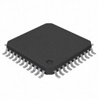
1.2
PDIP, SOIC
MCLR/VPP
RA0/AN0
RA1/AN1
RA2/AN2/VREF-/CVREF
RA3/AN3/VREF+
RA4/T0CKI/C1OUT
RA5/AN4/SS/C2OUT
Vss
OSC1/CLKI
OSC2/CLKO
RC0/T1OSO/T1CKI
RC1/T1OSI/CCP2
RC2/CCP1
RC3/SCK/SCL
MCLR/VPP
RA0/AN0
RA1/AN1
RA2/AN2/VREF-/CVREF
RA3/AN3/VREF+
RA4/T0CKI/C1OUT
RA5/AN4/SS/C2OUT
RE0/RD/AN5
RE1/WR/AN6
RE2/CS/AN7
VDD
VSS
OSC1/CLKI
OSC2/CLKO
RC0/T1OSO/T1CKI
RC1/T1OSI/CCP2
RC2/CCP1
RC3/SCK/SCL
RD0/PSP0
RD1/PSP1
1
2
3
4
5
6
7
8
9
10
11
12
13
14
1
2
3
4
5
6
7
8
9
10
11
12
13
14
15
16
17
18
19
20
PIC16F876A/873A
• PIC16F873A
Pin Diagrams
28
27
26
25
24
23
22
21
20
19
18
17
16
15
PIC16F877A/874A
This document includes programming
specifications for the following devices:
40
39
38
37
36
35
34
33
32
31
30
29
28
27
26
25
24
23
22
21
RB7/PGD
RB6/PGC
RB5
RB4
RB3/PGM
RB2
RB1
RB0/INT
VDD
VSS
RC7/RX/DT
RC6/TX/CK
RC5/SDO
RC4/SDI/SDA
RB7/PGD
RB6/PGC
RB5
RB4
RB3/PGM
RB2
RB1
RB0/INT
VDD
VSS
RD7/PSP7
RD6/PSP6
RD5/PSP5
RD4/PSP4
RC7/RX/DT
RC6/TX/CK
RC5/SDO
RC4/SDI/SDA
RD3/PSP3
RD2/PSP2
Programming Mode
The Programming mode for the PIC16F87XA allows
programming of user program memory, data memory,
special locations used for ID, and the configuration
word.
2010 Microchip Technology Inc.
Advance Information
DS39589C-page 1
�PIC16F87XA
TABLE 1-1:
PIN DESCRIPTIONS (DURING PROGRAMMING): PIC16F87XA
During Programming
Pin Name
Function
Pin Type
Pin Description
RB3
PGM
I
Low voltage ICSP™ programming input if LVP
configuration bit equals ‘1’
RB6
CLOCK
I
Clock input
RB7
DATA
I/O
MCLR
VTEST MODE
P*
Data input/output
Program Mode Select
VDD
VDD
P
Power Supply
VSS
VSS
P
Ground
Legend: I = Input, O = Output, P = Power
* To activate the Programming mode, high voltage needs to be applied to the MCLR input. Since MCLR is used for a
level source, this means that MCLR does not draw any significant current.
DS39589C-page 2
Advance Information
2010 Microchip Technology Inc.
�PIC16F87XA
2.0
PROGRAM MODE ENTRY
2.2
2.1
User Program Memory Map
The EEPROM data memory space is a separate block
of high endurance memory that the user accesses,
using a special sequence of instructions. The amount
of data EEPROM memory depends on the device and
is shown below in number of bytes.
The user memory space extends from 0000h to 1FFFh
(8 K words). In Programming mode, the program memory space extends from 0000h to 3FFFh, with the first
half (0000h - 1FFFh) being user program memory and
the second half (2000h - 3FFFh) being configuration
memory. The PC will increment from 0000h to 1FFFh
and wrap around to 0000h. From 2000h, the PC will
increment up to 3FFFh and wrap around to 2000h (not
to 0000h). Once in configuration memory, the highest
bit of the PC stays a ‘1’, thus always pointing to the configuration memory. The only way to point to user program memory is to reset the part and re-enter
Program/Verify mode, as described in Section 2.4.
In the configuration memory space, 2000h - 200Fh are
physically implemented. However, only locations
2000h through 2007h are available. Other locations are
reserved. Locations beyond 200Fh will physically
access user memory (see Figure 2-1).
2010 Microchip Technology Inc.
Data EEPROM Memory
Device
# of Bytes
PIC16F873A
128
PIC16F874A
128
PIC16F876A
256
PIC16F877A
256
The contents of data EEPROM memory have the capability to be embedded into the HEX file.
The programmer should be able to read data EEPROM
information from a HEX file and conversely (as an
option), write data EEPROM contents to a HEX file,
along with program memory information and
configuration bit information.
The 256 data memory locations are logically mapped
starting at address 2100h. The format for data memory
storage is one data byte per address location, LSB
aligned.
Advance Information
DS39589C-page 3
�PIC16F87XA
2.3
ID Locations
A user may store identification information (ID) in four
ID locations. The ID locations are mapped in addresses
2000h - 2003h. It is recommended that the user use
only the four Least Significant bits of each ID location.
In some devices, the ID locations read out in an
unscrambled fashion after code protection is enabled.
FIGURE 2-1:
For these devices, it is recommended that ID location
is written as “11 1111 1000 bbbb”, where ‘bbbb’ is
ID information.
In other devices, the ID locations read out normally,
even after code protection. To understand how the
devices behave, refer to Table 5-1.
PIC16F87XA PROGRAM MEMORY MAPPING
4K word
devices
8K word
devices
Implemented
Implemented
000h
2000h
2001h
ID Location
ID Location
Implemented
Implemented
3FFh
400h
7FFh
800h
2002h
ID Location
2003h
ID Location
2004h
Reserved
2005h
Reserved
Implemented
Implemented
Implemented
Implemented
BFFh
C00h
FFFh
1000h
Implemented
Reserved
Implemented
13FFh
1400h
17FFh
1800h
2006h
Device ID
2007h
Configuration Word
Implemented
1BFFh
1C00h
Implemented
1FFFh
2008h
Reserved
Reserved
2100h
Reserved
Reserved
3FFFh
DS39589C-page 4
Advance Information
2010 Microchip Technology Inc.
�PIC16F87XA
2.4
Program/Verify Mode
The Program/Verify mode is entered by holding pins
RB6 and RB7 low, while raising MCLR pin from VIL to
VIHH (high voltage). In this mode, the state of the RB3
pin does not effect programming. Low Voltage ICSP
Programming mode is entered by raising RB3 from VIL
to VDD, and then applying VDD to MCLR. Once in this
mode, the user program memory and the configuration
memory can be accessed and programmed in serial
fashion. The mode of operation is serial, and the memory accessed is the user program memory. RB6 and
RB7 are Schmitt Trigger inputs in this mode.
Note:
The OSC must not have 72 osc clocks
while the device MCLR is between VIL and
VIHH.
The sequence that enters the device into the Programming/Verify mode places all other logic into the RESET
state (the MCLR pin was initially at VIL). This means all
I/O are in the RESET state (high impedance inputs).
A device RESET will clear the PC and set the address
to ‘0’. The ‘Increment Address’ command will increment the PC. The ‘Load Configuration’ command will
set the PC to 2000h. The available commands are
shown in Table 2-1.
The normal sequence for programming eight program
memory words at a time is as follows:
1.
2.
3.
4.
5.
6.
7.
8.
9.
Load a word at the current program memory
address using the ‘Load Data’ command.
Issue an ‘Increment Address’ command.
Load a word at the current program memory
address using the ‘Load Data’ command.
Repeat Step 2 and Step 3 six times.
Issue a ‘Begin Programming’ command to begin
programming.
Wait tprog (about 1 ms).
Issue an ‘End Programming’ command.
Increment to the next address.
Repeat this sequence as required to write
program and configuration memory.
The alternative sequence for programming one
program memory word at a time is as follows:
1.
2.
3.
4.
5.
6.
Set a word for the current memory location using
the ‘Load Data’ command.
Issue a ‘Begin Programming Only’ command to
begin programming.
Wait tprog.
Issue an ‘End Programming’ command.
Increment to the next address.
Repeat this alternative sequence as required to
write program and configuration memory.
The address and program counter are reset to 0000h
by resetting the device (taking MCLR below VIL) and
re-entering Programming mode. Program and configuration memory may then be read or verified using the
‘Read Data’ and ‘Increment Address’ commands.
2.4.1
LOW VOLTAGE ICSP
PROGRAMMING MODE
Low Voltage ICSP Programming mode allows a
PIC16F87XA device to be programmed using VDD
only. However, when this mode is enabled by a configuration bit (LVP), the PIC16F87XA device dedicates
RB3 to control entry/exit into Programming mode.
When LVP bit is set to ‘1’, the low voltage ICSP programming entry is enabled. Since the LVP configuration bit allows low voltage ICSP programming entry in
its erased state, an erased device will have the LVP bit
enabled at the factory. While LVP is ‘1’, RB3 is dedicated to low voltage ICSP programming. Bring RB3
and then, MCLR to VDD to enter Programming mode.
All other specifications for high voltage ICSP apply.
To disable Low Voltage ICSP mode, the LVP bit must
be programmed to ‘0’. This must be done while entered
with the High Voltage Entry mode (LVP bit = ‘1’). RB3
is now a general purpose I/O pin.
2.4.2
SERIAL PROGRAM/VERIFY
OPERATION
The RB6 pin is used as a clock input pin, and the RB7
pin is used to enter command bits, and to input or output data during serial operation. To input a command,
the clock pin (RB6) is cycled six times. Each command
bit is latched on the falling edge of the clock, with the
Least Significant bit (LSb) of the command being input
first. The data on RB7 is required to have a minimum
setup (tset1) and hold (thold1) time (see AC/DC specifications), with respect to the falling edge of the clock.
Commands with associated data (read and load) are
specified to have a minimum delay (tdly1) of 1 s
between the command and the data. After this delay,
the clock pin is cycled 16 times, with the first cycle
being a Start bit (0) and the last cycle being a Stop bit
(0). Data is transferred LSb first.
During a read operation, the LSb will be transmitted
onto RB7 on the rising edge of the second cycle, and
during a load operation, the LSb will be latched on the
falling edge of the second cycle. A minimum 1 s delay
(tdly2) is specified between consecutive commands.
All commands and data words are transmitted LSb first.
The data is transmitted on the rising edge, and latched
on the falling edge of the clock. To allow decoding of
commands and reversal of data pin configuration, a
time separation of at least 1 s (tdly1) is required
between a command and a data word, or another
command.
The available commands are described in the following
paragraphs and listed in Table 2-1.
2010 Microchip Technology Inc.
Advance Information
DS39589C-page 5
�PIC16F87XA
2.4.2.1
Load Configuration
2.4.2.7
After receiving this command, the program counter
(PC) will be set to 2000h. By then applying 16 cycles to
the clock pin, the chip will load 14 bits in a “data word,”
as described above, to be programmed into the configuration memory. A description of the memory mapping
schemes of the program memory for normal operation
and configuration mode operation is shown in
Figure 2-1. After the configuration memory is entered,
the only way to get back to the user program memory
is to exit the Program/Verify Test mode by taking MCLR
low (VIL).
2.4.2.2
Load Data for Program Memory
After receiving this command, the chip will load one
word (with 14 bits as a “data word”) to be programmed
into user program memory when 16 cycles are applied.
A timing diagram for this command is shown in
Figure 6-1.
2.4.2.3
2.4.2.4
Read Data from Program Memory
After receiving this command, the chip will transmit
data bits out of the program memory (user or configuration) currently accessed, starting with the second rising edge of the clock input. The RB7 pin will go into
Output mode on the second rising clock edge, and it
will revert back to Input mode (high-impedance) after
the 16th rising edge. A timing diagram of this command
is shown in Figure 6-3.
2.4.2.5
Read Data from Data Memory
After receiving this command, the chip will transmit
data bits out of the data memory, starting with the second rising edge of the clock input. The RB7 pin will go
into Output mode on the second rising edge, and it will
revert back to Input mode (high-impedance) after the
16th rising edge. As previously stated, the data memory is 8-bits wide, and therefore, only the first 8 bits that
are output are actual data. A timing diagram for this
command is shown in Figure 6-4.
2.4.2.6
Eight locations must be loaded before every
‘Begin Erase/Programming’ command. After this
command is received and decoded, eight words of
program memory will be erased and programmed with
the values contained in the program data latches. The
PC address will decode which eight words are programmed. The lower three bits of the PC are ignored,
so if the PC points to address 003h, then all eight
locations from 000h to 007h are written.
An internal timing mechanism executes an erase
before write. The user must allow the combined time
for erase and programming, as specified in the electrical specs, for programming to complete. No ‘End
Programming’ command is required.
1.
2.
Load Data for Data Memory
After receiving this command, the chip will load in a
14-bit “data word” when 16 cycles are applied.
However, the data memory is only 8-bits wide, and
thus, only the first 8 bits of data after the Start bit will be
programmed into the data memory. It is still necessary
to cycle the clock the full 16 cycles in order to allow the
internal circuitry to reset properly. The data memory
contains up to 256 bytes. If the device is
code-protected, the data is read as all zeros. A timing
diagram for this command is shown in Figure 6-2.
Increment Address
The PC is incremented when this command is
received. A timing diagram of this command is shown
in Figure 6-5.
DS39589C-page 6
Begin Erase/Program Cycle
If the address is pointing to user memory, the
user memory alone will be affected.
If the address is pointing to the physically implemented test memory (2000h - 201Fh), test memory will be written. The configuration word will not
be written unless the address is specifically
pointing to 2007h.
This command can be used to perform programming
over the entire VDD range of the device.
Note 1: The code-protect bits cannot be erased
with this command.
2: All Begin Erase/Programming operations
can take place over the entire VDD range.
A timing diagram for this command is shown in
Figure 6-6.
2.4.2.8
Note:
Begin Programming Only
Begin Programming Only operations must
take place at the 4.5V to 5.5V VDD range.
This command is similar to the ‘Erase/Programming
Cycle’ command, except that a word erase is not
done, and the internal timer is not used. Programming
of program and data memory will begin after this command is received and decoded. The user must allow
the time for programming, as specified in the electrical
specs, for programming to complete. An ‘End
Programming’ command is required.
The internal timer is not used for this command, so the
‘End Programming’ command must be used to stop
programming.
1.
2.
If the address is pointing to user memory, the
user memory alone will be affected.
If the address is pointing to the physically implemented test memory (2000h - 201Fh), the test
memory will be written. The configuration word
will not be written unless the address is
specifically pointing to 2007h.
A timing diagram for this command is shown in
Figure 6-7.
Advance Information
2010 Microchip Technology Inc.
�PIC16F87XA
2.4.2.9
End Programming
After receiving this command, the chip stops programming the memory (test program memory or user program memory) that it was programming at the time.
Note:
This command will also set the write data
shift latches to all ‘1’s to avoid issues with
downloading only one word before the
write.
TABLE 2-1:
COMMAND MAPPING FOR PIC16F87XA
Command
Mapping (MSB … LSB)
Data
Voltage Range
Load Configuration
0
0
0
0
0
0, data (14), 0
2.2V - 5.5V
Load Data for Program Memory
0
0
0
1
0
0, data (14), 0
2.2V - 5.5V
0, data (14), 0
2.2V - 5.5V
Read Data from Program Memory
0
0
1
0
0
Increment Address
0
0
1
1
0
Begin Erase/Programming Cycle
0
1
0
0
0
4 ms typical,
internally timed
2.2V - 5.5V
Begin Programming Only Cycle
1
1
0
0
0
1 ms typical,
externally timed
4.5V - 5.5V
Bulk Erase Program Memory
0
1
0
0
1
internally timed
4.5V - 5.5V
2.2V - 5.5V
Bulk Erase Data Memory
0
1
0
1
1
internally timed
4.5V - 5.5V
Chip Erase
1
1
1
1
1
4 ms typical,
internally timed
4.5V - 5.5V
Load Data for Data Memory
0
0
0
1
1
0, data (14), 0
2.2V - 5.5V
Read Data from Data Memory
0
0
1
0
1
0, data (14), 0
2.2V - 5.5V
End Programming
1
0
1
1
1
2010 Microchip Technology Inc.
Advance Information
DS39589C-page 7
�PIC16F87XA
2.5
Erasing Program and Data
Memory
Depending on the state of the code protection bits, program and data memory will be erased using different
methods. The first two commands are used when both
program and data memories are not code-protected.
The third command is used when either memory is
code-protected, or if you want to also erase the fuse
locations, including the code-protect bits. A device programmer should determine the state of the code protection bits and then apply the proper command to
erase the desired memory.
2.5.1
ERASING NON-CODE PROTECTED
PROGRAM AND DATA MEMORY
When both program and data memories are not
code-protected, they must be individually erased using
the following commands. The only way that both memories are erased using a single command is if code protection is enabled for one of the memories. These
commands do not erase the configuration word or ID
locations.
2.5.1.1
Bulk Erase Program Memory
When this command is performed, and is followed by
a ‘Begin Erase/Programming’ command, the entire
program memory will be erased.
If the address is pointing to user memory, only the user
memory will be erased.
If the address is pointing to the test program memory
(2000h - 201Fh), then both the user memory and the
test memory will be erased. The configuration word
will not be erased, even if the address is pointing to
location 2007h.
Previously, a load data with 0FFh command was recommended before any Bulk Erase. On these devices,
this will not be required.
The Bulk Erase command is disabled when the CP bit
is programmed to ‘0’ enabling code-protect.
A timing diagram for this command is shown in
Figure 6-8.
2.5.1.2
Bulk Erase Data Memory
When this command is performed, and is followed by
a ‘Begin Erase/Programming’ command, the entire
data memory will be erased.
The Bulk Erase Data command is disabled when the
CPD bit is programmed to ‘0’ enabling protected data
memory. A timing diagram for this command is shown
in Figure 6-9.
Note:
All Bulk Erase operations must take place
at the 4.5V to 5.5V VDD range.
DS39589C-page 8
2.5.1.3
Chip Erase
This command, when performed, will erase the program memory, EE data memory, and all of the fuse
locations, including the code protection bits. All
on-chip Flash and EEPROM memory is erased,
regardless of the address contained in the PC.
When a Chip Erase command is issued and the PC
points to (0000h - 1FFFh), the configuration word and
the user program memory will be erased, but not the
test row (see Section 2.5.2.1). Chip Erase can also be
used to erase code-protected memory, as described in
Section 2.5.2.
This command will also erase the code-protect and
code-protect data fuses if they are programmed. This
is the only command that allows a user to erase the
code-protect fuses.
The Chip Erase is internally self-timed to ensure that
all program and data memory is erased before the
code-protect bits are erased. A timing diagram for this
command is shown in Figure 6-10.
Note:
2.5.2
The Chip Erase operation must take place
at the 4.5V to 5.5V VDD range.
ERASING CODE PROTECTED
MEMORY
For the PIC16F87XA devices, once code protection is
enabled, all protected program and data memory locations read all ‘0’s and further programming is disabled.
The ID locations and configuration word read out
unscrambled and can be reprogrammed normally. The
only command to erase a code-protected PIC16F87XA
device is the Chip Erase. This erases program memory, data memory, configuration bits and ID locations.
Since all data within the program and data memory
will be erased when this command is executed, the
security of the data or code is not compromised.
2.5.2.1
Chip Erase
This command, when performed, will erase the program memory, data EEPROM, and all of the fuse locations, including the code protection bits, code-protect
fuses, and code-protect data fuses. All on-chip Flash
and EEPROM memory is erased, regardless of the
address contained in the PC.
If the PC points to user memory, the test row (2000h
through 201Fh) is not erased with a Chip Erase command, except for the configuration word (at 2007h). If
the test row is to be completely erased, the address in
the PC must point to configuration memory.
When the PC points to 2000h - 201Fh, the configuration word, test program memory, and the user program
memory will all be erased with a Chip Erase command.
This allows the user to erase all program and configuration content, including the code-protect bits, without
compromising the user ID bits (2000h through 2004h),
or any pass codes stored in the test row.
Advance Information
2010 Microchip Technology Inc.
�PIC16F87XA
The Chip Erase is internally self-timed to ensure that all
program and data memory is erased before the
code-protect bits are erased.
FIGURE 2-2:
A timing diagram for this command is shown in
Figure 6-10.
Note:
The Chip Erase operation must take place
at the 4.5V to 5.5V VDD range.
ALGORITHM 1 FLOWCHART – PROGRAM MEMORY (2.0V VDD < 5.5V)
Start
Set VDD = VDDP
Load Data
Command
Increment
Address
Command
No
Eight Loads
Done?
Yes
Begin
Erase/Programming
Command
Wait tprog2
(8 ms)
Increment
Address
Command
No
All Locations
Done?
Verify all
Locations
Report Verify
Error
No
Data Correct?
End
2010 Microchip Technology Inc.
Advance Information
DS39589C-page 9
�PIC16F87XA
FIGURE 2-3:
ALGORITHM 2 FLOWCHART – PROGRAM MEMORY (4.5V VDD 5.5V)
Start
Chip Erase
Sequence
Set VDD = VDDP
Load Data
Command
Increment
Address
Command
No
Eight Loads
Done?
Yes
Begin
Programming Only
Command
Wait tprog1
(1 ms)
End
Programming
Command
Increment
Address
Command
No
All Locations
Done?
Yes
Verify all
Locations
Report Verify
Error
No
Data Correct?
Yes
End
DS39589C-page 10
Advance Information
2010 Microchip Technology Inc.
�PIC16F87XA
FLOWCHART – PIC16F87XA CONFIGURATION MEMORY (2.0V VDD < 5.5V)
FIGURE 2-4:
PROGRAM
FOUR LOCATIONS
Start
Start
Load
Configuration
Data
(Set PC=2000h)
Load
Configuration
Data
Yes
Program ID
Location?
Program Four
Locations
Read Data
Command
No
Load Data
Command
Increment
Address
Command
No
Four Loads
Done?
Yes
Report
Programming
Failure
No
Data Correct?
Yes
Yes
Increment
Address
Command
Begin
Erase/Program
Command
Address =
2003h?
Wait tprog2
(8 ms)
No
Address =
2004h?
No
Increment
Address
Command
End
Yes
PROGRAM
CONFIGURATION WORD
Increment
Address
Command
Start
Increment
Address
Command
Report Program
Configuration
Word Error
No
Load Data
Command
Increment
Address
Command
Program
(Config. Word)
Data Correct?
Read Data
Command
Begin
Erase/Program
Command
Wait tprog2
(8 ms)
Yes
End
End
2010 Microchip Technology Inc.
Advance Information
DS39589C-page 11
�PIC16F87XA
FLOWCHART – PIC16F87XA CONFIGURATION MEMORY (4.5V VDD 5.5V)
FIGURE 2-5:
PROGRAM
FOUR LOCATIONS
Start
Start
Load
Configuration
Data
(Set PC=2000h)
Load Data
Command
Load
Configuration
Data
Chip Erase
Yes
Program ID
Location?
Read Data
Command
Program Four
Locations
No
Report
Programming
Failure
No
Data Correct?
Increment
Address
Command
No
Four Loads
Done?
Yes
Begin
Program Only
Command
Yes
Yes
Increment
Address
Command
No
No
Address =
2004h?
Wait tprog1
(1 ms)
Address =
2003h?
Increment
Address
Command
End
Programming
Command
End
Yes
Increment
Address
Command
PROGRAM
CONFIGURATION WORD
Start
Increment
Address
Command
Report Program
Configuration
Word Error
No
Load Data
Command
Increment
Address
Command
Program
(Config. Word)
Data Correct?
Read Data
Command
Begin
Erase/Program
Command
Wait tprog2
(8 ms)
Yes
End
DS39589C-page 12
End
Advance Information
2010 Microchip Technology Inc.
�PIC16F87XA
3.0
CONFIGURATION WORD
TABLE 3-1:
The PIC16F87XA has several configuration bits. These
bits can be set (reads ‘0’), or left unchanged (reads ‘1’),
to select various device configurations.
3.1
The device ID word for the PIC16F87XA is located at
2006h.
R/P-1
U-1
CP
—
Device ID Value
Device
Device ID Word
REGISTER 3-1:
DEVICE ID VALUE
Dev
Rev
PIC16F873A
00 1110 0100
XXXX
PIC16F874A
00 1110 0110
XXXX
PIC16F876A
00 1110 0000
XXXX
PIC16F877A
00 1110 0010
XXXX
CONFIGURATION WORD REGISTER
R/P-1
R/P-1
R/P-1
R/P-1
R/P-1
U-1
U-1
DEBUG WRT1
R/P-1
WRT0
CPD
LVP
BOREN
—
—
R/P-1
R/P-1
R/P-1
R/P-1
PWRTEN WDTEN FOSC1 FOSC0
bit 13
bit 0
bit 13
CP: Flash Program Memory Code Protection bit
(PIC16F877A/876A):
1 = Code protection off
0 = 0000h to 1FFFh code-protected
(PIC16F874A/873A):
1 = Code protection off
0 = 0000h to 0FFFh code-protected
1000h to 1FFFh wraps to 0000h to 0FFFh
bit 12
Unimplemented: Read as ‘1’
bit 11
DEBUG: Background Debugger Mode bit
1 = Background debugger functions not enabled
0 = Background debugger functional
bit 10-9
WRT: Flash Program Memory Write Enable bits
(PIC16F877A/876A):
11 = Write protection off
10 = 0000h to 00FFh write protected, 0100h to 1FFFh may be modified by EECON control
01 = 0000h to 07FFh write protected, 0800h to 1FFFh may be modified by EECON control
00 = 0000h to 0FFFh write protected, 1000h to 1FFFh may be modified by EECON control
(PIC16F874A/873A):
11 = Write protection off
10 = 0000h to 00FFh write protected, 0100h to 0FFFh may be modified by EECON control
01 = 0000h to 03FFh write protected, 0400h to 0FFFh may be modified by EECON control
00 = 0000h to 07FFh write protected, 0800h to 1FFFh may be modified by EECON control
bit 8
CPD: Data EE Memory Code Protection bit
1 = Code protection off
0 = Data EE memory code-protected
bit 7
LVP: Low Voltage Programming Enable bit
1 = RB3/PGM pin has PGM function, low voltage programming enabled
0 = RB3 is digital I/O, HV on MCLR must be used for programming
bit 6
BOREN: Brown-out Reset Enable bit
1 = BOR enabled
0 = BOR disabled
bit 5-4
Unimplemented: Read as ‘1’
bit 3
PWRTEN: Power-up Timer Enable bit
1 = PWRT disabled
0 = PWRT enabled
bit 2
WDTEN: Watchdog Timer Enable bit
1 = WDT enabled
0 = WDT disabled
bit 1-0
FOSC: Oscillator Selection bits
11 = RC oscillator
10 = HS oscillator
01 = XT oscillator
00 = LP oscillator
Legend:
R = Readable bit
W = Writable bit
U = Unimplemented bit, read as ‘1’
-n = Default value
1 = Bit is erased
0 = Bit is programmed
2010 Microchip Technology Inc.
Advance Information
x = Bit is unknown
DS39589C-page 13
�PIC16F87XA
4.0
EMBEDDING CONFIGURATION WORD AND ID INFORMATION IN HEX FILE
To allow portability of code, the programmer is required to read the configuration word and ID locations from the HEX
file when loading the HEX file. If configuration word information was not present in the HEX file, then a simple warning
message may be issued. Similarly, while saving a HEX file, configuration word and ID information must be included.
An option to not include this information may be provided.
Specifically for the PIC16F87XA, the EEPROM data memory should also be embedded in the HEX file (see
Section 2.2).
Microchip Technology Inc. feels strongly that this feature is important for the benefit of the end customer.
DS39589C-page 14
Advance Information
2010 Microchip Technology Inc.
�PIC16F87XA
5.0
CHECKSUM COMPUTATION
The Least Significant 16 bits of this sum are the
checksum.
Checksum is calculated by reading the contents of the
PIC16F87XA memory locations and adding up the
opcodes up to the maximum user addressable location,
e.g., 0x1FF for the PIC16F87XA. Any carry bits
exceeding 16-bits are neglected. Finally, the configuration word (appropriately masked) is added to the
checksum. Checksum computation for each member of
the PIC16F87XA devices is shown in Table 5-1.
The following table describes how to calculate the
checksum for each device. Note that the checksum calculation differs depending on the code-protect setting.
Since the program memory locations read out differently depending on the code-protect setting, the table
describes how to manipulate the actual program memory values to simulate the values that would be read
from a protected device. When calculating a checksum
by reading a device, the entire program memory can
simply be read and summed. The configuration word
and ID locations can always be read.
The checksum is calculated by summing the following:
• The contents of all program memory locations
• The configuration word, appropriately masked
• Masked ID locations (when applicable)
TABLE 5-1:
CHECKSUM COMPUTATION
Blank
Value
25E6h at 0
and max
address
SUM[0000:0FFF] + (CFGW & 2FCF)
1FCF
EB9D
(CFGW & 2FCF) + SUM_ID
4F9E
1B6C
OFF
SUM[0000:0FFF] + (CFGW & 2FCF)
1FCF
EB9D
ON
(CFGW & 2FCF) + SUM_ID
4F9E
1B6C
OFF
SUM[0000:1FFF] + (CFGW & 2FCF)
0FCF
DB9D
ON
(CFGW & 2FCF) + SUM_ID
1F9E
EB6C
OFF
SUM[0000:1FFF] + (CFGW & 2FCF)
0FCF
DB9D
ON
(CFGW & 2FCF) + SUM_ID
1F9E
EB6C
Device
Code
Protect
PIC16F873A
OFF
ON
PIC16F874A
PIC16F876A
PIC16F877A
Legend: CFGW
SUM[a:b]
SUM_ID
Note that some older devices have an additional value
added in the checksum. This is to maintain compatibility
with older device programmer checksums.
=
=
=
*Checksum =
+
=
&
=
Checksum*
Configuration Word
[Sum of locations a to b inclusive]
ID locations masked by 0Fh then made into a 16-bit value with ID0 as the most significant nibble.
For example, ID0 = 01h, ID1 = 02h, ID3 = 03h, ID4 = 04h, then SUM_ID = 1234h
[Sum of all the individual expressions] MODULO [FFFFh]
Addition
Bitwise AND
2010 Microchip Technology Inc.
Advance Information
DS39589C-page 15
�PIC16F87XA
6.0
PROGRAM/VERIFY MODE ELECTRICAL CHARACTERISTICS
TABLE 6-1:
TIMING REQUIREMENTS FOR PROGRAM/VERIFY MODE
AC/DC CHARACTERISTICS
POWER SUPPLY PINS
Characteristics
Standard Operating Procedure (unless otherwise stated)
Operating temperature
0 TA +70°C
Operating Voltage
2.0V VDD 5.5V
Sym
Min
Typ
Max
Units
Conditions/Comments
General
VDD level for Begin Erase/Program
operations and EECON write of
program memory
VDD
2.0
—
5.5
V
VDD level for Begin Erase/Program
operations and EECON write of data
memory
VDD
2.0
—
5.5
V
VDD level for Bulk Erase/Write, Chip
VDD
Erase, and Begin Program operations,
of program and data memory
4.5
—
5.5
V
Begin Programming Only cycle time
tprog1
1
—
—
ms
Externally Timed
Begin Erase/Programming
tprog2
10 ms
—
—
ms
Internally Timed
Chip Erase cycle time
tprog3
10 ms
—
—
ms
Internally Timed
High voltage on MCLR and
RA4/T0CKI for Test mode entry
VIHH
VDD + 3.5
—
13.5
V
MCLR rise time (VSS to VHH) for
Test mode entry
tVHHR
—
—
1.0
s
(RB6, RB7) input high level
VIH1
0.8 VDD
—
—
V
Schmitt Trigger input
(RB6, RB7) input low level
VIL1
0.2 VDD
—
—
V
Schmitt Trigger input
RB setup time before MCLR
(Test mode selection pattern setup
time)
tset0
100
—
—
ns
RB hold time after MCLR (Test
mode selection pattern setup time)
thld0
5
—
—
s
Data in setup time before clock
tset1
100
—
—
ns
Data in hold time after clock
thld1
100
—
—
ns
Data input not driven to next clock input tdly1
(delay required between
command/data or command/command)
1.0
—
—
s
2.0V VDD < 4.5V
100
—
—
ns
4.5V VDD 5.5V
1.0
—
—
s
2.0V VDD < 4.5V
100
—
—
ns
4.5V VDD 5.5V
80
—
—
ns
Serial Program/Verify
Delay between clock to clock
of next command or data
tdly2
Clock to data out valid
(during read data)
tdly3
DS39589C-page 16
Advance Information
2010 Microchip Technology Inc.
�PIC16F87XA
FIGURE 6-1:
LOAD DATA FOR USER PROGRAM MEMORY COMMAND (PROGRAM/VERIFY)
VIHH
1 s min
MCLR
tset0
1
2
3
4
5
6
1
tdly2
RB6
(CLOCK)
2
3
4
5
15
16
thld0
1
0
RB7
(DATA)
0
0
0
strt_bit
X
tset1
stp_bit
tset1
tdly1
1 s min
thld1
}
}
}
}
thld1
100 ns min
100 ns min
Program/Verify Test Mode
RESET
FIGURE 6-2:
LOAD DATA FOR USER DATA MEMORY COMMAND (PROGRAM/VERIFY)
VIHH
1 s min
MCLR
tset0
1
2
3
4
5
6
1
tdly2
RB6
(CLOCK)
2
3
4
5
15
16
thld0
1
1
RB7
(DATA)
0
0
0
tset1
strt_bit
X
stp_bit
tset1
tdly1
1 s min
thld1
}
}
}
}
thld1
100 ns min
100 ns min
Program/Verify Test Mode
RESET
FIGURE 6-3:
READ DATA FROM PROGRAM MEMORY COMMAND (PROGRAM/VERIFY)
VIHH
MCLR
tset0
tdly2
thld0
1
1 s min
2
3
4
5
6
1
2
3
RB6
(CLOCK)
RB7
(DATA)
4
5
15
16
tdly3
0
0
1
0
0
bit 13
bit 0
X
tdly1
tset1
thld1
}
}
1 s min
100 ns min
RB7 = output
RB7 = input
RESET
2010 Microchip Technology Inc.
RB7
input
Program/Verify Test Mode
Advance Information
DS39589C-page 17
�PIC16F87XA
FIGURE 6-4:
READ DATA FROM DATA MEMORY COMMAND (PROGRAM/VERIFY)
VIHH
MCLR
tdly2
tset0
thld0
1
1 s min
2
3
4
5
1
0
6
1
2
3
RB6
(CLOCK)
4
5
15
16
tdly3
RB7
(DATA)
1
0
tset1
0
bit 13
bit 0
X
tdly1
thld1
}
}
1 s min
100 ns min
RB7 = input
RB7 = output
RB7
input
Program/Verify Test Mode
RESET
FIGURE 6-5:
INCREMENT ADDRESS COMMAND (PROGRAM/VERIFY)
VIHH
MCLR
tdly2
1 s min
1
2
3
4
5
6
Next Command
1
2
RB6
(CLOCK)
RB7
(DATA)
0
1
0
1
tset1
0
0
tdly1
thld1
}
}
1 s min
100 ns min
Program/Verify Test Mode
RESET
FIGURE 6-6:
X
X
BEGIN ERASE/PROGRAMING COMMAND (PROGRAM/VERIFY)
VIHH
MCLR
tprog2
Next Command
1
2
3
4
5
1
6
2
RB6
(CLOCK)
RB7
(DATA)
0
0
0
1
tset1
0
thld1
X
X
0
tdly1
}
}
100 ns min
RESET
DS39589C-page 18
Program/Verify Test Mode
Advance Information
2010 Microchip Technology Inc.
�PIC16F87XA
FIGURE 6-7:
BEGIN PROGRAMING ONLY COMMAND (PROGRAM/VERIFY)
VIHH
MCLR
tprog1
1
2
3
4
5
End Programming Command
1
2
6
6
RB6
(CLOCK)
tdly2
1 s min
RB7
(DATA)
0
0
0
1
1
X
1
0
tdly1
tset1
thld1
}
}
100 ns min
Program/Verify Test Mode
RESET
FIGURE 6-8:
BULK ERASE PROGRAM MEMORY COMMAND (PROGRAM/VERIFY)
VIHH
MCLR
tdly2
1
2
3
4
5
6
1 s min
1
Begin Erase/Programming
Command
2
RB6
(CLOCK)
RB7
(DATA)
1
0
1
0
0
X
tset1
X
0
tdly1
thld1
}
}
100 ns min
Program/Verify Test Mode
RESET
FIGURE 6-9:
BULK ERASE DATA MEMORY COMMAND (PROGRAM/VERIFY)
VIHH
MCLR
tdly2
1
2
3
4
5
6
1 s min
1
Begin Erase/Programming
Command
2
RB6
(CLOCK)
RB7
(DATA)
1
1
0
1
0
X
X
0
tdly1
tset1
thld1
}
}
100 ns min
RESET
2010 Microchip Technology Inc.
Program/Verify Test Mode
Advance Information
DS39589C-page 19
�PIC16F87XA
FIGURE 6-10:
CHIP ERASE COMMAND (PROGRAM/VERIFY)
VIHH
MCLR
tprog3
Next Command
1
2
3
1
1
1
4
5
6
1
X
1
2
RB6
(CLOCK)
RB7
(DATA)
1
tdly1
X
0
tset1
thld1
}
}
100 ns min
RESET
DS39589C-page 20
Program/Verify Test Mode
Advance Information
2010 Microchip Technology Inc.
�Note the following details of the code protection feature on Microchip devices:
•
Microchip products meet the specification contained in their particular Microchip Data Sheet.
•
Microchip believes that its family of products is one of the most secure families of its kind on the market today, when used in the
intended manner and under normal conditions.
•
There are dishonest and possibly illegal methods used to breach the code protection feature. All of these methods, to our
knowledge, require using the Microchip products in a manner outside the operating specifications contained in Microchip’s Data
Sheets. Most likely, the person doing so is engaged in theft of intellectual property.
•
Microchip is willing to work with the customer who is concerned about the integrity of their code.
•
Neither Microchip nor any other semiconductor manufacturer can guarantee the security of their code. Code protection does not
mean that we are guaranteeing the product as “unbreakable.”
Code protection is constantly evolving. We at Microchip are committed to continuously improving the code protection features of our
products. Attempts to break Microchip’s code protection feature may be a violation of the Digital Millennium Copyright Act. If such acts
allow unauthorized access to your software or other copyrighted work, you may have a right to sue for relief under that Act.
Information contained in this publication regarding device
applications and the like is provided only for your convenience
and may be superseded by updates. It is your responsibility to
ensure that your application meets with your specifications.
MICROCHIP MAKES NO REPRESENTATIONS OR
WARRANTIES OF ANY KIND WHETHER EXPRESS OR
IMPLIED, WRITTEN OR ORAL, STATUTORY OR
OTHERWISE, RELATED TO THE INFORMATION,
INCLUDING BUT NOT LIMITED TO ITS CONDITION,
QUALITY, PERFORMANCE, MERCHANTABILITY OR
FITNESS FOR PURPOSE. Microchip disclaims all liability
arising from this information and its use. Use of Microchip
devices in life support and/or safety applications is entirely at
the buyer’s risk, and the buyer agrees to defend, indemnify and
hold harmless Microchip from any and all damages, claims,
suits, or expenses resulting from such use. No licenses are
conveyed, implicitly or otherwise, under any Microchip
intellectual property rights.
Trademarks
The Microchip name and logo, the Microchip logo, dsPIC,
KEELOQ, KEELOQ logo, MPLAB, PIC, PICmicro, PICSTART,
rfPIC and UNI/O are registered trademarks of Microchip
Technology Incorporated in the U.S.A. and other countries.
FilterLab, Hampshire, HI-TECH C, Linear Active Thermistor,
MXDEV, MXLAB, SEEVAL and The Embedded Control
Solutions Company are registered trademarks of Microchip
Technology Incorporated in the U.S.A.
Analog-for-the-Digital Age, Application Maestro, CodeGuard,
dsPICDEM, dsPICDEM.net, dsPICworks, dsSPEAK, ECAN,
ECONOMONITOR, FanSense, HI-TIDE, In-Circuit Serial
Programming, ICSP, Mindi, MiWi, MPASM, MPLAB Certified
logo, MPLIB, MPLINK, mTouch, Octopus, Omniscient Code
Generation, PICC, PICC-18, PICDEM, PICDEM.net, PICkit,
PICtail, PIC32 logo, REAL ICE, rfLAB, Select Mode, Total
Endurance, TSHARC, UniWinDriver, WiperLock and ZENA
are trademarks of Microchip Technology Incorporated in the
U.S.A. and other countries.
SQTP is a service mark of Microchip Technology Incorporated
in the U.S.A.
All other trademarks mentioned herein are property of their
respective companies.
© 2010, Microchip Technology Incorporated, Printed in the
U.S.A., All Rights Reserved.
Printed on recycled paper.
Microchip received ISO/TS-16949:2002 certification for its worldwide
headquarters, design and wafer fabrication facilities in Chandler and
Tempe, Arizona; Gresham, Oregon and design centers in California
and India. The Company’s quality system processes and procedures
are for its PIC® MCUs and dsPIC® DSCs, KEELOQ® code hopping
devices, Serial EEPROMs, microperipherals, nonvolatile memory and
analog products. In addition, Microchip’s quality system for the design
and manufacture of development systems is ISO 9001:2000 certified.
2010 Microchip Technology Inc.
Advance Information
DS39589C-page 21
�WORLDWIDE SALES AND SERVICE
AMERICAS
ASIA/PACIFIC
ASIA/PACIFIC
EUROPE
Corporate Office
2355 West Chandler Blvd.
Chandler, AZ 85224-6199
Tel: 480-792-7200
Fax: 480-792-7277
Technical Support:
http://support.microchip.com
Web Address:
www.microchip.com
Asia Pacific Office
Suites 3707-14, 37th Floor
Tower 6, The Gateway
Harbour City, Kowloon
Hong Kong
Tel: 852-2401-1200
Fax: 852-2401-3431
India - Bangalore
Tel: 91-80-3090-4444
Fax: 91-80-3090-4123
India - New Delhi
Tel: 91-11-4160-8631
Fax: 91-11-4160-8632
Austria - Wels
Tel: 43-7242-2244-39
Fax: 43-7242-2244-393
Denmark - Copenhagen
Tel: 45-4450-2828
Fax: 45-4485-2829
India - Pune
Tel: 91-20-2566-1512
Fax: 91-20-2566-1513
France - Paris
Tel: 33-1-69-53-63-20
Fax: 33-1-69-30-90-79
Japan - Yokohama
Tel: 81-45-471- 6166
Fax: 81-45-471-6122
Germany - Munich
Tel: 49-89-627-144-0
Fax: 49-89-627-144-44
Atlanta
Duluth, GA
Tel: 678-957-9614
Fax: 678-957-1455
Boston
Westborough, MA
Tel: 774-760-0087
Fax: 774-760-0088
Chicago
Itasca, IL
Tel: 630-285-0071
Fax: 630-285-0075
Cleveland
Independence, OH
Tel: 216-447-0464
Fax: 216-447-0643
Dallas
Addison, TX
Tel: 972-818-7423
Fax: 972-818-2924
Detroit
Farmington Hills, MI
Tel: 248-538-2250
Fax: 248-538-2260
Kokomo
Kokomo, IN
Tel: 765-864-8360
Fax: 765-864-8387
Los Angeles
Mission Viejo, CA
Tel: 949-462-9523
Fax: 949-462-9608
Santa Clara
Santa Clara, CA
Tel: 408-961-6444
Fax: 408-961-6445
Toronto
Mississauga, Ontario,
Canada
Tel: 905-673-0699
Fax: 905-673-6509
Australia - Sydney
Tel: 61-2-9868-6733
Fax: 61-2-9868-6755
China - Beijing
Tel: 86-10-8528-2100
Fax: 86-10-8528-2104
China - Chengdu
Tel: 86-28-8665-5511
Fax: 86-28-8665-7889
Korea - Daegu
Tel: 82-53-744-4301
Fax: 82-53-744-4302
China - Chongqing
Tel: 86-23-8980-9588
Fax: 86-23-8980-9500
Korea - Seoul
Tel: 82-2-554-7200
Fax: 82-2-558-5932 or
82-2-558-5934
China - Hong Kong SAR
Tel: 852-2401-1200
Fax: 852-2401-3431
Malaysia - Kuala Lumpur
Tel: 60-3-6201-9857
Fax: 60-3-6201-9859
China - Nanjing
Tel: 86-25-8473-2460
Fax: 86-25-8473-2470
Malaysia - Penang
Tel: 60-4-227-8870
Fax: 60-4-227-4068
China - Qingdao
Tel: 86-532-8502-7355
Fax: 86-532-8502-7205
Philippines - Manila
Tel: 63-2-634-9065
Fax: 63-2-634-9069
China - Shanghai
Tel: 86-21-5407-5533
Fax: 86-21-5407-5066
Singapore
Tel: 65-6334-8870
Fax: 65-6334-8850
China - Shenyang
Tel: 86-24-2334-2829
Fax: 86-24-2334-2393
Taiwan - Hsin Chu
Tel: 886-3-6578-300
Fax: 886-3-6578-370
China - Shenzhen
Tel: 86-755-8203-2660
Fax: 86-755-8203-1760
Taiwan - Kaohsiung
Tel: 886-7-536-4818
Fax: 886-7-536-4803
China - Wuhan
Tel: 86-27-5980-5300
Fax: 86-27-5980-5118
Taiwan - Taipei
Tel: 886-2-2500-6610
Fax: 886-2-2508-0102
China - Xian
Tel: 86-29-8833-7252
Fax: 86-29-8833-7256
Thailand - Bangkok
Tel: 66-2-694-1351
Fax: 66-2-694-1350
Italy - Milan
Tel: 39-0331-742611
Fax: 39-0331-466781
Netherlands - Drunen
Tel: 31-416-690399
Fax: 31-416-690340
Spain - Madrid
Tel: 34-91-708-08-90
Fax: 34-91-708-08-91
UK - Wokingham
Tel: 44-118-921-5869
Fax: 44-118-921-5820
China - Xiamen
Tel: 86-592-2388138
Fax: 86-592-2388130
China - Zhuhai
Tel: 86-756-3210040
Fax: 86-756-3210049
01/05/10
DS39589C-page 22
Advance Information
2010 Microchip Technology Inc.
�


 工商网监
湘ICP备2023018690号
工商网监
湘ICP备2023018690号