PIC16F946
Data Sheet
64-Pin Flash-Based, 8-Bit
CMOS Microcontrollers with
LCD Driver and nanoWatt Technology
© 2005 Microchip Technology Inc.
Preliminary
DS41265A
�Note the following details of the code protection feature on Microchip devices:
•
Microchip products meet the specification contained in their particular Microchip Data Sheet.
•
Microchip believes that its family of products is one of the most secure families of its kind on the market today, when used in the
intended manner and under normal conditions.
•
There are dishonest and possibly illegal methods used to breach the code protection feature. All of these methods, to our
knowledge, require using the Microchip products in a manner outside the operating specifications contained in Microchip’s Data
Sheets. Most likely, the person doing so is engaged in theft of intellectual property.
•
Microchip is willing to work with the customer who is concerned about the integrity of their code.
•
Neither Microchip nor any other semiconductor manufacturer can guarantee the security of their code. Code protection does not
mean that we are guaranteeing the product as “unbreakable.”
Code protection is constantly evolving. We at Microchip are committed to continuously improving the code protection features of our
products. Attempts to break Microchip’s code protection feature may be a violation of the Digital Millennium Copyright Act. If such acts
allow unauthorized access to your software or other copyrighted work, you may have a right to sue for relief under that Act.
Information contained in this publication regarding device
applications and the like is provided only for your convenience
and may be superseded by updates. It is your responsibility to
ensure that your application meets with your specifications.
MICROCHIP MAKES NO REPRESENTATIONS OR WARRANTIES OF ANY KIND WHETHER EXPRESS OR IMPLIED,
WRITTEN OR ORAL, STATUTORY OR OTHERWISE,
RELATED TO THE INFORMATION, INCLUDING BUT NOT
LIMITED TO ITS CONDITION, QUALITY, PERFORMANCE,
MERCHANTABILITY OR FITNESS FOR PURPOSE.
Microchip disclaims all liability arising from this information and
its use. Use of Microchip’s products as critical components in
life support systems is not authorized except with express
written approval by Microchip. No licenses are conveyed,
implicitly or otherwise, under any Microchip intellectual property
rights.
Trademarks
The Microchip name and logo, the Microchip logo, Accuron,
dsPIC, KEELOQ, microID, MPLAB, PIC, PICmicro, PICSTART,
PRO MATE, PowerSmart, rfPIC, and SmartShunt are
registered trademarks of Microchip Technology Incorporated
in the U.S.A. and other countries.
AmpLab, FilterLab, Migratable Memory, MXDEV, MXLAB,
PICMASTER, SEEVAL, SmartSensor and The Embedded
Control Solutions Company are registered trademarks of
Microchip Technology Incorporated in the U.S.A.
Analog-for-the-Digital Age, Application Maestro, dsPICDEM,
dsPICDEM.net, dsPICworks, ECAN, ECONOMONITOR,
FanSense, FlexROM, fuzzyLAB, In-Circuit Serial
Programming, ICSP, ICEPIC, Linear Active Thermistor,
MPASM, MPLIB, MPLINK, MPSIM, PICkit, PICDEM,
PICDEM.net, PICLAB, PICtail, PowerCal, PowerInfo,
PowerMate, PowerTool, rfLAB, rfPICDEM, Select Mode,
Smart Serial, SmartTel, Total Endurance and WiperLock are
trademarks of Microchip Technology Incorporated in the
U.S.A. and other countries.
SQTP is a service mark of Microchip Technology Incorporated
in the U.S.A.
All other trademarks mentioned herein are property of their
respective companies.
© 2005, Microchip Technology Incorporated, Printed in the
U.S.A., All Rights Reserved.
Printed on recycled paper.
Microchip received ISO/TS-16949:2002 quality system certification for
its worldwide headquarters, design and wafer fabrication facilities in
Chandler and Tempe, Arizona and Mountain View, California in
October 2003. The Company’s quality system processes and
procedures are for its PICmicro® 8-bit MCUs, KEELOQ® code hopping
devices, Serial EEPROMs, microperipherals, nonvolatile memory and
analog products. In addition, Microchip’s quality system for the design
and manufacture of development systems is ISO 9001:2000 certified.
DS41265A-page ii
Preliminary
© 2005 Microchip Technology Inc.
�PIC16F946
64-Pin Flash-Based, 8-Bit CMOS Microcontrollers with
LCD Driver and nanoWatt Technology
High-Performance RISC CPU:
Low-Power Features:
• Only 35 instructions to learn:
- All single-cycle instructions except branches
• Operating speed:
- DC – 20 MHz oscillator/clock input
- DC – 200 ns instruction cycle
• Program Memory Read (PMR) capability
• Interrupt capability
• 8-level deep hardware stack
• Direct, Indirect and Relative Addressing modes
• Standby Current:
- 40 years
© 2005 Microchip Technology Inc.
Peripheral Features:
• Liquid Crystal Display module:
- Up to 168 pixel drive capability
- Selectable clock source
- Four commons
• Up to 53 I/O pins and 1 input-only pin:
- High-current source/sink for direct LED drive
- Interrupt-on-pin change
- Individually programmable weak pull-ups
• In-Circuit Serial Programming™ (ICSP™) via two
pins
• Analog comparator module with:
- Two analog comparators
- Programmable on-chip voltage reference
(CVREF) module (% of VDD)
- Comparator inputs and outputs externally
accessible
• A/D Converter:
- 10-bit resolution and 8 channels
• Timer0: 8-bit timer/counter with 8-bit
programmable prescaler
• Enhanced Timer1:
- 16-bit timer/counter with prescaler
- External Gate Input mode
- Option to use OSC1 and OSC2 as Timer1
oscillator if INTOSCIO or LP mode is
selected
• Timer2: 8-bit timer/counter with 8-bit period
register, prescaler and postscaler
• Addressable Universal Synchronous
Asynchronous Receiver Transmitter (AUSART)
• 2 Capture, Compare, PWM modules:
- 16-bit Capture, max. resolution 12.5 ns
- 16-bit Compare, max. resolution 200 ns
- 10-bit PWM, max. frequency 20 kHz
• Synchronous Serial Port (SSP) with I2C™
Preliminary
DS41265A-page 1
�PIC16F946
Program
Memory
Data Memory
Device
Flash
(words)
SRAM
(bytes)
EEPROM
(bytes)
8K
336
256
PIC16F946
I/O
10-bit A/D
(ch)
LCD
(segment
drivers)
CCP
Timers
8/16-bit
53
8
42
2
2/1
RC1/VLCD2
RC0/VLCD1
RC2/VLCD3
RC3/SEG6
RD0/COM3
RD1
RD2/CCP2
VSS
RD3/SEG16
VDD
RC4/T1G/SDO/SEG11
RC5/T1CKI/CCP1/SEG10
RC6/TX/CK/SCK/SCL/SEG9
RD4/SEG17
RD5/SEG18
TQFP
RC7/RX/DT/SDI/SDA/SEG8
Pin Diagram – PIC16F946
64 63 62 61 60 59 58 57 56 55 54 53 52 51 50 49
RD6/SEG19
RD7/SEG20
RF0/SEG32
RF1/SEG33
RF2/SEG34
RF3/SEG35
1
2
3
4
5
6
7
8
9
10
11
12
13
14
RB0/INT/SEG0
RB1/SEG1
15
16
RG0/SEG36
RG1/SEG37
RG2/SEG38
RG3/SEG39
RG4/SEG40
RG5/SEG41
VSS
VDD
PIC16F946
48
RF7/SEG31
47
46
45
RF6/SEG30
RF5/SEG29
RF4/SEG28
44
43
42
41
40
RE7/SEG27
RE6/SEG26
RE5/SEG25
VSS
RA6/OSC2/CLKO/T1OSO
RA7/OSC1/CLKI/T1OSI
39
38
37
36
35
34
33
VDD
RE4/SEG24
RE3/MCLR/VPP
RE2/AN7/SEG23
RE1/AN6/SEG22
RE0/AN5/SEG21
Preliminary
RA5/AN4/C2OUT/SS/SEG5
RA4/C1OUT/T0CKI/SEG4
RA2/AN2/C2+/VREF-/COM2
RA3/AN3/C1+/VREF+/SEG15
RA1/AN1/C2-/SEG7
RA0/AN0/C1-/SEG12
AVDD
RB7/ICSPDAT/ICDDAT/SEG13
AVSS
RB5/COM1
RB6/ICSPCLK/ICDCK/SEG14
RB4/COM0
VSS
RB2/SEG2
DS41265A-page 2
RB3/SEG3
VDD
17 18 19 20 21 22 23 24 25 26 27 28 29 30 31 32
© 2005 Microchip Technology Inc.
�PIC16F946
Table of Contents
1.0 Device Overview .......................................................................................................................................................................... 5
2.0 Memory Organization ................................................................................................................................................................. 11
3.0 I/O Ports ..................................................................................................................................................................................... 27
4.0 Clock Sources ............................................................................................................................................................................ 71
5.0 Timer0 Module ........................................................................................................................................................................... 83
6.0 Timer1 Module With Gate Control.............................................................................................................................................. 87
7.0 Timer2 Module ........................................................................................................................................................................... 93
8.0 Comparator Module.................................................................................................................................................................... 95
9.0 Liquid Crystal Display (LCD) Driver Module............................................................................................................................. 103
10.0 Programmable Low-Voltage Detect (PLVD) Module................................................................................................................ 131
11.0 Addressable Universal Synchronous Asynchronous Receiver Transmitter (USART).............................................................. 133
12.0 Analog-to-Digital Converter (A/D) Module................................................................................................................................ 149
13.0 Data EEPROM and Flash Program Memory Control ............................................................................................................... 159
14.0 SSP Module Overview ............................................................................................................................................................. 165
15.0 Capture/Compare/PWM Modules ............................................................................................................................................ 183
16.0 Special Features of the CPU.................................................................................................................................................... 191
17.0 Instruction Set Summary .......................................................................................................................................................... 213
18.0 Development Support............................................................................................................................................................... 223
19.0 Electrical Specifications............................................................................................................................................................ 229
20.0 DC and AC Characteristics Graphs and Tables....................................................................................................................... 231
21.0 Packaging Information.............................................................................................................................................................. 255
Appendix A: Data Sheet Revision History.......................................................................................................................................... 259
Appendix B: Migrating From Other PICmicro® Devices .................................................................................................................... 259
Appendix C: Conversion Considerations ........................................................................................................................................... 260
Index .................................................................................................................................................................................................. 261
On-line Support .................................................................................................................................................................................. 269
Systems Information and Upgrade Hot Line ...................................................................................................................................... 269
Reader Response .............................................................................................................................................................................. 270
Product Identification System ............................................................................................................................................................ 271
TO OUR VALUED CUSTOMERS
It is our intention to provide our valued customers with the best documentation possible to ensure successful use of your Microchip
products. To this end, we will continue to improve our publications to better suit your needs. Our publications will be refined and
enhanced as new volumes and updates are introduced.
If you have any questions or comments regarding this publication, please contact the Marketing Communications Department via
E-mail at docerrors@microchip.com or fax the Reader Response Form in the back of this data sheet to (480) 792-4150. We
welcome your feedback.
Most Current Data Sheet
To obtain the most up-to-date version of this data sheet, please register at our Worldwide Web site at:
http://www.microchip.com
You can determine the version of a data sheet by examining its literature number found on the bottom outside corner of any page.
The last character of the literature number is the version number, (e.g., DS30000A is version A of document DS30000).
Errata
An errata sheet, describing minor operational differences from the data sheet and recommended workarounds, may exist for current
devices. As device/documentation issues become known to us, we will publish an errata sheet. The errata will specify the revision
of silicon and revision of document to which it applies.
To determine if an errata sheet exists for a particular device, please check with one of the following:
• Microchip’s Worldwide Web site; http://www.microchip.com
• Your local Microchip sales office (see last page)
When contacting a sales office, please specify which device, revision of silicon and data sheet (include literature number) you are
using.
Customer Notification System
Register on our web site at www.microchip.com to receive the most current information on all of our products.
© 2005 Microchip Technology Inc.
Preliminary
DS41265A-page 3
�PIC16F946
NOTES:
DS41265A-page 4
Preliminary
© 2005 Microchip Technology Inc.
�PIC16F946
1.0
DEVICE OVERVIEW
This document contains device specific information for
the PIC16F946. Additional information may be found in
the “PICmicro® Mid-Range MCU Family Reference
Manual” (DS33023), downloaded from the Microchip
web site. The Reference Manual should be considered
a complementary document to this data sheet and is
highly recommended reading for a better
understanding of the device architecture and operation
of the peripheral modules.
The PIC16F946 devices are covered by this data
sheet. It is available in a 64-pin package. Figure 1-1
shows a block diagram of the device and Table 1-1
shows the pinout description.
© 2005 Microchip Technology Inc.
Preliminary
DS41265A-page 5
�PIC16F946
FIGURE 1-1:
PIC16F946 BLOCK DIAGRAM
PORTA
Configuration
13
RA0/AN0/C1-/SEG12
RA1/AN1/C2-/SEG7
RA2/AN2/C2+/VREF-/COM2
RA3/AN3/C1+/VREF+/SEG15
RA4/C1OUT/T0CKI/SEG4
RA5/AN4/C2OUT/SS/SEG5
RA6/OSC2/CLKO/T1OSO
RA7/OSC1/CLKI/T1OSI
8
Data Bus
Program Counter
Flash
8k x 14
Program
RAM
336 x 8 bytes
File
Registers
8-Level Stack (13-bit)
Memory
Program 14
Bus
Program Memory Read
(PRM)
PORTB
RB0/INT/SEG0
RB1/SEG1
RB2/SEG2
RB3/SEG3
RB4/COM0
RB5/COM1
RB6/ICSPCLK/ICDCK/SEG14
RB7/ICSPDAT/ICDDAT/SEG13
RAM Addr
9
Addr MUX
Instruction Reg
Direct Addr
7
8
Indirect
Addr
FSR Reg
Power-up
Timer
OSC2/CLKO
Internal
Oscillator
Block
3
MUX
Oscillator
Start-up Timer
PORTD
Power-on
Reset
OSC1/CLKI
Timing
Generation
RC0/VLCD1
RC1/VLCD2
RC2/VLCD3
RC3/SEG6
RC4/T1G/SDO/SEG11
RC5/T1CKI/CCP1/SEG10
RC6/TX/CK/SCK/SCL/SEG9
RC7/RX/DT/SDI/SDA/SEG8
Status Reg
8
Instruction
Decode and
Control
PORTC
Watchdog
Timer
RD0/COM3
RD1
RD2/CCP2
RD3/SEG16
RD4/SEG17
RD5/SEG18
RD6/SEG19
RD7/SEG20
ALU
8
W Reg
Brown-out
Reset
PORTE
VDD
RE0/AN5/SEG21
RE1/AN6/SEG22
RE2/AN7/SEG23
RE3/MCLR/VPP
RE4/SEG24
RE5/SEG25
RE6/SEG26
RE7/SEG27
VSS
PORTF
RF0/SEG32
RF1/SEG33
RF2/SEG34
RF3/SEG35
RF4/SEG28
RF5/SEG29
RF6/SEG30
RF7/SEG31
PORTG
RG0/SEG36
RG1/SEG37
RG2/SEG38
RG3/SEG39
RG4/SEG40
RG5/SEG41
Comparators
DS41265A-page 6
Timer0
Timer1
Timer2
10-bit A/D
CCP1
CCP2
SSP
Addressable
USART
Preliminary
Data EEPROM
256 bytes
BOR
PLVD
LCD
© 2005 Microchip Technology Inc.
�PIC16F946
TABLE 1-1:
PIC16F946 PINOUT DESCRIPTIONS
Name
RA0/AN0/C1-/SEG12
RA1/AN1/C2-/SEG7
RA2/AN2/C2+/VREF-/COM2
RA3/AN3/C1+/VREF+/SEG15
RA4/C1OUT/T0CKI/SEG4
RA5/AN4/C2OUT/SS/SEG5
RA6/OSC2/CLKO/T1OSO
RA7/OSC1/CLKI/T1OSI
RB0/INT/SEG0
RB1/SEG1
RB2/SEG2
Legend:
Function
Description
RA0
TTL
AN0
AN
—
Analog input Channel 0/Comparator 1 input – negative.
C1-
—
AN
Comparator 1 negative input.
CMOS General purpose I/O.
AN
LCD analog output.
SEG12
—
RA1
TTL
AN1
AN
—
Analog input Channel 1/Comparator 2 input – negative.
C2-
—
AN
Comparator 2 negative input.
SEG7
—
AN
LCD analog output.
RA2
TTL
AN2
AN
—
Analog input Channel 2/Comparator 2 input – positive.
C2+
—
AN
Comparator 2 positive input.
CMOS General purpose I/O.
CMOS General purpose I/O.
VREF-
AN
—
External Voltage Reference – negative.
COM2
—
AN
LCD analog output.
RA3
TTL
AN3
AN
—
Analog input Channel 3/Comparator 1 input – positive.
C1+
—
AN
Comparator 1 positive input.
CMOS General purpose I/O.
VREF+
AN
—
External Voltage Reference – positive.
SEG15
—
AN
LCD analog output.
RA4
TTL
CMOS General purpose I/O.
C1OUT
—
CMOS Comparator 1 output.
T0CKI
ST
SEG4
—
RA5
TTL
AN4
AN
—
Timer0 clock input.
AN
LCD analog output.
CMOS General purpose I/O.
—
Analog input Channel 4.
C2OUT
—
SS
TTL
—
Slave select input.
SEG5
—
AN
LCD analog output.
RA6
TTL
OSC2
—
XTAL
CMOS Comparator 2 output.
CMOS TOSC/4 reference clock.
CMOS General purpose I/O.
Crystal/Resonator.
CLKO
—
T1OSO
—
RA7
TTL
OSC1
XTAL
—
Crystal/Resonator.
CLKI
ST
—
Clock input.
T1OSI
XTAL
—
Timer1 oscillator input.
RB0
TTL
INT
ST
SEG0
—
RB1
TTL
SEG1
—
RB2
TTL
SEG2
—
AN = Analog input or output
TTL = TTL compatible input
HV = High Voltage
© 2005 Microchip Technology Inc.
Input Output
Type Type
XTAL
Timer1 oscillator output.
CMOS General purpose I/O.
CMOS General purpose I/O. Individually enabled pull-up.
—
External interrupt pin.
AN
LCD analog output.
CMOS General purpose I/O. Individually enabled pull-up.
AN
LCD analog output.
CMOS General purpose I/O. Individually enabled pull-up.
AN
LCD analog output.
CMOS = CMOS compatible input or output
D = Direct
ST
= Schmitt Trigger input with CMOS levels
XTAL = Crystal
Preliminary
DS41265A-page 7
�PIC16F946
TABLE 1-1:
PIC16F946 PINOUT DESCRIPTIONS (CONTINUED)
Name
RB3/SEG3
RB4/COM0
RB5/COM1
RB6/ICSPCLK/ICDCK/SEG14
RB7/ICSPDAT/ICDDAT/SEG13
RC0/VLCD1
RC1/VLCD2
RC2/VLCD3
RC3/SEG6
RC4/T1G/SDO/SEG11
RC5/T1CKI/CCP1/SEG10
RC6/TX/CK/SCK/SCL/SEG9
Function
RB3
TTL
SEG3
—
RB4
TTL
COM0
—
RB5
TTL
COM1
—
RB6
TTL
ICSPCLK
ST
CMOS General purpose I/O. Individually enabled pull-up.
AN
LCD analog output.
CMOS General purpose I/O. Individually controlled interrupt-onchange. Individually enabled pull-up.
AN
LCD analog output.
CMOS General purpose I/O. Individually controlled interrupt-onchange. Individually enabled pull-up.
AN
LCD analog output.
CMOS General purpose I/O. Individually controlled interrupt-onchange. Individually enabled pull-up.
—
ICSP™ clock.
ICDCK
ST
—
ICD clock I/O.
—
AN
LCD analog output.
RB7
TTL
CMOS General purpose I/O. Individually controlled interrupt-onchange. Individually enabled pull-up.
ICSPDAT
ST
CMOS ICSP Data I/O.
ICDDAT
ST
CMOS ICD Data I/O.
SEG13
—
RC0
ST
VLCD1
AN
RC1
ST
VLCD2
AN
RC2
ST
VLCD3
AN
RC3
ST
SEG6
—
RC4
ST
T1G
ST
SDO
—
SEG11
—
RC5
ST
AN
LCD analog output.
CMOS General purpose I/O.
—
LCD analog input.
CMOS General purpose I/O.
—
LCD analog input.
CMOS General purpose I/O.
—
LCD analog input.
CMOS General purpose I/O.
AN
LCD analog output.
CMOS General purpose I/O.
—
Timer1 gate input.
CMOS Serial data output.
AN
LCD analog output.
CMOS General purpose I/O.
T1CKI
ST
CCP1
ST
SEG10
—
RC6
ST
CMOS General purpose I/O.
TX
—
CMOS USART asynchronous serial transmit.
CK
ST
CMOS USART synchronous serial clock.
SCK
ST
CMOS SPI™ clock.
SCL
ST
CMOS I2C™ clock.
AN = Analog input or output
TTL = TTL compatible input
HV = High Voltage
DS41265A-page 8
Description
SEG14
SEG9
Legend:
Input Output
Type Type
—
—
Timer1 clock input.
CMOS Capture 1 input/Compare 1 output/PWM 1 output.
AN
AN
LCD analog output.
LCD analog output.
CMOS = CMOS compatible input or output
D = Direct
ST
= Schmitt Trigger input with CMOS levels
XTAL = Crystal
Preliminary
© 2005 Microchip Technology Inc.
�PIC16F946
TABLE 1-1:
PIC16F946 PINOUT DESCRIPTIONS (CONTINUED)
Name
RC7/RX/DT/SDI/SDA/SEG8
RD0/COM3
Function
Input Output
Type Type
RC7
ST
RX
ST
Description
CMOS General purpose I/O.
—
USART asynchronous serial receive.
DT
ST
CMOS USART synchronous serial data.
SDI
ST
CMOS SPI™ data input.
SDA
ST
CMOS I2C™ data.
SEG8
—
RD0
ST
AN
LCD analog output.
CMOS General purpose I/O.
COM3
—
RD1
RD1
ST
CMOS General purpose I/O.
RD2/CCP2
RD2
ST
CMOS General purpose I/O.
CCP2
ST
CMOS Capture 2 input/Compare 2 output/PWM 2 output.
RD3
ST
CMOS General purpose I/O.
SEG16
—
RD3/SEG16
RD4/SEG17
RD5/SEG18
RD6/SEG19
RD7/SEG20
RE0/AN5/SEG21
RE1/AN6/SEG22
RE2/AN7/SEG23
RE3/MCLR/VPP
RE4/SEG24
RE5/SEG25
RE6/SEG26
RE7/SEG27
RF0/SEG32
RD4
ST
SEG17
—
RD5
ST
SEG18
—
RD6
ST
SEG19
—
RD7
ST
SEG20
—
RE0
ST
AN5
AN
SEG21
—
RE1
ST
AN6
AN
LCD analog output.
CMOS General purpose I/O.
AN
LCD analog output.
CMOS General purpose I/O.
AN
LCD analog output.
CMOS General purpose I/O.
AN
LCD analog output.
CMOS General purpose I/O.
AN
LCD analog output.
CMOS General purpose I/O.
—
Analog input Channel 5.
AN
LCD analog output.
CMOS General purpose I/O.
—
Analog input Channel 6.
AN
LCD analog output.
—
RE2
ST
AN7
AN
—
Analog input Channel 7.
SEG23
—
AN
LCD analog output.
RE3
ST
—
Digital input only.
CMOS General purpose I/O.
MCLR
ST
—
Master Clear with internal pull-up.
VPP
HV
—
Programming voltage.
RE4
ST
SEG24
—
RE5
ST
SEG25
—
RE6
ST
SEG26
—
RE7
ST
SEG27
—
RF0
ST
AN = Analog input or output
TTL = TTL compatible input
HV = High Voltage
© 2005 Microchip Technology Inc.
AN
LCD analog output.
SEG22
SEG32
Legend:
AN
—
CMOS General purpose I/O.
AN
LCD analog output.
CMOS General purpose I/O.
AN
LCD analog output.
CMOS General purpose I/O.
AN
LCD analog output.
CMOS General purpose I/O.
AN
LCD analog output.
CMOS General purpose I/O.
AN
LCD analog output.
CMOS = CMOS compatible input or output
D = Direct
ST
= Schmitt Trigger input with CMOS levels
XTAL = Crystal
Preliminary
DS41265A-page 9
�PIC16F946
TABLE 1-1:
PIC16F946 PINOUT DESCRIPTIONS (CONTINUED)
Name
RF1/SEG33
RF2/SEG34
RF3/SEG35
RF4/SEG28
RF5/SEG29
RF6/SEG30
RF7/SEG31
RG0/SEG36
RG1/SEG37
RG2/SEG38
RG3/SEG39
RG4/SEG40
Function
Input Output
Type Type
RF1
ST
SEG33
—
RF2
ST
SEG34
—
RF3
ST
SEG35
—
RF4
ST
SEG28
—
RF5
ST
SEG29
—
RF6
ST
SEG30
—
RF7
ST
SEG31
—
RG0
ST
SEG36
—
RG1
ST
SEG37
—
RG2
ST
SEG38
—
RG3
ST
SEG39
—
RG4
ST
Description
CMOS General purpose I/O.
AN
LCD analog output.
CMOS General purpose I/O.
AN
LCD analog output.
CMOS General purpose I/O.
AN
LCD analog output.
CMOS General purpose I/O.
AN
LCD analog output.
CMOS General purpose I/O.
AN
LCD analog output.
CMOS General purpose I/O.
AN
LCD analog output.
CMOS General purpose I/O.
AN
LCD analog output.
CMOS General purpose I/O.
AN
LCD analog output.
CMOS General purpose I/O.
AN
LCD analog output.
CMOS General purpose I/O.
AN
LCD analog output.
CMOS General purpose I/O.
AN
LCD analog output.
CMOS General purpose I/O.
SEG10
—
RG5
ST
SEG41
—
AN
LCD analog output.
VDD
VDD
D
—
Power supply for microcontroller.
VSS
VSS
D
—
Ground reference for microcontroller.
RG5/SEG41
Legend:
AN = Analog input or output
TTL = TTL compatible input
HV = High Voltage
DS41265A-page 10
AN
LCD analog output.
CMOS General purpose I/O.
CMOS = CMOS compatible input or output
D = Direct
ST
= Schmitt Trigger input with CMOS levels
XTAL = Crystal
Preliminary
© 2005 Microchip Technology Inc.
�PIC16F946
2.0
MEMORY ORGANIZATION
2.1
Program Memory Organization
2.2
The PIC16F946 has a 13-bit program counter capable
of addressing an 8k x 14 program memory space
(0000h-1FFFh). The Reset vector is at 0000h and the
interrupt vector is at 0004h.
FIGURE 2-1:
PROGRAM MEMORY MAP
AND STACK FOR THE
PIC16F946
13
Stack Level 1
Stack Level 2
Stack Level 8
Reset Vector
0000h
Interrupt Vector
0004h
0005h
RP1
(STATUS)
= 00: → Bank 0
= 01: → Bank 1
= 10: → Bank 2
= 11: → Bank 3
GENERAL PURPOSE REGISTER
FILE
The register file is organized as 336 x 8 in the
PIC16F946. Each register is accessed either directly or
indirectly through the File Select Register (FSR) (see
Section 2.5 “Indirect Addressing, INDF and FSR
Registers”).
07FFh
0800h
2.2.2
Page 1
0FFFh
1000h
Page 2
17FFh
1800h
Page 3
1FFFh
© 2005 Microchip Technology Inc.
RP0
2.2.1
Page 0
On-chip
Program
Memory
The data memory is partitioned into multiple banks
which contain the General Purpose Registers (GPRs)
and the Special Function Registers (SFRs). Bits RP0
and RP1 are bank select bits.
Each bank extends up to 7Fh (128 bytes). The lower
locations of each bank are reserved for the Special
Function Registers. Above the Special Function
Registers are the General Purpose Registers,
implemented as static RAM. All implemented banks
contain Special Function Registers. Some frequently
used Special Function Registers from one bank are
mirrored in another bank for code reduction and
quicker access.
pc
CALL, RETURN
RETFIE, RETLW
Data Memory Organization
SPECIAL FUNCTION REGISTERS
The Special Function Registers are registers used by
the CPU and peripheral functions for controlling the
desired operation of the device (see Tables 2-1,
2-2, 2-3 and 2-4). These registers are static RAM.
The special registers can be classified into two sets:
core and peripheral. The Special Function Registers
associated with the “core” are described in this section.
Those related to the operation of the peripheral
features are described in the section of that peripheral
feature.
Preliminary
DS41265A-page 11
�PIC16F946
FIGURE 2-2:
PIC16F946 SPECIAL FUNCTION REGISTERS
File
Address
Indirect addr. (1) 00h
TMR0
01h
PCL
02h
STATUS
03h
FSR
04h
PORTA
05h
PORTB
06h
PORTC
07h
PORTD
08h
PORTE
09h
PCLATH
0Ah
INTCON
0Bh
PIR1
0Ch
PIR2
0Dh
TMR1L
0Eh
TMR1H
0Fh
T1CON
10h
TMR2
11h
T2CON
12h
SSPBUF
13h
SSPCON
14h
CCPR1L
15h
CCPR1H
16h
CCP1CON
17h
RCSTA
18h
TXREG
19h
RCREG
1Ah
CCPR2L
1Bh
CCPR2H
1Ch
CCP2CON
1Dh
ADRESH
1Eh
ADCON0
1Fh
20h
General
Purpose
Register
File
Address
Indirect addr. (1) 80h
OPTION_REG 81h
PCL
82h
STATUS
83h
FSR
84h
TRISA
85h
TRISB
86h
TRISC
87h
TRISD
88h
TRISE
89h
PCLATH
8Ah
INTCON
8Bh
PIE1
8Ch
PIE2
8Dh
PCON
8Eh
OSCCON
8Fh
OSCTUNE
90h
ANSEL
91h
PR2
92h
SSPADD
93h
SSPSTAT
94h
WPUB
95h
IOCB
96h
CMCON1
97h
TXSTA
98h
SPBRG
99h
9Ah
9Bh
CMCON0
9Ch
VRCON
9Dh
ADRESL
9Eh
ADCON1
9Fh
A0h
File
Address
Indirect addr. (1) 100h
TMR0
101h
PCL
102h
STATUS
103h
FSR
104h
WDTCON
105h
PORTB
106h
LCDCON
107h
LCDPS
108h
LVDCON
109h
PCLATH
10Ah
INTCON
10Bh
EEDATL
10Ch
EEADRL
10Dh
EEDATH
10Eh
EEADRH
10Fh
LCDDATA0
110h
LCDDATA1
111h
LCDDATA2
112h
LCDDATA3
113h
LCDDATA4
114h
LCDDATA5
115h
LCDDATA6
116h
LCDDATA7
117h
LCDDATA8
118h
LCDDATA9
119h
LCDDATA10 11Ah
LCDDATA11 11Bh
LCDSE0
11Ch
LCDSE1
11Dh
LCDSE2
11Eh
11Fh
120h
General
Purpose
Register
General
Purpose
Register
80 Bytes
80 Bytes
File
Address
Indirect addr. (1) 180h
OPTION_REG 181h
PCL
182h
STATUS
183h
FSR
184h
TRISF
185h
TRISB
186h
TRISG
187h
PORTF
188h
PORTG
189h
PCLATH
18Ah
INTCON
18Bh
EECON1
18Ch
(1)
EECON2
18Dh
18Eh
18Fh
LCDDATA12 190h
LCDDATA13 191h
LCDDATA14 192h
LCDDATA15 193h
LCDDATA16 194h
LCDDATA17 195h
LCDDATA18 196h
LCDDATA19 197h
LCDDATA20 198h
LCDDATA21 199h
LCDDATA22 19Ah
LCDDATA23 19Bh
LCDSE3
19Ch
LCDSE4
19Dh
LCDSE5
19Eh
19Fh
General
1A0h
Purpose
Register
80 Bytes
96 Bytes
7Fh
Bank 0
Note 1:
accesses
70h-7Fh
Bank 1
EFh
F0h
FFh
accesses
70h-7Fh
Bank 2
16Fh
170h
17Fh
accesses
70h-7Fh
1EFh
1F0h
1FFh
Bank 3
Unimplemented data memory locations, read as ‘0’.
Not a physical register.
DS41265A-page 12
Preliminary
© 2005 Microchip Technology Inc.
�PIC16F946
TABLE 2-1:
Addr
Name
PIC16F946 SPECIAL REGISTERS SUMMARY BANK 0
Bit 7
Bit 6
Bit 5
Bit 4
Bit 3
Bit 2
Bit 1
Bit 0
Value on
POR/BOR
Reset
Value on
all other
Resets(1)
Bank 0
00h
INDF
Addressing this location uses contents of FSR to address data memory (not a physical register)
xxxx xxxx
xxxx xxxx
01h
TMR0
Timer0 Module Register
xxxx xxxx
uuuu uuuu
02h
PCL
Program Counter’s (PC) Least Significant Byte
0000 0000
0000 0000
03h
STATUS
0001 1xxx
000q quuu
04h
FSR
xxxx xxxx
uuuu uuuu
05h
PORTA
RA7
RA6
RA5
RA4
RA3
RA2
RA1
RA0
xxxx xxxx
uuuu uuuu
06h
PORTB
RB7
RB6
RB5
RB4
RB3
RB2
RB1
RB0
xxxx xxxx
uuuu uuuu
07h
PORTC
RC7
RC6
RC5
RC4
RC3
RC2
RC1
RC0
xxxx xxxx
uuuu uuuu
08h
PORTD
RD7
RD6
RD5
RD4
RD3
RD2
RD1
RD0
xxxx xxxx
uuuu uuuu
09h
PORTE
RE7
RE6
RE5
RE4
RE3
RE2
RE1
RE0
xxxx xxxx
uuuu uuuu
0Ah
PCLATH
—
—
—
---0 0000
---0 0000
IRP
RP1
RP0
TO
PD
Z
DC
C
Indirect Data Memory Address Pointer
Write Buffer for upper 5 bits of Program Counter
0Bh
INTCON
GIE
PEIE
T0IE
INTE
RBIE
T0IF
INTF
RBIF
0000 000x
0000 000x
0Ch
PIR1
EEIF
ADIF
RCIF
TXIF
SSPIF
CCP1IF
TMR2IF
TMR1IF
0000 0000
0000 0000
OSFIF
C2IF
C1IF
LCDIF
—
LVDIF
—
CCP2IF
0Dh
PIR2
0000 -0-0
0000 -0-0
0Eh
TMR1L
Holding Register for the Least Significant Byte of the 16-bit TMR1
xxxx xxxx
uuuu uuuu
0Fh
TMR1H
Holding Register for the Most Significant Byte of the 16-bit TMR1
xxxx xxxx
uuuu uuuu
10h
T1CON
0000 0000
uuuu uuuu
11h
TMR2
0000 0000
0000 0000
12h
T2CON
-000 0000
-000 0000
13h
SSPBUF
xxxx xxxx
uuuu uuuu
14h
SSPCON
0000 0000
0000 0000
15h
CCPR1L
Capture/Compare/PWM Register 1 (LSB)
xxxx xxxx
uuuu uuuu
16h
CCPR1H
Capture/Compare/PWM Register 1 (MSB)
xxxx xxxx
uuuu uuuu
17h
CCP1CON
18h
RCSTA
19h
TXREG
USART Transmit Data Register
1Ah
RCREG
USART Receive Data Register
0000 0000
0000 0000
1Bh(2)
CCPR2L
Capture/Compare/PWM Register 2 (LSB)
xxxx xxxx
uuuu uuuu
1Ch(2)
CCPR2H
Capture/Compare/PWM Register 2 (MSB)
xxxx xxxx
uuuu uuuu
1Dh(2)
CCP2CON
--00 0000
--00 0000
1Eh
ADRESH
1Fh
ADCON0
Legend:
Note 1:
T1GINV
T1GE
T1CKPS1
T1CKPS0
T1OSCEN
T1SYNC
TMR1CS
TMR1ON
Timer2 Module Register
—
TOUTPS3
TOUTPS2
TOUTPS1
TOUTPS0
TMR2ON
T2CKPS1
T2CKPS0
Synchronous Serial Port Receive Buffer/Transmit Register
WCOL
SSPOV
SSPEN
CKP
SSPM3
SSPM2
SSPM1
SSPM0
—
—
CCP1X
CCP1Y
CCP1M3
CCP1M2
CCP1M1
CCP1M0
--00 0000
--00 0000
SPEN
RX9
SREN
CREN
ADDEN
FERR
OERR
RX9D
0000 000x
0000 000x
0000 0000
0000 0000
—
—
CCP2X
CCP2Y
CCP2M3
CCP2M2
CCP2M1
CCP2M0
A/D Result Register High Byte
ADFM
VCFG1
VCFG0
CHS2
CHS1
CHS0
GO/DONE
ADON
xxxx xxxx
uuuu uuuu
0000 0000
0000 0000
– = Unimplemented locations read as ‘0’, u = unchanged, x = unknown, q = value depends on condition, shaded = unimplemented
Other (non Power-up) Resets include MCLR Reset and Watchdog Timer Reset during normal operation.
© 2005 Microchip Technology Inc.
Preliminary
DS41265A-page 13
�PIC16F946
TABLE 2-2:
Addr
PIC16F946 SPECIAL FUNCTION REGISTERS SUMMARY BANK 1
Name
Bit 7
Bit 6
Bit 5
Bit 4
Bit 3
Bit 2
Bit 1
Bit 0
Value on
POR/BOR
Reset
Value on
all other
Resets(1)
xxxx xxxx
xxxx xxxx
1111 1111
1111 1111
Bank 1
80h
INDF
Addressing this location uses contents of FSR to address data memory (not a physical
register)
81h
OPTION_REG
82h
PCL
83h
STATUS
84h
FSR
85h
TRISA
TRISA7
TRISA6
TRISA5
86h
TRISB
TRISB7
TRISB6
87h
TRISC
TRISC7
88h
TRISD
89h
TRISE
8Ah
PCLATH
RBPU
INTEDG
T0CS
T0SE
PSA
PS2
PS1
PS0
Program Counter’s (PC) Least Significant Byte
IRP
RP1
RP0
TO
0000 0000
0000 0000
0001 1xxx
000q quuu
PD
Z
DC
C
xxxx xxxx
uuuu uuuu
TRISA4
TRISA3
TRISA2
TRISA1
TRISA0
1111 1111
1111 1111
TRISB5
TRISB4
TRISB3
TRISB2
TRISB1
TRISB0
1111 1111
1111 1111
TRISC6
TRISC5
TRISC4
TRISC3
TRISC2
TRISC1
TRISC0
1111 1111
1111 1111
TRISD7
TRISD6
TRISD5
TRISD4
TRISD3
TRISD2
TRISD1
TRISD0
1111 1111
1111 1111
TRISE7
TRISE6
TRISE5
TRISE4
TRISE3(3)
TRISE2
TRISE1
TRISE0
1111 1111
1111 1111
—
—
—
---0 0000
---0 0000
0000 000x
Indirect Data Memory Address Pointer
Write Buffer for the upper 5 bits of the Program Counter
8Bh
INTCON
GIE
PEIE
T0IE
INTE
RBIE
T0IF
INTF
RBIF
0000 000x
8Ch
PIE1
EEIE
ADIE
RCIE
TXIE
SSPIE
CCP1IE
TMR2IE
TMR1IE
0000 0000
0000 0000
8Dh
PIE2
OSFIE
C2IE
C1IE
LCDIE
—
LVDIE
—
CCP2IE
0000 -0-0
0000 -0-0
8Eh
PCON
—
—
—
SBOREN
—
—
POR
BOR
---1 --qq
---u --uu
OSTS
(2)
8Fh
OSCCON
—
IRCF2
IRCF1
IRCF0
HTS
LTS
SCS
-110 q000
-110 x000
90h
OSCTUNE
—
—
—
TUN4
TUN3
TUN2
TUN1
TUN0
---0 0000
---u uuuu
91h
ANSEL
ANS7
ANS6
ANS5
ANS4
ANS3
ANS2
ANS1
ANS0
1111 1111
1111 1111
92h
PR2
Timer2 Period Register
1111 1111
1111 1111
93h
SSPADD
Synchronous Serial Port (I2C mode) Address Register
0000 0000
0000 0000
94h
SSPSTAT
SMP
CKE
D/A
P
S
R/W
UA
BF
0000 0000
0000 0000
1111 1111
95h
WPUB
WPUB7
WPUB6
WPUB5
WPUB4
WPUB3
WPUB2
WPUB1
WPUB0
1111 1111
96h
IOCB
IOCB7
IOCB6
IOCB5
IOCB4
—
—
—
—
0000 ----
0000 ----
97h
CMCON1
—
—
—
—
—
—
T1GSS
C2SYNC
---- --10
---- --10
98h
TXSTA
CSRC
TX9
TXEN
SYNC
—
BRGH
TRMT
TX9D
0000 -010
0000 -010
99h
SPBRG
SPBRG7
SPBRG6
SPBRG5
SPBRG4
SPBRG3
SPBRG2
SPBRG1
SPBRG0
0000 0000
0000 0000
9Ah
—
Unimplemented
—
—
9Bh
—
Unimplemented
—
—
9Ch
CMCON0
9Dh
VRCON
9Eh
ADRESL
9Fh
ADCON1
Legend:
Note 1:
2:
3:
C2OUT
C1OUT
C2INV
C1INV
CIS
CM2
CM1
CM0
0000 0000
0000 0000
VREN
—
VRR
—
VR3
VR2
VR1
VR0
0-0- 0000
0-0- 0000
xxxx xxxx
uuuu uuuu
-000 ----
-000 ---
A/D Result Register Low Byte
—
ADCS2
ADCS1
ADCS0
—
—
—
—
– = Unimplemented locations read as ‘0’, u = unchanged, x = unknown, q = value depends on condition, shaded = unimplemented
Other (non Power-up) Resets include MCLR Reset and Watchdog Timer Reset during normal operation.
The value of the OSTS bit is dependent on the value of the Configuration Word (CONFIG) of the device. See Section 4.0 “Clock
Sources”.
Bit is read-only; TRISE = 1 always.
DS41265A-page 14
Preliminary
© 2005 Microchip Technology Inc.
�PIC16F946
TABLE 2-3:
Addr
Name
PIC16F946 SPECIAL REGISTERS SUMMARY BANK 2
Bit 7
Bit 6
Bit 5
Bit 4
Bit 3
Bit 2
Bit 1
Bit 0
Value on
POR/BOR
Reset
Value on
all other
Resets(1)
Bank 2
100h
INDF
Addressing this location uses contents of FSR to address data memory (not a physical register)
xxxx xxxx xxxx xxxx
101h
TMR0
Timer0 Module Register
xxxx xxxx uuuu uuuu
102h
PCL
Program Counter’s (PC) Least Significant Byte
103h
STATUS
104h
FSR
105h
WDTCON
106h
PORTB
107h
LCDCON
108h
LCDPS
109h
LVDCON
IRP
RP1
RP0
0000 0000 0000 0000
TO
PD
Z
DC
C
Indirect Data Memory Address Pointer
0001 1xxx 000q quuu
xxxx xxxx uuuu uuuu
—
—
—
WDTPS3
WDTPS2
WDTPS1
WDTPS0
SWDTEN
---0 1000 ---0 1000
RB7
RB6
RB5
RB4
RB3
RB2
RB1
RB0
xxxx xxxx uuuu uuuu
LCDEN
SLPEN
WERR
VLCDEN
CS1
CS0
LMUX1
LMUX0
0001 0011 0001 0011
WFT
BIASMD
LCDA
WA
LP3
LP2
LP1
LP0
0000 0000 0000 0000
—
—
IRVST
LVDEN
—
LVDL2
LVDL1
LVDL0
--00 -100 --00 -100
10Ah PCLATH
—
—
—
Write Buffer for the upper 5 bits of the Program Counter
---0 0000 ---0 0000
10Bh INTCON
GIE
PEIE
T0IE
INTE
RBIE
T0IF
INTF
RBIF
0000 000x 0000 000x
10Ch EEDATL
EEDATL7
EEDATL6
EEDATL5
EEDATL4
EEDATL3
EEDATL2
EEDATL1
EEDATL0
0000 0000 0000 0000
10Dh EEADRL
EEADRL7 EEADRL6 EEADRL5 EEADRL4
EEADRL3
EEADRL2
EEADRL1
EEADRL0 0000 0000 0000 0000
EEDATH3
EEDATH2
EEDATH1
EEDATH0 --00 0000 --00 0000
10Eh EEDATH
—
—
10Fh EEADRH
—
—
—
EEDATH5 EEDATH4
EEADRH4 EEADRH3 EEADRH2 EEADRH1 EEADRH0 ---0 0000 ---0 0000
110h
LCDDATA0
SEG7
COM0
SEG6
COM0
SEG5
COM0
SEG4
COM0
SEG3
COM0
SEG2
COM0
SEG1
COM0
SEG0
COM0
xxxx xxxx uuuu uuuu
111h
LCDDATA1
SEG15
COM0
SEG14
COM0
SEG13
COM0
SEG12
COM0
SEG11
COM0
SEG10
COM0
SEG9
COM0
SEG8
COM0
xxxx xxxx uuuu uuuu
112h
LCDDATA2
SEG23
COM0
SEG22
COM0
SEG21
COM0
SEG20
COM0
SEG19
COM0
SEG18
COM0
SEG17
COM0
SEG16
COM0
xxxx xxxx uuuu uuuu
113h
LCDDATA3
SEG7
COM1
SEG6
COM1
SEG5
COM1
SEG4
COM1
SEG3
COM1
SEG2
COM1
SEG1
COM1
SEG0
COM1
xxxx xxxx uuuu uuuu
114h
LCDDATA4
SEG15
COM1
SEG14
COM1
SEG13
COM1
SEG12
COM1
SEG11
COM1
SEG10
COM1
SEG9
COM1
SEG8
COM1
xxxx xxxx uuuu uuuu
115h
LCDDATA5
SEG23
COM1
SEG22
COM1
SEG21
COM1
SEG20
COM1
SEG19
COM1
SEG18
COM1
SEG17
COM1
SEG16
COM1
xxxx xxxx uuuu uuuu
116h
LCDDATA6
SEG7
COM2
SEG6
COM2
SEG5
COM2
SEG4
COM2
SEG3
COM2
SEG2
COM2
SEG1
COM2
SEG0
COM2
xxxx xxxx uuuu uuuu
117h
LCDDATA7
SEG15
COM2
SEG14
COM2
SEG13
COM2
SEG12
COM2
SEG11
COM2
SEG10
COM2
SEG9
COM2
SEG8
COM2
xxxx xxxx uuuu uuuu
118h
LCDDATA8
SEG23
COM2
SEG22
COM2
SEG21
COM2
SEG20
COM2
SEG19
COM2
SEG18
COM2
SEG17
COM2
SEG16
COM2
xxxx xxxx uuuu uuuu
119h
LCDDATA9
SEG7
COM3
SEG6
COM3
SEG5
COM3
SEG4
COM3
SEG3
COM3
SEG2
COM3
SEG1
COM3
SEG0
COM3
xxxx xxxx uuuu uuuu
11Ah
LCDDATA10
SEG15
COM3
SEG14
COM3
SEG13
COM3
SEG12
COM3
SEG11
COM3
SEG10
COM3
SEG9
COM3
SEG8
COM3
xxxx xxxx uuuu uuuu
11Bh
LCDDATA11
SEG23
COM3
SEG22
COM3
SEG21
COM3
SEG20
COM3
SEG19
COM3
SEG18
COM3
SEG17
COM3
SEG16
COM3
xxxx xxxx uuuu uuuu
11Ch LCDSE0(2)
SE7
SE6
SE5
SE4
SE3
SE2
SE1
SE0
0000 0000 uuuu uuuu
11Dh LCDSE1(2)
SE15
SE14
SE13
SE12
SE11
SE10
SE9
SE8
0000 0000 uuuu uuuu
SE23
SE22
SE21
SE20
SE19
SE18
SE17
SE16
0000 0000 uuuu uuuu
11Eh
LCDSE2(2)
11Fh
Legend:
Note 1:
2:
—
Unimplemented
—
—
– = Unimplemented locations read as ‘0’, u = unchanged, x = unknown, q = value depends on condition, shaded = unimplemented
Other (non Power-up) Resets include MCLR Reset and Watchdog Timer Reset during normal operation.
This register is only initialized by a POR or BOR reset and is unchanged by other Resets.
© 2005 Microchip Technology Inc.
Preliminary
DS41265A-page 15
�PIC16F946
TABLE 2-4:
Addr
PIC16F946 SPECIAL FUNCTION REGISTERS SUMMARY BANK 3
Name
Bit 7
Bit 6
Bit 5
Bit 4
Bit 3
Bit 2
Bit 1
Bit 0
Value on
POR/BOR
Reset
Value on
all other
Resets(1)
xxxx xxxx
xxxx xxxx
1111 1111
1111 1111
0000 0000
0000 0000
Bank 3
180h
INDF
Addressing this location uses contents of FSR to address data memory (not a physical
register)
181h
OPTION_REG
182h
PCL
183h
STATUS
184h
FSR
RBPU
INTEDG
T0CS
T0SE
PSA
PS2
PS1
PS0
Program Counter (PC) Least Significant Byte
IRP
RP1
RP0
TO
PD
Z
DC
C
Indirect Data Memory Address Pointer
0001 1xxx
000q quuu
xxxx xxxx
uuuu uuuu
185h
TRISF
TRISF7
TRISF6
TRISF5
TRISF4
TRISF3
TRISF2
TRISF1
TRISF0
1111 1111
1111 1111
186h
TRISB
TRISB7
TRISB6
TRISB5
TRISB4
TRISB3
TRISB2
TRISB1
TRISB0
1111 1111
1111 1111
187h
TRISG
—
—
TRISG5
TRISG4
TRISG3
TRISG2
TRISG1
TRISG0
--11 1111
--11 1111
188h
PORTF
RF7
RF6
RF5
RF4
RF3
RF2
RF1
RF0
xxxx xxxx
uuuu uuuu
189h
PORTG
—
—
RG5
RG4
RG3
RG2
RG1
RG0
--xx xxxx
--uu uuuu
18Ah
PCLATH
—
—
—
---0 0000
---0 0000
18Bh
INTCON
GIE
PEIE
T0IE
INTE
RBIE
T0IF
INTF
RBIF
0000 000x
0000 000x
18Ch
EECON1
EEPGD
—
—
—
WRERR
WREN
WR
RD
0--- x000
0--- q000
Write Buffer for the upper 5 bits of the Program Counter
18Dh
EECON2
---- ----
---- ----
190h
LCDDATA12
SEG31
COM0
SEG30
COM0
SEG29
COM0
SEG28
COM0
SEG27
COM0
SEG26
COM0
SEG25
COM0
SEG24
COM0
xxxx xxxx
uuuu uuuu
191h
LCDDATA13
SEG39
COM0
SEG38
COM0
SEG37
COM0
SEG36
COM0
SEG35
COM0
SEG34
COM0
SE33
COM0
SEG32
COM0
xxxx xxxx
uuuu uuuu
192h
LCDDATA14
—
—
—
—
—
—
SEG41
COM0
SEG40
COM0
---- --xx
---- --uu
193h
LCDDATA15
SEG31
COM1
SEG30
COM1
SEG29
COM1
SEG28
COM1
SEG27
COM1
SEG26
COM1
SEG25
COM1
SEG24
COM1
xxxx xxxx
uuuu uuuu
194h
LCDDATA16
SEG39
COM1
SEG38
COM1
SEG37
COM1
SEG36
COM1
SEG35
COM1
SEG34
COM1
SEG33
COM1
SEG32
COM1
xxxx xxxx
uuuu uuuu
195h
LCDDATA17
—
—
—
—
—
—
SEG41
COM1
SEG40
COM1
---- --xx
---- --uu
196h
LCDDATA18
SEG31
COM2
SEG30
COM2
SEG29
COM2
SEG28
COM2
SEG27
COM2
SEG26
COM2
SEG25
COM2
SEG24
COM2
xxxx xxxx
uuuu uuuu
197h
LCDDATA19
SEG39
COM2
SEG38
COM2
SEG37
COM2
SEG36
COM2
SEG35
COM2
SEG34
COM2
SEG33
COM2
SEG32
COM2
xxxx xxxx
uuuu uuuu
198h
LCDDATA20
—
—
—
—
—
—
SEG41
COM2
SEG40
COM2
---- --xx
---- --uu
199h
LCDDATA21
SEG31
COM3
SEG30
COM3
SEG29
COM3
SEG28
COM3
SEG27
COM3
SEG26
COM3
SEG25
COM3
SEG24
COM3
xxxx xxxx
uuuu uuuu
19Ah
LCDDATA22
SEG39
COM3
SEG38
COM3
SEG37
COM3
SEG36
COM3
SEG35
COM3
SEG34
COM3
SEG33
COM3
SEG32
COM3
xxxx xxxx
uuuu uuuu
19Bh
LCDDATA23
—
—
—
—
—
—
SEG41
COM3
SEG40
COM3
---- --xx
---- --uu
19Ch
LCDSE3(2)
SE31
SE30
SE29
SE28
SE27
SE26
SE25
SE24
0000 0000
uuuu uuuu
19Dh
(2)
LCDSE4
SE39
SE38
SE37
SE36
SE35
SE34
SE33
SE32
0000 0000
uuuu uuuu
19Eh
LCDSE5(2)
—
—
—
—
—
—
SE41
SE40
---- --00
---- --uu
—
—
19Fh
Legend:
Note 1:
2:
—
EEPROM Control Register 2 (not a physical register)
Unimplemented
– = Unimplemented locations read as ‘0’, u = unchanged, x = unknown, q = value depends on condition, shaded = unimplemented
Other (non Power-up) Resets include MCLR Reset and Watchdog Timer Reset during normal operation.
This register is only initialized by a POR or BOR reset and is unchanged by other Resets.
DS41265A-page 16
Preliminary
© 2005 Microchip Technology Inc.
�PIC16F946
2.2.2.1
Status Register
The Status register, shown in Register 2-1, contains:
• the arithmetic status of the ALU
• the Reset status
• the bank select bits for data memory (SRAM)
The Status register can be the destination for any
instruction, like any other register. If the Status register
is the destination for an instruction that affects the Z,
DC or C bits, then the write to these three bits is
disabled. These bits are set or cleared according to the
device logic. Furthermore, the TO and PD bits are not
writable. Therefore, the result of an instruction with the
Status register as destination may be different than
intended.
REGISTER 2-1:
For example, CLRF STATUS will clear the upper three
bits and set the Z bit. This leaves the Status register as
‘000u u1uu’ (where u = unchanged).
It is recommended, therefore, that only BCF, BSF,
SWAPF and MOVWF instructions are used to alter the
Status register, because these instructions do not affect
any Status bits. For other instructions not affecting any
Status bits (see Section 17.0 “Instruction Set
Summary”).
Note 1: The C and DC bits operate as a Borrow
and Digit Borrow out bit, respectively, in
subtraction. See the SUBLW and SUBWF
instructions for examples.
STATUS – STATUS REGISTER (ADDRESS: 03h, 83h, 103h OR 183h)
R/W-0
R/W-0
R/W-0
R-1
R-1
R/W-x
R/W-x
R/W-x
IRP
RP1
RP0
TO
PD
Z
DC
C
bit 7
bit 0
bit 7
IRP: Register Bank Select bit (used for indirect addressing)
1 = Bank 2, 3 (100h-1FFh)
0 = Bank 0, 1 (00h-FFh)
bit 6-5
RP: Register Bank Select bits (used for direct addressing)
00 = Bank 0 (00h-7Fh)
01 = Bank 1 (80h-FFh)
10 = Bank 2 (100h-17Fh)
11 = Bank 3 (180h-1FFh)
bit 4
TO: Time-out bit
1 = After power-up, CLRWDT instruction or SLEEP instruction
0 = A WDT time-out occurred
bit 3
PD: Power-down bit
1 = After power-up or by the CLRWDT instruction
0 = By execution of the SLEEP instruction
bit 2
Z: Zero bit
1 = The result of an arithmetic or logic operation is zero
0 = The result of an arithmetic or logic operation is not zero
bit 1
DC: Digit Carry/Borrow bit (ADDWF, ADDLW,SUBLW,SUBWF instructions)(1)
1 = A carry-out from the 4th low-order bit of the result occurred
0 = No carry-out from the 4th low-order bit of the result
bit 0
C: Carry/Borrow bit (ADDWF, ADDLW, SUBLW, SUBWF instructions)(1)
1 = A carry-out from the Most Significant bit of the result occurred
0 = No carry-out from the Most Significant bit of the result occurred
Note 1: For Borrow, the polarity is reversed. A subtraction is executed by adding the two’s
complement of the second operand. For rotate (RRF, RLF) instructions, this bit is
loaded with either the high or low-order bit of the source register.
Legend:
R = Readable bit
W = Writable bit
U = Unimplemented bit, read as ‘0’
- n = Value at POR
‘1’ = Bit is set
‘0’ = Bit is cleared
© 2005 Microchip Technology Inc.
Preliminary
x = Bit is unknown
DS41265A-page 17
�PIC16F946
2.2.2.2
Option Register
Note:
The Option register is a readable and writable register,
which contains various control bits to configure:
•
•
•
•
To achieve a 1:1 prescaler assignment for
TMR0, assign the prescaler to the WDT by
setting PSA bit to ‘1’ (OPTION_REG).
See Section 5.4 “Prescaler”.
TMR0/WDT prescaler
External RB0/INT interrupt
TMR0
Weak pull-ups on PORTB
REGISTER 2-2:
OPTION_REG – OPTION REGISTER (ADDRESS: 81h OR 181h)
R/W-1
R/W-1
R/W-1
R/W-1
R/W-1
R/W-1
R/W-1
R/W-1
RBPU
INTEDG
T0CS
T0SE
PSA
PS2
PS1
PS0
bit 7
bit 0
bit 7
RBPU: PORTB Pull-up Enable bit
1 = PORTB pull-ups are disabled
0 = PORTB pull-ups are enabled by individual port latch values
bit 6
INTEDG: Interrupt Edge Select bit
1 = Interrupt on rising edge of RB0/INT/SEG0 pin
0 = Interrupt on falling edge of RB0/INT/SEG0 pin
bit 5
T0CS: TMR0 Clock Source Select bit
1 = Transition on RA4/C1OUT/T0CKI/SEG4 pin
0 = Internal instruction cycle clock (CLKO)
bit 4
T0SE: TMR0 Source Edge Select bit
1 = Increment on high-to-low transition on RA4/C1OUT/T0CKI/SEG4 pin
0 = Increment on low-to-high transition on RA4/C1OUT/T0CKI/SEG4 pin
bit 3
PSA: Prescaler Assignment bit
1 = Prescaler is assigned to the WDT
0 = Prescaler is assigned to the Timer0 module
bit 2-0
PS: Prescaler Rate Select bits
Bit Value
000
001
010
011
100
101
110
111
TMR0 Rate
1:2
1:4
1:8
1 : 16
1 : 32
1 : 64
1 : 128
1 : 256
WDT Rate
1:1
1:2
1:4
1:8
1 : 16
1 : 32
1 : 64
1 : 128
Legend:
DS41265A-page 18
R = Readable bit
W = Writable bit
U = Unimplemented bit, read as ‘0’
- n = Value at POR
‘1’ = Bit is set
‘0’ = Bit is cleared
Preliminary
x = Bit is unknown
© 2005 Microchip Technology Inc.
�PIC16F946
2.2.2.3
INTCON Register
Note:
The INTCON register is a readable and writable
register, which contains the various enable and flag bits
for TMR0 register overflow, PORTB change and
external RB0/INT/SEG0 pin interrupts.
REGISTER 2-3:
Interrupt flag bits are set when an interrupt
condition occurs, regardless of the state of
its corresponding enable bit or the global
enable bit, GIE (INTCON). User
software should ensure the appropriate
interrupt flag bits are clear prior to
enabling an interrupt.
INTCON – INTERRUPT CONTROL REGISTER (ADDRESS: 0Bh, 8Bh, 10Bh OR
18Bh)
R/W-0
R/W-0
R/W-0
R/W-0
R/W-0
R/W-0
R/W-0
R/W-x
GIE
PEIE
T0IE
INTE
RBIE
T0IF
INTF
RBIF
bit 7
bit 0
bit 7
GIE: Global Interrupt Enable bit
1 = Enables all unmasked interrupts
0 = Disables all interrupts
bit 6
PEIE: Peripheral Interrupt Enable bit
1 = Enables all unmasked peripheral interrupts
0 = Disables all peripheral interrupts
bit 5
T0IE: TMR0 Overflow Interrupt Enable bit
1 = Enables the TMR0 interrupt
0 = Disables the TMR0 interrupt
bit 4
INTE: RB0/INT/SEG0 External Interrupt Enable bit
1 = Enables the RB0/INT/SEG0 external interrupt
0 = Disables the RB0/INT/SEF0 external interrupt
bit 3
RBIE: PORTB Change Interrupt Enable bit(1)
1 = Enables the PORTB change interrupt
0 = Disables the PORTB change interrupt
bit 2
T0IF: TMR0 Overflow Interrupt Flag bit(2)
1 = TMR0 register has overflowed (must be cleared in software)
0 = TMR0 register did not overflow
bit 1
INTF: RB0/INT/SEG0 External Interrupt Flag bit
1 = The RB0/INT/SEG0 external interrupt occurred (must be cleared in software)
0 = The RB0/INT/SEG0 external interrupt did not occur
bit 0
RBIF: PORTB Change Interrupt Flag bit
1 = When at least one of the PORTB pins changed state (must be cleared in software)
0 = None of the PORTB pins have changed state
Note 1: IOCB register must also be enabled.
2: T0IF bit is set when Timer0 rolls over. Timer0 is unchanged on Reset and should
be initialized before clearing T0IF bit.
Legend:
R = Readable bit
W = Writable bit
U = Unimplemented bit, read as ‘0’
- n = Value at POR
‘1’ = Bit is set
‘0’ = Bit is cleared
© 2005 Microchip Technology Inc.
Preliminary
x = Bit is unknown
DS41265A-page 19
�PIC16F946
2.2.2.4
PIE1 Register
The PIE1 register contains the interrupt enable bits, as
shown in Register 2-1.
REGISTER 2-4:
Note:
Bit PEIE (INTCON) must be set to
enable any peripheral interrupt.
PIE1 – PERIPHERAL INTERRUPT ENABLE REGISTER 1 (ADDRESS: 8Ch)
R/W-0
R/W-0
R/W-0
R/W-0
R/W-0
R/W-0
R/W-0
R/W-0
EEIE
ADIE
RCIE
TXIE
SSPIE
CCP1IE
TMR2IE
TMR1IE
bit 7
bit 0
bit 7
EEIE: EE Write Complete Interrupt Enable bit
1 = Enabled
0 = Disabled
bit 6
ADIE: A/D Converter Interrupt Enable bit
1 = Enabled
0 = Disabled
bit 5
RCIE: USART Receive Interrupt Enable bit
1 = Enabled
0 = Disabled
bit 4
TXIE: USART Transmit Interrupt Enable bit
1 = Enabled
0 = Disabled
bit 3
SSPIE: Synchronous Serial Port (SSP) Interrupt Enable bit
1 = Enabled
0 = Disabled
bit 2
CCP1IE: CCP1 Interrupt Enable bit
1 = Enabled
0 = Disabled
bit 1
TMR2IE: TMR2 to PR2 Match Interrupt Enable bit
1 = Enabled
0 = Disabled
bit 0
TMR1IE: TMR1 Overflow Interrupt Enable bit
1 = Enabled
0 = Disabled
Legend:
DS41265A-page 20
R = Readable bit
W = Writable bit
U = Unimplemented bit, read as ‘0’
- n = Value at POR
‘1’ = Bit is set
‘0’ = Bit is cleared
Preliminary
x = Bit is unknown
© 2005 Microchip Technology Inc.
�PIC16F946
2.2.2.5
PIE2 Register
The PIE2 register contains the interrupt enable bits, as
shown in Register 2-5.
REGISTER 2-5:
Note:
Bit PEIE (INTCON) must be set to
enable any peripheral interrupt.
PIE2 – PERIPHERAL INTERRUPT ENABLE REGISTER 2 (ADDRESS: 8Dh)
R/W-0
R/W-0
R/W-0
R/W-0
U-0
R/W-0
U-0
R/W-0
OSFIE
C2IE
C1IE
LCDIE
—
LVDIE
—
CCP2IE
bit 7
bit 0
bit 7
OSFIE: Oscillator Fail Interrupt Enable bit
1 = Enabled
0 = Disabled
bit 6
C2IE: Comparator 2 Interrupt Enable bit
1 = Enables Comparator 2 interrupt
0 = Disables Comparator 2 interrupt
bit 5
C1IE: Comparator 1 Interrupt Enable bit
1 = Enables Comparator 1 interrupt
0 = Disables Comparator 1 interrupt
bit 4
LCDIE: LCD Module Interrupt Enable bit
1 = LCD interrupt is enabled
0 = LCD interrupt is disabled
bit 3
Unimplemented: Read as ‘0’
bit 2
LVDIE: Low Voltage Detect Interrupt Enable bit
1 = Enables LVD Interrupt
0 = Disables LVD Interrupt
bit 1
Unimplemented: Read as ‘0’
bit 0
CCP2IE: CCP2 Interrupt Enable bit (only available in PIC16F914/917)
1 = Enables the CCP2 interrupt
0 = Disables the CCP2 interrupt
Legend:
R = Readable bit
W = Writable bit
U = Unimplemented bit, read as ‘0’
- n = Value at POR
‘1’ = Bit is set
‘0’ = Bit is cleared
© 2005 Microchip Technology Inc.
Preliminary
x = Bit is unknown
DS41265A-page 21
�PIC16F946
2.2.2.6
PIR1 Register
The PIR1 register contains the interrupt flag bits, as
shown in Register 2-6.
REGISTER 2-6:
Note:
Interrupt flag bits are set when an interrupt
condition occurs, regardless of the state of
its corresponding enable bit or the global
enable bit, GIE (INTCON). User
software should ensure the appropriate
interrupt flag bits are clear prior to enabling
an interrupt.
PIR1 – PERIPHERAL INTERRUPT REQUEST REGISTER 1 (ADDRESS: 0Ch)
R/W-0
R/W-0
R-0
R-0
R/W-0
R/W-0
R/W-0
R/W-0
EEIF
ADIF
RCIF
TXIF
SSPIF
CCP1IF
TMR2IF
TMR1IF
bit 7
bit 0
bit 7
EEIF: EE Write Operation Interrupt Flag bit
1 = The write operation completed (must be cleared in software)
0 = The write operation has not completed or has not started
bit 6
ADIF: A/D Converter Interrupt Flag bit
1 = The A/D conversion completed (must be cleared in software)
0 = The A/D conversion is not complete
bit 5
RCIF: USART Receive Interrupt Flag bit
1 = The USART receive buffer is full (cleared by reading RCREG)
0 = The USART receive buffer is not full
bit 4
TXIF: USART Transmit Interrupt Flag bit
1 = The USART transmit buffer is empty (cleared by writing to TXREG)
0 = The USART transmit buffer is full
bit 3
SSPIF: Synchronous Serial Port (SSP) Interrupt Flag bit
1 = The Transmission/Reception is complete (must be cleared in software)
0 = Waiting to Transmit/Receive
bit 2
CCP1IF: CCP1 Interrupt Flag bit
Capture Mode:
1 = A TMR1 register capture occurred (must be cleared in software)
0 = No TMR1 register capture occurred
Compare Mode:
1 = A TMR1 register compare match occurred (must be cleared in software)
0 = No TMR1 register compare match occurred
PWM mode:
Unused in this mode
bit 1
TMR2IF: TMR2 to PR2 Interrupt Flag bit
1 = A TMR2 to PR2 match occurred (must be cleared in software)
0 = No TMR2 to PR2 match occurred
bit 0
TMR1IF: TMR1 Overflow Interrupt Flag bit
1 = The TMR1 register overflowed (must be cleared in software)
0 = The TMR1 register did not overflow
Legend:
DS41265A-page 22
R = Readable bit
W = Writable bit
U = Unimplemented bit, read as ‘0’
- n = Value at POR
‘1’ = Bit is set
‘0’ = Bit is cleared
Preliminary
x = Bit is unknown
© 2005 Microchip Technology Inc.
�PIC16F946
2.2.2.7
PIR2 Register
The PIR2 register contains the interrupt flag bits, as
shown in Register 2-7.
REGISTER 2-7:
Note:
Interrupt flag bits are set when an interrupt
condition occurs, regardless of the state of
its corresponding enable bit or the global
enable bit, GIE (INTCON). User
software should ensure the appropriate
interrupt flag bits are clear prior to enabling
an interrupt.
PIR2 – PERIPHERAL INTERRUPT REQUEST REGISTER 2 (ADDRESS: 0Dh)
R/W-0
R/W-0
R-0
R-0
U-0
R/W-0
U-0
R/W-0
OSFIF
C2IF
C1IF
LCDIF
—
LVDIF
—
CCP2IF
bit 7
bit 0
bit 7
OSFIF: Oscillator Fail Interrupt Flag bit
1 = System oscillator failed, clock input has changed to INTOSC (must be cleared in software)
0 = System clock operating
bit 6
C2IF: Comparator 2 Interrupt Flag bit
1 = Comparator output (C2OUT bit) has changed (must be cleared in software)
0 = Comparator output (C2OUT bit) has not changed
bit 5
C1IF: Comparator 1 Interrupt Flag bit
1 = Comparator output (C1OUT bit) has changed (must be cleared in software)
0 = Comparator output (C1OUT bit) has not changed
bit 4
LCDIF: LCD Module Interrupt bit
1 = LCD has generated an interrupt
0 = LCD has not generated an interrupt
bit 3
Unimplemented: Read as ‘0’
bit 2
LVDIF: Low Voltage Detect Interrupt Flag bit
1 = LVD has generated an interrupt
0 = LVD has not generated an interrupt
bit 1
Unimplemented: Read as ‘0’
bit 0
CCP2IF: CCP2 Interrupt Flag bit (only available in PIC16F914/917)
Capture Mode:
1 = A TMR1 register capture occurred (must be cleared in software)
0 = No TMR1 register capture occurred
Compare Mode:
1 = A TMR1 register compare match occurred (must be cleared in software)
0 = No TMR1 register compare match occurred
PWM mode:
Unused in this mode
Legend:
R = Readable bit
W = Writable bit
U = Unimplemented bit, read as ‘0’
- n = Value at POR
‘1’ = Bit is set
‘0’ = Bit is cleared
© 2005 Microchip Technology Inc.
Preliminary
x = Bit is unknown
DS41265A-page 23
�PIC16F946
2.2.2.8
PCON Register
The Power Control (PCON) register (See Register 2-8)
contains flag bits to differentiate between a:
•
•
•
•
Power-on Reset (POR)
Brown-out Reset (BOR)
Watchdog Timer Reset (WDT)
External MCLR Reset
The PCON register also controls the software enable of
the BOR.
The PCON register bits are shown in Register 2-8.
REGISTER 2-8:
PCON – POWER CONTROL REGISTER (ADDRESS: 8Eh)
U-0
U-0
U-0
R/W-1
U-0
U-0
R/W-0
R/W-x
—
—
—
SBOREN
—
—
POR
BOR
bit 7
bit 0
bit 7-5
Unimplemented: Read as ‘0’
bit 4
SBOREN: Software BOR Enable bit(1)
1 = BOR enabled
0 = BOR disabled
bit 3-2
Unimplemented: Read as ‘0’
bit 1
POR: Power-on Reset Status bit
1 = No Power-on Reset occurred
0 = A Power-on Reset occurred (must be set in software after a Power-on Reset occurs)
bit 0
BOR: Brown-out Reset Status bit
1 = No Brown-out Reset occurred
0 = A Brown-out Reset occurred (must be set in software after a Brown-out Reset occurs)
Note 1: BOREN = 01 in the Configuration Word register for this bit to control the BOR.
Legend:
DS41265A-page 24
R = Readable bit
W = Writable bit
U = Unimplemented bit, read as ‘0’
- n = Value at POR
‘1’ = Bit is set
‘0’ = Bit is cleared
Preliminary
x = Bit is unknown
© 2005 Microchip Technology Inc.
�PIC16F946
2.3
PCL and PCLATH
The Program Counter (PC) is 13 bits wide. The low
byte comes from the PCL register, which is a readable
and writable register. The high byte (PC) is not
directly readable or writable and comes from
PCLATH. On any Reset, the PC is cleared. Figure 2-3
shows the two situations for the loading of the PC. The
upper example in Figure 2-3 shows how the PC is
loaded on a write to PCL (PCLATH → PCH).
The lower example in Figure 2-3 shows how the PC is
loaded during a CALL or GOTO instruction
(PCLATH → PCH).
FIGURE 2-3:
LOADING OF PC IN
DIFFERENT SITUATIONS
PCH
PCL
12
8
7
0
PC
8
PCLATH
5
Instruction with
PCL as
Destination
ALU Result
PCLATH
PCH
12
11 10
PCL
8
0
7
PC
GOTO, CALL
2
PCLATH
Note 1: There are no Status bits to indicate stack
overflow or stack underflow conditions.
2: There are no instructions/mnemonics
called PUSH or POP. These are actions
that occur from the execution of the CALL,
RETURN, RETLW and RETFIE instructions or the vectoring to an interrupt
address.
2.4
Program Memory Paging
The PIC16F946 device is capable of addressing a
continuous 8K word block of program memory. The
CALL and GOTO instructions provide only 11 bits of
address to allow branching within any 2K program
memory page. When doing a CALL or GOTO instruction,
the upper 2 bits of the address are provided by
PCLATH. When doing a CALL or GOTO instruction,
the user must ensure that the page select bits are
programmed so that the desired program memory page
is addressed. If a return from a CALL instruction (or
interrupt) is executed, the entire 13-bit PC is POPed off
the stack. Therefore, manipulation of the PCLATH
bits is not required for the RETURN instructions (which
POPs the address from the stack).
Note:
11
OPCODE
PCLATH
2.3.1
COMPUTED GOTO
A computed GOTO is accomplished by adding an offset
to the program counter (ADDWF PCL). When performing a table read using a computed GOTO method, care
should be exercised if the table location crosses a PCL
memory boundary (each 256-byte block). Refer to the
Application Note AN556, “Implementing a Table Read”
(DS00556).
2.3.2
Example 2-1 shows the calling of a subroutine in
page 1 of the program memory. This example assumes
that PCLATH is saved and restored by the Interrupt
Service Routine (if interrupts are used).
EXAMPLE 2-1:
CALL SUB1_P1
:
:
ORG 0x900
;Select page 1
;(800h-FFFh)
;Call subroutine in
;page 1 (800h-FFFh)
;page 1 (800h-FFFh)
SUB1_P1
The stack operates as a circular buffer. This means that
after the stack has been PUSHed eight times, the ninth
PUSH overwrites the value that was stored from the
first PUSH. The tenth PUSH overwrites the second
PUSH (and so on).
© 2005 Microchip Technology Inc.
CALL OF A SUBROUTINE
IN PAGE 1 FROM PAGE 0
ORG 0x500
BCF PCLATH,4
BSF PCLATH,3
STACK
The PIC16F946 has an 8-level x 13-bit wide hardware
stack (see Figure 2-1). The stack space is not part of
either program or data space and the Stack Pointer is
not readable or writable. The PC is PUSHed onto the
stack when a CALL instruction is executed or an
interrupt causes a branch. The stack is POPed in the
event of a RETURN, RETLW or a RETFIE instruction
execution. PCLATH is not affected by a PUSH or POP
operation.
The contents of the PCLATH register are
unchanged after a RETURN or RETFIE
instruction is executed. The user must
rewrite the contents of the PCLATH register for any subsequent subroutine calls or
GOTO instructions.
Preliminary
:
:
RETURN
;called subroutine
;page 1 (800h-FFFh)
;return to
;Call subroutine
;in page 0
;(000h-7FFh)
DS41265A-page 25
�PIC16F946
2.5
EXAMPLE 2-2:
Indirect Addressing, INDF and
FSR Registers
MOVLW
MOVWF
NEXTCLRF
INCF
BTFSS
GOTO
CONTINUE
The INDF register is not a physical register. Addressing
the INDF register will cause indirect addressing.
Indirect addressing is possible by using the INDF
register. Any instruction using the INDF register
actually accesses data pointed to by the File Select
Register (FSR). Reading INDF itself indirectly will
produce 00h. Writing to the INDF register indirectly
results in a no operation (although Status bits may be
affected). An effective 9-bit address is obtained by
concatenating the 8-bit FSR register and the IRP bit
(STATUS), as shown in Figure 2-4.
INDIRECT ADDRESSING
0x20
FSR
INDF
FSR
FSR,4
NEXT
;initialize pointer
;to RAM
;clear INDF register
;inc pointer
;all done?
;no clear next
;yes continue
A simple program to clear RAM location 20h-2Fh using
indirect addressing is shown in Example 2-2.
FIGURE 2-4:
DIRECT/INDIRECT ADDRESSING PIC16F946
Direct Addressing
RP1
RP0
Indirect Addressing
From Opcode
6
Bank Select
0
7
IRP
Bank Select
Location Select
00
01
10
File Select Register
0
Location Select
11
00h
180h
Data
Memory
7Fh
1FFh
Bank 0
Note:
Bank 1
Bank 2
Bank 3
For memory map detail, see Figure 2-1.
DS41265A-page 26
Preliminary
© 2005 Microchip Technology Inc.
�PIC16F946
3.0
I/O PORTS
EXAMPLE 3-1:
This device includes four 8-bit port registers along with
their corresponding TRIS registers and one four bit
port:
•
•
•
•
•
•
•
PORTA and TRISA
PORTB and TRISB
PORTC and TRISC
PORTD and TRISD
PORTE and TRISE
PORTF and TRISF
PORTG and TRISG
3.1
BCF
BCF
CLRF
BSF
BCF
MOVLW
MOVWF
CLF
MOVLW
MOVWF
STATUS,RP0
STATUS,RP1
PORTA
STATUS,RP0
STATUS,RP1
07h
CMCON0
ANSEL
F0h
TRISA
BCF
BCF
STATUS,RP0
STATUS,RP1
INITIALIZING PORTA
;Bank 0
;
;Init PORTA
;Bank 1
;
;Set RA to
;digital I/O
;Make all PORTA I/O
;Set RA as inputs
;and set RA
; as outputs
;Bank 0
;
PORTA and TRISA Registers
PORTA is a 8-bit wide, bidirectional port. The
corresponding data direction register is TRISA
(Register 3-2). Setting a TRISA bit (= 1) will make the
corresponding PORTA pin an input (i.e., put the
corresponding output driver in a High-impedance mode).
Clearing a TRISA bit (= 0) will make the corresponding
PORTA pin an output (i.e., put the contents of the output
latch on the selected pin). Example 3-1 shows how to
initialize PORTA.
Five of the pins of PORTA can be configured as analog
inputs. These pins, RA5 and RA, are configured
as analog inputs on device power-up and must be
reconfigured by the user to be used as I/O’s. This is
done by writing the appropriate values to the CMCON0
and ANSEL registers (see Example 3-1).
Reading the PORTA register (Register 3-1) reads the
status of the pins, whereas writing to it will write to the
port latch. All write operations are read-modify-write
operations. Therefore, a write to a port implies that the
port pins are read, this value is modified and then written
to the port data latch.
The TRISA register controls the direction of the
PORTA pins, even when they are being used as analog
inputs. The user must ensure the bits in the TRISA
register are maintained set when using them as analog
inputs. I/O pins configured as analog input always read
‘0’.
Note 1: The CMCON0 (9Ch) register must be
initialized to configure an analog channel
as a digital input. Pins configured as
analog inputs will read ‘0’.
2: Analog lines that carry LCD signals
(i.e., SEGx, COMy, where x and y are
segment and common identifiers) are
shown as direct connections to the device
pins. The signals are outputs from the
LCD module and may be tri-stated,
depending on the configuration of the
LCD module.
© 2005 Microchip Technology Inc.
Preliminary
DS41265A-page 27
�PIC16F946
REGISTER 3-1:
PORTA – PORTA REGISTER (ADDRESS: 05h)
R/W-x
R/W-x
R/W-x
R/W-x
R/W-x
R/W-x
R/W-x
R/W-x
RA7
RA6
RA5
RA4
RA3
RA2
RA1
RA0
bit 7
bit 7-0
bit 0
RA: PORTA I/O Pin bits
1 = Port pin is >VIH
0 = Port pin is VIH
0 = Port pin is VIH
0 = Port pin is VIH
0 = Port pin is VIH
0 = Port pin is VIH
0 = Port pin is VIH
0 = Port pin is 20 pF
In RCIO mode, the RC circuit is connected to the OSC1
pin. The OSC2 pin becomes an additional general
purpose I/O pin. The I/O pin becomes bit 4 of PORTA
(RA4). Figure 4-6 shows the RCIO mode connections.
FIGURE 4-6:
2.
The HFINTOSC (High-Frequency Internal
Oscillator) is factory calibrated and operates at
8 MHz. The frequency of the HFINTOSC can be
user adjusted ±12% via software using the
OSCTUNE register (Register 4-2).
The LFINTOSC (Low-Frequency Internal
Oscillator) is uncalibrated and operates at
approximately 31 kHz.
4.4.1
CEXT
FOSC/4
1.
The system clock can be selected between external or
internal clock sources via the System Clock Selection
(SCS) bit (see Section 4.5 “Clock Switching”).
REXT
VSS
The PIC16F946 has two independent, internal
oscillators that can be configured or selected as the
system clock source.
The system clock speed can be selected via software
using the Internal Oscillator Frequency Select (IRCF)
bits.
RC MODE
OSC1
Internal Clock Modes
In INTOSC mode, the OSC1 pin is available for general
purpose I/O. The OSC2/CLKO pin outputs the selected
internal oscillator frequency divided by 4. The CLKO
signal may be used to provide a clock for external
circuitry, synchronization, calibration, test or other
application requirements.
In INTOSCIO mode, the OSC1 and OSC2 pins are
available for general purpose I/O.
RCIO MODE
VDD
4.4.2
PIC16F946
REXT
OSC1
The High-Frequency Internal Oscillator (HFINTOSC) is
a factory calibrated 8 MHz internal clock source. The
frequency of the HFINTOSC can be altered
approximately ±12% via software using the OSCTUNE
register (Register 4-2).
Internal
Clock
CEXT
VSS
I/O (OSC2)
The output of the HFINTOSC connects to a postscaler
and multiplexer (see Figure 4-1). One of seven
frequencies can be selected via software using the
IRCF bits (see Section 4.4.4 “Frequency Select Bits
(IRCF)”).
RA6
Recommended values:3 kΩ ≤ REXT ≤ 100 kΩ
CEXT > 20 pF
The RC oscillator frequency is a function of the supply
voltage, the resistor (REXT) and capacitor (CEXT)
values and the operating temperature. In addition to
this, the oscillator frequency will vary from unit to unit
due to normal threshold voltage. Furthermore, the
difference in lead frame capacitance between package
types will also affect the oscillation frequency or for low
CEXT values. The user also needs to take into account
variation due to tolerance of external RC components
used.
© 2005 Microchip Technology Inc.
HFINTOSC
The HFINTOSC is enabled by selecting any frequency
between 8 MHz and 125 kHz (IRCF ≠ 000) as the
System Clock Source (SCS = 1), or when Two-Speed
Start-up is enabled (IESO = 1 and IRCF ≠ 000).
The HF Internal Oscillator (HTS) bit (OSCCON)
indicates whether the HFINTOSC is stable or not.
Preliminary
DS41265A-page 77
�PIC16F946
4.4.2.1
OSCTUNE Register
The HFINTOSC is factory calibrated but can be
adjusted in software by writing to the OSCTUNE
register (Register 4-2).
The OSCTUNE register has a tuning range of ±12%.
The default value of the OSCTUNE register is ‘0’. The
value is a 5-bit two’s complement number. Due to
process variation, the monotonicity and frequency step
cannot be specified.
REGISTER 4-2:
When the OSCTUNE register is modified, the HFINTOSC
frequency will begin shifting to the new frequency. The
HFINTOSC clock will stabilize within 1 ms. Code
execution continues during this shift. There is no
indication that the shift has occurred.
OSCTUNE does not affect the LFINTOSC frequency.
Operation of features that depend on the LFINTOSC
clock source frequency, such as the Power-up Timer
(PWRT), Watchdog Timer (WDT), Fail-Safe Clock
Monitor (FSCM) and peripherals, are not affected by the
change in frequency.
OSCTUNE – OSCILLATOR TUNING RESISTOR (ADDRESS: 90h)
U-0
U-0
U-0
R/W-0
R/W-0
R/W-0
R/W-0
R/W-0
—
—
—
TUN4
TUN3
TUN2
TUN1
TUN0
bit 7
bit 0
bit 7-5
Unimplemented: Read as ‘0’
bit 4-0
TUN: Frequency Tuning bits
01111 = Maximum frequency
01110 =
•
•
•
00001 =
00000 = Center frequency. Oscillator module is running at the calibrated frequency.
11111 =
•
•
•
10000 = Minimum frequency
Legend:
DS41265A-page 78
R = Readable bit
W = Writable bit
U = Unimplemented bit, read as ‘0’
- n = Value at POR
‘1’ = Bit is set
‘0’ = Bit is cleared
Preliminary
x = Bit is unknown
© 2005 Microchip Technology Inc.
�PIC16F946
4.4.3
LFINTOSC
4.4.5
The Low-Frequency Internal Oscillator (LFINTOSC) is
an uncalibrated (approximate) 31 kHz internal clock
source.
The output of the LFINTOSC connects to a postscaler
and multiplexer (see Figure 4-1). 31 kHz can be
selected via software using the IRCF bits (see
Section 4.4.4 “Frequency Select Bits (IRCF)”). The
LFINTOSC is also the frequency for the Power-up
Timer (PWRT), Watchdog Timer (WDT) and Fail-Safe
Clock Monitor (FSCM).
The LFINTOSC is enabled by selecting 31 kHz
(IRCF = 000) as the System Clock Source (SCS = 1),
or when any of the following are enabled:
•
•
•
•
•
Two-Speed Start-up (IESO = 1 and IRCF = 000)
Power-up Timer (PWRT)
Watchdog Timer (WDT)
Fail-Safe Clock Monitor (FSCM)
Selected as LCD module clock source
4.4.4
IRCF bits are modified.
If the new clock is shut down, a 10 μs clock
start-up delay is started.
Clock switch circuitry waits for a falling edge of
the current clock.
CLKO is held low and the clock switch circuitry
waits for a rising edge in the new clock.
CLKO is now connected with the new clock.
HTS/LTS bits are updated as required.
Clock switch is complete.
3.
6.
FREQUENCY SELECT BITS (IRCF)
8 MHz
4 MHz (Default after Reset)
2 MHz
1 MHz
500 kHz
250 kHz
125 kHz
31 kHz
Note:
1.
2.
5.
The output of the 8 MHz HFINTOSC and 31 kHz
LFINTOSC connect to a postscaler and multiplexer
(see Figure 4-1). The Internal Oscillator Frequency
select bits, IRCF (OSCCON), select the
frequency output of the internal oscillators. One of eight
frequencies can be selected via software:
•
•
•
•
•
•
•
•
When switching between the LFINTOSC and the
HFINTOSC, the new oscillator may already be shut
down to save power. If this is the case, there is a 10 μs
delay after the IRCF bits are modified before the
frequency selection takes place. The LTS/HTS bits will
reflect the current active status of the LFINTOSC and
the HFINTOSC oscillators. The timing of a frequency
selection is as follows:
4.
The LF Internal Oscillator (LTS) bit (OSCCON)
indicates whether the LFINTOSC is stable or not.
If the internal oscillator speed selected is between
8 MHz and 125 kHz, there is no start-up delay before
the new frequency is selected. This is because the old
and the new frequencies are derived from the
HFINTOSC via the postscaler and multiplexer.
4.5
Clock Switching
The system clock source can be switched between
external and internal clock sources via software using
the System Clock Select (SCS) bit.
4.5.1
SYSTEM CLOCK SELECT (SCS) BIT
The System Clock Select (SCS) bit (OSCCON)
selects the system clock source that is used for the
CPU and peripherals.
Following any Reset, the IRCF bits are set
to ‘110’ and the frequency selection is set
to 4 MHz. The user can modify the IRCF
bits to select a different frequency.
• When SCS = 0, the system clock source is
determined by configuration of the FOSC
bits in the Configuration Word register (CONFIG).
• When SCS = 1, the system clock source is
chosen by the internal oscillator frequency
selected by the IRCF bits. After a Reset, SCS is
always cleared.
Note:
© 2005 Microchip Technology Inc.
HF AND LF INTOSC CLOCK
SWITCH TIMING
Preliminary
Any automatic clock switch, which may
occur from Two-Speed Start-up or
Fail-Safe Clock Monitor, does not update
the SCS bit. The user can monitor the
OSTS (OSCCON) to determine the
current system clock source.
DS41265A-page 79
�PIC16F946
4.5.2
OSCILLATOR START-UP TIME-OUT
STATUS BIT
The Oscillator Start-up Time-out Status (OSTS) bit
(OSCCON) indicates whether the system clock is
running from the external clock source, as defined by
the FOSC bits, or from the internal clock source. In
particular, OSTS indicates that the Oscillator Start-up
Timer (OST) has timed out for LP, XT or HS modes.
4.6
Two-Speed Clock Start-up Mode
Two-Speed Start-up mode provides additional power
savings by minimizing the latency between external
oscillator start-up and code execution. In applications
that make heavy use of the Sleep mode, Two-Speed
Start-up will remove the external oscillator start-up
time from the time spent awake and can reduce the
overall power consumption of the device.
This mode allows the application to wake-up from
Sleep, perform a few instructions using the INTOSC
as the clock source and go back to Sleep without
waiting for the primary oscillator to become stable.
Note:
4.6.2
1.
2.
3.
4.
5.
6.
7.
TWO-SPEED START-UP
SEQUENCE
Wake-up from Power-on Reset or Sleep.
Instructions begin execution by the internal
oscillator at the frequency set in the IRCF bits
(OSCCON).
OST enabled to count 1024 clock cycles.
OST timed out, wait for falling edge of the
internal oscillator.
OSTS is set.
System clock held low until the next falling edge
of new clock (LP, XT or HS mode).
System clock is switched to external clock
source.
4.6.3
CHECKING EXTERNAL/INTERNAL
CLOCK STATUS
Checking the state of the OSTS bit (OSCCON) will
confirm if the PIC16F946 is running from the external
clock source as defined by the FOSC bits in the
Configuration Word (CONFIG) or the internal oscillator.
Executing a SLEEP instruction will abort
the oscillator start-up time and will cause
the OSTS bit (OSCCON) to remain
clear.
When the PIC16F946 is configured for LP, XT or HS
modes, the Oscillator Start-up Timer (OST) is enabled
(see Section 4.3.1 “Oscillator Start-up Timer
(OST)”). The OST timer will suspend program
execution until 1024 oscillations are counted.
Two-Speed Start-up mode minimizes the delay in code
execution by operating from the internal oscillator as
the OST is counting. When the OST count reaches
1024 and the OSTS bit (OSCCON) is set, program
execution switches to the external oscillator.
4.6.1
TWO-SPEED START-UP MODE
CONFIGURATION
Two-Speed Start-up mode is configured by the
following settings:
• IESO = 1 (CONFIG) Internal/External
Switchover bit.
• SCS = 0.
• FOSC configured for LP, XT or HS mode.
Two-Speed Start-up mode is entered after:
• Power-on Reset (POR) and, if enabled, after
PWRT has expired, or
• Wake-up from Sleep.
If the external clock oscillator is configured to be anything
other than LP, XT or HS mode, then Two-Speed Start-up
is disabled. This is because the external clock oscillator
does not require any stabilization time after POR or an
exit from Sleep.
DS41265A-page 80
Preliminary
© 2005 Microchip Technology Inc.
�PIC16F946
FIGURE 4-7:
TWO-SPEED START-UP
Q1
Q2
Q3
Q4
Q1
Q2
Q3
Q4
Q1
INTOSC
TOST
OSC1
0
1
1022 1023
OSC2
PC
Program Counter
PC + 1
PC + 2
System Clock
4.7
Fail-Safe Clock Monitor
The Fail-Safe Clock Monitor (FSCM) is designed to
allow the device to continue to operate in the event of
an oscillator failure. The FSCM can detect oscillator
failure at any point after the device has exited a Reset
or Sleep condition and the Oscillator Start-up Timer
(OST) has expired.
FIGURE 4-8:
FSCM BLOCK DIAGRAM
Primary
Clock
LFINTOSC
Oscillator
Clock
Fail
Detector
Clock
Failure
Detected
÷ 64
The frequency of the internal oscillator will depend upon
the value contained in the IRCF bits (OSCCON).
Upon entering the Fail-Safe condition, the OSTS bit
(OSCCON) is automatically cleared to reflect that
the internal oscillator is active and the WDT is cleared.
The SCS bit (OSCCON) is not updated. Enabling
FSCM does not affect the LTS bit.
The FSCM sample clock is generated by dividing the
INTOSC clock by 64. This will allow enough time
between FSCM sample clocks for a system clock edge
to occur. Figure 4-8 shows the FSCM block diagram.
On the rising edge of the sample clock, a monitoring
latch (CM = 0) will be cleared. On a falling edge of the
primary system clock, the monitoring latch will be set
(CM = 1). In the event that a falling edge of the sample
clock occurs, and the monitoring latch is not set, a clock
failure has been detected. The assigned internal
oscillator is enabled when FSCM is enabled as
reflected by the IRCF.
Note 1: Two-Speed Start-up is automatically
enabled when the Fail-Safe Clock Monitor
mode is enabled.
The FSCM function is enabled by setting the FCMEN
bit in the Configuration Word (CONFIG). It is applicable
to all external clock options (LP, XT, HS, EC or RC
modes).
2: Primary clocks with a frequency ≤ ~488
Hz will be considered failed by the FSCM.
A slow starting oscillator can cause an
FSCM interrupt.
In the event of an external clock failure, the FSCM will
set the OSFIF bit (PIR2) and generate an oscillator
fail interrupt if the OSFIE bit (PIE2) is set. The
device will then switch the system clock to the internal
oscillator. The system clock will continue to come from
the internal oscillator unless the external clock recovers
and the Fail-Safe condition is exited.
© 2005 Microchip Technology Inc.
Preliminary
DS41265A-page 81
�PIC16F946
4.7.1
FAIL-SAFE CONDITION CLEARING
The Fail-Safe condition is cleared after a Reset, the
execution of a SLEEP instruction, or a modification of
the SCS bit. While in Fail-Safe condition, the
PIC16F946 uses the internal oscillator as the system
without exiting the Fail-Safe condition.
The Fail-Safe condition must be cleared before the
OSFIF flag can be cleared.
FIGURE 4-9:
FSCM TIMING DIAGRAM
Sample Clock
Oscillator
Failure
System
Clock
Output
CM Output
(Q)
Failure
Detected
OSCFIF
CM Test
Note:
4.7.2
CM Test
The system clock is normally at a much higher frequency than the sample clock. The relative
frequencies in this example have been chosen for clarity.
RESET OR WAKE-UP FROM SLEEP
The FSCM is designed to detect oscillator failure at
any point after the device has exited a Reset or Sleep
condition and the Oscillator Start-up Timer (OST) has
expired. If the external clock is EC or RC mode,
monitoring will begin immediately following these
events.
Note:
For LP, XT or HS mode the external oscillator may
require a start-up time considerably longer than the
FSCM sample clock time, a false clock failure may be
detected (see Figure 4-9). To prevent this, the internal
oscillator is automatically configured as the system
clock and functions until the external clock is stable
(the OST has timed out). This is identical to
Two-Speed Start-up mode. Once the external
oscillator is stable, the LFINTOSC returns to its role as
the FSCM source.
TABLE 4-2:
Addr
Name
OSCCON
90h
OSCTUNE
2007h(1) CONFIG
Due to the wide range of oscillator start-up
times, the Fail-Safe circuit is not active
during oscillator start-up (i.e., after exiting
Reset or Sleep). After an appropriate
amount of time, the user should check the
OSTS bit (OSCCON) to verify the
oscillator start-up and system clock
switchover has successfully completed.
SUMMARY OF REGISTERS ASSOCIATED WITH CLOCK SOURCES
8Fh
Legend:
Note 1:
2:
CM Test
Value on
all other
Resets
Bit 7
Bit 6
Bit 5
Bit 4
Bit 3
Bit 2
Bit 1
Bit 0
Value on:
POR, BOR
—
IRCF2
IRCF1
IRCF0
OSTS(2)
HTS
LTS
SCS
-110 q000 -110 x000
—
TUN4
---0 0000 ---u uuuu
—
—
CPD
CP
MCLRE PWRTE
TUN3
TUN2
TUN1
TUN0
WDTE
FOSC2
FOSC1
FOSC0
—
—
x = unknown, u = unchanged, – = unimplemented locations read as ‘0’. Shaded cells are not used by oscillators.
See Register 16-1 for operation of all Configuration Word bits.
See Register 4-1 for details.
DS41265A-page 82
Preliminary
© 2005 Microchip Technology Inc.
�PIC16F946
5.0
TIMER0 MODULE
Counter mode is selected by setting the T0CS bit
(OPTION_REG). In this mode, the Timer0 module
will increment either on every rising or falling edge of pin
RA4/C1OUT/T0CKI/SEG4. The incrementing edge is
determined by the source edge (T0SE) control bit
(OPTION_REG). Clearing the T0SE bit selects the
rising edge.
The Timer0 module timer/counter has the following
features:
•
•
•
•
•
•
8-bit timer/counter
Readable and writable
8-bit software programmable prescaler
Internal or external clock select
Interrupt on overflow from FFh to 00h
Edge select for external clock
5.2
A Timer0 interrupt is generated when the TMR0
register timer/counter overflows from FFh to 00h. This
overflow sets the T0IF bit (INTCON). The interrupt
can be masked by clearing the T0IE bit (INTCON).
The T0IF bit must be cleared in software by the Timer0
module Interrupt Service Routine before re-enabling
this interrupt. The Timer0 interrupt cannot wake the
processor from Sleep, since the timer is shut off during
Sleep.
Figure 5-1 is a block diagram of the Timer0 module and
the prescaler shared with the WDT.
5.1
Timer0 Operation
Timer mode is selected by clearing the T0CS bit
(OPTION_REG). In Timer mode, the Timer0
module will increment every instruction cycle (without
prescaler). If TMR0 is written, the increment is inhibited
for the following two instruction cycles. The user can
work around this by writing an adjusted value to the
TMR0 register.
FIGURE 5-1:
Timer0 Interrupt
BLOCK DIAGRAM OF THE TIMER0/WDT PRESCALER
CLKO
(= FOSC/4)
Data Bus
0
8
1
SYNC 2
Cycles
1
T0CKI
pin
TMR0
0
0
T0CS
T0SE
Set Flag bit T0IF
on Overflow
8-bit
Prescaler
PSA
1
8
PSA
WDTE
SWDTEN
PS
16-bit
Prescaler
31 kHz
INTOSC
1
WDT
Time-out
0
16
Watchdog
Timer
PSA
WDTPS
Note:
T0SE, T0CS, PSA and PS are bits in the Option register; WDTPS are bits in the WDTCON register.
© 2005 Microchip Technology Inc.
Preliminary
DS41265A-page 83
�PIC16F946
5.3
Using Timer0 with an External
Clock
When no prescaler is used, the external clock input is the
same as the prescaler output. The synchronization of
T0CKI, with the internal phase clocks, is accomplished by
sampling the prescaler output on the Q2 and Q4 cycles of
the internal phase clocks. Therefore, it is necessary for
T0CKI to be high for at least 2 TOSC (and a small RC delay
of 20 ns) and low for at least 2 TOSC (and a small RC delay
of 20 ns). Refer to the electrical specification of the
desired device.
REGISTER 5-1:
OPTION_REG – OPTION REGISTER (ADDRESS: 81h OR 181h)
R/W-1
R/W-1
R/W-1
R/W-1
R/W-1
R/W-1
R/W-1
R/W-1
RBPU
INTEDG
T0CS
T0SE
PSA
PS2
PS1
PS0
bit 7
bit 0
bit 7
RBPU: PORTB Pull-up Enable bit
1 = PORTB pull-ups are disabled
0 = PORTB pull-ups are enabled by individual port latch values in WPUA register
bit 6
INTEDG: Interrupt Edge Select bit
1 = Interrupt on rising edge of RB0/INT/SEG0 pin
0 = Interrupt on falling edge of RB0/INT/SEG0 pin
bit 5
T0CS: TMR0 Clock Source Select bit
1 = Transition on RA4/C1OUT/T0CKI/SEG4 pin
0 = Internal instruction cycle clock (CLKO)
bit 4
T0SE: TMR0 Source Edge Select bit
1 = Increment on high-to-low transition on RA4/C1OUT/T0CKI/SEG4 pin
0 = Increment on low-to-high transition on RA4/C1OUT/T0CKI/SEG4 pin
bit 3
PSA: Prescaler Assignment bit
1 = Prescaler is assigned to the WDT
0 = Prescaler is assigned to the Timer0 module
bit 2-0
PS: Prescaler Rate Select bits
Bit Value
000
001
010
011
100
101
110
111
TMR0 Rate WDT Rate(1)
1:2
1:4
1:8
1 : 16
1 : 32
1 : 64
1 : 128
1 : 256
1:1
1:2
1:4
1:8
1 : 16
1 : 32
1 : 64
1 : 128
Note 1: A dedicated 16-bit WDT postscaler is available for the PIC16F946. See
Section 16.6 “Watchdog Timer (WDT)” for more information.
Legend:
DS41265A-page 84
R = Readable bit
W = Writable bit
U = Unimplemented bit, read as ‘0’
- n = Value at POR
‘1’ = Bit is set
‘0’ = Bit is cleared
Preliminary
x = Bit is unknown
© 2005 Microchip Technology Inc.
�PIC16F946
5.4
EXAMPLE 5-1:
Prescaler
An 8-bit counter is available as a prescaler for the
Timer0 module, or as a postscaler for the Watchdog
Timer. For simplicity, this counter will be referred to as
“prescaler” throughout this data sheet. The prescaler
assignment is controlled in software by the control bit
PSA (OPTION_REG). Clearing the PSA bit will
assign the prescaler to Timer0. Prescale values are
selectable via the PS bits (OPTION_REG).
The prescaler is not readable or writable. When
assigned to the Timer0 module, all instructions writing
to the TMR0 register (e.g., CLRF 1, MOVWF 1,
BSF 1, x....etc.) will clear the prescaler. When
assigned to WDT, a CLRWDT instruction will clear the
prescaler along with the Watchdog Timer.
5.4.1
SWITCHING PRESCALER
ASSIGNMENT
The prescaler assignment is fully under software control
(i.e., it can be changed “on-the-fly” during program
execution). To avoid an unintended device Reset, the
following instruction sequence (Example 5-1 and
Example 5-2) must be executed when changing the
prescaler assignment from Timer0 to WDT.
TABLE 5-1:
Address
01h
CHANGING PRESCALER
(TIMER0 → WDT)
BCF
STATUS,RP0
CLRWDT
CLRF
TMR0
BSF
;Bank 0
;Clear WDT
;Clear TMR0 and
; prescaler
;Bank 1
STATUS,RP0
MOVLW
b’00101111’
MOVWF
OPTION_REG
CLRWDT
MOVLW
MOVWF
BCF
;Required if desired
; PS2:PS0 is
; 000 or 001
;
;Set postscaler to
; desired WDT rate
;Bank 0
b’00101xxx’
OPTION_REG
STATUS,RP0
To change prescaler from the WDT to the TMR0
module, use the sequence shown in Example 5-2. This
precaution must be taken even if the WDT is disabled.
EXAMPLE 5-2:
CHANGING PRESCALER
(WDT → TIMER0)
CLRWDT
;Clear WDT and
; prescaler
;Bank 1
BSF
STATUS,RP0
MOVLW
b’xxxx0xxx’
MOVWF
BCF
OPTION_REG
STATUS,RP0
;Select TMR0,
; prescale, and
; clock source
;
;Bank 0
REGISTERS ASSOCIATED WITH TIMER0
Name
TMR0
0Bh/10Bh INTCON
Bit 7
Bit 6
Bit 5
Bit 4
Bit 3
Bit 2
Bit 1
Bit 0
Timer0 Module register
Value on
POR, BOR
Value on
all other
Resets
xxxx xxxx
uuuu uuuu
GIE
PEIE
T0IE
INTE
RBIE
T0IF
INTF
RBIF
0000 000x
0000 000x
RBPU
INTEDG
T0CS
T0SE
PSA
PS2
PS1
PS0
1111 1111
1111 1111
TRISA7
TRISA6
TRISA5
TRISA4
TRISA3
TRISA2
TRISA1
TRISA0
1111 1111
1111 1111
81h
OPTION_REG
85h
TRISA
Legend:
– = Unimplemented locations, read as ‘0’, u = unchanged, x = unknown. Shaded cells are not used by the Timer0 module.
© 2005 Microchip Technology Inc.
Preliminary
DS41265A-page 85
�PIC16F946
NOTES:
DS41265A-page 86
Preliminary
© 2005 Microchip Technology Inc.
�PIC16F946
6.0
TIMER1 MODULE WITH GATE
CONTROL
The Timer1 Control register (T1CON), shown in
Register 6-1, is used to enable/disable Timer1 and
select the various features of the Timer1 module.
The PIC16F946 has a 16-bit timer. Figure 6-1 shows
the basic block diagram of the Timer1 module. Timer1
has the following features:
•
•
•
•
•
•
•
16-bit timer/counter (TMR1H:TMR1L)
Readable and writable
Internal or external clock selection
Synchronous or asynchronous operation
Interrupt-on-overflow from FFFFh to 0000h
Wake-up upon overflow (Asynchronous mode)
Optional external enable input:
- Selectable gate source: T1G or C2 output
(T1GSS)
- Selectable gate polarity (T1GINV)
• Optional LP oscillator
FIGURE 6-1:
TIMER1 ON THE PIC16F946 BLOCK DIAGRAM
TMR1ON
T1GE
Clear on special
event trigger
Set Flag bit
TMR1IF on
Overflow
TMR1ON
T1GE
To C2 Comparator Module
TMR1 Clock
TMR1(1)
Synchronized
Clock Input
0
TMR1H
T1GINV
TMR1L
1
LP OSC
(2)
OSC1/T1OSI
0
OSC2/T1OSO
T1SYNC
1
1
FOSC/4
Internal
Clock
Prescaler
1, 2, 4, 8
Synchronize
det
0
2
T1CKPS
Sleep Input
FOSC = 000
FOSC = x00
T1OSCEN
T1CS
RC4/T1G/
SDO/SEG11
C2OUT
RC5/T1CKI/
CCP1/SEG10
1
0
T1GSS
Note 1:
2:
Timer1 increments on the rising edge.
ST Buffer is low-power type when using LP oscillator or high-speed type when using T1CKI.
© 2005 Microchip Technology Inc.
Preliminary
DS41265A-page 87
�PIC16F946
6.1
Timer1 Modes of Operation
6.3
Timer1 can operate in one of three modes:
• 16-bit timer with prescaler
• 16-bit synchronous counter
• 16-bit asynchronous counter
In Timer mode, Timer1 is incremented on every
instruction cycle. In Counter mode, Timer1 is incremented
on the rising edge of the external clock input T1CKI. In
addition, the Counter mode clock can be synchronized to
the microcontroller system clock or run asynchronously.
In the Timer1 module, the module clock can be gated
by the Timer1 gate, which can be selected as either the
T1G pin or Comparator 2 output.
If an external clock oscillator is needed (and the
microcontroller is using the INTOSC without CLKO),
Timer1 can use the LP oscillator as a clock source.
Note:
6.2
In Counter mode, a falling edge must be
registered by the counter prior to the first
incrementing rising edge.
Timer1 has four prescaler options allowing 1, 2, 4 or 8
divisions of the clock input. The T1CKPS bits
(T1CON) control the prescale counter. The
prescale counter is not directly readable or writable;
however, the prescaler counter is cleared upon a write
to TMR1H or TMR1L.
6.4
• Timer1 Interrupt Enable bit (PIE1)
• PEIE bit (INTCON)
• GIE bit (INTCON)
Timer1 Gate
Timer1 gate source is software configurable to be the
T1G pin or the output of Comparator 2. This allows the
device to directly time external events using T1G or
analog events using Comparator 2. See CMCON1
(Register 8-2) for selecting the Timer1 gate source.
This feature can simplify the software for a Delta-Sigma
A/D converter and many other applications. For more
information on Delta-Sigma A/D converters, see the
Microchip web site (www.microchip.com).
Note:
Timer1 Interrupt
The Timer1 register pair (TMR1H:TMR1L) increments
to FFFFh and rolls over to 0000h. When Timer1 rolls
over, the Timer1 Interrupt Flag bit (PIR1) is set. To
enable the interrupt on rollover, you must set these bits:
Timer1 Prescaler
T1GE bit (T1CON) must be set to use
either T1G or C2OUT as the Timer1 gate
source. See Register 8-2 for more
information on selecting the Timer1 gate
source.
Timer1 gate can be inverted using the T1GINV bit
(T1CON), whether it originates from the T1G pin or
Comparator 2 output. This configures Timer1 to
measure either the active-high or active-low time
between events.
The interrupt is cleared by clearing the TMR1IF bit in
the Interrupt Service Routine.
Note:
The TMR1H:TTMR1L register pair and the
TMR1IF bit should be cleared before
enabling interrupts.
FIGURE 6-2:
TIMER1 INCREMENTING EDGE
T1CKI = 1
when TMR1
Enabled
T1CKI = 0
when TMR1
Enabled
Note 1:
2:
Arrows indicate counter increments.
In Counter mode, a falling edge must be registered by the counter prior to the first incrementing
rising edge of the clock.
DS41265A-page 88
Preliminary
© 2005 Microchip Technology Inc.
�PIC16F946
REGISTER 6-1:
T1CON – TIMER1 CONTROL REGISTER (ADDRESS: 10h)
R/W-0
R/W-0
T1GINV
T1GE
R/W-0
R/W-0
R/W-0
T1CKPS1 T1CKPS0 T1OSCEN
R/W-0
R/W-0
R/W-0
T1SYNC
TMR1CS
TMR1ON
bit 7
bit 0
bit 7
T1GINV: Timer1 Gate Invert bit(1)
1 = Timer1 gate is inverted
0 = Timer1 gate is not inverted
bit 6
T1GE: Timer1 Gate Enable bit(2)
If TMR1ON = 0:
This bit is ignored.
If TMR1ON = 1:
1 = Timer1 gate is enabled
0 = Timer1 gate is disabled
bit 5-4
T1CKPS: Timer1 Input Clock Prescale Select bits
11 = 1:8 Prescale Value
10 = 1:4 Prescale Value
01 = 1:2 Prescale Value
00 = 1:1 Prescale Value
bit 3
T1OSCEN: LP Oscillator Enable Control bit
If INTOSC without CLKO oscillator is active:
1 = LP oscillator is enabled for Timer1 clock
0 = LP oscillator is off
Else:
This bit is ignored.
bit 2
T1SYNC: Timer1 External Clock Input Synchronization Control bit
TMR1CS = 1:
1 = Do not synchronize external clock input
0 = Synchronize external clock input
TMR1CS = 0:
This bit is ignored. Timer1 uses the internal clock.
bit 1
TMR1CS: Timer1 Clock Source Select bit
1 = External clock from RC5/T1CKI/CCP1/SEG10 pin or T1OSC (on the rising edge)
0 = Internal clock (FOSC/4)
bit 0
TMR1ON: Timer1 On bit
1 = Enables Timer1
0 = Stops Timer1
Note 1: T1GINV bit inverts the Timer1 gate logic, regardless of source.
2: T1GE bit must be set to use either T1G pin or C2OUT, as selected by the T1GSS
bit (CMCON1), as a Timer1 gate source.
Legend:
R = Readable bit
W = Writable bit
U = Unimplemented bit, read as ‘0’
- n = Value at POR
‘1’ = Bit is set
‘0’ = Bit is cleared
© 2005 Microchip Technology Inc.
Preliminary
x = Bit is unknown
DS41265A-page 89
�PIC16F946
6.5
Timer1 Operation in
Asynchronous Counter Mode
6.6
If control bit T1SYNC (T1CON) is set, the external
clock input is not synchronized. The timer continues to
increment asynchronous to the internal phase clocks.
The timer will continue to run during Sleep and can
generate an interrupt-on-overflow, which will wake-up
the processor. However, special precautions in
software are needed to read/write the timer (see
Section 6.5.1 “Reading and Writing Timer1 in
Asynchronous Counter Mode”).
Note:
6.5.1
To minimize the multiplexing of peripherals on the I/O
ports, the dedicated TMR1 oscillator, which is normally
used for TMR1 real-time clock applications, is eliminated.
Instead, the TMR1 module can enable the LP oscillator.
If the microcontroller is programmed to run from
INTOSC with no CLKO or LP oscillator:
1.
Setting the T1OSCEN and TMR1CS bits to ‘1’
will enable the LP oscillator to clock TMR1 while
the microcontroller is clocked from either the
INTOSC or LP oscillator. Note that the T1OSC
and LP oscillators share the same circuitry.
Therefore, when LP oscillator is selected and
T1OSC is enabled, both the microcontroller and
the Timer1 module share the same clock
source.
Sleep mode does not shut off the LP oscillator
operation (i.e., if the INTOSC oscillator runs
the
microcontroller,
T1OSCEN = 1
and
TMR1CS = 1, TMR1 is running from the LP
oscillator), then the LP oscillator will continue to
run during Sleep mode.
The ANSEL (91h) and CMCON0 (9Ch)
registers must be initialized to configure an
analog channel as a digital input. Pins
configured as analog inputs will read ‘0’.
READING AND WRITING TIMER1 IN
ASYNCHRONOUS COUNTER
MODE
Reading TMR1H or TMR1L, while the timer is running
from an external asynchronous clock, will ensure a
valid read (taken care of in hardware). However, the
user should keep in mind that reading the 16-bit timer
in two 8-bit values itself, poses certain problems, since
the timer may overflow between the reads.
For writes, it is recommended that the user simply stop
the timer and write the desired values. A write
contention may occur by writing to the timer registers,
while the register is incrementing. This may produce an
unpredictable value in the timer register.
Reading the 16-bit value requires some care.
Examples in the “PICmicro® Mid-Range MCU Family
Reference Manual” (DS33023) show how to read and
write Timer1 when it is running in Asynchronous mode.
TIMER1 OSCILLATOR
2.
In all oscillator modes except for INTOSC with no
CLKOUT and LP, the T1OSC enable option is unavailable and is ignored.
Note:
6.7
When INTOSC without CLKO oscillator is
selected and T1OSCEN = 1, the LP
oscillator will run continuously independent
of the TMR1ON bit.
Resetting Timer1 Using a CCP
Trigger Output
If the CCP1 or CCP2 module is configured in Compare
mode to generate a “special event trigger”
(CCP1M = 1011), this signal will reset Timer1.
Note:
The special event triggers from the CCP1
and CCP2 modules will not set interrupt
flag bit, TMR1IF (PIR1).
Timer1 must be configured for either Timer or Synchronized Counter mode to take advantage of this feature.
If Timer1 is running in Asynchronous Counter mode,
this Reset operation may not work.
In the event that a write to Timer1 coincides with a
special event trigger from CCP1 or CCP2, the write will
take precedence.
In this mode of operation, the CCPRxH:CCPRxL register
pair effectively becomes the period register for Timer1.
DS41265A-page 90
Preliminary
© 2005 Microchip Technology Inc.
�PIC16F946
6.8
Resetting of Timer1 Register Pair
(TMR1H, TMR1L)
TMR1H and TMR1L registers are not reset to 00h on a
POR, or any other Reset, except by the CCP1 and
CCP2 special event triggers.
T1CON register is reset to 00h on a Power-on Reset,
or a Brown-out Reset, which shuts off the timer and
leaves a 1:1 prescale. In all other Resets, the register
is unaffected.
6.9
Timer1 Operation During Sleep
Timer1 can only operate during Sleep when setup in
Asynchronous Counter mode. In this mode, an external
crystal or clock source can be used to increment the
counter. To set up the timer to wake the device:
• Timer1 must be on (T1CON)
• TMR1IE bit (PIE1) must be set
• PEIE bit (INTCON) must be set
The device will wake-up on an overflow. If the GIE bit
(INTCON) is set, the device will wake-up and jump
to the Interrupt Service Routine (0004h) on an overflow.
If the GIE bit is clear, execution will continue with the
next instruction.
TABLE 6-1:
Addr
0Bh/
8Bh
REGISTERS ASSOCIATED WITH TIMER1
Value on
all other
Resets
Name
Bit 7
Bit 6
Bit 5
Bit 4
Bit 3
Bit 2
Bit 1
Bit 0
Value on
POR, BOR
INTCON
GIE
PEIE
T0IE
INTE
RBIE
T0IF
INTF
RBIF
0000 000x 0000 000x
EEIF
ADIF
RCIF
TXIF
SSPIF
CCP1IF
0Ch
PIR1
TMR2IF
TMR1IF 0000 0000 0000 0000
0Eh
TMR1L
Holding Register for the Least Significant Byte of the 16-bit TMR1 Register
xxxx xxxx uuuu uuuu
0Fh
TMR1H
Holding Register for the Most Significant Byte of the 16-bit TMR1 Register
xxxx xxxx uuuu uuuu
10h
T1CON
T1GINV
T1GE
97h
CMCON1
—
—
—
—
—
—
T1GSS
C2SYNC ---- --10 ---- --10
8Ch
PIE1
EEIE
ADIE
RCIE
TXIE
SSPIE
CCP1IE
TMR2IE
TMR1IE 0000 0000 0000 0000
T1CKPS1 T1CKPS0 T1OSCEN T1SYNC TMR1CS TMR1ON 0000 0000 uuuu uuuu
Legend: x = unknown, u = unchanged, – = unimplemented, read as ‘0’. Shaded cells are not used by the Timer1 module.
© 2005 Microchip Technology Inc.
Preliminary
DS41265A-page 91
�PIC16F946
NOTES:
DS41265A-page 92
Preliminary
© 2005 Microchip Technology Inc.
�PIC16F946
7.0
TIMER2 MODULE
7.1
The Timer2 module timer has the following features:
•
•
•
•
•
•
8-bit timer (TMR2 register)
8-bit period register (PR2)
Readable and writable (both registers)
Software programmable prescaler (1:1, 1:4, 1:16)
Software programmable postscaler (1:1 to 1:16)
Interrupt on TMR2 match with PR2
Timer2 has a control register shown in Register 7-1.
TMR2 can be shut-off by clearing control bit TMR2ON
(T2CON) to minimize power consumption.
Figure 7-1 is a simplified block diagram of the Timer2
module. The prescaler and postscaler selection of
Timer2 are controlled by this register.
Timer2 Operation
Timer2 can be used as the PWM time base for the
PWM mode of the CCP module. The TMR2 register is
readable and writable, and is cleared on any device
Reset. The input clock (FOSC/4) has a prescale option
of 1:1, 1:4 or 1:16, selected by control bits T2CKPSx
(T2CON). The match output of TMR2 goes
through a 4-bit postscaler (which gives a 1:1 to 1:16
scaling inclusive) to generate a TMR2 interrupt (latched
in flag bit TMR2IF, (PIR1)).
The prescaler and postscaler counters are cleared
when any of the following occurs:
• A write to the TMR2 register
• A write to the T2CON register
• Any device Reset (Power-on Reset, MCLR Reset,
Watchdog Timer Reset, or Brown-out Reset)
TMR2 is not cleared when T2CON is written.
REGISTER 7-1:
T2CON – TIMER2 CONTROL REGISTER (ADDRESS: 12h)
U-0
R/W-0
R/W-0
R/W-0
R/W-0
—
TOUTPS3
TOUTPS2
TOUTPS1
TOUTPS0
R/W-0
R/W-0
TMR2ON T2CKPS1
R/W-0
T2CKPS0
bit 7
bit 0
bit 7
Unimplemented: Read as ‘0’
bit 6-3
TOUTPS: Timer2 Output Postscale Select bits
0000 =1:1 Postscale
0001 =1:2 Postscale
•
•
•
1111 =1:16 Postscale
bit 2
TMR2ON: Timer2 On bit
1 = Timer2 is on
0 = Timer2 is off
bit 1-0
T2CKPS: Timer2 Clock Prescale Select bits
00 =Prescaler is 1
01 =Prescaler is 4
1x =Prescaler is 16
Legend:
R = Readable bit
W = Writable bit
U = Unimplemented bit, read as ‘0’
- n = Value at POR
‘1’ = Bit is set
‘0’ = Bit is cleared
© 2005 Microchip Technology Inc.
Preliminary
x = Bit is unknown
DS41265A-page 93
�PIC16F946
7.2
Timer2 Interrupt
7.3
The Timer2 module has an 8-bit period register, PR2.
Timer2 increments from 00h until it matches PR2 and
then resets to 00h on the next increment cycle. PR2 is
a readable and writable register. The PR2 register is
initialized to FFh upon Reset.
FIGURE 7-1:
Timer2 Output
The output of TMR2 (before the postscaler) is fed to the
SSP module, which optionally uses it to generate the
shift clock.
TIMER2 BLOCK DIAGRAM
Sets Flag
bit TMR2IF
TMR2
Output(1)
Prescaler
1:1, 1:4, 1:16
FOSC/4
2
Reset
TMR2
Comparator
EQ
Postscaler
1:1 to 1:16
T2CKPS
4
PR2
TOUTPS
Note 1: TMR2 register output can be software selected by the SSP module as a baud clock.
TABLE 7-1:
REGISTERS ASSOCIATED WITH TIMER2
Value on
all other
Resets
Name
Bit 7
Bit 6
Bit 5
Bit 4
Bit 3
Bit 2
Bit 1
Bit 0
Value on
POR, BOR
0Bh/
8Bh
INTCON
GIE
PEIE
T0IE
INTE
RBIE
T0IF
INTF
RBIF
0000 000x 0000 000x
0Ch
PIR1
EEIF
ADIF
RCIF
TXIF
SSPIF
CCP1IF
TMR2IF
TMR1IF
0000 0000 0000 0000
Addr
11h
TMR2
12h
T2CON
8Ch
PIE1
92h
PR2
Legend:
Holding Register for the 8-bit TMR2 Register
—
EEIE
0000 0000 0000 0000
TOUTPS3 TOUTPS2 TOUTPS1 TOUTPS0 TMR2ON T2CKPS1 T2CKPS0 -000 0000 -000 0000
ADIE
RCIE
TXIE
SSPIE
Timer2 Period Register
CCP1IE
TMR2IE
TMR1IE
0000 0000 0000 0000
1111 1111 1111 1111
x = unknown, u = unchanged, – = unimplemented, read as ‘0’. Shaded cells are not used by the Timer2 module.
DS41265A-page 94
Preliminary
© 2005 Microchip Technology Inc.
�PIC16F946
8.0
COMPARATOR MODULE
The Comparator module contains two analog
comparators. The inputs to the comparators are
multiplexed with I/O port pins RA, while the outputs
are multiplexed to pins RA. An on-chip Comparator
Voltage Reference (CVREF) can also be applied to the
inputs of the comparators.
REGISTER 8-1:
The CMCON0 register (Register 8-1) controls the
comparator input and output multiplexers. A block
diagram of the various comparator configurations is
shown in Figure 8-3.
CMCON0 – COMPARATOR CONFIGURATION REGISTER (ADDRESS: 9Ch)
R-0
R-0
R/W-0
R/W-0
R/W-0
R/W-0
R/W-0
R/W-0
C2OUT
C1OUT
C2INV
C1INV
CIS
CM2
CM1
CM0
bit 7
bit 0
bit 7
C2OUT: Comparator 2 Output bit
When C2INV = 0:
1 = C2 VIN+ > C2 VIN0 = C2 VIN+ < C2 VINWhen C2INV = 1:
0 = C2 VIN+ > C2 VIN1 = C2 VIN+ < C2 VIN-
bit 6
C1OUT: Comparator 1 Output bit
When C1INV = 0:
1 = C1 VIN+ > C1 VIN0 = C1 VIN+ < C1 VINWhen C1INV = 1:
0 = C1 VIN+ > C1 VIN1 = C1 VIN+ < C1 VIN-
bit 5
C2INV: Comparator 2 Output Inversion bit
1 = C2 Output inverted
0 = C2 Output not inverted
bit 4
C1INV: Comparator 1 Output Inversion bit
1 = C1 Output inverted
0 = C1 Output not inverted
bit 3
CIS: Comparator Input Switch bit
When CM = 010:
1 = C1 VIN- connects to RA3/AN3/C1+/VREF+/SEG15
C2 VIN- connects to RA2/AN2/C2+/VREF-/COM2
0 = C1 VIN- connects to RA0/AN0/C1-/SEG12
C2 VIN- connects to RA1/AN1/C2-/SEG7
When CM = 001:
1 = C1 VIN- connects to RA3/AN3/C1+/VREF+/SEG15
0 = C1 VIN- connects to RA0/AN0/C1-/SEG12
When CM = 101:
1 = C2 VIN+ connects to internal 0.6V reference
0 = C2 VIN+ connects to RA2/AN2/C2+/VREF-/COM2
bit 2-0
CM: Comparator Mode bits(1)
See Figure 8-3 for comparator modes and CM bit settings.
Note 1: Setting a pin to an analog input automatically disables the digital input circuitry,
weak pull-ups, and interrupt-on-change, if available. The corresponding TRIS bit
must be set to Input mode in order to allow external control of the voltage on the pin.
Legend:
R = Readable bit
W = Writable bit
U = Unimplemented bit, read as ‘0’
- n = Value at POR
‘1’ = Bit is set
‘0’ = Bit is cleared
© 2005 Microchip Technology Inc.
Preliminary
x = Bit is unknown
DS41265A-page 95
�PIC16F946
8.1
FIGURE 8-1:
Comparator Operation
A single comparator is shown in Figure 8-1 along with
the relationship between the analog input levels and
the digital output. When the analog input at VIN+ is less
than the analog input VIN-, the output of the comparator
is a digital low level. When the analog input at VIN+ is
greater than the analog input VIN-, the output of the
comparator is a digital high level. The shaded areas of
the output of the comparator in Figure 8-1 represent
the uncertainty due to input offsets and response time.
Note:
CxOUT
VIN- > VIN+
0
0
VIN- < VIN+
0
1
VIN- > VIN+
1
1
VIN- < VIN+
1
0
FIGURE 8-2:
VIN-
–
Output
Output
Output
8.2
Analog Input Connection
Considerations
A simplified circuit for an analog input is shown in
Figure 8-2. Since the analog pins are connected to a
digital output, they have reverse biased diodes to VDD
and VSS. The analog input, therefore, must be between
VSS and VDD. If the input voltage deviates from this
range by more than 0.6V in either direction, one of the
diodes is forward biased and a latch-up may occur. A
maximum source impedance of 10 kΩ is recommended
for the analog sources. Any external component
connected to an analog input pin, such as a capacitor
or a Zener diode, should have very little leakage.
OUTPUT STATE VS. INPUT
CONDITIONS
CINV
+
VV
ININ+
+
The polarity of the comparator output can be inverted
by setting the CxINV bits (CMCON0). Clearing
CxINV results in a non-inverted output. A complete
table showing the output state versus input conditions
and the polarity bit is shown in Table 8-1.
Input Conditions
VIN+
VIN
VIN–
To use CIN+ and CIN- pins as analog
inputs, the appropriate bits must be
programmed in the CMCON0 (9Ch)
register.
TABLE 8-1:
SINGLE COMPARATOR
ANALOG INPUT MODEL
VDD
VT = 0.6V
Rs < 10K
RIC
AIN
VA
CPIN
5 pF
VT = 0.6V
Leakage
±500 nA
Vss
Legend: CPIN = Input Capacitance
VT = Threshold Voltage
ILEAKAGE= Leakage Current at the pin due to various junctions
RIC = Interconnect Resistance
RS = Source Impedance
VA = Analog Voltage
DS41265A-page 96
Preliminary
© 2005 Microchip Technology Inc.
�PIC16F946
8.3
Comparator Configuration
If the Comparator mode is changed, the comparator
output level may not be valid for the specified mode
change delay shown in Section 19.0 “Electrical
Specifications”.
There are eight modes of operation for the comparators.
The CMCON0 register is used to select these modes.
Figure 8-3 shows the eight possible modes.
Note:
FIGURE 8-3:
COMPARATOR I/O OPERATING MODES
Comparators Reset (POR Default Value)
CM = 000
RA0/AN0/
A
VINC1-/SEG12
C1
Off (Read as ‘0’)
VIN+
A
RA3/AN3/
C1+/VREF+/SEG15
RA1/AN1/
A
C2-/SEG7
A
RA2/AN2/
C2+/VREF-/COM2
VINVIN+
Off (Read as ‘0’)
C2
RA0/AN0/
A
C1-/SEG12
A
RA3/AN3/
C1+/VREF+/SEG15
RA1/AN1/
A
C2-/SEG7
A
RA2/AN2/
C2+/VREF-/COM2
VINC1OUT
C1
VIN+
C2OUT
C2
RA1/AN1/
A
C2-/SEG7
A
RA2/AN2/
C2+/VREF-/COM2
RA0/AN0/
C1-/SEG12
VINVIN+
C1OUT
C1
VINVIN+
VIN-
D
VIN+
C2OUT
C2
C2
Off (Read as ‘0’)
VINVIN+
CIS = 0
CIS = 1
C1OUT
VINC2
VIN+
C2OUT
A
VINVIN+
C1OUT
C1
C1
CIS = 0
CIS = 1
VIN+
C2
A
VIN-
A
RA2/AN2/
C2+/VREF-/COM2
VIN+
C2OUT
C2
RA5
Three Inputs Multiplexed to Two Comparators
CM = 001
Off (Read as ‘0’)
VIN-
A
A
Off (Read as ‘0’)
RA4
RA1/AN1/
C2-/SEG7
D
A
C1
Two Common Reference Comparators with Outputs
CM = 110
One Independent Comparator with Reference Option
CM = 101
RA1/AN1/
C2-/SEG7
RA2/AN2/
C2+/VREF-/
COM2
RA1/AN1/
D
C2-/SEG7
D
RA2/AN2/
C2+/VREF-/COM2
VINVIN+
From CVREF Module
Two Common Reference Comparators
CM = 011
A
RA0/AN0/
C1-/SEG12
D
RA3/AN3/
C1+/VREF+/SEG15
D
RA0/AN0/
C1-/SEG12
D
RA3/AN3/
C1+/VREF+/SEG15
A
RA1/AN1/
C2-/SEG7
A
RA2/AN2/
C2+/VREF-/COM2
VINVIN+
Comparators Off
CM = 111
Four Inputs Multiplexed to Two Comparators
CM = 010
RA0/AN0/
A
C1-/SEG12
CIS = 0
VINA
CIS = 1
RA3/AN3/
C1
VIN+
C1+/VREF+/SEG15
Two Independent Comparators
CM = 100
RA0/AN0/
C1-/SEG12
RA3/AN3/
C1+/VREF+/
SEG15
Comparator interrupts should be disabled
during a Comparator mode change.
Otherwise, a false interrupt may occur.
C2OUT
RA0/AN0/
A
C1-/SEG12
A
RA3/AN3/
C1+/VREF+/SEG15
RA1/AN1/
A
C2-/SEG7
A
RA2/AN2/
C2+/VREF-/COM2
CIS = 0
CIS = 1
VINVIN+
C1
C1OUT
C2
C2OUT
VINVIN+
RA5
Internal 0.6V reference
Legend:
A = Analog Input, port reads zeros always.
© 2005 Microchip Technology Inc.
D = Digital Input.
Preliminary
CIS (CMCON0) is the computer Input Switch.
DS41265A-page 97
�PIC16F946
FIGURE 8-4:
COMPARATOR C1 OUTPUT BLOCK DIAGRAM
MULTIPLEX
Port Pins
C1INV
To C1OUT pin
To Data Bus
Q
D
EN
RD CMCON
Set C1IF bit
Q
D
RD CMCON
EN
CL
NReset
FIGURE 8-5:
COMPARATOR C2 OUTPUT BLOCK DIAGRAM
MULTIPLEX
Port Pins
C2INV
C2SYNC
To TMR1
0
To C2OUT pin
1
Q
D
TMR1
Clock Source(1)
EN
To Data Bus
Q
D
EN
RD CMCON
Set C2IF bit
Q
D
RD CMCON
EN
CL
Reset
Note 1:
DS41265A-page 98
Comparator 2 output is latched on falling edge of T1 clock source.
Preliminary
© 2005 Microchip Technology Inc.
�PIC16F946
REGISTER 8-2:
CMCON1 – COMPARATOR CONFIGURATION REGISTER (ADDRESS: 97h)
U-0
U-0
U-0
U-0
U-0
U-0
R/W-1
R/W-0
—
—
—
—
—
—
T1GSS
C2SYNC
bit 7
bit 0
bit 7-2:
Unimplemented: Read as ‘0’
bit 1
T1GSS: Timer1 Gate Source Select bit
1 = Timer1 gate source is T1G pin (RC4 must be configured as digital input)
0 = Timer1 gate source is Comparator 2 Output
bit 0
C2SYNC: Comparator 2 Synchronize bit
1 = C2 output synchronized with falling edge of Timer1 clock
0 = C2 output not synchronized with Timer1 clock
Legend:
8.4
R = Readable bit
W = Writable bit
U = Unimplemented bit, read as ‘0’
- n = Value at POR
‘1’ = Bit is set
‘0’ = Bit is cleared
Comparator Outputs
8.5
The comparator outputs are read through the
CMCON0 register. These bits are read-only. The
comparator outputs may also be directly output to the
RA4 and RA5 I/O pins. When enabled, multiplexers in
the output path of the RA4 and RA5 pins will switch
and the output of each pin will be the unsynchronized
output of the comparator. The uncertainty of each of
the comparators is related to the input offset voltage
and the response time given in the specifications.
Figure 8-4 and Figure 8-5 show the output block
diagram for Comparator 1 and 2.
x = Bit is unknown
Comparator Interrupts
The comparator interrupt flags are set whenever there is
a change in the output value of its respective comparator.
Software will need to maintain information about the
status of the output bits, as read from CMCON0, to
determine the actual change that has occurred. The CxIF
bits, PIR2, are the Comparator Interrupt flags. This
bit must be reset in software by clearing it to ‘0’. Since it
is also possible to write a ‘1’ to this register, a simulated
interrupt may be initiated.
The TRIS bits will still function as an output
enable/disable for the RA4 and RA5 pins while in this
mode.
The CxIE bits (PIE2) and the PEIE bit
(INTCON) must be set to enable the interrupts. In
addition, the GIE bit must also be set. If any of these
bits are cleared, the interrupt is not enabled, though the
CxIF bits will still be set if an interrupt condition occurs.
The polarity of the comparator outputs can be changed
using the C1INV and C2INV bits (CMCON0).
The user, in the Interrupt Service Routine, can clear the
interrupt in the following manner:
Timer1 gate source can be configured to use the T1G
pin or Comparator 2 output as selected by the T1GSS
bit (CMCON1). This feature can be used to time
the duration or interval of analog events. The output of
Comparator 2 can also be synchronized with Timer1
by setting the C2SYNC bit (CMCON1). When
enabled, the output of Comparator 2 is latched on the
falling edge of Timer1 clock source. If a prescaler is
used with Timer1, Comparator 2 is latched after the
prescaler. To prevent a race condition, the Comparator
2 output is latched on the falling edge of the Timer1
clock source and Timer1 increments on the rising edge
of its clock source. See (Figure 8-5), Comparator 2
Block Diagram and (Figure 5-1), Timer1 Block
Diagram for more information.
a)
Any read or write of CMCON0. This will end the
mismatch condition.
Clear flag bit CxIF
b)
A mismatch condition will continue to set flag bit CxIF.
Reading CMCON0 will end the mismatch condition and
allow flag bits CxIF to be cleared.
Note:
If a change in the CMCON0 register
(CxOUT) should occur when a read
operation is being executed (start of the Q2
cycle), then the CxIF (PIR2) interrupt
flag may not get set.
It is recommended to synchronize Comparator 2 with
Timer1 by setting the C2SYNC bit when Comparator 2
is used as the Timer1 gate source. This ensures Timer1
does not miss an increment if Comparator 2 changes
during an increment.
© 2005 Microchip Technology Inc.
Preliminary
DS41265A-page 99
�PIC16F946
8.6
8.6.2
Comparator Reference
The Comparator module also allows the selection of an
internally generated voltage reference for one of the
comparator inputs. The VRCON register, Register 8-3,
controls the voltage reference module shown in
Figure 8-6.
8.6.1
VOLTAGE REFERENCE
ACCURACY/ERROR
The full range of VSS to VDD cannot be realized due to
the construction of the module. The transistors on the
top and bottom of the resistor ladder network
(Figure 8-6) keep CVREF from approaching VSS or
VDD. The exception is when the module is disabled by
clearing the VREN bit (VRCON). When disabled,
the reference voltage is VSS when VR = 0000.
This allows the comparators to detect a zero-crossing
and not consume CVREF module current.
CONFIGURING THE VOLTAGE
REFERENCE
The voltage reference can output 32 distinct voltage
levels; 16 in a high range and 16 in a low range.
The voltage reference is VDD derived and therefore, the
CVREF output changes with fluctuations in VDD. The
tested absolute accuracy of the comparator voltage
reference can be found in Section 19.0 “Electrical
Specifications”.
The following equation determines the output voltages:
EQUATION 8-1:
VRR = 1 (low range): CVREF = (VR3:VR0/24) x VDD
VRR = 0 (high range):
CVREF = (VDD/4) + (VR3:VR0 x VDD/32)
FIGURE 8-6:
COMPARATOR VOLTAGE REFERENCE BLOCK DIAGRAM
16 Stages
8R
R
R
R
R
VDD
8R
VRR
16-1 Analog
MUX
VREN
CVREF to
Comparator
Input
VR
VREN
VR = ‘0000’
DS41265A-page 100
Preliminary
© 2005 Microchip Technology Inc.
�PIC16F946
8.7
Comparator Response Time
8.9
Response time is the minimum time, after selecting a
new reference voltage or input source, before the
comparator output is ensured to have a valid level. If
the internal reference is changed, the maximum delay
of the internal voltage reference must be considered
when using the comparator outputs. Otherwise, the
maximum delay of the comparators should be used
(Table 19-9).
8.8
Effects of a Reset
A device Reset forces the CMCON0, CMCON1 and
VRCON registers to their Reset states. This forces the
Comparator module to be in the Comparator Reset
mode, CM = 000 and the voltage reference to its
OFF state. Thus, all potential inputs are analog inputs
with the comparator and voltage reference disabled to
consume the smallest current possible.
Operation During Sleep
The comparators and voltage reference, if enabled
before entering Sleep mode, remain active during
Sleep. This results in higher Sleep currents than shown
in the power-down specifications. The additional
current consumed by the comparator and the voltage
reference is shown separately in the specifications. To
minimize power consumption while in Sleep mode, turn
off the comparator, CM = 111, and voltage
reference, VRCON = 0.
While the comparator is enabled during Sleep, an
interrupt will wake-up the device. If the GIE bit
(INTCON) is set, the device will jump to the interrupt vector (0004h), and if clear, continues execution
with the next instruction. If the device wakes up from
Sleep, the contents of the CMCON0, CMCON1 and
VRCON registers are not affected.
© 2005 Microchip Technology Inc.
Preliminary
DS41265A-page 101
�PIC16F946
REGISTER 8-3:
VRCON – VOLTAGE REFERENCE CONTROL REGISTER (ADDRESS: 9Dh)
R/W-0
U-0
R/W-0
R/W-0
R/W-0
R/W-0
R/W-0
R/W-0
VREN
—
VRR
—
VR3
VR2
VR1
VR0
bit 7
bit 0
VREN: CVREF Enable bit
1 = CVREF circuit powered on
0 = CVREF circuit powered down, no IDD drain and CVREF = VSS.
bit 7
bit 6
Unimplemented: Read as ‘0’
bit 5
VRR: CVREF Range Selection bit
1 = Low range
0 = High range
bit 4
Unimplemented: Read as ‘0’
bit 3-0
VR: CVREF Value Selection bits 0 ≤ VR ≤ 15
When VRR = 1: CVREF = (VR/24) * VDD
When VRR = 0: CVREF = VDD/4 + (VR/32) * VDD
Legend:
TABLE 8-2:
Address
R = Readable bit
W = Writable bit
U = Unimplemented bit, read as ‘0’
- n = Value at POR
‘1’ = Bit is set
‘0’ = Bit is cleared
x = Bit is unknown
REGISTERS ASSOCIATED WITH COMPARATOR MODULE
Name
Bit 7
Bit 6
Bit 5
Bit 4
Bit 3
Bit 2
Bit 1
Bit 0
Value on
POR, BOR
Value on
all other
Resets
0Bh/8Bh
INTCON
GIE
PEIE
T0IE
INTE
RBIE
T0IF
INTF
RBIF
0000 000x
0000 000x
0Dh
PIR2
OSFIF
C2IF
C1IF
LCDIF
—
LVDIF
—
CCP2IF
0000 -0-0
0000 -0-0
0000 0000
9Ch
CMCON0
C2OUT
C1OUT
C2INV
C1INV
CIS
CM2
CM1
CM0
0000 0000
97h
CMCON1
—
—
—
—
—
—
T1GSS
C2SYNC
---- --10
---- --10
85h
TRISA
TRISA7
TRISA6
TRISA5
TRISA4
TRISA3
TRISA2
TRISA1
TRISA0
1111 1111
1111 1111
8Dh
PIE2
OSFIE
C2IE
C1IE
LCDIE
—
LVDIE
—
CCP2IE
0000 -0-0
0000 -0-0
9Dh
VRCON
VREN
—
VRR
—
VR3
VR2
VR1
VR0
0-0- 0000
0-0- 0000
Legend:
x = unknown, u = unchanged, – = unimplemented, read as ‘0’. Shaded cells are not used by the comparator or Comparator Voltage
Reference module.
DS41265A-page 102
Preliminary
© 2005 Microchip Technology Inc.
�PIC16F946
9.0
LIQUID CRYSTAL DISPLAY
(LCD) DRIVER MODULE
The Liquid Crystal Display (LCD) driver module
generates the timing control to drive a static or
multiplexed LCD panel. In the PIC16F946 device, the
module drives the panels of up to four commons and up
to 42 segments. It also provides control of the LCD
pixel data.
The LCD driver module supports:
• Direct driving of LCD panel
• Three LCD clock sources with selectable prescaler
• Up to four commons:
- Static
- 1/2 multiplex
- 1/3 multiplex
- 1/4 multiplex
• 42 segments
• Static, 1/2 or 1/3 LCD Bias
The module has 32 registers:
• LCD Control Register (LCDCON)
• LCD Phase Register (LCDPS)
• Six LCD Segment Enable Registers
(LCDSE)
• 24 LCD Data Registers (LCDDATA)
The LCDCON register, shown in Register 9-1, controls
the operation of the LCD driver module. The LCDPS
register, shown in Register 9-2, configures the LCD
clock source prescaler and the type of waveform;
Type-A or Type-B. The LCDSE registers configure
the functions of the port pins:
•
•
•
•
•
•
LCDSE0
LCDSE1
LCDSE2
LCDSE3
LCDSE4
LCDSE5
SE
SE
SE
SE
SE
SE
Once the module is initialized for the LCD panel, the
individual bits of the LCDDATA registers are
cleared/set to represent a clear/dark pixel,
respectively:
•
•
•
•
•
•
•
•
•
•
•
•
•
•
•
•
•
•
•
•
•
•
•
•
LCDDATA0
LCDDATA1
LCDDATA2
LCDDATA3
LCDDATA4
LCDDATA5
LCDDATA6
LCDDATA7
LCDDATA8
LCDDATA9
LCDDATA10
LCDDATA11
LCDDATA12
LCDDATA13
LCDDATA14
LCDDATA15
LCDDATA16
LCDDATA17
LCDDATA18
LCDDATA19
LCDDATA20
LCDDATA21
LCDDATA22
LCDDATA23
SEG7COM0:SEG0COM0
SEG15COM0:SEG8COM0
SEG23COM0:SEG16COM0
SEG7COM1:SEG0COM1
SEG15COM1:SEG8COM1
SEG23COM1:SEG16COM1
SEG7COM2:SEG0COM2
SEG15COM2:SEG8COM2
SEG23COM2:SEG16COM2
SEG7COM3:SEG0COM3
SEG15COM3:SEG8COM3
SEG23COM3:SEG16COM3
SEG31COM0:SEG24COM0
SEG39COM0:SEG32COM0
SEG41COM0:SEG40COM0
SEG31COM1:SEG24COM1
SEG39COM1:SEG32COM1
SEG41COM1:SEG40COM1
SEG31COM2:SEG24COM2
SEG39COM2:SEG32COM2
SEG41COM2:SEG40COM2
SEG31COM3:SEG24COM3
SEG39COM3:SEG32COM3
SEG41COM3:SEG40COM3
As an example, LCDDATAx is detailed in Register 9-4.
Once the module is configured, the LCDEN
(LCDCON) bit is used to enable or disable the LCD
module. The LCD panel can also operate during Sleep
by clearing the SLPEN (LCDCON) bit.
As an example, LCDSEn is detailed in Register 9-3.
© 2005 Microchip Technology Inc.
Preliminary
DS41265A-page 103
�PIC16F946
FIGURE 9-1:
LCD DRIVER MODULE BLOCK DIAGRAM
Data Bus
168
to
42
MUX
LCDDATAx
Registers
24 x 8
(= 4 x 24)
SEG
To I/O Pads(1)
Timing Control
LCDCON
COM
LCDPS
To I/O Pads(1)
LCDSEn
FOSC/8192
T10SC/32
Clock Source
Select and
Prescaler
LFINTOSC/32
Note 1:
These signals are connected directly to the I/O pads, but may be tri-stated, depending on the
configuration of the LCD module.
DS41265A-page 104
Preliminary
© 2005 Microchip Technology Inc.
�PIC16F946
REGISTER 9-1:
LCDCON – LIQUID CRYSTAL DISPLAY CONTROL REGISTER (ADDRESS: 107h)
R/W-0
R/W-0
R/C-0
R/W-1
R/W-0
R/W-0
R/W-1
R/W-1
LCDEN
SLPEN
WERR
VLCDEN
CS1
CS0
LMUX1
LMUX0
bit 7
bit 0
bit 7
LCDEN: LCD Driver Enable bit
1 = LCD driver module is enabled
0 = LCD driver module is disabled
bit 6
SLPEN: LCD Driver Enable in Sleep mode bit
1 = LCD driver module is disabled in Sleep mode
0 = LCD driver module is enabled in Sleep mode
bit 5
WERR: LCD Write Failed Error bit
1 = LCDDATAx register written while LCDPS = 0 (must be cleared in software)
0 = No LCD write error
bit 4
VLCDEN: LCD Bias Voltage Pins Enable bit
1 = VLCD pins are enabled
0 = VLCD pins are disabled
bit 3-2
CS: Clock Source Select bits
00 = FOSC/8192
01 = T1OSC (Timer1)/32
1x = LFINTOSC (31 kHz)/32
bit 1-0
LMUX: Commons Select bits
LMUX
Multiplex
Maximum Number of Pixels
Bias
00
Static (COM0)
42
Static
01
1/2 (COM)
84
1/2 or 1/3
10
1/3 (COM)
126
1/2 or 1/3
11
1/4 (COM)
168
1/3
Legend:
R = Readable bit
W = Writable bit
U = Unimplemented bit, read as ‘0’
C = Only clearable bit
‘1’ = Bit is set
‘0’ = Bit is cleared
x = Bit is unknown
- n = Value at POR
© 2005 Microchip Technology Inc.
Preliminary
DS41265A-page 105
�PIC16F946
REGISTER 9-2:
LCDPS – LCD PRESCALER SELECT REGISTER (ADDRESS: 108h)
R/W-0
R/W-0
R-0
R-0
R/W-0
R/W-0
R/W-0
R/W-0
WFT
BIASMD
LCDA
WA
LP3
LP2
LP1
LP0
bit 7
bit 0
bit 7
WFT: Waveform Type Select bit
1 = Type-B waveform (phase changes on each frame boundary)
0 = Type-A waveform (phase changes within each common type)
bit 6
BIASMD: Bias Mode Select bit
When LMUX = 00:
0 = Static Bias mode (do not set this bit to ‘1’)
When LMUX = 01:
1 = 1/2 Bias mode
0 = 1/3 Bias mode
When LMUX = 10:
1 = 1/2 Bias mode
0 = 1/3 Bias mode
When LMUX = 11:
0 = 1/3 Bias mode (do not set this bit to ‘1’)
bit 5
LCDA: LCD Active Status bit
1 = LCD driver module is active
0 = LCD driver module is inactive
bit 4
WA: LCD Write Allow Status bit
1 = Write into the LCDDATAx registers is allowed
0 = Write into the LCDDATAx registers is not allowed
bit 3-0
LP: LCD Prescaler Select bits
1111 = 1:16
1110 = 1:15
1101 = 1:14
1100 = 1:13
1011 = 1:12
1010 = 1:11
1001 = 1:10
1000 = 1:9
0111 = 1:8
0110 = 1:7
0101 = 1:6
0100 = 1:5
0011 = 1:4
0010 = 1:3
0001 = 1:2
0000 = 1:1
Legend:
DS41265A-page 106
R = Readable bit
W = Writable bit
U = Unimplemented bit, read as ‘0’
- n = Value at POR
‘1’ = Bit is set
‘0’ = Bit is cleared
Preliminary
x = Bit is unknown
© 2005 Microchip Technology Inc.
�PIC16F946
REGISTER 9-3:
LCDSEn – LCD SEGMENT REGISTERS (ADDRESS: 11Ch, 11Dh, 11Eh, 19Ch,
19Dh, OR 19Eh)
R/W-0
R/W-0
R/W-0
R/W-0
R/W-0
R/W-0
R/W-0
R/W-0
SEn
SEn
SEn
SEn
SEn
SEn
SEn
SEn
bit 7
bit 7-0
bit 0
SEn: Segment Enable bits
1 = Segment function of the pin is enabled
0 = I/O function of the pin is enabled
Legend:
REGISTER 9-4:
R = Readable bit
W = Writable bit
U = Unimplemented bit, read as ‘0’
- n = Value at POR
‘1’ = Bit is set
‘0’ = Bit is cleared
x = Bit is unknown
LCDDATAx – LCD DATA REGISTERS (ADDRESS: 110h-119h, 11Ah, 11Bh,
190h-199h, 19Ah, OR 19Bh)
R/W-0
R/W-0
R/W-0
R/W-0
R/W-0
R/W-0
R/W-0
R/W-0
SEGxCOMy
SEGxCOMy
SEGxCOMy
SEGxCOMy
SEGxCOMy
SEGxCOMy
SEGxCOMy
SEGxCOMy
bit 7
bit 7-0
bit 0
SEGx-COMy: Pixel On bits
1 = Pixel on (dark)
0 = Pixel off (clear)
Legend:
R = Readable bit
W = Writable bit
U = Unimplemented bit, read as ‘0’
- n = Value at POR
‘1’ = Bit is set
‘0’ = Bit is cleared
© 2005 Microchip Technology Inc.
Preliminary
x = Bit is unknown
DS41265A-page 107
�PIC16F946
9.1
9.1.1
LCD Clock Source Selection
The LCD driver module has 3 possible clock sources:
• FOSC/8192
• T1OSC/32
• LFINTOSC/32
LCD PRESCALER
A 16-bit counter is available as a prescaler for the LCD
clock. The prescaler is not directly readable or writable;
its value is set by the LP bits (LCDPS), which
determine the prescaler assignment and prescale ratio.
The prescale values from 1:1 through 1:16.
The first clock source is the system clock divided by
8192 (FOSC/8192). This divider ratio is chosen to
provide about 1 kHz output when the system clock is
8 MHz. The divider is not programmable. Instead, the
LCD prescaler bits, LCDPS, are used to set the
LCD frame clock rate.
The second clock source is the T1OSC/32. This also
gives about 1 kHz when a 32.768 kHz crystal is used
with the Timer1 oscillator. To use the Timer1 oscillator
as a clock source, the T1OSCEN (T1CON) bit
should be set.
The third clock source is the 31 kHz LFINTOSC/32, which
provides approximately 1 kHz output.
The second and third clock sources may be used to
continue running the LCD while the processor is in
Sleep.
Using the bits, CS (LCDCON), any of these
clock sources can be selected.
FIGURE 9-2:
9.2
LCD Bias Types
The LCD driver module can be configured into three
bias types:
• Static Bias (2 voltage levels: VSS and VDD)
• 1/2 Bias (3 voltage levels: VSS, 1/2 VDD and VDD)
• 1/3 Bias (4 voltage levels: VSS, 1/3 VDD, 2/3 VDD
and VDD)
This module uses an external resistor ladder to
generate the LCD bias voltages.
The external resistor ladder should be connected to the
Bias 1 pin, Bias 2 pin, Bias 3 pin and VSS. The Bias 3
pin should also be connected to VDD.
Figure 9-2 shows the proper way to connect the
resistor ladder to the Bias pins.
Note:
VLCD pins used to supply LCD bias
voltage are enabled on power-up (POR)
and must be disabled by the user by
clearing LCDCON, the VLCDEN bit,
(see Register 9-1).
LCD BIAS RESISTOR LADDER CONNECTION DIAGRAM
Static
Bias
VLCD 3 To
VLCD 2 LCD
VLCD 1 Driver
VLCD 0(1)
LCD Bias 3
LCD Bias 2
LCD Bias 1
1/2 Bias 1/3 Bias
VLCD 0
VSS
VSS
VSS
VLCD 1
—
1/2 VDD
1/3 VDD
VLCD 2
—
1/2 VDD
2/3 VDD
VLCD 3
VDD
VDD
VDD
Connections for External R-ladder
Static Bias
VDD*
10 kΩ*
VDD*
1/2 Bias
10 kΩ*
VSS
10 kΩ*
VDD*
10 kΩ*
1/3 Bias
10 kΩ*
VSS
*
Note 1:
These values are provided for design guidance only and should be optimized for the application by the
designer.
Internal connection.
DS41265A-page 108
Preliminary
© 2005 Microchip Technology Inc.
�PIC16F946
9.3
TABLE 9-2:
LCD Multiplex Types
The LCD driver module can be configured into four
multiplex types:
•
•
•
•
Static (only COM0 used)
1/2 multiplex (COM0 and COM1 are used)
1/3 multiplex (COM0, COM1 and COM2 are used)
1/4 multiplex (all COM0, COM1, COM2 and COM3
are used)
Multiplex
Frame Frequency =
Static
Clock source/(4 x 1 x (LP + 1))
1/2
Clock source/(2 x 2 x (LP + 1))
1/3
Clock source/(1 x 3 x (LP + 1))
1/4
Note:
The LMUX setting decides the function of RB5,
RA2 and RD0 pins (see Table 9-1 for details).
If the pin is a digital I/O, the corresponding TRIS bit
controls the data direction. If the pin is a COM drive,
then the TRIS setting of that pin is overridden.
Note:
On a Power-on Reset, the LMUX
bits are ‘11’.
TABLE 9-1:
LMUX
RA2
Clock source/(1 x 4 x (LP + 1))
Clock source is FOSC/8192, T1OSC/32 or
LFINTOSC/32.
TABLE 9-3:
APPROXIMATE FRAME
FREQUENCY (IN Hz) USING
FOSC @ 8 MHz, TIMER1 @
32.768 kHz OR INTOSC
LP
Static
1/2
1/3
2
85
85
114
85
3
64
64
85
64
RB5
4
51
51
68
51
43
43
57
43
RD0, RA2, RB5 FUNCTION
RD0
FRAME FREQUENCY
FORMULAS
1/4
00
Digital I/O
Digital I/O
Digital I/O
5
01
Digital I/O
Digital I/O
COM1 Driver
6
37
37
49
37
COM2 Driver COM1 Driver
7
32
32
43
32
10
11
9.4
Digital I/O
COM3 Driver COM2 Driver COM1 Driver
Segment Enables
The LCDSEn registers are used to select the pin
function for each segment pin. The selection allows
each pin to operate as either an LCD segment driver or
as one of the pin’s alternate functions. To configure the
pin as a segment pin, the corresponding bits in the
LCDSEn registers must be set to ‘1’. See Figures 9-4
and 9-5 for more details.
If the pin is a digital I/O, the corresponding TRIS bit
controls the data direction. Any bit set in the LCDSEn
registers overrides any bit settings in the corresponding
TRIS register.
Note:
9.5
On a Power-on Reset, these pins are
configured as digital I/O.
Pixel Control
The LCDDATAx registers contain bits which define the
state of each pixel. Each bit defines one unique pixel.
Register 9-4 shows the correlation of each bit in the
LCDDATAx registers to the respective common and
segment signals.
Any LCD pixel location not being used for display can
be used as general purpose RAM.
9.6
LCD Frame Frequency
The rate at which the COM and SEG outputs change is
called the LCD frame frequency.
© 2005 Microchip Technology Inc.
Preliminary
DS41265A-page 109
�PIC16F946
FOSC
LCD CLOCK GENERATION
COM0
COM1
COM2
COM3
FIGURE 9-3:
÷8192
T1OSC 32 kHz
Crystal Osc.
LFINTOSC
Nom FRC = 31 kHz
÷32
CS
(LCDCON)
DS41265A-page 110
÷4
STAT
÷2
DUP
÷32
4-bit Prog Presc
÷1, 2, 3, 4
Ring Counter
LP
(LCDPS)
LMUX
(LCDCON)
TRIP
QUAD
LMUX
(LCDCON)
Preliminary
© 2005 Microchip Technology Inc.
�© 2005 Microchip Technology Inc.
Preliminary
LCDDATA1, 3
LCDDATA1, 4
LCDDATA1, 5
LCDDATA1, 6
LCDDATA1, 7
LCDDATA2, 0
LCDDATA2, 1
LCDDATA2, 2
LCDDATA2, 3
LCDDATA2, 4
SEG11
SEG12
SEG13
SEG14
SEG15
SEG16
SEG17
SEG18
SEG19
SEG20
LCDDATA2, 7
LCDDATA1, 2
SEG10
SEG23
LCDDATA1, 1
SEG9
LCDDATA2, 6
LCDDATA1, 0
SEG8
SEG22
LCDDATA0, 7
SEG7
LCDDATA2, 5
LCDDATA0, 6
SEG6
SEG21
LCDDATA0, 4
LCDDATA0, 3
SEG3
LCDDATA0, 5
LCDDATA0, 2
SEG2
SEG5
LCDDATA0, 1
LCD
Segment
LCDDATA5, 7
LCDDATA5, 6
LCDDATA5, 5
LCDDATA5, 4
LCDDATA5, 3
LCDDATA5, 2
LCDDATA5, 1
LCDDATA5, 0
LCDDATA4, 7
LCDDATA4, 6
LCDDATA4, 5
LCDDATA4, 4
LCDDATA4, 3
LCDDATA4, 2
LCDDATA4, 1
LCDDATA4, 0
LCDDATA3, 7
LCDDATA3, 6
LCDDATA3, 5
LCDDATA3, 4
LCDDATA3, 3
LCDDATA3, 2
LCDDATA3, 1
LCDDATA3, 0
LCDDATAx
Address
COM1
LCD
Segment
LCDDATA8, 7
LCDDATA8, 6
LCDDATA8, 5
LCDDATA8, 4
LCDDATA8, 3
LCDDATA8, 2
LCDDATA8, 1
LCDDATA8, 0
LCDDATA7, 7
LCDDATA7, 6
LCDDATA7, 5
LCDDATA7, 4
LCDDATA7, 3
LCDDATA7, 2
LCDDATA7, 1
LCDDATA7, 0
LCDDATA6, 7
LCDDATA6, 6
LCDDATA6, 5
LCDDATA6, 4
LCDDATA6, 3
LCDDATA6, 2
LCDDATA6, 1
LCDDATA6, 0
LCDDATAx
Address
COM2
LCD
Segment
LCDDATA11, 7
LCDDATA11, 6
LCDDATA11, 5
LCDDATA11, 4
LCDDATA11, 3
LCDDATA11, 2
LCDDATA11, 1
LCDDATA11, 0
LCDDATA10, 7
LCDDATA10, 6
LCDDATA10, 5
LCDDATA10, 4
LCDDATA10, 3
LCDDATA10, 2
LCDDATA10, 1
LCDDATA10, 0
LCDDATA9, 7
LCDDATA9, 6
LCDDATA9, 5
LCDDATA9, 4
LCDDATA9, 3
LCDDATA9, 2
LCDDATA9, 1
LCDDATA9, 0
LCDDATAx
Address
COM3
LCD
Segment
-/10
-/9
-/8
-/30
-/29
-/28
-/27
-/26
5/5
27/39
28/40
2/2
15/23
16/24
17/25
18/26
3/3
14/18
7/7
6/6
24/36
23/35
22/34
21/33
28/40-pin
Pin No.
RE2
RE1
RE0
RD7
RD6
RD5
RD4
RD3
RA3
RB6
RB7
RA0
RC4
RC5
RC6
RC7
RA1
RC3
RA5
RA4
RB3
RB2
RB1
RB0
PORT
AN7
AN6
AN5
AN3/VREF+
ICSPCK/ICDCK
ICSPDAT/ICDDAT
AN0
T1G/SDO
T1CKI/CCP1
TX/CK/SCK/SCL
RX/DT/SDI/SDA
AN1
C2OUT/AN4/SS
C1OUT/T0CKI
INT
Alternate
Functions
FIGURE 9-4:
SEG4
LCDDATA0, 0
SEG1
LCDDATAx
Address
COM0
SEG0
LCD
Function
PIC16F946
LCD SEGMENT MAPPING WORKSHEET (PART 1 OF 2)
DS41265A-page 111
�DS41265A-page 112
LCDDATA13, 4
LCDDATA13, 5
LCDDATA13, 6
LCDDATA13, 7
LCDDATA14, 0
LCDDATA14, 1
SEG38
SEG39
SEG40
SEG41
LCDDATA13, 0
SEG32
SEG37
LCDDATA12, 7
SEG31
SEG36
LCDDATA12, 6
SEG30
LCDDATA13, 3
LCDDATA12, 5
SEG29
SEG35
LCDDATA12, 4
SEG28
LCDDATA13, 2
LCDDATA12, 3
SEG27
SEG34
LCDDATA12, 2
SEG26
LCDDATA13, 1
LCDDATA12, 1
LCD
Segment
Preliminary
LCDDATA17, 1
LCDDATA17, 0
LCDDATA16, 7
LCDDATA16, 6
LCDDATA16, 5
LCDDATA16, 4
LCDDATA16, 3
LCDDATA16, 2
LCDDATA16, 1
LCDDATA16, 0
LCDDATA15, 7
LCDDATA15, 6
LCDDATA15, 5
LCDDATA15, 4
LCDDATA15, 3
LCDDATA15, 2
LCDDATA15, 1
LCDDATA15, 0
LCDDATAx
Address
COM1
LCD
Segment
LCDDATA20, 1
LCDDATA20, 0
LCDDATA19, 7
LCDDATA19, 6
LCDDATA19, 5
LCDDATA19, 4
LCDDATA19, 3
LCDDATA19, 2
LCDDATA19, 1
LCDDATA19, 0
LCDDATA18, 7
LCDDATA18, 6
LCDDATA18, 5
LCDDATA18, 4
LCDDATA18, 3
LCDDATA18, 2
LCDDATA18, 1
LCDDATA18, 0
LCDDATAx
Address
COM2
LCD
Segment
LCDDATA23, 1
LCDDATA23, 0
LCDDATA22, 7
LCDDATA22, 6
LCDDATA22, 5
LCDDATA22, 4
LCDDATA22, 3
LCDDATA22, 2
LCDDATA22, 1
LCDDATA22, 0
LCDDATA21, 7
LCDDATA21, 6
LCDDATA21, 5
LCDDATA21, 4
LCDDATA21, 3
LCDDATA21, 2
LCDDATA21, 1
LCDDATA21, 0
LCDDATAx
Address
COM3
LCD
Segment
8
7
6
5
4
3
14
13
12
11
48
47
46
45
44
43
42
37
28/40-pin
Pin No.
RG5
RG4
RG3
RG2
RG1
RG0
RF3
RF2
RF1
RF0
RF7
RF6
RF5
RF4
RE7
RE6
RE5
RE4
PORT
Alternate
Functions
FIGURE 9-5:
SEG33
LCDDATA12, 0
SEG25
LCDDATAx
Address
COM0
SEG24
LCD
Function
PIC16F946
LCD SEGMENT MAPPING WORKSHEET (PART 2 OF 2)
© 2005 Microchip Technology Inc.
�PIC16F946
9.7
LCD Waveform Generation
LCD waveforms are generated so that the net AC
voltage across the dark pixel should be maximized and
the net AC voltage across the clear pixel should be
minimized. The net DC voltage across any pixel should
be zero.
The COM signal represents the time slice for each
common, while the SEG contains the pixel data.
The pixel signal (COM-SEG) will have no DC component and it can take only one of the two rms values. The
higher rms value will create a dark pixel and a lower
rms value will create a clear pixel.
The LCDs can be driven by two types of waveform:
Type-A and Type-B. In Type-A waveform, the phase
changes within each common type, whereas in Type-B
waveform, the phase changes on each frame
boundary. Thus, Type-A waveform maintains ‘0’ VDC
over a single frame, whereas Type-B waveform takes
two frames.
Note 1: If Sleep has to be executed with LCD
Sleep enabled (LCDCON is
‘1’), then care must be taken to execute
Sleep only when VDC on all the pixels is
‘0’.
2: When the LCD clock source is FOSC/8192,
if Sleep is executed, irrespective of the
LCDCON setting, the LCD goes
into Sleep. Thus, take care to see that VDC
on all pixels is ‘0’ when Sleep is executed.
As the number of commons increases, the delta
between the two rms values decreases. The delta
represents the maximum contrast that the display can
have.
Figure 9-6 through Figure 9-16 provide waveforms for
static,
half-multiplex,
one-third-multiplex
and
quarter-multiplex drives for Type-A and Type-B
waveforms.
FIGURE 9-6:
TYPE-A/TYPE-B WAVEFORMS IN STATIC DRIVE
V1
COM0
V0
COM0
V1
SEG0
V0
V1
SEG1
V0
V1
V0
COM0-SEG0
-V1
COM0-SEG1
V0
SEG1
SEG0
SEG2
SEG7
SEG6
SEG5
SEG4
SEG3
1 Frame
© 2005 Microchip Technology Inc.
Preliminary
DS41265A-page 113
�PIC16F946
FIGURE 9-7:
TYPE-A WAVEFORMS IN 1/2 MUX, 1/2 BIAS DRIVE
V2
COM0
V1
V0
COM1
V2
COM1
COM0
V1
V0
V2
V1
SEG0
V0
V2
V1
SEG1
V2
SEG1
SEG0
SEG2
SEG3
V0
V1
V0
COM0-SEG0
-V1
-V2
V2
V1
V0
COM0-SEG1
-V1
-V2
1 Frame
DS41265A-page 114
Preliminary
© 2005 Microchip Technology Inc.
�PIC16F946
FIGURE 9-8:
TYPE-B WAVEFORMS IN 1/2 MUX, 1/2 BIAS DRIVE
V2
V1
COM0
COM1
V0
COM0
V2
COM1
V1
V0
V2
SEG0
V1
SEG1
SEG0
SEG2
SEG3
V0
V2
SEG1
V1
V0
V2
V1
V0
COM0-SEG0
-V1
-V2
V2
V1
V0
COM0-SEG1
-V1
-V2
2 Frames
© 2005 Microchip Technology Inc.
Preliminary
DS41265A-page 115
�PIC16F946
FIGURE 9-9:
TYPE-A WAVEFORMS IN 1/2 MUX, 1/3 BIAS DRIVE
V3
V2
COM0
V1
COM1
V0
V3
COM0
V2
COM1
V1
V0
V3
V2
SEG0
V1
V0
SEG1
SEG0
SEG2
SEG3
V3
V2
SEG1
V1
V0
V3
V2
V1
V0
COM0-SEG0
-V1
-V2
-V3
V3
V2
V1
V0
COM0-SEG1
-V1
-V2
1 Frame
DS41265A-page 116
Preliminary
-V3
© 2005 Microchip Technology Inc.
�PIC16F946
FIGURE 9-10:
TYPE-B WAVEFORMS IN 1/2 MUX, 1/3 BIAS DRIVE
V3
V2
COM0
V1
COM1
V0
V3
COM0
V2
COM1
V1
V0
V3
V2
SEG0
V1
V0
SEG1
SEG0
SEG2
SEG3
V3
V2
SEG1
V1
V0
V3
V2
V1
V0
COM0-SEG0
-V1
-V2
-V3
V3
V2
V1
V0
COM0-SEG1
-V1
-V2
2 Frames
© 2005 Microchip Technology Inc.
Preliminary
-V3
DS41265A-page 117
�PIC16F946
FIGURE 9-11:
TYPE-A WAVEFORMS IN 1/3 MUX, 1/2 BIAS DRIVE
V2
COM0
V1
V0
V2
COM2
COM1
V1
V0
COM1
V2
COM0
COM2
V1
V0
V2
SEG0
SEG2
V1
V0
V2
V1
SEG0
SEG1
SEG2
SEG1
V0
V2
V1
V0
COM0-SEG0
-V1
-V2
V2
V1
V0
COM0-SEG1
-V1
-V2
1 Frame
DS41265A-page 118
Preliminary
© 2005 Microchip Technology Inc.
�PIC16F946
FIGURE 9-12:
TYPE-B WAVEFORMS IN 1/3 MUX, 1/2 BIAS DRIVE
V2
COM0
V1
V0
COM2
V2
COM1
V1
COM1
V0
COM0
V2
COM2
V1
V0
V2
V1
V0
SEG0
SEG1
SEG2
SEG0
V2
SEG1
V1
V0
V2
V1
V0
COM0-SEG0
-V1
-V2
V2
V1
V0
COM0-SEG1
-V1
-V2
2 Frames
© 2005 Microchip Technology Inc.
Preliminary
DS41265A-page 119
�PIC16F946
FIGURE 9-13:
TYPE-A WAVEFORMS IN 1/3 MUX, 1/3 BIAS DRIVE
V3
V2
COM0
V1
V0
V3
COM2
V2
COM1
V1
COM1
V0
COM0
V3
V2
COM2
V1
V0
V3
V2
V1
V0
SEG0
SEG1
SEG2
SEG0
SEG2
V3
V2
SEG1
V1
V0
V3
V2
V1
V0
COM0-SEG0
-V1
-V2
-V3
V3
V2
V1
V0
COM0-SEG1
-V1
-V2
-V3
1 Frame
DS41265A-page 120
Preliminary
© 2005 Microchip Technology Inc.
�PIC16F946
FIGURE 9-14:
TYPE-B WAVEFORMS IN 1/3 MUX, 1/3 BIAS DRIVE
V3
V2
COM0
V1
V0
V3
COM2
V2
COM1
V1
COM1
V0
COM0
V3
V2
COM2
V1
V0
V3
V2
V1
V0
SEG0
SEG1
SEG2
SEG0
V3
V2
SEG1
V1
V0
V3
V2
V1
V0
COM0-SEG0
-V1
-V2
-V3
V3
V2
V1
V0
COM0-SEG1
-V1
-V2
-V3
2 Frames
© 2005 Microchip Technology Inc.
Preliminary
DS41265A-page 121
�PIC16F946
FIGURE 9-15:
TYPE-A WAVEFORMS IN 1/4 MUX, 1/3 BIAS DRIVE
COM3
COM2
COM1
COM0
V3
V2
V1
V0
COM1
V3
V2
V1
V0
COM2
V3
V2
V1
V0
COM3
V3
V2
V1
V0
SEG0
V3
V2
V1
V0
SEG1
V3
V2
V1
V0
COM0-SEG0
V3
V2
V1
V0
-V1
-V2
-V3
COM0-SEG1
V3
V2
V1
V0
-V1
-V2
-V3
SEG0
SEG1
COM0
1 Frame
DS41265A-page 122
Preliminary
© 2005 Microchip Technology Inc.
�PIC16F946
FIGURE 9-16:
TYPE-B WAVEFORMS IN 1/4 MUX, 1/3 BIAS DRIVE
COM3
COM2
COM1
COM0
V3
V2
V1
V0
COM1
V3
V2
V1
V0
COM2
V3
V2
V1
V0
COM3
V3
V2
V1
V0
SEG0
V3
V2
V1
V0
SEG1
V3
V2
V1
V0
COM0-SEG0
V3
V2
V1
V0
-V1
-V2
-V3
COM0-SEG1
V3
V2
V1
V0
-V1
-V2
-V3
SEG0
SEG1
COM0
2 Frames
© 2005 Microchip Technology Inc.
Preliminary
DS41265A-page 123
�PIC16F946
9.8
LCD Interrupts
When the LCD driver is running with Type-B waveforms
and the LMUX bits are not equal to ‘00’, there are
some additional issues that must be addressed. Since
the DC voltage on the pixel takes two frames to maintain
zero volts, the pixel data must not change between
subsequent frames. If the pixel data were allowed to
change, the waveform for the odd frames would not
necessarily be the complement of the waveform
generated in the even frames and a DC component
would be introduced into the panel. Therefore, when
using Type-B waveforms, the user must synchronize the
LCD pixel updates to occur within a subframe after the
frame interrupt.
The LCD timing generation provides an interrupt that
defines the LCD frame timing. This interrupt can be
used to coordinate the writing of the pixel data with the
start of a new frame. Writing pixel data at the frame
boundary allows a visually crisp transition of the image.
This interrupt can also be used to synchronize external
events to the LCD.
A new frame is defined to begin at the leading edge of
the COM0 common signal. The interrupt will be set
immediately after the LCD controller completes
accessing all pixel data required for a frame. This will
occur at a fixed interval before the frame boundary
(TFINT), as shown in Figure 9-17. The LCD controller
will begin to access data for the next frame within the
interval from the interrupt to when the controller begins
to access data after the interrupt (TFWR). New data
must be written within TFWR, as this is when the LCD
controller will begin to access the data for the next
frame.
FIGURE 9-17:
To correctly sequence writing while in Type-B, the
interrupt will only occur on complete phase intervals. If the
user attempts to write when the write is disabled, the
WERR (LCDCON) bit is set.
Note:
The interrupt is not generated when the
Type-A waveform is selected and when the
Type-B with no multiplex (static) is
selected.
WAVEFORMS AND INTERRUPT TIMING IN QUARTER-DUTY CYCLE DRIVE
(EXAMPLE – TYPE-B, NON-STATIC)
LCD
Interrupt
Occurs
Controller Accesses
Next Frame Data
COM0
V3
V2
V1
V0
COM1
V3
V2
V1
V0
COM2
V3
V2
V1
V0
V3
V2
V1
V0
COM3
2 Frames
TFINT
Frame
Boundary
Frame
Boundary
TFWR
Frame
Boundary
TFWR = TFRAME/2*(LMUX + 1) + TCY/2
TFINT = (TFWR/2 – (2 TCY + 40 ns)) → minimum = 1.5(TFRAME/4) – (2 TCY + 40 ns)
(TFWR/2 – (1 TCY + 40 ns)) → maximum = 1.5(TFRAME/4) – (1 TCY + 40 ns)
DS41265A-page 124
Preliminary
© 2005 Microchip Technology Inc.
�PIC16F946
9.9
Operation During Sleep
The LCD module can operate during Sleep. The selection is controlled by bit SLPEN (LCDCON). Setting
the SLPEN bit allows the LCD module to go to Sleep.
Clearing the SLPEN bit allows the module to continue
to operate during Sleep.
If a SLEEP instruction is executed and SLPEN = 1, the
LCD module will cease all functions and go into a very
low-current Consumption mode. The module will stop
operation immediately and drive the minimum LCD
voltage on both segment and common lines.
Figure 9-18 shows this operation.
To ensure that no DC component is introduced on the
panel, the SLEEP instruction should be executed immediately after a LCD frame boundary. The LCD interrupt
can be used to determine the frame boundary. See
Section 9.8 “LCD Interrupts” for the formulas to
calculate the delay.
If a SLEEP instruction is executed and SLPEN = 0, the
module will continue to display the current contents of
the LCDDATA registers. To allow the module to
continue operation while in Sleep, the clock source
must be either the LFINTOSC or T1OSC external
oscillator. While in Sleep, the LCD data cannot be
changed. The LCD module current consumption will
not decrease in this mode; however, the overall
consumption of the device will be lower due to shut
down of the core and other peripheral functions.
Table 9-4 shows the status of the LCD module during
a Sleep while using each of the three available clock
sources:
TABLE 9-4:
Clock Source
T1OSC
LFINTOSC
FOSC/4
Note:
LCD MODULE STATUS
DURING SLEEP
SLPEN
Operation
During Sleep?
0
Yes
1
No
0
Yes
1
No
0
No
1
No
The LFINTOSC or external T1OSC
oscillator must be used to operate the LCD
module during Sleep.
© 2005 Microchip Technology Inc.
Preliminary
DS41265A-page 125
�PIC16F946
FIGURE 9-18:
SLEEP ENTRY/EXIT WHEN SLPEN = 1 OR CS = 00
V3
V2
V1
COM0
V0
V3
V2
V1
V0
COM1
V3
V2
V1
V0
COM2
V3
V2
V1
V0
SEG0
2 Frames
SLEEP Instruction Execution
DS41265A-page 126
Preliminary
Wake-up
© 2005 Microchip Technology Inc.
�PIC16F946
9.10
Configuring the LCD Module
The following is the sequence of steps to configure the
LCD module.
1.
2.
3.
4.
5.
6.
7.
Select the frame clock prescale using bits
LP (LCDPS).
Configure the appropriate pins to function as
segment drivers using the LCDSEn registers.
Configure the LCD module for the following
using the LCDCON register:
-Multiplex and Bias mode, bits LMUX
-Timing source, bits CS
-Sleep mode, bit SLPEN
Write initial values to pixel data registers,
LCDDATA0 through LCDDATA11.
Clear LCD Interrupt Flag, LCDIF (PIR2) and
if desired, enable the interrupt by setting bit
LCDIE (PIE2).
Enable bias voltage pins (VLCD) by
setting VLCDEN (LCDCON).
Enable the LCD module by setting bit LCDEN
(LCDCON).
© 2005 Microchip Technology Inc.
Preliminary
DS41265A-page 127
�PIC16F946
TABLE 9-5:
Address
REGISTERS ASSOCIATED WITH LCD OPERATION
Name
Bit 7
Bit 6
Bit 5
10h
T1CON
T1GINV
T1GE
0Bh/8Bh/
10Bh/18Bh
INTCON
GIE
PEIE
0Dh
PIR2
OSFIF
C2IF
8Dh
PIE2
OSFIE
C2IE
107h
LCDCON
LCDEN
SLPEN
WERR
Bit 4
Bit 3
Bit 2
Bit 1
Bit 0
T1CKPS1 T1CKPS0 T1OSCEN T1SYNC TMR1CS TMR1ON
T0IE
INTE
RBIE
C1IF
LCDIF
C1IE
LCDIE
VLCDEN
Value on
POR, BOR
Value on
all other
Resets
0000 0000
uuuu uuuu
RBIF
0000 000x
0000 000x
—
CCP2IF
0000 -0-0
0000 -0-0
—
CCP2IE
0000 -0-0
0000 -0-0
LMUX1
LMUX0
0001 0011
0001 0011
T0IF
INTF
—
LVDIF
—
LVDIE
CS1
CS0
108h
LCDPS
WFT
BIASMD
LCDA
WA
LP3
LP2
LP1
LP0
0000 0000
0000 0000
110h
LCDDATA0
SEG7
COM0
SEG6
COM0
SEG5
COM0
SEG4
COM0
SEG3
COM0
SEG2
COM0
SEG1
COM0
SEG0
COM0
xxxx xxxx
uuuu uuuu
111h
LCDDATA1
SEG15
COM0
SEG14
COM0
SEG13
COM0
SEG12
COM0
SEG11
COM0
SEG10
COM0
SEG9
COM0
SEG8
COM0
xxxx xxxx
uuuu uuuu
112h
LCDDATA2
SEG23
COM0
SEG22
COM0
SEG21
COM0
SEG20
COM0
SEG19
COM0
SEG18
COM0
SEG17
COM0
SEG16
COM0
xxxx xxxx
uuuu uuuu
113h
LCDDATA3
SEG7
COM1
SEG6
COM1
SEG5
COM1
SEG4
COM1
SEG3
COM1
SEG2
COM1
SEG1
COM1
SEG0
COM1
xxxx xxxx
uuuu uuuu
114h
LCDDATA4
SEG15
COM1
SEG14
COM1
SEG13
COM1
SEG12
COM1
SEG11
COM1
SEG10
COM1
SEG9
COM1
SEG8
COM1
xxxx xxxx
uuuu uuuu
115h
LCDDATA5
SEG23
COM1
SEG22
COM1
SEG21
COM1
SEG20
COM1
SEG19
COM1
SEG18
COM1
SEG17
COM1
SEG16
COM1
xxxx xxxx
uuuu uuuu
116h
LCDDATA6
SEG7
COM2
SEG6
COM2
SEG5
COM2
SEG4
COM2
SEG3
COM2
SEG2
COM2
SEG1
COM2
SEG0
COM2
xxxx xxxx
uuuu uuuu
117h
LCDDATA7
SEG15
COM2
SEG14
COM2
SEG13
COM2
SEG12
COM2
SEG11
COM2
SEG10
COM2
SEG9
COM2
SEG8
COM2
xxxx xxxx
uuuu uuuu
118h
LCDDATA8
SEG23
COM2
SEG22
COM2
SEG21
COM2
SEG20
COM2
SEG19
COM2
SEG18
COM2
SEG17
COM2
SEG16
COM2
xxxx xxxx
uuuu uuuu
119h
LCDDATA9
SEG7
COM3
SEG6
COM3
SEG5
COM3
SEG4
COM3
SEG3
COM3
SEG2
COM3
SEG1
COM3
SEG0
COM3
xxxx xxxx
uuuu uuuu
11Ah
LCDDATA10
SEG15
COM3
SEG14
COM3
SEG13
COM3
SEG12
COM3
SEG11
COM3
SEG10
COM3
SEG9
COM3
SEG8
COM3
xxxx xxxx
uuuu uuuu
11Bh
LCDDATA11
SEG23
COM3
SEG22
COM3
SEG21
COM3
SEG20
COM3
SEG19
COM3
SEG18
COM3
SEG17
COM3
SEG16
COM3
xxxx xxxx
uuuu uuuu
11Ch
LCDSE0(2)
SE7
SE6
SE5
SE4
SE3
SE2
SE1
SE0
0000 0000
uuuu uuuu
11Dh
LCDSE1(2)
SE15
SE14
SE13
SE12
SE11
SE10
SE9
SE8
0000 0000
uuuu uuuu
11Eh
LCDSE2(2)
SE23
SE22
SE21
SE20
SE19
SE18
SE17
SE16
0000 0000
uuuu uuuu
190h
LCDDATA12
SEG31
COM0
SEG30
COM0
SEG29
COM0
SEG28
COM0
SEG27
COM0
SEG26
COM0
SEG25
COM0
SEG24
COM0
xxxx xxxx
uuuu uuuu
191h
LCDDATA13
SEG39
COM0
SEG38
COM0
SEG37
COM0
SEG36
COM0
SEG35
COM0
SEG34
COM0
SE33
COM0
SEG32
COM0
xxxx xxxx
uuuu uuuu
192h
LCDDATA14
—
—
—
—
—
—
SEG41
COM0
SEG40
COM0
---- --xx
---- --uu
193h
LCDDATA15
SEG31
COM1
SEG30
COM1
SEG29
COM1
SEG28
COM1
SEG27
COM1
SEG26
COM1
SEG25
COM1
SEG24
COM1
xxxx xxxx
uuuu uuuu
194h
LCDDATA16
SEG39
COM1
SEG38
COM1
SEG37
COM1
SEG36
COM1
SEG35
COM1
SEG34
COM1
SEG33
COM1
SEG32
COM1
xxxx xxxx
uuuu uuuu
195h
LCDDATA17
—
—
—
—
—
—
SEG41
COM1
SEG40
COM1
---- --xx
---- --uu
196h
LCDDATA18
SEG31
COM2
SEG30
COM2
SEG29
COM2
SEG28
COM2
SEG27
COM2
SEG26
COM2
SEG25
COM2
SEG24
COM2
xxxx xxxx
uuuu uuuu
197h
LCDDATA19
SEG39
COM2
SEG38
COM2
SEG37
COM2
SEG36
COM2
SEG35
COM2
SEG34
COM2
SEG33
COM2
SEG32
COM2
xxxx xxxx
uuuu uuuu
198h
LCDDATA20
—
—
—
—
—
—
SEG41
COM2
SEG40
COM2
---- --xx
---- --uu
Legend:
Note 1:
2:
x = unknown, u = unchanged, – = unimplemented, read as ‘0’. Shaded cells are not used by the LCD module.
These pins may be configured as port pins, depending on the oscillator mode selected.
This register is only initialized by a POR or BOR and is unchanged by other Resets.
DS41265A-page 128
Preliminary
© 2005 Microchip Technology Inc.
�PIC16F946
TABLE 9-5:
Address
REGISTERS ASSOCIATED WITH LCD OPERATION (CONTINUED)
Value on
POR, BOR
Value on
all other
Resets
SEG24
COM3
xxxx xxxx
uuuu uuuu
SEG33
COM3
SEG32
COM3
xxxx xxxx
uuuu uuuu
—
SEG41
COM3
SEG40
COM3
---- --xx
---- --uu
SE27
SE26
SE25
SE24
0000 0000
uuuu uuuu
SE36
SE35
SE34
SE33
SE32
0000 0000
uuuu uuuu
—
—
—
SE41
SE40
---- --00
---- --uu
Name
Bit 7
Bit 6
Bit 5
Bit 4
Bit 3
Bit 2
Bit 1
Bit 0
199h
LCDDATA21
SEG31
COM3
SEG30
COM3
SEG29
COM3
SEG28
COM3
SEG27
COM3
SEG26
COM3
SEG25
COM3
19Ah
LCDDATA22
SEG39
COM3
SEG38
COM3
SEG37
COM3
SEG36
COM3
SEG35
COM3
SEG34
COM3
19Bh
LCDDATA23
—
—
—
—
—
19Ch
LCDSE3(2)
SE31
SE30
SE29
SE28
19Dh
(2)
LCDSE4
SE39
SE38
SE37
19Eh
LCDSE5(2)
—
—
—
Legend:
Note 1:
2:
x = unknown, u = unchanged, – = unimplemented, read as ‘0’. Shaded cells are not used by the LCD module.
These pins may be configured as port pins, depending on the oscillator mode selected.
This register is only initialized by a POR or BOR and is unchanged by other Resets.
© 2005 Microchip Technology Inc.
Preliminary
DS41265A-page 129
�PIC16F946
NOTES:
DS41265A-page 130
Preliminary
© 2005 Microchip Technology Inc.
�PIC16F946
10.0
PROGRAMMABLE
LOW-VOLTAGE DETECT
(PLVD) MODULE
10.1.1
The Programmable Low-Voltage Detect module is an
interrupt driven supply level detection. The voltage
detection monitors the internal power supply.
10.1
PLVD CALIBRATION
The PIC16F91X stores the PLVD calibration values in
fuses located in the Calibration Word 2 (2009h). The
Calibration Word 2 is not erased when using the specified bulk erase sequence in the “PIC16F91X Memory
Programming Specification” (DS41244) and thus, does
not require reprogramming.
Voltage Trip Points
The PIC16F946 device supports eight internal PLVD
trip points. See Register 10-1 for available PLVD trip
point voltages.
REGISTER 10-1:
LVDCON – LOW-VOLTAGE DETECT CONTROL REGISTER (ADDRESS: 109h)
U-0
U-0
R-0
R/W-0
U-0
R/W-1
R/W-0
R/W-0
—
—
IRVST
LVDEN
—
LVDL2
LVDL1
LVDL0
bit 7
bit 0
bit 7-6
Unimplemented: Read as ‘0’
bit 5
IRVST: Internal Reference Voltage Stable Status Flag bit(1)
1 = Indicates that the PLVD is stable and PLVD interrupt is reliable
0 = Indicates that the PLVD is not stable and PLVD interrupt should not be enabled
bit 4
LVDEN: Low-Voltage Detect Power Enable bit
1 = Enables PLVD, powers up PLVD circuit and supporting reference circuitry
0 = Disables PLVD, powers down PLVD and supporting circuitry
bit 3
Unimplemented: Read as ‘0’
bit 2-0
LVDL: Low-Voltage Detection Limit bits (nominal values)
111 = 4.5V
110 = 4.2V
101 = 4.0V
100 = 2.3V (default)
011 = 2.2V
010 = 2.1V
001 = 2.0V
000 = 1.9V(2)
Note 1: The IRVST bit is usable only when the HFINTOSC is running. When using an
external crystal to run the microcontroller, the PLVD settling time is expected to be
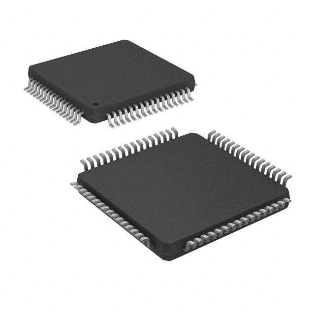


 工商网监
湘ICP备2023018690号
工商网监
湘ICP备2023018690号
