PIC16C712/716
8-Bit CMOS Microcontrollers with A/D Converter
and Capture/Compare/PWM
Devices included in this Data Sheet:
• PIC16C716
18-pin PDIP, SOIC, Windowed CERDIP
• High-performance RISC CPU
• Only 35 single-word instructions to learn
• All single-cycle instructions except for program
branches which are two cycle
• Operating speed: DC – 20 MHz clock input
DC – 200 ns instruction cycle
Device
Program
Memory
Data Memory
PIC16C712
1K
128
PIC16C716
2K
128
• Interrupt capability
(up to 7 internal/external interrupt sources)
• Eight-level deep hardware stack
• Direct, Indirect and Relative Addressing modes
• Power-on Reset (POR)
• Power-up Timer (PWRT) and
Oscillator Start-up Timer (OST)
• Watchdog Timer (WDT) with its own on-chip RC
oscillator for reliable operation
• Brown-out detection circuitry for
Brown-out Reset (BOR)
• Programmable code-protection
• Power-saving Sleep mode
• Selectable oscillator options
• Low-power, high-speed CMOS EPROM
technology
• Fully static design
• In-Circuit Serial Programming(ICSP™)
• Wide operating voltage range: 2.5V to 5.5V
• High Sink/Source Current 25/25 mA
• Commercial, Industrial and Extended temperature
ranges
• Low-power consumption:
- < 2 mA @ 5V, 4 MHz
- 22.5 A, typical @ 3V, 32 kHz
- < 1 A, typical standby current
1999-2013 Microchip Technology Inc.
RA2/AN2
RA3/AN3/VREF
1
18
2
17
RA4/T0CKI
MCLR/VPP
VSS
RB0/INT
RB1/T1OSO/T1CKI
RB2/T1OSI
RB3/CCP1
3
16
4
5
6
7
8
PIC16C716
PIC16C712
Microcontroller Core Features:
15
14
13
12
11
9
10
1
20
2
19
3
18
RA1/AN1
RA0/AN0
OSC1/CLKIN
OSC2/CLKOUT
VDD
RB7
RB6
RB5
RB4
20-pin SSOP
RA2/AN2
RA3/AN3/VREF
RA4/T0CKI
MCLR/VPP
VSS
VSS
RB0/INT
RB1/T1OSO/T1CKI
RB2/T1OSI
RB3/CCP1
4
5
6
7
8
PIC16C716
PIC16C712
• PIC16C712
Pin Diagrams
17
16
15
14
13
9
12
10
11
RA1/AN1
RA0/AN0
OSC1/CLKIN
OSC2/CLKOUT
VDD
VDD
RB7
RB6
RB5
RB4
Peripheral Features:
• Timer0: 8-bit timer/counter with 8-bit prescaler
• Timer1: 16-bit timer/counter with prescaler
can be incremented during Sleep via external
crystal/clock
• Timer2: 8-bit timer/counter with 8-bit period
register, prescaler and postscaler
• Capture, Compare, PWM module
• Capture is 16-bit, max. resolution is 12.5 ns,
Compare is 16-bit, max. resolution is 200 ns,
PWM maximum resolution is 10-bit
• 8-bit multi-channel Analog-to-Digital converter
DS41106C-page 1
�PIC16C712/716
Key Features
PIC® Mid-Range Reference Manual (DS33023)
PIC16C712
PIC16C716
Operating Frequency
DC – 20 MHz
DC – 20 MHz
Resets (and Delays)
POR, BOR (PWRT, OST)
POR, BOR (PWRT, OST)
Program Memory (14-bit words)
1K
2K
Data Memory (bytes)
128
128
Interrupts
7
7
I/O Ports
Ports A,B
Ports A,B
Timers
3
3
Capture/Compare/PWM modules
1
1
8-bit Analog-to-Digital Module
4 input channels
4 input channels
PIC16C7XX FAMILY OF DEVICES
Clock
Memory
PIC16C710
PIC16C71
PIC16C711
PIC16C712
PIC16C715
PIC16C716
Maximum Frequency
of Operation (MHz)
20
20
20
20
20
20
20
20
EPROM Program
Memory
(x14 words)
512
1K
1K
1K
2K
2K
2K
4K
Data Memory (bytes)
Timer Module(s)
Capture/Compare/
Peripherals PWM Module(s)
Serial Port(s)
(SPI™/I2C™, USART)
A/D Converter (8-bit)
Channels
36
36
68
128
128
128
128
192
TMR0
TMR0
TMR0
TMR0
TMR1
TMR2
TMR0
TMR0
TMR1
TMR2
TMR0
TMR1
TMR2
TMR0
TMR1
TMR2
—
—
—
1
—
1
1
2
—
—
—
—
—
—
SPI/I2C
SPI/I2C,
USART
4
4
4
4
4
4
5
5
Interrupt Sources
4
4
4
7
4
7
8
11
I/O Pins
13
13
13
13
13
13
22
22
2.5-6.0
3.0-6.0
2.5-6.0
2.5-5.5
2.5-5.5
2.5-5.5
2.5-5.5
2.5-5.5
Yes
Yes
Yes
Yes
Yes
Yes
Yes
Yes
Yes
—
Yes
Yes
Yes
Yes
Yes
Yes
Voltage Range (Volts)
Features
PIC16C72A PIC16C73B
In-Circuit Serial
Programming™
Brown-out Reset
Packages
DS41106C-page 2
18-pin DIP, 18-pin DIP, 18-pin DIP, 18-pin DIP, 18-pin DIP, 18-pin DIP, 28-pin SDIP, 28-pin SDIP,
SOIC;
SOIC
SOIC;
SOIC;
SOIC;
SOIC;
SOIC, SSOP SOIC
20-pin SSOP
20-pin SSOP 20-pin SSOP 20-pin SSOP 20-pin SSOP
1999-2013 Microchip Technology Inc.
�PIC16C712/716
Table of Contents
1.0 Device Overview .......................................................................................................................................................................... 5
2.0 Memory Organization ................................................................................................................................................................... 9
3.0 I/O Ports ..................................................................................................................................................................................... 21
4.0 Timer0 Module ........................................................................................................................................................................... 29
5.0 Timer1 Module ........................................................................................................................................................................... 31
6.0 Timer2 Module ........................................................................................................................................................................... 36
7.0 Capture/Compare/PWM (CCP) Module(s) ................................................................................................................................. 39
8.0 Analog-to-Digital Converter (A/D) Module.................................................................................................................................. 45
9.0 Special Features of the CPU...................................................................................................................................................... 51
10.0 Instruction Set Summary ............................................................................................................................................................ 67
11.0 Development Support................................................................................................................................................................. 69
12.0 Electrical Characteristics ............................................................................................................................................................ 73
13.0 Packaging Information................................................................................................................................................................ 89
Revision History .................................................................................................................................................................................. 95
Conversion Considerations ................................................................................................................................................................. 95
Migration from Base-line to Mid-Range Devices ................................................................................................................................. 95
Index ................................................................................................................................................................................................... 97
On-Line Support................................................................................................................................................................................. 101
Reader Response .............................................................................................................................................................................. 102
PIC16C712/716 Product Identification System .................................................................................................................................. 103
TO OUR VALUED CUSTOMERS
It is our intention to provide our valued customers with the best documentation possible to ensure successful use of your Microchip
products. To this end, we will continue to improve our publications to better suit your needs. Our publications will be refined and
enhanced as new volumes and updates are introduced.
If you have any questions or comments regarding this publication, please contact the Marketing Communications Department via
E-mail at docerrors@microchip.com or fax the Reader Response Form in the back of this data sheet to (480) 792-4150. We
welcome your feedback.
Most Current Data Sheet
To obtain the most up-to-date version of this data sheet, please register at our Worldwide Web site at:
http://www.microchip.com
You can determine the version of a data sheet by examining its literature number found on the bottom outside corner of any page.
The last character of the literature number is the version number, (e.g., DS30000A is version A of document DS30000).
Errata
An errata sheet, describing minor operational differences from the data sheet and recommended workarounds, may exist for current
devices. As device/documentation issues become known to us, we will publish an errata sheet. The errata will specify the revision
of silicon and revision of document to which it applies.
To determine if an errata sheet exists for a particular device, please check with one of the following:
• Microchip’s Worldwide Web site; http://www.microchip.com
• Your local Microchip sales office (see last page)
When contacting a sales office, please specify which device, revision of silicon and data sheet (include literature number) you are
using.
Customer Notification System
Register on our web site at www.microchip.com to receive the most current information on all of our products.
1999-2013 Microchip Technology Inc.
DS41106C-page 3
�PIC16C712/716
NOTES:
DS41106C-page 4
1999-2013 Microchip Technology Inc.
�PIC16C712/716
1.0
DEVICE OVERVIEW
There are two devices (PIC16C712, PIC16C716)
covered by this data sheet.
This document contains device-specific information.
Additional information may be found in the PIC® MidRange Reference Manual, (DS33023), which may be
obtained from your local Microchip Sales Representative or downloaded from the Microchip web site. The
Reference Manual should be considered a complementary document to this data sheet, and is highly recommended reading for a better understanding of the
device architecture and operation of the peripheral
modules.
FIGURE 1-1:
Figure 1-1 is the block diagram for both devices. The
pinouts are listed in Table 1-1.
PIC16C712/716 BLOCK DIAGRAM
13
EPROM
1K X 14
or
2K x 14
Program
Memory
Program
Bus
RAM Addr(1)
RA0/AN0
RA1/AN1
RA2/AN2
RA3/AN3/VREF
RA4/T0CKI
PORTB
9
Addr MUX
Instruction Reg
Direct Addr
7
8
Indirect
Addr
FSR Reg
STATUS Reg
8
3
OSC1/CLKIN
OSC2/CLKOUT
Timing
Generation
Oscillator
Start-up Timer
Power-on
Reset
Timer0
ALU
8
Watchdog
Timer
Brown-out
Reset
MCLR
Timer1
RB0/INT
RB1/T1OSO/T1CKI
RB2/T1OSI
RB3/CCP1
RB4
RB5
RB6
RB7
MUX
Power-up
Timer
Instruction
Decode &
Control
PORTA
RAM
128 x 8
File
Registers
8 Level Stack
(13-bit)
14
8
Data Bus
Program Counter
W Reg
VDD, VSS
Timer2
CCP1
A/D
Note 1: Higher order bits are from the STATUS register.
1999-2013 Microchip Technology Inc.
DS41106C-page 5
�PIC16C712/716
TABLE 1-1:
Pin
Name
MCLR/VPP
MCLR
PIC16C712/716 PINOUT DESCRIPTION
PIC16C712/716
DIP, SOIC
SSOP
4
4
16
Type
Type
I
ST
Master clear (Reset) input. This pin is
an active low Reset to the device.
Programming voltage input
I
ST
I
CMOS
Oscillator crystal input or external clock
source input. ST buffer when configured in RC mode. CMOS otherwise.
External clock source input.
15
O
—
O
—
Description
18
CLKIN
OSC2/CLKOUT
OSC2
Buffer
P
VPP
OSC1/CLKIN
OSC1
Pin
17
CLKOUT
Oscillator crystal output. Connects to
crystal or resonator in crystal oscillator
mode.
In RC mode, OSC2 pin outputs
CLKOUT which has 1/4 the frequency
of OSC1, and denotes the instruction
cycle rate.
PORTA is a bidirectional I/O port.
RA0/AN0
RA0
AN0
17
RA1/AN1
RA1
AN1
18
RA2/AN2
RA2
AN2
1
RA3/AN3/VREF
RA3
AN3
VREF
2
RA4/T0CKI
RA4
3
T0CKI
19
I/O
I
TTL
Analog
Digital I/O
Analog input 0
I/O
I
TTL
Analog
Digital I/O
Analog input 1
I/O
I
TTL
Analog
Digital I/O
Analog input 2
I/O
I
I
TTL
Analog
Analog
Digital I/O
Analog input 3
A/D Reference Voltage input.
I/O
ST/OD
I
ST
Digital I/O. Open drain when configured
as output.
Timer0 external clock input
20
1
2
3
Legend: TTL = TTL-compatible input
CMOS = CMOS compatible input or output
ST = Schmitt Trigger input with CMOS levels
OD = Open drain output
SM = SMBus compatible input. An external resistor is required if this pin is used as an output
NPU = N-channel pull-up
PU = Weak internal pull-up
No-P diode = No P-diode to VDD AN = Analog input or output
I = input
O = output
P = Power
L = LCD Driver
DS41106C-page 6
1999-2013 Microchip Technology Inc.
�PIC16C712/716
TABLE 1-1:
PIC16C712/716 PINOUT DESCRIPTION (CONTINUED)
Pin
Name
PIC16C712/716
DIP, SOIC
SSOP
Pin
Buffer
Type
Type
Description
PORTB is a bidirectional I/O port. PORTB
can be software programmed for internal
weak pull-ups on all inputs.
RB0/INT
RB0
INT
6
RB1/T1OSO/T1CKI
RB1
T1OSO
7
7
I/O
I
TTL
ST
Digital I/O
External Interrupt
I/O
O
TTL
—
I
ST
Digital I/O
Timer1 oscillator output. Connects to
crystal in oscillator mode.
Timer1 external clock input.
I/O
I
TTL
—
Digital I/O
Timer1 oscillator input. Connects to
crystal in oscillator mode.
I/O
I/O
TTL
ST
Digital I/O
Capture1 input, Compare1 output,
PWM1 output.
8
T1CKI
RB2/T1OSI
RB2
T1OSI
8
RB3/CCP1
RB3
CCP1
9
RB4
10
12
I/O
TTL
Digital I/O
Interrupt on change pin.
RB5
11
12
I/O
TTL
Digital I/O
Interrupt on change pin.
RB6
12
13
I/O
TTL
I
ST
Digital I/O
Interrupt on change pin.
ICSP programming clock.
RB7
13
14
I/O
TTL
I/O
ST
VSS
5
5, 6
P
—
Ground reference for logic and I/O pins.
VDD
14
15, 16
P
—
Positive supply for logic and I/O pins.
9
10
Digital I/O
Interrupt on change pin.
ICSP programming data.
Legend: TTL = TTL-compatible input
CMOS = CMOS compatible input or output
ST = Schmitt Trigger input with CMOS levels
OD = Open drain output
SM = SMBus compatible input. An external resistor is required if this pin is used as an output
NPU = N-channel pull-up
PU = Weak internal pull-up
No-P diode = No P-diode to VDD AN = Analog input or output
I = input
O = output
P = Power
L = LCD Driver
1999-2013 Microchip Technology Inc.
DS41106C-page 7
�PIC16C712/716
NOTES:
DS41106C-page 8
1999-2013 Microchip Technology Inc.
�PIC16C712/716
2.0
MEMORY ORGANIZATION
There are two memory blocks in each of these PIC®
microcontroller devices. Each block (Program Memory
and Data Memory) has its own bus so that concurrent
access can occur.
FIGURE 2-2:
PC
CALL, RETURN
RETFIE, RETLW
Additional information on device memory may be found
in the PIC® Mid-Range Reference Manual, (DS33023).
2.1
PROGRAM MEMORY MAP
AND STACK OF PIC16C716
13
Stack Level 1
Program Memory Organization
The PIC16C712/716 has a 13-bit Program Counter
(PC) capable of addressing an 8K x 14 program memory space. PIC16C712 has 1K x 14 words of program
memory and PIC16C716 has 2K x 14 words of program
memory. Accessing a location above the physically
implemented address will cause a wraparound.
FIGURE 2-1:
PROGRAM MEMORY MAP
AND STACK OF THE
PIC16C712
PC
CALL, RETURN
RETFIE, RETLW
User Memory
Space
The Reset vector is at 0000h and the interrupt vector is
at 0004h.
Stack Level 8
Reset Vector
0000h
Interrupt Vector
0004h
0005h
On-chip Program
Memory
07FFh
13
0800h
Stack Level 1
1FFFh
User Memory
Space
Stack Level 8
Reset Vector
0000h
Interrupt Vector
0004h
0005h
On-chip Program
Memory
03FFh
0400h
1FFFh
1999-2013 Microchip Technology Inc.
DS41106C-page 9
�PIC16C712/716
2.2
Data Memory Organization
The data memory is partitioned into multiple banks
which contain the General Purpose Registers and the
Special Function Registers. Bits RP1 and RP0 are the
bank select bits.
RP1(1)
RP0
(STATUS)
= 00 Bank 0
= 01 Bank 1
= 10 Bank 2 (not implemented)
= 11 Bank 3 (not implemented)
Note 1: Maintain this bit clear to ensure upward
compatibility with future products.
Each bank extends up to 7Fh (128 bytes). The lower
locations of each bank are reserved for the Special
Function Registers. Above the Special Function Registers are General Purpose Registers, implemented as
static RAM. All implemented banks contain Special
Function Registers. Some “high use” Special Function
Registers from one bank may be mirrored in another
bank for code reduction and quicker access.
2.2.1
GENERAL PURPOSE REGISTER
FILE
The register file can be accessed either directly, or
indirectly through the File Select Register FSR (see
Section 2.5 “Indirect Addressing, INDF and FSR
Registers”).
FIGURE 2-3:
REGISTER FILE MAP
File
Address
File
Address
00h
INDF(1)
INDF(1)
80h
01h
TMR0
OPTION_REG
81h
02h
PCL
PCL
82h
03h
STATUS
STATUS
83h
04h
FSR
FSR
84h
05h
PORTA
TRISA
85h
06h
PORTB
TRISB
86h
07h
DATACCP
TRISCCP
87h
88h
08h
89h
09h
0Ah
PCLATH
PCLATH
8Ah
0Bh
INTCON
INTCON
8Bh
0Ch
PIR1
PIE1
8Ch
0Eh
TMR1L
PCON
8Eh
0Fh
TMR1H
8Fh
10h
T1CON
90h
11h
TMR2
12h
T2CON
8Dh
0Dh
91h
PR2
92h
93h
13h
14h
94h
15h
CCPR1L
95h
16h
CCPR1H
96h
17h
CCP1CON
97h
18h
98h
19h
99h
1Ah
9Ah
1Bh
9Bh
1Ch
9Ch
9Dh
1Dh
1Eh
ADRES
1Fh
ADCON0
20h
General
Purpose
Registers
96 Bytes
9Eh
ADCON1
9Fh
General
Purpose
Registers
32 Bytes
A0h
BFh
C0h
7Fh
FFh
Bank 0
Bank 1
Unimplemented data memory locations,
read as ‘0’.
Note 1: Not a physical register.
DS41106C-page 10
1999-2013 Microchip Technology Inc.
�PIC16C712/716
2.2.2
SPECIAL FUNCTION REGISTERS
The Special Function Registers can be classified into
two sets; core (CPU) and peripheral. Those registers
associated with the core functions are described in
detail in this section. Those related to the operation of
the peripheral features are described in detail in that
peripheral feature section.
The Special Function Registers are registers used by
the CPU and Peripheral Modules for controlling the
desired operation of the device. These registers are
implemented as static RAM. A list of these registers is
give in Table 2-1.
TABLE 2-1:
Addr
SPECIAL FUNCTION REGISTER SUMMARY
Name
Bit 7
Bit 6
Bit 5
Bit 4
Bit 3
Bit 2
Bit 1
Bit 0
Value on: Value on
POR,
all other
BOR
Resets (4)
Bank 0
INDF(1)
Addressing this location uses contents of FSR to address data memory (not a physical register)
0000 0000 0000 0000
01h
TMR0
Timer0 Module’s Register
xxxx xxxx uuuu uuuu
02h
PCL(1)
Program Counter’s (PC) Least Significant Byte
0000 0000 0000 0000
00h
(1)
03h
STATUS
04h
FSR(1)
05h
PORTA(5,6)
06h
(5,6)
07h
PORTB
(4)
RP1
RP0
TO
PD
Z
DC
C
Indirect Data Memory Address Pointer
DATACCP
08h-09h
IRP
(4)
—
—
—(7)
—
PORTA Data Latch when written: PORTA pins when read
PORTB Data Latch when written: PORTB pins when read
(7)
—(7)
(7)
—
(7)
—
—
—
0Ah
PCLATH
0Bh
INTCON(1)
0Ch
PIR1
--xx xxxx --xu uuuu
xxxx xxxx uuuu uuuu
(7)
DCCP
(7)
—
DT1CK
Unimplemented
(1,2)
rr01 1xxx rr0q quuu
xxxx xxxx uuuu uuuu
xxxx xxxx xxxx xuxu
—
Write Buffer for the upper 5 bits of the Program Counter
—
—
—
—
GIE
PEIE
T0IE
INTE
RBIE
T0IF
INTF
RBIF
0000 000x 0000 000u
—
ADIF
—
—
—
CCP1IF
TMR2IF
TMR1IF
-0-- 0000 -0-- 0000
0Dh
—
0Eh
TMR1L
Holding Register for the Least Significant Byte of the 16-bit TMR1 Register
xxxx xxxx uuuu uuuu
0Fh
TMR1H
Holding Register for the Most Significant Byte of the 16-bit TMR1 Register
xxxx xxxx uuuu uuuu
10h
T1CON
11h
TMR2
12h
T2CON
Unimplemented
---0 0000 ---0 0000
—
—
—
T1CKPS1
T1CKPS0
T1OSCEN
T1SYNC
TMR1CS
TMR1ON
Timer2 Module’s Register
—
—
--00 0000 --uu uuuu
0000 0000 0000 0000
TOUTPS3 TOUTPS2
TOUTPS1
TOUTPS0
TMR2ON
T2CKPS1
T2CKPS0
-000 0000 -000 0000
13h-14h
15h
CCPR1L
Capture/Compare/PWM Register1 (LSB)
xxxx xxxx uuuu uuuu
16h
CCPR1H
Capture/Compare/PWM Register1 (MSB)
xxxx xxxx uuuu uuuu
17h
CCP1CON
18h-1Dh
—
1Eh
ADRES
1Fh
ADCON0
—
—
DC1B1
DC1B0
CCP1M3
CCP1M2
CCP1M1
CCP1M0
Unimplemented
—
A/D Result Register
ADCS1
ADCS0
--00 0000 --00 0000
—
xxxx xxxx uuuu uuuu
CHS2
CHS1
CHS0
GO/DONE
—
ADON
0000 00-0 0000 00-0
Legend: x = unknown, u = unchanged, q = value depends on condition, — = unimplemented, read as ‘0’,
Shaded locations are unimplemented, read as ‘0’.
Note 1: These registers can be addressed from either bank.
2: The upper byte of the program counter is not directly accessible. PCLATH is a holding register for PC whose contents
are transferred to the upper byte of the program counter.
3: Other (non Power-up) Resets include: external Reset through MCLR and the Watchdog Timer Reset.
4: The IRP and RP1 bits are reserved. Always maintain these bits clear.
5: On any device Reset, these pins are configured as inputs.
6: This is the value that will be in the port output latch.
7: Reserved bits; Do Not Use.
1999-2013 Microchip Technology Inc.
DS41106C-page 11
�PIC16C712/716
TABLE 2-1:
Addr
SPECIAL FUNCTION REGISTER SUMMARY (CONTINUED)
Name
Bit 7
Bit 6
Bit 5
Bit 4
Bit 3
Bit 2
Bit 1
Bit 0
Value on: Value on
POR,
all other
BOR
Resets (4)
Bank 1
80h
INDF(1)
81h
OPTION_
REG
82h
PCL(1)
83h
STATUS(1)
84h
FSR
(1)
85h
TRISA
86h
TRISB
87h
TRISCCP
88h-89h
—
8Ah
PCLATH(1,2)
8Bh
INTCON(1)
8Ch
PIE1
8Dh
—
8Eh
PCON
8Fh-91h
92h
93h-9Eh
9Fh
—
PR2
Addressing this location uses contents of FSR to address data memory (not a physical register)
RBPU
INTEDG
T0CS
T0SE
PSA
PS2
PS1
PS0
PD
Z
DC
C
Program Counter’s (PC) Least Significant Byte
IRP(4)
RP1(4)
RP0
TO
—
—(7)
—
rr01 1xxx rr0q quuu
xxxx xxxx uuuu uuuu
PORTA Data Direction Register
--x1 1111 --x1 1111
PORTB Data Direction Register
1111 1111 1111 1111
—(7)
—(7)
—
—
GIE
PEIE
T0IE
INTE
RBIE
T0IF
INTF
RBIF
0000 000x 0000 000u
—
ADIE
—
—
—
CCP1IE
TMR2IE
TMR1IE
-0-- -000 -0-- -000
—
—
—
—
POR
BOR
---- --qq ---- --uu
—(7)
—(7)
—(7)
TCCP
—(7)
TT1CK
Unimplemented
—
Unimplemented
—
—
—
—
1111 1111 1111 1111
Unimplemented
—
—
---0 0000 ---0 0000
—
—
Unimplemented
—
xxxx x1x1 xxxx x1x1
—
Write Buffer for the upper 5 bits of the Program Counter
Timer2 Period Register
ADCON1
1111 1111 1111 1111
0000 0000 0000 0000
Indirect Data Memory Address Pointer
—
0000 0000 0000 0000
—
—
—
PCFG2
PCFG1
PCFG0
—
—
---- -000
---- -000
Legend: x = unknown, u = unchanged, q = value depends on condition, — = unimplemented, read as ‘0’,
Shaded locations are unimplemented, read as ‘0’.
Note 1: These registers can be addressed from either bank.
2: The upper byte of the program counter is not directly accessible. PCLATH is a holding register for PC whose contents
are transferred to the upper byte of the program counter.
3: Other (non Power-up) Resets include: external Reset through MCLR and the Watchdog Timer Reset.
4: The IRP and RP1 bits are reserved. Always maintain these bits clear.
5: On any device Reset, these pins are configured as inputs.
6: This is the value that will be in the port output latch.
7: Reserved bits; Do Not Use.
DS41106C-page 12
1999-2013 Microchip Technology Inc.
�PIC16C712/716
2.2.2.1
Status Register
It is recommended, therefore, that only BCF, BSF,
SWAPF and MOVWF instructions are used to alter the
STATUS register because these instructions do not
affect the Z, C or DC bits from the STATUS register. For
other instructions, not affecting any Status bits, see the
“Instruction Set Summary.”
The STATUS register, shown in Figure 2-4, contains
the arithmetic status of the ALU, the Reset status and
the bank select bits for data memory.
The STATUS register can be the destination for any
instruction, as with any other register. If the STATUS
register is the destination for an instruction that affects
the Z, DC or C bits, then the write to these three bits is
disabled. These bits are set or cleared according to the
device logic. Furthermore, the TO and PD bits are not
writable. Therefore, the result of an instruction with the
STATUS register as destination may be different than
intended.
Note 1: These devices do not use bits IRP and
RP1 (STATUS). Maintain these bits
clear to ensure upward compatibility with
future products.
2: The C and DC bits operate as a borrow
and digit borrow bit, respectively, in subtraction. See the SUBLW and SUBWF
instructions for examples.
For example, CLRF STATUS will clear the upper-three
bits and set the Z bit. This leaves the STATUS register
as 000u u1uu (where u = unchanged).
FIGURE 2-4:
R/W-0
IRP
R/W-0
RP1
STATUS REGISTER (ADDRESS 03h, 83h)
R/W-0
RP0
R-1
TO
R-1
PD
R/W-x
Z
R/W-x
DC
R/W-x
C
bit7
bit 7:
bit0
R = Readable bit
W = Writable bit
U = Unimplemented bit,
read as ‘0’
-n = Value at POR Reset
IRP: Register Bank Select bit (used for indirect addressing)
1 = Bank 2, 3 (100h-1FFh) – not implemented, maintain clear
0 = Bank 0, 1 (00h-FFh) – not implemented, maintain clear
bit 6-5: RP1:RP0: Register Bank Select bits (used for direct addressing)
01 = Bank 1 (80h-FFh)
00 = Bank 0 (00h-7Fh)
Each bank is 128 bytes
Note: RP1 = not implemented, maintain clear
bit 4:
TO: Time-out bit
1 = After power-up, CLRWDT instruction, or SLEEP instruction
0 = A WDT Time-out occurred
bit 3:
PD: Power-down bit
1 = After power-up or by the CLRWDT instruction
0 = By execution of the SLEEP instruction
bit 2:
Z: Zero bit
1 = The result of an arithmetic or logic operation is zero
0 = The result of an arithmetic or logic operation is not zero
bit 1:
DC: Digit carry/borrow bit (ADDWF, ADDLW,SUBLW,SUBWF instructions) (for borrow the polarity is reversed)
1 = A carry-out from the 4th low order bit of the result occurred
0 = No carry-out from the 4th low order bit of the result
bit 0:
C: Carry/borrow bit (ADDWF, ADDLW,SUBLW,SUBWF instructions)
1 = A carry-out from the most significant bit of the result occurred
0 = No carry-out from the most significant bit of the result occurred
Note: For borrow the polarity is reversed. A subtraction is executed by adding the two’s complement of the
second operand. For rotate (RRF, RLF) instructions, this bit is loaded with either the high or low order bit of
the source register.
1999-2013 Microchip Technology Inc.
DS41106C-page 13
�PIC16C712/716
2.2.2.2
OPTION_REG Register
Note:
The OPTION_REG register is a readable and writable
register, which contains various control bits to configure
the TMR0 prescaler/WDT postscaler (single assignable register known also as the prescaler), the External
INT Interrupt, TMR0 and the weak pull-ups on PORTB.
FIGURE 2-5:
To achieve a 1:1 prescaler assignment for
the TMR0 register, assign the prescaler to
the Watchdog Timer.
OPTION_REG REGISTER (ADDRESS 81h)
R/W-1
R/W-1
R/W-1
R/W-1
R/W-1
R/W-1
R/W-1
R/W-1
RBPU
INTEDG
T0CS
T0SE
PSA
PS2
PS1
PS0
bit7
bit0
bit 7:
RBPU: PORTB Pull-up Enable bit
1 = PORTB pull-ups are disabled
0 = PORTB pull-ups are enabled by individual port latch values
bit 6:
INTEDG: Interrupt Edge Select bit
1 = Interrupt on rising edge of RB0/INT pin
0 = Interrupt on falling edge of RB0/INT pin
bit 5:
T0CS: TMR0 Clock Source Select bit
1 = Transition on RA4/T0CKI pin
0 = Internal instruction cycle clock (CLKOUT)
bit 4:
T0SE: TMR0 Source Edge Select bit
1 = Increment on high-to-low transition on RA4/T0CKI pin
0 = Increment on low-to-high transition on RA4/T0CKI pin
bit 3:
PSA: Prescaler Assignment bit
1 = Prescaler is assigned to the WDT
0 = Prescaler is assigned to the Timer0 module
R = Readable bit
W = Writable bit
U = Unimplemented bit,
read as ‘0’
- n = Value at POR Reset
bit 2-0: PS2:PS0: Prescaler Rate Select bits
Bit Value
000
001
010
011
100
101
110
111
DS41106C-page 14
TMR0 Rate
1:2
1:4
1:8
1 : 16
1 : 32
1 : 64
1 : 128
1 : 256
WDT Rate
1:1
1:2
1:4
1:8
1 : 16
1 : 32
1 : 64
1 : 128
1999-2013 Microchip Technology Inc.
�PIC16C712/716
2.2.2.3
INTCON Register
Note:
The INTCON Register is a readable and writable register which contains various enable and flag bits for the
TMR0 register overflow, RB Port change and External
RB0/INT pin interrupts.
FIGURE 2-6:
Interrupt flag bits get set when an interrupt
condition occurs, regardless of the state of
its corresponding enable bit or the global
enable bit, GIE (INTCON). User software should ensure the appropriate interrupt flag bits are clear prior to enabling an
interrupt.
INTCON REGISTER (ADDRESS 0Bh, 8Bh)
R/W-0
R/W-0
R/W-0
R/W-0
R/W-0
R/W-0
R/W-0
R/W-x
GIE
PEIE
T0IE
INTE
RBIE
T0IF
INTF
RBIF
bit7
bit0
R = Readable bit
W = Writable bit
U = Unimplemented bit,
read as ‘0’
-n = Value at POR Reset
bit 7:
GIE: Global Interrupt Enable bit
1 = Enables all unmasked interrupts
0 = Disables all interrupts
bit 6:
PEIE: Peripheral Interrupt Enable bit
1 = Enables all unmasked peripheral interrupts
0 = Disables all peripheral interrupts
bit 5:
T0IE: TMR0 Overflow Interrupt Enable bit
1 = Enables the TMR0 interrupt
0 = Disables the TMR0 interrupt
bit 4:
IINTE: RB0/INT External Interrupt Enable bit
1 = Enables the RB0/INT external interrupt
0 = Disables the RB0/INT external interrupt
bit 3:
RBIE: RB Port Change Interrupt Enable bit
1 = Enables the RB port change interrupt
0 = Disables the RB port change interrupt
bit 2:
T0IF: TMR0 Overflow Interrupt Flag bit
1 = TMR0 register has overflowed (must be cleared in software)
0 = TMR0 register did not overflow
bit 1:
INTF: RB0/INT External Interrupt Flag bit
1 = The RB0/INT external interrupt occurred (must be cleared in software)
0 = The RB0/INT external interrupt did not occur
bit 0:
RBIF: RB Port Change Interrupt Flag bit
1 = At least one of the RB7:RB4 pins changed state (must be cleared in software)
0 = None of the RB7:RB4 pins have changed state
1999-2013 Microchip Technology Inc.
DS41106C-page 15
�PIC16C712/716
2.2.2.4
PIE1 Register
Note:
This register contains the individual enable bits for the
peripheral interrupts.
FIGURE 2-7:
Bit PEIE (INTCON) must be set to
enable any peripheral interrupt.
PIE1 REGISTER (ADDRESS 8Ch)
U-0
R/W-0
U-0
U-0
R/W-0
R/W-0
R/W-0
R/W-0
—
ADIE
—
—
—
CCP1IE
TMR2IE
TMR1IE
bit7
bit0
bit 7:
Unimplemented: Read as ‘0’
bit 6:
ADIE: A/D Converter Interrupt Enable bit
1 = Enables the A/D interrupt
0 = Disables the A/D interrupt
R = Readable bit
W = Writable bit
U = Unimplemented bit,
read as ‘0’
-n = Value at POR Reset
bit 5-3: Unimplemented: Read as ‘0’
bit 2:
CCP1IE: CCP1 Interrupt Enable bit
1 = Enables the CCP1 interrupt
0 = Disables the CCP1 interrupt
bit 1:
TMR2IE: TMR2 to PR2 Match Interrupt Enable bit
1 = Enables the TMR2 to PR2 match interrupt
0 = Disables the TMR2 to PR2 match interrupt
bit 0:
TMR1IE: TMR1 Overflow Interrupt Enable bit
1 = Enables the TMR1 overflow interrupt
0 = Disables the TMR1 overflow interrupt
DS41106C-page 16
1999-2013 Microchip Technology Inc.
�PIC16C712/716
2.2.2.5
PIR1 Register
Note:
This register contains the individual flag bits for the
peripheral interrupts.
FIGURE 2-8:
Interrupt flag bits get set when an interrupt
condition occurs, regardless of the state of
its corresponding enable bit or the global
enable bit, GIE (INTCON). User software should ensure the appropriate interrupt flag bits are clear prior to enabling an
interrupt.
PIR1 REGISTER (ADDRESS 0Ch)
U-0
R/W-0
U-0
U-0
R/W-0
R/W-0
R/W-0
R/W-0
—
ADIF
—
—
—
CCP1IF
TMR2IF
TMR1IF
bit7
bit0
bit 7:
Unimplemented: Read as ‘0’
bit 6:
ADIF: A/D Converter Interrupt Flag bit
1 = An A/D conversion completed (must be cleared in software)
0 = The A/D conversion is not complete
R = Readable bit
W = Writable bit
U = Unimplemented bit,
read as ‘0’
-n = Value at POR Reset
bit 5-3: Unimplemented: Read as ‘0’
bit 2:
CCP1IF: CCP1 Interrupt Flag bit
Capture Mode:
1 = A TMR1 register capture occurred (must be cleared in software)
0 = No TMR1 register capture occurred
Compare Mode:
1 = A TMR1 register compare match occurred (must be cleared in software)
0 = No TMR1 register compare match occurred
PWM Mode:
Unused in this mode
bit 1:
TMR2IF: TMR2 to PR2 Match Interrupt Flag bit
1 = TMR2 to PR2 match occurred (must be cleared in software)
0 = No TMR2 to PR2 match occurred
bit 0:
TMR1IF: TMR1 Overflow Interrupt Flag bit
1 = TMR1 register overflowed (must be cleared in software)
0 = TMR1 register did not overflow
1999-2013 Microchip Technology Inc.
DS41106C-page 17
�PIC16C712/716
2.2.2.6
PCON Register
Note:
The Power Control (PCON) register contains a flag bit
to allow differentiation between a Power-on Reset
(POR) to an external MCLR Reset or WDT Reset.
These devices contain an additional bit to differentiate
a Brown-out Reset condition from a Power-on Reset
condition.
FIGURE 2-9:
If the BODEN Configuration bit is set, BOR
is ‘1’ on Power-on Reset. If the BODEN
Configuration bit is clear, BOR is unknown
on Power-on Reset.
The BOR Status bit is a “don’t care” and is
not necessarily predictable if the brown-out
circuit is disabled (the BODEN Configuration bit is clear). BOR must then be set by
the user and checked on subsequent
resets to see if it is clear, indicating a
brown-out has occurred.
PCON REGISTER (ADDRESS 8Eh)
U-0
U-0
U-0
U-0
U-0
U-0
R/W-0
R/W-q
—
—
—
—
—
—
POR
BOR
bit7
bit0
R = Readable bit
W = Writable bit
U = Unimplemented bit,
read as ‘0’
-n = Value at POR Reset
bit 7-2: Unimplemented: Read as ‘0’
bit 1:
POR: Power-on Reset Status bit
1 = No Power-on Reset occurred
0 = A Power-on Reset occurred (must be set in software after a Power-on Reset occurs)
bit 0:
BOR: Brown-out Reset Status bit
1 = No Brown-out Reset occurred
0 = A Brown-out Reset occurred (must be set in software after a Brown-out Reset occurs)
DS41106C-page 18
1999-2013 Microchip Technology Inc.
�PIC16C712/716
2.3
PCL and PCLATH
The Program Counter (PC) specifies the address of the
instruction to fetch for execution. The PC is 13 bits
wide. The low byte is called the PCL register. This register is readable and writable. The high byte is called
the PCH register. This register contains the PC
bits and is not directly readable or writable. All updates
to the PCH register go through the PCLATH register.
2.3.1
STACK
The stack allows a combination of up to 8 program calls
and interrupts to occur. The stack contains the return
address from this branch in program execution.
2.4
Program Memory Paging
The CALL and GOTO instructions provide 11 bits of
address to allow branching within any 2K program
memory page. When doing a CALL or GOTO instruction,
the upper bit of the address is provided by
PCLATH. When doing a CALL or GOTO instruction,
the user must ensure that the page select bit is programmed so that the desired program memory page is
addressed. If a return from a CALL instruction (or interrupt) is executed, the entire 13-bit PC is pushed onto
the stack. Therefore, manipulation of the PCLATH
bit is not required for the return instructions (which
POPs the address from the stack).
Mid-range devices have an 8-level deep x 13-bit wide
hardware stack. The stack space is not part of either
program or data space and the Stack Pointer is not
readable or writable. The PC is PUSHed onto the stack
when a CALL instruction is executed or an interrupt
causes a branch. The stack is POPed in the event of a
RETURN, RETLW or a RETFIE instruction execution.
PCLATH is not modified when the stack is PUSHed or
POPed.
After the stack has been PUSHed eight times, the ninth
push overwrites the value that was stored from the first
push. The tenth push overwrites the second push (and
so on).
1999-2013 Microchip Technology Inc.
DS41106C-page 19
�PIC16C712/716
2.5
EXAMPLE 2-2:
Indirect Addressing, INDF and
FSR Registers
The INDF register is not a physical register. Addressing
INDF actually addresses the register whose address is
contained in the FSR register (FSR is a pointer). This is
indirect addressing.
EXAMPLE 2-1:
HOW TO CLEAR RAM
USING INDIRECT
ADDRESSING
MOVLW
MOVWF
CLRF
INCF
BTFSS
GOTO
NEXT
INDIRECT ADDRESSING
0x20
FSR
INDF
FSR
FSR,4
NEXT
;initialize pointer
; to RAM
;clear INDF register
;inc pointer
;all done?
;NO, clear next
CONTINUE
•
•
•
•
Register file 05 contains the value 10h
Register file 06 contains the value 0Ah
Load the value 05 into the FSR register
A read of the INDF register will return the value of
10h
• Increment the value of the FSR register by one
(FSR = 06)
• A read of the INDR register now will return the
value of 0Ah.
:
;YES, continue
An effective 9-bit address is obtained by concatenating
the 8-bit FSR register and the IRP bit (STATUS), as
shown in Figure 2-10. However, IRP is not used in the
PIC16C712/716.
Reading INDF itself indirectly (FSR = 0) will produce
00h. Writing to the INDF register indirectly results in a
no-operation (although Status bits may be affected).
A simple program to clear RAM locations 20h-2Fh
using indirect addressing is shown in Example 2-2.
FIGURE 2-10:
DIRECT/INDIRECT ADDRESSING
Direct Addressing
RP1:RP0
6
Indirect Addressing
from opcode
0
IRP
FSR register
0
(2)
(2)
bank select
7
bank select
location select
00
00h
01
80h
10
100h
(3)
Data
Memory(1)
7Fh
Bank 0
FFh
Bank 1
17Fh
Bank 2
location select
11
180h
(3)
1FFh
Bank 3
Note 1: For register file map detail see Figure 2-3.
2: Maintain clear for upward compatibility with future products.
3: Not implemented.
DS41106C-page 20
1999-2013 Microchip Technology Inc.
�PIC16C712/716
3.0
I/O PORTS
Some pins for these I/O ports are multiplexed with an
alternate function for the peripheral features on the
device. In general, when a peripheral is enabled, that
pin may not be used as a general purpose I/O pin.
Additional information on I/O ports may be found in the
PIC® Mid-Range Reference Manual, (DS33023).
3.1
PORTA and the TRISA Register
PORTA is a 5-bit wide bidirectional port. The corresponding data direction register is TRISA. Setting a
TRISA bit (= 1) will make the corresponding PORTA pin
an input, (i.e., put the corresponding output driver in a
High-Impedance mode). Clearing a TRISA bit (= 0) will
make the corresponding PORTA pin an output, (i.e., put
the contents of the output latch on the selected pin).
Reading the PORTA register reads the status of the
pins whereas writing to it will write to the port latch. All
write operations are read-modify-write operations.
Therefore, a write to a port implies that the port pins are
read, the value is modified, and then written to the port
data latch.
1999-2013 Microchip Technology Inc.
Pin RA4 is multiplexed with the Timer0 module clock
input to become the RA4/T0CKI pin. The RA4/T0CKI
pin is a Schmitt Trigger input and an open drain output.
All other RA port pins have TTL input levels and full
CMOS output drivers.
PORTA pins, RA3:0, are multiplexed with analog
inputs and analog VREF input. The operation of each
pin is selected by clearing/setting the control bits in the
ADCON1 register (A/D Control Register1).
Note:
On a Power-on Reset, these pins are
configured as analog inputs and read as
‘0’.
The TRISA register controls the direction of the RA
pins, even when they are being used as analog inputs.
The user must ensure the bits in the TRISA register are
maintained set when using them as analog inputs.
EXAMPLE 3-1:
INITIALIZING PORTA
BCF
CLRF
STATUS, RP0
PORTA
BSF
MOVLW
STATUS, RP0
0xEF
MOVWF
TRISA
BCF
STATUS, RP0
;
;
;
;
;
;
;
;
;
;
Initialize PORTA by
clearing output
data latches
Select Bank 1
Value used to
initialize data
direction
Set RA as inputs
RA as outputs
; Return to Bank 0
DS41106C-page 21
�PIC16C712/716
FIGURE 3-1:
BLOCK DIAGRAM OF RA3:RA0
DATA
BUS
D
Q
VDD
VDD
WR
PORT
Q
CK
P
Data Latch
D
WR
TRIS
N
Q
VSS VSS
Analog
input
mode
Q
CK
I/O pin
TRIS Latch
TTL
Input
Buffer
RD TRIS
Q
D
EN
RD PORT
To A/D Converter
FIGURE 3-2:
BLOCK DIAGRAM OF RA4/T0CKI PIN
DATA
BUS
D
Q
WR
PORT
CK
Q
I/O Pin
N
Data Latch
D
WR
TRIS
Q
CK
VSS
VSS
Schmitt
Trigger
Input
Buffer
Q
TRIS Latch
RD TRIS
Q
D
ENEN
RD PORT
TMR0 Clock Input
DS41106C-page 22
1999-2013 Microchip Technology Inc.
�PIC16C712/716
TABLE 3-1:
PORTA FUNCTIONS
Name
Bit#
Buffer
RA0/AN0
RA1/AN1
RA2/AN2
RA3/AN3/VREF
bit 0
bit 1
bit 2
bit 3
TTL
TTL
TTL
TTL
Function
Input/output or analog input
Input/output or analog input
Input/output or analog input
Input/output or analog input or VREF
Input/output or external clock input for Timer0
RA4/T0CKI
bit 4
ST
Output is open drain type
Legend: TTL = TTL input, ST = Schmitt Trigger input
TABLE 3-2:
SUMMARY OF REGISTERS ASSOCIATED WITH PORTA
Bit 7 Bit 6 Bit 5 Bit 4 Bit 3
Bit 2
Bit 1
Bit 0
Value on
POR,
BOR
Value on all
other Resets
—
—(1)
RA2
RA1
RA0
--xx xxxx
--xu uuuu
—
—
—(1) PORTA Data Direction Register
--11 1111
--11 1111
—
—
---- -000
---- -000
Address
Name
05h
PORTA
—
85h
TRISA
9Fh
ADCON1
—
RA4
—
RA3
—
PCFG2 PCFG1 PCFG0
Legend: x = unknown, u = unchanged, — = unimplemented locations read as ‘0’. Shaded cells are not used by
PORTA.
Note 1: Reserved bits; Do Not Use.
1999-2013 Microchip Technology Inc.
DS41106C-page 23
�PIC16C712/716
3.2
PORTB and the TRISB Register
Each of the PORTB pins has a weak internal pull-up. A
single control bit can turn on all the pull-ups. This is performed by clearing bit RBPU (OPTION_REG). The
weak pull-up is automatically turned off when the port
pin is configured as an output. The pull-ups are
disabled on a Power-on Reset.
PORTB is an 8-bit wide bidirectional port. The corresponding data direction register is TRISB. Setting a
TRISB bit (= 1) will make the corresponding PORTB
pin an input, (i.e., put the corresponding output driver in
a High-Impedance mode). Clearing a TRISB bit (= 0)
will make the corresponding PORTB pin an output,
(i.e., put the contents of the output latch on the selected
pin).
EXAMPLE 3-2:
INITIALIZING PORTB
BCF
CLRF
STATUS, RP0
PORTB
BSF
MOVLW
STATUS, RP0
0xCF
MOVWF
TRISB
;
;
;
;
;
;
;
;
;
;
Initialize PORTB by
clearing output
data latches
Select Bank 1
Value used to
initialize data
direction
Set RB as inputs
RB as outputs
; RB as inputs
FIGURE 3-3:
BLOCK DIAGRAM OF RB0 PIN
VDD
RBPU(1)
DATA BUS
WR PORT
weak VDD
P pull-up
Data Latch
D
Q
I/O
pin
CK
TRIS Latch
D
Q
WR TRIS
TTL
Input
Buffer
CK
VSS
RD TRIS
Q
RD PORT
D
EN
RB0/INT
Schmitt Trigger
Buffer
Note 1:
DS41106C-page 24
RD PORT
To enable weak pull-ups, set the appropriate TRIS bit(s) and clear the RBPU bit (OPTION_REG).
1999-2013 Microchip Technology Inc.
�PIC16C712/716
PORTB pins RB3:RB1 are multiplexed with several
peripheral functions (Table 3-3). PORTB pins RB3:RB0
have Schmitt Trigger input buffers.
PORTB. The “mismatch” outputs of RB7:RB4 are
OR’ed together to generate the RB Port Change
Interrupt with flag bit RBIF (INTCON).
When enabling peripheral functions, care should be
taken in defining TRIS bits for each PORTB pin. Some
peripherals override the TRIS bit to make a pin an output, while other peripherals override the TRIS bit to
make a pin an input. Since the TRIS bit override is in
effect while the peripheral is enabled, read-modifywrite instructions (BSF, BCF, XORWF) with TRISB as
destination should be avoided. The user should refer to
the corresponding peripheral section for the correct
TRIS bit settings.
This interrupt can wake the device from Sleep. The
user, in the Interrupt Service Routine, can clear the
interrupt in the following manner:
Four of PORTB’s pins, RB7:RB4, have an interrupt-onchange feature. Only pins configured as inputs can
cause this interrupt to occur (i.e., any RB7:RB4 pin
configured as an output is excluded from the interrupton-change comparison). The input pins, RB7:RB4, are
compared with the old value latched on the last read of
The interrupt-on-change feature is recommended for
wake-up on key depression operation and operations
where PORTB is only used for the interrupt-on-change
feature. Polling of PORTB is not recommended while
using the interrupt-on-change feature.
FIGURE 3-4:
a)
b)
Any read or write of PORTB will end the
mismatch condition.
Clear flag bit RBIF.
A mismatch condition will continue to set flag bit RBIF.
Reading PORTB will end the mismatch condition and
allow flag bit RBIF to be cleared.
BLOCK DIAGRAM OF RB1/T1OSO/T1CKI PIN
RBPU(1)
T1OSCEN
T1CS
TMR1CS
1
Data Bus
RD
DATACCP
0
DATACCP
D
WR
DATACCP
CK
VDD
Q
Weak
P Pull-up
Q
VDD
TRISCCP
D
WR
TRISCCP
CK
1
Q
RB1/T1OSO/T1CKI
0
Q
PORTB
D
WR
PORTB
CK
1
Q
VSS
0
Q
TRISB
D
WR TRISB
CK
Q
Q
T1OSCEN
TMR1CS
1
TTL Buffer
RD PORTB
0
T1CLKIN
ST
Buffer
Note 1: To enable weak pull-ups, set the appropriate TRIS bit(s) and clear the RBPU bit (OPTION_REG).
1999-2013 Microchip Technology Inc.
DS41106C-page 25
�PIC16C712/716
FIGURE 3-5:
BLOCK DIAGRAM OF RB2/T1OSI PIN
VDD
RBPU(1)
weak
P pull-up
T1OSCEN
VDD
PORTB
DATA BUS
WR PORTB
D
Q
CK
RB1/T1OSO/T1CKI
Q
VSS
TRISB
D
WR TRISB
Q
CK
Q
T1OSCEN
RD PORTB
TTL Buffer
Note 1: To enable weak pull-ups, set the appropriate TRIS bit(s) and clear the RBPU bit (OPTION_REG).
FIGURE 3-6:
BLOCK DIAGRAM OF RB3/CCP1 PIN
RBPU(1)
CCPON
0
CCPON
DATACCP
D
WR
DATACCP
CK
CCPOUT
RD
DATACCP
CCPIN
1
DATA BUS
1
Q
0
VDD
Q
weak
P pull-up
VDD
TRISCCP
D
WR
TRISCCP
CK
Q
1
Q
RB3/CCP1
0
CCP
Output
Mode
PORTB
D
WR
PORTB
CK
Q
1
Q
0
VSS
TRISB
D
WR
TRISB
CK
Q
Q
CCPON
1
RD PORTB
0
TTL Buffer
Note 1: To enable weak pull-ups, set the appropriate TRIS bit(s) and clear the RBPU bit (OPTION_REG).
DS41106C-page 26
1999-2013 Microchip Technology Inc.
�PIC16C712/716
FIGURE 3-7:
BLOCK DIAGRAM OF RB7:RB4 PINS
VDD
RBPU(1)
DATA BUS
weak
P pull-up
VDD
Data Latch
D
Q
WR PORT
I/O
pin
CK
TRIS Latch
D
Q
WR TRIS
VSS
TTL
Buffer
CK
ST
Buffer
RD TRIS
Q
Latch
D
EN
RD PORT
Q1
Set RBIF
Q
From other
RB7:RB4 pins
D
RD PORT
EN
Q3
RB7:RB6 in Serial Programming mode
Note 1: To enable weak pull-ups, set the appropriate TRIS bit(s) and clear the RBPU bit (OPTION_REG).
TABLE 3-3:
Name
PORTB FUNCTIONS
Bit#
Buffer
Function
TTL/ST(1)
Input/output pin or external interrupt input. Internal software
programmable weak pull-up.
(1)
Input/output pin or Timer1 oscillator output, or Timer1 clock input. Internal
RB1/T1OS0/
bit 1
TTL/ST
software programmable weak pull-up. See Timer1 section for detailed
T1CKI
operation.
(1)
Input/output pin or Timer1 oscillator input. Internal software programmable
RB2/T1OSI
bit 2
TTL/ST
weak pull-up. See Timer1 section for detailed operation.
(1)
Input/output pin or Capture 1 input, or Compare 1 output, or PWM1 output.
RB3/CCP1
bit 3
TTL/ST
Internal software programmable weak pull-up. See CCP1 section for
detailed operation.
RB4
bit 4
TTL
Input/output pin (with interrupt-on-change). Internal software programmable
weak pull-up.
RB5
bit 5
TTL
Input/output pin (with interrupt-on-change). Internal software programmable
weak pull-up.
RB6
bit 6
TTL/ST(2)
Input/output pin (with interrupt-on-change). Internal software programmable
weak pull-up. Serial programming clock.
RB7
bit 7
TTL/ST(2)
Input/output pin (with interrupt-on-change). Internal software programmable
weak pull-up. Serial programming data.
Legend: TTL = TTL input, ST = Schmitt Trigger input
Note 1: This buffer is a Schmitt Trigger input when configured as the external interrupt or peripheral input.
2: This buffer is a Schmitt Trigger input when used in Serial Programming mode.
RB0/INT
bit 0
1999-2013 Microchip Technology Inc.
DS41106C-page 27
�PIC16C712/716
TABLE 3-4:
SUMMARY OF REGISTERS ASSOCIATED WITH PORTB
Address
Name
Bit 7
Bit 6
Bit 5
Bit 4
Bit 3
Bit 2
Bit 1
Bit 0
Value on:
POR,
BOR
Value on all
other Resets
06h
PORTB
RB7
RB6
RB5
RB4
RB3
RB2
RB1
RB0
xxxx xxxx
uuuu uuuu
86h
TRISB
1111 1111
1111 1111
81h
OPTION_REG
1111 1111
1111 1111
PORTB Data Direction Register
RBPU
INTEDG
T0CS
T0SE
PSA
PS2
PS1
PS0
Legend: x = unknown, u = unchanged. Shaded cells are not used by PORTB.
DS41106C-page 28
1999-2013 Microchip Technology Inc.
�PIC16C712/716
4.0
TIMER0 MODULE
Additional information on external clock requirements
is available in the PIC® Mid-Range Reference Manual,
(DS33023).
The Timer0 module timer/counter has the following
features:
•
•
•
•
•
•
4.2
8-bit timer/counter
Readable and writable
Internal or external clock select
Edge select for external clock
8-bit software programmable prescaler
Interrupt on overflow from FFh to 00h
An 8-bit counter is available as a prescaler for the
Timer0 module or as a postscaler for the Watchdog
Timer, respectively (Figure 4-2). For simplicity, this
counter is being referred to as “prescaler” throughout
this data sheet. Note that there is only one prescaler
available, which is mutually exclusively shared
between the Timer0 module and the Watchdog Timer.
Thus, a prescaler assignment for the Timer0 module
means that there is no prescaler for the Watchdog
Timer and vice-versa.
Figure 4-1 is a simplified block diagram of the Timer0
module.
Additional information on timer modules is available in
the PIC® Mid-Range Reference Manual, (DS33023).
4.1
The prescaler is not readable or writable.
Timer0 Operation
The PSA and PS2:PS0 bits (OPTION_REG)
determine the prescaler assignment and prescale ratio.
Timer0 can operate as a timer or as a counter.
Clearing bit PSA will assign the prescaler to the Timer0
module. When the prescaler is assigned to the Timer0
module, prescale values of 1:2, 1:4, ..., 1:256 are
selectable.
Timer mode is selected by clearing bit T0CS
(OPTION_REG). In timer mode, the Timer0 module will increment every instruction cycle (without prescaler). If the TMR0 register is written, the increment is
inhibited for the following two instruction cycles. The
user can work around this by writing an adjusted value
to the TMR0 register.
Setting bit PSA will assign the prescaler to the Watchdog Timer (WDT). When the prescaler is assigned to
the WDT, prescale values of 1:1, 1:2, ..., 1:128 are
selectable.
Counter mode is selected by setting bit T0CS
(OPTION_REG). In Counter mode, Timer0 will
increment on every rising or falling edge of pin RA4/
T0CKI. The incrementing edge is determined by the
Timer0
Source
Edge
Select
bit
T0SE
(OPTION_REG). Clearing bit T0SE selects the
rising edge. Restrictions on the external clock input are
discussed below.
When assigned to the Timer0 module, all instructions
writing to the TMR0 register (e.g., CLRF 1, MOVWF 1,
BSF
1,x....etc.) will clear the prescaler. When
assigned to WDT, a CLRWDT instruction will clear the
prescaler along with the WDT.
Note:
When an external clock input is used for Timer0, it must
meet certain requirements. The requirements ensure
the external clock can be synchronized with the internal
phase clock (TOSC). Also, there is a delay in the actual
incrementing of Timer0 after synchronization.
FIGURE 4-1:
Prescaler
Writing to TMR0 when the prescaler is
assigned to Timer0 will clear the prescaler
count, but will not change the prescaler
assignment.
TIMER0 BLOCK DIAGRAM
Data Bus
FOSC/4
0
PSout
1
1
Programmable
Prescaler(2)
RA4/T0CKI
pin
T0SE(1)
0
8
Sync with
Internal
clocks
TMR0
PSout
(2-cycle delay)
3
T0CS(1)
PS2, PS1, PS0(1)
PSA(1)
Set Interrupt
Flag bit T0IF
on overflow
Note 1: T0CS, T0SE, PSA, PS2:PS0 (OPTION_REG).
2: The prescaler is shared with Watchdog Timer (refer to Figure 4-2 for detailed block diagram).
1999-2013 Microchip Technology Inc.
DS41106C-page 29
�PIC16C712/716
4.2.1
SWITCHING PRESCALER
ASSIGNMENT
4.3
The TMR0 interrupt is generated when the TMR0
register overflows from FFh to 00h. This overflow sets
bit T0IF (INTCON). The interrupt can be masked by
clearing bit T0IE (INTCON). Bit T0IF must be
cleared in software by the Timer0 module Interrupt
Service Routine before re-enabling this interrupt. The
TMR0 interrupt cannot awaken the processor from
Sleep since the timer is shut off during Sleep.
The prescaler assignment is fully under software
control (i.e., it can be changed “on the fly” during
program execution).
Note:
To avoid an unintended device Reset, a
specific instruction sequence (shown in
the PIC® Mid-Range Reference Manual,
DS33023) must be executed when changing the prescaler assignment from Timer0
to the WDT. This sequence must be followed even if the WDT is disabled.
FIGURE 4-2:
Timer0 Interrupt
BLOCK DIAGRAM OF THE TIMER0/WDT PRESCALER
Data Bus
CLKOUT (=Fosc/4)
0
RA4/T0CKI
pin
8
M
U
X
1
M
U
X
0
1
SYNC
2
Cycles
TMR0 Reg
T0SE
T0CS
0
1
Watchdog
Timer
Set flag bit T0IF
on Overflow
PSA
8-bit Prescaler
M
U
X
8
8-to-1 MUX
PS2:PS0
PSA
1
0
WDT Enable bit
MUX
PSA
WDT
Time-out
Note: T0CS, T0SE, PSA, PS2:PS0 are (OPTION_REG).
TABLE 4-1:
REGISTERS ASSOCIATED WITH TIMER0
Address
Name
01h
TMR0
0Bh,8Bh
INTCON
81h
OPTION_REG
85h
TRISA
Bit 7
Bit 6
Bit 5
Bit 4
Bit 3
Bit 2
Bit 1
Bit 0
Timer0 Module’s Register
GIE
PEIE
RBPU INTEDG
—
—
Value on:
POR,
BOR
Value on all
other Resets
xxxx xxxx
uuuu uuuu
T0IE
INTE
RBIE
T0IF
INTF
RBIF
0000 000x
0000 000u
T0CS
T0SE
PSA
PS2
PS1
PS0
1111 1111
1111 1111
—(1)
Bit 4
--11 1111
--11 1111
PORTA Data Direction Register
Legend: x = unknown, u = unchanged, — = unimplemented locations read as ‘0’. Shaded cells are not used by Timer0.
Note 1: Reserved bit; Do Not Use.
DS41106C-page 30
1999-2013 Microchip Technology Inc.
�PIC16C712/716
5.0
TIMER1 MODULE
5.1
The Timer1 module timer/counter has the following
features:
• 16-bit timer/counter
(Two 8-bit registers; TMR1H and TMR1L)
• Readable and writable (Both registers)
• Internal or external clock select
• Interrupt on overflow from FFFFh to 0000h
• Reset from CCP module trigger
Timer1 can operate in one of these modes:
• As a timer
• As a synchronous counter
• As an asynchronous counter
The operating mode is determined by the clock select
bit, TMR1CS (T1CON).
Timer1 has a control register, shown in Figure 5-1.
Timer1 can be enabled/disabled by setting/clearing
control bit TMR1ON (T1CON).
Figure 5-2 is a simplified block diagram of the Timer1
module.
Additional information on timer modules is available in
the PIC® Mid-Range Reference Manual, (DS33023).
FIGURE 5-1:
Timer1 Operation
In timer mode, Timer1 increments every instruction
cycle. In counter mode, it increments on every rising
edge of the external clock input.
When the Timer1 oscillator is enabled (T1OSCEN is
set), the RB2/T1OSI and RB1/T1OSO/T1CKI pins
become inputs. That is, the TRISB value is
ignored.
Timer1 also has an internal “Reset input”. This Reset
can be generated by the CCP module (see Section 7.0
“Capture/Compare/PWM (CCP) Module(s)”).
T1CON: TIMER1 CONTROL REGISTER (ADDRESS 10h)
U-0
U-0
—
—
R/W-0
R/W-0
R/W-0
T1CKPS1 T1CKPS0 T1OSCEN
R/W-0
T1SYNC
R/W-0
R/W-0
TMR1CS TMR1ON
bit7
bit0
R = Readable bit
W = Writable bit
U = Unimplemented bit,
read as ‘0’
-n = Value at POR Reset
bit 7-6: Unimplemented: Read as ‘0’
bit 5-4: T1CKPS1:T1CKPS0: Timer1 Input Clock Prescale Select bits
11 = 1:8 Prescale value
10 = 1:4 Prescale value
01 = 1:2 Prescale value
00 = 1:1 Prescale value
bit 3:
T1OSCEN: Timer1 Oscillator Enable Control bit
1 = Oscillator is enabled
0 = Oscillator is shut off
Note: The oscillator inverter and feedback resistor are turned off to eliminate power drain
bit 2:
T1SYNC: Timer1 External Clock Input Synchronization Control bit
TMR1CS = 1
1 = Do not synchronize external clock input
0 = Synchronize external clock input
TMR1CS = 0
This bit is ignored. Timer1 uses the internal clock when TMR1CS = 0.
bit 1:
TMR1CS: Timer1 Clock Source Select bit
1 = External clock from pin RB1/T1OSO/T1CKI (on the rising edge)
0 = Internal clock (FOSC/4)
bit 0:
TMR1ON: Timer1 On bit
1 = Enables Timer1
0 = Stops Timer1
1999-2013 Microchip Technology Inc.
DS41106C-page 31
�PIC16C712/716
FIGURE 5-2:
TIMER1 BLOCK DIAGRAM
Set flag bit
TMR1IF on
Overflow
TMR1H
Synchronized
clock input
0
TMR1
TMR1L
1
TMR1ON
on/off
T1SYNC
T1OSC
RB1/T1OSO/T1CKI
RB2/T1OSI
1
T1OSCEN FOSC/4
Enable
Internal
Oscillator(1) Clock
Synchronize
Prescaler
1, 2, 4, 8
det
0
2
T1CKPS1:T1CKPS0
TMR1CS
Sleep input
Note 1: When the T1OSCEN bit is cleared, the inverter and feedback resistor are turned off. This eliminates power drain.
5.2
Timer1 Module and PORTB
Operation
When Timer1 is configured as timer running from the
main oscillator, PORTB operate as normal I/O
lines. When Timer1 is configured to function as a
counter however, the clock source selection may affect
the operation of PORTB. Multiplexing details of
the Timer1 clock selection on PORTB are shown in
Figure 3-4 and Figure 3-5.
The clock source for Timer1 in the Counter mode can
be from one of the following:
1.
2.
3.
External circuit connected to the RB1/T1OSO/
T1CKI pin
Firmware controlled DATACCP bit, DT1CKI
Timer1 oscillator
Table 5-1 shows the details of Timer1 mode selections,
control bit settings, TMR1 and PORTB operations.
DS41106C-page 32
1999-2013 Microchip Technology Inc.
�PIC16C712/716
TABLE 5-1:
TMR1
Module
Mode
Off
TMR1 MODULE AND PORTB OPERATION
Clock Source
Control Bits
N/A
T1CON = --xx 0x00
FOSC/4
T1CON = --xx 0x01
TMR1 Module Operation
Off
TMR1 module uses the main
oscillator as clock source.
TMR1ON can turn on or turn off
Timer1.
Counter External circuit T1CON = --xx 0x11 TMR1 module uses the external
TR1SCCP = ---- -x-1 signal on the RB1/T1OSO/
T1CKI pin as a clock source.
TMR1ON can turn on or turn off
Timer1. DT1CK can read the
signal on the RB1/T1OSO/
T1CKI pin.
Firmware
T1CON = --xx 0x11 DATACCP bit drives RB1/
TR1SCCP = ---- -x-0 T1OSO/T1CKI and produces
the TMR1 clock source.
TMR1ON can turn on or turn off
Timer1. The DATACCP bit,
DT1CK, can read and write to
the RB1/T1OSO/T1CKI pin.
Timer1 oscillator T1CON = --xx 1x11 RB1/T1OSO/T1CKI and RB2/
T1OSI are configured as a 2 pin
crystal oscillator. RB1/T1OSI/
T1CKI is the clock input for
TMR1. TMR1ON can turn on or
turn off Timer1. DATACCP
bit, DT1CK, always reads ‘0’ as
input and can not write to the
RB1/T1OSO/T1CK1 pin.
Timer
1999-2013 Microchip Technology Inc.
PORTB Operation
PORTB function as normal
I/O
PORTB function as normal
I/O
PORTB functions as normal
I/O. PORTB always reads ‘0’
when configured as input. If
PORTB is configured as output, reading PORTB will
read the data latch. Writing to
PORTB will always store the
result in the data latch, but not to
the RB1/T1OSO/T1CKI pin. If
the TMR1CS bit is cleared
(TMR1 reverts to the timer
mode), then pin PORTB will
be driven with the value in the
data latch.
PORTB always read ‘0’
when configured as inputs. If
PORTB are configured as
outputs, reading PORTB
will read the data latches. Writing to PORTB will always
store the result in the data
latches, but not to the RB2/
T1OSI and RB1/T1OSO/T1CKI
pins. If the TMR1CS and
T1OSCEN bits are cleared
(TMR1 reverts to the timer mode
and TMR1 oscillator is disabled),
then pin PORTB will be
driven with the value in the data
latches.
DS41106C-page 33
�PIC16C712/716
5.3
Timer1 Oscillator
5.4
Timer1 Interrupt
A crystal oscillator circuit is built in between pins T1OSI
(input) and T1OSO (amplifier output). It is enabled by
setting control bit T1OSCEN (T1CON). The oscillator is a low-power oscillator rated up to 200 kHz. It will
continue to run during Sleep. It is primarily intended for
a 32 kHz crystal. Table 5-2 shows the capacitor
selection for the Timer1 oscillator.
The TMR1 Register pair (TMR1H:TMR1L) increments
from 0000h to FFFFh and rolls over to 0000h. The
TMR1 interrupt, if enabled, is generated on overflow
which is latched in interrupt flag bit TMR1IF (PIR1).
This interrupt can be enabled/disabled by setting/clearing TMR1 interrupt enable bit TMR1IE (PIE1).
The Timer1 oscillator is identical to the LP oscillator.
The user must provide a software time delay to ensure
proper oscillator start-up.
5.5
TABLE 5-2:
If the CCP module is configured in Compare mode to
generate a “Special Event Trigger” (CCP1M3:CCP1M0
= 1011), this signal will reset Timer1 and start an A/D
conversion (if the A/D module is enabled).
CAPACITOR SELECTION FOR
THE TIMER1 OSCILLATOR
Osc Type
Freq.
C1
C2
LP
32 kHz
100 kHz
200 kHz
33 pF
15 pF
15 pF
33 pF
15 pF
15 pF
Note:
The Special Event Triggers from the
CCP1 module will not set interrupt flag bit
TMR1IF (PIR1).
Timer1 must be configured for either Timer or Synchronized Counter mode to take advantage of this feature.
If Timer1 is running in Asynchronous Counter mode,
this reset operation may not work.
These values are for design guidance only.
Note 1: Higher capacitance increases the stability of
oscillator but also increases the start-up
time.
2: Since each resonator/crystal has its own
characteristics, the user should consult the
resonator/crystal manufacturer for
appropriate values of external components.
TABLE 5-3:
Resetting Timer1 using a CCP
Trigger Output
In the event that a write to Timer1 coincides with a
Special Event Trigger from CCP1, the write will take
precedence.
In this mode of operation, the CCPR1H:CCPR1L
registers pair effectively becomes the period register
for Timer1.
REGISTERS ASSOCIATED WITH TIMER1 AS A TIMER/COUNTER
Value on
POR,
BOR
Value on
all other
Resets
Address Name
Bit 7 Bit 6
Bit 5
Bit 4
Bit 3
Bit 2
Bit 1
Bit 0
0Bh,8Bh
GIE
T0IE
INTE
RBIE
T0IF
INTF
RBIF
0000 000x 0000 000u
INTCON
PEIE
0Ch
PIR1
—
ADIF
—
—
—
CCP1IF
TMR2IF
TMR1IF
-0-- -000 -0-- -000
8Ch
PIE1
—
ADIE
—
—
—
CCP1IE
TMR2IE
TMR1IE
-0-- -000 -0-- -000
0Eh
TMR1L
Holding Register for the Least Significant Byte of the 16-bit TMR1 Register
xxxx xxxx uuuu uuuu
0Fh
TMR1H
Holding Register for the Most Significant Byte of the 16-bit TMR1 Register
xxxx xxxx uuuu uuuu
T1CKPS1 T1CKPS0 T1OSCEN T1SYNC TMR1CS TMR1ON --00 0000 --uu uuuu
10h
T1CON
—
—
07h
DATACC
P
—
—
—
—
—
DCCP
—
DT1CK
---- -x-x ---- -u-u
87h
TRISCCP
—
—
—
—
—
TCCP
—
TT1CK
---- -1-1 ---- -1-1
Legend: x = unknown, u = unchanged, — = unimplemented read as ‘0’. Shaded cells are not used by the Timer1 module.
DS41106C-page 34
1999-2013 Microchip Technology Inc.
�PIC16C712/716
NOTES:
1999-2013 Microchip Technology Inc.
DS41106C-page 35
�PIC16C712/716
6.0
TIMER2 MODULE
Timer2 has a control register, shown in Figure 6-1.
Timer2 can be shut off by clearing control bit TMR2ON
(T2CON) to minimize power consumption.
The Timer2 module timer has the following features:
•
•
•
•
•
•
8-bit timer (TMR2 register)
8-bit period register (PR2)
Readable and writable (both registers)
Software programmable prescaler (1:1, 1:4, 1:16)
Software programmable postscaler (1:1 to 1:16)
Interrupt on TMR2 match of PR2
FIGURE 6-1:
U-0
—
Figure 6-2 is a simplified block diagram of the Timer2
module.
Additional information on timer modules is available in
the PIC® Mid-Range Reference Manual, (DS33023).
T2CON: TIMER2 CONTROL REGISTER (ADDRESS 12h)
R/W-0
R/W-0
R/W-0
R/W-0
R/W-0
TOUTPS3 TOUTPS2 TOUTPS1 TOUTPS0 TMR2ON
R/W-0
R/W-0
T2CKPS1 T2CKPS0
bit7
bit0
bit 7:
Unimplemented: Read as ‘0’
bit 6-3:
TOUTPS3:TOUTPS0: Timer2 Output Postscale Select bits
0000 = 1:1 Postscale
0001 = 1:2 Postscale
0010 = 1:3 Postscale
0011 = 1:4 Postscale
0100 = 1:5 Postscale
0101 = 1:6 Postscale
0110 = 1:7 Postscale
0111 = 1:8 Postscale
1000 = 1:9 Postscale
1001 = 1:10 Postscale
1010 = 1:11 Postscale
1011 = 1:12 Postscale
1100 = 1:13 Postscale
1101 = 1:14 Postscale
1110 = 1:15 Postscale
1111 = 1:16 Postscale
bit 2:
TMR2ON: Timer2 On bit
1 = Timer2 is on
0 = Timer2 is off
bit 1-0:
T2CKPS1:T2CKPS0: Timer2 Clock Prescale Select bits
00 = Prescaler is 1
01 = Prescaler is 4
1x = Prescaler is 16
FIGURE 6-2:
Sets flag
bit TMR2IF
R = Readable bit
W = Writable bit
U = Unimplemented bit,
read as ‘0’
-n = Value at POR Reset
TIMER2 BLOCK DIAGRAM
TMR2
output
Reset
Postscaler
1:1 to 1:16
EQ
4
DS41106C-page 36
TMR2 Reg
Comparator
Prescaler
1:1, 1:4, 1:16
FOSC/4
2
PR2 Reg
1999-2013 Microchip Technology Inc.
�PIC16C712/716
6.1
Timer2 Operation
6.2
Timer2 can be used as the PWM time base for PWM
mode of the CCP module.
Timer2 Interrupt
The Timer2 module has an 8-bit period register PR2.
Timer2 increments from 00h until it matches PR2 and
then resets to 00h on the next increment cycle. PR2 is
a readable and writable register. The PR2 register is
initialized to FFh upon Reset.
The TMR2 register is readable and writable, and is
cleared on any device Reset.
The input clock (FOSC/4) has a prescale option of 1:1,
1:4
or
1:16,
selected
by
control
bits
T2CKPS1:T2CKPS0 (T2CON).
The match output of TMR2 goes through a 4-bit
postscaler (which gives a 1:1 to 1:16 scaling inclusive)
to generate a TMR2 interrupt (latched in flag bit
TMR2IF, (PIR1)).
The prescaler and postscaler counters are cleared
when any of the following occurs:
• a write to the TMR2 register
• a write to the T2CON register
• any device Reset (Power-on Reset, MCLR Reset,
Watchdog Timer Reset, or Brown-out Reset)
TMR2 is not cleared when T2CON is written.
TABLE 6-1:
REGISTERS ASSOCIATED WITH TIMER2 AS A TIMER/COUNTER
Value on
POR,
BOR
Value on
all other
Resets
Address
Name
Bit 7
Bit 6
Bit 5
Bit 4
Bit 3
Bit 2
Bit 1
Bit 0
0Bh,8Bh
INTCON
GIE
PEIE
T0IE
INTE
RBIE
T0IF
INTF
RBIF
0000 000x 0000 000u
0Ch
PIR1
—
ADIF
—
—
—
CCP1IF
TMR2IF
TMR1IF
-00- -000 0000 -000
8Ch
PIE1
—
ADIE
—
—
—
CCP1IE
TMR2IE
TMR1IE
-0-- -000 0000 -000
11h
TMR2
12h
T2CON
92h
PR2
Legend:
Timer2 Module’s Register
—
TOUTPS3 TOUTPS2 TOUTPS1 TOUTPS0 TMR2ON T2CKPS1
Timer2 Period Register
0000 0000 0000 0000
T2CKPS0 -000 0000 -000 0000
1111 1111 1111 1111
x = unknown, u = unchanged, — = unimplemented read as ‘0’. Shaded cells are not used by the Timer2 module.
1999-2013 Microchip Technology Inc.
DS41106C-page 37
�PIC16C712/716
NOTES:
DS41106C-page 38
1999-2013 Microchip Technology Inc.
�PIC16C712/716
7.0
CAPTURE/COMPARE/PWM
(CCP) MODULE(S)
Additional information on the CCP module is available
in the PIC® Mid-Range Reference Manual, (DS33023).
Each CCP (Capture/Compare/PWM) module contains
a 16-bit register, which can operate as a 16-bit capture
register, as a 16-bit compare register or as a PWM
master/slave Duty Cycle register. Table 7-1 shows the
timer resources of the CCP module modes.
TABLE 7-1:
CCP Mode
Timer Resource
Capture
Compare
PWM
Timer1
Timer1
Timer2
Capture/Compare/PWM Register 1 (CCPR1) is comprised of two 8-bit registers: CCPR1L (low byte) and
CCPR1H (high byte). The CCP1CON register controls
the operation of CCP1. All are readable and writable.
FIGURE 7-1:
U-0
—
bit7
U-0
—
CCP MODE – TIMER
RESOURCE
CCP1CON REGISTER (ADDRESS 17h)
R/W-0
DC1B1
R/W-0
R/W-0
DC1B0 CCP1M3
R/W-0
CCP1M2
R/W-0
R/W-0
CCP1M1 CCP1M0
bit0
R = Readable bit
W = Writable bit
U = Unimplemented bit, read
as ‘0’
-n = Value at POR Reset
bit 7-6: Unimplemented: Read as ‘0’
bit 5-4: DC1B1:DC1B0: PWM Least Significant bits
Capture Mode: Unused
Compare Mode: Unused
PWM Mode: These bits are the two LSbs of the PWM duty cycle. The eight MSbs are found in CCPR1L.
bit 3-0: CCP1M3:CCP1M0: CCP1 Mode Select bits
0000 = Capture/Compare/PWM off (resets CCP1 module)
0100 = Capture mode, every falling edge
0101 = Capture mode, every rising edge
0110 = Capture mode, every 4th rising edge
0111 = Capture mode, every 16th rising edge
1000 = Compare mode, set output on match (CCP1IF bit is set)
1001 = Compare mode, clear output on match (CCP1IF bit is set)
1010 = Compare mode, generate software interrupt on match (CCP1IF bit is set, CCP1 pin is unaffected)
1011 = Compare mode, trigger special event (CCP1IF bit is set; CCP1 resets TMR1 and starts an A/D
conversion (if A/D module is enabled))
11xx = PWM mode
FIGURE 7-2:
R/W-1
—
bit7
R/W-1
—
TRISCCP REGISTER (ADDRESS 87H)
R/W-1
—
R/W-1
—
R/W-1
—
bit 7-3:
Reserved bits; Do Not Use
bit 2:
TCCP – Tri-state control bit for CCP
0 = Output pin driven
1 = Output pin tristated
bit 1:
Reserved bit; Do Not Use
bit 0:
TT1CK – Tri-state control bit for T1CKI pin
0 = T1CKI pin is an output
1 = T1CKI pin is an input
1999-2013 Microchip Technology Inc.
R/W-1
TCCP
R/W-1
—
R/W-1
TT1CK
bit0
R = Readable bit
W = Writable bit
U = Unimplemented bit, read
as ‘0’
-n = Value at POR Reset
DS41106C-page 39
�PIC16C712/716
7.1
7.1.4
Capture Mode
In Capture mode, CCPR1H:CCPR1L captures the
16-bit value of the TMR1 register when an event occurs
on pin RB3/CCP1. An event is defined as:
•
•
•
•
every falling edge
every rising edge
every 4th rising edge
every 16th rising edge
An event is selected by control bits CCP1M3:CCP1M0
(CCP1CON). When a capture is made, the interrupt request flag bit CCP1IF (PIR1) is set. It must
be cleared in software. If another capture occurs before
the value in register CCPR1 is read, the old captured
value will be lost.
FIGURE 7-3:
CAPTURE MODE
OPERATION BLOCK
DIAGRAM
Prescaler
1, 4, 16
Set flag bit CCP1IF
(PIR1)
RB3/CCP1
Pin
There are four prescaler settings, specified by bits
CCP1M3:CCP1M0. Whenever the CCP module is
turned off, or the CCP module is not in Capture mode,
the prescaler counter is cleared. This means that any
Reset will clear the prescaler counter.
Switching from one capture prescaler to another may
generate an interrupt. Also, the prescaler counter will
not be cleared, therefore the first capture may be from
a non-zero prescaler. Example 7-1 shows the recommended method for switching between capture prescalers. This example also clears the prescaler counter
and will not generate the “false” interrupt.
EXAMPLE 7-1:
CHANGING BETWEEN
CAPTURE PRESCALERS
CLRF
MOVLW
CCP1CON
NEW_CAPT_PS
MOVWF
CCP1CON
;Turn CCP module off
;Load the W reg with
; the new prescaler
; mode value and CCP ON
;Load CCP1CON with this
; value
CCPR1H
and
edge detect
CCP PRESCALER
CCPR1L
Capture
Enable
TMR1H
TMR1L
CCP1CON
Q’s
7.1.1
CCP PIN CONFIGURATION
In Capture mode, the CCP output must be disabled by
setting the TRISCCP bit.
Note:
7.1.2
If the RB3/CCP1 is configured as an output by clearing the TRISCCP bit, a
write to the DCCP bit can cause a capture
condition.
TIMER1 MODE SELECTION
Timer1 must be running in Timer mode or Synchronized Counter mode for the CCP module to use the
capture feature. In Asynchronous Counter mode, the
capture operation may not work.
7.1.3
SOFTWARE INTERRUPT
When the Capture mode is changed, a false capture
interrupt may be generated. The user should keep bit
CCP1IE (PIE1) clear to avoid false interrupts and
should clear the flag bit CCP1IF following any such
change in Operating mode.
DS41106C-page 40
1999-2013 Microchip Technology Inc.
�PIC16C712/716
7.2
7.2.1
Compare Mode
The user must configure the RB3/CCP1 pin as the CCP
output by clearing the TRISCCP bit.
In Compare mode, the 16-bit CCPR1 register value is
constantly compared against the TMR1 register pair
value. When a match occurs, the RB3/CCP1 pin is
either:
Note:
• driven High
• driven Low
• remains Unchanged
7.2.2
The action on the pin is based on the value of control
bits CCP1M3:CCP1M0 (CCP1CON). At the
same time, interrupt flag bit CCP1IF is set.
FIGURE 7-4:
7.2.3
7.2.4
Special Event Trigger
SOFTWARE INTERRUPT MODE
SPECIAL EVENT TRIGGER
In this mode, an internal hardware trigger is generated
which may be used to initiate an action.
Set flag bit CCP1IF
(PIR1)
The Special Event Trigger output of CCP1 resets the
TMR1 register pair. This allows the CCPR1 register to
effectively be a 16-bit programmable period register for
Timer1.
CCPR1H CCPR1L
Comparator
The Special Event Trigger output of CCP1 also starts
an A/D conversion (if the A/D module is enabled).
TMR1L
Note:
TABLE 7-2:
TIMER1 MODE SELECTION
When generate software interrupt is chosen the CCP1
pin is not affected. Only a CCP interrupt is generated (if
enabled).
Special Event Trigger will:
Reset Timer1, but not set interrupt flag bit TMR1IF (PIR1),
and set bit GO/DONE (ADCON0)
which starts an A/D conversion
TMR1H
Clearing the CCP1CON register will force
the RB3/CCP1 compare output latch to
the default low level. This is neither the
PORTB I/O data latch nor the DATACCP
latch.
Timer1 must be running in Timer mode or Synchronized Counter mode if the CCP module is using the
compare feature. In Asynchronous Counter mode, the
compare operation may not work.
COMPARE MODE
OPERATION BLOCK
DIAGRAM
Q S Output
Logic
match
RB3/CCP1
R
Pin
TRISCCP
Output Enable CCP1CON
Mode Select
CCP PIN CONFIGURATION
The Special Event Trigger from the CCP1
module will not set interrupt flag bit
TMR1IF (PIR1).
REGISTERS ASSOCIATED WITH CAPTURE, COMPARE, AND TIMER1
Bit 7
Bit 6
Bit 5
Bit 4
Bit 3
Bit 2
Bit 1
Bit 0
Value on
POR,
BOR
Value on
all other
Resets
Address
Name
07h
DATACCP
0Bh,8Bh
INTCON
0Ch
PIR1
0Eh
TMR1L
Holding Register for the Least Significant Byte of the 16-bit TMR1 Register
xxxx xxxx uuuu uuuu
0Fh
TMR1H
Holding Register for the Most Significant Byte of the 16-bit TMR1 Register
xxxx xxxx uuuu uuuu
10h
T1CON
15h
CCPR1L
Capture/Compare/PWM Register 1 (LSB)
16h
CCPR1H
Capture/Compare/PWM Register 1 (MSB)
17h
CCP1CON
—
87h
TRISCCP
—
—
—
—
—
TCCP
—
8Ch
PIE1
—
ADIE
—
—
—
CCP1IE
TMR2IE
—
—
—
—
—
DCCP
—
DT1CK
xxxx xxxx xxxx xuxu
GIE
PEIE
T0IE
INTE
RBIE
T0IF
INTF
RBIF
0000 000x 0000 000u
—
ADIF
—
—
—
CCP1IF
TMR2IF
—
—
—
TMR1IF -0-- -000 -0-- -000
T1CKPS1 T1CKPS0 T1OSCEN T1SYNC TMR1CS TMR1ON --00 0000 --uu uuuu
DC1B1
DC1B0
xxxx xxxx uuuu uuuu
xxxx xxxx uuuu uuuu
CCP1M3
CCP1M2 CCP1M1 CCP1M0 --00 0000 --00 0000
TT1CK
xxxx x1x1 xxxx x1x1
TMR1IE -0-- -000 -0-- -000
Legend: x = unknown, u = unchanged, — = unimplemented read as ‘0’. Shaded cells are not used by Capture and Timer1.
1999-2013 Microchip Technology Inc.
DS41106C-page 41
�PIC16C712/716
7.3
7.3.1
PWM Mode
In Pulse Width Modulation (PWM) mode, the CCP1 pin
produces up to a 10-bit resolution PWM output. Since
the CCP1 pin is multiplexed with the PORTB data latch,
the TRISCCP bit must be cleared to make the
CCP1 pin an output.
Note:
Clearing the CCP1CON register will force
the CCP1 PWM output latch to the default
low level. This is neither the PORTB I/O
data latch nor the DATACCP latch.
Figure 7-5 shows a simplified block diagram of the
CCP module in PWM mode.
For a step by step procedure on how to set up the CCP
module for PWM operation, see Section 7.3.3 “SetUp for PWM Operation”.
FIGURE 7-5:
SIMPLIFIED PWM BLOCK
DIAGRAM
The PWM period is specified by writing to the PR2
register. The PWM period can be calculated using the
following formula:
PWM period = [(PR2) + 1] • 4 • TOSC •
(TMR2 prescale value)
PWM frequency is defined as 1 / [PWM period].
When TMR2 is equal to PR2, the following three events
occur on the next increment cycle:
• TMR2 is cleared
• The CCP1 pin is set (exception: if PWM duty
cycle = 0%, the CCP1 pin will not be set)
• The PWM duty cycle is latched from CCPR1L into
CCPR1H
Note:
CCP1CON
Duty cycle registers
CCPR1L
7.3.2
CCPR1H (Slave)
R
Comparator
Q
RB3/CCP1
TMR2
(Note 1)
S
TRISCCP
Comparator
Clear Timer,
CCP1 pin and
latch D.C.
PR2
Note 1: 8-bit timer is concatenated with 2-bit internal Q clock
or 2 bits of the prescaler to create 10-bit time base.
A PWM output (Figure 7-6) has a time base (period)
and a time that the output stays high (duty cycle). The
frequency of the PWM is the inverse of the period (1/
period).
FIGURE 7-6:
PWM OUTPUT
Period = PR2+1
PWM PERIOD
The Timer2 postscaler (see Section 6.0
“Timer2 Module”) is not used in the
determination of the PWM frequency. The
postscaler could be used to have a servo
update rate at a different frequency than
the PWM output.
PWM DUTY CYCLE
The PWM duty cycle is specified by writing to the
CCPR1L register and to the CCP1CON bits. Up
to 10-bit resolution is available. The CCPR1L contains
the eight MSbs and the CCP1CON contains the
two LSbs. This 10-bit value is represented by
CCPR1L:CCP1CON. The following equation is
used to calculate the PWM duty cycle in time:
PWM duty cycle = (CCPR1L:CCP1CON) •
Tosc • (TMR2 prescale value)
CCPR1L and CCP1CON can be written to at any
time, but the duty cycle value is not latched into
CCPR1H until after a match between PR2 and TMR2
occurs (i.e., the period is complete). In PWM mode,
CCPR1H is a read-only register.
The CCPR1H register and a 2-bit internal latch are
used to double buffer the PWM duty cycle. This double
buffering is essential for glitchless PWM operation.
When the CCPR1H and 2-bit latch match TMR2
concatenated with an internal 2-bit Q clock or 2 bits of
the TMR2 prescaler, the CCP1 pin is cleared.
Maximum PWM resolution (bits) for a given PWM
frequency:
FOSC
log FPWM
=
bits
log(2)
(
Duty Cycle
TMR2 = PR2
TMR2 = Duty Cycle (CCPR1H)
TMR2 = PR2
DS41106C-page 42
Note:
)
If the PWM duty cycle value is longer than
the PWM period the CCP1 pin will not be
cleared.
For an example PWM period and duty cycle calculation, see the PIC® Mid-Range Reference Manual,
(DS33023).
1999-2013 Microchip Technology Inc.
�PIC16C712/716
7.3.3
SET-UP FOR PWM OPERATION
The following steps should be taken when configuring
the CCP module for PWM operation:
1.
2.
3.
4.
5.
Set the PWM period by writing to the PR2
register.
Set the PWM duty cycle by writing to the
CCPR1L register and CCP1CON bits.
Make the CCP1 pin an output by clearing the
TRISCCP bit.
Set the TMR2 prescale value and enable Timer2
by writing to T2CON.
Configure the CCP1 module for PWM operation.
TABLE 7-3:
EXAMPLE PWM FREQUENCIES AND RESOLUTIONS AT 20 MHz
PWM Frequency
1.22 kHz 4.88 kHz 19.53 kHz 78.12 kHz 156.3 kHz 208.3 kHz
Timer Prescaler (1, 4, 16)
PR2 Value
Maximum Resolution (bits)
TABLE 7-4:
16
0xFF
10
4
0xFF
10
1
0xFF
10
1
0x3F
8
1
0x1F
7
1
0x17
5.5
REGISTERS ASSOCIATED WITH PWM AND TIMER2
Address
Name
07h
DATACCP
0Bh,8Bh
INTCON
Value on
POR,
BOR
Value on
all other
Resets
Bit 7
Bit 6
Bit 5
Bit 4
Bit 3
Bit 2
Bit 1
Bit 0
—
—
—
—
—
DCCP
—
DT1CK
xxxx xxxx xxxx xuxu
GIE
PEIE
T0IE
INTE
RBIE
T0IF
INTF
RBIF
0000 000x 0000 000u
—
ADIF
—
—
—
CCP1IF
TMR2IF
TMR1IF
-0-- -000 -0-- -000
0Ch
PIR1
11h
TMR2
12h
T2CON
15h
CCPR1L
Capture/Compare/PWM Register 1 (LSB)
16h
CCPR1H
Capture/Compare/PWM Register 1 (MSB)
17h
CCP1CON
—
87h
TRISCCP
8Ch
PIE1
92h
PR2
Timer2 Module’s Register
—
0000 0000 0000 0000
TOUTPS3 TOUTPS2 TOUTPS1 TOUTPS0 TMR2ON T2CKPS1 T2CKPS0 -000 0000 -000 0000
xxxx xxxx uuuu uuuu
xxxx xxxx uuuu uuuu
—
DC1B1
DC1B0
—
—
—
—
—
TCCP
—
TT1CK
xxxx x1x1 xxxx x1x1
—
ADIE
—
—
—
CCP1IE
TMR2IE
TMR1IE
-0-- -000 -0-- -000
Timer2 Module’s Period Register
CCP1M3 CCP1M2 CCP1M1 CCP1M0 --00 0000 --00 0000
1111 1111 1111 1111
Legend: x = unknown, u = unchanged, — = unimplemented read as ‘0’. Shaded cells are not used by PWM and Timer2.
1999-2013 Microchip Technology Inc.
DS41106C-page 43
�PIC16C712/716
7.4
CCP1 Module and PORTB
Operation
When the CCP module is disabled, PORTB
operates as a normal I/O pin. When the CCP module
is enabled, PORTB operation is affected.
Multiplexing details of the CCP1 module are shown on
PORTB, refer to Figure 3.6.
Table 7-5 below shows the effects of the CCP module
operation on PORTB
TABLE 7-5:
CCP1
Module
Mode
Off
Capture
Compare
PWM
.
CCP1 MODULE AND PORTB OPERATION
Control Bits
CCP1 Module Operation
CCP1CON = --xx 0000 Off
CCP1CON = --xx 01xx The CCP1 module will capture an event
TRISCCP = ---- -1-x
on the RB3/CCP1 pin which is driven by
an external circuit. The DCCP bit can
read the signal on the RB3/CCP1 pin.
CCP1CON = --xx 01xx The CCP1 module will capture an event
TRISCCP = ---- -0-x
on the RB3/CCP1 pin which is driven by
the DCCP bit. The DCCP bit can read
the signal on the RB3/CCP1 pin.
CCP1CON = --xx 10xx The CCP1 module produces an output
TRISCCP = ---- -0-x
on the RB3/CCP1 pin when a compare
event occurs. The DCCP bit can read
the signal on the RB3/CCP1 pin.
CCP1CON = --xx 11xx The CCP1 module produces the PWM
TRISCCP = ---- -0-x
signal on the RB3/CCP1 pin. The
DCCP bit can read the signal on the
RB3/CCP1 pin.
DS41106C-page 44
PORTB Operation
PORTB functions as normal I/O.
PORTB always reads ‘0’ when
configured as input. If PORTB is
configured as output, reading
PORTB will read the data latch.
Writing to PORTB will always
store the result in the data latch, but it
does not drive the RB3/CCP1 pin.
1999-2013 Microchip Technology Inc.
�PIC16C712/716
8.0
ANALOG-TO-DIGITAL
CONVERTER (A/D) MODULE
Additional information on the A/D module is available in
the PIC® Mid-Range Reference Manual, (DS33023).
The Analog-to-Digital (A/D) Converter module has four
inputs.
The A/D allows conversion of an analog input signal to
a corresponding 8-bit digital number (refer to Application Note AN546 for use of A/D Converter). The output
of the sample and hold is the input into the converter,
which generates the result via successive approximation. The analog reference voltage is software selectable to either the device’s positive supply voltage (VDD)
or the voltage level on the RA3/AN3/VREF pin.
The A/D converter has a unique feature of being able
to operate while the device is in Sleep mode. To
operate in Sleep, the A/D conversion clock must be
derived from the A/D’s internal RC oscillator.
FIGURE 8-1:
R/W-0 R/W-0
ADCS1 ADCS0
bit7
The A/D module has three registers. These registers
are:
• A/D Result Register (ADRES)
• A/D Control Register 0 (ADCON0)
• A/D Control Register 1 (ADCON1)
A device Reset forces all registers to their Reset state.
This forces the A/D module to be turned off, and any
conversion is aborted.
The ADCON0 register, shown in Figure 8-1, controls
the operation of the A/D module. The ADCON1 register, shown in Figure 8-2, configures the functions of the
port pins. The port pins can be configured as analog
inputs (RA3 can also be a voltage reference) or as
digital I/O.
ADCON0 REGISTER (ADDRESS 1Fh)
R/W-0
CHS2
R/W-0
CHS1
R/W-0
CHS0
R/W-0
GO/DONE
U-0
—
R/W-0
ADON
bit0
R = Readable bit
W = Writable bit
U = Unimplemented bit,
read as ‘0’
-n = Value at POR Reset
bit 7-6: ADCS1:ADCS0: A/D Conversion Clock Select bits
00 = FOSC/2
01 = FOSC/8
10 = FOSC/32
11 = FRC (clock derived from the internal ADC RC oscillator)
bit 5-3: CHS2:CHS0: Analog Channel Select bits
000 = channel 0, (RA0/AN0)
001 = channel 1, (RA1/AN1)
010 = channel 2, (RA2/AN2)
011 = channel 3, (RA3/AN3)
1xx = reserved, do not use
bit 2:
GO/DONE: A/D Conversion Status bit
If ADON = 1
1 = A/D conversion in progress (setting this bit starts the A/D conversion)
0 = A/D conversion not in progress (This bit is automatically cleared by hardware when the A/D
conversion is complete)
bit 1:
Unimplemented: Read as ‘0’
bit 0:
ADON: A/D On bit
1 = A/D converter module is operating
0 = A/D converter module is shutoff and consumes no operating current
1999-2013 Microchip Technology Inc.
DS41106C-page 45
�PIC16C712/716
FIGURE 8-2:
U-0
—
bit7
ADCON1 REGISTER (ADDRESS 9Fh)
U-0
—
U-0
—
U-0
—
U-0
—
R/W-0
PCFG2
R/W-0
PCFG1
R/W-0
PCFG0
bit0
R = Readable bit
W = Writable bit
U = Unimplemented bit,
read as ‘0’
-n = Value at POR
Reset
bit 7-3: Unimplemented: Read as ‘0’
bit 2-0: PCFG2:PCFG0: A/D Port Configuration Control bits
PCFG2:PCFG0
0x0
0x1
100
101
11x
RA0
A
A
A
A
D
RA1
A
A
A
A
D
RA2
A
A
D
D
D
RA3
A
VREF
A
VREF
D
VREF
VDD
RA3
VDD
RA3
VDD
A = Analog input
D = Digital I/O
DS41106C-page 46
1999-2013 Microchip Technology Inc.
�PIC16C712/716
The ADRES register contains the result of the A/D
conversion. When the A/D conversion is complete, the
result is loaded into the ADRES register, the GO/DONE
bit (ADCON0) is cleared and the A/D Interrupt Flag
bit ADIF is set. The block diagram of the A/D module is
shown in Figure 8-3.
1.
The value that is in the ADRES register is not modified
for a Power-on Reset. The ADRES register will contain
unknown data after a Power-on Reset.
2.
After the A/D module has been configured as desired,
the selected channel must be acquired before the
conversion is started. The analog input channels must
have their corresponding TRIS bits selected as an
input. To determine acquisition time, see Section 8.1
“A/D Acquisition Requirements”. After this acquisition time has elapsed, the A/D conversion can be
started. The following steps should be followed for
doing an A/D conversion:
3.
4.
5.
OR
6.
7.
FIGURE 8-3:
Configure the A/D module:
• Configure analog pins/voltage reference/
and digital I/O (ADCON1)
• Select A/D input channel (ADCON0)
• Select A/D conversion clock (ADCON0)
• Turn on A/D module (ADCON0)
Configure A/D interrupt (if desired):
• Clear ADIF bit
• Set ADIE bit
• Set GIE bit
Wait the required acquisition time.
Start conversion:
• Set GO/DONE bit (ADCON0)
Wait for A/D conversion to complete, by either:
• Polling for the GO/DONE bit to be cleared
• Waiting for the A/D interrupt
Read A/D Result register (ADRES), clear bit
ADIF if required.
For the next conversion, go to step 1 or step 2
as required. The A/D conversion time per bit is
defined as TAD. A minimum wait of 2TAD is
required before next acquisition starts.
A/D BLOCK DIAGRAM
CHS2:CHS0
VIN
011
(Input voltage)
RA3/AN3/VREF
010
RA2/AN2
A/D
Converter
001
RA1/AN1
VDD
000
RA0/AN0
000 or
010 or
100 or
110 or 111
VREF
(Reference
voltage)
001 or
011 or
101
PCFG2:PCFG0
1999-2013 Microchip Technology Inc.
DS41106C-page 47
�PIC16C712/716
8.1
A/D Acquisition Requirements
To calculate the minimum acquisition time, TACQ, see
the PIC® Mid-Range Reference Manual, (DS33023).
This equation calculates the acquisition time to within
1/2 LSb error (512 steps for the A/D). The 1/2 LSb error
is the maximum error allowed for the A/D to meet its
specified accuracy.
For the A/D converter to meet its specified accuracy,
the Charge Holding capacitor (CHOLD) must be allowed
to fully charge to the input channel voltage level. The
analog input model is shown in Figure 8-4. The source
impedance (RS) and the internal sampling switch (RSS)
impedance directly affect the time required to charge
the capacitor CHOLD. The sampling switch (RSS)
impedance varies over the device voltage (VDD). The
source impedance affects the offset voltage at the
analog input (due to pin leakage current). The
maximum recommended impedance for analog
sources is 10 k. After the analog input channel is
selected (changed) this acquisition must be done
before the conversion can be started.
FIGURE 8-4:
Note:
When the conversion is started, the holding capacitor is disconnected from the
input pin.
ANALOG INPUT MODEL
VDD
Rs
ANx
CPIN
5 pF
VA
Sampling
Switch
VT = 0.6V
VT = 0.6V
RIC 1k
SS
RSS
CHOLD
= DAC capacitance
= 51.2 pF
I leakage
500 nA
VSS
Legend: CPIN
VT
I leakage
RIC
SS
CHOLD
DS41106C-page 48
= input capacitance
= threshold voltage
= leakage current at the pin due to
various junctions
= interconnect resistance
= sampling switch
= sample/hold capacitance (from DAC)
VDD
6V
5V
4V
3V
2V
5 6 7 8 9 10 11
Sampling Switch
(k)
1999-2013 Microchip Technology Inc.
�PIC16C712/716
8.2
Selecting the A/D Conversion
Clock
8.3
The A/D conversion time per bit is defined as TAD. The
A/D conversion requires 9.5TAD per 8-bit conversion.
The source of the A/D conversion clock is software
selectable. The four possible options for TAD are:
•
•
•
•
For correct A/D conversions, the A/D conversion clock
(TAD) must be selected to ensure a minimum TAD time
of 1.6 s.
Table 8-1 shows the resultant TAD times derived from
the device operating frequencies and the A/D clock
source selected.
ADCS1:ADCS0
2TOSC
00
8TOSC
01
32TOSC
Note 1: When reading the port register, all pins
configured as analog input channels will
read as cleared (a low level). Pins
configured as digital inputs, will convert
an analog input. Analog levels on a
digitally configured input will not affect the
conversion accuracy.
2: Analog levels on any pin that is defined as
a digital input (including the AN3:AN0
pins), may cause the input buffer to
consume current that is out of the devices
specification.
TAD vs. DEVICE OPERATING FREQUENCIES
AD Clock Source (TAD)
Operation
The ADCON1 and TRISA registers control the operation of the A/D port pins. The port pins that are desired
as analog inputs must have their corresponding TRIS
bits set (input). If the TRIS bit is cleared (output), the
digital output level (VOH or VOL) will be converted.
The A/D operation is independent of the state of the
CHS2:CHS0 bits and the TRIS bits.
2TOSC
8TOSC
32TOSC
Internal RC oscillator
TABLE 8-1:
Configuring Analog Port Pins
10
Device Frequency
20 MHz
100
ns(2)
ns(2)
400
1.6 s
5 MHz
ns(2)
400
1.6 s
6.4 s
1.25 MHz
333.33 kHz
1.6 s
6 s
6.4 s
24 s(3)
25.6
s(3)
96 s(3)
11
RC(5)
2-6 s(1,4)
2-6 s(1,4)
2-6 s(1)
2-6 s(1,4)
Legend: Shaded cells are outside of recommended range.
Note 1: The RC source has a typical TAD time of 4 s.
2: These values violate the minimum required TAD time.
3: For faster conversion times, the selection of another clock source is recommended.
4: When device frequency is greater than 1 MHz, the RC A/D conversion clock source is recommended for
Sleep operation only.
5: For extended voltage devices (LC), please refer to Electrical Specifications section.
1999-2013 Microchip Technology Inc.
DS41106C-page 49
�PIC16C712/716
8.4
Note:
8.5
A/D Conversions
GO/DONE bit will be set, starting the A/D conversion,
and the Timer1 counter will be reset to zero. Timer1 is
reset to automatically repeat the A/D acquisition period
with minimal software overhead (moving the ADRES to
the desired location). The appropriate analog input
channel must be selected and the minimum acquisition
done before the “Special Event Trigger” sets the GO/
DONE bit (starts a conversion).
The GO/DONE bit should NOT be set in
the same instruction that turns on the A/D.
Use of the CCP Trigger
An A/D conversion can be started by the “Special Event
Trigger” of the CCP1 module. This requires that the
CCP1M3:CCP1M0
bits
(CCP1CON)
be
programmed as 1011 and that the A/D module is
enabled (ADON bit is set). When the trigger occurs, the
TABLE 8-2:
If the A/D module is not enabled (ADON is cleared),
then the “Special Event Trigger” will be ignored by the
A/D module, but will still reset the Timer1 counter.
SUMMARY OF A/D REGISTERS
Bit 7
Bit 6
Bit 5
Bit 4
Bit 3
Bit 2
Bit 1
Bit 0
Value on
POR,
BOR
Value on all
other Resets
PORTA
—
—
—(1)
RA4
RA3
RA2
RA1
RA0
--xx xxxx
--xu uuuu
0Bh,8Bh
INTCON
GIE
PEIE
T0IE
INTE
RBIE
T0IF
INTF
RBIF
0000 000x
0000 000u
0Ch
PIR1
—
ADIF
—
—
—
CCP1IF
TMR2IF
TMR1IF -0-- -000
-0-- -000
1Eh
ADRES
A/D Result Register
ADCS1
ADCS0
CHS2
CHS1
CHS0
GO/DONE
—
—
—
—(1)
---1 1111
---1 1111
—
—
—
CCP1IE
TMR2IE TMR1IE -0-- -000
-0-- 0000
—
—
—
PCFG2
PCFG1
---- -000
Address
Name
05h
1Fh
ADCON0
85h
TRISA
8Ch
PIE1
—
ADIE
9Fh
ADCON1
—
—
ADON
PORTA Data Direction Register
PCFG0
xxxx xxxx
uuuu uuuu
0000 00-0
0000 00-0
---- -000
Legend: x = unknown, u = unchanged, — = unimplemented read as ‘0’. Shaded cells are not used for A/D conversion.
Note 1: Reserved bits; Do Not Use.
DS41106C-page 50
1999-2013 Microchip Technology Inc.
�PIC16C712/716
9.0
SPECIAL FEATURES OF THE
CPU
The PIC16C712/716 devices have a host of features
intended to maximize system reliability, minimize cost
through elimination of external components, provide
power-saving operating modes and offer code
protection. These are:
• OSC Selection
• Reset:
- Power-on Reset (POR)
- Power-up Timer (PWRT)
- Oscillator Start-up Timer (OST)
- Brown-out Reset (BOR)
• Interrupts
• Watchdog Timer (WDT)
• Sleep
• Code protection
• ID locations
• In-Circuit Serial Programming™ (ICSP™)
Sleep mode is designed to offer a very low-current
Power-Down mode. The user can wake-up from Sleep
through external Reset, Watchdog Timer Wake-up, or
through an interrupt. Several oscillator options are also
made available to allow the part to fit the application.
The RC oscillator option saves system cost, while the
LP crystal option saves power. A set of Configuration
bits are used to select various options.
Additional information on special features is available
in the PIC® Mid-Range Reference Manual, (DS33023).
9.1
Configuration Bits
The Configuration bits can be programmed (read as
‘0’) or left unprogrammed (read as ‘1’) to select various
device configurations. These bits are mapped in
program memory location 2007h.
The user will note that address 2007h is beyond the
user program memory space. In fact, it belongs to
the special test/configuration memory space
(2000h-3FFFh), which can be accessed only during
programming.
These devices have a Watchdog Timer, which can be
shut off only through Configuration bits. It runs off its
own RC oscillator for added reliability. There are two
timers that offer necessary delays on power-up. One is
the Oscillator Start-up Timer (OST), intended to keep
the chip in Reset until the crystal oscillator is stable.
The other is the Power-up Timer (PWRT), which
provides a fixed delay on power-up only and is
designed to keep the part in Reset while the power
supply stabilizes. With these two timers on-chip, most
applications need no external Reset circuitry.
1999-2013 Microchip Technology Inc.
DS41106C-page 51
�PIC16C712/716
FIGURE 9-1:
CP1
CP0
CONFIGURATION WORD
CP1
CP0
CP1
CP0
—
BODEN
CP1
CP0
PWRTE
bit13
WDTE
FOSC1
FOSC0
bit0
Register:CONFIG
Address2007h
bit 13-8, 5-4: CP1:CP0: Code Protection bits (2)
Code Protection for 2K Program memory (PIC16C716)
11 = Programming code protection off
10 = 0400h-07FFh code protected
01 = 0200h-07FFh code protected
00 = 0000h-07FFh code protected
bit 13-8, 5-4:
Code Protection for 1K Program memory bits (PIC16C712)
11 = Programming code protection off
10 = Programming code protection off
01 = 0200h-03FFh code-protected
00 = 0000h-03FFh code-protected
bit 7:
bit 6:
bit 3:
bit 2:
bit 1-0:
Note 1:
2:
Unimplemented: Read as ‘1’
BODEN: Brown-out Reset Enable bit (1)
1 = BOR enabled
0 = BOR disabled
PWRTE: Power-up Timer Enable bit (1)
1 = PWRT disabled
0 = PWRT enabled
WDTE: Watchdog Timer Enable bit
1 = WDT enabled
0 = WDT disabled
FOSC1:FOSC0: Oscillator Selection bits
11 = RC oscillator
10 = HS oscillator
01 = XT oscillator
00 = LP oscillator
Enabling Brown-out Reset automatically enables Power-up Timer (PWRT) regardless of the value of bit PWRTE.
Ensure the Power-up Timer is enabled anytime Brown-out Reset is enabled.
All of the CP1:CP0 pairs have to be given the same value to enable the code protection scheme listed.
DS41106C-page 52
1999-2013 Microchip Technology Inc.
�PIC16C712/716
9.2
TABLE 9-1:
Oscillator Configurations
9.2.1
Ranges Tested:
OSCILLATOR TYPES
The PIC16CXXX can be operated in four different
Oscillator modes. The user can program two
Configuration bits (FOSC1 and FOSC0) to select one
of these four modes:
•
•
•
•
LP
XT
HS
RC
9.2.2
In XT, LP or HS modes, a crystal or ceramic resonator
is connected to the OSC1/CLKIN and OSC2/CLKOUT
pins to establish oscillation (Figure 9-2). The
PIC16CXXX oscillator design requires the use of a parallel cut crystal. Use of a series cut crystal may give a
frequency out of the crystal manufacturers specifications. When in XT, LP or HS modes, the device can
have an external clock source to drive the OSC1/
CLKIN pin (Figure 9-3).
CRYSTAL/CERAMIC
RESONATOR OPERATION
(HS, XT OR LP
OSC CONFIGURATION)
RF(3)
Sleep
OSC2
RS(2)
C2(1)
To
internal
logic
TABLE 9-2:
Osc Type
LP
XT
HS
OSC1
OSC2
68-100 pF
15-68 pF
15-68 pF
10-68 pF
10-22 pF
68-100 pF
15-68 pF
15-68 pF
10-68 pF
10-22 pF
CAPACITOR SELECTION FOR
CRYSTAL OSCILLATOR
Crystal
Freq
Cap. Range
C1
Cap. Range
C2
32 kHz
33 pF
33 pF
200 kHz
15 pF
15 pF
200 kHz
47-68 pF
47-68 pF
1 MHz
15 pF
15 pF
4 MHz
15 pF
15 pF
4 MHz
15 pF
15 pF
8 MHz
15-33 pF
15-33 pF
20 MHz
15-33 pF
15-33 pF
These values are for design guidance only. See
notes at bottom of page.
2:
3:
PIC16C7XX
Note 1: See Table 9-1 and Table 9-2 for
recommended values of C1 and C2.
2: A series resistor (RS) may be required for
AT strip cut crystals.
3: RF varies with the crystal chosen.
FIGURE 9-3:
455 kHz
2.0 MHz
4.0 MHz
8.0 MHz
16.0 MHz
Note 1:
OSC1
XTAL
XT
Freq
These values are for design guidance only. See
notes at bottom of page.
CRYSTAL OSCILLATOR/CERAMIC
RESONATORS
C1(1)
Mode
HS
Low-Power Crystal
Crystal/Resonator
High-Speed Crystal/Resonator
Resistor/Capacitor
FIGURE 9-2:
CERAMIC RESONATORS
4:
Recommended values of C1 and C2 are
identical to the ranges tested (Table 9-1).
Higher capacitance increases the stability
of the oscillator, but also increases the
start-up time.
Since each resonator/crystal has its own
characteristics, the user should consult
the resonator/crystal manufacturer for
appropriate values of external components.
Rs may be required in HS mode, as well
as XT mode to avoid overdriving crystals
with low drive level specification.
EXTERNAL CLOCK INPUT
OPERATION (HS, XT OR
LP OSC
CONFIGURATION)
OSC1
Clock from
ext. system
PIC16C7XX
Open
OSC2
1999-2013 Microchip Technology Inc.
DS41106C-page 53
�PIC16C712/716
9.2.3
RC OSCILLATOR
9.3
For timing insensitive applications, the “RC” device
option offers additional cost savings. The RC oscillator
frequency is a function of the supply voltage, the resistor (REXT) and capacitor (CEXT) values and the operating temperature. In addition to this, the oscillator
frequency will vary from unit-to-unit due to normal process parameter variation. Furthermore, the difference
in lead frame capacitance between package types will
also affect the oscillation frequency, especially for low
CEXT values. The user also needs to take into account
variation due to tolerance of external R and C
components used. Figure 9-4 shows how the R/C
combination is connected to the PIC16CXXX.
FIGURE 9-4:
RC OSCILLATOR MODE
VDD
REXT
OSC1
CEXT
Internal
Clock
PIC16C7XX
VSS
FOSC/4
Recommended values:
OSC2/CLKOUT
3 k REXT 100 k
CEXT > 20pF
Reset
The PIC16CXXX differentiates between various kinds
of Reset:
•
•
•
•
•
•
Power-on Reset (POR)
MCLR Reset during normal operation
MCLR Reset during Sleep
WDT Reset (during normal operation)
WDT Wake-up (during Sleep)
Brown-out Reset (BOR)
Some registers are not affected in any Reset condition;
their status is unknown on POR and unchanged in any
other Reset. Most other registers are reset to a “Reset
state” on Power-on Reset (POR), on the MCLR and
WDT Reset, on MCLR Reset during Sleep and Brownout Reset (BOR). They are not affected by a WDT
Wake-up, which is viewed as the resumption of normal
operation. The TO and PD bits are set or cleared
differently in different Reset situations as indicated in
Table 9-4. These bits are used in software to determine
the nature of the Reset. See Table 9-6 for a full
description of Reset states of all registers.
A simplified block diagram of the on-chip Reset circuit
is shown in Figure 9-6.
The PIC microcontrollers have a MCLR noise filter in
the MCLR Reset path. The filter will detect and ignore
small pulses.
It should be noted that a WDT Reset does not drive
MCLR pin low.
DS41106C-page 54
1999-2013 Microchip Technology Inc.
�PIC16C712/716
9.4
Power-On Reset (POR)
9.5
Power-up Timer (PWRT)
A Power-on Reset pulse is generated on-chip when
VDD rise is detected (to a level of 1.5V-2.1V). To take
advantage of the POR, just tie the MCLR pin directly (or
through a resistor) to VDD. This will eliminate external
RC components usually needed to create a Power-on
Reset. A maximum rise time for VDD is specified
(parameter D004). For a slow rise time, see Figure 9-5.
The Power-up Timer provides a fixed nominal time-out
(parameter #33), on power-up only, from the POR. The
Power-up Timer operates on an internal RC oscillator.
The chip is kept in Reset as long as the PWRT is active.
The PWRT’s time delay allows VDD to rise to an
acceptable level. A Configuration bit is provided to
enable/disable the PWRT.
When the device starts normal operation (exits the
Reset condition), device operating parameters (voltage, frequency, temperature,...) must be met to ensure
operation. If these conditions are not met, the device
must be held in Reset until the operating conditions are
met. Brown-out Reset may be used to meet the startup conditions.
The power-up time delay will vary from chip to chip due
to VDD, temperature, and process variation. See DC
parameters for details.
FIGURE 9-5:
EXTERNAL POWER-ON
RESET CIRCUIT (FOR
SLOW VDD POWER-UP)
9.6
Oscillator Start-up Timer (OST)
The Oscillator Start-up Timer (OST) provides a 1024
oscillator cycle (from OSC1 input) delay after the
PWRT delay is over (parameter #32). This ensures that
the crystal oscillator or resonator has started and
stabilized.
The OST time-out is invoked only for XT, LP and HS
modes and only on Power-on Reset or wake-up from
Sleep.
VDD VDD
R
9.7
Brown-Out Reset (BOR)
R1
MCLR
C
PIC16C7XX
Note 1: External Power-on Reset circuit is
required only if VDD power-up slope is too
slow. The diode D helps discharge the
capacitor quickly when VDD powers down.
2: R < 40 k is recommended to make sure
that voltage drop across R does not violate
the device’s electrical specification.
3: R1 = 100 to 1 k will limit any current
flowing into MCLR from external capacitor
C in the event of MCLR/VPP pin breakdown due to Electrostatic Discharge
(ESD) or Electrical Overstress (EOS).
The PIC16C712/716 members have on-chip Brownout Reset circuitry. A Configuration bit, BODEN, can
disable (if clear/programmed) or enable (if set) the
Brown-out Reset circuitry. If VDD falls below 4.0V, refer
to VBOR parameter D005(VBOR) for a time greater than
parameter (TBOR) in Table 12-6. The brown-out situation will reset the chip. A Reset is not guaranteed to
occur if VDD falls below 4.0V for less than parameter
(TBOR).
On any Reset (Power-on, Brown-out, Watchdog, etc.)
the chip will remain in Reset until VDD rises above
VBOR. The Power-up Timer will now be invoked and will
keep the chip in Reset an additional 72 ms.
If VDD drops below VBOR while the Power-up Timer is
running, the chip will go back into a Brown-out Reset
and the Power-up Timer will be re-initialized. Once VDD
rises above VBOR, the Power-Up Timer will execute a
72 ms Reset. The Power-up Timer should always be
enabled when Brown-out Reset is enabled. Figure 9-7
shows typical Brown-out situations.
For operations where the desired brown-out voltage is
other than 4V, an external brown-out circuit must be
used. Figure 9-8, 9-9 and 9-10 show examples of
external brown-out protection circuits.
1999-2013 Microchip Technology Inc.
DS41106C-page 55
�PIC16C712/716
FIGURE 9-6:
SIMPLIFIED BLOCK DIAGRAM OF ON-CHIP RESET CIRCUIT
External
Reset
MCLR
WDT
Module
SLEEP
WDT
Time-out
Reset
VDD rise
detect
Power-on Reset
VDD
Brown-out
Reset
S
BODEN
OST/PWRT
OST
Chip_Reset
R
10-bit Ripple counter
Q
OSC1
(1)
On-chip
RC OSC
PWRT
10-bit Ripple counter
PWRT
See Table 9-3 for time-out
BODEN situations.
Enable PWRT
Enable OST
Note 1: This is a separate oscillator from the RC oscillator of the CLKIN pin.
FIGURE 9-7:
BROWN-OUT SITUATIONS
VDD
Internal
Reset
VBOR
72 ms
VDD
Internal
Reset
VBOR
VDD) 20 mA
Output clamp current, IOK (VO < 0 or VO > VDD) 20 mA
Maximum output current sunk by any I/O pin..........................................................................................................25 mA
Maximum output current sourced by any I/O pin ....................................................................................................25 mA
Maximum current sunk byPORTA and PORTB (combined).................................................................................200 mA
Maximum current sourced by PORTA and PORTB (combined) ...........................................................................200 mA
Note 1: Power dissipation is calculated as follows: Pdis = VDD x {IDD - IOH} + {(VDD-VOH) x IOH} + (VOl x IOL)
2: Voltage spikes below VSS at the MCLR/VPP pin, inducing currents greater than 80 mA, may cause latch-up.
Thus, a series resistor of 50-100 should be used when applying a “low” level to the MCLR/VPP pin rather
than pulling this pin directly to VSS.
† NOTICE: Stresses above those listed under “Absolute Maximum Ratings” may cause permanent damage to the
device. This is a stress rating only and functional operation of the device at those or any other conditions above those
indicated in the operation listings of this specification is not implied. Exposure to maximum rating conditions for
extended periods may affect device reliability.
1999-2013 Microchip Technology Inc.
DS41106C-page 73
�PIC16C712/716
FIGURE 12-1:
PIC16C712/716 VOLTAGE-FREQUENCY GRAPH, -40°C < TA < +125°C
6.0
5.5
5.0
VDD
(Volts)
4.5
4.0
3.5
3.0
2.5
2.0
0
20
10
4
40
30
Frequency (MHz)
Note 1: The shaded region indicates the permissible combinations of voltage and frequency.
FIGURE 12-2:
PIC16LC712/716 VOLTAGE-FREQUENCY GRAPH, 0°C < TA < +70°C
6.0
5.5
5.0
4.5
VDD
(Volts)
4.0
3.5
3.0
2.5
2.0
0
4
10
20
25
Frequency (MHz)
Note 1: The shaded region indicates the permissible combinations of voltage and frequency.
DS41106C-page 74
1999-2013 Microchip Technology Inc.
�PIC16C712/716
12.1
DC Characteristics: PIC16C712/716-04 (Commercial, Industrial, Extended)
PIC16C712/716-20 (Commercial, Industrial, Extended)
Standard Operating Conditions (unless otherwise stated)
+70°C for commercial
Operating temperature
0°C TA
+85°C for industrial
-40°C TA
-40°C TA
+125°C for extended
DC CHARACTERISTICS
Param
No.
D001
D001A
Sym.
VDD
Characteristic
Supply Voltage
Min.
Typ†
Max.
Units
4.0
4.5
VBOR*
—
—
—
5.5
5.5
5.5
V
V
V
Conditions
XT, RC and LP osc mode
HS osc mode
BOR enabled(7)
D002*
VDR
RAM Data Retention Voltage(1)
—
1.5
—
V
D003
VPOR
VDD Start Voltage to ensure internal Power-on Reset signal
—
VSS
—
V
See section on Power-on Reset for details
D004*
D004A*
SVDD
VDD Rise Rate to ensure internal
Power-on Reset signal
0.05
TBD
—
—
—
—
V/ms
PWRT enabled (PWRTE bit clear)
PWRT disabled (PWRTE bit set)
See section on Power-on Reset for details
D005
VBOR
Brown-out Reset
voltage trip point
3.65
—
4.35
V
D010
D013
IDD
Supply Current(2,5)
—
—
0.8
4.0
2.5
8.0
mA
mA
FOSC = 4 MHz, VDD = 4.0V
FOSC = 20 MHz, VDD = 4.0V
D020
IPD
Power-down Current(3,5)
—
—
—
—
10.5
1.5
1.5
2.5
42
16
19
19
A
A
A
A
VDD = 4.0V, WDT enabled,-40C to +85C
VDD = 4.0V, WDT disabled, 0C to +70C
VDD = 4.0V, WDT disabled,-40C to +85C
VDD = 4.0V, WDT disabled,-40C to +125C
D022*
D022A*
IWDT
IBOR
Module Differential Current(6)
Watchdog Timer
Brown-out Reset
—
—
6.0
TBD
20
200
A
A
WDTE bit set, VDD = 4.0V
BODEN bit set, VDD = 5.0V
1A
FOSC
LP Oscillator Operating Frequency
RC Oscillator Operating Frequency
XT Oscillator Operating Frequency
HS Oscillator Operating Frequency
0
0
0
0
—
—
—
—
200
4
4
20
KHz
MHz
MHz
MHz
D021
D021B
*
†
Note1:
2:
3:
4:
5:
6:
7:
BODEN bit set
All temperatures
All temperatures
All temperatures
All temperatures
These parameters are characterized but not tested.
Data in “Typ” column is at 5V, 25°C unless otherwise stated. These parameters are for design guidance only and are not
tested.
This is the limit to which VDD can be lowered without losing RAM data.
The supply current is mainly a function of the operating voltage and frequency. Other factors such as I/O pin loading and
switching rate, oscillator type, internal code execution pattern, and temperature also have an impact on the current
consumption.
The test conditions for all IDD measurements in active operation mode are:
OSC1 = external square wave, from rail-to-rail; all I/O pins tri-stated, pulled to VDD,
MCLR = VDD; WDT enabled/disabled as specified.
The power-down current in Sleep mode does not depend on the oscillator type. Power-down current is measured with the
part in Sleep mode, with all I/O pins in high-impedance state and tied to VDD and VSS.
For RC Osc mode, current through REXT is not included. The current through the resistor can be estimated by the formula
Ir = VDD/2REXT (mA) with REXT in kOhm.
Timer1 oscillator (when enabled) adds approximately 20 A to the specification. This value is from characterization and is for
design guidance only. This is not tested.
The current is the additional current consumed when this peripheral is enabled. This current should be added to the base
IDD or IPD measurement.
This is the voltage where the device enters the Brown-out Reset. When BOR is enabled, the device will operate correctly to
this trip point.
1999-2013 Microchip Technology Inc.
DS41106C-page 75
�PIC16C712/716
12.2
DC Characteristics: PIC16LC712/716-04 (Commercial, Industrial)
Standard Operating Conditions (unless otherwise stated)
Operating temperature
0°C TA
+70°C for commercial
+85°C for industrial
-40°C TA
DC CHARACTERISTICS
Param
No.
Sym.
Characteristic
Min.
Typ†
Max.
Units
2.5
VBOR*
—
—
5.5
5.5
V
V
Conditions
D001
VDD
Supply Voltage
D002*
VDR
RAM Data Retention Voltage(1)
—
1.5
—
V
D003
VPOR
VDD Start Voltage to ensure internal Power-on Reset signal
—
VSS
—
V
See section on Power-on Reset for details
D004*
D004A*
SVDD
VDD Rise Rate to ensure internal
Power-on Reset signal
0.05
TBD
—
—
—
—
V/ms
PWRT enabled (PWRTE bit clear)
PWRT disabled (PWRTE bit set)
See section on Power-on Reset for details
D005
VBOR
Brown-out Reset
voltage trip point
3.65
—
4.35
V
D010
IDD
Supply Current(2,5)
—
2.0
3.8
mA
—
22.5
48
A
XT, RC osc modes
FOSC = 4 MHz, VDD = 3.0V (Note 4)
LP osc mode
FOSC = 32 kHz, VDD = 3.0V, WDT disabled
—
—
—
7.5
0.9
0.9
30
5
5
A
A
A
VDD = 3.0V, WDT enabled, -40C to +85C
VDD = 3.0V, WDT disabled, 0C to +70C
VDD = 3.0V, WDT disabled, -40C to +85C
WDTE bit set, VDD = 4.0V
BODEN bit set, VDD = 5.0V
D010A
D020
D021
D021A
IPD
Power-down Current(3,5)
D022*
D022A*
IWDT
IBOR
Module Differential Current(6)
Watchdog Timer
Brown-out Reset
—
—
6.0
TBD
20
200
A
A
1A
FOSC
LP Oscillator Operating Frequency
RC Oscillator Operating Frequency
XT Oscillator Operating Frequency
HS Oscillator Operating Frequency
0
0
0
0
—
—
—
—
200
4
4
20
KHz
MHz
MHz
MHz
*
†
Note1:
2:
3:
4:
5:
6:
7:
BOR enabled (Note 7)
BODEN bit set
All temperatures
All temperatures
All temperatures
All temperatures
These parameters are characterized but not tested.
Data in “Typ” column is at 5V, 25°C unless otherwise stated. These parameters are for design guidance only and are not
tested.
This is the limit to which VDD can be lowered without losing RAM data.
The supply current is mainly a function of the operating voltage and frequency. Other factors such as I/O pin loading and
switching rate, oscillator type, internal code execution pattern, and temperature also have an impact on the current
consumption.
The test conditions for all IDD measurements in active operation mode are:
OSC1 = external square wave, from rail-to-rail; all I/O pins tri-stated, pulled to VDD,
MCLR = VDD; WDT enabled/disabled as specified.
The power-down current in Sleep mode does not depend on the oscillator type. Power-down current is measured with the
part in Sleep mode, with all I/O pins in high-impedance state and tied to VDD and VSS.
For RC Osc mode, current through REXT is not included. The current through the resistor can be estimated by the formula
Ir = VDD/2REXT (mA) with REXT in kOhm.
Timer1 oscillator (when enabled) adds approximately 20 A to the specification. This value is from characterization and is
for design guidance only. This is not tested.
The current is the additional current consumed when this peripheral is enabled. This current should be added to the base
IDD or IPD measurement.
This is the voltage where the device enters the Brown-out Reset. When BOR is enabled, the device will operate correctly to
this trip point.
DS41106C-page 76
1999-2013 Microchip Technology Inc.
�PIC16C712/716
12.3
DC Characteristics: PIC16C712/716-04 (Commercial, Industrial, Extended)
PIC16C712716-20 (Commercial, Industrial, Extended)
PIC16LC712/716-04 (Commercial, Industrial)
DC CHARACTERISTICS
Param
No.
Sym.
VIL
D030
D030A
D031
D032
D033
VIH
D040
D040A
D041
D042
D042A
D043
D060
IIL
D061
D063
Characteristic
Input Low Voltage
I/O ports
with TTL buffer
with Schmitt Trigger buffer
MCLR, OSC1 (in RC mode)
OSC1 (in XT, HS and LP
modes)
Input High Voltage
I/O ports
with TTL buffer
with Schmitt Trigger buffer
MCLR
OSC1 (XT, HS and LP modes)
OSC1 (in RC mode)
Input Leakage Current
(Notes 2, 3)
I/O ports
MCLR, RA4/T0CKI
OSC1
Standard Operating Conditions (unless otherwise stated)
+70°C for commercial
Operating temperature
0°C TA
-40°C TA
+85°C for industrial
-40°C TA +125°C for extended
Operating voltage VDD range as described in DC spec Section 12.1
“DC Characteristics: PIC16C712/716-04 (Commercial, Industrial,
Extended) PIC16C712/716-20 (Commercial, Industrial,
Extended)” and Section 12.2 “DC Characteristics: PIC16LC712/
716-04 (Commercial, Industrial)”
Min.
Typ†
Max.
Units
Conditions
VSS
VSS
VSS
Vss
Vss
—
—
—
—
—
0.8V
0.15VDD
0.2VDD
0.2VDD
0.3VDD
V
V
V
V
V
4.5V VDD 5.5V
otherwise
VDD
VDD
V
V
4.5V VDD 5.5V
otherwise
V
V
V
V
For entire VDD range
Vss VPIN VDD,
Pin at high-impedance
Vss VPIN VDD
Vss VPIN VDD,
XT, HS and LP osc modes
VDD = 5V, VPIN = VSS
(Note 1)
—
2.0
0.25VDD
+ 0.8V
—
0.8VDD
0.8VDD
0.7VDD
0.9VDD
—
—
VDD
VDD
VDD
VDD
—
—
1
A
—
—
—
—
5
5
A
A
—
—
—
(Note 1)
IPURB PORTB weak pull-up current
50
250
400
A
These parameters are characterized but not tested.
Data in “Typ” column is at 5V, 25C unless otherwise stated. These parameters are for design guidance only
and are not tested.
Note 1: In RC Oscillator mode, the OSC1/CLKIN pin is a Schmitt Trigger input. It is not recommended that the PIC
MCU be driven with external clock in RC mode.
2: The leakage current on the MCLR/VPP pin is strongly dependent on the applied voltage level. The specified
levels represent normal operating conditions. Higher leakage current may be measured at different input
voltages.
3: Negative current is defined as current sourced by the pin.
D070
*
†
1999-2013 Microchip Technology Inc.
DS41106C-page 77
�PIC16C712/716
DC CHARACTERISTICS
Param
No.
D080
Sym.
VOL
D083
D090
Characteristic
Output Low Voltage
I/O ports
OSC2/CLKOUT
(RC Osc mode)
VOH
D092
Output High Voltage
I/O ports (Note 3)
OSC2/CLKOUT (RC Osc
mode)
D150*
VOD
D100
COSC2
D101
CIO
Open-Drain High Voltage
Capacitive Loading Specs on
Output Pins
OSC2 pin
Standard Operating Conditions (unless otherwise stated)
Operating temperature
0°C TA
+70°C for commercial
+85°C for industrial
-40°C TA
-40°C TA +125°C for extended
Operating voltage VDD range as described in DC spec Section 12.1
“DC Characteristics: PIC16C712/716-04 (Commercial, Industrial,
Extended) PIC16C712/716-20 (Commercial, Industrial,
Extended)” and Section 12.2 “DC Characteristics: PIC16LC712/
716-04 (Commercial, Industrial)”
Min.
Typ†
Max.
Units
Conditions
—
—
0.6
V
—
—
0.6
V
—
—
0.6
V
—
—
0.6
V
VDD-0.7
—
—
V
VDD-0.7
—
—
V
VDD-0.7
—
—
V
VDD-0.7
—
—
V
—
—
8.5
V
—
—
15
pF
IOL = 8.5 mA, VDD = 4.5V,
-40C to +85C
IOL = 7.0 mA, VDD = 4.5V,
-40C to +125C
IOL = 1.6 mA, VDD = 4.5V,
-40C to +85C
IOL = 1.2 mA, VDD = 4.5V,
-40C to +125C
IOH = -3.0 mA, VDD = 4.5V,
-40C to +85C
IOH = -2.5 mA, VDD = 4.5V,
-40C to +125C
IOH = -1.3 mA, VDD = 4.5V,
-40C to +85C
IOH = -1.0 mA, VDD = 4.5V,
-40C to +125C
RA4 pin
In XT, HS and LP modes when
external clock is used to drive
OSC1.
All I/O pins and OSC2 (in RC
—
—
50
pF
mode)
* These parameters are characterized but not tested.
† Data in “Typ” column is at 5V, 25C unless otherwise stated. These parameters are for design guidance only
and are not tested.
Note 1: In RC Oscillator mode, the OSC1/CLKIN pin is a Schmitt Trigger input. It is not recommended that the PIC
MCU be driven with external clock in RC mode.
2: The leakage current on the MCLR/VPP pin is strongly dependent on the applied voltage level. The specified
levels represent normal operating conditions. Higher leakage current may be measured at different input
voltages.
3: Negative current is defined as current sourced by the pin.
DS41106C-page 78
1999-2013 Microchip Technology Inc.
�PIC16C712/716
12.4
12.4.1
AC (Timing) Characteristics
TIMING PARAMETER SYMBOLOGY
The timing parameter symbols have been created
using one of the following formats:
1. TppS2ppS
2. TppS
T
F
Frequency
Lowercase letters (pp) and their meanings:
pp
cc
CCP1
ck
CLKOUT
cs
CS
di
SDI
do
SDO
dt
Data in
io
I/O port
mc
MCLR
Uppercase letters and their meanings:
S
F
Fall
H
High
I
Invalid (High-impedance)
L
Low
1999-2013 Microchip Technology Inc.
T
Time
osc
rd
rw
sc
ss
t0
t1
wr
OSC1
RD
RD or WR
SCK
SS
T0CKI
T1CKI
WR
P
R
V
Z
Period
Rise
Valid
High-impedance
DS41106C-page 79
�PIC16C712/716
12.4.2
TIMING CONDITIONS
The temperature and voltages specified in Table 12-1
apply to all timing specifications, unless otherwise
noted. Figure 12-3 specifies the load conditions for the
timing specifications.
TABLE 12-1:
TEMPERATURE AND VOLTAGE SPECIFICATIONS – AC
Standard Operating Conditions (unless otherwise stated)
Operating temperature
0°C TA +70°C for commercial
-40°C TA +85°C for industrial
-40°C TA +125°C for extended
Operating voltage VDD range as described in DC spec Section 12.1 “DC Characteristics:
PIC16C712/716-04 (Commercial, Industrial, Extended) PIC16C712/716-20 (Commercial,
Industrial, Extended)” and Section 12.2 “DC Characteristics: PIC16LC712/716-04 (Commercial, Industrial)”.
LC parts operate for commercial/industrial temp’s only.
AC CHARACTERISTICS
FIGURE 12-3:
LOAD CONDITIONS FOR DEVICE TIMING SPECIFICATIONS
Load condition 2
Load condition 1
VDD/2
RL
CL
Pin
VSS
CL
Pin
VSS
Legend:
RL = 464
CL = 50 pF
15 pF
DS41106C-page 80
for all pins except OSC2/CLKOUT
for OSC2 output
1999-2013 Microchip Technology Inc.
�PIC16C712/716
12.4.3
TIMING DIAGRAMS AND SPECIFICATIONS
FIGURE 12-4:
EXTERNAL CLOCK TIMING
Q4
Q1
Q2
Q3
Q4
Q1
OSC1
3
1
3
4
4
2
CLKOUT
TABLE 12-2:
Param
No.
1A
Sym.
FOSC
EXTERNAL CLOCK TIMING REQUIREMENTS
Characteristic
Min.
External CLKIN Frequency
(Note 1)
DC
—
4
MHz
RC and XT osc modes
DC
—
4
MHz
HS osc mode (-04)
Oscillator Frequency
(Note 1)
1
TOSC
External CLKIN Period
(Note 1)
Oscillator Period
(Note 1)
Typ†
Max.
Units Conditions
DC
—
20
MHz
HS osc mode (-20)
DC
—
200
kHz
LP osc mode
DC
—
4
MHz
RC osc mode
0.1
—
4
MHz
XT osc mode
4
—
20
MHz
HS osc mode
5
—
200
kHz
LP osc mode
250
—
—
ns
RC and XT osc modes
250
—
—
ns
HS osc mode (-04)
50
—
—
ns
HS osc mode (-20)
5
—
—
s
LP osc mode
250
—
—
ns
RC osc mode
250
—
10,000
ns
XT osc mode
250
—
250
ns
HS osc mode (-04)
50
—
250
ns
HS osc mode (-20)
5
—
—
s
LP osc mode
—
DC
ns
TCY = 4/FOSC
2
TCY
Instruction Cycle Time (Note 1)
200
3*
TosL,
TosH
External Clock in (OSC1) High or
Low Time
100
—
—
ns
XT oscillator
2.5
—
—
s
LP oscillator
15
—
—
ns
HS oscillator
TosR,
TosF
External Clock in (OSC1) Rise or
Fall Time
—
—
25
ns
XT oscillator
—
—
50
ns
LP oscillator
—
—
15
ns
HS oscillator
4*
*
†
These parameters are characterized but not tested.
Data in “Typ” column is at 5V, 25°C unless otherwise stated. These parameters are for design guidance only
and are not tested.
Note1: Instruction cycle period (TCY) equals four times the input oscillator time base period. All specified values are
based on characterization data for that particular oscillator type under standard operating conditions with the
device executing code. Exceeding these specified limits may result in an unstable oscillator operation and/or
higher than expected current consumption. All devices are tested to operate at “min.” values with an external
clock applied to the OSC1/CLKIN pin.
When an external clock input is used, the “Max.” cycle time limit is “DC” (no clock) for all devices.
1999-2013 Microchip Technology Inc.
DS41106C-page 81
�PIC16C712/716
FIGURE 12-5:
CLKOUT AND I/O TIMING
Q1
Q4
Q2
Q3
OSC1
11
10
CLKOUT
13
19
14
12
18
16
I/O Pin
(input)
15
17
I/O Pin
(output)
new value
old value
20, 21
Note: Refer to Figure 12-3 for load conditions.
TABLE 12-3:
Param
No.
10*
CLKOUT AND I/O TIMING REQUIREMENTS
Sym.
Characteristic
TosH2ckL
OSC1 to CLKOUT
Min.
Typ†
Max.
—
75
200
Units Conditions
ns
Note 1
11*
TosH2ckH OSC1¦ to CLKOUT¦
—
75
200
ns
Note 1
12*
TckR
CLKOUT rise time
—
35
100
ns
Note 1
13*
TckF
CLKOUT fall time
—
35
100
ns
Note 1
14*
TckL2ioV
CLKOUT Ø to Port out valid
—
—
0.5TCY + 20
ns
Note 1
15*
TioV2ckH
Port in valid before CLKOUT ¦
Tosc + 200
—
—
ns
Note 1
16*
TckH2ioI
Port in hold after CLKOUT ¦
0
—
—
ns
Note 1
17*
TosH2ioV
OSC1¦ (Q1 cycle) to Port out valid
—
50
150
ns
18*
TosH2ioI
OSC1¦ (Q2 cycle) to Port input
invalid (I/O in hold time)
Standard
100
—
—
ns
Extended (LC)
200
—
—
ns
19*
TioV2osH
Port input valid to OSC1¦ (I/O in setup time)
0
—
—
ns
20*
TioR
Port output rise time
Standard
—
10
40
ns
Extended (LC)
—
—
80
ns
Standard
—
10
40
ns
Extended (LC)
—
—
80
ns
18A*
20A*
21*
TioF
Port output fall time
21A*
22††*
TINP
INT pin high or low time
TCY
—
—
ns
23††*
TRBP
RB7:RB4 change INT high or low time
TCY
—
—
ns
*
†
These parameters are characterized but not tested.
Data in “Typ” column is at 5V, 25°C unless otherwise stated. These parameters are for design guidance only
and are not tested.
†† These parameters are asynchronous events not related to any internal clock edge.
Note1: Measurements are taken in RC mode where CLKOUT output is 4 x TOSC.
DS41106C-page 82
1999-2013 Microchip Technology Inc.
�PIC16C712/716
FIGURE 12-6:
RESET, WATCHDOG TIMER, OSCILLATOR START-UP TIMER AND POWER-UP
TIMER TIMING
VDD
MCLR
30
Internal
POR
33
PWRT
Time-out
32
OSC
Time-out
Internal
Reset
Watchdog
Timer
Reset
31
34
34
I/O Pins
Note: Refer to Figure 12-3 for load conditions.
FIGURE 12-7:
BROWN-OUT RESET TIMING
BVDD
VDD
35
TABLE 12-4:
RESET, WATCHDOG TIMER, OSCILLATOR START-UP TIMER, POWER-UP TIMER,
AND BROWN-OUT RESET REQUIREMENTS
Parameter
No.
Sym.
Characteristic
Min.
Typ†
Max.
Units
30
TmcL
31*
MCLR Pulse Width (low)
2
—
—
s
VDD = 5V, -40°C to +125°C
TWDT
Watchdog Timer Time-out Period
(No Prescaler)
7
18
33
ms
VDD = 5V, -40°C to +125°C
32
TOST
Oscillation Start-up Timer Period
—
1024 TOSC
—
—
TOSC = OSC1 period
33*
TPWRT
Power-up Timer Period
28
72
132
ms
VDD = 5V, -40°C to +125°C
34
TIOZ
I/O High-impedance from MCLR
Low or WDT Reset
—
—
2.1
s
35
TBOR
Brown-out Reset Pulse Width
100
—
—
s
*
†
Conditions
VDD BVDD (D005)
These parameters are characterized but not tested.
Data in “Typ” column is at 5V, 25°C unless otherwise stated. These parameters are for design guidance only and are not
tested.
1999-2013 Microchip Technology Inc.
DS41106C-page 83
�PIC16C712/716
FIGURE 12-8:
TIMER0 AND TIMER1 EXTERNAL CLOCK TIMINGS
T0CKI
41
40
42
T1OSO/T1CKI
46
45
47
48
TMR0 or
TMR1
Note: Refer to Figure 12-3 for load conditions.
TABLE 12-5:
TIMER0 AND TIMER1 EXTERNAL CLOCK REQUIREMENTS
Param
No.
Sym.
Characteristic
40*
Tt0H
T0CKI High Pulse Width
No Prescaler
T0CKI Low Pulse Width
With Prescaler
No Prescaler
With Prescaler
41*
42*
45*
46*
47*
48
*
†
Tt0L
Min.
Typ† Max. Units Conditions
0.5TCY + 20
—
—
ns
10
—
—
—
—
—
—
—
—
—
—
ns
ns
ns
ns
ns
—
—
—
—
—
—
ns
ns
ns
—
—
—
—
—
—
—
—
—
—
ns
ns
ns
ns
ns
—
—
—
—
—
—
ns
ns
ns
0.5TCY + 20
10
Tt0P
T0CKI Period
TCY + 40
No Prescaler
With Prescaler Greater of:
20 or TCY + 40
N
Tt1H
T1CKI High Time Synchronous, Prescaler = 1
0.5TCY + 20
Synchronous, Standard
15
Prescaler =
25
Extended (LC)
2,4,8
30
Asynchronous Standard
50
Extended (LC)
Tt1L
T1CKI Low Time
Synchronous, Prescaler = 1
0.5TCY + 20
Synchronous, Standard
15
Prescaler =
25
Extended (LC)
2,4,8
30
Asynchronous Standard
50
Extended (LC)
Tt1P
T1CKI input period Synchronous
Greater of:
Standard
30 OR TCY + 40
N
Extended (LC) Greater of:
50 OR TCY + 40
N
60
Asynchronous Standard
100
Extended (LC)
Ft1
Timer1 oscillator input frequency range
DC
(oscillator enabled by setting bit T1OSCEN)
TCKEZtmr1 Delay from external clock edge to timer increment
2Tosc
Must also meet
parameter 42
Must also meet
parameter 42
N = prescale value
(2, 4,..., 256)
Must also meet
parameter 47
Must also meet
parameter 47
N = prescale value
(1, 2, 4, 8)
N = prescale value
(1, 2, 4, 8)
—
—
—
—
—
200
ns
ns
kHz
—
7Tosc
—
These parameters are characterized but not tested.
Data in “Typ” column is at 5V, 25°C unless otherwise stated. These parameters are for design guidance only and are not
tested.
DS41106C-page 84
1999-2013 Microchip Technology Inc.
�PIC16C712/716
FIGURE 12-9:
CAPTURE/COMPARE/PWM TIMINGS
CCP1
(Capture Mode)
50
51
52
CCP1
(Compare or PWM Mode)
53
54
Note: Refer to Figure 12-3 for load conditions.
TABLE 12-6:
CAPTURE/COMPARE/PWM REQUIREMENTS
Param
No.
Sym. Characteristic
Min
50*
TccL CCP1 input low
time
No Prescaler
TccH CCP1 input high
time
No Prescaler
With Prescaler
Standard
Extended (LC)
51*
With Prescaler
52*
TccP CCP1 input period
53*
TccR CCP1 output rise time
54*
*
†
TccF CCP1 output fall time
Typ† Max Units Conditions
0.5TCY + 20
—
—
ns
10
—
—
ns
20
—
—
ns
0.5TCY + 20
—
—
ns
Standard
10
—
—
ns
Extended (LC)
20
—
—
ns
3TCY + 40
N
—
—
ns
Standard
—
10
25
ns
Extended (LC)
—
25
45
ns
Standard
—
10
25
ns
Extended (LC)
—
25
45
ns
N = prescale value
(1,4, or 16)
These parameters are characterized but not tested.
Data in “Typ” column is at 5V, 25°C unless otherwise stated. These parameters are for design guidance only and are not
tested.
1999-2013 Microchip Technology Inc.
DS41106C-page 85
�PIC16C712/716
TABLE 12-7:
A/D CONVERTER CHARACTERISTICS:
PIC16C712/716-04 (COMMERCIAL, INDUSTRIAL, EXTENDED)
PIC16C712/716-20 (COMMERCIAL, INDUSTRIAL, EXTENDED)
PIC16LC712/716-04 (COMMERCIAL, INDUSTRIAL)
Param Sym. Characteristic
No.
A01
A02
NR
Resolution
EABS Total Absolute error
Min.
Typ†
Max.
Units
Conditions
—
—
8-bits
bit
—
—
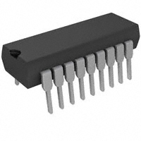


 工商网监
湘ICP备2023018690号
工商网监
湘ICP备2023018690号
