PIC16F87/88
18/20/28-Pin Enhanced Flash MCUs with nanoWatt Technology
Low-Power Features:
Pin Diagram
• Power-Managed modes:
- Primary Run: RC oscillator, 76 A, 1 MHz, 2V
- RC_RUN: 7 A, 31.25 kHz, 2V
- SEC_RUN: 9 A, 32 kHz, 2V
- Sleep: 0.1 A, 2V
• Timer1 Oscillator: 1.8 A, 32 kHz, 2V
• Watchdog Timer: 2.2 A, 2V
• Two-Speed Oscillator Start-up
18-Pin PDIP, SOIC
RA2/AN2/CVREF/
VREFRA3/AN3/VREF+/
C1OUT
RA4/AN4/T0CKI/
C2OUT
Flash # Single-Word
(bytes) Instructions
17
RA0/AN0
3
16
RA7/OSC1/CLKI
15
RA6/OSC2/CLKO
14
VDD
VSS
5
(1)
6
RB1/SDI/SDA
7
12
RB2/SDO/RX/DT
8
11
RB5/SS/TX/CK
(1)
9
10
RB4/SCK/SCL
Note 1:
13
RB7/AN6/PGD/
T1OSI
RB6/AN5/PGC/
T1OSO/T1CKI
The CCP1 pin is determined by the CCPMX bit in
Configuration Word 1 register.
Special Microcontroller Features:
• 100,000 erase/write cycles Enhanced Flash
program memory typical
• 1,000,000 typical erase/write cycles EEPROM
data memory typical
• EEPROM Data Retention: > 40 years
• In-Circuit Serial Programming™ (ICSP™)
via two pins
• Processor read/write access to program memory
• Low-Voltage Programming
• In-Circuit Debugging via two pins
• Extended Watchdog Timer (WDT):
- Programmable period from 1 ms to 268s
• Wide operating voltage range: 2.0V to 5.5V
• Capture, Compare, PWM (CCP) module:
- Capture is 16-bit, max. resolution is 12.5 ns
- Compare is 16-bit, max. resolution is 200 ns
- PWM max. resolution is 10-bit
• 10-bit, 7-channel Analog-to-Digital Converter
• Synchronous Serial Port (SSP) with SPI
(Master/Slave) and I2C™ (Slave)
• Addressable Universal Synchronous
Asynchronous Receiver Transmitter
(AUSART/SCI) with 9-bit address detection:
- RS-232 operation using internal oscillator
(no external crystal required)
• Dual Analog Comparator module:
- Programmable on-chip voltage reference
- Programmable input multiplexing from device
inputs and internal voltage reference
- Comparator outputs are externally accessible
Device
2
4
RB3/PGM/CCP1
Peripheral Features:
Program Memory
RA1/AN1
RA5/MCLR/VPP
RB0/INT/CCP1
• Three Crystal modes:
- LP, XT, HS: up to 20 MHz
• Two External RC modes
• One External Clock mode:
- ECIO: up to 20 MHz
• Internal oscillator block:
- 8 user selectable frequencies: 31 kHz,
125 kHz, 250 kHz, 500 kHz, 1 MHz, 2 MHz,
4 MHz, 8 MHz
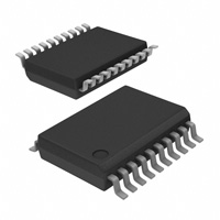
18
PIC16F88
Oscillators:
1
Data Memory
SRAM
(bytes)
EEPROM
(bytes)
I/O
Pins
10-bit
CCP
AUSART Comparators
A/D (ch) (PWM)
SSP
Timers
8/16-bit
PIC16F87
7168
4096
368
256
16
N/A
1
Y
2
Y
2/1
PIC16F88
7168
4096
368
256
16
1
1
Y
2
Y
2/1
2002-2013 Microchip Technology Inc.
DS30487D-page 1
�PIC16F87/88
Pin Diagrams
18-Pin PDIP, SOIC
1
18
RA1/AN1
2
17
RA0/AN0
RA4/T0CKI/C2OUT
RA5/MCLR/VPP
3
16
RA7/OSC1/CLKI
15
RA6/OSC2/CLKO
VSS
5
14
VDD
RB0/INT/CCP1(1)
6
13
RB7/PGD/T1OSI
RB1/SDI/SDA
7
12
RB6/PGC/T1OSO/T1CKI
RB2/SDO/RX/DT
8
11
RB5/SS/TX/CK
RB3/PGM/CCP1(1)
9
10
RB4/SCK/SCL
1
2
3
4
5
6
7
8
9
10
20
19
18
17
16
15
14
13
12
11
RA1/AN1
RA0/AN0
RA7/OSC1/CLKI
RA6/OSC2/CLKO
VDD
VDD
RB7/PGD/T1OSI
RB6/PGC/T1OSO/T1CKI
RB5/SS/TX/CK
RB4/SCK/SCL
4
PIC16F87
RA2/AN2/CVREF
RA3/AN3/C1OUT
RA2/AN2/CVREF
RA3/AN3/C1OUT
RA4/T0CKI/C2OUT
RA5/MCLR/VPP
VSS
VSS
RB0/INT/CCP1(1)
RB1/SDI/SDA
RB2/SDO/RX/DT
RB3/PGM/CCP1(1)
PIC16F87
20-Pin SSOP
18-Pin PDIP, SOIC
1
18
RA1/AN1
2
17
RA0/AN0
RA4/AN4/T0CKI/C2OUT
RA5/MCLR/VPP
3
16
RA7/OSC1/CLKI
15
RA6/OSC2/CLKO
VSS
5
14
VDD
RB0/INT/CCP1(1)
6
13
RB7/AN6/PGD/T1OSI
RB1/SDI/SDA
7
12
RB6/AN5/PGC/T1OSO/T1CKI
RB2/SDO/RX/DT
8
11
RB5/SS/TX/CK
RB3/PGM/CCP1(1)
9
10
RB4/SCK/SCL
1
2
3
4
5
6
7
8
9
10
20
19
18
17
16
15
14
13
12
11
RA1/AN1
RA0/AN0
RA7/OSC1/CLKI
RA6/OSC2/CLKO
VDD
VDD
RB7/AN6/PGD/T1OSI
RB6/AN5/PGC/T1OSO/T1CKI
RB5/SS/TX/CK
RB4/SCK/SCL
4
PIC16F88
RA2/AN2/CVREF/VREFRA3/AN3/VREF+/C1OUT
RA2/AN2/CVREF/VREFRA3/AN3/VREF+/C1OUT
RA4/AN4/T0CKI/C2OUT
RA5/MCLR1/VPP
VSS
VSS
RB0/INT/CCP1(1)
RB1/SDI/SDA
RB2/SDO/RX/DT
RB3/PGM/CCP1(1)
Note 1:
DS30487D-page 2
PIC16F88
20-Pin SSOP
The CCP1 pin is determined by the CCPMX bit in Configuration Word 1 register.
2002-2013 Microchip Technology Inc.
�PIC16F87/88
RA1/AN1
RA0/AN0
NC
23
22
25
24
RA2/AN2/CVREF
NC
26
RA4/T0CKI/C2OUT
RA3/AN3/C1OUT
27
28-Pin QFN(1)
28
Pin Diagrams (Cont’d)
RA5/MCLR/VPP
1
21
RA7/OSC1/CLKI
NC
VSS
2
20
RA6/OSC2/CLKO
3
19
VDD
NC
4
18
NC
VSS
5
17
VDD
NC
6
16
RB7/PGD/T1OSI
RB0/INT/CCP1(2)
7
15
RB6/PGC/T1OSO/T1CKI
14
NC
22
NC
13
12
RB4/SCK/SCL
RB5/SS/TX/CK
RA1/AN1
RA0/AN0
23
11
NC
24
10
RB3/PGM/CCP1(2)
RA2/AN2/CVREF/VREF-
NC
25
9
26
8
RB1/SDI/SDA
27
RB2/SDO/RX/DT
RA4/AN4/T0CKI/C2OUT
RA3/AN3/VREF+/C1OUT
28
28-Pin QFN(1)
PIC16F87
RA5/MCLR/VPP
1
21
RA7/OSC1/CLKI
NC
VSS
2
20
RA6/OSC2/CLKO
3
19
VDD
NC
4
18
NC
VSS
5
17
VDD
NC
6
16
RB7/AN6/PGD/T1OSI
RB0/INT/CCP1(2)
7
15
RB6/AN5/PGC/T1OSO/T1CKI
Note 1:
2:
8
9
10
11
12
13
14
RB1/SDI/SDA
RB2/SDO/RX/DT
RB3/PGM/CCP1(2)
NC
RB4/SCK/SCL
RB5/SS/TX/CK
NC
PIC16F88
For the QFN package, it is recommended that the bottom pad be connected to VSS.
The CCP1 pin is determined by the CCPMX bit in Configuration Word 1 register.
2002-2013 Microchip Technology Inc.
DS30487D-page 3
�PIC16F87/88
Table of Contents
1.0 Device Overview .......................................................................................................................................................................... 5
2.0 Memory Organization ................................................................................................................................................................. 11
3.0 Data EEPROM and Flash Program Memory.............................................................................................................................. 27
4.0 Oscillator Configurations ............................................................................................................................................................ 35
5.0 I/O Ports ..................................................................................................................................................................................... 51
6.0 Timer0 Module ........................................................................................................................................................................... 67
7.0 Timer1 Module ........................................................................................................................................................................... 71
8.0 Timer2 Module ........................................................................................................................................................................... 79
9.0 Capture/Compare/PWM (CCP) Module ..................................................................................................................................... 81
10.0 Synchronous Serial Port (SSP) Module ..................................................................................................................................... 87
11.0 Addressable Universal Synchronous Asynchronous Receiver Transmitter (AUSART) ............................................................. 97
12.0 Analog-to-Digital Converter (A/D) Module ................................................................................................................................ 113
13.0 Comparator Module.................................................................................................................................................................. 121
14.0 Comparator Voltage Reference Module ................................................................................................................................... 127
15.0 Special Features of the CPU .................................................................................................................................................... 129
16.0 Instruction Set Summary .......................................................................................................................................................... 149
17.0 Development Support............................................................................................................................................................... 157
18.0 Electrical Characteristics .......................................................................................................................................................... 161
19.0 DC and AC Characteristics Graphs and Tables ....................................................................................................................... 191
20.0 Packaging Information.............................................................................................................................................................. 205
Appendix A: Revision History............................................................................................................................................................. 215
Appendix B: Device Differences......................................................................................................................................................... 215
INDEX ................................................................................................................................................................................................ 217
The Microchip Web Site ..................................................................................................................................................................... 225
Customer Change Notification Service .............................................................................................................................................. 225
Customer Support .............................................................................................................................................................................. 225
Reader Response .............................................................................................................................................................................. 226
PIC16F87/88 Product Identification System ...................................................................................................................................... 227
TO OUR VALUED CUSTOMERS
It is our intention to provide our valued customers with the best documentation possible to ensure successful use of your Microchip
products. To this end, we will continue to improve our publications to better suit your needs. Our publications will be refined and
enhanced as new volumes and updates are introduced.
If you have any questions or comments regarding this publication, please contact the Marketing Communications Department via
E-mail at docerrors@microchip.com or fax the Reader Response Form in the back of this data sheet to (480) 792-4150. We
welcome your feedback.
Most Current Data Sheet
To obtain the most up-to-date version of this data sheet, please register at our Worldwide Web site at:
http://www.microchip.com
You can determine the version of a data sheet by examining its literature number found on the bottom outside corner of any page.
The last character of the literature number is the version number, (e.g., DS30000A is version A of document DS30000).
Errata
An errata sheet, describing minor operational differences from the data sheet and recommended workarounds, may exist for current
devices. As device/documentation issues become known to us, we will publish an errata sheet. The errata will specify the revision
of silicon and revision of document to which it applies.
To determine if an errata sheet exists for a particular device, please check with one of the following:
• Microchip’s Worldwide Web site; http://www.microchip.com
• Your local Microchip sales office (see last page)
When contacting a sales office, please specify which device, revision of silicon and data sheet (include literature number) you are
using.
Customer Notification System
Register on our web site at www.microchip.com to receive the most current information on all of our products.
DS30487D-page 4
2002-2013 Microchip Technology Inc.
�PIC16F87/88
1.0
DEVICE OVERVIEW
This document contains device specific information for
the operation of the PIC16F87/88 devices. Additional
information may be found in the “PIC® Mid-Range MCU
Family Reference Manual” (DS33023) which may be
downloaded from the Microchip web site. This
Reference Manual should be considered a complementary document to this data sheet and is highly
recommended reading for a better understanding of the
device architecture and operation of the peripheral
modules.
The PIC16F87/88 belongs to the Mid-Range family of
the PIC® devices. Block diagrams of the devices are
shown in Figure 1-1 and Figure 1-2. These devices
contain features that are new to the PIC16 product line:
• Low-power modes: RC_RUN allows the core and
peripherals to be clocked from the INTRC, while
SEC_RUN allows the core and peripherals to be
clocked from the low-power Timer1. Refer to
Section 4.7 “Power-Managed Modes” for
further details.
• Internal RC oscillator with eight selectable
frequencies, including 31.25 kHz, 125 kHz,
250 kHz, 500 kHz, 1 MHz, 2 MHz, 4 MHz and
8 MHz. The INTRC can be configured as a
primary or secondary clock source. Refer to
Section 4.5 “Internal Oscillator Block” for
further details.
• The Timer1 module current consumption has
been greatly reduced from 20 A (previous PIC16
devices) to 1.8 A typical (32 kHz at 2V), which is
ideal for real-time clock applications. Refer to
Section 7.0 “Timer1 Module” for further details.
• Extended Watchdog Timer (WDT) that can have a
programmable period from 1 ms to 268s. The
WDT has its own 16-bit prescaler. Refer to
Section 15.12 “Watchdog Timer (WDT)” for
further details.
• Two-Speed Start-up: When the oscillator is
configured for LP, XT or HS Oscillator mode, this
feature will clock the device from the INTRC while
the oscillator is warming up. This, in turn, will
enable almost immediate code execution. Refer
to Section 15.12.3 “Two-Speed Clock Start-up
Mode” for further details.
• Fail-Safe Clock Monitor: This feature will allow the
device to continue operation if the primary or
secondary clock source fails by switching over to
the INTRC.
• The A/D module has a new register for PIC16
devices named ANSEL. This register allows
easier configuration of analog or digital I/O pins.
2002-2013 Microchip Technology Inc.
TABLE 1-1:
AVAILABLE MEMORY IN
PIC16F87/88 DEVICES
Device
Program
Flash
Data
Memory
Data
EEPROM
PIC16F87/88
4K x 14
368 x 8
256 x 8
There are 16 I/O pins that are user configurable on a
pin-to-pin basis. Some pins are multiplexed with other
device functions. These functions include:
•
•
•
•
•
•
•
•
•
•
External Interrupt
Change on PORTB Interrupt
Timer0 Clock Input
Low-Power Timer1 Clock/Oscillator
Capture/Compare/PWM
10-bit, 7-channel A/D Converter (PIC16F88 only)
SPI/I2C™
Two Analog Comparators
AUSART
MCLR (RA5) can be configured as an input
Table 1-2 details the pinout of the devices with
descriptions and details for each pin.
DS30487D-page 5
�PIC16F87/88
FIGURE 1-1:
PIC16F87 DEVICE BLOCK DIAGRAM
13
Program
Memory
Program
Bus
14
RAM Addr(1)
RA0/AN0
RA1/AN1
RA2/AN2/CVREF
RA3/AN3/C1OUT
RA4/T0CKI/C2OUT
RA5/MCLR/VPP
RA6/OSC2/CLKO
RA7/OSC1/CLKI
9
PORTB
Addr MUX
Instruction reg
7
Direct Addr
PORTA
RAM
File
Registers
368 x 8
8 Level Stack
(13-bit)
4K x 14
8
Data Bus
Program Counter
Flash
8
RB0/INT/CCP1(2)
RB1/SDI/SDA
RB2/SDO/RX/DT
RB3/PGM/CCP1(2)
RB4/SCK/SCL
RB5/SS/TX/CK
RB6/PGC/T1OSO/T1CKI
RB7/PGD/T1OSI
Indirect
Addr
FSR reg
STATUS reg
8
3
Power-up
Timer
Instruction
Decode &
Control
Timing
Generation
OSC1/CLKI
OSC2/CLKO
Oscillator
Start-up Timer
Note 1:
2:
ALU
Power-on
Reset
8
Watchdog
Timer
Brown-out
Reset
RA5/MCLR
MUX
W reg
VDD, VSS
Timer2
Timer1
Timer0
SSP
AUSART
CCP1
Data EE
256 Bytes
Comparators
Higher order bits are from the STATUS register.
The CCP1 pin is determined by the CCPMX bit in Configuration Word 1 register.
DS30487D-page 6
2002-2013 Microchip Technology Inc.
�PIC16F87/88
FIGURE 1-2:
PIC16F88 DEVICE BLOCK DIAGRAM
13
Program
Memory
Program
Bus
14
RAM Addr(1)
RA0/AN0
RA1/AN1
RA2/AN2/CVREF/VREFRA3/AN3/VREF+/C1OUT
RA4/AN4/T0CKI/C2OUT
RA5/MCLR/VPP
RA6/OSC2/CLKO
RA7/OSC1/CLKI
9
PORTB
Addr MUX
Instruction reg
7
Direct Addr
PORTA
RAM
File
Registers
368 x 8
8 Level Stack
(13-bit)
4K x 14
8
Data Bus
Program Counter
Flash
8
RB0/INT/CCP1(2)
RB1/SDI/SDA
RB2/SDO/RX/DT
RB3/PGM/CCP1(2)
RB4/SCK/SCL
RB5/SS/TX/CK
RB6/AN5/PGC/T1OSO/T1CKI
RB7/AN6/PGD/T1OSI
Indirect
Addr
FSR reg
STATUS reg
8
3
Power-up
Timer
Instruction
Decode &
Control
Timing
Generation
OSC1/CLKI
OSC2/CLKO
Oscillator
Start-up Timer
Note 1:
2:
ALU
Power-on
Reset
8
Watchdog
Timer
Brown-out
Reset
RA5/MCLR
MUX
W reg
VDD, VSS
Timer2
Timer1
Timer0
10-bit A/D
AUSART
CCP1
Data EE
256 Bytes
Comparators
SSP
Higher order bits are from the STATUS register.
The CCP1 pin is determined by the CCPMX bit in Configuration Word 1 register.
2002-2013 Microchip Technology Inc.
DS30487D-page 7
�PIC16F87/88
TABLE 1-2:
PIC16F87/88 PINOUT DESCRIPTION
PDIP/
SOIC
Pin#
SSOP
Pin#
QFN
Pin#
RA0/AN0
RA0
AN0
17
19
23
RA1/AN1
RA1
AN1
18
RA2/AN2/CVREF/VREFRA2
AN2
CVREF
VREF-(4)
1
RA3/AN3/VREF+/C1OUT
RA3
AN3
VREF+(4)
C1OUT
2
RA4/AN4/T0CKI/C2OUT
RA4
AN4(4)
T0CKI
C2OUT
3
RA5/MCLR/VPP
RA5
MCLR
4
Pin Name
I/O/P
Type
Buffer
Type
Description
PORTA is a bidirectional I/O port.
20
1
2
3
4
15
17
Legend:
Note 1:
2:
3:
4:
5:
16
18
Bidirectional I/O pin.
Analog input channel 0.
I/O
I
TTL
Analog
Bidirectional I/O pin.
Analog input channel 1.
I/O
I
O
I
TTL
Analog
Bidirectional I/O pin.
Analog input channel 2.
Comparator VREF output.
A/D reference voltage (Low) input.
I/O
I
I
O
TTL
Analog
Analog
Bidirectional I/O pin.
Analog input channel 3.
A/D reference voltage (High) input.
Comparator 1 output.
I/O
I
I
O
ST
Analog
ST
Bidirectional I/O pin.
Analog input channel 4.
Clock input to the TMR0 timer/counter.
Comparator 2 output.
I
I
ST
ST
P
–
I/O
O
ST
–
O
–
I/O
I
I
ST
ST/CMOS(3)
–
26
Analog
27
28
1
Input pin.
Master Clear (Reset). Input/programming voltage
input. This pin is an active-low Reset to the device.
Programming voltage input.
20
CLKO
RA7/OSC1/CLKI
RA7
OSC1
CLKI
TTL
Analog
24
VPP
RA6/OSC2/CLKO
RA6
OSC2
I/O
I
Bidirectional I/O pin.
Oscillator crystal output. Connects to crystal or
resonator in Crystal Oscillator mode.
In RC mode, this pin outputs CLKO signal which has
1/4 the frequency of OSC1 and denotes the
instruction cycle rate.
21
Bidirectional I/O pin.
Oscillator crystal input.
External clock source input.
I = Input
O
= Output
I/O = Input/Output
P = Power
– = Not used
TTL = TTL Input
ST = Schmitt Trigger Input
This buffer is a Schmitt Trigger input when configured as the external interrupt.
This buffer is a Schmitt Trigger input when used in Serial Programming mode.
This buffer is a Schmitt Trigger input when configured in RC Oscillator mode and a CMOS input otherwise.
PIC16F88 devices only.
The CCP1 pin is determined by the CCPMX bit in Configuration Word 1 register.
DS30487D-page 8
2002-2013 Microchip Technology Inc.
�PIC16F87/88
TABLE 1-2:
PIC16F87/88 PINOUT DESCRIPTION (CONTINUED)
Pin Name
PDIP/
SOIC
Pin#
SSOP
Pin#
QFN
Pin#
I/O/P
Type
Buffer
Type
Description
PORTB is a bidirectional I/O port. PORTB can be
software programmed for internal weak pull-up on all
inputs.
RB0/INT/CCP1(5)
RB0
INT
CCP1
6
RB1/SDI/SDA
RB1
SDI
SDA
7
RB2/SDO/RX/DT
RB2
SDO
RX
DT
8
RB3/PGM/CCP1(5)
RB3
PGM
CCP1
9
RB4/SCK/SCL
RB4
SCK
SCL
10
RB5/SS/TX/CK
RB5
SS
TX
CK
11
RB6/AN5/PGC/T1OSO/
T1CKI
RB6
AN5(4)
PGC
T1OSO
T1CKI
12
RB7/AN6/PGD/T1OSI
RB7
AN6(4)
PGD
T1OSI
13
VSS
5
14
Note 1:
2:
3:
4:
5:
8
9
10
11
12
13
14
7
I/O
I
I/O
TTL
ST(1)
ST
Bidirectional I/O pin.
External interrupt pin.
Capture input, Compare output, PWM output.
I/O
I
I/O
TTL
ST
ST
Bidirectional I/O pin.
SPI data in.
I2C™ data.
I/O
O
I
I/O
TTL
ST
Bidirectional I/O pin.
SPI data out.
AUSART asynchronous receive.
AUSART synchronous detect.
I/O
I/O
I
TTL
ST
ST
Bidirectional I/O pin.
Low-Voltage ICSP™ Programming enable pin.
Capture input, Compare output, PWM output.
I/O
I/O
I
TTL
ST
ST
Bidirectional I/O pin. Interrupt-on-change pin.
Synchronous serial clock input/output for SPI.
Synchronous serial clock Input for I2C.
I/O
I
O
I/O
TTL
TTL
Bidirectional I/O pin. Interrupt-on-change pin.
Slave select for SPI in Slave mode.
AUSART asynchronous transmit.
AUSART synchronous clock.
I/O
I
I/O
O
I
TTL
Bidirectional I/O pin. Interrupt-on-change pin.
Analog input channel 5.
In-Circuit Debugger and programming clock pin.
Timer1 oscillator output.
Timer1 external clock input.
8
9
10
12
13
15
5, 6
ST(2)
ST
ST
16
I/O
I
I
I
VDD
Legend:
7
3, 5
15, 16 17, 19
TTL
ST(2)
ST
Bidirectional I/O pin. Interrupt-on-change pin.
Analog input channel 6.
In-Circuit Debugger and ICSP programming data pin.
Timer1 oscillator input.
P
–
Ground reference for logic and I/O pins.
P
–
Positive supply for logic and I/O pins.
I = Input
O
= Output
I/O = Input/Output
P = Power
– = Not used
TTL = TTL Input
ST = Schmitt Trigger Input
This buffer is a Schmitt Trigger input when configured as the external interrupt.
This buffer is a Schmitt Trigger input when used in Serial Programming mode.
This buffer is a Schmitt Trigger input when configured in RC Oscillator mode and a CMOS input otherwise.
PIC16F88 devices only.
The CCP1 pin is determined by the CCPMX bit in Configuration Word 1 register.
2002-2013 Microchip Technology Inc.
DS30487D-page 9
�PIC16F87/88
NOTES:
DS30487D-page 10
2002-2013 Microchip Technology Inc.
�PIC16F87/88
2.0
MEMORY ORGANIZATION
FIGURE 2-1:
There are two memory blocks in the PIC16F87/88
devices. These are the program memory and the data
memory. Each block has its own bus, so access to each
block can occur during the same oscillator cycle.
PC
CALL, RETURN
RETFIE, RETLW
The data memory can be further broken down into the
general purpose RAM and the Special Function
Registers (SFRs). The operation of the SFRs that
control the “core” are described here. The SFRs used
to control the peripheral modules are described in the
section discussing each individual peripheral module.
The data memory area also contains the data EEPROM
memory. This memory is not directly mapped into the
data memory but is indirectly mapped. That is, an indirect address pointer specifies the address of the data
EEPROM memory to read/write. The PIC16F87/88
device’s 256 bytes of data EEPROM memory have the
address range of 00h-FFh. More details on the
EEPROM memory can be found in Section 3.0 “Data
EEPROM and Flash Program Memory”.
Additional information on device memory may be found
in the “PIC® Mid-Range MCU Family Reference Manual” (DS33023).
2.1
PROGRAM MEMORY MAP
AND STACK: PIC16F87/88
13
Stack Level 1
Stack Level 2
Stack Level 8
Reset Vector
0000h
Interrupt Vector
0004h
0005h
Page 0
On-Chip
Program
Memory
07FFh
0800h
Page 1
0FFFh
1000h
Program Memory Organization
The PIC16F87/88 devices have a 13-bit program counter capable of addressing an 8K x 14 program memory
space. For the PIC16F87/88, the first 4K x 14 (0000h0FFFh) is physically implemented (see Figure 2-1).
Accessing a location above the physically implemented
address will cause a wraparound. For example, the
same instruction will be accessed at locations 020h,
420h, 820h, C20h, 1020h, 1420h, 1820h and 1C20h.
The Reset vector is at 0000h and the interrupt vector is
at 0004h.
Wraps to
0000h-03FFh
1FFFh
2.2
Data Memory Organization
The data memory is partitioned into multiple banks that
contain the General Purpose Registers and the Special
Function Registers. Bits RP1 (STATUS) and RP0
(STATUS) are the bank select bits.
RP1:RP0
Bank
00
0
01
1
10
2
11
3
Each bank extends up to 7Fh (128 bytes). The lower
locations of each bank are reserved for the Special
Function Registers. Above the Special Function Registers are General Purpose Registers, implemented as
static RAM. All implemented banks contain SFRs.
Some “high use” SFRs from one bank may be mirrored
in another bank for code reduction and quicker access
(e.g., the STATUS register is in Banks 0-3).
Note:
2002-2013 Microchip Technology Inc.
EEPROM data memory description can be
found in Section 3.0 “Data EEPROM and
Flash Program Memory” of this data
sheet.
DS30487D-page 11
�PIC16F87/88
2.2.1
GENERAL PURPOSE REGISTER FILE
The register file can be accessed either directly, or
indirectly, through the File Select Register (FSR).
FIGURE 2-2:
PIC16F87 REGISTER FILE MAP
Indirect addr.(*)
TMR0
PCL
STATUS
FSR
PORTA
PORTB
PCLATH
INTCON
PIR1
PIR2
TMR1L
TMR1H
T1CON
TMR2
T2CON
SSPBUF
SSPCON
CCPR1L
CCPR1H
CCP1CON
RCSTA
TXREG
RCREG
00h
01h
02h
03h
04h
05h
06h
07h
08h
09h
0Ah
0Bh
0Ch
0Dh
0Eh
0Fh
10h
11h
12h
13h
14h
15h
16h
17h
18h
19h
1Ah
1Bh
1Ch
1Dh
Indirect addr.(*)
OPTION_REG
PCL
STATUS
FSR
TRISA
TRISB
PCLATH
INTCON
PIE1
PIE2
PCON
OSCCON
OSCTUNE
PR2
SSPADD
SSPSTAT
TXSTA
SPBRG
CMCON
CVRCON
1Eh
1Fh
20h
General
Purpose
Register
80 Bytes
General
Purpose
Register
96 Bytes
accesses
70h-7Fh
7Fh
Bank 0
*
Note 1:
80h
81h
82h
83h
84h
85h
86h
87h
88h
89h
8Ah
8Bh
8Ch
8Dh
8Eh
8Fh
90h
91h
92h
93h
94h
95h
96h
97h
98h
99h
9Ah
9Bh
9Ch
9Dh
9Eh
9Fh
A0h
EFh
F0h
FFh
Bank 1
File
Address
File
Address
File
Address
File
Address
Indirect addr.(*)
TMR0
PCL
STATUS
FSR
WDTCON
PORTB
PCLATH
INTCON
EEDATA
EEADR
EEDATH
EEADRH
100h
101h
102h
103h
104h
105h
106h
107h
108h
109h
10Ah
10Bh
10Ch
10Dh
10Eh
10Fh
110h
Indirect addr.(*)
OPTION_REG
PCL
STATUS
FSR
TRISB
PCLATH
INTCON
EECON1
EECON2
Reserved(1)
Reserved(1)
General
Purpose
Register
16 Bytes
General
Purpose
Register
16 Bytes
19Fh
1A0h
11Fh
120h
General
Purpose
Register
80 Bytes
General
Purpose
Register
80 Bytes
accesses
70h-7Fh
16Fh
170h
accesses
70h-7Fh
17Fh
Bank 2
180h
181h
182h
183h
184h
185h
186h
187h
188h
189h
18Ah
18Bh
18Ch
18Dh
18Eh
18Fh
190h
1EFh
1F0h
1FFh
Bank 3
Unimplemented data memory locations, read as ‘0’.
Not a physical register.
This register is reserved, maintain this register clear.
DS30487D-page 12
2002-2013 Microchip Technology Inc.
�PIC16F87/88
FIGURE 2-3:
PIC16F88 REGISTER FILE MAP
File
Address
File
Address
Indirect addr.(*)
TMR0
PCL
STATUS
FSR
PORTA
PORTB
PCLATH
INTCON
PIR1
PIR2
TMR1L
TMR1H
T1CON
TMR2
T2CON
SSPBUF
SSPCON
CCPR1L
CCPR1H
CCP1CON
RCSTA
TXREG
RCREG
ADRESH
ADCON0
00h
01h
02h
03h
04h
05h
06h
07h
08h
09h
0Ah
0Bh
0Ch
0Dh
0Eh
0Fh
10h
11h
12h
13h
14h
15h
16h
17h
18h
19h
1Ah
1Bh
1Ch
1Dh
1Eh
1Fh
20h
Indirect addr.(*)
80h
OPTION_REG 81h
PCL
82h
STATUS
83h
FSR
84h
TRISA
85h
TRISB
86h
87h
88h
89h
PCLATH
8Ah
INTCON
8Bh
PIE1
8Ch
PIE2
8Dh
PCON
8Eh
OSCCON
8Fh
OSCTUNE
90h
91h
PR2
92h
SSPADD
93h
SSPSTAT
94h
95h
96h
97h
TXSTA
98h
SPBRG
99h
9Ah
ANSEL
9Bh
CMCON
9Ch
CVRCON
9Dh
ADRESL
9Eh
9Fh
ADCON1
General
Purpose
Register
80 Bytes
General
Purpose
Register
A0h
7Fh
Bank 0
Note 1:
FFh
Bank 1
Indirect addr.(*)
OPTION_REG
PCL
STATUS
FSR
TRISB
PCLATH
INTCON
EECON1
EECON2
Reserved(1)
Reserved(1)
19Fh
1A0h
11Fh
120h
General
Purpose
Register
80 Bytes
General
Purpose
Register
80 Bytes
16Fh
170h
1EFh
1F0h
accesses
70h-7Fh
17Fh
Bank 2
180h
181h
182h
183h
184h
185h
186h
187h
188h
189h
18Ah
18Bh
18Ch
18Dh
18Eh
18Fh
190h
General
Purpose
Register
16 Bytes
General
Purpose
Register
16 Bytes
accesses
70h-7Fh
accesses
70h-7Fh
*
Indirect addr.(*) 100h
101h
TMR0
102h
PCL
103h
STATUS
104h
FSR
WDTCON
105h
106h
PORTB
107h
108h
109h
10Ah
PCLATH
10Bh
INTCON
10Ch
EEDATA
10Dh
EEADR
10Eh
EEDATH
10Fh
EEADRH
110h
EFh
F0h
96 Bytes
File
Address
File
Address
1FFh
Bank 3
Unimplemented data memory locations, read as ‘0’.
Not a physical register.
This register is reserved, maintain this register clear.
2002-2013 Microchip Technology Inc.
DS30487D-page 13
�PIC16F87/88
2.2.2
SPECIAL FUNCTION REGISTERS
The Special Function Registers are registers used by
the CPU and peripheral modules for controlling the
desired operation of the device. These registers are
implemented as static RAM. A list of these registers is
given in Table 2-1.
TABLE 2-1:
Address
The Special Function Registers can be classified into
two sets: core (CPU) and peripheral. Those registers
associated with the core functions are described in
detail in this section. Those related to the operation of
the peripheral features are described in detail in the
peripheral feature section.
SPECIAL FUNCTION REGISTER SUMMARY
Name
Bit 7
Bit 6
Bit 5
Bit 4
Bit 3
Bit 2
Bit 1
Bit 0
Value on:
POR, BOR
Details
on
page
Bank 0
00h(2)
INDF
Addressing this location uses contents of FSR to address data memory (not a physical register)
0000 0000
26, 135
01h
TMR0
Timer0 Module Register
xxxx xxxx
69
02h(2)
PCL
Program Counter (PC) Least Significant Byte
0000 0000
03h(2)
STATUS
0001 1xxx
17
04h(2)
FSR
Indirect Data Memory Address Pointer
xxxx xxxx
135
05h
PORTA
PORTA Data Latch when written; PORTA pins when read (PIC16F87)
PORTA Data Latch when written; PORTA pins when read (PIC16F88)
xxxx 0000
xxx0 0000
52
06h
PORTB
PORTB Data Latch when written; PORTB pins when read (PIC16F87)
PORTB Data Latch when written; PORTB pins when read (PIC16F88)
xxxx xxxx
00xx xxxx
58
IRP
RP1
RP0
TO
PD
Z
DC
C
07h
—
Unimplemented
—
—
08h
—
Unimplemented
—
—
09h
—
Unimplemented
—
—
---0 0000
135
0Ah(1,2)
PCLATH
—
—
—
0Bh(2)
INTCON
GIE
PEIE
TMR0IE
0Ch
PIR1
—
ADIF(4)
0Dh
PIR2
OSFIF
CMIF
0Eh
TMR1L
0Fh
TMR1H
10h
T1CON
11h
TMR2
12h
T2CON
13h
SSPBUF
14h
SSPCON
15h
CCPR1L
16h
CCPR1H
17h
CCP1CON
18h
RCSTA
19h
TXREG
1Ah
RCREG
1Bh
—
1Ch
1Dh
TMR0IF
INT0IF
RBIF
0000 000x
19, 69,
77
RCIF
TXIF
SSPIF
CCP1IF
TMR2IF
TMR1IF
-000 0000
21, 77
—
EEIF
—
—
—
—
00-0 ----
23, 34
Holding Register for the Least Significant Byte of the 16-bit TMR1 Register
xxxx xxxx
77, 83
Holding Register for the Most Significant Byte of the 16-bit TMR1 Register
xxxx xxxx
77, 83
72, 83
—
T1RUN
T1CKPS1
T1CKPS0
T1OSCEN
T1SYNC
TMR1CS
TMR1ON
-000 0000
0000 0000
80, 85
TOUTPS2
TOUTPS1
TOUTPS0
TMR2ON
T2CKPS1
T2CKPS0
-000 0000
80, 85
xxxx xxxx
90, 95
SSPM2
SSPM1
SSPM0
0000 0000
89, 95
Capture/Compare/PWM Register 1 (LSB)
xxxx xxxx
83, 85
Capture/Compare/PWM Register 1 (MSB)
xxxx xxxx
83, 85
—
TOUTPS3
Synchronous Serial Port Receive Buffer/Transmit Register
WCOL
SSPOV
SSPEN
CKP
SSPM3
—
CCP1X
CCP1Y
CCP1M3
CCP1M2
CCP1M1
CCP1M0
--00 0000
81, 83
SPEN
RX9
SREN
CREN
ADDEN
FERR
OERR
RX9D
0000 000x
98, 99
AUSART Transmit Data Register
0000 0000
103
AUSART Receive Data Register
0000 0000
105
Unimplemented
—
—
—
Unimplemented
—
—
—
Unimplemented
—
—
xxxx xxxx
120
1Fh
ADCON0(4)
2:
3:
4:
RBIE
—
ADRESH(4)
Note 1:
INT0IE
Timer2 Module Register
1Eh
Legend:
Write Buffer for the Upper 5 bits of the Program Counter
A/D Result Register High Byte
ADCS1
ADCS0
CHS2
CHS1
CHS0
GO/DONE
—
ADON
0000 00-0 114, 120
x = unknown, u = unchanged, q = value depends on condition, - = unimplemented, read as ‘0’, r = reserved.
Shaded locations are unimplemented, read as ‘0’.
The upper byte of the program counter is not directly accessible. PCLATH is a holding register for PC, whose
contents are transferred to the upper byte of the program counter.
These registers can be addressed from any bank.
RA5 is an input only; the state of the TRISA5 bit has no effect and will always read ‘1’.
PIC16F88 device only.
DS30487D-page 14
2002-2013 Microchip Technology Inc.
�PIC16F87/88
TABLE 2-1:
Address
SPECIAL FUNCTION REGISTER SUMMARY (CONTINUED)
Name
Bit 7
Bit 6
Bit 5
Bit 4
Bit 3
Bit 2
Bit 1
Bit 0
Value on:
POR, BOR
Details
on
page
0000 0000
26, 135
1111 1111
18, 69
0000 0000
135
Bank 1
80h(2)
INDF
81h
OPTION_REG
82h(2)
PCL
83h(2)
STATUS
(2)
Addressing this location uses contents of FSR to address data memory (not a physical register)
RBPU
INTEDG
T0CS
T0SE
PSA
PS2
PS1
PS0
Program Counter (PC) Least Significant Byte
84h
FSR
85h
TRISA
86h
TRISB
IRP
RP1
RP0
TO
PD
Z
DC
C
Indirect Data Memory Address Pointer
TRISA7
TRISA6
TRISA5(3) PORTA Data Direction Register (TRISA)
PORTB Data Direction Register
0001 1xxx
17
xxxx xxxx
135
1111 1111
52, 126
1111 1111
58, 85
87h
—
Unimplemented
—
—
88h
—
Unimplemented
—
—
—
Unimplemented
89h
8Ah(1,2)
PCLATH
—
—
—
8Bh(2)
INTCON
GIE
PEIE
TMR0IE
8Ch
PIE1
—
ADIE(4)
8Dh
PIE2
OSFIE
CMIE
8Eh
PCON
—
8Fh
OSCCON
90h
OSCTUNE
91h
—
Write Buffer for the Upper 5 bits of the Program Counter
—
—
---0 0000
135
INT0IE
RBIE
TMR0IF
INT0IF
RBIF
0000 000x
19, 69,
77
RCIE
TXIE
SSPIE
CCP1IE
TMR2IE
TMR1IE
-000 0000
20, 80
—
EEIE
—
—
—
—
00-0 ----
22, 34
—
—
—
—
—
POR
BOR
---- --0q
24
—
IRCF2
IRCF1
IRCF0
OSTS
IOFS
SCS1
SCS0
-000 0000
40
—
—
TUN5
TUN4
TUN3
TUN2
TUN1
TUN0
--00 0000
38
—
—
80, 85
Unimplemented
92h
PR2
Timer2 Period Register
1111 1111
93h
SSPADD
Synchronous Serial Port (I2C™ mode) Address Register
0000 0000
95
94h
SSPSTAT
0000 0000
88, 95
SMP
CKE
D/A
P
S
R/W
UA
BF
95h
—
Unimplemented
—
—
96h
—
Unimplemented
—
—
97h
—
Unimplemented
—
—
0000 -010
97, 99
0000 0000
99, 103
98h
TXSTA
99h
SPBRG
9Ah
—
CSRC
TX9
TXEN
SYNC
—
BRGH
TRMT
TX9D
Baud Rate Generator Register
Unimplemented
—
—
9Bh
ANSEL(4)
—
ANS6
ANS5
ANS4
ANS3
ANS2
ANS1
ANS0
-111 1111
120
9Ch
CMCON
C2OUT
C1OUT
C2INV
C1INV
CIS
CM2
CM1
CM0
0000 0111
121,
126, 128
9Dh
CVRCON
CVREN
CVROE
CVRR
—
CVR3
CVR2
CVR1
CVR0
000- 0000 126, 128
(4)
9Eh
ADRESL
9Fh
ADCON1(4)
Legend:
Note 1:
2:
3:
4:
A/D Result Register Low Byte
ADFM
ADCS2
VCFG1
VCFG0
—
—
—
—
xxxx xxxx
120
0000 ----
52, 115,
120
x = unknown, u = unchanged, q = value depends on condition, - = unimplemented, read as ‘0’, r = reserved.
Shaded locations are unimplemented, read as ‘0’.
The upper byte of the program counter is not directly accessible. PCLATH is a holding register for PC, whose
contents are transferred to the upper byte of the program counter.
These registers can be addressed from any bank.
RA5 is an input only; the state of the TRISA5 bit has no effect and will always read ‘1’.
PIC16F88 device only.
2002-2013 Microchip Technology Inc.
DS30487D-page 15
�PIC16F87/88
TABLE 2-1:
Address
SPECIAL FUNCTION REGISTER SUMMARY (CONTINUED)
Name
Value on:
POR, BOR
Details
on
page
Addressing this location uses contents of FSR to address data memory (not a physical register)
0000 0000
26, 135
Bit 7
Bit 6
Bit 5
Bit 4
Bit 3
Bit 2
Bit 1
Bit 0
Bank 2
100h(2)
INDF
101h
TMR0
Timer0 Module Register
xxxx xxxx
69
102h(2)
PCL
Program Counter’s (PC) Least Significant Byte
0000 0000
135
103h(2)
STATUS
104h(2)
FSR
105h
WDTCON
106h
PORTB
IRP
RP1
RP0
TO
PD
Z
DC
C
Indirect Data Memory Address Pointer
—
—
—
WDTPS3
WDTPS2
WDTPS1
WDTPS0
SWDTEN
PORTB Data Latch when written; PORTB pins when read (PIC16F87)
PORTB Data Latch when written; PORTB pins when read (PIC16F88)
0001 1xxx
17
xxxx xxxx
135
---0 1000
142
xxxx xxxx
00xx xxxx
58
107h
—
Unimplemented
—
—
108h
—
Unimplemented
—
—
109h
—
Unimplemented
—
—
---0 0000
135
0000 000x
19, 69,
77
10Ah(1,2) PCLATH
—
—
—
GIE
PEIE
TMR0IE
Write Buffer for the Upper 5 bits of the Program Counter
10Bh(2)
INTCON
10Ch
EEDATA
EEPROM/Flash Data Register Low Byte
xxxx xxxx
34
10Dh
EEADR
EEPROM/Flash Address Register Low Byte
xxxx xxxx
34
10Eh
EEDATH
—
—
10Fh
EEADRH
—
—
INT0IE
RBIE
TMR0IF
INT0IF
RBIF
EEPROM/Flash Data Register High Byte
—
—
EEPROM/Flash Address Register High Byte
--xx xxxx
34
---- xxxx
34
Bank 3
180h(2)
INDF
181h
OPTION_REG
182h(2)
PCL
183h(2)
STATUS
(2)
184h
Addressing this location uses contents of FSR to address data memory (not a physical register)
T0CS
T0SE
PSA
PS2
PS1
PS0
IRP
RP1
RP0
TO
PD
Z
DC
C
Indirect Data Memory Address Pointer
—
186h
INTEDG
Program Counter (PC) Least Significant Byte
FSR
185h
RBPU
TRISB
Unimplemented
PORTB Data Direction Register
0000 0000
135
1111 1111
18, 69
0000 0000
135
0001 1xxx
17
xxxx xxxx
135
—
—
1111 1111
58, 83
187h
—
Unimplemented
—
—
188h
—
Unimplemented
—
—
189h
—
Unimplemented
—
—
---0 0000
135
18Ah(1,2) PCLATH
18Bh(2)
INTCON
18Ch
EECON1
18Dh
EECON2
18Eh
18Fh
Legend:
Note 1:
2:
3:
4:
—
—
—
Write Buffer for the Upper 5 bits of the Program Counter
GIE
PEIE
TMR0IE
INT0IE
RBIE
TMR0IF
INT0IF
RBIF
0000 000x
19, 69,
77
EEPGD
—
—
FREE
WRERR
WREN
WR
RD
x--x x000
28, 34
EEPROM Control Register 2 (not a physical register)
---- ----
34
—
Reserved, maintain clear
0000 0000
—
—
Reserved, maintain clear
0000 0000
—
x = unknown, u = unchanged, q = value depends on condition, - = unimplemented, read as ‘0’, r = reserved.
Shaded locations are unimplemented, read as ‘0’.
The upper byte of the program counter is not directly accessible. PCLATH is a holding register for PC, whose
contents are transferred to the upper byte of the program counter.
These registers can be addressed from any bank.
RA5 is an input only; the state of the TRISA5 bit has no effect and will always read ‘1’.
PIC16F88 device only.
DS30487D-page 16
2002-2013 Microchip Technology Inc.
�PIC16F87/88
2.2.2.1
STATUS Register
The STATUS register, shown in Register 2-1, contains
the arithmetic status of the ALU, the Reset status and
the bank select bits for data memory.
The STATUS register can be the destination for any
instruction, as with any other register. If the STATUS
register is the destination for an instruction that affects
the Z, DC or C bits, then the write to these three bits is
disabled. These bits are set or cleared according to the
device logic. Furthermore, the TO and PD bits are not
writable. Therefore, the result of an instruction with the
STATUS register as destination may be different than
intended.
REGISTER 2-1:
For example, CLRF STATUS will clear the upper three
bits and set the Z bit. This leaves the STATUS register
as ‘000u u1uu’ (where u = unchanged).
It is recommended, therefore, that only BCF, BSF, SWAPF
and MOVWF instructions are used to alter the STATUS
register because these instructions do not affect the Z, C
or DC bits from the STATUS register. For other
instructions not affecting any Status bits, see
Section 16.0 “Instruction Set Summary”.
Note:
The C and DC bits operate as a borrow
and digit borrow bit, respectively, in
subtraction. See the SUBLW and SUBWF
instructions for examples.
STATUS: ARITHMETIC STATUS REGISTER (ADDRESS 03h, 83h, 103h, 183h)
R/W-0
R/W-0
R/W-0
R-1
R-1
R/W-x
R/W-x
R/W-x
IRP
RP1
RP0
TO
PD
Z
DC
C
bit 7
bit 0
bit 7
IRP: Register Bank Select bit (used for indirect addressing)
1 = Bank 2, 3 (100h-1FFh)
0 = Bank 0, 1 (00h-FFh)
bit 6-5
RP: Register Bank Select bits (used for direct addressing)
11 = Bank 3 (180h-1FFh)
10 = Bank 2 (100h-17Fh)
01 = Bank 1 (80h-FFh)
00 = Bank 0 (00h-7Fh)
Each bank is 128 bytes.
bit 4
TO: Time-out bit
1 = After power-up, CLRWDT instruction or SLEEP instruction
0 = A WDT time-out occurred
bit 3
PD: Power-Down bit
1 = After power-up or by the CLRWDT instruction
0 = By execution of the SLEEP instruction
bit 2
Z: Zero bit
1 = The result of an arithmetic or logic operation is zero
0 = The result of an arithmetic or logic operation is not zero
bit 1
DC: Digit carry/borrow bit (ADDWF, ADDLW, SUBLW and SUBWF instructions)(1)
1 = A carry-out from the 4th low-order bit of the result occurred
0 = No carry-out from the 4th low-order bit of the result
bit 0
C: Carry/borrow bit (ADDWF, ADDLW, SUBLW and SUBWF instructions)(1,2)
1 = A carry-out from the Most Significant bit of the result occurred
0 = No carry-out from the Most Significant bit of the result occurred
Note 1:
2:
For borrow, the polarity is reversed. A subtraction is executed by adding the two’s
complement of the second operand.
For rotate (RRF, RLF) instructions, this bit is loaded with either the high or low-order
bit of the source register.
Legend:
R = Readable bit
W = Writable bit
U = Unimplemented bit, read as ‘0’
-n = Value at POR
‘1’ = Bit is set
‘0’ = Bit is cleared
2002-2013 Microchip Technology Inc.
x = Bit is unknown
DS30487D-page 17
�PIC16F87/88
2.2.2.2
OPTION_REG Register
Note:
The OPTION_REG register is a readable and writable
register that contains various control bits to configure
the TMR0 prescaler/WDT postscaler (single assignable register known also as the prescaler), the external
INT interrupt, TMR0 and the weak pull-ups on PORTB.
REGISTER 2-2:
To achieve a 1:1 prescaler assignment for
the TMR0 register, assign the prescaler to
the Watchdog Timer. Although the prescaler can be assigned to either the WDT or
Timer0, but not both, a new divide counter
is implemented in the WDT circuit to give
multiple WDT time-out selections. This
allows TMR0 and WDT to each have their
own scaler. Refer to Section 15.12
“Watchdog Timer (WDT)” for further
details.
OPTION_REG: OPTION CONTROL REGISTER (ADDRESS 81h, 181h)
R/W-1
R/W-1
R/W-1
R/W-1
R/W-1
R/W-1
R/W-1
R/W-1
RBPU
INTEDG
T0CS
T0SE
PSA
PS2
PS1
PS0
bit 7
bit 0
bit 7
RBPU: PORTB Pull-up Enable bit
1 = PORTB pull-ups are disabled
0 = PORTB pull-ups are enabled by individual port latch values
bit 6
INTEDG: Interrupt Edge Select bit
1 = Interrupt on rising edge of RB0/INT pin
0 = Interrupt on falling edge of RB0/INT pin
bit 5
T0CS: TMR0 Clock Source Select bit
1 = Transition on RA4/T0CKI/C2OUT pin
0 = Internal instruction cycle clock (CLKO)
bit 4
T0SE: TMR0 Source Edge Select bit
1 = Increment on high-to-low transition on RA4/T0CKI/C2OUT pin
0 = Increment on low-to-high transition on RA4/T0CKI/C2OUT pin
bit 3
PSA: Prescaler Assignment bit
1 = Prescaler is assigned to the WDT
0 = Prescaler is assigned to the Timer0 module
bit 2-0
PS: Prescaler Rate Select bits
Bit Value
TMR0 Rate
WDT Rate
000
001
010
011
100
101
110
111
1:2
1:4
1:8
1 : 16
1 : 32
1 : 64
1 : 128
1 : 256
1:1
1:2
1:4
1:8
1 : 16
1 : 32
1 : 64
1 : 128
Legend:
DS30487D-page 18
R = Readable bit
W = Writable bit
U = Unimplemented bit, read as ‘0’
-n = Value at POR
‘1’ = Bit is set
‘0’ = Bit is cleared
x = Bit is unknown
2002-2013 Microchip Technology Inc.
�PIC16F87/88
2.2.2.3
INTCON Register
The INTCON register is a readable and writable register that contains various enable and flag bits for the
TMR0 register overflow, RB Port change and External
RB0/INT pin interrupts.
REGISTER 2-3:
Note:
Interrupt flag bits get set when an interrupt
condition occurs, regardless of the state of
its corresponding enable bit or the global
enable bit, GIE (INTCON). User
software should ensure the appropriate
interrupt flag bits are clear prior to
enabling an interrupt.
INTCON: INTERRUPT CONTROL REGISTER (ADDRESS 0Bh, 8Bh, 10Bh, 18Bh)
R/W-0
R/W-0
R/W-0
R/W-0
R/W-0
R/W-0
R/W-0
R/W-x
GIE
PEIE
TMR0IE
INT0IE
RBIE
TMR0IF
INT0IF
RBIF
bit 7
bit 0
bit 7
GIE: Global Interrupt Enable bit
1 = Enables all unmasked interrupts
0 = Disables all interrupts
bit 6
PEIE: Peripheral Interrupt Enable bit
1 = Enables all unmasked peripheral interrupts
0 = Disables all peripheral interrupts
bit 5
TMR0IE: TMR0 Overflow Interrupt Enable bit
1 = Enables the TMR0 interrupt
0 = Disables the TMR0 interrupt
bit 4
INT0IE: RB0/INT External Interrupt Enable bit
1 = Enables the RB0/INT external interrupt
0 = Disables the RB0/INT external interrupt
bit 3
RBIE: RB Port Change Interrupt Enable bit
1 = Enables the RB port change interrupt
0 = Disables the RB port change interrupt
bit 2
TMR0IF: TMR0 Overflow Interrupt Flag bit
1 = TMR0 register has overflowed (must be cleared in software)
0 = TMR0 register did not overflow
bit 1
INT0IF: RB0/INT External Interrupt Flag bit
1 = The RB0/INT external interrupt occurred (must be cleared in software)
0 = The RB0/INT external interrupt did not occur
bit 0
RBIF: RB Port Change Interrupt Flag bit
A mismatch condition will continue to set flag bit RBIF. Reading PORTB will end the mismatch
condition and allow flag bit RBIF to be cleared.
1 = At least one of the RB7:RB4 pins changed state (must be cleared in software)
0 = None of the RB7:RB4 pins have changed state
Legend:
R = Readable bit
W = Writable bit
U = Unimplemented bit, read as ‘0’
-n = Value at POR
‘1’ = Bit is set
‘0’ = Bit is cleared
2002-2013 Microchip Technology Inc.
x = Bit is unknown
DS30487D-page 19
�PIC16F87/88
2.2.2.4
PIE1 Register
This register contains the individual enable bits for the
peripheral interrupts.
Note:
Bit PEIE (INTCON) must be set to
enable any peripheral interrupt.
REGISTER 2-4:
PIE1: PERIPHERAL INTERRUPT ENABLE REGISTER 1 (ADDRESS 8Ch)
U-0
—
R/W-0
(1)
ADIE
R/W-0
R/W-0
R/W-0
R/W-0
R/W-0
R/W-0
RCIE
TXIE
SSPIE
CCP1IE
TMR2IE
TMR1IE
bit 7
bit 0
bit 7
Unimplemented: Read as ‘0’
bit 6
ADIE: A/D Converter Interrupt Enable bit(1)
1 = Enabled
0 = Disabled
Note 1: This bit is only implemented on the PIC16F88. The bit will read ‘0’ on the PIC16F87.
bit 5
RCIE: AUSART Receive Interrupt Enable bit
1 = Enabled
0 = Disabled
bit 4
TXIE: AUSART Transmit Interrupt Enable bit
1 = Enabled
0 = Disabled
bit 3
SSPIE: Synchronous Serial Port (SSP) Interrupt Enable bit
1 = Enabled
0 = Disabled
bit 2
CCP1IE: CCP1 Interrupt Enable bit
1 = Enabled
0 = Disabled
bit 1
TMR2IE: TMR2 to PR2 Match Interrupt Enable bit
1 = Enabled
0 = Disabled
bit 0
TMR1IE: TMR1 Overflow Interrupt Enable bit
1 = Enabled
0 = Disabled
Legend:
DS30487D-page 20
R = Readable bit
W = Writable bit
U = Unimplemented bit, read as ‘0’
-n = Value at POR
‘1’ = Bit is set
‘0’ = Bit is cleared
x = Bit is unknown
2002-2013 Microchip Technology Inc.
�PIC16F87/88
2.2.2.5
PIR1 Register
This register contains the individual flag bits for the
peripheral interrupts.
Note:
Interrupt flag bits are set when an interrupt
condition occurs, regardless of the state of
its corresponding enable bit, or the global
enable bit, GIE (INTCON). User
software should ensure the appropriate
interrupt flag bits are clear prior to
enabling an interrupt.
REGISTER 2-5:
PIR1: PERIPHERAL INTERRUPT REQUEST (FLAG) REGISTER 1 (ADDRESS 0Ch)
U-0
R/W-0
R-0
R-0
R-0
R/W-0
R/W-0
R/W-0
—
ADIF(1)
RCIF
TXIF
SSPIF
CCP1IF
TMR2IF
TMR1IF
bit 7
bit 0
bit 7
Unimplemented: Read as ‘0’
bit 6
ADIF: A/D Converter Interrupt Flag bit(1)
1 = The A/D conversion completed (must be cleared in software)
0 = The A/D conversion is not complete
Note 1: This bit is only implemented on the PIC16F88. The bit will read ‘0’ on the PIC16F87.
bit 5
RCIF: AUSART Receive Interrupt Flag bit
1 = The AUSART receive buffer is full (cleared by reading RCREG)
0 = The AUSART receive buffer is not full
bit 4
TXIF: AUSART Transmit Interrupt Flag bit
1 = The AUSART transmit buffer is empty (cleared by writing to TXREG)
0 = The AUSART transmit buffer is full
bit 3
SSPIF: Synchronous Serial Port (SSP) Interrupt Flag bit
1 = The transmission/reception is complete (must be cleared in software)
0 = Waiting to transmit/receive
bit 2
CCP1IF: CCP1 Interrupt Flag bit
Capture mode:
1 = A TMR1 register capture occurred (must be cleared in software)
0 = No TMR1 register capture occurred
Compare mode:
1 = A TMR1 register compare match occurred (must be cleared in software)
0 = No TMR1 register compare match occurred
PWM mode:
Unused in this mode.
bit 1
TMR2IF: TMR2 to PR2 Interrupt Flag bit
1 = A TMR2 to PR2 match occurred (must be cleared in software)
0 = No TMR2 to PR2 match occurred
bit 0
TMR1IF: TMR1 Overflow Interrupt Flag bit
1 = The TMR1 register overflowed (must be cleared in software)
0 = The TMR1 register did not overflow
Legend:
R = Readable bit
W = Writable bit
U = Unimplemented bit, read as ‘0’
-n = Value at POR
‘1’ = Bit is set
‘0’ = Bit is cleared
2002-2013 Microchip Technology Inc.
x = Bit is unknown
DS30487D-page 21
�PIC16F87/88
2.2.2.6
PIE2 Register
The PIE2 register contains the individual enable bit for
the EEPROM write operation interrupt.
REGISTER 2-6:
PIE2: PERIPHERAL INTERRUPT ENABLE REGISTER 2 (ADDRESS 8Dh)
R/W-0
R/W-0
U-0
R/W-0
U-0
U-0
U-0
U-0
OSFIE
CMIE
—
EEIE
—
—
—
—
bit 7
bit 0
bit 7
OSFIE: Oscillator Fail Interrupt Enable bit
1 = Enabled
0 = Disabled
bit 6
CMIE: Comparator Interrupt Enable bit
1 = Enabled
0 = Disabled
bit 5
Unimplemented: Read as ‘0’
bit 4
EEIE: EEPROM Write Operation Interrupt Enable bit
1 = Enabled
0 = Disabled
bit 3-0
Unimplemented: Read as ‘0’
Legend:
DS30487D-page 22
R = Readable bit
W = Writable bit
U = Unimplemented bit, read as ‘0’
-n = Value at POR
‘1’ = Bit is set
‘0’ = Bit is cleared
x = Bit is unknown
2002-2013 Microchip Technology Inc.
�PIC16F87/88
2.2.2.7
PIR2 Register
The PIR2 register contains the flag bit for the EEPROM
write operation interrupt.
.
Note:
Interrupt flag bits are set when an interrupt
condition occurs, regardless of the state of
its corresponding enable bit, or the global
enable bit, GIE (INTCON). User
software should ensure the appropriate
interrupt flag bits are clear prior to
enabling an interrupt.
REGISTER 2-7:
PIR2: PERIPHERAL INTERRUPT REQUEST (FLAG) REGISTER 2 (ADDRESS 0Dh)
R/W-0
R/W-0
U-0
R/W-0
U-0
U-0
U-0
U-0
OSFIF
CMIF
—
EEIF
—
—
—
—
bit 7
bit 0
bit 7
OSFIF: Oscillator Fail Interrupt Flag bit
1 = System oscillator failed, clock input has changed to INTRC (must be cleared in software)
0 = System clock operating
bit 6
CMIF: Comparator Interrupt Flag bit
1 = Comparator input has changed (must be cleared in software)
0 = Comparator input has not changed
bit 5
Unimplemented: Read as ‘0’
bit 4
EEIF: EEPROM Write Operation Interrupt Flag bit
1 = The write operation completed (must be cleared in software)
0 = The write operation is not complete or has not been started
bit 3-0
Unimplemented: Read as ‘0’
Legend:
R = Readable bit
W = Writable bit
U = Unimplemented bit, read as ‘0’
-n = Value at POR
‘1’ = Bit is set
‘0’ = Bit is cleared
2002-2013 Microchip Technology Inc.
x = Bit is unknown
DS30487D-page 23
�PIC16F87/88
2.2.2.8
Note:
PCON Register
Note:
Interrupt flag bits get set when an interrupt
condition occurs, regardless of the state of
its corresponding enable bit, or the global
enable bit, GIE (INTCON). User
software should ensure the appropriate
interrupt flag bits are clear prior to
enabling an interrupt.
The Power Control (PCON) register contains a flag bit
to allow differentiation between a Power-on Reset
(POR), a Brown-out Reset, an external MCLR Reset
and WDT Reset.
REGISTER 2-8:
BOR is unknown on Power-on Reset. It
must then be set by the user and checked
on subsequent Resets to see if BOR is
clear, indicating a brown-out has occurred.
The BOR status bit is a ‘don’t care’ and is
not necessarily predictable if the brownout circuit is disabled (by clearing the
BOREN bit in the Configuration Word
register).
PCON: POWER CONTROL REGISTER (ADDRESS 8Eh)
U-0
U-0
U-0
U-0
U-0
U-0
R/W-0
R/W-x
—
—
—
—
—
—
POR
BOR
bit 7
bit 0
bit 7-2
Unimplemented: Read as ‘0’
bit 1
POR: Power-on Reset Status bit
1 = No Power-on Reset occurred
0 = A Power-on Reset occurred (must be set in software after a Power-on Reset occurs)
bit 0
BOR: Brown-out Reset Status bit
1 = No Brown-out Reset occurred
0 = A Brown-out Reset occurred (must be set in software after a Brown-out Reset occurs)
Legend:
DS30487D-page 24
R = Readable bit
W = Writable bit
U = Unimplemented bit, read as ‘0’
-n = Value at POR
‘1’ = Bit is set
‘0’ = Bit is cleared
x = Bit is unknown
2002-2013 Microchip Technology Inc.
�PIC16F87/88
2.3
PCL and PCLATH
The Program Counter (PC) is 13 bits wide. The low
byte comes from the PCL register which is a readable
and writable register. The upper bits (PC) are
not readable but are indirectly writable through the
PCLATH register. On any Reset, the upper bits of the
PC will be cleared. Figure 2-4 shows the two situations
for the loading of the PC. The upper example in the
figure shows how the PC is loaded on a write to PCL
(PCLATH PCH). The lower example in the
figure shows how the PC is loaded during a CALL or
GOTO instruction (PCLATH PCH).
FIGURE 2-4:
LOADING OF PC IN
DIFFERENT SITUATIONS
PCL
PCH
12
8
7
0
PC
8
PCLATH
5
Instruction with
PCL as
Destination
ALU
PCLATH
PCH
12
11 10
PCL
8
PC
2: There are no instructions/mnemonics
called PUSH or POP. These are actions
that occur from the execution of the
CALL, RETURN, RETLW and RETFIE
instructions, or the vectoring to an
interrupt address.
2.4
Program Memory Paging
All PIC16F87/88 devices are capable of addressing a
continuous 8K word block of program memory. The
CALL and GOTO instructions provide only 11 bits of
address to allow branching within any 2K program
memory page. When doing a CALL or GOTO instruction,
the upper 2 bits of the address are provided by
PCLATH. When doing a CALL or GOTO instruction, the user must ensure that the page select bits are
programmed so that the desired program memory
page is addressed. If a return from a CALL instruction
(or interrupt) is executed, the entire 13-bit PC is popped
off the stack. Therefore, manipulation of the
PCLATH bits is not required for the RETURN
instructions (which POPs the address from the stack).
Note:
0
7
Note 1: There are no status bits to indicate stack
overflow or stack underflow conditions.
GOTO,CALL
2
PCLATH
11
Opcode
PCLATH
2.3.1
COMPUTED GOTO
A computed GOTO is accomplished by adding an offset
to the program counter (ADDWF PCL). When doing a
table read using a computed GOTO method, care
should be exercised if the table location crosses a PCL
memory boundary (each 256-byte block). Refer to the
application note, AN556, “Implementing a Table Read”.
2.3.2
Example 2-1 shows the calling of a subroutine in
page 1 of the program memory. This example assumes
that PCLATH is saved and restored by the Interrupt
Service Routine (if interrupts are used).
EXAMPLE 2-1:
The stack operates as a circular buffer. This means that
after the stack has been PUSHed eight times, the ninth
push overwrites the value that was stored from the first
push. The tenth push overwrites the second push (and
so on).
2002-2013 Microchip Technology Inc.
CALL OF A SUBROUTINE
IN PAGE 1 FROM PAGE 0
ORG 0x500
BCF PCLATH, 4
BSF PCLATH, 3 ;Select page 1
;(800h-FFFh)
CALL SUB1_P1 ;Call subroutine in
:
;page 1 (800h-FFFh)
:
ORG 0x900
;page 1 (800h-FFFh)
STACK
The PIC16F87/88 family has an 8-level deep x 13-bit
wide hardware stack. The stack space is not part of
either program or data space and the Stack Pointer is not
readable or writable. The PC is PUSHed onto the stack
when a CALL instruction is executed or an interrupt
causes a branch. The stack is POPed in the event of a
RETURN, RETLW or a RETFIE instruction execution.
PCLATH is not affected by a PUSH or POP operation.
The contents of the PCLATH register are
unchanged after a RETURN or RETFIE
instruction is executed. The user must
rewrite the contents of the PCLATH register for any subsequent subroutine calls or
GOTO instructions.
SUB1_P1
:
:
RETURN
;called subroutine
;page 1 (800h-FFFh)
;return to
;Call subroutine
;in page 0
;(000h-7FFh)
DS30487D-page 25
�PIC16F87/88
2.5
Indirect Addressing, INDF and
FSR Registers
A simple program to clear RAM locations 20h-2Fh
using indirect addressing is shown in Example 2-2.
The INDF register is not a physical register. Addressing
the INDF register will cause indirect addressing.
EXAMPLE 2-2:
Indirect addressing is possible by using the INDF register. Any instruction using the INDF register actually
accesses the register pointed to by the File Select Register, FSR. Reading the INDF register itself, indirectly
(FSR = 0) will read 00h. Writing to the INDF register
indirectly results in a no operation (although status bits
may be affected). An effective 9-bit address is obtained
by concatenating the 8-bit FSR register and the IRP bit
(STATUS), as shown in Figure 2-5.
FIGURE 2-5:
MOVLW
MOVWF
CLRF
INCF
BTFSS
GOTO
NEXT
CONTINUE
:
;yes continue
DIRECT/INDIRECT ADDRESSING
Direct Addressing
RP1:RP0
Bank Select
INDIRECT ADDRESSING
0x20
;initialize pointer
FSR
;to RAM
INDF
;clear INDF register
FSR, F ;inc pointer
FSR, 4 ;all done?
NEXT
;no clear next
6
Indirect Addressing
From Opcode
0
IRP
7
Bank Select
Location Select
00
01
10
FSR Register
0
Location Select
11
00h
80h
100h
180h
7Fh
FFh
17Fh
1FFh
Data
Memory(1)
Bank 0
Note 1:
Bank 1
Bank 2
Bank 3
For register file map detail, see Figure 2-2 or Figure 2-3.
DS30487D-page 26
2002-2013 Microchip Technology Inc.
�PIC16F87/88
3.0
DATA EEPROM AND FLASH
PROGRAM MEMORY
The data EEPROM and Flash program memory are
readable and writable during normal operation (over
the full VDD range). This memory is not directly mapped
in the register file space. Instead, it is indirectly
addressed through the Special Function Registers.
There are six SFRs used to read and write this
memory:
•
•
•
•
•
•
EECON1
EECON2
EEDATA
EEDATH
EEADR
EEADRH
This section focuses on reading and writing data
EEPROM and Flash program memory during normal
operation. Refer to the appropriate device programming specification document for serial programming
information.
When interfacing the data memory block, EEDATA
holds the 8-bit data for read/write and EEADR holds the
address of the EEPROM location being accessed. The
PIC16F87/88 devices have 256 bytes of data
EEPROM with an address range from 00h to 0FFh.
When writing to unimplemented locations, the charge
pump will be turned off.
When interfacing the program memory block, the EEDATA and EEDATH registers form a two-byte word that
holds the 14-bit data for read/write and the EEADR and
EEADRH registers form a two-byte word that holds the
13-bit address of the EEPROM location being
accessed. The PIC16F87/88 devices have 4K words of
program Flash with an address range from 0000h to
0FFFh. Addresses above the range of the respective
device will wraparound to the beginning of program
memory.
The EEPROM data memory allows single byte read
and write. The Flash program memory allows singleword reads and four-word block writes. Program
memory writes must first start with a 32-word block
erase, then write in 4-word blocks. A byte write in data
EEPROM memory automatically erases the location
and writes the new data (erase before write).
The write time is controlled by an on-chip timer. The
write/erase voltages are generated by an on-chip
charge pump, rated to operate over the voltage range
of the device for byte or word operations.
2002-2013 Microchip Technology Inc.
When the device is code-protected, the CPU may
continue to read and write the data EEPROM memory.
Depending on the settings of the write-protect bits, the
device may or may not be able to write certain blocks
of the program memory; however, reads of the program
memory are allowed. When code-protected, the device
programmer can no longer access data or program
memory; this does NOT inhibit internal reads or writes.
3.1
EEADR and EEADRH
The EEADRH:EEADR register pair can address up to
a maximum of 256 bytes of data EEPROM, or up to a
maximum of 8K words of program EEPROM. When
selecting a data address value, only the LSB of the
address is written to the EEADR register. When selecting a program address value, the MSB of the address
is written to the EEADRH register and the LSB is
written to the EEADR register.
If the device contains less memory than the full address
reach of the address register pair, the Most Significant
bits of the registers are not implemented. For example,
if the device has 128 bytes of data EEPROM, the Most
Significant bit of EEADR is not implemented on access
to data EEPROM.
3.2
EECON1 and EECON2 Registers
EECON1 is the control register for memory accesses.
Control bit EEPGD determines if the access will be a
program or data memory access. When clear, as it is
when reset, any subsequent operations will operate on
the data memory. When set, any subsequent
operations will operate on the program memory.
Control bits, RD and WR, initiate read and write,
respectively. These bits cannot be cleared, only set in
software. They are cleared in hardware at completion
of the read or write operation. The inability to clear the
WR bit in software prevents the accidental, premature
termination of a write operation.
The WREN bit, when set, will allow a write or erase
operation. On power-up, the WREN bit is clear. The
WRERR bit is set when a write (or erase) operation is
interrupted by a MCLR, or a WDT Time-out Reset during normal operation. In these situations, following
Reset, the user can check the WRERR bit and rewrite
the location. The data and address will be unchanged
in the EEDATA and EEADR registers.
Interrupt flag bit, EEIF in the PIR2 register, is set when
the write is complete. It must be cleared in software.
EECON2 is not a physical register. Reading EECON2
will read all ‘0’s. The EECON2 register is used
exclusively in the EEPROM write sequence.
DS30487D-page 27
�PIC16F87/88
REGISTER 3-1:
EECON1: EEPROM ACCESS CONTROL REGISTER 1 (ADDRESS 18Ch)
R/W-x
U-0
U-0
R/W-x
R/W-x
R/W-0
R/S-0
R/S-0
EEPGD
—
—
FREE
WRERR
WREN
WR
RD
bit 7
bit 0
bit 7
EEPGD: Program/Data EEPROM Select bit
1 = Accesses program memory
0 = Accesses data memory
bit 6-5
Unimplemented: Read as ‘0’
bit 4
FREE: EEPROM Forced Row Erase bit
1 = Erase the program memory row addressed by EEADRH:EEADR on the next WR command
0 = Perform write only
bit 3
WRERR: EEPROM Error Flag bit
1 = A write operation is prematurely terminated (any MCLR or any WDT Reset during normal
operation)
0 = The write operation completed
bit 2
WREN: EEPROM Write Enable bit
1 = Allows write cycles
0 = Inhibits write to the EEPROM
bit 1
WR: Write Control bit
1 = Initiates a write cycle. The bit is cleared by hardware once write is complete. The WR bit
can only be set (not cleared) in software.
0 = Write cycle to the EEPROM is complete
bit 0
RD: Read Control bit
1 = Initiates an EEPROM read, RD is cleared in hardware. The RD bit can only be set (not
cleared) in software.
0 = Does not initiate an EEPROM read
Legend:
DS30487D-page 28
R = Readable bit
W = Writable bit
U = Unimplemented bit, read as ‘0’ S = Set only
-n = Value at POR
‘1’ = Bit is set
‘0’ = Bit is cleared
x = Bit is unknown
2002-2013 Microchip Technology Inc.
�PIC16F87/88
3.3
Reading Data EEPROM Memory
To read a data memory location, the user must write the
address to the EEADR register, clear the EEPGD control bit (EECON1) and then set control bit RD
(EECON1). The data is available in the very next
cycle in the EEDATA register; therefore, it can be read
in the next instruction (see Example 3-1). EEDATA will
hold this value until another read or until it is written to
by the user (during a write operation).
The steps to write to EEPROM data memory are:
1.
2.
3.
4.
The steps to reading the EEPROM data memory are:
1.
Write the address to EEADR. Make sure that the
address is not larger than the memory size of
the device.
Clear the EEPGD bit to point to EEPROM data
memory.
Set the RD bit to start the read operation.
Read the data from the EEDATA register.
2.
3.
4.
EXAMPLE 3-1:
BANKSEL EEADR
MOVF
ADDR, W
MOVWF EEADR
DATA EEPROM READ
;
;
;
;
BANKSEL EECON1
;
BCF
EECON1, EEPGD;
BSF
EECON1, RD
;
BANKSEL EEDATA
;
MOVF
EEDATA, W
;
3.4
Select Bank of EEADR
Data Memory Address
to read
Select Bank of EECON1
Point to Data memory
EE Read
Select Bank of EEDATA
W = EEDATA
Writing to Data EEPROM Memory
5.
6.
7.
If step 10 is not implemented, check the WR bit
to see if a write is in progress.
Write the address to EEADR. Make sure that the
address is not larger than the memory size of
the device.
Write the 8-bit data value to be programmed in
the EEDATA register.
Clear the EEPGD bit to point to EEPROM data
memory.
Set the WREN bit to enable program operations.
Disable interrupts (if enabled).
Execute the special five instruction sequence:
Write 55h to EECON2 in two steps (first to W,
then to EECON2).
Write AAh to EECON2 in two steps (first to W,
then to EECON2).
Set the WR bit.
8.
9.
Enable interrupts (if using interrupts).
Clear the WREN bit to disable program
operations.
10. At the completion of the write cycle, the WR bit
is cleared and the EEIF interrupt flag bit is set
(EEIF must be cleared by firmware). If step 1 is
not implemented, then firmware should check
for EEIF to be set, or WR to clear, to indicate the
end of the program cycle.
EXAMPLE 3-2:
DATA EEPROM WRITE
BANKSEL EECON1
;
;
BTFSC
EECON1, WR
;
GOTO
$-1
;
BANKSEL EEADR
;
;
MOVF
ADDR, W
;
MOVWF
EEADR
;
;
MOVF
VALUE, W
;
MOVWF
EEDATA
;
;
BANKSEL EECON1
;
;
BCF
EECON1, EEPGD ;
;
BSF
EECON1, WREN ;
To write an EEPROM data location, the user must first
write the address to the EEADR register and the data to
the EEDATA register. Then, the user must follow a
specific write sequence to initiate the write for each byte.
The write will not initiate if the write sequence is not
exactly followed (write 55h to EECON2, write AAh to
EECON2, then set WR bit) for each byte. We strongly
recommend that interrupts be disabled during this
code segment (see Example 3-2).
After a write sequence has been initiated, clearing the
WREN bit will not affect this write cycle. The WR bit will
be inhibited from being set unless the WREN bit is set.
At the completion of the write cycle, the WR bit is
cleared in hardware and the EE Write Complete
Interrupt Flag bit (EEIF) is set. The user can either
enable this interrupt or poll this bit. EEIF must be
cleared by software.
2002-2013 Microchip Technology Inc.
Required
Sequence
Additionally, the WREN bit in EECON1 must be set to
enable write. This mechanism prevents accidental
writes to data EEPROM due to errant (unexpected)
code execution (i.e., lost programs). The user should
keep the WREN bit clear at all times except when
updating EEPROM. The WREN bit is not cleared
by hardware
BCF
MOVLW
MOVWF
MOVLW
MOVWF
BSF
INTCON, GIE
55h
EECON2
AAh
EECON2
EECON1, WR
BSF
BCF
INTCON, GIE
EECON1, WREN
;
;
;
;
;
;
;
;
;
Select Bank of
EECON1
Wait for write
to complete
Select Bank of
EEADR
Data Memory
Address to write
Data Memory Value
to write
Select Bank of
EECON1
Point to DATA
memory
Enable writes
Disable INTs.
Write 55h
Write AAh
Set WR bit to
begin write
Enable INTs.
Disable writes
DS30487D-page 29
�PIC16F87/88
3.5
Reading Flash Program Memory
To read a program memory location, the user must
write two bytes of the address to the EEADR and
EEADRH registers, set the EEPGD control bit
(EECON1) and then set control bit RD
(EECON1). Once the read control bit is set, the
program memory Flash controller will use the second
instruction cycle to read the data. This causes the
second instruction immediately following the “BSF
EECON1,RD” instruction to be ignored. The data is
available in the very next cycle in the EEDATA and
EEDATH registers; therefore, it can be read as two
bytes in the following instructions. EEDATA and EEDATH registers will hold this value until another read or
until it is written to by the user (during a write
operation).
EXAMPLE 3-3:
BANKSEL EEADRH
MOVF
ADDRH, W
MOVWF
EEADRH
FLASH PROGRAM READ
;
;
;
;
MOVF
ADDRL, W
;
MOVWF
EEADR
;
;
BANKSEL EECON1
;
BSF
EECON1, EEPGD ;
;
BSF
EECON1, RD
;
;
NOP
;
;
NOP
;
;
;
BANKSEL EEDATA
;
MOVF
EEDATA, W
;
MOVWF
DATAL
;
MOVF
EEDATH, W
;
MOVWF
DATAH
;
Select Bank of EEADRH
MS Byte of Program
Address to read
LS Byte of Program
Address to read
Select Bank of EECON1
Point to PROGRAM
memory
EE Read
3.6
The minimum erase block is 32 words. Only through
the use of an external programmer, or through ICSP
control, can larger blocks of program memory be bulk
erased. Word erase in the Flash array is not supported.
When initiating an erase sequence from the microcontroller itself, a block of 32 words of program memory
is erased. The Most Significant 11 bits of the
EEADRH:EEADR point to the block being erased.
EEADR< 4:0> are ignored.
The EECON1 register commands the erase operation.
The EEPGD bit must be set to point to the Flash
program memory. The WREN bit must be set to enable
write operations. The FREE bit is set to select an erase
operation.
For protection, the write initiate sequence for EECON2
must be used.
After the “BSF EECON1,WR” instruction, the processor
requires two cycles to setup the erase operation. The
user must place two NOP instructions after the WR bit is
set. The processor will halt internal operations for the
typical 2 ms, only during the cycle in which the erase
takes place. This is not Sleep mode, as the clocks and
peripherals will continue to run. After the erase cycle,
the processor will resume operation with the third
instruction after the EECON1 write instruction.
3.6.1
Any instructions
here are ignored as
program memory is
read in second cycle
after BSF EECON1,RD
Select Bank of EEDATA
DATAL = EEDATA
FLASH PROGRAM MEMORY
ERASE SEQUENCE
The sequence of events for erasing a block of internal
program memory location is:
1.
2.
DATAH = EEDATH
3.
4.
5.
6.
7.
DS30487D-page 30
Erasing Flash Program Memory
Load EEADRH:EEADR with address of row
being erased.
Set EEPGD bit to point to program memory, set
WREN bit to enable writes and set FREE bit to
enable the erase.
Disable interrupts.
Write 55h to EECON2.
Write AAh to EECON2.
Set the WR bit. This will begin the row erase
cycle.
The CPU will stall for duration of the erase.
2002-2013 Microchip Technology Inc.
�PIC16F87/88
EXAMPLE 3-4:
ERASING A FLASH PROGRAM MEMORY ROW
BANKSEL
MOVF
MOVWF
MOVF
MOVWF
EEADRH
ADDRH, W
EEADRH
ADDRL, W
EEADR
; Select Bank of EEADRH
;
; MS Byte of Program Address to Erase
;
; LS Byte of Program Address to Erase
BANKSEL
BSF
BSF
BSF
EECON1
EECON1, EEPGD
EECON1, WREN
EECON1, FREE
;
;
;
;
Select Bank of EECON1
Point to PROGRAM memory
Enable Write to memory
Enable Row Erase operation
BCF
MOVLW
MOVWF
MOVLW
MOVWF
BSF
NOP
INTCON, GIE
55h
EECON2
AAh
EECON2
EECON1, WR
;
;
;
;
;
;
;
;
;
;
;
;
;
Disable interrupts (if using)
ERASE_ROW
;
NOP
BCF
BCF
BSF
EECON1, FREE
EECON1, WREN
INTCON, GIE
2002-2013 Microchip Technology Inc.
Write 55h
Write AAh
Start Erase (CPU stall)
Any instructions here are ignored as processor
halts to begin Erase sequence
processor will stop here and wait for Erase complete
after Erase processor continues with 3rd instruction
Disable Row Erase operation
Disable writes
Enable interrupts (if using)
DS30487D-page 31
�PIC16F87/88
3.7
Writing to Flash Program Memory
The user must follow the same specific sequence to
initiate the write for each word in the program block
by writing each program word in sequence (00, 01,
10, 11).
Flash program memory may only be written to if the
destination address is in a segment of memory that is
not write-protected, as defined in bits WRT1:WRT0 of
the device Configuration Word (Register 15-1). Flash
program memory must be written in four-word blocks.
A block consists of four words with sequential
addresses, with a lower boundary defined by an
address, where EEADR = 00. At the same time,
all block writes to program memory are done as writeonly operations. The program memory must first be
erased. The write operation is edge-aligned and cannot
occur across boundaries.
There are 4 buffer register words and all four locations
MUST be written to with correct data.
After the “BSF EECON1,
WR” instruction, if
EEADR xxxxxx11, then a short write will occur.
This short write only transfers the data to the buffer
register. The WR bit will be cleared in hardware after
1 cycle.
After the “BSF EECON1,
WR” instruction, if
EEADR = xxxxxx11, then a long write will occur. This
will simultaneously transfer the data from
EEDATH:EEDATA to the buffer registers and begin the
write of all four words. The processor will execute the
next instruction and then ignore the subsequent
instruction. The user should place NOP instructions into
the second words. The processor will then halt internal
operations for typically 2 msec in which the write takes
place. This is not Sleep mode, as the clocks and
peripherals will continue to run. After the write cycle,
the processor will resume operation with the 3rd
instruction after the EECON1 write instruction.
To write to the program memory, the data must first be
loaded into the buffer registers. There are four 14-bit
buffer registers and they are addressed by the low
2 bits of EEADR.
The following sequence of events illustrate how to
perform a write to program memory:
• Set the EEPGD and WREN bits in the EECON1
register
• Clear the FREE bit in EECON1
• Write address to EEADRH:EEADR
• Write data to EEDATH:EEDATA
• Write 55 to EECON2
• Write AA to EECON2
• Set WR bit in EECON1
FIGURE 3-1:
After each long write, the 4 buffer registers will be reset
to 3FFF.
BLOCK WRITES TO FLASH PROGRAM MEMORY
7
5
0
0 7
EEDATH
EEDATA
6
8
14
14
All buffers are
transferred
to Flash
automatically
after this word
is written
First word of block
to be written
14
EEADR
= 00
Buffer Register
EEADR
= 10
EEADR
= 01
Buffer Register
Buffer Register
14
EEADR
= 11
Buffer Register
Program Memory
DS30487D-page 32
2002-2013 Microchip Technology Inc.
�PIC16F87/88
An example of the complete four-word write sequence
is shown in Example 3-5. The initial address is loaded
into the EEADRH:EEADR register pair; the four words
of data are loaded using indirect addressing, assuming
that a row erase sequence has already been
performed.
EXAMPLE 3-5:
WRITING TO FLASH PROGRAM MEMORY
; This write routine assumes the following:
;
;
;
;
;
;
1.
2.
3.
4.
5.
6.
The 32 words in the erase block have already been erased.
A valid starting address (the least significant bits = '00') is loaded into EEADRH:EEADR
This example is starting at 0x100, this is an application dependent setting.
The 8 bytes (4 words) of data are loaded, starting at an address in RAM called ARRAY.
This is an example only, location of data to program is application dependent.
word_block is located in data memory.
BANKSEL
BSF
BSF
BCF
EECON1
EECON1, EEPGD
EECON1, WREN
EECON1, FREE
;prepare for WRITE procedure
;point to program memory
;allow write cycles
;perform write only
BANKSEL
MOVLW
MOVWF
word_block
.4
word_block
;prepare for 4 words to be written
BANKSEL
MOVLW
MOVWF
MOVLW
MOVWF
BANKSEL
MOVLW
MOVWF
EEADRH
0x01
EEADRH
0x00
EEADR
ARRAY
ARRAY
FSR
BANKSEL
MOVF
MOVWF
INCF
MOVF
MOVWF
INCF
EEDATA
INDF, W
EEDATA
FSR, F
INDF, W
EEDATH
FSR, F
BANKSEL
MOVLW
MOVWF
MOVLW
MOVWF
BSF
NOP
NOP
EECON1
0x55
EECON2
0xAA
EECON2
EECON1, WR
BANKSEL
INCF
BANKSEL
DECFSZ
GOTO
EEADR
EEADR, f
word_block
word_block, f
loop
;have 4 words been written?
;NO, continue with writing
BANKSEL
BCF
BSF
EECON1
EECON1, WREN
INTCON,GIE
;YES, 4 words complete, disable writes
;enable interrupts
;Start writing at 0x100
;load HIGH address
;load LOW address
;initialize FSR to start of data
Required
Sequence
LOOP
2002-2013 Microchip Technology Inc.
;indirectly load EEDATA
;increment data pointer
;indirectly load EEDATH
;increment data pointer
;required sequence
;set WR bit to begin write
;instructions here are ignored as processor
;load next word address
DS30487D-page 33
�PIC16F87/88
3.8
Protection Against Spurious Write
3.9
There are conditions when the device should not write
to the data EEPROM memory. To protect against
spurious EEPROM writes, various mechanisms have
been built-in. On power-up, WREN is cleared. Also, the
Power-up Timer (72 ms duration) prevents an
EEPROM write.
When the data EEPROM is code-protected, the microcontroller can read and write to the EEPROM normally.
However, all external access to the EEPROM is
disabled. External write access to the program memory
is also disabled.
When program memory is code-protected, the microcontroller can read and write to program memory
normally, as well as execute instructions. Writes by the
device may be selectively inhibited to regions of the
memory depending on the setting of bits WRT1:WRT0
of the Configuration Word (see Section 15.1 “Configuration Bits” for additional information). External
access to the memory is also disabled.
The write initiate sequence and the WREN bit together
help prevent an accidental write during brown-out,
power glitch or software malfunction.
TABLE 3-1:
Address
Operation During Code-Protect
REGISTERS/BITS ASSOCIATED WITH DATA EEPROM AND
FLASH PROGRAM MEMORIES
Name
Bit 7
Bit 6
Bit 5
Bit 4
Bit 3
Bit 2
Bit 1
Bit 0
Value on
Power-on
Reset
Value on
all other
Resets
10Ch
EEDATA EEPROM/Flash Data Register Low Byte
xxxx xxxx uuuu uuuu
10Dh
EEADR
xxxx xxxx uuuu uuuu
EEPROM/Flash Address Register Low Byte
10Eh
EEDATH
—
—
10Fh
EEADRH
—
—
—
—
—
—
FREE
EEPROM/Flash Data Register High Byte
--xx xxxx --uu uuuu
EEPROM/Flash Address Register High Byte ---- xxxx ---- uuuu
18Ch
EECON1 EEPGD
18Dh
EECON2 EEPROM Control Register 2 (not a physical register)
WRERR
WREN
WR
RD
x--x x000 x--x q000
---- ---- ---- ----
0Dh
PIR2
OSFIF
CMIF
—
EEIF
—
—
—
—
00-0 ---- 00-0 ----
8Dh
PIE2
OSFIE
CMIE
—
EEIE
—
—
—
—
00-0 ---- 00-0 ----
Legend:
x = unknown, u = unchanged, - = unimplemented, read as ‘0’, q = value depends upon condition.
Shaded cells are not used by data EEPROM or Flash program memory.
DS30487D-page 34
2002-2013 Microchip Technology Inc.
�PIC16F87/88
4.0
OSCILLATOR
CONFIGURATIONS
4.1
Oscillator Types
TABLE 4-1:
The PIC16F87/88 can be operated in eight different
oscillator modes. The user can program three configuration bits (FOSC2:FOSC0) to select one of these eight
modes (modes 5-8 are new PIC16 oscillator
configurations):
1.
2.
3.
4.
LP
XT
HS
RC
5.
RCIO
6.
INTIO1
7.
INTIO2
8.
ECIO
4.2
Low-Power Crystal
Crystal/Resonator
High-Speed Crystal/Resonator
External Resistor/Capacitor with
FOSC/4 output on RA6
External Resistor/Capacitor with
I/O on RA6
Internal Oscillator with FOSC/4
output on RA6 and I/O on RA7
Internal Oscillator with I/O on RA6
and RA7
External Clock with I/O on RA6
Crystal Oscillator/Ceramic
Resonators
In XT, LP or HS modes, a crystal or ceramic resonator
is connected to the OSC1/CLKI and OSC2/CLKO pins
to establish oscillation (see Figure 4-1 and Figure 4-2).
The PIC16F87/88 oscillator design requires the use of
a parallel cut crystal. Use of a series cut crystal may
give a frequency out of the crystal manufacturer’s
specifications.
FIGURE 4-1:
CRYSTAL OPERATION
(HS, XT, OR LP
OSCILLATOR
CONFIGURATION)
OSC1
PIC16F87/88
C1(1)
XTAL
RF(3)
Osc Type
CAPACITOR SELECTION FOR
CRYSTAL OSCILLATOR (FOR
DESIGN GUIDANCE ONLY)
Crystal
Freq
Typical Capacitor Values
Tested:
C1
C2
LP
32 kHz
33 pF
33 pF
XT
200 kHz
56 pF
56 pF
1 MHz
15 pF
15 pF
4 MHz
15 pF
15 pF
4 MHz
15 pF
15 pF
8 MHz
15 pF
15 pF
20 MHz
15 pF
15 pF
HS
Capacitor values are for design guidance only.
These capacitors were tested with the crystals listed
below for basic start-up and operation. These values
were not optimized.
Different capacitor values may be required to produce
acceptable oscillator operation. The user should test
the performance of the oscillator over the expected
VDD and temperature range for the application.
See the notes following this table for additional
information.
Note 1: Higher capacitance increases the stability
of oscillator but also increases the
start-up time.
2: Since each crystal has its own characteristics, the user should consult the crystal
manufacturer for appropriate values of
external components.
3: Rs may be required in HS mode, as well
as XT mode, to avoid overdriving crystals
with low drive level specification.
4: Always verify oscillator performance over
the VDD and temperature range that is
expected for the application.
Sleep
OSC2
C2(1)
RS(2)
To Internal
Logic
Note1: See Table 4-1 for typical values of C1 and C2.
2: A series resistor (RS) may be required for AT strip
cut crystals.
3: RF varies with the crystal chosen (typically
between 2 M to 10 M.
2002-2013 Microchip Technology Inc.
DS30487D-page 35
�PIC16F87/88
FIGURE 4-2:
CERAMIC RESONATOR
OPERATION (HS OR XT
OSC CONFIGURATION)
OSC1
PIC16F87/88
(1)
C1
RES
RF(3)
Sleep
OSC2
C2(1)
RS(2)
To Internal
Logic
4.3
External Clock Input
The ECIO Oscillator mode requires an external clock
source to be connected to the OSC1 pin. There is no
oscillator start-up time required after a Power-on
Reset, or after an exit from Sleep mode.
In the ECIO Oscillator mode, the OSC2 pin becomes
an additional general purpose I/O pin. The I/O pin
becomes bit 6 of PORTA (RA6). Figure 4-3 shows the
pin connections for the ECIO Oscillator mode.
FIGURE 4-3:
EXTERNAL CLOCK INPUT
OPERATION
(ECIO CONFIGURATION)
Note 1: See Table 4-2 for typical values of C1 and
C2.
2: A series resistor (RS) may be required.
3: RF varies with the resonator chosen
(typically between 2 M to 10 M.
OSC1/CLKI
Clock from
Ext. System
PIC16F87/88
RA6
TABLE 4-2:
I/O (OSC2)
CERAMIC RESONATORS
(FOR DESIGN GUIDANCE
ONLY)
Typical Capacitor Values Used:
Mode
Freq
OSC1
OSC2
XT
455 kHz
2.0 MHz
4.0 MHz
56 pF
47 pF
33 pF
56 pF
47 pF
33 pF
HS
8.0 MHz
16.0 MHz
27 pF
22 pF
27 pF
22 pF
Capacitor values are for design guidance only.
These capacitors were tested with the resonators
listed below for basic start-up and operation. These
values were not optimized.
Different capacitor values may be required to produce
acceptable oscillator operation. The user should test
the performance of the oscillator over the expected
VDD and temperature range for the application.
See the notes following this table for additional
information.
Note:
When using resonators with frequencies
above 3.5 MHz, the use of HS mode,
rather than XT mode, is recommended.
HS mode may be used at any VDD for
which the controller is rated. If HS is
selected, it is possible that the gain of the
oscillator will overdrive the resonator.
Therefore, a series resistor should be
placed between the OSC2 pin and the
resonator. As a good starting point, the
recommended value of RS is 330
DS30487D-page 36
2002-2013 Microchip Technology Inc.
�PIC16F87/88
4.4
RC Oscillator
4.5
For timing insensitive applications, the “RC” and
“RCIO” device options offer additional cost savings.
The RC oscillator frequency is a function of the supply
voltage, the resistor (REXT) and capacitor (CEXT) values and the operating temperature. In addition to this,
the oscillator frequency will vary from unit to unit due to
normal manufacturing variation. Furthermore, the difference in lead frame capacitance between package
types will also affect the oscillation frequency,
especially for low CEXT values. The user also needs to
take into account variation due to tolerance of external
R and C components used. Figure 4-4 shows how the
R/C combination is connected.
In the RC Oscillator mode, the oscillator frequency
divided by 4 is available on the OSC2 pin. This signal may
be used for test purposes or to synchronize other logic.
FIGURE 4-4:
RC OSCILLATOR MODE
VDD
REXT
OSC1
Internal
Clock
CEXT
PIC16F87/88
VSS
OSC2/CLKO
FOSC/4
Recommended values: 3 k REXT 100 k
CEXT > 20 pF
The RCIO Oscillator mode (Figure 4-5) functions like
the RC mode, except that the OSC2 pin becomes an
additional general purpose I/O pin. The I/O pin
becomes bit 6 of PORTA (RA6).
FIGURE 4-5:
Internal Oscillator Block
The PIC16F87/88 devices include an internal oscillator
block which generates two different clock signals;
either can be used as the system’s clock source. This
can eliminate the need for external oscillator circuits on
the OSC1 and/or OSC2 pins.
The main output (INTOSC) is an 8 MHz clock source
which can be used to directly drive the system clock. It
also drives the INTOSC postscaler which can provide a
range of six clock frequencies from 125 kHz to 4 MHz.
The other clock source is the internal RC oscillator
(INTRC) which provides a 31.25 kHz (32 s nominal
period) output. The INTRC oscillator is enabled by
selecting the INTRC as the system clock source or
when any of the following are enabled:
•
•
•
•
Power-up Timer
Watchdog Timer
Two-Speed Start-up
Fail-Safe Clock Monitor
These features are discussed in greater detail in
Section 15.0 “Special Features of the CPU”.
The clock source frequency (INTOSC direct, INTRC
direct or INTOSC postscaler) is selected by configuring
the IRCF bits of the OSCCON register (page 40).
Note:
Throughout this data sheet, when referring
specifically to a generic clock source, the
term “INTRC” may also be used to refer to
the clock modes using the internal oscillator
block. This is regardless of whether the
actual frequency used is INTOSC (8 MHz),
the INTOSC postscaler or INTRC
(31.25 kHz).
RCIO OSCILLATOR MODE
VDD
REXT
OSC1
Internal
Clock
CEXT
PIC16F87/88
VSS
RA6
I/O (OSC2)
Recommended values: 3 k REXT 100 k
CEXT > 20 pF
2002-2013 Microchip Technology Inc.
DS30487D-page 37
�PIC16F87/88
4.5.1
INTRC MODES
4.5.2
Using the internal oscillator as the clock source can
eliminate the need for up to two external oscillator pins,
after which it can be used for digital I/O. Two distinct
configurations are available:
• In INTIO1 mode, the OSC2 pin outputs FOSC/4,
while OSC1 functions as RA7 for digital input and
output.
• In INTIO2 mode, OSC1 functions as RA7 and
OSC2 functions as RA6, both for digital input and
output.
REGISTER 4-1:
OSCTUNE REGISTER
The internal oscillator’s output has been calibrated at the
factory but can be adjusted in the application. This is
done by writing to the OSCTUNE register (Register 4-1).
The tuning sensitivity is constant throughout the tuning
range. The OSCTUNE register has a tuning range of
±12.5%.
When the OSCTUNE register is modified, the INTOSC
and INTRC frequencies will begin shifting to the new frequency. The INTRC clock will reach the new frequency
within 8 clock cycles (approximately 8 * 32 s = 256 s);
the INTOSC clock will stabilize within 1 ms. Code execution continues during this shift. There is no indication that
the shift has occurred. Operation of features that depend
on the 31.25 kHz INTRC clock source frequency, such
as the WDT, Fail-Safe Clock Monitor and peripherals,
will also be affected by the change in frequency.
OSCTUNE: OSCILLATOR TUNING REGISTER (ADDRESS 90h)
U-0
U-0
R/W-0
R/W-0
R/W-0
R/W-0
R/W-0
R/W-0
—
—
TUN5
TUN4
TUN3
TUN2
TUN1
TUN0
bit 7
bit 0
bit 7-6
Unimplemented: Read as ‘0’
bit 5-0
TUN: Frequency Tuning bits
011111 = Maximum frequency
011110 =
•
•
•
000001 =
000000 = Center frequency. Oscillator module is running at the calibrated frequency.
111111 =
•
•
•
100000 = Minimum frequency
Legend:
R = Readable bit
-n = Value at POR
DS30487D-page 38
W = Writable bit
‘1’ = Bit is set
U = Unimplemented bit, read as ‘0’
‘0’ = Bit is cleared
x = Bit is unknown
2002-2013 Microchip Technology Inc.
�PIC16F87/88
4.6
Clock Sources and Oscillator
Switching
The PIC16F87/88 devices include a feature that allows
the system clock source to be switched from the main
oscillator to an alternate low-frequency clock source.
PIC16F87/88 devices offer three alternate clock
sources. When enabled, these give additional options
for switching to the various power-managed operating
modes.
FOSC2:FOSC0 configuration bits in Configuration
Word 1 register. When the bits are set in any other
manner, the system clock source is provided by the
Timer1 oscillator (SCS1:SCS0 = 01) or from the
internal oscillator block (SCS1:SCS0 = 10). After a
Reset, SCS are always set to ‘00’.
Note:
Essentially, there are three clock sources for these
devices:
• Primary oscillators
• Secondary oscillators
• Internal oscillator block (INTRC)
The primary oscillators include the External Crystal
and Resonator modes, the External RC modes, the
External Clock mode and the internal oscillator block.
The particular mode is defined on POR by the contents
of Configuration Word 1. The details of these modes
are covered earlier in this chapter.
The secondary oscillators are those external sources
not connected to the OSC1 or OSC2 pins. These
sources may continue to operate even after the
controller is placed in a power-managed mode.
PIC16F87/88 devices offer the Timer1 oscillator as a
secondary oscillator. This oscillator continues to run
when a SLEEP instruction is executed and is often the
time base for functions such as a real-time clock.
Most often, a 32.768 kHz watch crystal is connected
between the RB6/T1OSO and RB7/T1OSI pins. Like
the LP mode oscillator circuit, loading capacitors are
also connected from each pin to ground. The Timer1
oscillator is discussed in greater detail in Section 7.6
“Timer1 Oscillator”.
In addition to being a primary clock source, the internal
oscillator block is available as a power-managed
mode clock source. The 31.25 kHz INTRC source is
also used as the clock source for several special
features, such as the WDT, Fail-Safe Clock Monitor,
Power-up Timer and Two-Speed Start-up.
The clock sources for the PIC16F87/88 devices are
shown in Figure 4-6. See Section 7.0 “Timer1 Module” for further details of the Timer1 oscillator. See
Section 15.1 “Configuration Bits” for Configuration
register details.
4.6.1
OSCCON REGISTER
The OSCCON register (Register 4-2) controls several
aspects of the system clock’s operation, both in full
power operation and in power-managed modes.
The System Clock Select bits, SCS1:SCS0, select the
clock source that is used when the device is operating
in power-managed modes. When the bits are
cleared (SCS = 00), the system clock source
comes from the main oscillator that is selected by the
2002-2013 Microchip Technology Inc.
The instruction to immediately follow the
modification of SCS will have an
instruction time (TCY) based on the previous clock source. This should be taken
into consideration when developing time
dependant code.
The Internal Oscillator Select bits, IRCF2:IRCF0, select
the frequency output of the internal oscillator block that
is used to drive the system clock. The choices are the
INTRC source (31.25 kHz), the INTOSC source
(8 MHz) or one of the six frequencies derived from the
INTOSC postscaler (125 kHz to 4 MHz). Changing the
configuration of these bits has an immediate change on
the multiplexor’s frequency output.
The OSTS and IOFS bits indicate the status of the
primary oscillator and INTOSC source; these bits are
set when their respective oscillators are stable. In
particular, OSTS indicates that the Oscillator Start-up
Timer has timed out.
4.6.2
CLOCK SWITCHING
Clock switching will occur for the following reasons:
• The FCMEN (CONFIG2) bit is set, the device
is running from the primary oscillator and the
primary oscillator fails. The clock source will be
the internal RC oscillator.
• The FCMEN bit is set, the device is running from
the T1OSC and T1OSC fails. The clock source
will be the internal RC oscillator.
• Following a wake-up due to a Reset or a POR,
when the device is configured for Two-Speed
Start-up mode, switching will occur between the
INTRC and the system clock defined by the
FOSC bits.
• A wake-up from Sleep occurs due to an interrupt or
WDT wake-up and Two-Speed Start-up is enabled.
If the primary clock is XT, HS or LP, the clock will
switch between the INTRC and the primary system
clock after 1024 clocks (OST) and 8 clocks of the
primary oscillator. This is conditional upon the SCS
bits being set equal to ‘00’.
• SCS bits are modified from their original value.
• IRCF bits are modified from their original value.
Note:
Because the SCS bits are cleared on any
Reset, no clock switching will occur on a
Reset unless the Two-Speed Start-up is
enabled and the primary clock is XT, HS or
LP. The device will wait for the primary
clock to become stable before execution
begins (Two-Speed Start-up disabled).
DS30487D-page 39
�PIC16F87/88
4.6.3
CLOCK TRANSITION AND WDT
When clock switching is performed, the Watchdog
Timer is disabled because the Watchdog ripple counter
is used as the Oscillator Start-up Timer.
Note:
Once the clock transition is complete (i.e., new oscillator selection switch has occurred), the Watchdog counter is re-enabled with the counter reset. This allows the
user to synchronize the Watchdog Timer to the start of
execution at the new clock frequency.
The OST is only used when switching to
XT, HS and LP Oscillator modes.
REGISTER 4-2:
OSCCON: OSCILLATOR CONTROL REGISTER (ADDRESS 8Fh)
U-0
—
R/W-0
IRCF2
R/W-0
IRCF1
R/W-0
IRCF0
R-0
(1)
OSTS
R/W-0
R/W-0
R/W-0
IOFS
SCS1
SCS0
bit 7
bit 0
bit 7
Unimplemented: Read as ‘0’
bit 6-4
IRCF: Internal RC Oscillator Frequency Select bits
000 = 31.25 kHz
001 = 125 kHz
010 = 250 kHz
011 = 500 kHz
100 = 1 MHz
101 = 2 MHz
110 = 4 MHz
111 = 8 MHz
bit 3
OSTS: Oscillator Start-up Time-out Status bit(1)
1 = Device is running from the primary system clock
0 = Device is running from T1OSC or INTRC as a secondary system clock
Note 1: Bit resets to ‘0’ with Two-Speed Start-up mode and LP, XT or HS selected as the
oscillator mode.
bit 2
IOFS: INTOSC Frequency Stable bit
1 = Frequency is stable
0 = Frequency is not stable
bit 1-0
SCS: Oscillator Mode Select bits
00 = Oscillator mode defined by FOSC
01 = T1OSC is used for system clock
10 = Internal RC is used for system clock
11 = Reserved
Legend:
DS30487D-page 40
R = Readable bit
W = Writable bit
U = Unimplemented bit, read as ‘0’
-n = Value at POR
‘1’ = Bit is set
‘0’ = Bit is cleared
x = Bit is unknown
2002-2013 Microchip Technology Inc.
�PIC16F87/88
FIGURE 4-6:
PIC16F87/88 CLOCK DIAGRAM
Configuration Word 1 (FOSC2:FOSC0)
SCS (T1OSC)
Primary Oscillator
OSC2
Sleep
Secondary Oscillator
T1OSC
T1OSO
To Timer1
T1OSCEN
Enable
Oscillator
OSCCON
8 MHz
4 MHz
Internal
Oscillator
Block
8 MHz
(INTOSC)
31.25 kHz
(INTRC)
4.6.4
Internal Oscillator
CPU
111
110
2 MHz
Postscaler
31.25 kHz
Source
Peripherals
MODIFYING THE IRCF BITS
101
1 MHz
100
500 kHz
250 kHz
125 kHz
31.25 kHz
011
MUX
T1OSI
MUX
LP, XT, HS, RC, EC
OSC1
010
001
000
WDT, FSCM
4.6.5
CLOCK TRANSITION SEQUENCE
The IRCF bits can be modified at any time regardless of
which clock source is currently being used as the
system clock. The internal oscillator allows users to
change the frequency during run time. This is achieved
by modifying the IRCF bits in the OSCCON register.
The sequence of events that occur after the IRCF bits
are modified is dependent upon the initial value of the
IRCF bits before they are modified. If the INTRC
(31.25 kHz, IRCF = 000) is running and the IRCF
bits are modified to any other value than ‘000’, a 4 ms
(approx.) clock switch delay is turned on. Code execution continues at a higher than expected frequency
while the new frequency stabilizes. Time sensitive code
should wait for the IOFS bit in the OSCCON register to
become set before continuing. This bit can be monitored to ensure that the frequency is stable before using
the system clock in time critical applications.
Following are three different sequences for switching
the internal RC oscillator frequency.
If the IRCF bits are modified while the internal oscillator
is running at any other frequency than INTRC
(31.25 kHz, IRCF 000), there is no need for a
4 ms (approx.) clock switch delay. The new INTOSC
frequency will be stable immediately after the eight falling edges. The IOFS bit will remain set after clock
switching occurs.
• Clock before switch: One of INTOSC/INTOSC
postscaler (IRCF 000)
1. IRCF
bits
are
modified
to
INTRC
(IRCF = 000).
2. The clock switching circuitry waits for a falling
edge of the current clock, at which point CLKO
is held low.
3. The clock switching circuitry then waits for eight
falling edges of requested clock, after which it
switches CLKO to this new clock source.
4. Oscillator switchover is complete.
Note:
Caution must be taken when modifying the
IRCF bits using BCF or BSF instructions. It
is possible to modify the IRCF bits to a
frequency that may be out of the VDD specification range; for example, VDD = 2.0V
and IRCF = 111 (8 MHz).
2002-2013 Microchip Technology Inc.
• Clock before switch: 31.25 kHz (IRCF = 000)
1. IRCF bits are modified to an INTOSC/INTOSC
postscaler frequency.
2. The clock switching circuitry waits for a falling
edge of the current clock, at which point CLKO
is held low.
3. The clock switching circuitry then waits for eight
falling edges of requested clock, after which it
switches CLKO to this new clock source.
4. The IOFS bit is clear to indicate that the clock is
unstable and a 4 ms (approx.) delay is started.
Time dependent code should wait for IOFS to
become set.
5. Switchover is complete.
DS30487D-page 41
�PIC16F87/88
4.6.6
• Clock before switch: One of INTOSC/INTOSC
postscaler (IRCF 000)
1. IRCF bits are modified to a different INTOSC/
INTOSC postscaler frequency.
2. The clock switching circuitry waits for a falling
edge of the current clock, at which point CLKO
is held low.
3. The clock switching circuitry then waits for eight
falling edges of requested clock, after which it
switches CLKO to this new clock source.
4. The IOFS bit is set.
5. Oscillator switchover is complete.
TABLE 4-3:
OSCILLATOR DELAY UPON
POWER-UP, WAKE-UP AND
CLOCK SWITCHING
Table 4-3 shows the different delays invoked for
various clock switching sequences. It also shows the
delays invoked for POR and wake-up.
OSCILLATOR DELAY EXAMPLES
Clock Switch
Frequency
Oscillator Delay
INTRC
T1OSC
31.25 kHz
32.768 kHz
CPU Start-up(1)
INTOSC/
INTOSC
Postscaler
125 kHz-8 MHz
4 ms (approx.) and
CPU Start-up(1)
INTRC/Sleep
EC, RC
DC – 20 MHz
Following a wake-up from Sleep mode or
POR, CPU start-up is invoked to allow the
CPU to become ready for code execution.
INTRC
(31.25 kHz)
EC, RC
DC – 20 MHz
1024 Clock Cycles
(OST)
Following a change from INTRC, an OST
of 1024 cycles must occur.
From
Sleep/POR
Sleep
LP, XT, HS 32.768 kHz-20 MHz
INTRC
(31.25 kHz)
Note 1:
Comments
To
INTOSC/
INTOSC
Postscaler
125 kHz-8 MHz
4 ms (approx.)
Refer to Section 4.6.4 “Modifying the
IRCF Bits” for further details.
The 5-10 s start-up delay is based on a 1 MHz system clock.
DS30487D-page 42
2002-2013 Microchip Technology Inc.
�PIC16F87/88
4.7
Power-Managed Modes
4.7.1
If the system clock does not come from the INTRC
(31.25 kHz) when the SCS bits are changed and the
IRCF bits in the OSCCON register are configured for a
frequency other than INTRC, the frequency may not be
stable immediately. The IOFS bit (OSCCON) will
be set when the INTOSC or postscaler frequency is
stable, after 4 ms (approx.).
RC_RUN MODE
When SCS bits are configured to run from the INTRC,
a clock transition is generated if the system clock is
not already using the INTRC. The event will clear the
OSTS bit, switch the system clock from the primary
system clock (if SCS = 00) determined by the
value contained in the configuration bits, or from the
T1OSC (if SCS = 01) to the INTRC clock option
and shut down the primary system clock to conserve
power. Clock switching will not occur if the primary
system clock is already configured as INTRC.
FIGURE 4-7:
After a clock switch has been executed, the OSTS bit
is cleared, indicating a low-power mode and the
device does not run from the primary system clock.
The internal Q clocks are held in the Q1 state until
eight falling edge clocks are counted on the INTRC
oscillator. After the eight clock periods have transpired,
the clock input to the Q clocks is released and operation resumes (see Figure 4-7).
TIMING DIAGRAM FOR XT, HS, LP, EC AND EXTRC TO RC_RUN MODE
Q1 Q2 Q3 Q4 Q1
Q1
TINP(1)
INTOSC
Q2
Q3
Q4
Q1
Q2
Q3
Q4
Q1
TSCS(3)
OSC1
System
Clock
TOSC(2)
TDLY(4)
SCS
Program
Counter
Note 1:
2:
3:
4:
PC
TINP =
TOSC =
TSCS =
TDLY =
PC + 1
PC + 2
PC + 3
32 s typical.
50 ns minimum.
8 TINP.
1 TINP.
2002-2013 Microchip Technology Inc.
DS30487D-page 43
�PIC16F87/88
4.7.2
SEC_RUN MODE
The core and peripherals can be configured to be
clocked by T1OSC using a 32.768 kHz crystal. The
crystal must be connected to the T1OSO and T1OSI
pins. This is the same configuration as the low-power
timer circuit (see Section 7.6 “Timer1 Oscillator”).
When SCS bits are configured to run from T1OSC, a
clock transition is generated. It will clear the OSTS bit,
switch the system clock from either the primary system
clock or INTRC, depending on the value of SCS
and FOSC, to the external low-power Timer1
oscillator input (T1OSC) and shut down the primary
system clock to conserve power.
Note 1: The T1OSCEN bit must be enabled and it
is the user’s responsibility to ensure
T1OSC is stable before clock switching to
the T1OSC input clock can occur.
2: When T1OSCEN = 0, the following possible
effects result.
Original
Modified
Final
SCS SCS
SCS
00
01
00 – no change
00
11
10 – INTRC
10
11
10 – no change
10
01
00 – Oscillator
defined by
FOSC
A clock switching event will occur if the
final state of the SCS bits is different from
the original.
After a clock switch has been executed, the internal Q
clocks are held in the Q1 state until eight falling edge
clocks are counted on the T1OSC. After the eight
clock periods have transpired, the clock input to the Q
clocks is released and operation resumes (see
Figure 4-8). In addition, T1RUN (In T1CON) is set to
indicate that T1OSC is being used as the system
clock.
FIGURE 4-8:
TIMING DIAGRAM FOR SWITCHING TO SEC_RUN MODE
Q1 Q2 Q3 Q4 Q1
T1OSI
Q1
TT1P(1)
Q2
Q3
Q4
Q1
Q2
Q3
Q4
Q1
TSCS(3)
OSC1
System
Clock
TOSC(2)
TDLY(4)
SCS
Program
Counter
Note 1:
2:
3:
4:
PC
PC +1
PC + 2
PC + 3
TT1P = 30.52 s.
TOSC = 50 ns minimum.
TSCS = 8 TT1P
TDLY = 1 TT1P.
DS30487D-page 44
2002-2013 Microchip Technology Inc.
�PIC16F87/88
4.7.3
SEC_RUN/RC_RUN TO PRIMARY
CLOCK SOURCE
When switching from a SEC_RUN or RC_RUN mode
back to the primary system clock, following a change
of SCS to ‘00’, the sequence of events that takes
place will depend upon the value of the FOSC bits in
the Configuration register. If the primary clock source
is configured as a crystal (HS, XT or LP), then the transition will take place after 1024 clock cycles. This is
necessary because the crystal oscillator has been
powered down until the time of the transition. In order
to provide the system with a reliable clock when the
changeover has occurred, the clock will not be
released to the changeover circuit until the 1024 count
has expired.
During the oscillator start-up time, the system clock
comes from the current system clock. Instruction
execution and/or peripheral operation continues using
the currently selected oscillator as the CPU clock
source, until the necessary clock count has expired, to
ensure that the primary system clock is stable.
To know when the OST has expired, the OSTS bit
should be monitored. OSTS = 1 indicates that the
Oscillator Start-up Timer has timed out and the system
clock comes from the primary clock source.
Following the oscillator start-up time, the internal Q
clocks are held in the Q1 state until eight falling edge
clocks are counted from the primary system clock. The
clock input to the Q clocks is then released and operation resumes with the primary system clock determined
by the FOSC bits (see Figure 4-10).
4.7.3.1
Returning to Primary Clock Source
Sequence
Changing back to the primary oscillator from
SEC_RUN or RC_RUN can be accomplished by either
changing SCS to ‘00’, or clearing the T1OSCEN
bit in the T1CON register (if T1OSC was the secondary
clock).
The sequence of events that follows is the same for
both modes:
1.
2.
3.
4.
5.
6.
7.
If the primary system clock is configured as EC,
RC or INTRC, then the OST time-out is skipped.
Skip to step 3.
If the primary system clock is configured as an
external oscillator (HS, XT, LP), then the OST
will be active, waiting for 1024 clocks of the
primary system clock.
On the following Q1, the device holds the
system clock in Q1.
The device stays in Q1 while eight falling edges
of the primary system clock are counted.
Once the eight counts transpire, the device
begins to run from the primary oscillator.
If the secondary clock was INTRC and the
primary is not INTRC, the INTRC will be shut
down to save current providing that the INTRC
is not being used for any other function, such as
WDT or Fail-Safe Clock monitoring.
If the secondary clock was T1OSC, the T1OSC
will continue to run if T1OSCEN is still set;
otherwise, the T1 oscillator will be shut down.
When in SEC_RUN mode, the act of clearing the
T1OSCEN bit in the T1CON register will cause
SCS to be cleared, which causes the SCS
bits to revert to ‘00’ or ‘10’ depending on what SCS
is. Although the T1OSCEN bit was cleared, T1OSC will
be enabled and instruction execution will continue until
the OST time-out for the main system clock is complete. At that time, the system clock will switch from the
T1OSC to the primary clock or the INTRC. Following
this, the T1 oscillator will be shut down.
Note:
If the primary system clock is either RC or
EC, an internal delay timer (5-10 s) will
suspend operation after exiting Secondary
Clock mode to allow the CPU to become
ready for code execution.
2002-2013 Microchip Technology Inc.
DS30487D-page 45
�PIC16F87/88
FIGURE 4-9:
TIMING FOR TRANSITION BETWEEN SEC_RUN/RC_RUN AND PRIMARY CLOCK
Q4
Q1
Q2
Q3
Q4
TT1P(1) or TINP(2)
Q1
Q2 Q3 Q4 Q1 Q2 Q3 Q4
Secondary
Oscillator
OSC1
TOST
OSC2
TOSC(3)
Primary Clock
TSCS(4)
System Clock
TDLY(5)
SCS
OSTS
Program
Counter
Note 1:
2:
3:
4:
5:
PC
PC + 1
PC + 2
PC + 3
TT1P = 30.52 s.
TINP = 32 s typical.
TOSC = 50 ns minimum.
TSCS = 8 TINP OR 8 TT1P.
TDLY = 1 TINP OR 1 TT1P.
DS30487D-page 46
2002-2013 Microchip Technology Inc.
�PIC16F87/88
4.7.3.2
Returning to Primary Oscillator with
a Reset
A Reset will clear SCS back to ‘00’. The
sequence for starting the primary oscillator following a
Reset is the same for all forms of Reset, including
POR. There is no transition sequence from the
alternate system clock to the primary system clock on
a Reset condition. Instead, the device will reset the
state of the OSCCON register and default to the
primary system clock. The sequence of events that
takes place after this will depend upon the value of the
FOSC bits in the Configuration register. If the external
oscillator is configured as a crystal (HS, XT or LP), the
CPU will be held in the Q1 state until 1024 clock cycles
have transpired on the primary clock. This is
necessary because the crystal oscillator has been
powered down until the time of the transition.
no oscillator start-up time required because the
primary clock is already stable; however, there is a
delay between the wake-up event and the following
Q2. An internal delay timer of 5-10 s will suspend
operation after the Reset to allow the CPU to become
ready for code execution. The CPU and peripheral
clock will be held in the first Q1.
The sequence of events is as follows:
1.
2.
3.
During the oscillator start-up time, instruction
execution and/or peripheral operation is suspended.
Note:
If Two-Speed Clock Start-up mode is
enabled, the INTRC will act as the system
clock until the OST timer has timed out.
If the primary system clock is either RC, EC or INTRC,
the CPU will begin operating on the first Q1 cycle
following the wake-up event. This means that there is
FIGURE 4-10:
4.
A device Reset is asserted from one of many
sources (WDT, BOR, MCLR, etc.).
The device resets and the CPU start-up timer is
enabled if in Sleep mode. The device is held in
Reset until the CPU start-up time-out is
complete.
If the primary system clock is configured as an
external oscillator (HS, XT, LP), then the OST
will be active waiting for 1024 clocks of the
primary system clock. While waiting for the OST,
the device will be held in Reset. The OST and
CPU start-up timers run in parallel.
After both the CPU start-up and OST timers
have timed out, the device will wait for one additional clock cycle and instruction execution will
begin.
PRIMARY SYSTEM CLOCK AFTER RESET (HS, XT, LP)
Q4
TT1P(1)
Q1 Q2 Q3 Q4 Q1 Q2 Q3 Q4 Q1 Q2 Q3 Q4 Q1 Q2 Q3 Q4
Q1
T1OSI
OSC1
TOST
OSC2
TCPU(3)
TOSC(2)
CPU Start-up
System Clock
Peripheral
Clock
Reset
Sleep
OSTS
Program
Counter
PC
0000h
0001h
0003h
0004h
0005h
Note 1: TT1P = 30.52 s.
2: TOSC = 50 ns minimum.
3: TCPU = 5-10 s (1 MHz system clock).
2002-2013 Microchip Technology Inc.
DS30487D-page 47
�PIC16F87/88
FIGURE 4-11:
PRIMARY SYSTEM CLOCK AFTER RESET (EC, RC, INTRC)
TT1P(1)
Q4
Q1 Q2 Q3 Q4 Q1 Q2 Q3 Q4
Q1
Q1 Q2 Q3 Q4
Q1 Q2 Q3 Q4
0002h
0003h
T1OSI
OSC1
OSC2
TCPU(2)
CPU Start-up
System Clock
MCLR
OSTS
Program
Counter
PC
0000h
0001h
0004h
Note 1: TT1P = 30.52 s.
2: TCPU = 5-10 s (1 MHz system clock).
DS30487D-page 48
2002-2013 Microchip Technology Inc.
�PIC16F87/88
TABLE 4-4:
Current
System
Clock
CLOCK SWITCHING MODES
SCS Bits
Modified to:
Delay
OSTS
Bit
IOFS T1RUN
Bit
Bit
New
System
Clock
LP, XT, HS,
10
T1OSC,
(INTRC)
EC, RC
FOSC = LP,
XT or HS
8 Clocks of
INTRC
0
1(1)
0
LP, XT, HS,
01
INTRC,
(T1OSC)
EC, RC
FOSC = LP,
XT or HS
8 Clocks of
T1OSC
0
N/A
1
T1OSC
EC
or
RC
Comments
INTRC
The internal RC oscillator
or
frequency is dependant upon
INTOSC the IRCF bits.
or
INTOSC
Postscaler
T1OSCEN bit must be
enabled.
INTRC
T1OSC
00
FOSC = EC
or
FOSC = RC
8 Clocks of
EC
or
RC
1
N/A
0
INTRC
T1OSC
00
1024 Clocks
FOSC = LP,
(OST)
XT, HS
+
8 Clocks of
LP, XT, HS
1
N/A
0
LP, XT, HS During the 1024 clocks,
program execution is clocked
from the secondary oscillator
until the primary oscillator
becomes stable.
1024 Clocks
(OST)
1
N/A
0
LP, XT, HS When a Reset occurs, there is
no clock transition sequence.
Instruction execution and/or
peripheral operation is
suspended unless Two-Speed
Start-up mode is enabled, after
which the INTRC will act as the
system clock until the OST
timer has expired.
LP, XT, HS
00
(Due to Reset)
LP, XT, HS
Note 1: If the new clock source is the INTOSC or INTOSC postscaler, then the IOFS bit will be set 4 ms (approx.)
after the clock change.
2002-2013 Microchip Technology Inc.
DS30487D-page 49
�PIC16F87/88
4.7.4
EXITING SLEEP WITH AN
INTERRUPT
Any interrupt, such as WDT or INT0, will cause the part
to leave the Sleep mode.
The SCS bits are unaffected by a SLEEP command and
are the same before and after entering and leaving
Sleep. The clock source used after an exit from Sleep
is determined by the SCS bits.
4.7.4.1
Sequence of Events
If SCS = 00:
1.
2.
3.
The device is held in Sleep until the CPU start-up
time-out is complete.
If the primary system clock is configured as an
external oscillator (HS, XT, LP), then the OST will
be active waiting for 1024 clocks of the primary
system clock. While waiting for the OST, the
device will be held in Sleep unless Two-Speed
Start-up is enabled. The OST and CPU start-up
timers run in parallel. Refer to Section 15.12.3
“Two-Speed Clock Start-up Mode” for details
on Two-Speed Start-up.
After both the CPU start-up and OST timers
have timed out, the device will exit Sleep and
begin instruction execution with the primary
clock defined by the FOSC bits.
DS30487D-page 50
If SCS = 01 or 10:
1.
2.
The device is held in Sleep until the CPU start-up
time-out is complete.
After the CPU start-up timer has timed out, the
device will exit Sleep and begin instruction
execution with the selected oscillator mode.
Note:
If a user changes SCS just before
entering Sleep mode, the system clock
used when exiting Sleep mode could be
different than the system clock used when
entering Sleep mode.
As an example, if SCS = 01 and
T1OSC is the system clock and the
following instructions are executed:
BCF
SLEEP
OSCCON, SCS0
then a clock change event is executed. If
the primary oscillator is XT, LP or HS, the
core will continue to run off T1OSC and
execute the SLEEP command.
When Sleep is exited, the part will resume
operation with the primary oscillator after
the OST has expired.
2002-2013 Microchip Technology Inc.
�PIC16F87/88
5.0
I/O PORTS
Some pins for these I/O ports are multiplexed with an
alternate function for the peripheral features on the
device. In general, when a peripheral is enabled, that
pin may not be used as a general purpose I/O pin.
Additional information on I/O ports may be found in the
“PIC® Mid-Range MCU Family Reference Manual”
(DS33023).
5.1
PORTA and the TRISA Register
PORTA is an 8-bit wide, bidirectional port. The corresponding data direction register is TRISA. Setting a
TRISA bit (= 1) will make the corresponding PORTA
pin an input (i.e., put the corresponding output driver in
a high-impedance mode). Clearing a TRISA bit (= 0)
will make the corresponding PORTA pin an output (i.e.,
put the contents of the output latch on the selected pin).
Note:
On a Power-on Reset, the pins
PORTA are configured as analog
inputs and read as ‘0’.
Reading the PORTA register, reads the status of the
pins, whereas writing to it, will write to the port latch. All
write operations are read-modify-write operations.
Therefore, a write to a port implies that the port pins are
read, this value is modified and then written to the port
data latch.
TABLE 5-1:
Pin RA4 is multiplexed with the Timer0 module clock
input. On PIC16F88 devices, it is also multiplexed with
an analog input to become the RA4/AN4/T0CKI/
C2OUT pin. The RA4/AN4/T0CKI/C2OUT pin is a
Schmitt Trigger input and full CMOS output driver.
Pin RA5 is multiplexed with the Master Clear module
input. The RA5/MCLR/VPP pin is a Schmitt Trigger
input.
Pin RA6 is multiplexed with the oscillator module input
and external oscillator output. Pin RA7 is multiplexed
with the oscillator module input and external oscillator
input. Pin RA6/OSC2/CLKO and pin RA7/OSC1/CLKI
are Schmitt Trigger inputs and full CMOS output drivers.
Pins RA are multiplexed with analog inputs. Pins
RA are multiplexed with analog inputs and comparator outputs. On PIC16F88 devices, pins RA
are also multiplexed with the VREF inputs. Pins RA
have TTL inputs and full CMOS output drivers.
EXAMPLE 5-1:
INITIALIZING PORTA
BANKSEL PORTA
CLRF
PORTA
BANKSEL ANSEL
MOVLW
0x00
MOVWF
ANSEL
MOVLW
0xFF
MOVWF
TRISA
;
;
;
;
;
;
;
select bank of PORTA
Initialize PORTA by
clearing output
data latches
Select Bank of ANSEL
Configure all pins
as digital inputs
;
;
;
;
Value used to
initialize data
direction
Set RA as inputs
PORTA FUNCTIONS
Name
RA0/AN0
Bit#
Buffer
bit 0
TTL
Function
Input/output or analog input.
RA1/AN1
bit 1
TTL
Input/output or analog input.
RA2/AN2/CVREF/VREF-(2)
bit 2
TTL
Input/output, analog input, VREF- or comparator VREF
output.
RA3/AN3/VREF+(2)/C1OUT
bit 3
TTL
Input/output, analog input, VREF+ or comparator output.
RA4/AN4(2)
bit 4
ST
Input/output, analog input, TMR0 external input or
comparator output.
RA5/MCLR/VPP
bit 5
ST
Input, Master Clear (Reset) or programming voltage input.
RA6/OSC2/CLKO
bit 6
ST
Input/output, connects to crystal or resonator, oscillator
output or 1/4 the frequency of OSC1 and denotes the
instruction cycle in RC mode.
RA7/OSC1/CLKI
bit 7
/T0CKI/C2OUT
ST/CMOS(1) Input/output, connects to crystal or resonator or oscillator
input.
Legend: TTL = TTL input, ST = Schmitt Trigger input
Note 1: This buffer is a Schmitt Trigger input when configured in RC Oscillator mode and a CMOS input otherwise.
2: PIC16F88 only.
2002-2013 Microchip Technology Inc.
DS30487D-page 51
�PIC16F87/88
TABLE 5-2:
Address
SUMMARY OF REGISTERS ASSOCIATED WITH PORTA
Name
Bit 7
Bit 6
Bit 5
Bit 4
Bit 3
Bit 2
Bit 1
Bit 0
Value on
POR, BOR
Value on
all other
Resets
RA7
RA6
RA5
RA4
RA3
RA2
RA1
RA0
xxxx 0000(1)
xxx0 0000(2)
uuuu 0000(1)
uuu0 0000(2)
05h
PORTA
85h
TRISA
1111 1111
1111 1111
9Fh
ADCON1
ADFM
ADCS2
VCFG1
VCFG0
—
—
—
—
0000 ----
0000 ----
9Bh
ANSEL(4)
—
ANS6
ANS5
ANS4
ANS3
ANS2
ANS1
ANS0
-111 1111
-111 1111
Legend:
Note 1:
2:
3:
4:
TRISA7 TRISA6 TRISA5(3) PORTA Data Direction Register
x = unknown, u = unchanged, - = unimplemented locations read as ‘0’. Shaded cells are not used by PORTA.
This value applies only to the PIC16F87.
This value applies only to the PIC16F88.
Pin 5 is an input only; the state of the TRISA5 bit has no effect and will always read ‘1’.
PIC16F88 device only.
FIGURE 5-1:
BLOCK DIAGRAM OF RA0/AN0:RA1/AN1 PINS
Data
Bus
D
WR
PORTA
Q
CK
VDD
VDD
P
Q
Data Latch
D
WR
TRISA
Q
N
CK
I/O pin
Q
VSS
TRIS Latch
Analog
Input Mode
TTL
Input Buffer
RD TRISA
Q
D
EN
RD PORTA
To Comparator
To A/D Module Channel Input (PIC16F88 only)
DS30487D-page 52
2002-2013 Microchip Technology Inc.
�PIC16F87/88
FIGURE 5-2:
Data
Bus
BLOCK DIAGRAM OF RA3/AN3/VREF+/C1OUT PIN
Comparator Mode = 110
D
Q
Comparator 1 Output
WR
PORTA
CK
VDD
VDD
Q
P
Data Latch
D
Q
RA3 pin
N
WR
TRISA
CK
Q
TRIS Latch
VSS
VSS
Analog
Input Mode
TTL
Input Buffer
RD TRISA
Q
D
EN
RD PORTA
To Comparator
To A/D Module Channel Input (PIC16F88 only)
To A/D Module Channel VREF+ Input (PIC16F88 only)
BLOCK DIAGRAM OF RA2/AN2/CVREF/VREF- PIN
FIGURE 5-3:
Data
Bus
D
Q
VDD
WR
PORTA
CK
VDD
Q
P
Data Latch
D
WR
TRISA
Q
RA2 pin
N
CK
Q
VSS
Analog
Input Mode
TRIS Latch
TTL
Input Buffer
RD TRISA
Q
D
EN
RD PORTA
To Comparator
To A/D Module VREF- (PIC16F88 only)
To A/D Module Channel Input (PIC16F88 only)
CVROE
CVREF
2002-2013 Microchip Technology Inc.
DS30487D-page 53
�PIC16F87/88
FIGURE 5-4:
Data
Bus
BLOCK DIAGRAM OF RA4/AN4/T0CKI/C2OUT PIN
Comparator Mode = 011, 101, 110
D
Q
Comparator 2 Output
WR
PORTA
VDD
1
CK
Q
Data Latch
D
VDD
P
0
Q
RA4 pin
N
WR
TRISA
CK
Q
VSS
Analog
Input Mode
TRIS Latch
Schmitt Trigger
Input Buffer
RD TRISA
Q
D
EN
RD PORTA
TMR0 Clock Input
To A/D Module Channel Input (PIC16F88 only)
FIGURE 5-5:
BLOCK DIAGRAM OF RA5/MCLR/VPP PIN
MCLRE
MCLR Circuit
Schmitt Trigger
Buffer
MCLR Filter
Data Bus
RA5/MCLR/VPP pin
Schmitt Trigger
Input Buffer
RD TRIS VSS
Q
VSS
D
EN
RD Port
DS30487D-page 54
MCLRE
2002-2013 Microchip Technology Inc.
�PIC16F87/88
FIGURE 5-6:
BLOCK DIAGRAM OF RA6/OSC2/CLKO PIN
From OSC1
CLKO (FOSC/4)
Oscillator
Circuit
VDD
VDD
P
RA6/OSC2/CLKO pin
Data
Bus
WR
PORTA
D
Q
CK
VSS
N
(FOSC = 1x1)
VSS
VDD
Q
P
Data Latch
D
WR
TRISA
Q
N
CK
Q
(FOSC = 1x0, 011)
TRIS Latch
VSS
Schmitt Trigger
Input Buffer
RD TRISA
Q
D
EN
RD PORTA
(FOSC = 1x0, 011)
Note 1: I/O pins have protection diodes to VDD and VSS.
2: CLKO signal is 1/4 of the FOSC frequency.
2002-2013 Microchip Technology Inc.
DS30487D-page 55
�PIC16F87/88
FIGURE 5-7:
BLOCK DIAGRAM OF RA7/OSC1/CLKI PIN
From OSC2
Oscillator
Circuit
VDD
(FOSC = 011)
Data
Bus
D
WR
PORTA
CK
Q
VDD
Q
P
RA7/OSC1/CLKI pin(1)
VSS
Data Latch
D
WR
TRISA
Q
N
CK
Q
FOSC = 10x
TRIS Latch
VSS
Schmitt Trigger
Input Buffer
RD TRISA
Q
D
EN
FOSC = 10x
RD PORTA
Note 1: I/O pins have protection diodes to VDD and VSS.
DS30487D-page 56
2002-2013 Microchip Technology Inc.
�PIC16F87/88
5.2
PORTB and the TRISB Register
PORTB is an 8-bit wide, bidirectional port. The corresponding data direction register is TRISB. Setting a
TRISB bit (= 1) will make the corresponding PORTB
pin an input (i.e., put the corresponding output driver in
a high-impedance mode). Clearing a TRISB bit (= 0)
will make the corresponding PORTB pin an output (i.e.,
put the contents of the output latch on the selected pin).
Each of the PORTB pins has a weak internal pull-up. A
single control bit can turn on all the pull-ups. This is
performed by clearing bit RBPU (OPTION_REG).
The weak pull-up is automatically turned off when the
port pin is configured as an output. The pull-ups are
disabled on a Power-on Reset.
Four of PORTB’s pins, RB7:RB4, have an interrupt-onchange feature. Only pins configured as inputs can
cause this interrupt to occur (i.e., any RB7:RB4 pin
configured as an output is excluded from the interrupton-change comparison). The input pins (of RB7:RB4)
are compared with the old value latched on the last
read of PORTB. The “mismatch” outputs of RB7:RB4
are OR’ed together to generate the RB Port Change
Interrupt with Flag bit RBIF (INTCON).
A mismatch condition will continue to set flag bit RBIF.
Reading PORTB will end the mismatch condition and
allow flag bit RBIF to be cleared.
The interrupt-on-change feature is recommended for
wake-up on key depression operation and operations
where PORTB is only used for the interrupt-on-change
feature. Polling of PORTB is not recommended while
using the interrupt-on-change feature.
RB0/INT is an external interrupt input pin and is
configured using the INTEDG bit (OPTION_REG).
PORTB is multiplexed with several peripheral functions
(see Table 5-3). PORTB pins have Schmitt Trigger
input buffers.
When enabling peripheral functions, care should be
taken in defining TRIS bits for each PORTB pin. Some
peripherals override the TRIS bit to make a pin an
output, while other peripherals override the TRIS bit to
make a pin an input. Since the TRIS bit override is in
effect while the peripheral is enabled, read-modifywrite instructions (BSF, BCF, XORWF) with TRISB as
the destination should be avoided. The user should
refer to the corresponding peripheral section for the
correct TRIS bit settings.
This interrupt can wake the device from Sleep. The
user, in the Interrupt Service Routine, can clear the
interrupt in the following manner:
a)
b)
Any read or write of PORTB. This will end the
mismatch condition.
Clear flag bit RBIF.
2002-2013 Microchip Technology Inc.
DS30487D-page 57
�PIC16F87/88
TABLE 5-3:
PORTB FUNCTIONS
Name
Bit#
Buffer
Function
RB0/INT/CCP1(7)
bit 0
TTL/ST(1) Input/output pin or external interrupt input.
Capture input/Compare output/PWM output pin.
Internal software programmable weak pull-up.
RB1/SDI/SDA
bit 1
TTL/ST(5) Input/output pin, SPI data input pin or I2C™ data I/O pin.
Internal software programmable weak pull-up.
RB2/SDO/RX/DT
bit 2
TTL/ST(4) Input/output pin, SPI data output pin.
AUSART asynchronous receive or synchronous data.
Internal software programmable weak pull-up.
RB3/PGM/CCP1(3,7)
bit 3
TTL/ST(2) Input/output pin, programming in LVP mode or Capture input/Compare
output/PWM output pin. Internal software programmable weak pull-up.
RB4/SCK/SCL
bit 4
TTL/ST(5) Input/output pin or SPI and I2C clock pin (with interrupt-on-change).
Internal software programmable weak pull-up.
RB5/SS/TX/CK
bit 5
RB6/AN5(6)/PGC/
T1OSO/T1CKI
bit 6
TTL/ST(2) Input/output pin, analog input(6), serial programming clock
(with interrupt-on-change), Timer1 oscillator output pin or Timer1 clock
input pin. Internal software programmable weak pull-up.
RB7/AN6(6)/PGD/
T1OSI
bit 7
TTL/ST(2) Input/output pin, analog input(6), serial programming data (with
interrupt-on-change) or Timer1 oscillator input pin.
Internal software programmable weak pull-up.
Legend:
Note 1:
2:
3:
4:
5:
6:
7:
Input/output pin or SPI slave select pin (with interrupt-on-change).
AUSART asynchronous transmit or synchronous clock.
Internal software programmable weak pull-up.
TTL = TTL input, ST = Schmitt Trigger input
This buffer is a Schmitt Trigger input when configured as the external interrupt.
This buffer is a Schmitt Trigger input when used in Serial Programming mode.
Low-Voltage ICSP™ Programming (LVP) is enabled by default, which disables the RB3 I/O function. LVP
must be disabled to enable RB3 as an I/O pin and allow maximum compatibility to the other 18-pin
mid-range devices.
This buffer is a Schmitt Trigger input when configured for CCP or SSP mode.
This buffer is a Schmitt Trigger input when configured for SPI or I2C mode.
PIC16F88 only.
The CCP1 pin is determined by the CCPMX bit in Configuration Word 1 register.
TABLE 5-4:
Address
TTL
SUMMARY OF REGISTERS ASSOCIATED WITH PORTB
Name
06h, 106h PORTB
86h, 186h TRISB
Value on
POR, BOR
Bit 6
Bit 5
Bit 4
Bit 3
Bit 2
Bit 1
Bit 0
RB7
RB6
RB5
RB4
RB3
RB2
RB1
RB0
xxxx xxxx(1) uuuu uuuu(1)
00xx xxxx(2) 00uu uuuu(2)
1111 1111
1111 1111
PSA
PS2
PS1
PS0
1111 1111
1111 1111
-111 1111
-111 1111
PORTB Data Direction Register
81h, 181h OPTION_REG RBPU
INTEDG
T0CS
T0SE
ANS6
ANS5
ANS4
9Bh
ANSEL(2)
Legend:
Note 1:
2:
x = unknown, u = unchanged, - = unimplemented, read as ‘0’. Shaded cells are not used by PORTB.
This value applies only to the PIC16F87.
This value applies only to the PIC16F88.
DS30487D-page 58
Value on
all other
Resets
Bit 7
—
ANS3 ANS2 ANS1 ANS0
2002-2013 Microchip Technology Inc.
�PIC16F87/88
FIGURE 5-8:
BLOCK DIAGRAM OF RB0/INT/CCP1(3) PIN
CCP1M = 1000, 1001, 11xx and CCPMX = 1
CCP
0
1
CCP1M = 000
VDD
RBPU(2)
Data Bus
WR PORTB
Weak
P Pull-up
Data Latch
D
Q
I/O pin(1)
CK
TRIS Latch
D
Q
WR TRISB
TTL
Input
Buffer
CK
RD TRISB
Q
RD PORTB
D
EN
To INT0 or CCP
RD PORTB
Note 1: I/O pins have diode protection to VDD and VSS.
2: To enable weak pull-ups, set the appropriate TRIS bit(s) and clear the RBPU bit.
3: The CCP1 pin is determined by the CCPMX bit in Configuration Word 1 register.
2002-2013 Microchip Technology Inc.
DS30487D-page 59
�PIC16F87/88
FIGURE 5-9:
BLOCK DIAGRAM OF RB1/SDI/SDA PIN
I2C™ Mode
Port/SSPEN Select
SDA Output
1
0
VDD
RBPU(2)
Data Bus
WR
PORTB
Weak
P Pull-up
VDD
Data Latch
D
Q
P
CK
N
I/O pin(1)
VSS
TRIS Latch
D
Q
WR
TRISB
CK
Q
RD TRISB
TTL
Input
Buffer
SDA Drive
Q
D
RD PORTB
EN
SDA(3)
Schmitt Trigger
Buffer
RD PORTB
SDI
Note 1:
2:
3:
DS30487D-page 60
I/O pins have diode protection to VDD and VSS.
To enable weak pull-ups, set the appropriate TRIS bit(s) and clear the RBPU bit.
The SDA Schmitt conforms to the I2C specification.
2002-2013 Microchip Technology Inc.
�PIC16F87/88
FIGURE 5-10:
BLOCK DIAGRAM OF RB2/SDO/RX/DT PIN
SSPEN
SDO
1
0
SSPEN + SPEN
SPEN
DT
1
0
VDD
RBPU(2)
Weak
P Pull-up
VDD
Data Latch
Data Bus
WR PORTB
D
P
Q
CK
N
I/O pin(1)
VSS
TRIS Latch
D
Q
WR TRISB
CK
Q
RD TRISB
TTL
Input
Buffer
DT Drive
Q
D
RD PORTB
EN
Schmitt Trigger
Buffer
RD PORTB
RX/DT
Note 1:
2:
I/O pins have diode protection to VDD and VSS.
To enable weak pull-ups, set the appropriate TRIS bit(s) and clear the RBPU bit.
2002-2013 Microchip Technology Inc.
DS30487D-page 61
�PIC16F87/88
BLOCK DIAGRAM OF RB3/PGM/CCP1(3) PIN
FIGURE 5-11:
CCP1M = 1000, 1001, 11xx and CCPMX = 0
CCP1M = 0100, 0101, 0110, 0111 and CCPMX = 0
CCP
0
or LVP = 1
1
VDD
RBPU(2)
Data Bus
WR
PORTB
Weak
P Pull-up
Data Latch
D
Q
I/O pin(1)
CK
TRIS Latch
D
Q
WR
TRISB
TTL
Input
Buffer
CK
RD TRISB
Q
D
RD PORTB
EN
To PGM or CCP
RD PORTB
Note 1:
2:
I/O pins have diode protection to VDD and VSS.
To enable weak pull-ups, set the appropriate TRIS bit(s) and clear the RBPU bit.
3: The CCP1 pin is determined by the CCPMX bit in Configuration Word 1 register.
DS30487D-page 62
2002-2013 Microchip Technology Inc.
�PIC16F87/88
FIGURE 5-12:
BLOCK DIAGRAM OF RB4/SCK/SCL PIN
Port/SSPEN
SCK/SCL
1
0
VDD
RBPU(2)
Weak
P Pull-up
VDD
SCL Drive
Data Bus
WR
PORTB
P
Data Latch
D
Q
I/O pin(1)
N
CK
TRIS Latch
D
WR
TRISB
VSS
Q
CK
TTL
Input
Buffer
RD TRISB
Latch
Q
D
EN
RD PORTB
Q1
Set RBIF
Q
From other
RB7:RB4 pins
D
RD PORTB
EN
Q3
SCK
SCL(3)
Note 1:
2:
3:
I/O pins have diode protection to VDD and VSS.
To enable weak pull-ups, set the appropriate TRIS bit(s) and clear the RBPU bit.
The SCL Schmitt conforms to the I2C™ specification.
2002-2013 Microchip Technology Inc.
DS30487D-page 63
�PIC16F87/88
FIGURE 5-13:
BLOCK DIAGRAM OF RB5/SS/TX/CK PIN
RBPU(2)
VDD
Port/SSPEN
Weak
P Pull-up
Data Latch
Data Bus
WR
PORTB
D
Q
I/O pin(1)
CK
TRIS Latch
D
WR
TRISB
Q
CK
TTL
Input
Buffer
RD TRISB
Latch
Q
D
EN
RD PORTB
Q1
Set RBIF
From other
RB7:RB4 pins
Q
D
RD PORTB
EN
Q3
Peripheral Input
Note 1:
2:
DS30487D-page 64
I/O pins have diode protection to VDD and VSS.
To enable weak pull-ups, set the appropriate TRIS bit(s) and clear the RBPU bit.
2002-2013 Microchip Technology Inc.
�PIC16F87/88
FIGURE 5-14:
BLOCK DIAGRAM OF RB6/AN5(3)/PGC/T1OSO/T1CKI PIN
Analog
Input Mode
VDD
RBPU(2)
Weak
P Pull-up
Data Latch
Data Bus
WR PORTB
D
Q
I/O pin(1)
CK
TRIS Latch
D
WR TRISB
Q
CK
Analog
Input Mode
RD TRISB
TTL
Input Buffer
T1OSCEN/ICD/PROG
Mode
Latch
Q
D
EN
RD PORTB
Q1
Set RBIF
From other
RB7:RB4 pins
Q
D
RD PORTB
EN
Q3
PGC/T1CKI
From T1OSCO Output
To A/D Module Channel Input (PIC16F88 only)
Note 1:
2:
3:
I/O pins have diode protection to VDD and VSS.
To enable weak pull-ups, set the appropriate TRIS bit(s) and clear the RBPU bit.
PIC16F88 devices only.
2002-2013 Microchip Technology Inc.
DS30487D-page 65
�PIC16F87/88
FIGURE 5-15:
BLOCK DIAGRAM OF RB7/AN6(3)/PGD/T1OSI PIN
Port/Program Mode/ICD
PGD
1
0
Analog Input Mode
VDD
RBPU(2)
Weak
P Pull-up
Data Latch
Data Bus
D
WR
PORTB
Q
I/O pin(1)
CK
TRIS Latch
D
WR
TRISB
Q
0
CK
RD TRISB
T1OSCEN
1
T1OSCEN
Analog
Input Mode
PGD DRVEN
TTL
Input Buffer
Latch
Q
EN
RD PORTB
Set RBIF
From other
RB7:RB4 pins
D
Q
Q1
D
RD PORTB
EN
Q3
PGD
To T1OSCI Input
To A/D Module Channel Input (PIC16F88 only)
Note 1:
2:
3:
DS30487D-page 66
I/O pins have diode protection to VDD and VSS.
To enable weak pull-ups, set the appropriate TRIS bit(s) and clear the RBPU bit.
PIC16F88 devices only.
2002-2013 Microchip Technology Inc.
�PIC16F87/88
6.0
TIMER0 MODULE
Counter mode is selected by setting bit T0CS
(OPTION_REG). In Counter mode, Timer0 will increment, either on every rising or falling edge of pin RA4/
T0CKI/C2OUT. The incrementing edge is determined by
the Timer0 Source Edge Select bit, T0SE
(OPTION_REG). Clearing bit T0SE selects the rising
edge. Restrictions on the external clock input are
discussed in detail in Section 6.3 “Using Timer0 with
an External Clock”.
The Timer0 module timer/counter has the following
features:
•
•
•
•
•
•
8-bit timer/counter
Readable and writable
8-bit software programmable prescaler
Internal or external clock select
Interrupt-on-overflow from FFh to 00h
Edge select for external clock
The prescaler is mutually, exclusively shared between
the Timer0 module and the Watchdog Timer. The
prescaler is not readable or writable. Section 6.4
“Prescaler” details the operation of the prescaler.
Additional information on the Timer0 module is
available in the “PIC® Mid-Range MCU Family Reference Manual” (DS33023).
6.2
Figure 6-1 is a block diagram of the Timer0 module and
the prescaler shared with the WDT.
6.1
The TMR0 interrupt is generated when the TMR0 register overflows from FFh to 00h. This overflow sets bit
TMR0IF (INTCON). The interrupt can be masked
by clearing bit TMR0IE (INTCON). Bit TMR0IF
must be cleared in software by the Timer0 module
Interrupt Service Routine before re-enabling this interrupt. The TMR0 interrupt cannot awaken the processor
from Sleep, since the timer is shut off during Sleep.
Timer0 Operation
Timer0 operation is controlled through the
OPTION_REG register (see Register 2-2). Timer mode
is selected by clearing bit T0CS (OPTION_REG).
In Timer mode, the Timer0 module will increment every
instruction cycle (without prescaler). If the TMR0 register is written, the increment is inhibited for the following
two instruction cycles. The user can work around this
by writing an adjusted value to the TMR0 register.
FIGURE 6-1:
Timer0 Interrupt
BLOCK DIAGRAM OF THE TIMER0/WDT PRESCALER
CLKO (= FOSC/4)
Data Bus
0
8
M
U
X
1
0
1
RA4/T0CKI/C2OUT
pin
M
U
X
Sync
2
Cycles
TMR0 reg
T0SE
T0CS
Set Flag bit TMR0IF
on Overflow
PSA
Prescaler
0
WDT Timer
31.25 kHz
16-bit
Prescaler
1
M
U
X
8-bit Prescaler
8
8-to-1 MUX
WDT Enable bit
PS2:PS0
PSA
0
1
MUX
PSA
WDT
Time-out
Note: T0CS, T0SE, PSA and PS2:PS0 bits are (OPTION_REG).
2002-2013 Microchip Technology Inc.
DS30487D-page 67
�PIC16F87/88
6.3
Using Timer0 with an External
Clock
Note:
When no prescaler is used, the external clock input is
the same as the prescaler output. The synchronization
of T0CKI, with the internal phase clocks, is accomplished by sampling the prescaler output on the Q2 and
Q4 cycles of the internal phase clocks. Therefore, it is
necessary for T0CKI to be high for at least 2 TOSC (and
a small RC delay of 20 ns) and low for at least 2 TOSC
(and a small RC delay of 20 ns). Refer to the electrical
specification of the desired device.
6.4
Prescaler
There is only one prescaler available, which is mutually
exclusively shared between the Timer0 module and the
Watchdog Timer. A prescaler assignment for the
Timer0 module means that the prescaler cannot be
used by the Watchdog Timer and vice versa. This
prescaler is not readable or writable (see Figure 6-1).
REGISTER 6-1:
Although the prescaler can be assigned to
either the WDT or Timer0, but not both, a
new divide counter is implemented in the
WDT circuit to give multiple WDT time-out
selections. This allows TMR0 and WDT to
each have their own scaler. Refer to
Section 15.12 “Watchdog Timer (WDT)”
for further details.
The PSA and PS2:PS0 bits (OPTION_REG)
determine the prescaler assignment and prescale ratio.
When assigned to the Timer0 module, all instructions
writing to the TMR0 register (e.g., CLRF 1, MOVWF 1,
BSF 1, x....etc.) will clear the prescaler. When assigned
to WDT, a CLRWDT instruction will clear the prescaler
along with the Watchdog Timer. The prescaler is not
readable or writable.
Note:
Writing to TMR0, when the prescaler is
assigned to Timer0, will clear the
prescaler count but will not change the
prescaler assignment.
OPTION_REG: OPTION CONTROL REGISTER (ADDRESS 81h, 181h)
R/W-1
R/W-1
R/W-1
R/W-1
R/W-1
R/W-1
R/W-1
R/W-1
RBPU
INTEDG
T0CS
T0SE
PSA
PS2
PS1
PS0
bit 7
bit 7
bit 6
bit 5
bit 4
bit 3
bit 2-0
bit 0
RBPU: PORTB Pull-up Enable bit
INTEDG: Interrupt Edge Select bit
T0CS: TMR0 Clock Source Select bit
1 = Transition on T0CKI pin
0 = Internal instruction cycle clock (CLKO)
T0SE: TMR0 Source Edge Select bit
1 = Increment on high-to-low transition on T0CKI pin
0 = Increment on low-to-high transition on T0CKI pin
PSA: Prescaler Assignment bit
1 = Prescaler is assigned to the WDT
0 = Prescaler is assigned to the Timer0 module
PS: Prescaler Rate Select bits
Bit Value TMR0 Rate WDT Rate
1:2
000
1:1
1:4
001
1:2
1:8
010
1:4
1 : 16
011
1:8
1 : 32
100
1 : 16
1 : 64
101
1 : 32
110
1 : 128
1 : 64
1 : 256
111
1 : 128
Legend:
R = Readable bit
W = Writable bit
U = Unimplemented bit, read as ‘0’
-n = Value at POR
‘1’ = Bit is set
‘0’ = Bit is cleared
Note:
DS30487D-page 68
x = Bit is unknown
To avoid an unintended device Reset, the instruction sequence shown in the ”PIC®
Mid-Range MCU Family Reference Manual” (DS33023) must be executed when
changing the prescaler assignment from Timer0 to the WDT. This sequence must
be followed even if the WDT is disabled.
2002-2013 Microchip Technology Inc.
�PIC16F87/88
EXAMPLE 6-1:
CLRWDT
BANKSEL
MOVLW
MOVWF
OPTION_REG
b'xxxx0xxx'
OPTION_REG
TABLE 6-1:
Address
01h,101h
CHANGING THE PRESCALER ASSIGNMENT FROM WDT TO TIMER0
;
;
;
;
Clear WDT and prescaler
Select Bank of OPTION_REG
Select TMR0, new prescale
value and clock source
REGISTERS ASSOCIATED WITH TIMER0
Name
TMR0
0Bh,8Bh,
INTCON
10Bh,18Bh
Bit 7
Bit 6
Bit 5
Bit 4
Bit 3
Bit 2
Bit 1
Bit 0
Timer0 Module Register
GIE
PEIE
TMR0IE
INT0IE
RBPU
INTEDG
T0CS
T0SE
Value on
all other
Resets
xxxx xxxx
uuuu uuuu
RBIE TMR0IF INT0IF RBIF 0000 000x
0000 000u
PSA
1111 1111
81h,181h
OPTION_REG
Legend:
x = unknown, u = unchanged. Shaded cells are not used by Timer0.
2002-2013 Microchip Technology Inc.
Value on
POR, BOR
PS2
PS1
PS0
1111 1111
DS30487D-page 69
�PIC16F87/88
NOTES:
DS30487D-page 70
2002-2013 Microchip Technology Inc.
�PIC16F87/88
7.0
TIMER1 MODULE
The Timer1 module is a 16-bit timer/counter consisting
of two 8-bit registers (TMR1H and TMR1L) which are
readable and writable. The TMR1 register pair
(TMR1H:TMR1L) increments from 0000h to FFFFh
and rolls over to 0000h. The TMR1 interrupt, if enabled,
is generated on overflow which is latched in interrupt
flag bit, TMR1IF (PIR1). This interrupt can be
enabled/disabled by setting/clearing TMR1 interrupt
enable bit, TMR1IE (PIE1).
The Timer1 oscillator can be used as a secondary clock
source in low-power modes. When the T1RUN bit is set
along with SCS = 01, the Timer1 oscillator is providing the system clock. If the Fail-Safe Clock Monitor is
enabled and the Timer1 oscillator fails while providing
the system clock, polling the T1RUN bit will indicate
whether the clock is being provided by the Timer1
oscillator or another source.
Timer1 can also be used to provide Real-Time Clock
(RTC) functionality to applications with only a minimal
addition of external components and code overhead.
7.1
Timer1 Operation
Timer1 can operate in one of three modes:
• as a Timer
• as a Synchronous Counter
• as an Asynchronous Counter
The operating mode is determined by the clock select
bit, TMR1CS (T1CON).
In Timer mode, Timer1 increments every instruction
cycle. In Counter mode, it increments on every rising
edge of the external clock input.
Timer1 can be enabled/disabled by setting/clearing
control bit, TMR1ON (T1CON).
Timer1 also has an internal “Reset input”. This Reset
can be generated by the CCP1 module as the special
event trigger (see Section 9.1 “Capture Mode”).
Register 7-1 shows the Timer1 Control register.
When the Timer1 oscillator is enabled (T1OSCEN is
set), the RB6/PGC/T1OSO/T1CKI and RB7/PGD/
T1OSI pins become inputs. That is, the TRISB
value is ignored and these pins read as ‘0’.
Additional information on timer modules is available in
the “PIC® Mid-Range MCU Family Reference Manual”
(DS33023).
2002-2013 Microchip Technology Inc.
DS30487D-page 71
�PIC16F87/88
REGISTER 7-1:
T1CON: TIMER1 CONTROL REGISTER (ADDRESS 10h)
U-0
R-0
R/W-0
R/W-0
—
T1RUN
T1CKPS1
T1CKPS0
R/W-0
R/W-0
R/W-0
R/W-0
T1OSCEN T1SYNC TMR1CS TMR1ON
bit 7
bit 0
bit 7
Unimplemented: Read as ‘0’
bit 6
T1RUN: Timer1 System Clock Status bit
1 = System clock is derived from Timer1 oscillator
0 = System clock is derived from another source
bit 5-4
T1CKPS: Timer1 Input Clock Prescale Select bits
11 = 1:8 Prescale value
10 = 1:4 Prescale value
01 = 1:2 Prescale value
00 = 1:1 Prescale value
bit 3
T1OSCEN: Timer1 Oscillator Enable Control bit
1 = Oscillator is enabled
0 = Oscillator is shut off (the oscillator inverter is turned off to eliminate power drain)
bit 2
T1SYNC: Timer1 External Clock Input Synchronization Control bit
TMR1CS = 1:
1 = Do not synchronize external clock input
0 = Synchronize external clock input
TMR1CS = 0:
This bit is ignored. Timer1 uses the internal clock when TMR1CS = 0.
bit 1
TMR1CS: Timer1 Clock Source Select bit
1 = External clock from pin RB6/AN5(1)/PGC/T1OSO/T1CKI (on the rising edge)
0 = Internal clock (FOSC/4)
Note 1: Available on PIC16F88 devices only.
bit 0
TMR1ON: Timer1 On bit
1 = Enables Timer1
0 = Stops Timer1
Legend:
DS30487D-page 72
R = Readable bit
W = Writable bit
U = Unimplemented bit, read as ‘0’
-n = Value at POR
‘1’ = Bit is set
‘0’ = Bit is cleared
x = Bit is unknown
2002-2013 Microchip Technology Inc.
�PIC16F87/88
7.2
Timer1 Operation in Timer Mode
7.4
Timer mode is selected by clearing the TMR1CS
(T1CON) bit. In this mode, the input clock to the
timer is FOSC/4. The synchronize control bit, T1SYNC
(T1CON), has no effect since the internal clock is
always in sync.
7.3
Counter mode is selected by setting bit TMR1CS. In
this mode, the timer increments on every rising edge of
clock input on pin RB7/PGD/T1OSI when bit
T1OSCEN is set, or on pin RB6/PGC/T1OSO/T1CKI
when bit T1OSCEN is cleared.
Timer1 Counter Operation
If T1SYNC is cleared, then the external clock input is
synchronized with internal phase clocks. The synchronization is done after the prescaler stage. The
prescaler stage is an asynchronous ripple counter.
Timer1 may operate in Asynchronous or Synchronous
mode, depending on the setting of the TMR1CS bit.
When Timer1 is being incremented via an external
source, increments occur on a rising edge. After Timer1
is enabled in Counter mode, the module must first have
a falling edge before the counter begins to increment.
FIGURE 7-1:
Timer1 Operation in Synchronized
Counter Mode
In this configuration, during Sleep mode, Timer1 will not
increment even if the external clock is present since the
synchronization circuit is shut off. The prescaler,
however, will continue to increment.
TIMER1 INCREMENTING EDGE
T1CKI
(Default High)
T1CKI
(Default Low)
Note: Arrows indicate counter increments.
FIGURE 7-2:
TIMER1 BLOCK DIAGRAM
Set Flag bit
TMR1IF on
Overflow
0
TMR1
TMR1H
Synchronized
Clock Input
TMR1L
1
TMR1ON
On/Off
T1SYNC
T1OSC
1
T1OSO/T1CKI
T1OSI
T1OSCEN
FOSC/4
Enable
Internal
(1)
Oscillator
Clock
Prescaler
1, 2, 4, 8
Synchronize
det
0
2
T1CKPS1:T1CKPS0
Q Clock
TMR1CS
Note 1: When the T1OSCEN bit is cleared, the inverter is turned off. This eliminates power drain.
2002-2013 Microchip Technology Inc.
DS30487D-page 73
�PIC16F87/88
7.5
Timer1 Operation in
Asynchronous Counter Mode
If control bit T1SYNC (T1CON) is set, the external
clock input is not synchronized. The timer continues to
increment asynchronous to the internal phase clocks.
The timer will continue to run during Sleep and can
generate an interrupt-on-overflow that will wake-up the
processor. However, special precautions in software
are needed to read/write the timer (see Section 7.5.1
“Reading and Writing Timer1 in Asynchronous
Counter Mode”).
In Asynchronous Counter mode, Timer1 cannot be
used as a time base for capture or compare operations.
7.5.1
READING AND WRITING TIMER1 IN
ASYNCHRONOUS COUNTER
MODE
Reading TMR1H or TMR1L while the timer is running
from an external asynchronous clock will ensure a valid
read (taken care of in hardware). However, the user
should keep in mind that reading the 16-bit timer in two
8-bit values itself, poses certain problems, since the
timer may overflow between the reads.
For writes, it is recommended that the user simply stop
the timer and write the desired values. A write contention may occur by writing to the timer registers while the
register is incrementing. This may produce an
unpredictable value in the timer register.
Reading the 16-bit value requires some care. The
example codes provided in Example 7-1 and
Example 7-2 demonstrate how to write to and read
Timer1 while it is running in Asynchronous mode.
EXAMPLE 7-1:
WRITING A 16-BIT FREE RUNNING TIMER
; All interrupts are disabled
CLRF
TMR1L
; Clear Low byte, Ensures no rollover into TMR1H
MOVLW
HI_BYTE
; Value to load into TMR1H
MOVWF
TMR1H, F
; Write High byte
MOVLW
LO_BYTE
; Value to load into TMR1L
MOVWF
TMR1H, F
; Write Low byte
; Re-enable the Interrupt (if required)
CONTINUE
; Continue with your code
EXAMPLE 7-2:
READING A 16-BIT FREE RUNNING TIMER
; All interrupts are disabled
MOVF
TMR1H, W
; Read high byte
MOVWF
TMPH
MOVF
TMR1L, W
; Read low byte
MOVWF
TMPL
MOVF
TMR1H, W
; Read high byte
SUBWF
TMPH, W
; Sub 1st read with 2nd read
BTFSC
STATUS, Z
; Is result = 0
GOTO
CONTINUE
; Good 16-bit read
; TMR1L may have rolled over between the read of the high and low bytes.
; Reading the high and low bytes now will read a good value.
MOVF
TMR1H, W
; Read high byte
MOVWF
TMPH
MOVF
TMR1L, W
; Read low byte
MOVWF
TMPL
; Re-enable the Interrupt (if required)
CONTINUE
; Continue with your code
DS30487D-page 74
2002-2013 Microchip Technology Inc.
�PIC16F87/88
7.6
TABLE 7-1:
Timer1 Oscillator
A crystal oscillator circuit is built between pins T1OSI
(input) and T1OSO (amplifier output). It is enabled by
setting control bit T1OSCEN (T1CON). The oscillator is a low-power oscillator, rated up to 32.768 kHz. It
will continue to run during all power-managed modes.
It is primarily intended for a 32 kHz crystal. The circuit
for a typical LP oscillator is shown in Figure 7-3.
Table 7-1 shows the capacitor selection for the Timer1
oscillator.
Osc Type
Freq
C1
C2
LP
32 kHz
33 pF
33 pF
Note 1: Microchip suggests this value as a starting
point in validating the oscillator circuit.
2: Higher capacitance increases the stability
of the oscillator but also increases the
start-up time.
The user must provide a software time delay to ensure
proper oscillator start-up.
Note:
3: Since each resonator/crystal has its own
characteristics, the user should consult
the resonator/crystal manufacturer for
appropriate
values
of
external
components.
The Timer1 oscillator shares the T1OSI
and T1OSO pins with the PGD and PGC
pins used for programming and
debugging.
When using the Timer1 oscillator, In-Circuit
Serial Programming™ (ICSP™) may not
function correctly (high voltage or low
voltage), or the In-Circuit Debugger (ICD)
may not communicate with the controller.
As a result of using either ICSP or ICD, the
Timer1 crystal may be damaged.
If ICSP or ICD operations are required, the
crystal should be disconnected from the
circuit (disconnect either lead) or installed
after programming. The oscillator loading
capacitors may remain in-circuit during
ICSP or ICD operation.
FIGURE 7-3:
EXTERNAL
COMPONENTS FOR THE
TIMER1 LP OSCILLATOR
PIC16F87/88
C1
33 pF
T1OSI
XTAL
32.768 kHz
CAPACITOR SELECTION FOR
THE TIMER1 OSCILLATOR
4: Capacitor values are for design guidance
only.
7.7
Timer1 Oscillator Layout
Considerations
The Timer1 oscillator circuit draws very little power
during operation. Due to the low-power nature of the
oscillator, it may also be sensitive to rapidly changing
signals in close proximity.
The oscillator circuit, shown in Figure 7-3, should be
located as close as possible to the microcontroller.
There should be no circuits passing within the oscillator
circuit boundaries other than VSS or VDD.
If a high-speed circuit must be located near the oscillator, a grounded guard ring around the oscillator circuit,
as shown in Figure 7-4, may be helpful when used on
a single-sided PCB or in addition to a ground plane.
FIGURE 7-4:
OSCILLATOR CIRCUIT
WITH GROUNDED
GUARD RING
VSS
T1OSO
C2
33 pF
OSC1
OSC2
Note:
See the Notes with Table 7-1 for additional
information about capacitor selection.
RB7
RB6
RB5
2002-2013 Microchip Technology Inc.
DS30487D-page 75
�PIC16F87/88
7.8
Resetting Timer1 Using a CCP
Trigger Output
If the CCP1 module is configured in Compare mode to
generate
a
“special
event
trigger”
signal
(CCP1M3:CCP1M0 = 1011), the signal will reset
Timer1 and start an A/D conversion (if the A/D module
is enabled).
Note:
The special event triggers from the CCP1
module will not set interrupt flag bit,
TMR1IF (PIR1).
Timer1 must be configured for either Timer or Synchronized Counter mode to take advantage of this feature.
If Timer1 is running in Asynchronous Counter mode,
this Reset operation may not work.
In the event that a write to Timer1 coincides with a
special event trigger from CCP1, the write will take
precedence.
In this mode of operation, the CCPR1H:CCPR1L
register pair effectively becomes the period register for
Timer1.
7.9
Resetting Timer1 Register Pair
(TMR1H, TMR1L)
TMR1H and TMR1L registers are not reset to 00h on a
POR, or any other Reset, except by the CCP1 special
event triggers.
T1CON register is reset to 00h on a Power-on Reset or
a Brown-out Reset, which shuts off the timer and
leaves a 1:1 prescale. In all other Resets, the register
is unaffected.
7.10
7.11
Using Timer1 as a Real-Time
Clock
Adding an external LP oscillator to Timer1 (such as the
one described in Section 7.6 “Timer1 Oscillator”)
gives users the option to include RTC functionality to
their applications. This is accomplished with an inexpensive watch crystal to provide an accurate time base
and several lines of application code to calculate the
time. When operating in Sleep mode and using a
battery or supercapacitor as a power source, it can
completely eliminate the need for a separate RTC
device and battery backup.
The application code routine, RTCisr, shown in
Example 7-3, demonstrates a simple method to
increment a counter at one-second intervals using an
Interrupt Service Routine. Incrementing the TMR1
register pair to overflow triggers the interrupt and calls
the routine, which increments the seconds counter by
one; additional counters for minutes and hours are
incremented as the previous counter overflows.
Since the register pair is 16 bits wide, counting up to
overflow the register directly from a 32.768 kHz clock
would take 2 seconds. To force the overflow at the
required one-second intervals, it is necessary to preload it; the simplest method is to set the MSb of TMR1H
with a BSF instruction. Note that the TMR1L register is
never preloaded or altered; doing so may introduce
cumulative error over many cycles.
For this method to be accurate, Timer1 must operate in
Asynchronous mode and the Timer1 overflow interrupt
must be enabled (PIE1 = 1), as shown in the
routine, RTCinit. The Timer1 oscillator must also be
enabled and running at all times.
Timer1 Prescaler
The prescaler counter is cleared on writes to the
TMR1H or TMR1L registers.
DS30487D-page 76
2002-2013 Microchip Technology Inc.
�PIC16F87/88
EXAMPLE 7-3:
RTCinit
BANKSEL
MOVLW
MOVWF
CLRF
MOVLW
MOVWF
CLRF
CLRF
MOVLW
MOVWF
BANKSEL
BSF
RETURN
BANKSEL
BSF
BCF
INCF
MOVF
SUBLW
BTFSS
RETURN
CLRF
INCF
MOVF
SUBLW
BTFSS
RETURN
CLRF
INCF
MOVF
SUBLW
BTFSS
RETURN
CLRF
RETURN
RTCisr
TABLE 7-2:
Address
IMPLEMENTING A REAL-TIME CLOCK USING A TIMER1 INTERRUPT SERVICE
TMR1H
TMR1H, 7
PIR1, TMR1IF
secs, F
secs, w
.60
STATUS, Z
seconds
mins, f
mins, w
.60
STATUS, Z
mins
hours, f
hours, w
.24
STATUS, Z
hours
; Preload TMR1 register pair
; for 1 second overflow
; Configure for external clock,
; Asynchronous operation, external oscillator
; Initialize timekeeping registers
; Enable Timer1 interrupt
; Preload for 1 sec overflow
; Clear interrupt flag
; Increment seconds
;
;
;
;
60 seconds elapsed?
No, done
Clear seconds
Increment minutes
;
;
;
;
60 seconds elapsed?
No, done
Clear minutes
Increment hours
;
;
;
;
24 hours elapsed?
No, done
Clear hours
Done
REGISTERS ASSOCIATED WITH TIMER1 AS A TIMER/COUNTER
Name
0Bh, 8Bh, INTCON
10Bh, 18Bh
0Ch
TMR1H
0x80
TMR1H
TMR1L
b’00001111’
T1CON
secs
mins
.12
hours
PIE1
PIE1, TMR1IE
PIR1
Value on
all other
Resets
Bit 7
Bit 6
Bit 5
Bit 4
Bit 3
Bit 2
Bit 1
Bit 0
Value on
POR, BOR
GIE
PEIE
TMR0IE
INT0IE
RBIE
TMR0IF
INT0IF
RBIF
0000 000x 0000 000u
—
ADIF(1)
RCIF
TXIF
SSPIF
CCP1IF
TMR2IF
TMR1IF -000 0000 -000 0000
—
(1)
RCIE
TXIE
SSPIE
CCP1IE
TMR2IE
TMR1IE -000 0000 -000 0000
ADIE
8Ch
PIE1
0Eh
TMR1L
Holding Register for the Least Significant Byte of the 16-bit TMR1 Register
xxxx xxxx uuuu uuuu
0Fh
TMR1H
Holding Register for the Most Significant Byte of the 16-bit TMR1 Register
xxxx xxxx uuuu uuuu
10h
Legend:
Note 1:
T1CON
—
T1RUN T1CKPS1 T1CKPS0 T1OSCEN T1SYNC TMR1CS TMR1ON -000 0000 -uuu uuuu
x = unknown, u = unchanged, - = unimplemented, read as ‘0’. Shaded cells are not used by the Timer1 module.
This bit is only implemented on the PIC16F88. The bit will read ‘0’ on the PIC16F87.
2002-2013 Microchip Technology Inc.
DS30487D-page 77
�PIC16F87/88
NOTES:
DS30487D-page 78
2002-2013 Microchip Technology Inc.
�PIC16F87/88
8.0
TIMER2 MODULE
Timer2 is an 8-bit timer with a prescaler and a postscaler. It can be used as the PWM time base for the
PWM mode of the CCP1 module. The TMR2 register is
readable and writable and is cleared on any device
Reset.
The input clock (FOSC/4) has a prescale option of 1:1,
1:4
or
1:16,
selected
by
control
bits
T2CKPS1:T2CKPS0 (T2CON).
The Timer2 module has an 8-bit period register, PR2.
Timer2 increments from 00h until it matches PR2 and
then resets to 00h on the next increment cycle. PR2 is
a readable and writable register. The PR2 register is
initialized to FFh upon Reset.
The match output of TMR2 goes through a 4-bit postscaler (which gives a 1:1 to 1:16 scaling inclusive) to
generate a TMR2 interrupt (latched in flag bit TMR2IF
(PIR1)).
8.1
Timer2 Prescaler and Postscaler
The prescaler and postscaler counters are cleared
when any of the following occurs:
• A write to the TMR2 register
• A write to the T2CON register
• Any device Reset (Power-on Reset, MCLR, WDT
Reset or Brown-out Reset)
TMR2 is not cleared when T2CON is written.
8.2
Output of TMR2
The output of TMR2 (before the postscaler) is fed to the
Synchronous Serial Port module (SSP) which optionally
uses it to generate a shift clock.
FIGURE 8-1:
Sets Flag
bit TMR2IF
TIMER2 BLOCK DIAGRAM
TMR2
Output(1)
Timer2 can be shut off by clearing control bit TMR2ON
(T2CON) to minimize power consumption.
Reset
TMR2 reg
Register 8-1 shows the Timer2 Control register.
Additional information on timer modules is available in
the “PIC® Mid-Range MCU Family Reference Manual”
(DS33023).
Postscaler
1:1 to 1:16
4
Note 1:
2002-2013 Microchip Technology Inc.
EQ
Comparator
Prescaler
1:1, 1:4, 1:16
FOSC/4
2
PR2 reg
TMR2 register output can be software selected by the
SSP module as a baud clock.
DS30487D-page 79
�PIC16F87/88
REGISTER 8-1:
T2CON: TIMER2 CONTROL REGISTER (ADDRESS 12h)
U-0
—
R/W-0
R/W-0
TOUTPS3 TOUTPS2
R/W-0
R/W-0
TOUTPS1
R/W-0
R/W-0
R/W-0
TOUTPS0 TMR2ON T2CKPS1 T2CKPS0
bit 7
bit 0
bit 7
Unimplemented: Read as ‘0’
bit 6-3
TOUTPS: Timer2 Output Postscale Select bits
0000 = 1:1 Postscale
0001 = 1:2 Postscale
0010 = 1:3 Postscale
•
•
•
1111 = 1:16 Postscale
bit 2
TMR2ON: Timer2 On bit
1 = Timer2 is on
0 = Timer2 is off
bit 1-0
T2CKPS: Timer2 Clock Prescale Select bits
00 = Prescaler is 1
01 = Prescaler is 4
1x = Prescaler is 16
Legend:
TABLE 8-1:
R = Readable bit
W = Writable bit
U = Unimplemented bit, read as ‘0’
-n = Value at POR
‘1’ = Bit is set
‘0’ = Bit is cleared
x = Bit is unknown
REGISTERS ASSOCIATED WITH TIMER2 AS A TIMER/COUNTER
Value on
all other
Resets
Bit 7
Bit 6
Bit 5
Bit 4
Bit 3
Bit 2
Bit 1
Bit 0
Value on
POR, BOR
0Bh, 8Bh, INTCON GIE
10Bh, 18Bh
PEIE
TMR0IE
INT0IE
RBIE
TMR0IF
INT0IF
RBIF
0000 000x 0000 000u
Address
Name
0Ch
PIR1
—
ADIF(1)
RCIF
TXIF
SSPIF
CCP1IF
TMR2IF
TMR1IF -000 0000 -000 0000
8Ch
PIE1
—
ADIE(1)
RCIE
TXIE
SSPIE
CCP1IE
TMR2IE
TMR1IE -000 0000 -000 0000
11h
TMR2
12h
T2CON
Timer2 Module Register
—
0000 0000 0000 0000
TOUTPS3 TOUTPS2 TOUTPS1 TOUTPS0 TMR2ON T2CKPS1 T2CKPS0 -000 0000 -000 0000
92h
PR2
Legend:
Note 1:
x = unknown, u = unchanged, - = unimplemented, read as ‘0’. Shaded cells are not used by the Timer2 module.
This bit is only implemented on the PIC16F88. The bit will read ‘0’ on the PIC16F87.
DS30487D-page 80
Timer2 Period Register
1111 1111 1111 1111
2002-2013 Microchip Technology Inc.
�PIC16F87/88
9.0
CAPTURE/COMPARE/PWM
(CCP) MODULE
The CCP module’s input/output pin (CCP1) can be
configured as RB0 or RB3. This selection is set in bit 12
(CCPMX) of the Configuration Word.
The Capture/Compare/PWM (CCP) module contains a
16-bit register that can operate as a:
• 16-bit Capture register
• 16-bit Compare register
• PWM Master/Slave Duty Cycle register.
Table 9-1 shows the timer resources of the CCP
module modes.
Additional information on the CCP module is available
in the “PIC® Mid-Range MCU Family Reference Manual” (DS33023) and in Application Note AN594, “Using
the CCP Module(s)” (DS00594).
TABLE 9-1:
Capture/Compare/PWM Register 1 (CCPR1) is comprised of two 8-bit registers: CCPR1L (low byte) and
CCPR1H (high byte). The CCP1CON register controls
the operation of CCP1. The special event trigger is
generated by a compare match which will reset Timer1
and start an A/D conversion (if the A/D module is
enabled).
REGISTER 9-1:
CCP MODE – TIMER
RESOURCE
CCP Mode
Timer Resource
Capture
Compare
PWM
Timer1
Timer1
Timer2
CCP1CON: CAPTURE/COMPARE/PWM CONTROL REGISTER 1 (ADDRESS 17h)
U-0
U-0
R/W-0
R/W-0
R/W-0
R/W-0
R/W-0
R/W-0
—
—
CCP1X
CCP1Y
CCP1M3
CCP1M2
CCP1M1
CCP1M0
bit 7
bit 0
bit 7-6
Unimplemented: Read as ‘0’
bit 5-4
CCP1X:CCP1Y: PWM Least Significant bits
Capture mode:
Unused.
Compare mode:
Unused.
PWM mode:
These bits are the two LSbs of the PWM duty cycle. The eight MSbs are found in CCPR1L.
bit 3-0
CCP1M: CCP1 Mode Select bits
0000 = Capture/Compare/PWM disabled (resets CCP1 module)
0100 = Capture mode, every falling edge
0101 = Capture mode, every rising edge
0110 = Capture mode, every 4th rising edge
0111 = Capture mode, every 16th rising edge
1000 = Compare mode, set output on match (CCP1IF bit is set)
1001 = Compare mode, clear output on match (CCP1IF bit is set)
1010 = Compare mode, generate software interrupt on match (CCP1IF bit is set, CCP1 pin is
unaffected)
1011 = Compare mode, trigger special event (CCP1IF bit is set, CCP1 pin is unaffected); CCP1
resets TMR1 and starts an A/D conversion (if A/D module is enabled)
11xx = PWM mode
Legend:
R = Readable bit
W = Writable bit
U = Unimplemented bit, read as ‘0’
-n = Value at POR
‘1’ = Bit is set
‘0’ = Bit is cleared
2002-2013 Microchip Technology Inc.
x = Bit is unknown
DS30487D-page 81
�PIC16F87/88
9.1
9.1.2
Capture Mode
In Capture mode, CCPR1H:CCPR1L captures the
16-bit value of the TMR1 register when an event occurs
on the CCP1 pin. An event is defined as:
•
•
•
•
Every falling edge
Every rising edge
Every 4th rising edge
Every 16th rising edge
9.1.1
CCP PIN CONFIGURATION
In Capture mode, the CCP1 pin should be configured
as an input by setting the TRISB bit.
Note 1: If the CCP1 pin is configured as an
output, a write to the port can cause a
capture condition.
2: The TRISB bit (0 or 3) is dependent upon
the setting of configuration bit 12
(CCPMX).
FIGURE 9-1:
CAPTURE MODE
OPERATION BLOCK
DIAGRAM
Set Flag bit CCP1IF
(PIR1)
Prescaler
1, 4, 16
CCP1 pin
CCPR1H
and
Edge Detect
Timer1 must be running in Timer mode or Synchronized Counter mode for the CCP module to use the
capture feature. In Asynchronous Counter mode, the
capture operation may not work.
9.1.3
An event is selected by control bits CCP1M3:CCP1M0
(CCP1CON). When a capture is made, the interrupt request flag bit, CCP1IF (PIR1), is set. It must
be cleared in software. If another capture occurs before
the value in register CCPR1 is read, the old captured
value is overwritten by the new captured value.
CCPR1L
TIMER1 MODE SELECTION
SOFTWARE INTERRUPT
When the Capture mode is changed, a false capture
interrupt may be generated. The user should keep bit
CCP1IE (PIE1) clear to avoid false interrupts and
should clear the flag bit, CCP1IF, following any such
change in operating mode.
9.1.4
CCP PRESCALER
There are four prescaler settings, specified by bits
CCP1M3:CCP1M0. Whenever the CCP module is
turned off, or the CCP module is not in Capture mode,
the prescaler counter is cleared. This means that any
Reset will clear the prescaler counter.
Switching from one capture prescaler to another may
generate an interrupt. Also, the prescaler counter will
not be cleared, therefore, the first capture may be from
a non-zero prescaler. Example 9-1 shows the recommended method for switching between capture
prescalers. This example also clears the prescaler
counter and will not generate the “false” interrupt.
EXAMPLE 9-1:
CLRF
MOVLW
MOVWF
CHANGING BETWEEN
CAPTURE PRESCALERS
CCP1CON
;Turn CCP module off
NEW_CAPT_PS ;Load the W reg with
;the new prescaler
;move value and CCP ON
CCP1CON
;Load CCP1CON with this
;value
Capture
Enable
TMR1H
TMR1L
CCP1CON
Qs
DS30487D-page 82
2002-2013 Microchip Technology Inc.
�PIC16F87/88
9.2
9.2.1
Compare Mode
CCP PIN CONFIGURATION
The user must configure the CCP1 pin as an output by
clearing the TRISB bit.
In Compare mode, the 16-bit CCPR1 register value is
constantly compared against the TMR1 register pair
value. When a match occurs, the CCP1 pin is:
Note 1: Clearing the CCP1CON register will force
the CCP1 compare output latch to the
default low level. This is not the data
latch.
• Driven high
• Driven low
• Remains unchanged
2: The TRISB bit (0 or 3) is dependent upon
the setting of configuration bit 12
(CCPMX).
The action on the pin is based on the value of control
bits CCP1M3:CCP1M0 (CCP1CON). At the
same time, interrupt flag bit, CCP1IF, is set.
FIGURE 9-2:
9.2.2
COMPARE MODE
OPERATION BLOCK
DIAGRAM
Timer1 must be running in Timer mode or Synchronized Counter mode if the CCP module is using the
compare feature. In Asynchronous Counter mode, the
compare operation may not work.
Special Event Trigger
Set Flag bit CCP1IF
(PIR1)
9.2.3
Q
S
R
TRISB
Output Enable
Output
Logic
Match
Comparator
TMR1H
CCP1CON
Mode Select
SOFTWARE INTERRUPT MODE
When generate software interrupt is chosen, the CCP1
pin is not affected. Only a CCP interrupt is generated (if
enabled).
CCPR1H CCPR1L
CCP1 pin
TIMER1 MODE SELECTION
9.2.4
TMR1L
SPECIAL EVENT TRIGGER
In this mode, an internal hardware trigger is generated
that may be used to initiate an action.
Special Event Trigger will:
• Reset Timer1 but not set interrupt flag bit, TMR1IF
(PIR1)
• Set bit GO/DONE (ADCON0) which starts an A/D
conversion
The special event trigger output of CCP1 resets the
TMR1 register pair and starts an A/D conversion (if the
A/D module is enabled). This allows the CCPR1
register to effectively be a 16-bit programmable period
register for Timer1.
Note:
TABLE 9-2:
The special event trigger from the CCP1
module will not set interrupt flag bit
TMR1IF (PIR1).
REGISTERS ASSOCIATED WITH CAPTURE, COMPARE AND TIMER1
Value on
all other
Resets
Name
Bit 7
Bit 6
Bit 5
Bit 4
Bit 3
Bit 2
Bit 1
Bit 0
Value on
POR, BOR
0Bh,8Bh
INTCON
10BH,18Bh
GIE
PEIE
TMR0IE
INT0IE
RBIE
TMR0IF
INT0IF
RBIF
0000 000x 0000 000u
Address
0Ch
PIR1
—
ADIF(1)
RCIF
TXIF
SSPIF
CCP1IF TMR2IF
8Ch
PIE1
—
ADIE(1)
RCIE
TXIE
SSPIE
CCP1IE TMR2IE TMR1IE -000 0000 -000 0000
86h
TRISB
PORTB Data Direction Register
1111 1111 1111 1111
0Eh
TMR1L
Holding Register for the Least Significant Byte of the 16-bit TMR1 Register
xxxx xxxx uuuu uuuu
0Fh
TMR1H
Holding Register for the Most Significant Byte of the 16-bit TMR1 Register
xxxx xxxx uuuu uuuu
10h
T1CON
15h
CCPR1L
Capture/Compare/PWM Register 1 (LSB)
xxxx xxxx uuuu uuuu
16h
CCPR1H
Capture/Compare/PWM Register 1 (MSB)
xxxx xxxx uuuu uuuu
17h
CCP1CON
—
—
TMR1IF -000 0000 -000 0000
T1RUN T1CKPS1 T1CKPS0 T1OSCEN T1SYNC TMR1CS TMR1ON -000 0000 -uuu uuuu
—
CCP1X
CCP1Y
CCP1M3 CCP1M2 CCP1M1 CCP1M0 --00 0000 --00 0000
Legend: x = unknown, u = unchanged, - = unimplemented, read as ‘0’. Shaded cells are not used by Capture and Timer1.
Note 1: This bit is only implemented on the PIC16F88. The bit will read ‘0’ on the PIC16F87.
2002-2013 Microchip Technology Inc.
DS30487D-page 83
�PIC16F87/88
9.3
9.3.1
PWM Mode
In Pulse-Width Modulation (PWM) mode, the CCP1 pin
produces up to a 10-bit resolution PWM output. Since
the CCP1 pin is multiplexed with the PORTB data latch,
the TRISB bit must be cleared to make the CCP1
pin an output.
Note:
Clearing the CCP1CON register will force
the CCP1 PWM output latch to the default
low level. This is not the PORTB I/O data
latch.
Figure 9-3 shows a simplified block diagram of the
CCP module in PWM mode.
For a step-by-step procedure on how to set up the CCP
module for PWM operation, see Section 9.3.3 “Setup
for PWM Operation”.
FIGURE 9-3:
SIMPLIFIED PWM BLOCK
DIAGRAM
The PWM period is specified by writing to the PR2
register. The PWM period can be calculated using the
following formula.
EQUATION 9-1:
PWM Period = [(PR2) + 1] • 4 • TOSC •
(TMR2 Prescale Value)
PWM frequency is defined as 1/[PWM period].
When TMR2 is equal to PR2, the following three events
occur on the next increment cycle:
• TMR2 is cleared
• The CCP1 pin is set (exception: if PWM duty
cycle = 0%, the CCP1 pin will not be set)
• The PWM duty cycle is latched from CCPR1L into
CCPR1H
Note:
CCP1CON
Duty Cycle Registers
PWM PERIOD
CCPR1L
The Timer2 postscaler (see Section 8.0
“Timer2 Module”) is not used in the determination of the PWM frequency. The postscaler could be used to have a servo
update rate at a different frequency than
the PWM output.
CCPR1H (Slave)
CCP1 pin
R
Comparator
TMR2
Q
(Note 1)
S
TRISB
Comparator
Clear Timer,
CCP1 pin and
latch D.C.
PR2
Note 1:
9.3.2
PWM DUTY CYCLE
The PWM duty cycle is specified by writing to the
CCPR1L register and to the CCP1CON bits. Up
to 10-bit resolution is available. The CCPR1L contains
the eight MSbs and the CCP1CON bits contain
the two LSbs. This 10-bit value is represented by
CCPR1L:CCP1CON. The following equation is
used to calculate the PWM duty cycle in time.
EQUATION 9-2:
8-bit timer is concatenated with 2-bit internal Q
clock, or 2 bits of the prescaler, to create 10-bit
time base.
A PWM output (Figure 9-4) has a time base (period)
and a time that the output stays high (duty cycle). The
frequency of the PWM is the inverse of the period
(1/period).
FIGURE 9-4:
PWM OUTPUT
Period
PWM Duty Cycle = (CCPR1L:CCP1CON) •
TOSC • (TMR2 Prescale Value)
CCPR1L and CCP1CON can be written to at any
time, but the duty cycle value is not latched into
CCPR1H until after a match between PR2 and TMR2
occurs (i.e., the period is complete). In PWM mode,
CCPR1H is a read-only register.
The CCPR1H register and a 2-bit internal latch
are used to double-buffer the PWM duty cycle. This
double-buffering is essential for glitchless PWM
operation.
When the CCPR1H and 2-bit latch match TMR2,
concatenated with an internal 2-bit Q clock or 2 bits of
the TMR2 prescaler, the CCP1 pin is cleared.
Duty Cycle
TMR2 = PR2
TMR2 = Duty Cycle
TMR2 = PR2
DS30487D-page 84
2002-2013 Microchip Technology Inc.
�PIC16F87/88
9.3.3
The maximum PWM resolution (bits) for a given PWM
frequency is given by the following formula.
The following steps should be taken when configuring
the CCP module for PWM operation:
EQUATION 9-3:
Resolution
FOSC
log FPWM
(
=
log(2)
1.
)
2.
bits
3.
Note:
SETUP FOR PWM OPERATION
If the PWM duty cycle value is longer than
the PWM period, the CCP1 pin will not be
cleared.
4.
5.
Set the PWM period by writing to the PR2
register.
Set the PWM duty cycle by writing to the
CCPR1L register and CCP1CON bits.
Make the CCP1 pin an output by clearing the
TRISB bit.
Set the TMR2 prescale value and enable Timer2
by writing to T2CON.
Configure the CCP1 module for PWM operation.
Note:
TABLE 9-3:
The TRISB bit (0 or 3) is dependant upon
the setting of configuration bit 12
(CCPMX).
EXAMPLE PWM FREQUENCIES AND RESOLUTIONS AT 20 MHz
PWM Frequency
1.22 kHz 4.88 kHz 19.53 kHz 78.12 kHz 156.3 kHz 208.3 kHz
Timer Prescaler (1, 4, 16)
PR2 Value
16
4
1
1
1
1
0xFF
0xFF
0xFF
0x3F
0x1F
0x17
10
10
10
8
7
6.6
Maximum Resolution (bits)
TABLE 9-4:
REGISTERS ASSOCIATED WITH PWM AND TIMER2
Value on
all other
Resets
Name
Bit 7
Bit 6
Bit 5
Bit 4
Bit 3
Bit 2
Bit 1
Bit 0
Value on
POR, BOR
0Bh,8Bh
INTCON
10Bh,18Bh
GIE
PEIE
TMR0IE
INT0IE
RBIE
TMR0IF
INT0IF
RBIF
0000 000x 0000 000u
Address
0Ch
PIR1
—
ADIF(1)
RCIF
TXIF
SSPIF
CCP1IF
TMR2IF
TMR1IF
-000 0000 -000 0000
8Ch
PIE1
—
ADIE(1)
RCIE
TXIE
SSPIE
CCP1IE
TMR2IE
TMR1IE
-000 0000 -000 0000
86h
TRISB
PORTB Data Direction Register
1111 1111 1111 1111
11h
TMR2
Timer2 Module Register
0000 0000 0000 0000
92h
PR2
Timer2 Period Register
1111 1111 1111 1111
12h
T2CON
15h
CCPR1L
Capture/Compare/PWM Register 1 (LSB)
xxxx xxxx uuuu uuuu
16h
CCPR1H
Capture/Compare/PWM Register 1 (MSB)
xxxx xxxx uuuu uuuu
17h
CCP1CON
Legend:
Note 1:
x = unknown, u = unchanged, - = unimplemented, read as ‘0’. Shaded cells are not used by PWM and Timer2.
This bit is only implemented on the PIC16F88. The bit will read ‘0’ on the PIC16F87.
—
—
TOUTPS3 TOUTPS2 TOUTPS1 TOUTPS0 TMR2ON T2CKPS1 T2CKPS0 -000 0000 -000 0000
—
2002-2013 Microchip Technology Inc.
CCP1X
CCP1Y
CCP1M3 CCP1M2 CCP1M1 CCP1M0 --00 0000 --00 0000
DS30487D-page 85
�PIC16F87/88
NOTES:
DS30487D-page 86
2002-2013 Microchip Technology Inc.
�PIC16F87/88
10.0
10.1
SYNCHRONOUS SERIAL PORT
(SSP) MODULE
SSP Module Overview
The Synchronous Serial Port (SSP) module is a serial
interface useful for communicating with other peripheral or microcontroller devices. These peripheral
devices may be serial EEPROMs, shift registers,
display drivers, A/D converters, etc. The SSP module
can operate in one of two modes:
• Serial Peripheral Interface (SPI)
• Inter-Integrated Circuit (I2C™)
An overview of I2C operations and additional information on the SSP module can be found in the “PIC® MidRange MCU Family Reference Manual” (DS33023).
Refer to Application Note AN578, “Use of the SSP
Module in the I 2C™ Multi-Master Environment”
(DS00578).
10.2
SPI Mode
This section contains register definitions
operational characteristics of the SPI module.
and
SPI mode allows 8 bits of data to be synchronously
transmitted and received simultaneously. To
accomplish communication, typically three pins are
used:
• Serial Data Out (SDO)
• Serial Data In (SDI)
• Serial Clock (SCK)
RB2/SDO/RX/DT
RB1/SDI/SDA
RB4/SCK/SCL
Additionally, a fourth pin may be used when in a Slave
mode of operation:
• Slave Select (SS)
RB5/SS/TX/CK
When initializing the SPI, several options need to be
specified. This is done by programming the appropriate
control bits in the SSPCON register (SSPCON)
and the SSPSTAT register (SSPSTAT). These
control bits allow the following to be specified:
•
•
•
•
Master mode (SCK is the clock output)
Slave mode (SCK is the clock input)
Clock Polarity (Idle state of SCK)
Clock Edge (output data on rising/falling
edge of SCK)
• Clock Rate (Master mode only)
• Slave Select mode (Slave mode only)
Note:
2002-2013 Microchip Technology Inc.
Before enabling the module in SPI Slave
mode, the state of the clock line (SCK)
must match the polarity selected for the
Idle state. The clock line can be observed
by reading the SCK pin. The polarity of the
Idle state is determined by the CKP bit
(SSPCON).
DS30487D-page 87
�PIC16F87/88
REGISTER 10-1:
SSPSTAT: SYNCHRONOUS SERIAL PORT STATUS REGISTER (ADDRESS 94h)
R/W-0
SMP
R/W-0
CKE
R-0
R-0
R-0
R-0
R-0
R-0
D/A
(1)
(1)
R/W
UA
BF
P
S
bit 7
bit 0
bit 7
SMP: SPI Data Input Sample Phase bit
SPI Master mode:
1 = Input data sampled at end of data output time
0 = Input data sampled at middle of data output time (Microwire)
SPI Slave mode:
This bit must be cleared when SPI is used in Slave mode.
I2C mode:
This bit must be maintained clear.
bit 6
CKE: SPI Clock Edge Select bit
1 = Transmit occurs on transition from active to Idle clock state
0 = Transmit occurs on transition from Idle to active clock state
Note:
Polarity of clock state is set by the CKP bit (SSPCON).
bit 5
D/A: Data/Address bit (I2C mode only)
In I2 C Slave mode:
1 = Indicates that the last byte received was data
0 = Indicates that the last byte received was address
bit 4
P: Stop bit(1) (I2C mode only)
1 = Indicates that a Stop bit has been detected last
0 = Stop bit was not detected last
bit 3
S: Start bit(1) (I2C mode only)
1 = Indicates that a Start bit has been detected last (this bit is ‘0’ on Reset)
0 = Start bit was not detected last
bit 2
R/W: Read/Write Information bit (I2C mode only)
Holds the R/W bit information following the last address match and is only valid from address
match to the next Start bit, Stop bit or ACK bit.
1 = Read
0 = Write
bit 1
UA: Update Address bit (10-bit I2C mode only)
1 = Indicates that the user needs to update the address in the SSPADD register
0 = Address does not need to be updated
bit 0
BF: Buffer Full Status bit
Receive (SPI and I2 C modes):
1 = Receive complete, SSPBUF is full
0 = Receive not complete, SSPBUF is empty
Transmit (in I2 C mode only):
1 = Transmit in progress, SSPBUF is full (8 bits)
0 = Transmit complete, SSPBUF is empty
Note 1: This bit is cleared when the SSP module is disabled (i.e., the SSPEN bit is cleared).
Legend:
R = Readable bit
-n = Value at POR
DS30487D-page 88
W = Writable bit
‘1’ = Bit is set
U = Unimplemented bit, read as ‘0’
‘0’ = Bit is cleared
x = Bit is unknown
2002-2013 Microchip Technology Inc.
�PIC16F87/88
REGISTER 10-2:
SSPCON: SYNCHRONOUS SERIAL PORT CONTROL REGISTER (ADDRESS 14h)
R/W-0
WCOL
R/W-0
R/W-0
R/W-0
R/W-0
R/W-0
R/W-0
R/W-0
SSPOV
SSPEN(1)
CKP
SSPM3
SSPM2
SSPM1
SSPM0
bit 7
bit 0
bit 7
WCOL: Write Collision Detect bit
1 = An attempt to write the SSPBUF register failed because the SSP module is busy
(must be cleared in software)
0 = No collision
bit 6
SSPOV: Receive Overflow Indicator bit
In SPI mode:
1 = A new byte is received while the SSPBUF register is still holding the previous data. In case
of overflow, the data in SSPSR is lost. Overflow can only occur in Slave mode. The user
must read the SSPBUF, even if only transmitting data, to avoid setting overflow. In Master
mode, the overflow bit is not set since each new reception (and transmission) is initiated
by writing to the SSPBUF register.
0 = No overflow
In I2 C mode:
1 = A byte is received while the SSPBUF register is still holding the previous byte. SSPOV is
a “don’t care” in Transmit mode. SSPOV must be cleared in software in either mode.
0 = No overflow
bit 5
SSPEN: Synchronous Serial Port Enable bit(1)
In SPI mode:
1 = Enables serial port and configures SCK, SDO and SDI as serial port pins
0 = Disables serial port and configures these pins as I/O port pins
In I2 C mode:
1 = Enables the serial port and configures the SDA and SCL pins as serial port pins
0 = Disables serial port and configures these pins as I/O port pins
Note 1: In both modes, when enabled, these pins must be properly configured as input or
output.
bit 4
CKP: Clock Polarity Select bit
In SPI mode:
1 = Transmit happens on falling edge, receive on rising edge. Idle state for clock is a high level.
0 = Transmit happens on rising edge, receive on falling edge. Idle state for clock is a low level.
In I2 C Slave mode:
SCK release control
1 = Enable clock
0 = Holds clock low (clock stretch). (Used to ensure data setup time.)
bit 3-0
SSPM: Synchronous Serial Port Mode Select bits
0000 = SPI Master mode, clock = OSC/4
0001 = SPI Master mode, clock = OSC/16
0010 = SPI Master mode, clock = OSC/64
0011 = SPI Master mode, clock = TMR2 output/2
0100 = SPI Slave mode, clock = SCK pin. SS pin control enabled.
0101 = SPI Slave mode, clock = SCK pin. SS pin control disabled. SS can be used as I/O pin.
0110 = I2C Slave mode, 7-bit address
0111 = I2C Slave mode, 10-bit address
1011 = I2C Firmware Controlled Master mode (Slave Idle)
1110 = I2C Slave mode, 7-bit address with Start and Stop bit interrupts enabled
1111 = I2C Slave mode, 10-bit address with Start and Stop bit interrupts enabled
1000, 1001, 1010, 1100, 1101 = Reserved
Legend:
R = Readable bit
W = Writable bit
U = Unimplemented bit, read as ‘0’
-n = Value at POR
‘1’ = Bit is set
‘0’ = Bit is cleared
2002-2013 Microchip Technology Inc.
x = Bit is unknown
DS30487D-page 89
�PIC16F87/88
FIGURE 10-1:
SSP BLOCK DIAGRAM
(SPI MODE)
To enable the serial port, SSP Enable bit, SSPEN
(SSPCON), must be set. To reset or reconfigure
SPI mode, clear bit SSPEN, reinitialize the SSPCON
register and then set bit SSPEN. This configures the
SDI, SDO, SCK and SS pins as serial port pins. For the
pins to behave as the serial port function, they must
have their data direction bits (in the TRISB register)
appropriately programmed. That is:
Internal
Data Bus
Read
Write
SSPBUF reg
• SDI must have TRISB set
• SDO must have TRISB cleared
• SCK (Master mode) must have TRISB
cleared
• SCK (Slave mode) must have TRISB set
• SS must have TRISB set
RB1/SDI/SDA
SSPSR reg
RB5/SS/
TX/CK
Shift
Clock
bit0
RB2/SDO/RX/DT
Note 1: When the SPI is in Slave mode with SS pin
control enabled (SSPCON = 0100),
the SPI module will reset if the SS pin is
set to VDD.
SS Control
Enable
2: If the SPI is used in Slave mode with
CKE = 1, then the SS pin control must be
enabled.
Edge
Select
2
Clock Select
SSPM3:SSPM0
TMR2 Output
2
4
Edge
Select
RB4/SCK/
SCL
TRISB
TABLE 10-1:
Address
Prescaler TCY
4, 16, 64
REGISTERS ASSOCIATED WITH SPI OPERATION
Name
Bit 7
Bit 6
0Bh,8Bh
INTCON
10Bh,18Bh
GIE
PEIE
Bit 5
Bit 4
TMR0IE INT0IE
Value on
all other
Resets
Bit 3
Bit 2
Bit 1
Bit 0
Value on
POR, BOR
RBIE
TMR0IF
INT0IF
RBIF
0000 000x 0000 000u
0Ch
PIR1
—
ADIF(1)
RCIF
TXIF
SSPIF
CCP1IF TMR2IF TMR1IF -000 0000 -000 0000
8Ch
PIE1
—
ADIE(1)
RCIE
TXIE
SSPIE
CCP1IE TMR2IE TMR1IE -000 0000 -000 0000
86h
TRISB
PORTB Data Direction Register
13h
SSPBUF
Synchronous Serial Port Receive Buffer/Transmit Register
14h
SSPCON
WCOL SSPOV SSPEN
94h
SSPSTAT
Legend:
Note 1:
SMP
CKE
D/A
1111 1111 1111 1111
CKP
P
SSPM3 SSPM2
S
R/W
xxxx xxxx uuuu uuuu
SSPM1
UA
SSPM0 0000 0000 0000 0000
BF
0000 0000 0000 0000
x = unknown, u = unchanged, - = unimplemented, read as ‘0’. Shaded cells are not used by the SSP in SPI mode.
This bit is only implemented on the PIC16F88. The bit will read ‘0’ on the PIC16F87.
DS30487D-page 90
2002-2013 Microchip Technology Inc.
�PIC16F87/88
FIGURE 10-2:
SPI MODE TIMING (MASTER MODE)
SCK (CKP = 0,
CKE = 0)
SCK (CKP = 0,
CKE = 1)
SCK (CKP = 1,
CKE = 0)
SCK (CKP = 1,
CKE = 1)
bit 7
SDO
bit 6
bit 5
bit 2
bit 3
bit 4
bit 1
bit 0
SDI (SMP = 0)
bit 7
bit 0
SDI (SMP = 1)
bit 7
bit 0
SSPIF
FIGURE 10-3:
SPI MODE TIMING (SLAVE MODE WITH CKE = 0)
SS (Optional)
SCK (CKP = 0)
SCK (CKP = 1)
bit 7
SDO
bit 6
bit 5
bit 2
bit 3
bit 4
bit 1
bit 0
SDI (SMP = 0)
bit 7
bit 0
SSPIF
FIGURE 10-4:
SPI MODE TIMING (SLAVE MODE WITH CKE = 1)
SS
SCK (CKP = 0)
SCK (CKP = 1)
SDO
bit 7
bit 6
bit 5
bit 4
bit 3
bit 2
bit 1
bit 0
SDI (SMP = 0)
bit 7
bit 0
SSPIF
2002-2013 Microchip Technology Inc.
DS30487D-page 91
�PIC16F87/88
10.3
SSP I 2C Mode Operation
The SSP module in I2C mode fully implements all slave
functions, except general call support and provides
interrupts on Start and Stop bits in hardware to facilitate
firmware implementations of the master functions. The
SSP module implements the standard mode
specifications, as well as 7-bit and 10-bit addressing.
Two pins are used for data transfer. These are the RB4/
SCK/SCL pin, which is the clock (SCL) and the RB1/
SDI/SDA pin, which is the data (SDA). The user must
configure these pins as inputs or outputs through the
TRISB bits.
To ensure proper communication of the I2C Slave mode,
the TRIS bits (TRISx [SDA, SCL]) corresponding to the
I2C pins must be set to ‘1’. If any TRIS bits (TRISx)
of the port containing the I2C pins (PORTx [SDA, SCL])
are changed in software during I2C communication
using a Read-Modify-Write instruction (BSF, BCF), then
the I2C mode may stop functioning properly and I2C
communication may suspend. Do not change any of the
TRISx bits (TRIS bits of the port containing the I2C pins)
using the instruction BSF or BCF during I2C communication. If it is absolutely necessary to change the TRISx
bits during communication, the following method can be
used:
EXAMPLE 10-1:
MOVF
IORLW
ANDLW
TRISC, W
0x18
B’11111001’
MOVWF
TRISC
;
;
;
;
Example for an 18-pin part such as the PIC16F818/819
Ensures bits are ‘11’
Sets as output, but will not alter other bits
User can use their own logic here, such as IORLW, XORLW and ANDLW
The SSP module functions are enabled by setting SSP
Enable bit, SSPEN (SSPCON).
The SSPCON register allows control of the I 2C operation. Four mode selection bits (SSPCON) allow
one of the following I 2C modes to be selected:
FIGURE 10-5:
• I 2C Slave mode (7-bit address)
• I 2C Slave mode (10-bit address)
• I 2C Slave mode (7-bit address) with Start and
Stop bit interrupts enabled to support Firmware
Controlled Master mode
• I 2C Slave mode (10-bit address) with Start and
Stop bit interrupts enabled to support Firmware
Controlled Master mode
• I 2C Firmware Controlled Master mode operation
with Start and Stop bit interrupts enabled; slave is
Idle
SSP BLOCK DIAGRAM
(I2C™ MODE)
Internal
Data Bus
Read
RB4/SCK/
SCL
Write
SSPBUF Reg
Shift
Clock
SSPSR Reg
RB1/
SDI/
SDA
MSb
LSb
Match Detect
SSPADD Reg
Start and
Stop Bit Detect
Addr Match
Set, Reset
S, P Bits
(SSPSTAT Reg)
Selection of any I 2C mode, with the SSPEN bit set,
forces the SCL and SDA pins to be open-drain, provided these pins are programmed to inputs by setting
the appropriate TRISB bits. Pull-up resistors must be
provided externally to the SCL and SDA pins for proper
operation of the I2C module.
Additional information on SSP I2C operation may be
found in the “PIC® Mid-Range MCU Family Reference
Manual” (DS33023).
The SSP module has five registers for I2C operation:
•
•
•
•
SSP Control register (SSPCON)
SSP Status register (SSPSTAT)
Serial Receive/Transmit Buffer register (SSPBUF)
SSP Shift register (SSPSR) – Not directly
accessible
• SSP Address register (SSPADD)
DS30487D-page 92
2002-2013 Microchip Technology Inc.
�PIC16F87/88
10.3.1
SLAVE MODE
In Slave mode, the SCL and SDA pins must be configured as inputs (TRISB set). The SSP module will
override the input state with the output data when
required (slave-transmitter).
The sequence of events for 10-bit Address mode is as
follows, with steps 7-9 for slave transmitter:
1.
2.
When an address is matched, or the data transfer after
an address match is received, the hardware automatically will generate the Acknowledge (ACK) pulse and
then load the SSPBUF register with the received value
currently in the SSPSR register.
3.
Either or both of the following conditions will cause the
SSP module not to give this ACK pulse:
5.
a)
b)
The Buffer Full bit, BF (SSPSTAT), was set
before the transfer was received.
The Overflow bit, SSPOV (SSPCON), was
set before the transfer was received.
In this case, the SSPSR register value is not loaded
into the SSPBUF, but bit SSPIF (PIR1) is set.
Table 10-2 shows what happens when a data transfer
byte is received, given the status of bits BF and
SSPOV. The shaded cells show the condition where
user software did not properly clear the overflow condition. Flag bit, BF, is cleared by reading the SSPBUF
register while bit, SSPOV, is cleared through software.
The SCL clock input must have a minimum high and
low for proper operation. The high and low times of the
I2C specification, as well as the requirement of the SSP
module, are shown in timing parameter #100 and
parameter #101.
10.3.1.1
Addressing
Once the SSP module has been enabled, it waits for a
Start condition to occur. Following the Start condition,
the eight bits are shifted into the SSPSR register. All
incoming bits are sampled with the rising edge of the
clock (SCL) line. The value of register SSPSR is
compared to the value of the SSPADD register. The
address is compared on the falling edge of the eighth
clock (SCL) pulse. If the addresses match and the BF
and SSPOV bits are clear, the following events occur:
a)
b)
c)
d)
The SSPSR register value is loaded into the
SSPBUF register.
The Buffer Full bit, BF, is set.
An ACK pulse is generated.
SSP Interrupt Flag bit, SSPIF (PIR1), is set
(interrupt is generated if enabled) – on the falling
edge of the ninth SCL pulse.
In 10-bit Address mode, two address bytes need to be
received by the slave device. The five Most Significant
bits (MSbs) of the first address byte specify if this is a
10-bit address. Bit R/W (SSPSTAT) must specify a
write so the slave device will receive the second
address byte. For a 10-bit address, the first byte would
equal ‘1111 0 A9 A8 0’, where A9 and A8 are the
two MSbs of the address.
2002-2013 Microchip Technology Inc.
4.
6.
7.
8.
9.
Receive first (high) byte of address (bits SSPIF,
BF and UA (SSPSTAT) are set).
Update the SSPADD register with second (low)
byte of address (clears bit UA and releases the
SCL line).
Read the SSPBUF register (clears bit BF) and
clear flag bit SSPIF.
Receive second (low) byte of address (bits
SSPIF, BF and UA are set).
Update the SSPADD register with the first (high)
byte of address; if match releases SCL line, this
will clear bit UA.
Read the SSPBUF register (clears bit BF) and
clear flag bit SSPIF.
Receive Repeated Start condition.
Receive first (high) byte of address (bits SSPIF
and BF are set).
Read the SSPBUF register (clears bit BF) and
clear flag bit SSPIF.
10.3.1.2
Reception
When the R/W bit of the address byte is clear and an
address match occurs, the R/W bit of the SSPSTAT
register is cleared. The received address is loaded into
the SSPBUF register.
When the address byte overflow condition exists, then
a no Acknowledge (ACK) pulse is given. An overflow
condition is indicated if either bit, BF (SSPSTAT), is
set or bit, SSPOV (SSPCON), is set.
An SSP interrupt is generated for each data transfer
byte. Flag bit, SSPIF (PIR1), must be cleared in
software. The SSPSTAT register is used to determine
the status of the byte.
10.3.1.3
Transmission
When the R/W bit of the incoming address byte is set
and an address match occurs, the R/W bit of the
SSPSTAT register is set. The received address is
loaded into the SSPBUF register. The ACK pulse will
be sent on the ninth bit and pin RB4/SCK/SCL is held
low. The transmit data must be loaded into the
SSPBUF register which also loads the SSPSR register.
Then, pin RB4/SCK/SCL should be enabled by setting
bit CKP (SSPCON). The master device must monitor the SCL pin prior to asserting another clock pulse.
The slave devices may be holding off the master device
by stretching the clock. The eight data bits are shifted
out on the falling edge of the SCL input. This ensures
that the SDA signal is valid during the SCL high time
(Figure 10-7).
DS30487D-page 93
�PIC16F87/88
An SSP interrupt is generated for each data transfer
byte. Flag bit, SSPIF, must be cleared in software and
the SSPSTAT register is used to determine the status
of the byte. Flag bit, SSPIF, is set on the falling edge of
the ninth clock pulse.
the data transfer is complete. When the ACK is latched
by the slave device, the slave logic is reset (resets
SSPSTAT register) and the slave device then monitors
for another occurrence of the Start bit. If the SDA line
was low (ACK), the transmit data must be loaded into
the SSPBUF register which also loads the SSPSR
register. Then, pin RB4/SCK/SCL should be enabled
by setting bit CKP.
As a slave transmitter, the ACK pulse from the master
receiver is latched on the rising edge of the ninth SCL
input pulse. If the SDA line was high (not ACK), then
TABLE 10-2:
DATA TRANSFER RECEIVED BYTE ACTIONS
Status Bits as Data
Transfer is Received
SSPSR SSPBUF
Generate ACK Pulse
Set SSPIF Bit
(SSP Interrupt Occurs if Enabled)
BF
SSPOV
0
0
Yes
Yes
Yes
1
0
No
No
Yes
1
1
No
No
Yes
1
No
No
Yes
0
Note 1:
Shaded cells show the conditions where the user software did not properly clear the overflow condition.
I 2C™ WAVEFORMS FOR RECEPTION (7-BIT ADDRESS)
FIGURE 10-6:
Receiving Address R/W = 0
SCL
1
S
2
3
4
5
6
7
Receiving Data
ACK
A7 A6 A5 A4 A3 A2 A1
SDA
ACK
D7 D6 D5 D4 D3 D2 D1 D0
9
8
1
2
SSPIF (PIR1)
3
4
5
6
7
8
9
Receiving Data
ACK
D7 D6 D5 D4 D3 D2 D1 D0
1
2
3
5
4
8
7
6
9
Cleared in software
BF (SSPSTAT)
P
Bus master
terminates
transfer
SSPBUF register is read
SSPOV (SSPCON)
Bit SSPOV is set because the SSPBUF register is still full
ACK is not sent
I 2C™ WAVEFORMS FOR TRANSMISSION (7-BIT ADDRESS)
FIGURE 10-7:
Receiving Address
SDA
SCL
A7
S
A6
1
2
Data is
sampled
SSPIF (PIR1)
R/W = 1
A5
A4
A3
A2
A1
3
4
5
6
7
Transmitting Data
ACK
8
9
D7
1
SCL held low
while CPU
responds to SSPIF
ACK
D6
D5
D4
D3
D2
D1
D0
2
3
4
5
6
7
8
9
P
Cleared in software
BF (SSPSTAT)
CKP (SSPCON)
SSPBUF is written in software
From SSP Interrupt
Service Routine
Set bit after writing to SSPBUF
(the SSPBUF must be written to
before the CKP bit can be set)
DS30487D-page 94
2002-2013 Microchip Technology Inc.
�PIC16F87/88
10.3.2
MASTER MODE OPERATION
10.3.3
Master mode operation is supported in firmware using
interrupt generation on the detection of the Start and
Stop conditions. The Stop (P) and Start (S) bits are
cleared from a Reset, or when the SSP module is disabled. The Stop (P) and Start (S) bits will toggle based
on the Start and Stop conditions. Control of the I 2C bus
may be taken when the P bit is set, or the bus is Idle
and both the S and P bits are clear.
MULTI-MASTER MODE OPERATION
In Multi-Master mode operation, the interrupt generation on the detection of the Start and Stop conditions
allows the determination of when the bus is free. The
Stop (P) and Start (S) bits are cleared from a Reset, or
when the SSP module is disabled. The Stop (P) and
Start (S) bits will toggle based on the Start and Stop
conditions. Control of the I 2C bus may be taken when
bit P (SSPSTAT) is set, or the bus is Idle and both
the S and P bits clear. When the bus is busy, enabling
the SSP interrupt will generate the interrupt when the
Stop condition occurs.
In Master mode operation, the SCL and SDA lines are
manipulated in firmware by clearing the corresponding
TRISB bit(s). The output level is always low, irrespective of the value(s) in PORTB. So, when
transmitting data, a ‘1’ data bit must have the
TRISB bit set (input) and a ‘0’ data bit must have
the TRISB bit cleared (output). The same scenario
is true for the SCL line with the TRISB bit. Pull-up
resistors must be provided externally to the SCL and
SDA pins for proper operation of the I2C module.
In Multi-Master mode operation, the SDA line must be
monitored to see if the signal level is the expected output level. This check only needs to be done when a
high level is output. If a high level is expected and a low
level is present, the device needs to release the SDA
and SCL lines (set TRISB). There are two stages
where this arbitration can be lost:
The following events will cause the SSP Interrupt Flag
bit, SSPIF, to be set (SSP Interrupt if enabled):
• Address Transfer
• Data Transfer
• Start condition
• Stop condition
• Data transfer byte transmitted/received
When the slave logic is enabled, the slave device
continues to receive. If arbitration was lost during the
address transfer stage, communication to the device
may be in progress. If addressed, an ACK pulse will be
generated. If arbitration was lost during the data
transfer stage, the device will need to retransfer the
data at a later time.
Master mode operation can be done with either the
Slave mode Idle (SSPM3:SSPM0 = 1011), or with the
Slave mode active. When both Master mode operation
and Slave modes are used, the software needs to
differentiate the source(s) of the interrupt.
For more information on Multi-Master mode operation,
see Application Note AN578, “Use of the SSP Module
in the of I2C™ Multi-Master Environment”.
For more information on Master mode operation, see
Application Note AN554, “Software Implementation of
I2C™ Bus Master”.
TABLE 10-3:
Address
REGISTERS ASSOCIATED WITH I2C™ OPERATION
Bit 0
Value on
POR, BOR
Value on
all other
Resets
RBIF
0000 000x
0000 000u
SSPIF CCP1IF TMR2IF TMR1IF
-000 0000
-000 0000
SSPIE CCP1IE TMR2IE TMR1IE
Name
Bit 7
Bit 6
Bit 5
Bit 4
Bit 3
0Bh, 8Bh,
INTCON
10Bh,18Bh
GIE
PEIE
TMR0IE
INT0IE
RBIE
—
ADIF(1)
RCIF
TXIF
—
ADIE(1)
RCIE
TXIE
0Ch
PIR1
Bit 2
Bit 1
TMR0IF INT0IF
8Ch
PIE1
-000 0000
-000 0000
13h
SSPBUF
Synchronous Serial Port Receive Buffer/Transmit Register
xxxx xxxx
uuuu uuuu
93h
SSPADD
Synchronous Serial Port (I2C mode) Address Register
0000 0000
0000 0000
14h
SSPCON
WCOL
SSPOV
SSPEN
CKP
0000 0000
0000 0000
94h
SSPSTAT
SMP(2)
CKE(2)
D/A
P
86h
TRISB
Legend:
Note 1:
2:
SSPM3 SSPM2 SSPM1 SSPM0
S
R/W
UA
PORTB Data Direction Register
BF
0000 0000
0000 0000
1111 1111
1111 1111
x = unknown, u = unchanged, - = unimplemented locations read as ‘0’.
Shaded cells are not used by SSP module in SPI mode.
This bit is only implemented on the PIC16F88. The bit will read ‘0’ on the PIC16F87.
Maintain these bits clear in I2C™ mode.
2002-2013 Microchip Technology Inc.
DS30487D-page 95
�PIC16F87/88
NOTES:
DS30487D-page 96
2002-2013 Microchip Technology Inc.
�PIC16F87/88
11.0
ADDRESSABLE UNIVERSAL
SYNCHRONOUS
ASYNCHRONOUS RECEIVER
TRANSMITTER (AUSART)
The AUSART can be configured in the following
modes:
• Asynchronous (full-duplex)
• Synchronous – Master (half-duplex)
• Synchronous – Slave (half-duplex)
The Addressable Universal Synchronous Asynchronous
Receiver Transmitter (AUSART) module is one of the
two serial I/O modules. (AUSART is also known as a
Serial Communications Interface or SCI.) The AUSART
can be configured as a full-duplex asynchronous system
that can communicate with peripheral devices, such as
CRT terminals and personal computers, or it can be
configured as a half-duplex synchronous system that
can communicate with peripheral devices, such as A/D
or D/A integrated circuits, serial EEPROMs, etc.
REGISTER 11-1:
Bit SPEN (RCSTA) and bits TRISB have to
be set in order to configure pins, RB5/SS/TX/CK and
RB2/SDO/RX/DT, as the Addressable Universal
Synchronous Asynchronous Receiver Transmitter.
The AUSART module also has a multi-processor
communication capability, using 9-bit address
detection.
TXSTA: TRANSMIT STATUS AND CONTROL REGISTER (ADDRESS 98h)
R/W-0
R/W-0
R/W-0
R/W-0
U-0
R/W-0
R-1
R/W-0
CSRC
TX9
TXEN
SYNC
—
BRGH
TRMT
TX9D
bit 7
bit 0
bit 7
CSRC: Clock Source Select bit
Asynchronous mode:
Don’t care.
Synchronous mode:
1 = Master mode (clock generated internally from BRG)
0 = Slave mode (clock from external source)
bit 6
TX9: 9-bit Transmit Enable bit
1 = Selects 9-bit transmission
0 = Selects 8-bit transmission
bit 5
TXEN: Transmit Enable bit
1 = Transmit enabled
0 = Transmit disabled
Note:
bit 4
SREN/CREN overrides TXEN in Sync mode.
SYNC: AUSART Mode Select bit
1 = Synchronous mode
0 = Asynchronous mode
bit 3
Unimplemented: Read as ‘0’
bit 2
BRGH: High Baud Rate Select bit
Asynchronous mode:
1 = High speed
0 = Low speed
Synchronous mode:
Unused in this mode.
bit 1
TRMT: Transmit Shift Register Status bit
1 = TSR empty
0 = TSR full
bit 0
TX9D: 9th bit of Transmit Data, can be Parity bit
Legend:
R = Readable bit
W = Writable bit
U = Unimplemented bit, read as ‘0’
-n = Value at POR
‘1’ = Bit is set
‘0’ = Bit is cleared
2002-2013 Microchip Technology Inc.
x = Bit is unknown
DS30487D-page 97
�PIC16F87/88
REGISTER 11-2:
RCSTA: RECEIVE STATUS AND CONTROL REGISTER (ADDRESS 18h)
R/W-0
R/W-0
R/W-0
R/W-0
R/W-0
R-0
R-0
R-x
SPEN
RX9
SREN
CREN
ADDEN
FERR
OERR
RX9D
bit 7
bit 0
bit 7
SPEN: Serial Port Enable bit
1 = Serial port enabled (configures RB2/SDO/RX/DT and RB5/SS/TX/CK pins as serial port pins)
0 = Serial port disabled
bit 6
RX9: 9-bit Receive Enable bit
1 = Selects 9-bit reception
0 = Selects 8-bit reception
bit 5
SREN: Single Receive Enable bit
Asynchronous mode:
Don’t care.
Synchronous mode – Master:
1 = Enables single receive
0 = Disables single receive
This bit is cleared after reception is complete.
Synchronous mode – Slave:
Don’t care.
bit 4
CREN: Continuous Receive Enable bit
Asynchronous mode:
1 = Enables continuous receive
0 = Disables continuous receive
Synchronous mode:
1 = Enables continuous receive until enable bit CREN is cleared (CREN overrides SREN)
0 = Disables continuous receive
bit 3
ADDEN: Address Detect Enable bit
Asynchronous mode 9-bit (RX9 = 1):
1 = Enables address detection, enables interrupt and load of the receive buffer when RSR
is set
0 = Disables address detection, all bytes are received and ninth bit can be used as parity bit
bit 2
FERR: Framing Error bit
1 = Framing error (can be updated by reading RCREG register and receive next valid byte)
0 = No framing error
bit 1
OERR: Overrun Error bit
1 = Overrun error (can be cleared by clearing bit CREN)
0 = No overrun error
bit 0
RX9D: 9th bit of Received Data (can be Parity bit, but must be calculated by user firmware)
Legend:
DS30487D-page 98
R = Readable bit
W = Writable bit
U = Unimplemented bit, read as ‘0’
-n = Value at POR
‘1’ = Bit is set
‘0’ = Bit is cleared
x = Bit is unknown
2002-2013 Microchip Technology Inc.
�PIC16F87/88
11.1
11.1.1
AUSART Baud Rate Generator
(BRG)
The PIC16F87/88 has an 8 MHz INTRC that can be
used as the system clock, thereby eliminating the need
for external components to provide the clock source.
When the INTRC provides the system clock, the AUSART module will also use the INTRC as its system
clock. Table 11-1 shows some of the INTRC
frequencies that can be used to generate the AUSART
module’s baud rate.
The BRG supports both the Asynchronous and
Synchronous modes of the AUSART. It is a dedicated
8-bit Baud Rate Generator. The SPBRG register
controls the period of a free running 8-bit timer. In Asynchronous mode, bit BRGH (TXSTA) also controls
the baud rate. In Synchronous mode, bit BRGH is
ignored. Table 11-1 shows the formula for computation
of the baud rate for different AUSART modes which
only apply in Master mode (internal clock).
11.1.2
LOW-POWER MODE OPERATION
The system clock is used to generate the desired baud
rate; however, when a low-power mode is entered, the
low-power clock source may be operating at a different
frequency than in full power execution. In Sleep mode,
no clocks are present. This may require the value in
SPBRG to be adjusted.
Given the desired baud rate and FOSC, the nearest
integer value for the SPBRG register can be calculated
using the formula in Table 11-1. From this, the error in
baud rate can be determined.
It may be advantageous to use the high baud rate
(BRGH = 1) even for slower baud clocks. This is
because the FOSC/(16(X + 1)) equation can reduce the
baud rate error in some cases.
11.1.3
SAMPLING
The data on the RB2/SDO/RX/DT pin is sampled three
times by a majority detect circuit to determine if a high
or a low level is present at the RX pin.
Writing a new value to the SPBRG register causes the
BRG timer to be reset (or cleared). This ensures the
BRG does not wait for a timer overflow before
outputting the new baud rate.
TABLE 11-1:
AUSART AND INTRC OPERATION
BAUD RATE FORMULA
SYNC
BRGH = 0 (Low Speed)
BRGH = 1 (High Speed)
0
1
(Asynchronous) Baud Rate = FOSC/(64(X + 1))
(Synchronous) Baud Rate = FOSC/(4(X + 1))
Baud Rate = FOSC/(16(X + 1))
N/A
Legend: X = value in SPBRG (0 to 255)
TABLE 11-2:
Address
REGISTERS ASSOCIATED WITH BAUD RATE GENERATOR
Name
Bit 7
Bit 6
Bit 5
Bit 4
Bit 3
Bit 2
Bit 1
Bit 0
Value on:
POR, BOR
Value on
all other
Resets
98h
TXSTA
CSRC
TX9
TXEN
SYNC
—
BRGH
TRMT
TX9D
0000 -010
0000 -010
18h
RCSTA
SPEN
RX9
SREN
CREN
ADDEN
FERR
OERR
RX9D
0000 000x
0000 000x
99h
SPBRG
0000 0000
0000 0000
Legend:
x = unknown, - = unimplemented, read as ‘0’. Shaded cells are not used by the BRG.
Baud Rate Generator Register
2002-2013 Microchip Technology Inc.
DS30487D-page 99
�PIC16F87/88
TABLE 11-3:
BAUD RATES FOR ASYNCHRONOUS MODE (BRGH = 0)
FOSC = 20 MHz
BAUD
RATE
(K)
%
ERROR
KBAUD
FOSC = 16 MHz
SPBRG
value
(decimal)
%
ERROR
KBAUD
FOSC = 10 MHz
SPBRG
value
(decimal)
KBAUD
%
ERROR
SPBRG
value
(decimal)
0.3
—
—
—
—
—
—
—
—
—
1.2
1.221
+1.75
255
1.202
+0.17
207
1.202
+0.17
129
2.4
2.404
+0.17
129
2.404
+0.17
103
2.404
+0.17
64
9.6
9.766
+1.73
31
9.615
+0.16
25
9.766
+1.73
15
19.2
19.531
+ 1.72
15
19.231
+0.16
12
19.531
+1.72
7
28.8
31.250
+8.51
9
27.778
-3.55
8
31.250
+8.51
4
33.6
34.722
+3.34
8
35.714
+6.29
6
31.250
-6.99
4
57.6
62.500
+8.51
4
62.500
+8.51
3
52.083
-9.58
2
HIGH
1.221
—
255
0.977
—
255
0.610
—
255
LOW
312.500
—
0
250.000
—
0
156.250
—
0
FOSC = 4 MHz
BAUD
RATE
(K)
KBAUD
FOSC = 3.6864 MHz
%
ERROR
SPBRG
value
(decimal)
KBAUD
%
ERROR
SPBRG
value
(decimal)
0.3
0.300
0
207
0.3
0
191
1.2
1.202
+0.17
51
1.2
0
47
2.4
2.404
+0.17
25
2.4
0
23
9.6
8.929
+6.99
6
9.6
0
5
19.2
20.833
+8.51
2
19.2
0
2
28.8
31.250
+8.51
1
28.8
0
1
33.6
—
—
—
—
—
—
57.6
62.500
+8.51
0
57.6
0
0
HIGH
0.244
—
255
0.225
—
255
LOW
62.500
—
0
57.6
—
0
TABLE 11-4:
BAUD RATES FOR ASYNCHRONOUS MODE (BRGH = 1)
FOSC = 20 MHz
FOSC = 16 MHz
BAUD
RATE
(K)
KBAUD
%
ERROR
SPBRG
value
(decimal)
0.3
—
—
1.2
—
—
2.4
—
FOSC = 10 MHz
KBAUD
%
ERROR
SPBRG
value
(decimal)
—
—
—
—
—
—
—
—
—
KBAUD
%
ERROR
SPBRG
value
(decimal)
—
—
—
—
—
—
—
—
—
—
2.441
+1.71
255
64
9.6
9.615
+0.16
129
9.615
+0.16
103
9.615
+0.16
19.2
19.231
+0.16
64
19.231
+0.16
51
19.531
+1.72
31
28.8
29.070
+0.94
42
29.412
+2.13
33
28.409
-1.36
21
33.6
33.784
+0.55
36
33.333
-0.79
29
32.895
-2.10
18
57.6
59.524
+3.34
20
58.824
+2.13
16
56.818
-1.36
10
HIGH
4.883
—
255
3.906
—
255
2.441
—
255
LOW
1250.000
—
0
1000.000
—
0
625.000
—
0
FOSC = 4 MHz
BAUD
RATE
(K)
KBAUD
FOSC = 3.6864 MHz
%
ERROR
SPBRG
value
(decimal)
KBAUD
%
ERROR
SPBRG
value
(decimal)
0.3
—
—
—
—
—
—
1.2
1.202
+0.17
207
1.2
0
191
2.4
2.404
+0.17
103
2.4
0
95
9.6
9.615
+0.16
25
9.6
0
23
19.2
19.231
+0.16
12
19.2
0
11
28.8
27.798
-3.55
8
28.8
0
7
33.6
35.714
+6.29
6
32.9
-2.04
6
57.6
62.500
+8.51
3
57.6
0
3
HIGH
0.977
—
255
0.9
—
255
LOW
250.000
—
0
230.4
—
0
DS30487D-page 100
2002-2013 Microchip Technology Inc.
�PIC16F87/88
TABLE 11-5:
INTRC BAUD RATES FOR ASYNCHRONOUS MODE (BRGH = 0)
FOSC = 8 MHz
BAUD
RATE
(K)
KBAUD
%
ERROR
FOSC = 4 MHz
SPBRG
value
(decimal)
KBAUD
FOSC = 2 MHz
%
ERROR
SPBRG
value
(decimal)
KBAUD
FOSC = 1 MHz
%
ERROR
SPBRG
value
(decimal)
KBAUD
%
ERROR
SPBRG
value
(decimal)
0.3
NA
—
—
0.300
0
207
0.300
0
103
0.300
0
51
1.2
1.202
+0.16
103
1.202
+0.16
51
1.202
+0.16
25
1.202
+0.16
12
2.4
2.404
+0.16
51
2.404
+0.16
25
2.404
+0.16
12
2.232
-6.99
6
9.6
9.615
+0.16
12
8.929
-6.99
6
10.417
+8.51
2
NA
—
—
19.2
17.857
-6.99
6
20.833
+8.51
2
NA
—
—
NA
—
—
28.8
31.250
+8.51
3
31.250
+8.51
1
31.250
+8.51
0
NA
—
—
38.4
41.667
+8.51
2
NA
—
—
NA
—
—
NA
—
—
57.6
62.500
+8.51
1
62.500
8.51
0
NA
—
—
NA
—
—
TABLE 11-6:
INTRC BAUD RATES FOR ASYNCHRONOUS MODE (BRGH = 1)
FOSC = 8 MHz
BAUD
RATE
(K)
KBAUD
%
ERROR
FOSC = 4 MHz
SPBRG
value
(decimal)
KBAUD
%
ERROR
FOSC = 2 MHz
SPBRG
value
(decimal)
KBAUD
%
ERROR
FOSC = 1 MHz
SPBRG
value
(decimal)
KBAUD
%
ERROR
SPBRG
value
(decimal)
0.3
NA
—
—
NA
—
—
NA
—
—
0.300
0
207
1.2
NA
—
—
1.202
+0.16
207
1.202
+0.16
103
1.202
+0.16
51
2.4
2.404
+0.16
207
2.404
+0.16
103
2.404
+0.16
51
2.404
+0.16
25
9.6
9.615
+0.16
51
9.615
+0.16
25
9.615
+0.16
12
8.929
-6.99
6
19.2
19.231
+0.16
25
19.231
+0.16
12
17.857
-6.99
6
20.833
+8.51
2
28.8
29.412
+2.12
16
27.778
-3.55
8
31.250
+8.51
3
31.250
+8.51
1
38.4
38.462
+0.16
12
35.714
-6.99
6
41.667
+8.51
2
NA
—
—
57.6
55.556
-3.55
8
62.500
+8.51
3
62.500
+8.51
1
62.500
+8.51
0
2002-2013 Microchip Technology Inc.
DS30487D-page 101
�PIC16F87/88
11.2
AUSART Asynchronous Mode
interrupt can be enabled/disabled by setting/clearing
enable bit, TXIE (PIE1). Flag bit TXIF will be set,
regardless of the state of enable bit TXIE and cannot be
cleared in software. It will reset only when new data is
loaded into the TXREG register. While flag bit TXIF
indicates the status of the TXREG register, another bit,
TRMT (TXSTA), shows the status of the TSR
register. Status bit TRMT is a read-only bit which is set
when the TSR register is empty. No interrupt logic is
tied to this bit, so the user has to poll this bit in order to
determine if the TSR register is empty.
In this mode, the AUSART uses standard Non-Returnto-Zero (NRZ) format (one Start bit, eight or nine data
bits and one Stop bit). The most common data format
is 8 bits. An on-chip, dedicated, 8-bit Baud Rate
Generator can be used to derive standard baud rate
frequencies from the oscillator. The AUSART transmits
and receives the LSb first. The transmitter and receiver
are functionally independent, but use the same data
format and baud rate. The Baud Rate Generator
produces a clock, either x16 or x64 of the bit shift rate,
depending on bit BRGH (TXSTA). Parity is not
supported by the hardware, but can be implemented in
software (and stored as the ninth data bit).
Asynchronous mode is stopped during Sleep.
Note 1: The TSR register is not mapped in data
memory, so it is not available to the user.
2: Flag bit TXIF is set when enable bit TXEN
is set. TXIF is cleared by loading TXREG.
Asynchronous mode is selected by clearing bit SYNC
(TXSTA).
Transmission is enabled by setting enable bit TXEN
(TXSTA). The actual transmission will not occur
until the TXREG register has been loaded with data
and the Baud Rate Generator (BRG) has produced a
shift clock (Figure 11-2). The transmission can also be
started by first loading the TXREG register and then
setting enable bit TXEN. Normally, when transmission
is first started, the TSR register is empty. At that point,
transfer to the TXREG register will result in an immediate transfer to TSR, resulting in an empty TXREG. A
back-to-back transfer is thus possible (Figure 11-3).
Clearing enable bit TXEN during a transmission will
cause the transmission to be aborted and will reset the
transmitter. As a result, the RB5/SS/TX/CK pin will
revert to high-impedance.
The AUSART Asynchronous module consists of the
following important elements:
•
•
•
•
Baud Rate Generator
Sampling Circuit
Asynchronous Transmitter
Asynchronous Receiver
11.2.1
AUSART ASYNCHRONOUS
TRANSMITTER
The AUSART transmitter block diagram is shown in
Figure 11-1. The heart of the transmitter is the Transmit
(Serial) Shift Register (TSR). The Shift register obtains
its data from the Read/Write Transmit Buffer register,
TXREG. The TXREG register is loaded with data in
software. The TSR register is not loaded until the Stop
bit has been transmitted from the previous load. As
soon as the Stop bit is transmitted, the TSR is loaded
with new data from the TXREG register (if available).
Once the TXREG register transfers the data to the TSR
register (occurs in one TCY), the TXREG register is
empty and flag bit, TXIF (PIR1), is set. This
FIGURE 11-1:
In order to select 9-bit transmission, transmit bit, TX9
(TXSTA), should be set and the ninth bit should be
written to TX9D (TXSTA). The ninth bit must be
written before writing the 8-bit data to the TXREG
register. This is because a data write to the TXREG
register can result in an immediate transfer of the data
to the TSR register (if the TSR is empty). In such a
case, an incorrect ninth data bit may be loaded in the
TSR register.
AUSART TRANSMIT BLOCK DIAGRAM
Data Bus
TXIF
TXREG Register
TXIE
8
MSb
(8)
LSb
0
Pin Buffer
and Control
TSR Register
RB5/SS/TX/CK pin
Interrupt
TXEN
Baud Rate CLK
TRMT
SPEN
SPBRG
Baud Rate Generator
TX9
TX9D
DS30487D-page 102
2002-2013 Microchip Technology Inc.
�PIC16F87/88
When setting up an asynchronous transmission, follow
these steps:
4.
1.
5.
Initialize the SPBRG register for the appropriate
baud rate. If a high-speed baud rate is desired,
set bit BRGH (Section 11.1 “AUSART Baud
Rate Generator (BRG)”).
Enable the asynchronous serial port by clearing
bit SYNC and setting bit SPEN.
If interrupts are desired, then set enable bit
TXIE.
2.
3.
FIGURE 11-2:
If 9-bit transmission is desired, then set transmit
bit TX9.
Enable the transmission by setting bit TXEN
which will also set bit TXIF.
If 9-bit transmission is selected, the ninth bit
should be loaded in bit TX9D.
Load data to the TXREG register (starts
transmission).
If using interrupts, ensure that GIE and PEIE
(bits 7 and 6) of the INTCON register are set.
6.
7.
8.
ASYNCHRONOUS MASTER TRANSMISSION
Write to TXREG
Word 1
BRG Output
(Shift Clock)
RB5/SS/TX/CK pin
Start Bit
Bit 0
Bit 1
Word 1
TXIF bit
(Transmit Buffer
Reg. Empty Flag)
Bit 7/8
Stop Bit
Word 1
Transmit Shift Reg
TRMT bit
(Transmit Shift
Reg. Empty Flag)
FIGURE 11-3:
ASYNCHRONOUS MASTER TRANSMISSION (BACK TO BACK)
Write to TXREG
Word 2
Word 1
BRG Output
(Shift Clock)
RB5/SS/TX/CK pin
Start Bit
Bit 0
TXIF bit
(Interrupt Reg. Flag)
TRMT bit
(Transmit Shift
Reg. Empty Flag)
Note:
Bit 7/8
Word 1
Transmit Shift Reg.
Stop Bit
Start Bit
Word 2
Bit 0
Word 2
Transmit Shift Reg.
This timing diagram shows two consecutive transmissions.
TABLE 11-7:
Address
Bit 1
Word 1
REGISTERS ASSOCIATED WITH ASYNCHRONOUS TRANSMISSION
Name
0Bh, 8Bh, INTCON
10Bh,18Bh
0Ch
PIR1
18h
RCSTA
19h
TXREG
Bit 7
Bit 6
Bit 5
GIE
PEIE
—
ADIF(1)
RCIF
SPEN
RX9
SREN
Bit 3
Bit 2
Bit 1
Bit 0
Value on:
POR, BOR
Value on
all other
Resets
RBIE
TMR0IF
INT0IF
RBIF
0000 000x
0000 000u
TXIF
SSPIF
CCP1IF
TMR2IF
TMR1IF
-000 0000
-000 0000
CREN
ADDEN
FERR
OERR
RX9D
0000 000x
0000 000x
0000 0000
0000 0000
Bit 4
TMR0IE INT0IE
AUSART Transmit Data Register
—
ADIE(1)
RCIE
TXIE
SSPIE
CCP1IE
TMR2IE
TMR1IE
-000 0000
-000 0000
CSRC
TX9
TXEN
SYNC
—
BRGH
TRMT
TX9D
0000 -010
0000 -010
0000 0000
0000 0000
8Ch
PIE1
98h
TXSTA
99h
SPBRG Baud Rate Generator Register
Legend:
Note 1:
x = unknown, - = unimplemented locations read as ‘0’. Shaded cells are not used for asynchronous transmission.
This bit is only implemented on the PIC16F88. The bit will read ‘0’ on the PIC16F87.
2002-2013 Microchip Technology Inc.
DS30487D-page 103
�PIC16F87/88
11.2.2
AUSART ASYNCHRONOUS
RECEIVER
is possible for two bytes of data to be received and
transferred to the RCREG FIFO and a third byte to
begin shifting to the RSR register. On the detection of
the Stop bit of the third byte, if the RCREG register is
still full, the Overrun Error bit, OERR (RCSTA), will
be set. The word in the RSR will be lost. The RCREG
register can be read twice to retrieve the two bytes in
the FIFO. Overrun bit OERR has to be cleared in software. This is done by resetting the receive logic (CREN
is cleared and then set). If bit OERR is set, transfers
from the RSR register to the RCREG register are inhibited and no further data will be received. It is, therefore,
essential to clear error bit OERR if it is set. Framing
Error bit, FERR (RCSTA), is set if a Stop bit is
detected as clear. Bit FERR and the 9th receive bit are
buffered the same way as the receive data. Reading
the RCREG will load bits RX9D and FERR with new
values; therefore, it is essential for the user to read the
RCSTA register, before reading the RCREG register, in
order not to lose the old FERR and RX9D information.
The receiver block diagram is shown in Figure 11-4.
The data is received on the RB2/SDO/RX/DT pin and
drives the data recovery block. The data recovery block
is actually a high-speed shifter, operating at x16 times
the baud rate; whereas, the main receive serial shifter
operates at the bit rate or at FOSC.
Once Asynchronous mode is selected, reception is
enabled by setting bit CREN (RCSTA).
The heart of the receiver is the Receive (Serial) Shift
Register (RSR). After sampling the Stop bit, the
received data in the RSR is transferred to the RCREG
register (if it is empty). If the transfer is complete, flag
bit, RCIF (PIR1), is set. The actual interrupt can be
enabled/disabled by setting/clearing enable bit RCIE
(PIE1). Flag bit RCIF is a read-only bit which is
cleared by the hardware. It is cleared when the RCREG
register has been read and is empty. The RCREG is a
double-buffered register (i.e., it is a two-deep FIFO). It
FIGURE 11-4:
AUSART RECEIVE BLOCK DIAGRAM
x64 Baud Rate CLK
SPBRG
Baud Rate Generator
64
or
16
FERR
OERR
CREN
FOSC
RSR Register
MSb
Stop
7
(8)
1
LSb
0 Start
RB2/SDO/RX/DT
Pin Buffer
and Control
RX9
Data
Recovery
RX9D
SPEN
RCREG Register
8
RCIF
Interrupt
Data Bus
RCIE
FIGURE 11-5:
ASYNCHRONOUS RECEPTION
Start
bit
bit 0
RX pin
Rcv Shift
Reg
Rcv Buffer Reg
Read Rcv
Buffer Reg
RCREG
FIFO
bit 1
bit 7/8 Stop
bit
Start
bit
Word 1
RCREG
bit 0
bit 7/8
Stop
bit
Start
bit
bit 7/8
Stop
bit
Word 2
RCREG
RCIF
(Interrupt Flag)
OERR bit
CREN
Note:
This timing diagram shows three words appearing on the RX input. The RCREG (Receive Buffer) is read after the third word,
causing the OERR (Overrun) bit to be set.
DS30487D-page 104
2002-2013 Microchip Technology Inc.
�PIC16F87/88
When setting up an asynchronous reception, follow
these steps:
1.
2.
3.
4.
5.
6.
Flag bit RCIF will be set when reception is complete and an interrupt will be generated if enable
bit RCIE is set.
7. Read the RCSTA register to get the ninth bit (if
enabled) and determine if any error occurred
during reception.
8. Read the 8-bit received data by reading the
RCREG register.
9. If any error occurred, clear the error by clearing
enable bit CREN.
10. If using interrupts, ensure that GIE and PEIE
(bits 7 and 6) of the INTCON register are set.
Initialize the SPBRG register for the appropriate
baud rate. If a high-speed baud rate is desired,
set bit BRGH (Section 11.1 “AUSART Baud
Rate Generator (BRG)”).
Enable the asynchronous serial port by clearing
bit SYNC and setting bit SPEN.
If interrupts are desired, then set enable bit
RCIE.
If 9-bit reception is desired, then set bit RX9.
Enable the reception by setting bit CREN.
TABLE 11-8:
Address
REGISTERS ASSOCIATED WITH ASYNCHRONOUS RECEPTION
Name
0Bh, 8Bh, INTCON
10Bh,18Bh
0Ch
PIR1
Bit 7
Bit 6
Bit 5
GIE
PEIE
—
ADIF(1)
RCIF
SPEN
RX9
SREN
Bit 4
TMR0IE INT0IE
TXIF
Bit 3
Bit 2
Bit 1
Bit 0
Value on:
POR, BOR
Value on
all other
Resets
RBIE
TMR0IF
INT0IF
RBIF
0000 000x
0000 000u
SSPIF
CCP1IF TMR2IF TMR1IF
-000 0000
-000 0000
0000 000x
0000 000x
CREN ADDEN
18h
RCSTA
1Ah
RCREG AUSART Receive Data Register
8Ch
PIE1
98h
TXSTA
—
ADIE(1)
RCIE
TXIE
SSPIE
CSRC
TX9
TXEN
SYNC
—
Baud Rate Generator Register
FERR
OERR
RX9D
CCP1IE TMR2IE TMR1IE
BRGH
TRMT
TX9D
0000 0000
0000 0000
-000 0000
-000 0000
0000 -010
0000 -010
0000 0000
0000 0000
99h
SPBRG
Legend:
Note 1:
x = unknown, - = unimplemented locations read as ‘0’. Shaded cells are not used for asynchronous reception.
This bit is only implemented on the PIC16F88. The bit will read ‘0’ on the PIC16F87.
2002-2013 Microchip Technology Inc.
DS30487D-page 105
�PIC16F87/88
11.2.3
SETTING UP 9-BIT MODE WITH
ADDRESS DETECT
• Flag bit RCIF will be set when reception is
complete and an interrupt will be generated if
enable bit RCIE was set.
• Read the RCSTA register to get the ninth bit and
determine if any error occurred during reception.
• Read the 8-bit received data by reading the
RCREG register to determine if the device is
being addressed.
• If any error occurred, clear the error by clearing
enable bit CREN.
• If the device has been addressed, clear the
ADDEN bit to allow data bytes and address bytes
to be read into the receive buffer and interrupt the
CPU.
When setting up an asynchronous reception with
address detect enabled:
• Initialize the SPBRG register for the appropriate
baud rate. If a high-speed baud rate is desired,
set bit BRGH.
• Enable the asynchronous serial port by clearing
bit SYNC and setting bit SPEN.
• If interrupts are desired, then set enable bit RCIE.
• Set bit RX9 to enable 9-bit reception.
• Set ADDEN to enable address detect.
• Enable the reception by setting enable bit CREN.
FIGURE 11-6:
AUSART RECEIVE BLOCK DIAGRAM
x64 Baud Rate CLK
FERR
OERR
CREN
FOSC
SPBRG
64
RSR Register
MSb
or
Baud Rate Generator
16
Stop
(8)
7
1
LSb
0 Start
RB2/SDO/RX/DT
Pin Buffer
and Control
Data
Recovery
RX9
8
SPEN
RX9
ADDEN
Enable
Load of
RX9
ADDEN
RSR
Receive
Buffer
8
RX9D
RCREG Register
FIFO
8
Interrupt
RCIF
Data Bus
RCIE
DS30487D-page 106
2002-2013 Microchip Technology Inc.
�PIC16F87/88
FIGURE 11-7:
ASYNCHRONOUS RECEPTION WITH ADDRESS DETECT
RB2/SDO/RX/DT pin
Start
bit
bit 0
bit 1
bit 8
Stop
bit
Start
bit
bit 0
bit 8
Stop
bit
Load RSR
Bit 8 = 0, Data Byte
Bit 8 = 1, Address Byte
Word 1
RCREG
Read
RCIF
Note:
This timing diagram shows a data byte followed by an address byte. The data byte is not read into the RCREG (Receive Buffer)
because ADDEN = 1.
FIGURE 11-8:
ASYNCHRONOUS RECEPTION WITH ADDRESS BYTE FIRST
RB2/SDO/RX/DT pin
Start
bit bit 0
bit 1
bit 8
Stop
bit
Start
bit
bit 0
bit 8
Stop
bit
Load RSR
Bit 8 = 1, Address Byte
Bit 8 = 0, Data Byte
Word 1
RCREG
Read
RCIF
Note:
This timing diagram shows a data byte followed by an address byte. The data byte is not read into the RCREG (Receive Buffer)
because ADDEN was not updated and still = 0.
TABLE 11-9:
Address
REGISTERS ASSOCIATED WITH ASYNCHRONOUS RECEPTION
Name
0Bh, 8Bh, INTCON
10Bh,18Bh
0Ch
PIR1
18h
RCSTA
1Ah
RCREG
8Ch
PIE1
98h
TXSTA
99h
SPBRG
Legend:
Note 1:
Bit 7
Bit 6
GIE
PEIE
—
ADIF(1)
RCIF
SPEN
RX9
SREN
Bit 3
Bit 2
Bit 1
Bit 0
Value on:
POR, BOR
Value on
all other
Resets
RBIE
TMR0IF
INT0IF
RBIF
0000 000x
0000 000u
TXIF
SSPIF
CCP1IF
TMR2IF TMR1IF
-000 0000
-000 0000
CREN
ADDEN
FERR
0000 000x
0000 000x
Bit 5
Bit 4
TMR0IE INT0IE
OERR
RX9D
AUSART Receive Data Register
—
ADIE(1)
RCIE
TXIE
SSPIE
CSRC
TX9
TXEN
SYNC
—
Baud Rate Generator Register
CCP1IE TMR2IE TMR1IE
BRGH
TRMT
TX9D
0000 0000
0000 0000
-000 0000
-000 0000
0000 -010
0000 -010
0000 0000
0000 0000
x = unknown, - = unimplemented locations read as ‘0’. Shaded cells are not used for asynchronous reception.
This bit is only implemented on the PIC16F88. The bit will read ‘0’ on the PIC16F87.
2002-2013 Microchip Technology Inc.
DS30487D-page 107
�PIC16F87/88
11.3
AUSART Synchronous
Master Mode
In Synchronous Master mode, the data is transmitted in
a half-duplex manner (i.e., transmission and reception
do not occur at the same time). When transmitting data,
the reception is inhibited and vice versa. Synchronous
mode is entered by setting bit SYNC (TXSTA). In
addition, enable bit SPEN (RCSTA) is set in order
to configure the RB5/SS/TX/CK and RB2/SDO/RX/DT
I/O pins to CK (clock) and DT (data) lines, respectively.
The Master mode indicates that the processor transmits the master clock on the CK line. The Master mode
is entered by setting bit CSRC (TXSTA).
11.3.1
AUSART SYNCHRONOUS MASTER
TRANSMISSION
The AUSART transmitter block diagram is shown in
Figure 11-6. The heart of the transmitter is the Transmit
(Serial) Shift Register (TSR). The Shift register obtains
its data from the Read/Write Transmit Buffer register,
TXREG. The TXREG register is loaded with data in
software. The TSR register is not loaded until the last
bit has been transmitted from the previous load. As
soon as the last bit is transmitted, the TSR is loaded
with new data from the TXREG (if available). Once the
TXREG register transfers the data to the TSR register
(occurs in one TCYCLE), the TXREG is empty and
interrupt bit TXIF (PIR1) is set. The interrupt can be
enabled/disabled by setting/clearing enable bit TXIE
(PIE1). Flag bit TXIF will be set, regardless of the
state of enable bit TXIE and cannot be cleared in
software. It will reset only when new data is loaded into
the TXREG register. While flag bit TXIF indicates the
status of the TXREG register, another bit, TRMT
(TXSTA), shows the status of the TSR register.
TRMT is a read-only bit which is set when the TSR is
empty. No interrupt logic is tied to this bit, so the user
has to poll this bit in order to determine if the TSR register is empty. The TSR is not mapped in data memory,
so it is not available to the user.
Transmission is enabled by setting enable bit TXEN
(TXSTA). The actual transmission will not occur
until the TXREG register has been loaded with data.
The first data bit will be shifted out on the next available
rising edge of the clock on the CK line. Data out is
stable around the falling edge of the synchronous clock
(Figure 11-9). The transmission can also be started by
first loading the TXREG register and then setting bit
TXEN (Figure 11-10). This is advantageous when slow
baud rates are selected, since the BRG is kept in Reset
when bits TXEN, CREN and SREN are clear. Setting
enable bit TXEN will start the BRG, creating a shift
clock immediately. Normally, when transmission is first
started, the TSR register is empty, so a transfer to the
TXREG register will result in an immediate transfer to
TSR, resulting in an empty TXREG. Back-to-back
transfers are possible.
DS30487D-page 108
Clearing enable bit TXEN during a transmission will
cause the transmission to be aborted and will reset the
transmitter. The DT and CK pins will revert to highimpedance. If either bit CREN or bit SREN is set during
a transmission, the transmission is aborted and the DT
pin reverts to a high-impedance state (for a reception).
The CK pin will remain an output if bit CSRC is set
(internal clock). The transmitter logic, however, is not
reset, although it is disconnected from the pins. In order
to reset the transmitter, the user has to clear bit TXEN.
If bit SREN is set (to interrupt an on-going transmission
and receive a single word), then after the single word is
received, bit SREN will be cleared and the serial port
will revert back to transmitting, since bit TXEN is still
set. The DT line will immediately switch from HighImpedance Receive mode to transmit and start driving.
To avoid this, bit TXEN should be cleared.
In order to select 9-bit transmission, the TX9
(TXSTA) bit should be set and the ninth bit should
be written to bit TX9D (TXSTA). The ninth bit must
be written before writing the 8-bit data to the TXREG
register. This is because a data write to the TXREG can
result in an immediate transfer of the data to the TSR
register (if the TSR is empty). If the TSR was empty and
the TXREG was written before writing the “new” TX9D,
the “present” value of bit TX9D is loaded.
Steps to follow when setting up a synchronous master
transmission:
1.
2.
3.
4.
5.
6.
7.
8.
Initialize the SPBRG register for the appropriate
baud rate (Section 11.1 “AUSART Baud Rate
Generator (BRG)”).
Enable the synchronous master serial port by
setting bits SYNC, SPEN and CSRC.
If interrupts are desired, set enable bit TXIE.
If 9-bit transmission is desired, set bit TX9.
Enable the transmission by setting bit TXEN.
If 9-bit transmission is selected, the ninth bit
should be loaded in bit TX9D.
Start transmission by loading data to the TXREG
register.
If using interrupts, ensure that GIE and PEIE
(bits 7 and 6) of the INTCON register are set.
2002-2013 Microchip Technology Inc.
�PIC16F87/88
TABLE 11-10: REGISTERS ASSOCIATED WITH SYNCHRONOUS MASTER TRANSMISSION
Address
Name
0Bh, 8Bh, INTCON
10Bh,18Bh
0Ch
PIR1
18h
RCSTA
19h
TXREG
Bit 6
GIE
PEIE
—
ADIF(1)
RCIF
SPEN
RX9
SREN
PIE1
98h
TXSTA
99h
SPBRG
Bit 3
Bit 2
Bit 1
Bit 0
Value on:
POR, BOR
Value on
all other
Resets
RBIE
TMR0IF
INT0IF
RBIF
0000 000x
0000 000u
TXIF
SSPIF
CCP1IF
TMR2IF
TMR1IF
-000 0000
-000 0000
CREN
ADDEN
FERR
OERR
RX9D
0000 000x
0000 000x
0000 0000
0000 0000
CCP1IE TMR2IE TMR1IE -000 0000
-000 0000
Bit 5
Bit 4
TMR0IE INT0IE
AUSART Transmit Data Register
—
8Ch
Legend:
Note 1:
Bit 7
CSRC
(1)
ADIE
RCIE
TXIE
SSPIE
TX9
TXEN
SYNC
—
BRGH
TRMT
TX9D
Baud Rate Generator Register
0000 -010
0000 -010
0000 0000
0000 0000
x = unknown, - = unimplemented, read as ‘0’. Shaded cells are not used for synchronous master transmission.
This bit is only implemented on the PIC16F88. The bit will read ‘0’ on the PIC16F87.
FIGURE 11-9:
SYNCHRONOUS TRANSMISSION
Q1Q2 Q3 Q4 Q1 Q2 Q3 Q4 Q1Q2Q3 Q4Q1Q2 Q3 Q4Q1 Q2 Q3 Q4
RB2/SDO/
RX/DT pin
bit 0
bit 1
Q3 Q4 Q1 Q2 Q3Q4 Q1Q2 Q3 Q4 Q1 Q2Q3 Q4Q1 Q2 Q3 Q4 Q1Q2 Q3 Q4 Q1 Q2 Q3 Q4
bit 2
bit 7
Write to
TXREG Reg
Write Word 1
bit 0
bit 1
bit 7
Word 2
Word 1
RB5/SS/TX/
CK pin
Write Word 2
TXIF bit
(Interrupt Flag)
TRMT bit
TXEN bit
‘1’
‘1’
Note: Sync Master mode; SPBRG = 0. Continuous transmission of two 8-bit words.
FIGURE 11-10:
SYNCHRONOUS TRANSMISSION (THROUGH TXEN)
RB2/SDO/RX/DT pin
bit 0
bit 1
bit 2
bit 6
bit 7
RB5/SS/TX/CK pin
Write to
TXREG Reg
TXIF bit
TRMT bit
TXEN bit
2002-2013 Microchip Technology Inc.
DS30487D-page 109
�PIC16F87/88
11.3.2
AUSART SYNCHRONOUS MASTER
RECEPTION
receive data. Reading the RCREG register will load bit
RX9D with a new value, therefore, it is essential for the
user to read the RCSTA register, before reading
RCREG, in order not to lose the old RX9D information.
Once Synchronous mode is selected, reception is
enabled by setting either enable bit SREN
(RCSTA), or enable bit CREN (RCSTA). Data is
sampled on the RB2/SDO/RX/DT pin on the falling
edge of the clock. If enable bit SREN is set, then only a
single word is received. If enable bit CREN is set, the
reception is continuous until CREN is cleared. If both
bits are set, CREN takes precedence.
When setting up a synchronous master reception:
1.
Initialize the SPBRG register for the appropriate
baud rate (Section 11.1 “AUSART Baud Rate
Generator (BRG)”).
2. Enable the synchronous master serial port by
setting bits SYNC, SPEN and CSRC.
3. Ensure bits CREN and SREN are clear.
4. If interrupts are desired, then set enable bit
RCIE.
5. If 9-bit reception is desired, then set bit RX9.
6. If a single reception is required, set bit SREN.
For continuous reception, set bit CREN.
7. Interrupt flag bit, RCIF, will be set when
reception is complete and an interrupt will be
generated if enable bit, RCIE, was set.
8. Read the RCSTA register to get the ninth bit (if
enabled) and determine if any error occurred
during reception.
9. Read the 8-bit received data by reading the
RCREG register.
10. If any error occurred, clear the error by clearing
bit CREN.
11. If using interrupts, ensure that GIE and PEIE
(bits 7 and 6) of the INTCON register are set.
After clocking the last bit, the received data in the
Receive Shift Register (RSR) is transferred to the
RCREG register (if it is empty). When the transfer is
complete, interrupt flag bit, RCIF (PIR1), is set. The
actual interrupt can be enabled/disabled by setting/
clearing enable bit RCIE (PIE1).
Flag bit RCIF is a read-only bit which is reset by the
hardware. In this case, it is reset when the RCREG
register has been read and is empty. The RCREG is a
double-buffered register (i.e., it is a two-deep FIFO). It is
possible for two bytes of data to be received and
transferred to the RCREG FIFO and a third byte to begin
shifting into the RSR register. On the clocking of the last
bit of the third byte, if the RCREG register is still full, then
Overrun Error bit, OERR (RCSTA), is set. The word
in the RSR will be lost. The RCREG register can be read
twice to retrieve the two bytes in the FIFO. Bit OERR has
to be cleared in software (by clearing bit CREN). If bit
OERR is set, transfers from the RSR to the RCREG are
inhibited, so it is essential to clear bit OERR if it is set.
The ninth receive bit is buffered the same way as the
TABLE 11-11: REGISTERS ASSOCIATED WITH SYNCHRONOUS MASTER RECEPTION
Address
Name
0Bh, 8Bh, INTCON
10Bh,18Bh
0Ch
PIR1
18h
RCSTA
1Ah
RCREG
8Ch
PIE1
98h
99h
Legend:
Note 1:
Bit 7
Bit 6
GIE
PEIE
—
ADIF(1)
RCIF
SPEN
RX9
SREN
Bit 3
Bit 2
Bit 1
Bit 0
Value on:
POR, BOR
Value on
all other
Resets
RBIE
TMR0IF
INT0IF
RBIF
0000 000x
0000 000u
TXIF
SSPIF
CCP1IF
TMR2IF
TMR1IF
-000 0000
-000 0000
CREN
ADDEN
FERR
OERR
RX9D
0000 000x
0000 000x
0000 0000
0000 0000
CCP1IE TMR2IE TMR1IE -000 0000
-000 0000
Bit 5
Bit 4
TMR0IE INT0IE
AUSART Receive Data Register
—
ADIE(1)
RCIE
TXIE
SSPIE
TXSTA
CSRC
TX9
TXEN
SYNC
—
SPBRG
Baud Rate Generator Register
BRGH
TRMT
TX9D
0000 -010
0000 -010
0000 0000
0000 0000
x = unknown, - = unimplemented, read as ‘0’. Shaded cells are not used for synchronous master reception.
This bit is only implemented on the PIC16F88. The bit will read ‘0’ on the PIC16F87.
DS30487D-page 110
2002-2013 Microchip Technology Inc.
�PIC16F87/88
FIGURE 11-11:
SYNCHRONOUS RECEPTION (MASTER MODE, SREN)
Q2 Q3 Q4 Q1 Q2 Q3 Q4 Q1 Q2 Q3 Q4 Q1 Q2 Q3 Q4Q1 Q2 Q3 Q4 Q1 Q2 Q3 Q4Q1 Q2 Q3 Q4 Q1 Q2 Q3 Q4Q1 Q2 Q3 Q4 Q1 Q2 Q3 Q4 Q1 Q2 Q3 Q4
RB2/SDO/RX/DT
pin
bit 0
bit 1
bit 2
bit 3
bit 4
bit 5
bit 6
bit 7
RB5/SS/TX/CK
pin
Write to
bit SREN
SREN bit
CREN bit
‘0’
‘0’
RCIF bit
(Interrupt)
Read
RXREG
Note: Timing diagram demonstrates Sync Master mode with bit SREN = 1 and bit BRG = 0.
11.4
AUSART Synchronous Slave Mode
e)
Synchronous Slave mode differs from the Master mode
in the fact that the shift clock is supplied externally at
the RB5/SS/TX/CK pin (instead of being supplied internally in Master mode). This allows the device to transfer or receive data while in Sleep mode. Slave mode is
entered by clearing bit CSRC (TXSTA).
11.4.1
When setting up a synchronous slave transmission,
follow these steps:
1.
AUSART SYNCHRONOUS SLAVE
TRANSMIT
2.
3.
The operation of the Synchronous Master and Slave
modes is identical, except in the case of the Sleep mode.
4.
5.
If two words are written to the TXREG and then the
SLEEP instruction is executed, the following will occur:
a)
b)
c)
d)
If enable bit TXIE is set, the interrupt will wake
the chip from Sleep and if the global interrupt is
enabled, the program will branch to the interrupt
vector (0004h).
The first word will immediately transfer to the
TSR register and transmit.
The second word will remain in the TXREG register.
Flag bit TXIF will not be set.
When the first word has been shifted out of TSR,
the TXREG register will transfer the second word
to the TSR and flag bit TXIF will now be set.
6.
7.
8.
Enable the synchronous slave serial port by
setting bits SYNC and SPEN and clearing bit
CSRC.
Clear bits CREN and SREN.
If interrupts are desired, then set enable bit
TXIE.
If 9-bit transmission is desired, then set bit TX9.
Enable the transmission by setting enable bit
TXEN.
If 9-bit transmission is selected, the ninth bit
should be loaded in bit TX9D.
Start transmission by loading data to the TXREG
register.
If using interrupts, ensure that GIE and PEIE
(bits 7 and 6) of the INTCON register are set.
TABLE 11-12: REGISTERS ASSOCIATED WITH SYNCHRONOUS SLAVE TRANSMISSION
Address
Name
0Bh, 8Bh, INTCON
10Bh,18Bh
0Ch
PIR1
18h
RCSTA
19h
TXREG
8Ch
PIE1
98h
TXSTA
99h
SPBRG
Legend:
Note 1:
Bit 7
Bit 6
GIE
PEIE
—
ADIF(1)
RCIF
SPEN
RX9
SREN
Bit 3
Bit 2
Bit 1
Bit 0
Value on:
POR, BOR
Value on
all other
Resets
RBIE
TMR0IF
INT0IF
RBIF
0000 000x
0000 000u
TXIF
SSPIF
CCP1IF TMR2IF TMR1IF -000 0000 -000 0000
CREN
ADDEN
Bit 5
Bit 4
TMR0IE INT0IE
FERR
OERR
RX9D
AUSART Transmit Data Register
—
CSRC
(1)
0000 0000 0000 0000
ADIE
RCIE
TXIE
SSPIE
TX9
TXEN
SYNC
—
Baud Rate Generator Register
0000 000x 0000 000x
CCP1IE TMR2IE TMR1IE -000 0000 -000 0000
BRGH
TRMT
TX9D
0000 -010 0000 -010
0000 0000 0000 0000
x = unknown, - = unimplemented, read as ‘0’. Shaded cells are not used for synchronous slave transmission.
This bit is only implemented on the PIC16F88. The bit will read ‘0’ on the PIC16F87.
2002-2013 Microchip Technology Inc.
DS30487D-page 111
�PIC16F87/88
11.4.2
AUSART SYNCHRONOUS SLAVE
RECEPTION
When setting up a synchronous slave reception, follow
these steps:
The operation of the Synchronous Master and Slave
modes is identical, except in the case of the Sleep
mode. Bit SREN is a “don’t care” in Slave mode.
1.
If receive is enabled by setting bit CREN prior to the
SLEEP instruction, then a word may be received during
Sleep. On completely receiving the word, the RSR register will transfer the data to the RCREG register and if
enable bit RCIE bit is set, the interrupt generated will
wake the chip from Sleep. If the global interrupt is
enabled, the program will branch to the interrupt vector
(0004h).
2.
3.
4.
5.
6.
7.
8.
9.
Enable the synchronous master serial port by
setting bits SYNC and SPEN and clearing bit
CSRC.
If interrupts are desired, set enable bit RCIE.
If 9-bit reception is desired, set bit RX9.
To enable reception, set enable bit CREN.
Flag bit RCIF will be set when reception is
complete and an interrupt will be generated if
enable bit RCIE was set.
Read the RCSTA register to get the ninth bit (if
enabled) and determine if any error occurred
during reception.
Read the 8-bit received data by reading the
RCREG register.
If any error occurred, clear the error by clearing
bit CREN.
If using interrupts, ensure that GIE and PEIE
(bits 7 and 6) of the INTCON register are set.
TABLE 11-13: REGISTERS ASSOCIATED WITH SYNCHRONOUS SLAVE RECEPTION
Address
Name
0Bh, 8Bh, INTCON
10Bh,18Bh
0Ch
PIR1
18h
RCSTA
1Ah
RCREG
8Ch
PIE1
98h
TXSTA
99h
Legend:
Note 1:
SPBRG
Bit 7
Bit 6
GIE
PEIE
—
ADIF(1)
RCIF
SPEN
RX9
SREN
Value on
all other
Resets
Bit 3
Bit 2
Bit 1
Bit 0
Value on:
POR, BOR
RBIE
TMR0IF
INT0IF
RBIF
0000 000x 0000 000u
TXIF
SSPIF
CCP1IF
TMR2IF
CREN
ADDEN
FERR
OERR
Bit 5
Bit 4
TMR0IE INT0IE
TMR1IF -000 0000 -000 0000
RX9D
AUSART Receive Data Register
0000 0000 0000 0000
—
ADIE(1)
RCIE
TXIE
SSPIE
CSRC
TX9
TXEN
SYNC
—
Baud Rate Generator Register
0000 000x 0000 000x
CCP1IE TMR2IE TMR1IE -000 0000 -000 0000
BRGH
TRMT
TX9D
0000 -010 0000 -010
0000 0000 0000 0000
x = unknown, - = unimplemented, read as ‘0’. Shaded cells are not used for synchronous slave reception.
This bit is only implemented on the PIC16F88. The bit will read ‘0’ on the PIC16F87.
DS30487D-page 112
2002-2013 Microchip Technology Inc.
�PIC16F87/88
12.0
ANALOG-TO-DIGITAL
CONVERTER (A/D) MODULE
The A/D module has five registers:
The Analog-to-Digital (A/D) converter module has
seven inputs for 18/20 pin devices (PIC16F88 devices
only).
The conversion of an analog input signal results in a
corresponding 10-bit digital number. The A/D module
has a high and low-voltage reference input that is
software selectable to some combination of VDD, VSS,
VREF- (RA2) or VREF+ (RA3).
The A/D converter has a unique feature of being able
to operate while the device is in Sleep mode. To operate in Sleep, the A/D conversion clock must be derived
from the A/D’s internal RC oscillator.
REGISTER 12-1:
•
•
•
•
•
A/D Result High Register (ADRESH)
A/D Result Low Register (ADRESL)
A/D Control Register 0 (ADCON0)
A/D Control Register 1 (ADCON1)
Analog Select Register (ANSEL)
The ADCON0 register, shown in Register 12-2,
controls the operation of the A/D module. The ANSEL
register, shown in Register 12-1 and the ADCON1
register, shown in Register 12-3, configure the functions of the port pins. The port pins can be configured
as analog inputs (RA3/RA2 can also be voltage
references) or as digital I/O.
Additional information on using the A/D module can be
found in the “PIC® Mid-Range MCU Family Reference
Manual” (DS33023).
ANSEL: ANALOG SELECT REGISTER (ADDRESS 9Bh) PIC16F88 DEVICES ONLY
U-0
—
bit 7
R/W-1
ANS6
R/W-1
ANS5
R/W-1
ANS4
R/W-1
ANS3
R/W-1
ANS2
R/W-1
ANS1
R/W-1
ANS0
bit 0
bit 7
Unimplemented: Read as ‘0’
bit 6-0
ANS: Analog Input Select bits
Bits select input function on corresponding AN pins.
1 = Analog I/O(1,2)
0 = Digital I/O
Note 1: Setting a pin to an analog input disables the digital input buffer. The corresponding
TRIS bit should be set to input mode when using pins as analog inputs. Only AN2 is
an analog I/O, all other ANx pins are analog inputs.
2: See the block diagrams for the analog I/O pins to see how ANSEL interacts with the
CHS bits of the ADCON0 register.
Legend:
R = Readable bit
W = Writable bit
U = Unimplemented bit, read as ‘0’
-n = Value at POR
‘1’ = Bit is set
‘0’ = Bit is cleared
2002-2013 Microchip Technology Inc.
x = Bit is unknown
DS30487D-page 113
�PIC16F87/88
REGISTER 12-2:
ADCON0: A/D CONTROL REGISTER (ADDRESS 1Fh) PIC16F88 DEVICES ONLY
R/W-0
R/W-0
R/W-0
R/W-0
R/W-0
R/W-0
U-0
R/W-0
ADCS1
ADCS0
CHS2
CHS1
CHS0
GO/DONE
—
ADON
bit 7
bit 0
bit 7-6
ADCS: A/D Conversion Clock Select bits
If ADCS2 = 0:
00 = FOSC/2
01 = FOSC/8
10 = FOSC/32
11 = FRC (clock derived from the internal A/D module RC oscillator)
If ADCS2 = 1:
00 = FOSC/4
01 = FOSC/16
10 = FOSC/64
11 = FRC (clock derived from the internal A/D module RC oscillator)
bit 5-3
CHS: Analog Channel Select bits
000 = Channel 0 (RA0/AN0)
001 = Channel 1 (RA1/AN1)
010 = Channel 2 (RA2/AN2)
011 = Channel 3 (RA3/AN3)
100 = Channel 4 (RA4/AN4)
101 = Channel 5 (RB6/AN5)
110 = Channel 6 (RB7/AN6)
bit 2
GO/DONE: A/D Conversion Status bit
If ADON = 1:
1 = A/D conversion in progress (setting this bit starts the A/D conversion)
0 = A/D conversion not in progress (this bit is automatically cleared by hardware when the A/D
conversion is complete)
bit 1
Unimplemented: Read as ‘0’
bit 0
ADON: A/D On bit
1 = A/D converter module is operating
0 = A/D converter module is shut off and consumes no operating current
Legend:
DS30487D-page 114
R = Readable bit
W = Writable bit
U = Unimplemented bit, read as ‘0’
-n = Value at POR
‘1’ = Bit is set
‘0’ = Bit is cleared
x = Bit is unknown
2002-2013 Microchip Technology Inc.
�PIC16F87/88
REGISTER 12-3:
ADCON1: A/D CONTROL REGISTER 1 (ADDRESS 9Fh) PIC16F88 DEVICES ONLY
R/W-0
R/W-0
R/W-0
R/W-0
U-0
U-0
U-0
U-0
ADFM
ADCS2
VCFG1
VCFG0
—
—
—
—
bit 7
bit 0
bit 7
ADFM: A/D Result Format Select bit
1 = Right justified. Six Most Significant bits of ADRESH are read as ‘0’.
0 = Left justified. Six Least Significant bits of ADRESL are read as ‘0’.
bit 6
ADCS2: A/D Clock Divide by 2 Select bit
1 = A/D clock source is divided by 2 when system clock is used
0 = Disabled
bit 5-4
VCFG: A/D Voltage Reference Configuration bits
Logic State
VREF+
00
AVDD
AVSS
01
AVDD
VREF-
10
VREF+
VREF+
VREF-
11
Note:
bit 3-0
VREF-
AVSS
The ANSEL bits for AN3 and AN2 inputs must be configured as analog inputs for the
VREF+ and VREF- external pins to be used.
Unimplemented: Read as ‘0’
Legend:
R = Readable bit
W = Writable bit
U = Unimplemented bit, read as ‘0’
-n = Value at POR
‘1’ = Bit is set
‘0’ = Bit is cleared
2002-2013 Microchip Technology Inc.
x = Bit is unknown
DS30487D-page 115
�PIC16F87/88
The ADRESH:ADRESL registers contain the result of
the A/D conversion. When the A/D conversion is
complete, the result is loaded into the A/D Result register
pair, the GO/DONE bit (ADCON0) is cleared and
A/D Interrupt Flag bit, ADIF, is set. The block diagram of
the A/D module is shown in Figure 12-1.
After the A/D module has been configured as desired,
the selected channel must be acquired before the
conversion is started. The analog input channels must
have their corresponding TRIS bits selected as inputs.
2.
3.
4.
5.
To determine sample time, see Section 12.1 “A/D
Acquisition Requirements”. After this sample time
has elapsed, the A/D conversion can be started.
These steps should be followed for doing an A/D
conversion:
6.
1.
7.
Configure the A/D module:
• Configure analog/digital I/O (ANSEL)
• Configure voltage reference (ADCON1)
• Select A/D input channel (ADCON0)
• Select A/D conversion clock (ADCON0)
• Turn on A/D module (ADCON0)
FIGURE 12-1:
Configure A/D interrupt (if desired):
• Clear ADIF bit
• Set ADIE bit
• SET PEIE bit
• Set GIE bit
Wait the required acquisition time.
Start conversion:
• Set GO/DONE bit (ADCON0)
Wait for A/D conversion to complete, by either:
• Polling for the GO/DONE bit to be cleared
(with interrupts disabled); OR
• Waiting for the A/D interrupt
Read A/D Result register pair
(ADRESH:ADRESL), clear bit ADIF if required.
For next conversion, go to step 1 or step 2 as
required. The A/D conversion time per bit is
defined as TAD. A minimum wait of 2 TAD is
required before the next acquisition starts.
A/D BLOCK DIAGRAM
CHS2:CHS0
110
101
RB7/AN6/PGD/T1OSI
RB6/AN5/PGC/T1OSO/T1CKI
100
RA4/AN4/T0CKI/C2OUT
011
RA3/AN3/VREF+/C1OUT
010
VIN
RA2/AN2/CVREF/VREF-
(Input Voltage)
001
RA1/AN1
AVDD
A/D
Converter
000
RA0/AN0
VREF+
(Reference
Voltage)
VCFG1:VCFG0
VREF(Reference
Voltage)
AVSS
VCFG1:VCFG0
DS30487D-page 116
2002-2013 Microchip Technology Inc.
�PIC16F87/88
12.1
A/D Acquisition Requirements
For the A/D converter to meet its specified accuracy, the
charge holding capacitor (CHOLD) must be allowed to
fully charge to the input channel voltage level. The analog input model is shown in Figure 12-2. The source
impedance (RS) and the internal sampling switch (RSS)
impedance directly affect the time required to charge the
capacitor CHOLD. The sampling switch (RSS) impedance
varies over the device voltage (VDD), see Figure 12-2.
The maximum recommended impedance for analog
sources is 10 k. As the impedance is decreased, the
EQUATION 12-1:
TACQ
TC
TACQ
acquisition time may be decreased. After the analog
input channel is selected (changed), this acquisition
must be done before the conversion can be started.
To calculate the minimum acquisition time,
Equation 12-1 may be used. This equation assumes
that 1/2 LSb error is used (1024 steps for the A/D). The
1/2 LSb error is the maximum error allowed for the A/D
to meet its specified resolution.
To calculate the minimum acquisition time, TACQ, see
the “PIC® Mid-Range MCU Family Reference Manual”
(DS33023).
ACQUISITION TIME
= Amplifier Settling Time + Hold Capacitor Charging Time + Temperature Coefficient
=
=
=
=
=
=
=
TAMP + TC + TCOFF
2 s + TC + [(Temperature -25°C)(0.05 s/°C)]
CHOLD (RIC + RSS + RS) In(1/2047)
-120 pF (1 k + 7 k + 10 k) In(0.0004885)
16.47 s
2 s + 16.47 s + [(50°C – 25C)(0.05 s/C)
19.72 s
Note 1: The reference voltage (VREF) has no effect on the equation, since it cancels itself out.
2: The charge holding capacitor (CHOLD) is not discharged after each conversion.
3: The maximum recommended impedance for analog sources is 10 k. This is required to meet the pin
leakage specification.
4: After a conversion has completed, a 2.0 TAD delay must complete before acquisition can begin again.
During this time, the holding capacitor is not connected to the selected A/D input channel.
FIGURE 12-2:
ANALOG INPUT MODEL
VDD
RS
VA
ANx
CPIN
5 pF
VT = 0.6V
VT = 0.6V
Sampling
Switch
RIC 1K SS RSS
CHOLD
= DAC Capacitance
= 120 pF
ILEAKAGE
±500 nA
VSS
Legend: CPIN
= Input Capacitance
VT
= Threshold Voltage
ILEAKAGE = Leakage Current at the pin due to
various junctions
RIC
= Interconnect Resistance
SS
= Sampling Switch
CHOLD
= Sample/Hold Capacitance (from DAC)
2002-2013 Microchip Technology Inc.
6V
5V
VDD 4V
3V
2V
5 6 7 8 9 10 11
Sampling Switch
(k)
DS30487D-page 117
�PIC16F87/88
12.2
Selecting the A/D Conversion
Clock
12.3
Operation in Power-Managed
Modes
The A/D conversion time per bit is defined as TAD. The
A/D conversion requires 9.0 TAD per 10-bit conversion.
The source of the A/D conversion clock is software
selectable. The seven possible options for TAD are:
The selection of the automatic acquisition time and
A/D conversion clock is determined in part by the clock
source and frequency while in a power-managed
mode.
•
•
•
•
•
•
•
If the A/D is expected to operate while the device is in
a power-managed mode, the ADCS2:ADCS0 bits in
ADCON0 and ADCON1 should be updated in accordance with the power-managed mode clock that will be
used. After the power-managed mode is entered
(either of the power-managed Run modes), an A/D
acquisition or conversion may be started. Once an
acquisition or conversion is started, the device should
continue to be clocked by the same power-managed
mode clock source until the conversion has been
completed.
2 TOSC
4 TOSC
8 TOSC
16 TOSC
32 TOSC
64 TOSC
Internal A/D module RC oscillator (2-6 s)
For correct A/D conversions, the A/D conversion clock
(TAD) must be selected to ensure a minimum TAD time
as small as possible, but no less than 1.6 s and not
greater than 6.4 s.
Table 12-1 shows the resultant TAD times derived from
the device operating frequencies and the A/D clock
source selected.
TABLE 12-1:
If the power-managed mode clock frequency is less
than 1 MHz, the A/D RC clock source should be
selected.
TAD vs. MAXIMUM DEVICE OPERATING FREQUENCIES – STANDARD DEVICES (C)
AD Clock Source (TAD)
Maximum Device Frequency
Operation
ADCS
ADCS
Max.
2 TOSC
0
00
1.25 MHz
4 TOSC
1
00
2.5 MHz
8 TOSC
0
01
5 MHz
16 TOSC
1
01
10 MHz
32 TOSC
0
10
20 MHz
64 TOSC
1
10
20 MHz
(1,2,3)
x
11
(Note 1)
RC
Note 1:
2:
3:
The RC source has a typical TAD time of 4 s, but can vary between 2-6 s.
When the device frequencies are greater than 1 MHz, the RC A/D conversion clock source is only
recommended for Sleep operation.
For extended voltage devices (LF), please refer to Section 18.0 “Electrical Characteristics”.
DS30487D-page 118
2002-2013 Microchip Technology Inc.
�PIC16F87/88
12.4
Configuring Analog Port Pins
12.5
The ADCON1, ANSEL, TRISA and TRISB registers
control the operation of the A/D port pins. The port pins
that are desired as analog inputs must have their
corresponding TRIS bits set (input). If the TRIS bit is
cleared (output), the digital output level (VOH or VOL)
will be converted.
Clearing the GO/DONE bit during a conversion will
abort the current conversion. The A/D Result register
pair will NOT be updated with the partially completed
A/D conversion sample. That is, the ADRESH:ADRESL
registers will continue to contain the value of the last
completed conversion (or the last value written to the
ADRESH:ADRESL registers). After the A/D conversion
is aborted, a 2 TAD wait is required before the next
acquisition is started. After this 2 TAD wait, acquisition
on the selected channel is automatically started. The
GO/DONE bit can then be set to start the conversion.
The A/D operation is independent of the state of the
CHS bits and the TRIS bits.
Note 1: When reading the Port register, all pins
configured as analog input channels will
read as cleared (a low level). Pins configured as digital inputs will convert an
analog input. Analog levels on a digitally
configured input will not affect the
conversion accuracy.
In Figure 12-3, after the GO/DONE bit is set, the first
time segment has a minimum of TCY and a maximum of
TAD.
Note:
2: Analog levels on any pin that is defined as
a digital input (including the RA4:RA0 and
RB7:RB6 pins), may cause the input
buffer to consume current out of the
device specification.
FIGURE 12-3:
A/D Conversions
The GO/DONE bit should NOT be set in
the same instruction that turns on the A/D.
12.5.1
A/D RESULT REGISTERS
The ADRESH:ADRESL register pair is the location
where the 10-bit A/D result is loaded at the completion
of the A/D conversion. This register pair is 16 bits wide.
The A/D module gives the flexibility to left or right justify
the 10-bit result in the 16-bit result register. The A/D
Format Select bit (ADFM) controls this justification.
Figure 12-4 shows the operation of the A/D result
justification. The extra bits are loaded with ‘0’s. When
an A/D result will not overwrite these locations (A/D
disable), these registers may be used as two general
purpose 8-bit registers.
A/D CONVERSION TAD CYCLES
TCY to TAD TAD1
TAD2
TAD3
TAD4
TAD5
TAD6
TAD7
TAD8
b9
b8
b7
b6
b5
b4
b3
TAD9 TAD10 TAD11
b2
b1
b0
Conversion starts
Holding capacitor is disconnected from analog input (typically 100 ns)
Set GO/DONE bit
ADRES is loaded,
GO/DONE bit is cleared,
ADIF bit is set,
holding capacitor is connected to analog input
FIGURE 12-4:
A/D RESULT JUSTIFICATION
10-bit Result
ADFM = 0
ADFM = 1
7
0
2107
7
0765
0000 00
0
0000 00
ADRESH
ADRESL
10-bit Result
Right Justified
2002-2013 Microchip Technology Inc.
ADRESH
ADRESL
10-bit Result
Left Justified
DS30487D-page 119
�PIC16F87/88
12.6
A/D Operation During Sleep
12.7
The A/D module can operate during Sleep mode. This
requires that the A/D clock source be set to RC
(ADCS1:ADCS0 = 11). When the RC clock source is
selected, the A/D module waits one instruction cycle
before starting the conversion. This allows the SLEEP
instruction to be executed which eliminates all digital
switching noise from the conversion. When the conversion is completed, the GO/DONE bit will be cleared and
the result loaded into the ADRES registers. If the A/D
interrupt is enabled, the device will wake-up from
Sleep. If the A/D interrupt is not enabled, the A/D
module will then be turned off, although the ADON bit
will remain set.
A device Reset forces all registers to their Reset state.
The A/D module is disabled and any conversion in
progress is aborted. All A/D input pins are configured
as analog inputs.
The value that is in the ADRESH:ADRESL registers
is not modified for a Power-on Reset. The
ADRESH:ADRESL registers will contain unknown data
after a Power-on Reset.
12.8
Turning off the A/D places the A/D module in its lowest
current consumption state.
For the A/D module to operate in Sleep,
the A/D clock source must be set to RC
(ADCS1:ADCS0 = 11). To perform an A/D
conversion in Sleep, ensure the SLEEP
instruction immediately follows the
instruction that sets the GO/DONE bit.
TABLE 12-2:
Use of the CCP Trigger
An A/D conversion can be started by the “special event
trigger” of the CCP module. This requires that the
CCP1M3:CCP1M0 bits (CCP1CON) be programmed as ‘1011’ and that the A/D module is enabled
(ADON bit is set). When the trigger occurs, the GO/
DONE bit will be set, starting the A/D conversion and
the Timer1 counter will be reset to zero. Timer1 is reset
to automatically repeat the A/D acquisition period with
minimal
software
overhead
(moving
the
ADRESH:ADRESL to the desired location). The appropriate analog input channel must be selected and the
minimum acquisition done before the “special event
trigger” sets the GO/DONE bit (starts a conversion).
When the A/D clock source is another clock option (not
RC), a SLEEP instruction will cause the present conversion to be aborted and the A/D module to be turned off,
though the ADON bit will remain set.
Note:
Effects of a Reset
If the A/D module is not enabled (ADON is cleared), then
the “special event trigger” will be ignored by the A/D
module, but will still reset the Timer1 counter.
REGISTERS/BITS ASSOCIATED WITH A/D
Value on
all other
Resets
Name
Bit 7
Bit 6
Bit 5
Bit 4
Bit 3
Bit 2
Bit 1
Bit 0
Value on
POR, BOR
0Bh, 8Bh
10Bh,
18Bh
INTCON
GIE
PEIE
TMR0IE
INT0IE
RBIE
TMR0IF
INT0IF
RBIF
0000 000x 0000 000u
0Ch
PIR1
—
ADIF(1)
RCIF
TXIF
SSPIF
CCP1IF
TMR2IF TMR1IF -000 0000 -000 0000
8Ch
PIE1
—
ADIE(1)
RCIE
TXIE
SSPIE
CCP1IE
TMR2IE TMR1IE -000 0000 -000 0000
1Eh
ADRESH(2) A/D Result Register High Byte
Address
(2)
9Eh
ADRESL
1Fh
ADCON0(2) ADCS1 ADCS0
9Fh
ADCON1(2)
(2
xxxx xxxx uuuu uuuu
A/D Result Register Low Byte
xxxx xxxx uuuu uuuu
CHS2
CHS1
CHS0
GO/DONE
—
ADON
0000 00-0 0000 00-0
ADFM
ADCS2
VCFG1
VCFG0
—
—
—
—
0000 ---- 0000 ----111 1111 -111 1111
9Bh
ANSEL
—
ANS6
ANS5
ANS4
ANS3
ANS2
ANS1
ANS0
05h
PORTA
(PIC16F87)
(PIC16F88)
RA7
RA6
RA5
RA4
RA3
RA2
RA1
RA0
05h, 106h PORTB
(PIC16F87)
(PIC16F88)
RB7
85h
TRISA
86h, 186h TRISB
Legend:
Note 1:
2:
3:
xxxx 0000 uuuu 0000
xxx0 0000 uuu0 0000
RB6
RB5
RB4
RB3
RB2
RB1
RB0
xxxx xxxx uuuu uuuu
00xx xxxx 00uu uuuu
TRISA7 TRISA6 TRISA5(3) PORTA Data Direction Register (TRISA)
TRISB7 TRISB6
TRISB5 TRISB4 TRISB3
TRISB2
TRISB1
TRISB0
1111 1111 1111 1111
1111 1111 1111 1111
x = unknown, u = unchanged, - = unimplemented, read as ‘0’. Shaded cells are not used for A/D conversion.
This bit is only implemented on the PIC16F88. The bit will read ‘0’ on the PIC16F87.
PIC16F88 only.
Pin 5 is an input only; the state of the TRISA5 bit has no effect and will always read ‘1’.
DS30487D-page 120
2002-2013 Microchip Technology Inc.
�PIC16F87/88
13.0
COMPARATOR MODULE
The comparator module contains two analog
comparators. The inputs to the comparators are
multiplexed with I/O port pins RA0 through RA3, while
the outputs are multiplexed to pins RA3 and RA4. The
on-chip Voltage Reference (Section 14.0 “Comparator
Voltage Reference Module”) can also be an input to
the comparators.
REGISTER 13-1:
The CMCON register (Register 13-1) controls the
comparator input and output multiplexors. A block
diagram of the various comparator configurations is
shown in Figure 13-1.
CMCON: COMPARATOR MODULE CONTROL REGISTER (ADDRESS 9Ch)
R-0
R-0
R/W-0
R/W-0
R/W-0
R/W-1
R/W-1
R/W-1
C2OUT
C1OUT
C2INV
C1INV
CIS
CM2
CM1
CM0
bit 7
bit 0
bit 7
C2OUT: Comparator 2 Output bit
When C2INV = 0:
1 = C2 VIN+ > C2 VIN0 = C2 VIN+ < C2 VINWhen C2INV = 1:
1 = C2 VIN+ < C2 VIN0 = C2 VIN+ > C2 VIN-
bit 6
C1OUT: Comparator 1 Output bit
When C1INV = 0:
1 = C1 VIN+ > C1 VIN0 = C1 VIN+ < C1 VINWhen C1INV = 1:
1 = C1 VIN+ < C1 VIN0 = C1 VIN+ > C1 VIN-
bit 5
C2INV: Comparator 2 Output Inversion bit
1 = C2 output inverted
0 = C2 output not inverted
bit 4
C1INV: Comparator 1 Output Inversion bit
1 = C1 output inverted
0 = C1 output not inverted
bit 3
CIS: Comparator Input Switch bit
When CM2:CM0 = 001:
1 = C1 VIN- connects to RA3
0 = C1 VIN- connects to RA0
When CM2:CM0 = 010:
1 = C1 VIN- connects to RA3
C2 VIN- connects to RA2
0 = C1 VIN- connects to RA0
C2 VIN- connects to RA1
bit 2-0
CM: Comparator Mode bits
Legend:
R = Readable bit
W = Writable bit
U = Unimplemented bit, read as ‘0’
-n = Value at POR
‘1’ = Bit is set
‘0’ = Bit is cleared
2002-2013 Microchip Technology Inc.
x = Bit is unknown
DS30487D-page 121
�PIC16F87/88
13.1
Comparator Configuration
Note:
Comparator interrupts should be disabled
during a Comparator mode change;
otherwise, a false interrupt may occur.
There are eight modes of operation for the comparators. The CMCON register is used to select these
modes. Figure 13-1 shows the eight possible modes.
The TRISA register controls the data direction of the
comparator pins for each mode. If the Comparator
mode is changed, the comparator output level may not
be valid for the specified mode change delay shown in
Section 18.0 “Electrical Characteristics”.
FIGURE 13-1:
COMPARATOR I/O OPERATING MODES
Comparators Reset
CM2:CM0 = 000
RA0/AN0
A
Comparators Off (POR Default Value)
CM2:CM0 = 111
VIN-
RA3/AN3/ A
C1OUT
VIN+
A
VIN-
RA1/AN1
RA2/AN2/ A
CVREF
VIN+
Off (Read as ‘0’)
A
VIN-
RA3/AN3/ A
C1OUT
VIN+
A
VIN-
RA1/AN1
RA2/AN2/ A
CVREF
VIN+
VIN-
RA3/AN3/ D
C1OUT
VIN+
D
VIN-
RA2/AN2/ D
CVREF
VIN+
RA1/AN1
C2
Off (Read as ‘0’)
RA0/AN0
C1
C1OUT
Off (Read as ‘0’)
C2
Off (Read as ‘0’)
C2OUT
A
RA3/AN3/ A
C1OUT
RA1/AN1
C2
C1
Four Inputs Multiplexed to Two Comparators
CM2:CM0 = 010
Two Independent Comparators
CM2:CM0 = 100
RA0/AN0
D
RA0/AN0
C1
CIS = 0
CIS = 1
VINVIN+
C1
C1OUT
C2
C2OUT
A
RA2/AN2/ A
CVREF
VIN-
CIS = 0
CIS = 1
VIN+
From VREF Module
Two Common Reference Comparators with Outputs
CM2:CM0 = 110
Two Common Reference Comparators
CM2:CM0 = 011
A
VIN-
RA3/AN3/ D
C1OUT
VIN+
A
VIN-
RA0/AN0
RA1/AN1
RA2/AN2/ A
CVREF
VIN+
A
VIN-
RA3/AN3/ D
C1OUT
VIN+
A
VIN-
RA0/AN0
C1
C1OUT
C2
C2OUT
RA1/AN1
RA2/AN2/ A
CVREF
VIN+
C1
C1OUT
C2
C2OUT
RA4/T0CKI/C2OUT
Three Inputs Multiplexed to Two Comparators
CM2:CM0 = 001
One Independent Comparator
CM2:CM0 = 101
D
VIN-
RA3/AN3/ D
C1OUT
VIN+
RA0/AN0
A
VIN-
RA2/AN2/ A
VIN+
RA1/AN1
RA0/AN0
C1
Off (Read as ‘0’)
A
RA3/AN3/ A
C1OUT
A
C2
C2OUT
CVREF
RA1/AN1
RA2/AN2/ A
CVREF
CIS = 0
CIS = 1
VINVIN+
C1
C1OUT
C2
C2OUT
VINVIN+
A = Analog Input, port reads zeros always.
D = Digital Input.
CIS (CMCON) is the Comparator Input Switch.
DS30487D-page 122
2002-2013 Microchip Technology Inc.
�PIC16F87/88
13.2
13.3.2
Comparator Operation
A single comparator is shown in Figure 13-2, along with
the relationship between the analog input levels and
the digital output. When the analog input at VIN+ is less
than the analog input VIN-, the output of the comparator
is a digital low level. When the analog input at VIN+ is
greater than the analog input VIN-, the output of the
comparator is a digital high level. The shaded areas of
the output of the comparator in Figure 13-2 represent
the uncertainty due to input offsets and response time.
13.3
Comparator Reference
FIGURE 13-2:
SINGLE COMPARATOR
VIN+
+
VIN-
–
The comparator module also allows the selection of an
internally generated voltage reference for the
comparators. Section 14.0 “Comparator Voltage
Reference Module” contains a detailed description of
the Comparator Voltage Reference module that
provides this signal. The internal reference signal is
used when comparators are in mode CM = 010
(Figure 13-1). In this mode, the internal voltage
reference is applied to the VIN+ pin of both
comparators.
13.4
An external or internal reference signal may be used
depending on the comparator operating mode. The
analog signal present at VIN- is compared to the signal
at VIN+ and the digital output of the comparator is
adjusted accordingly (Figure 13-2).
Output
VIN
VIN–
VIN
+
VIN+
INTERNAL REFERENCE SIGNAL
Comparator Response Time
Response time is the minimum time, after selecting a
new reference voltage or input source, before the
comparator output has a valid level. If the internal
reference is changed, the maximum delay of the internal voltage reference must be considered when using
the comparator outputs. Otherwise, the maximum
delay of the comparators should be used (Section 18.0
“Electrical Characteristics”).
13.5
Comparator Outputs
The comparator outputs are read through the CMCON
register. These bits are read-only. The comparator
outputs may also be directly output to the RA3 and RA4
I/O pins. When enabled, multiplexors in the output path
of the RA3 and RA4 pins will switch and the output of
each pin will be the unsynchronized output of the comparator. The uncertainty of each of the comparators is
related to the input offset voltage and the response time
given in the specifications. Figure 13-3 shows the
comparator output block diagram.
The TRISA bits will still function as an output enable/
disable for the RA3 and RA4 pins while in this mode.
Output
Output
The polarity of the comparator outputs can be changed
using the C2INV and C1INV bits (CMCON).
13.3.1
EXTERNAL REFERENCE SIGNAL
When external voltage references are used, the
comparator module can be configured to have the comparators operate from the same, or different reference
sources. However, threshold detector applications may
require the same reference. The reference signal must
be between VSS and VDD and can be applied to either
pin of the comparator(s).
2002-2013 Microchip Technology Inc.
Note 1: When reading the Port register, all pins
configured as analog inputs will read as
‘0’. Pins configured as digital inputs will
convert an analog input, according to the
Schmitt Trigger input specification.
2: Analog levels, on any pin defined as a
digital input, may cause the input buffer to
consume more current than is specified.
DS30487D-page 123
�PIC16F87/88
FIGURE 13-3:
COMPARATOR OUTPUT BLOCK DIAGRAM
Port Pins
MULTIPLEX
CnINV
To Data Bus
Q
D
Q1
EN
RD_CMCON
Q
Set CMIF bit
D
Q3 * RD_CMCON
EN
CL
From other Comparator
13.6
RESET
Comparator Interrupts
The comparator interrupt flag is set whenever there is
a change in the output value of either comparator.
Software will need to maintain information about the
status of the output bits, as read from CMCON, to
determine the actual change that occurred. The CMIF
bit (PIR2 register) is the Comparator Interrupt Flag. The
CMIF bit must be reset by clearing it (‘0’). Since it is
also possible to write a ‘1’ to this register, a simulated
interrupt may be initiated.
The CMIE bit (PIE2 register) and the PEIE bit (INTCON
register) must be set to enable the interrupt. In addition,
the GIE bit must also be set. If any of these bits are
clear, the interrupt is not enabled, though the CMIF bit
will still be set if an interrupt condition occurs.
DS30487D-page 124
Note:
If a change in the CMCON register
(C1OUT or C2OUT) should occur when a
read operation is being executed (start of
the Q2 cycle), then the CMIF (PIR2
register) interrupt flag may not get set.
The user, in the Interrupt Service Routine, can clear the
interrupt in the following manner:
a)
b)
Any read or write of CMCON will end the
mismatch condition.
Clear flag bit CMIF.
A mismatch condition will continue to set flag bit CMIF.
Reading CMCON will end the mismatch condition and
allow flag bit CMIF to be cleared.
2002-2013 Microchip Technology Inc.
�PIC16F87/88
13.7
Comparator Operation During
Sleep
13.9
When a comparator is active and the device is placed
in Sleep mode, the comparator remains active and the
interrupt is functional, if enabled. This interrupt will
wake-up the device from Sleep mode when enabled.
While the comparator is powered up, higher Sleep
currents than shown in the power-down current
specification will occur. Each operational comparator
will consume additional current, as shown in the comparator specifications. To minimize power consumption
while in Sleep mode, turn off the comparators,
CM = 111, before entering Sleep. If the device
wakes up from Sleep, the contents of the CMCON
register are not affected.
13.8
Analog Input Connection
Considerations
A simplified circuit for an analog input is shown in
Figure 13-4. Since the analog pins are connected to a
digital output, they have reverse biased diodes to VDD
and VSS. The analog input, therefore, must be between
VSS and VDD. If the input voltage deviates from this
range by more than 0.6V in either direction, one of the
diodes is forward biased and a latch-up condition may
occur. A maximum source impedance of 10 k is
recommended for the analog sources. Any external
component connected to an analog input pin, such as
a capacitor or a Zener diode, should have very little
leakage current.
Effects of a Reset
A device Reset forces the CMCON register to its Reset
state, causing the comparator module to be in the
Comparator Off mode, CM = 111.
FIGURE 13-4:
ANALOG INPUT MODEL
VDD
VT = 0.6V
RS < 10K
RIC
AIN
VA
CPIN
5 pF
VT = 0.6V
ILEAKAGE
±500 nA
VSS
Legend:
CPIN
VT
ILEAKAGE
RIC
RS
VA
2002-2013 Microchip Technology Inc.
=
=
=
=
=
=
Input Capacitance
Threshold Voltage
Leakage Current at the pin due to various junctions
Interconnect Resistance
Source Impedance
Analog Voltage
DS30487D-page 125
�PIC16F87/88
TABLE 13-1:
Address
REGISTERS ASSOCIATED WITH THE COMPARATOR MODULE
Name
Bit 7
Bit 6
Bit 5
Bit 4
Bit 3
Bit 2
Bit 1
Bit 0
Value on
POR
Value on
all other
Resets
9Ch
CMCON
C2OUT
C1OUT
C2INV
C1INV
CIS
CM2
CM1
CM0
0000 0111 0000 0111
9Dh
CVRCON
CVREN CVROE
CVRR
—
CVR3
CVR2
CVR1
CVR0
000- 0000 000- 0000
0Bh, 8Bh, INTCON
10Bh, 18Bh
GIE
PEIE
TMR0IE
INT0IE
RBIE
TMR0IF
INT0IF
RBIF
0000 000x 0000 000u
—
EEIF
—
—
—
—
00-0 ---- 00-0 ---00-0 ---- 00-0 ----
0Dh
PIR2
OSFIF
CMIF
8Dh
PIE2
OSFIE
CMIE
—
EEIE
—
—
—
—
05h
PORTA
(PIC16F87)
(PIC16F88)
RA7
RA6
RA5
RA4
RA3
RA2
RA1
RA0
xxxx 0000 uuuu 0000
xxx0 0000 uuu0 0000
TRISA7
TRISA6 TRISA5(1) TRISA4 TRISA3 TRISA2 TRISA1
TRISA0 1111 1111 1111 1111
85h
TRISA
Legend:
Note 1:
x = unknown, u = unchanged, - = unimplemented, read as ‘0’. Shaded cells are not used by the comparator module.
Pin 5 is an input only; the state of the TRISA5 bit has no effect and will always read ‘1’.
DS30487D-page 126
2002-2013 Microchip Technology Inc.
�PIC16F87/88
14.0
COMPARATOR VOLTAGE
REFERENCE MODULE
The comparator voltage reference generator is a 16-tap
resistor ladder network that provides a fixed voltage
reference when the comparators are in mode ‘010’. A
programmable register controls the function of the reference generator. Register 14-1 lists the bit functions of
the CVRCON register.
As shown in Figure 14-1, the resistor ladder is segmented to provide two ranges of CVREF values and has
a power-down function to conserve power when the
reference is not being used. The comparator reference
REGISTER 14-1:
supply voltage (also referred to as CVRSRC) comes
directly from VDD. It should be noted, however, that the
voltage at the top of the ladder is CVRSRC – VSAT,
where VSAT is the saturation voltage of the power
switch transistor. This reference will only be as
accurate as the values of CVRSRC and VSAT.
The output of the reference generator may be
connected to the RA2/AN2/CVREF/VREF- pin (VREF- is
available on the PIC16F88 device only). This can be
used as a simple D/A function by the user if a very highimpedance load is used. The primary purpose of this
function is to provide a test path for testing the
reference generator function.
CVRCON: COMPARATOR VOLTAGE REFERENCE CONTROL REGISTER
(ADDRESS 9Dh)
R/W-0
R/W-0
R/W-0
U-0
R/W-0
R/W-0
R/W-0
R/W-0
CVREN
CVROE
CVRR
—
CVR3
CVR2
CVR1
CVR0
bit 7
bit 0
bit 7
CVREN: Comparator Voltage Reference Enable bit
1 = CVREF circuit powered on
0 = CVREF circuit powered down
bit 6
CVROE: Comparator VREF Output Enable bit
1 = CVREF voltage level is output on the RA2/AN2/CVREF/VREF- pin(1)
0 = CVREF voltage level is disconnected from the RA2/AN2/CVREF/VREF- pin(1)
bit 5
CVRR: Comparator VREF Range Selection bit(1)
1 = 0.00 CVRSRC to 0.625 CVRSRC with CVRSRC/24 step size
0 = 0.25 CVRSRC to 0.72 CVRSRC with CVRSRC/32 step size
bit 4
Unimplemented: Read as ‘0’
bit 3-0
CVR: Comparator VREF Value Selection 0 VR3:VR0 15 bits(1)
When CVRR = 1:
CVREF = (VR/24) (CVRSRC)
When CVRR = 0:
CVREF = 1/4 (CVRSRC) + (VR3:VR0/32) (CVRSRC)
Note 1: VREF is available on the PIC16F88 device only.
Legend:
R = Readable bit
W = Writable bit
U = Unimplemented bit, read as ‘0’
-n = Value at POR
‘1’ = Bit is set
‘0’ = Bit is cleared
2002-2013 Microchip Technology Inc.
x = Bit is unknown
DS30487D-page 127
�PIC16F87/88
FIGURE 14-1:
COMPARATOR VOLTAGE REFERENCE BLOCK DIAGRAM
VDD
16 Stages
CVREN
8R
R
R
R
R
8R
CVRR
RA2/AN2/CVREF/VREF- pin(1)
CVROE
CVREF
Input to
Comparator
CVR3
CVR2
CVR1
CVR0
16-to-1 Analog MUX
Note 1: VREF is available on the PIC16F88 device only.
TABLE 14-1:
Address
REGISTERS ASSOCIATED WITH COMPARATOR VOLTAGE REFERENCE
Name
Bit 7
Bit 6
9Dh
CVRCON
CVREN
CVROE
9Ch
CMCON
C2OUT
C1OUT
Bit 5
Value on
POR
Value on
all other
Resets
Bit 4
Bit 3
Bit 2
Bit 1
Bit 0
CVRR
—
CVR3
CVR2
CVR1
CVR0
000- 0000 000- 0000
C2INV
C1INV
CIS
CM2
CM1
CM0
0000 0111 0000 0111
Legend: x = unknown, u = unchanged, - = unimplemented, read as ‘0’. Shaded cells are not used with the comparator voltage reference.
DS30487D-page 128
2002-2013 Microchip Technology Inc.
�PIC16F87/88
15.0
SPECIAL FEATURES OF THE
CPU
These devices have a host of features intended to maximize system reliability, minimize cost through elimination of external components, provide power-saving
operating modes and offer code protection:
• Reset
- Power-on Reset (POR)
- Power-up Timer (PWRT)
- Oscillator Start-up Timer (OST)
- Brown-out Reset (BOR)
• Interrupts
• Watchdog Timer (WDT)
• Two-Speed Start-up
• Fail-Safe Clock Monitor
• Sleep
• Code Protection
• ID Locations
• In-Circuit Serial Programming™ (ICSP™)
Sleep mode is designed to offer a very low-current
Power-down mode. The user can wake-up from Sleep
through external Reset, Watchdog Timer wake-up or
through an interrupt.
Additional information on special features is available
in the “PIC® Mid-Range MCU Family Reference Manual” (DS33023).
15.1
Configuration Bits
The configuration bits can be programmed (read as
‘0’), or left unprogrammed (read as ‘1’), to select
various device configurations. These bits are mapped
in program memory locations 2007h and 2008h.
The user will note that address 2007h is beyond the
user program memory space which can be accessed
only during programming.
There are two timers that offer necessary delays on
power-up. One is the Oscillator Start-up Timer (OST),
intended to keep the chip in Reset until the crystal
oscillator is stable. The other is the Power-up Timer
(PWRT), which provides a fixed delay of 72 ms (nominal) on power-up only. It is designed to keep the part in
Reset while the power supply stabilizes and is enabled
or disabled using a configuration bit. With these two
timers on-chip, most applications need no external
Reset circuitry.
2002-2013 Microchip Technology Inc.
DS30487D-page 129
�PIC16F87/88
REGISTER 15-1:
R/P-1
CP
R/P-1
CONFIG1: CONFIGURATION WORD 1 REGISTER (ADDRESS 2007h)
R/P-1
R/P-1
R/P-1
R/P-1 R/P-1
CCPMX DEBUG WRT1 WRT0
CPD
LVP
R/P-1
R/P-1
R/P-1
R/P-1
R/P-1
R/P-1
R/P-1
BOREN MCLRE FOSC2 PWRTEN WDTEN FOSC1 FOSC0
bit 13
bit 0
bit 13
CP: Flash Program Memory Code Protection bits
1 = Code protection off
0 = 0000h to 0FFFh code-protected (all protected)
bit 12
CCPMX: CCP1 Pin Selection bit
1 = CCP1 function on RB0
0 = CCP1 function on RB3
bit 11
DEBUG: In-Circuit Debugger Mode bit
1 = In-Circuit Debugger disabled, RB6 and RB7 are general purpose I/O pins
0 = In-Circuit Debugger enabled, RB6 and RB7 are dedicated to the debugger
bit 10-9 WRT: Flash Program Memory Write Enable bits
11 = Write protection off
10 = 0000h to 00FFh write-protected, 0100h to 0FFFh may be modified by EECON control
01 = 0000h to 07FFh write-protected, 0800h to 0FFFh may be modified by EECON control
00 = 0000h to 0FFFh write-protected
bit 8
CPD: Data EE Memory Code Protection bit
1 = Code protection off
0 = Data EE memory code-protected
bit 7
LVP: Low-Voltage Programming Enable bit
1 = RB3/PGM pin has PGM function, Low-Voltage Programming enabled
0 = RB3 is digital I/O, HV on MCLR must be used for programming
bit 6
BOREN: Brown-out Reset Enable bit
1 = BOR enabled
0 = BOR disabled
bit 5
MCLRE: RA5/MCLR/VPP Pin Function Select bit
1 = RA5/MCLR/VPP pin function is MCLR
0 = RA5/MCLR/VPP pin function is digital I/O, MCLR internally tied to VDD
bit 3
PWRTEN: Power-up Timer Enable bit
1 = PWRT disabled
0 = PWRT enabled
bit 2
WDTEN: Watchdog Timer Enable bit
1 = WDT enabled
0 = WDT disabled
bit 4, 1-0 FOSC: Oscillator Selection bits
111 = EXTRC oscillator; CLKO function on RA6/OSC2/CLKO
110 = EXTRC oscillator; port I/O function on RA6/OSC2/CLKO
101 = INTRC oscillator; CLKO function on RA6/OSC2/CLKO pin and port I/O function on RA7/OSC1/CLKI pin
100 = INTRC oscillator; port I/O function on both RA6/OSC2/CLKO pin and RA7/OSC1/CLKI pin
011 = ECIO; port I/O function on RA6/OSC2/CLKO
010 = HS oscillator
001 = XT oscillator
000 = LP oscillator
Legend:
R = Readable bit
W = Writable bit
U = Unimplemented bit, read as ‘0’
-n = Value at POR
‘1’ = Bit is set
‘0’ = Bit is cleared
DS30487D-page 130
x = Bit is unknown
2002-2013 Microchip Technology Inc.
�PIC16F87/88
REGISTER 15-2:
CONFIG2: CONFIGURATION WORD 2 REGISTER (ADDRESS 2008h)
U-1
U-1
U-1
U-1
U-1
U-1
U-1
U-1
U-1
U-1
U-1
U-1
R/P-1
R/P-1
—
—
—
—
—
—
—
—
—
—
—
—
IESO
FCMEN
bit 13
bit 0
bit 13-2 Unimplemented: Read as ‘1’
bit 1
IESO: Internal External Switchover bit
1 = Internal External Switchover mode enabled
0 = Internal External Switchover mode disabled
bit 0
FCMEN: Fail-Safe Clock Monitor Enable bit
1 = Fail-Safe Clock Monitor enabled
0 = Fail-Safe Clock Monitor disabled
Legend:
R = Readable bit
W = Writable bit
U = Unimplemented bit, read as ‘0’
-n = Value at POR
‘1’ = Bit is set
‘0’ = Bit is cleared
2002-2013 Microchip Technology Inc.
x = Bit is unknown
DS30487D-page 131
�PIC16F87/88
15.2
Reset
The PIC16F87/88 differentiates between various kinds
of Reset:
•
•
•
•
•
•
Power-on Reset (POR)
MCLR Reset during normal operation
MCLR Reset during Sleep
WDT Reset during normal operation
WDT wake-up during Sleep
Brown-out Reset (BOR)
Some registers are not affected in any Reset condition.
Their status is unknown on POR and unchanged in any
other Reset. Most other registers are reset to a “Reset
state” on Power-on Reset (POR), on the MCLR and
WDT Reset, on MCLR Reset during Sleep and Brownout Reset (BOR). They are not affected by a WDT
wake-up which is viewed as the resumption of normal
operation. The TO and PD bits are set or cleared
differently in different Reset situations, as indicated in
Table 15-3. These bits are used in software to determine the nature of the Reset. Upon a POR, BOR or
wake-up from Sleep, the CPU requires approximately
5-10 s to become ready for code execution. This
delay runs in parallel with any other timers. See
Table 15-4 for a full description of Reset states of all
registers.
A simplified block diagram of the On-Chip Reset Circuit
is shown in Figure 15-1.
FIGURE 15-1:
SIMPLIFIED BLOCK DIAGRAM OF ON-CHIP RESET CIRCUIT
External
Reset
MCLR
WDT
WDT
Module
Sleep
Time-out
Reset
VDD Rise
Detect
Power-on Reset
VDD
Brown-out
Reset
BOREN
S
OST/PWRT
OST
Chip_Reset
10-bit Ripple Counter
R
Q
OSC1
PWRT
INTRC
31.25 kHz
11-bit Ripple Counter
Enable PWRT
Enable OST
DS30487D-page 132
2002-2013 Microchip Technology Inc.
�PIC16F87/88
15.3
MCLR
PIC16F87/88 devices have a noise filter in the MCLR
Reset path. The filter will detect and ignore small
pulses.
It should be noted that a WDT Reset does not drive
MCLR pin low.
The behavior of the ESD protection on the MCLR pin
has been altered from previous devices of this family.
Voltages applied to the pin that exceed its specification
can result in both MCLR and excessive current beyond
the device specification during the ESD event. The
circuit, as shown in Figure 15-2, is suggested.
Note:
For this reason, Microchip recommends
that the MCLR pin no longer be tied
directly to VDD.
The RA5/MCLR/VPP pin can be configured for MCLR
(default), or as an I/O pin (RA5). This is configured
through the MCLRE bit in Configuration Word 1.
FIGURE 15-2:
EXTERNAL POWER-ON
RESET CIRCUIT (FOR
SLOW VDD POWER-UP)
VDD
D
R
R1
MCLR
C
When the device starts normal operation (exits the
Reset condition), device operating parameters (voltage, frequency, temperature,...) must be met to ensure
operation. If these conditions are not met, the device
must be held in Reset until the operating conditions are
met. For more information, see Application Note,
AN607 “Power-up Trouble Shooting” (DS00607).
15.5
The Power-up Timer (PWRT) of the PIC16F87/88 is a
counter that uses the INTRC oscillator as the clock
input. This yields a count of 72 ms. While the PWRT is
counting, the device is held in Reset.
The power-up time delay depends on the INTRC and
will vary from chip-to-chip due to temperature and
process variation. See DC parameter #33 for details.
The PWRT is enabled by clearing configuration bit
PWRTEN.
15.6
Oscillator Start-up Timer (OST)
The Oscillator Start-up Timer (OST) provides a 1024
oscillator cycle (from OSC1 input) delay after the
PWRT delay is over (if enabled). This helps to ensure
that the crystal oscillator or resonator has started and
stabilized.
The OST time-out is invoked only for XT, LP and HS
modes and only on Power-on Reset or wake-up from
Sleep.
PIC16F87/88
15.7
Note 1: External Power-on Reset circuit is required
only if the VDD power-up slope is too slow.
The diode D helps discharge the capacitor
quickly when VDD powers down.
2: R < 40 k is recommended to make sure that
the voltage drop across R does not violate
the device’s electrical specification.
3: R1 = 1 k to 10 k will limit any current flowing into MCLR from external capacitor C
(0.1 F), in the event of RA5/MCLR/VPP pin
breakdown due to Electrostatic Discharge
(ESD) or Electrical Overstress (EOS).
15.4
Power-up Timer (PWRT)
Power-on Reset (POR)
A Power-on Reset pulse is generated on-chip when
VDD rise is detected (in the range of 1.2V-1.7V). To take
advantage of the POR, tie the MCLR pin to VDD, as
described in Section 15.3 “MCLR”. A maximum rise
time for VDD is specified. See Section 18.0 “Electrical
Characteristics” for details.
2002-2013 Microchip Technology Inc.
Brown-out Reset (BOR)
The configuration bit, BOREN, can enable or disable
the Brown-out Reset circuit. If VDD falls below VBOR
(parameter D005, about 4V) for longer than TBOR
(parameter #35, about 100 s), the brown-out situation
will reset the device. If VDD falls below VBOR for less
than TBOR, a Reset may not occur.
Once the brown-out occurs, the device will remain in
Brown-out Reset until VDD rises above VBOR. The
Power-up Timer (if enabled) will keep the device in
Reset for TPWRT (parameter #33, about 72 ms). If VDD
should fall below VBOR during TPWRT, the Brown-out
Reset process will restart when VDD rises above VBOR
with the Power-up Timer Reset. Unlike previous PIC16
devices, the PWRT is no longer automatically enabled
when the Brown-out Reset circuit is enabled. The
PWRTEN and BOREN configuration bits are
independent of each other.
DS30487D-page 133
�PIC16F87/88
15.8
Time-out Sequence
15.9
On power-up, the time-out sequence is as follows: the
PWRT delay starts (if enabled) when a POR occurs.
Then, OST starts counting 1024 oscillator cycles when
PWRT ends (LP, XT, HS). When the OST ends, the
device comes out of Reset.
The Power Control/Status Register, PCON, has two
bits to indicate the type of Reset that last occurred.
Bit 0 is Brown-out Reset Status bit, BOR. Bit BOR is
unknown on a Power-on Reset. It must then be set by
the user and checked on subsequent Resets to see if
bit BOR cleared, indicating a Brown-out Reset
occurred. When the Brown-out Reset is disabled, the
state of the BOR bit is unpredictable.
If MCLR is kept low long enough, all delays will expire.
Bringing MCLR high will begin execution immediately.
This is useful for testing purposes, or to synchronize
more than one PIC16F87/88 device operating in
parallel.
Bit 1 is POR (Power-on Reset Status bit). It is cleared
on a Power-on Reset and unaffected otherwise. The
user must set this bit following a Power-on Reset.
Table 15-3 shows the Reset conditions for the
STATUS, PCON and PC registers, while Table 15-4
shows the Reset conditions for all the registers.
TABLE 15-1:
TIME-OUT IN VARIOUS SITUATIONS
Power-up
Oscillator
Configuration
XT, HS, LP
Brown-out Reset
PWRTE = 0
PWRTE = 1
PWRTE = 0
PWRTE = 1
Wake-up from
Sleep
TPWRT + 1024 • TOSC
1024 • TOSC
TPWRT + 1024 • TOSC
1024 • TOSC
1024 • TOSC
TPWRT
5-10 s(1)
TPWRT
5-10 s(1)
5-10 s(1)
—
—
—
—
5-10 s(1)
EXTRC, INTRC
T1OSC
Note 1:
Power Control/Status Register
(PCON)
CPU start-up is always invoked on POR, BOR and wake-up from Sleep. The 5-10 s delay is based on a
1 MHz system clock.
TABLE 15-2:
STATUS BITS AND THEIR SIGNIFICANCE
POR
BOR
TO
PD
0
x
1
1
Power-on Reset
0
x
0
x
Illegal, TO is set on POR
0
x
x
0
Illegal, PD is set on POR
1
0
1
1
Brown-out Reset
1
1
0
1
WDT Reset
1
1
0
0
WDT Wake-up
1
1
u
u
MCLR Reset during Normal Operation
1
1
1
0
MCLR Reset during Sleep or Interrupt Wake-up from Sleep
Legend: u = unchanged, x = unknown
DS30487D-page 134
2002-2013 Microchip Technology Inc.
�PIC16F87/88
TABLE 15-3:
RESET CONDITION FOR SPECIAL REGISTERS
Program
Counter
STATUS
Register
PCON
Register
Power-on Reset
000h
0001 1xxx
---- --0x
MCLR Reset during normal operation
000h
000u uuuu
---- --uu
MCLR Reset during Sleep
000h
0001 0uuu
---- --uu
WDT Reset
000h
0000 1uuu
---- --uu
PC + 1
uuu0 0uuu
---- --uu
000h
0001 1uuu
---- --u0
uuu1 0uuu
---- --uu
Condition
WDT Wake-up
Brown-out Reset
(1)
Interrupt Wake-up from Sleep
PC + 1
Legend: u = unchanged, x = unknown, - = unimplemented bit, read as ‘0’
Note 1: When the wake-up is due to an interrupt and the GIE bit is set, the PC is loaded with the interrupt vector
(0004h).
TABLE 15-4:
INITIALIZATION CONDITIONS FOR ALL REGISTERS
Register
W
Power-on Reset,
Brown-out Reset
xxxx xxxx
INDF
N/A
TMR0
xxxx xxxx
MCLR Reset,
WDT Reset
uuuu uuuu
N/A
uuuu uuuu
Wake-up via WDT or
Interrupt
uuuu uuuu
N/A
uuuu uuuu
0000h
0000h
PC + 1(2)
STATUS
0001 1xxx
000q quuu(3)
uuuq quuu(3)
FSR
xxxx xxxx
uuuu uuuu
uuuu uuuu
PORTA (PIC16F87)
PORTA (PIC16F88)
xxxx 0000
xxx0 0000
uuuu 0000
uuu0 0000
uuuu uuuu
uuuu uuuu
PORTB (PIC16F87)
PORTB (PIC16F87)
xxxx xxxx
00xx xxxx
uuuu uuuu
00uu uuuu
uuuu uuuu
uuuu uuuu
PCLATH
---0 0000
---0 0000
---u uuuu
INTCON
0000 000x
0000 000u
uuuu uuuu(1)
PIR1
-000 0000
-000 0000
-uuu uuuu(1)
PIR2
00-0 ----
00-0 ----
uu-u ----(1)
TMR1L
xxxx xxxx
uuuu uuuu
uuuu uuuu
TMR1H
xxxx xxxx
uuuu uuuu
uuuu uuuu
T1CON
-000 0000
-uuu uuuu
-uuu uuuu
TMR2
0000 0000
0000 0000
uuuu uuuu
T2CON
-000 0000
-000 0000
-uuu uuuu
SSPBUF
xxxx xxxx
uuuu uuuu
uuuu uuuu
SSPCON
0000 0000
0000 0000
uuuu uuuu
CCPR1L
xxxx xxxx
uuuu uuuu
uuuu uuuu
CCPR1H
xxxx xxxx
uuuu uuuu
uuuu uuuu
CCP1CON
--00 0000
--00 0000
--uu uuuu
RCSTA
0000 000x
0000 000x
uuuu uuuu
PCL
Legend: u = unchanged, x = unknown, - = unimplemented bit, read as ‘0’, q = value depends on condition
Note 1: One or more bits in INTCON, PIR1 and PR2 will be affected (to cause wake-up).
2: When the wake-up is due to an interrupt and the GIE bit is set, the PC is loaded with the interrupt vector
(0004h).
3: See Table 15-3 for Reset value for specific condition.
2002-2013 Microchip Technology Inc.
DS30487D-page 135
�PIC16F87/88
TABLE 15-4:
INITIALIZATION CONDITIONS FOR ALL REGISTERS (CONTINUED)
Register
Power-on Reset,
Brown-out Reset
MCLR Reset,
WDT Reset
Wake-up via WDT or
Interrupt
TXREG
0000 0000
0000 0000
uuuu uuuu
RCREG
0000 0000
0000 0000
uuuu uuuu
ADRESH
xxxx xxxx
uuuu uuuu
uuuu uuuu
ADCON0
0000 00-0
0000 00-0
uuuu uu-u
OPTION_REG
1111 1111
1111 1111
uuuu uuuu
TRISA
1111 1111
1111 1111
uuuu uuuu
TRISB
1111 1111
1111 1111
uuuu uuuu
PIE1
-000 0000
-000 0000
-uuu uuuu
PIE2
00-0 ----
00-0 ----
uu-u ----
PCON
---- --0q
---- --uu
---- --uu
OSCCON
-000 0000
-000 0000
-uuu uuuu
OSCTUNE
--00 0000
--00 0000
--uu uuuu
PR2
1111 1111
1111 1111
1111 1111
SSPADD
0000 0000
0000 0000
uuuu uuuu
SSPSTAT
0000 0000
0000 0000
uuuu uuuu
TXSTA
0000 -010
0000 -010
uuuu -u1u
SPBRG
0000 0000
0000 0000
uuuu uuuu
ANSEL
-111 1111
-111 1111
-111 1111
CMCON
0000 0111
0000 0111
uuuu u111
CVRCON
000- 0000
000- 0000
uuu- uuuu
WDTCON
---0 1000
---0 1000
---u uuuu
ADRESL
xxxx xxxx
uuuu uuuu
uuuu uuuu
ADCON1
0000 ----
0000 ----
uuuu ----
EEDATA
xxxx xxxx
uuuu uuuu
uuuu uuuu
EEADR
xxxx xxxx
uuuu uuuu
uuuu uuuu
EEDATH
--xx xxxx
--uu uuuu
--uu uuuu
EEADRH
---- -xxx
---- -uuu
---- -uuu
EECON1
x--x x000
u--x u000
u--u uuuu
EECON2
---- ----
---- ----
---- ----
Legend: u = unchanged, x = unknown, - = unimplemented bit, read as ‘0’, q = value depends on condition
Note 1: One or more bits in INTCON, PIR1 and PR2 will be affected (to cause wake-up).
2: When the wake-up is due to an interrupt and the GIE bit is set, the PC is loaded with the interrupt vector
(0004h).
3: See Table 15-3 for Reset value for specific condition.
DS30487D-page 136
2002-2013 Microchip Technology Inc.
�PIC16F87/88
FIGURE 15-3:
TIME-OUT SEQUENCE ON POWER-UP (MCLR TIED TO VDD THROUGH
PULL-UP RESISTOR)
VDD
MCLR
INTERNAL POR
TPWRT
TOST
PWRT TIME-OUT
OST TIME-OUT
INTERNAL RESET
FIGURE 15-4:
TIME-OUT SEQUENCE ON POWER-UP (MCLR TIED TO VDD THROUGH
RC NETWORK): CASE 1
VDD
MCLR
INTERNAL POR
TPWRT
PWRT TIME-OUT
TOST
OST TIME-OUT
INTERNAL RESET
FIGURE 15-5:
TIME-OUT SEQUENCE ON POWER-UP (MCLR TIED TO VDD THROUGH
RC NETWORK): CASE 2
VDD
MCLR
INTERNAL POR
TPWRT
PWRT TIME-OUT
TOST
OST TIME-OUT
INTERNAL RESET
2002-2013 Microchip Technology Inc.
DS30487D-page 137
�PIC16F87/88
FIGURE 15-6:
SLOW RISE TIME (MCLR TIED TO VDD THROUGH RC NETWORK)
5V
VDD
0V
1V
MCLR
INTERNAL POR
TPWRT
PWRT TIME-OUT
TOST
OST TIME-OUT
INTERNAL RESET
15.10 Interrupts
The PIC16F87/88 has up to 12 sources of interrupt.
The Interrupt Control register (INTCON) records
individual interrupt requests in flag bits. It also has
individual and global interrupt enable bits.
Note:
Individual interrupt flag bits are set
regardless of the status of their
corresponding mask bit or the GIE bit.
A global interrupt enable bit, GIE (INTCON),
enables (if set) all unmasked interrupts, or disables (if
cleared) all interrupts. When bit GIE is enabled and an
interrupt’s flag bit and mask bit are set, the interrupt will
vector immediately. Individual interrupts can be
disabled through their corresponding enable bits in
various registers. Individual interrupt bits are set
regardless of the status of the GIE bit. The GIE bit is
cleared on Reset.
The “return from interrupt” instruction, RETFIE, exits
the interrupt routine, as well as sets the GIE bit which
re-enables interrupts.
DS30487D-page 138
The RB0/INT pin interrupt, the RB port change interrupt
and the TMR0 overflow interrupt flags are contained in
the INTCON register.
The peripheral interrupt flags are contained in the
Special Function Register, PIR1. The corresponding
interrupt enable bits are contained in Special Function
Register, PIE1 and the peripheral interrupt enable bit is
contained in Special Function Register, INTCON.
When an interrupt is serviced, the GIE bit is cleared to
disable any further interrupt, the return address is
pushed onto the stack and the PC is loaded with 0004h.
Once in the Interrupt Service Routine, the source(s) of
the interrupt can be determined by polling the interrupt
flag bits. The interrupt flag bit(s) must be cleared in
software before re-enabling interrupts to avoid
recursive interrupts.
For external interrupt events, such as the INT pin or
PORTB change interrupt, the interrupt latency will be
three or four instruction cycles. The exact latency
depends on when the interrupt event occurs, relative to
the current Q cycle. The latency is the same for one or
two cycle instructions. Individual interrupt flag bits are
set regardless of the status of their corresponding
mask bit, PEIE bit or the GIE bit.
2002-2013 Microchip Technology Inc.
�PIC16F87/88
FIGURE 15-7:
INTERRUPT LOGIC
EEIF
EEIE
OSFIF
OSFIE
ADIF
ADIE
TMR0IF
TMR0IE
RCIF
RCIE
TXIF
TXIE
SSPIF
SSPIE
CCP1IF
CCP1IE
INT0IF
INT0IE
Wake-up (if in Sleep mode)
Interrupt to CPU
RBIF
RBIE
PEIE
GIE
TMR2IF
TMR2IE
TMR1IF
TMR1IE
CMIF
CMIE
2002-2013 Microchip Technology Inc.
DS30487D-page 139
�PIC16F87/88
15.10.1
INT INTERRUPT
15.10.3
External interrupt on the RB0/INT pin is edge-triggered,
either rising if bit INTEDG (OPTION_REG) is set,
or falling if the INTEDG bit is clear. When a valid edge
appears on the RB0/INT pin, flag bit, INT0IF
(INTCON), is set. This interrupt can be disabled by
clearing enable bit INT0IE (INTCON). Flag bit
INT0IF must be cleared in software in the Interrupt
Service Routine before re-enabling this interrupt. The
INT interrupt can wake-up the processor from Sleep, if
bit INT0IE was set prior to going into Sleep. The status
of global interrupt enable bit GIE decides whether or
not the processor branches to the interrupt vector,
following wake-up. See Section 15.13 “Power-Down
Mode (Sleep)” for details on Sleep mode.
15.10.2
TMR0 INTERRUPT
An overflow (FFh 00h) in the TMR0 register will set
flag bit TMR0IF (INTCON). The interrupt can be
enabled/disabled by setting/clearing enable bit TMR0IE
(INTCON), see Section 6.0 “Timer0 Module”.
EXAMPLE 15-1:
PORTB INTCON CHANGE
An input change on PORTB sets flag bit RBIF
(INTCON). The interrupt can be enabled/disabled
by setting/clearing enable bit RBIE (INTCON), see
Section 3.2 “EECON1 and EECON2 Registers”.
15.11 Context Saving During Interrupts
During an interrupt, only the return PC value is saved on
the stack. Typically, users may wish to save key registers
during an interrupt (i.e., W, STATUS registers).
Since the upper 16 bytes of each bank are common in
the PIC16F87/88 devices, temporary holding registers
W_TEMP, STATUS_TEMP and PCLATH_TEMP
should be placed in here. These 16 locations don’t
require banking and therefore, make it easier for
context save and restore. The same code shown in
Example 15-1 can be used.
SAVING STATUS, W AND PCLATH REGISTERS IN RAM
MOVWF
SWAPF
CLRF
MOVWF
MOVF
MOVWF
CLRF
:
:(ISR)
:
MOVF
MOVWF
SWAPF
W_TEMP
STATUS, W
STATUS
STATUS_TEMP
PCLATH, W
PCLATH_TEMP
PCLATH
MOVWF
SWAPF
SWAPF
STATUS
W_TEMP, F
W_TEMP, W
;Copy
;Swap
;bank
;Save
;Only
;Save
;Page
W to TEMP register
status to be saved into W
0, regardless of current bank, Clears IRP,RP1,RP0
status to bank zero STATUS_TEMP register
required if using page 1
PCLATH into W
zero, regardless of current page
;(Insert user code here)
PCLATH_TEMP, W
PCLATH
STATUS_TEMP, W
DS30487D-page 140
;Restore PCLATH
;Move W into PCLATH
;Swap STATUS_TEMP register into W
;(sets bank to original state)
;Move W into STATUS register
;Swap W_TEMP
;Swap W_TEMP into W
2002-2013 Microchip Technology Inc.
�PIC16F87/88
15.12 Watchdog Timer (WDT)
A new prescaler has been added to the path between
the internal RC and the multiplexors used to select the
path for the WDT. This prescaler is 16 bits and can be
programmed to divide the internal RC by 32 to 65536,
giving the time base used for the WDT a nominal range
of 1 ms to 2.097s.
For PIC16F87/88 devices, the WDT has been modified
from previous PIC16 devices. The new WDT is code
and functionally backward compatible with previous
PIC16 WDT modules and allows the user to have a
scaler value for the WDT and TMR0 at the same time.
In addition, the WDT time-out value can be extended to
268 seconds, using the prescaler with the postscaler
when PSA is set to ‘1’.
15.12.1
15.12.2
The WDTEN bit is located in Configuration Word 1 and
when this bit is set, the WDT runs continuously.
WDT OSCILLATOR
The SWDTEN bit is in the WDTCON register. When the
WDTEN bit in the Configuration Word 1 register is set,
the SWDTEN bit has no effect. If WDTEN is clear, then
the SWDTEN bit can be used to enable and disable the
WDT. Setting the bit will enable it and clearing the bit
will disable it.
The WDT derives its time base from the 31.25 kHz
INTRC. The value of WDTCON is ‘---0 1000’ on all
Resets. This gives a nominal time base of 16.38 ms,
which is compatible with the time base generated with
previous PIC16 microcontroller versions.
Note:
The PSA and PS bits (OPTION_REG register)
have the same function as in previous versions of the
PIC16 family of microcontrollers.
When the OST is invoked, the WDT is held
in Reset because the WDT ripple counter
is used by the OST to perform the oscillator delay count. When the OST count has
expired, the WDT will begin counting (if
enabled).
FIGURE 15-8:
WDT CONTROL
WATCHDOG TIMER BLOCK DIAGRAM
From TMR0 Clock Source
0
Postscaler
16-bit Programmable Prescaler WDT
1
8
PSA
31.25 kHz
INTRC Clock
PS
WDTPS
To TMR0
0
1
PSA
WDTEN from Configuration Word 1
SWDTEN from WDTCON
WDT Time-out
TABLE 15-5:
PRESCALER/POSTSCALER BIT STATUS
Conditions
Prescaler
Postscaler (PSA = 1)
Cleared
Cleared
WDTEN = 0
CLRWDT command
Oscillator fail detected
Exit Sleep + System Clock = T1OSC, EXTRC, INTRC, ECIO
Exit Sleep + System Clock = XT, HS, LP
2002-2013 Microchip Technology Inc.
Cleared at end of OST
Cleared at end of OST
DS30487D-page 141
�PIC16F87/88
REGISTER 15-3:
WDTCON: WATCHDOG CONTROL REGISTER (ADDRESS 105h)
U-0
U-0
U-0
R/W-0
—
—
—
WDTPS3
R/W-1
R/W-0
R/W-0
R/W-0
WDTPS2 WDTPS1 WDTPS0 SWDTEN(1)
bit 7
bit 0
bit 7-5
Unimplemented: Read as ‘0’
bit 4-1
WDTPS: Watchdog Timer Period Select bits
Bit
Prescale
Value
Rate
0000 = 1:32
0001 = 1:64
0010 = 1:128
0011 = 1:256
0100 = 1:512
0101 = 1:1024
0110 = 1:2048
0111 = 1:4096
1000 = 1:8192
1001 = 1:16394
1010 = 1:32768
1011 = 1:65536
bit 0
SWDTEN: Software Enable/Disable for Watchdog Timer bit(1)
1 = WDT is turned on
0 = WDT is turned off
Note 1: If WDTEN configuration bit = 1, then WDT is always enabled, irrespective of this
control bit. If WDTEN configuration bit = 0, then it is possible to turn WDT on/off with
this control bit.
Legend:
TABLE 15-6:
Address
R = Readable bit
W = Writable bit
U = Unimplemented bit, read as ‘0’
-n = Value at POR
‘1’ = Bit is set
‘0’ = Bit is cleared
x = Bit is unknown
SUMMARY OF WATCHDOG TIMER REGISTERS
Name
81h,181h OPTION_REG
2007h
Configuration bits
105h
WDTCON
Bit 7
Bit 6
Bit 5
Bit 4
Bit 3
Bit 2
Bit 1
Bit 0
RBPU
INTEDG
T0CS
T0SE
PSA
PS2
PS1
PS0
LVP
BOREN
MCLRE
FOSC2
PWRTEN
WDTEN
FOSC1
FOSC0
—
—
—
WDTPS3 WDTPS2 WSTPS1 WDTPS0 SWDTEN
Legend: Shaded cells are not used by the Watchdog Timer.
Note 1: See Register 15-1 for operation of these bits.
DS30487D-page 142
2002-2013 Microchip Technology Inc.
�PIC16F87/88
15.12.3
TWO-SPEED CLOCK START-UP
MODE
Two-Speed Start-up mode minimizes the latency
between oscillator start-up and code execution that
may be selected with the IESO (Internal/External Switchover) bit in Configuration Word 2. This mode is
achieved by initially using the INTRC for code
execution until the primary oscillator is stable.
If this mode is enabled and any of the following conditions exist, the system will begin execution with the
INTRC oscillator. This results in almost immediate
code execution with a minimum of delay.
• POR and after the Power-up Timer has expired (if
PWRTEN = 0);
• or following a wake-up from Sleep;
• or a Reset when running from T1OSC or INTRC
(after a Reset, SCS are always set to ‘00’).
Note:
Following any Reset, the IRCF bits are
zeroed and the frequency selection is
forced to 31.25 kHz. The user can modify
the IRCF bits to select a higher internal
oscillator frequency.
Checking the state of the OSTS bit will confirm
whether the primary clock configuration is engaged. If
not, the OSTS bit will remain clear.
When the device is auto-configured in INTRC mode
following a POR or wake-up from Sleep, the rules for
entering other oscillator modes still apply, meaning the
SCS bits in OSCCON can be modified before the
OST time-out has occurred. This would allow the
application to wake-up from Sleep, perform a few
instructions using the INTRC as the clock source and
go back to Sleep without waiting for the primary
oscillator to become stable.
Note:
15.12.3.1
1.
2.
3.
If the primary oscillator is configured to be anything
other than XT, LP or HS, then Two-Speed Start-up
mode is disabled because the primary oscillator will not
require any time to become stable after POR, or an exit
from Sleep.
4.
5.
6.
7.
If the IRCF bits of the OSCCON register are configured
to a non-zero value prior to entering Sleep mode, the
system clock frequency will come from the output of
the INTOSC. The IOFS bit in the OSCCON register will
be clear until the INTOSC is stable. This will allow the
user to determine when the internal oscillator can be
used for time critical applications.
8.
FIGURE 15-9:
Executing a SLEEP instruction will abort
the oscillator start-up time and will cause
the OSTS bit to remain clear.
Two-Speed Start-up Mode
Sequence
Wake-up from Sleep, Reset or POR.
OSCCON bits configured to run from INTRC
(31.25 kHz).
Instructions begin execution by INTRC
(31.25 kHz).
OST enabled to count 1024 clock cycles.
OST timed out, wait for falling edge of INTRC.
OSTS is set.
System clock held low for eight falling edges of
new clock (LP, XT or HS).
System clock is switched to primary source (LP,
XT or HS).
The software may read the OSTS bit to determine
when the switchover takes place so that any software
timing edges can be adjusted.
TWO-SPEED START-UP MODE
CPU Start-up
Q4 Q1 Q2 Q3 Q4 Q1 Q2 Q3 Q4
Q1
Q1 Q2 Q3 Q4
Q1 Q2 Q3 Q4
INTRC
OSC1
TOST
OSC2
System Clock
Sleep
OSTS
Program
Counter
PC
2002-2013 Microchip Technology Inc.
0000h
0001h
0003h
0004h
0005h
DS30487D-page 143
�PIC16F87/88
15.12.4
FAIL-SAFE OPTION
The Fail-Safe Clock Monitor (FSCM) is designed to
allow the device to continue to operate even in the
event of an oscillator failure.
FIGURE 15-10:
FSCM BLOCK DIAGRAM
Clock Monitor
Latch (CM)
(edge-triggered)
Peripheral
Clock
S
INTRC
Oscillator
÷ 64
31.25 kHz
(32 s)
488 Hz
(2.048 ms)
C
Q
Q
Clock
Failure
Detected
The FSCM function is enabled by setting the FCMEN
bit in Configuration Word 2.
In the event of an oscillator failure, the FSCM will
generate an oscillator fail interrupt and will switch the
system clock over to the internal oscillator. The system
will continue to come from the internal oscillator until
the fail-safe condition is exited. The fail-safe condition
is exited with either a Reset, the execution of a SLEEP
instruction or a write to the OSCCON register.
The frequency of the internal oscillator will depend
upon the value contained in the IRCF bits. Another
clock source can be selected via the IRCF and the
SCS bits of the OSCCON register.
FIGURE 15-11:
The FSCM sample clock is generated by dividing the
INTRC clock by 64. This will allow enough time
between FSCM sample clocks for a system clock edge
to occur.
On the rising edge of the postscaled clock, the
monitoring latch (CM = 0) will be cleared. On a falling
edge of the primary or secondary system clock, the
monitoring latch will be set (CM = 1). In the event that
a falling edge of the postscaled clock occurs and the
monitoring latch is not set, a clock failure has been
detected.
While in Fail-Safe mode, a Reset will exit the fail-safe
condition. If the primary clock source is configured for
a crystal, the OST timer will wait for the 1024 clock
cycles for the OST time-out and the device will
continue running from the internal oscillator until the
OST is complete. A SLEEP instruction, or a write to the
SCS bits (where SCS bits do not = 00), can be
performed to put the device into a low-power mode.
Note:
Two-Speed Start-up mode is automatically
enabled when the fail-safe option is
enabled.
If Reset occurs while in Fail-Safe mode and the primary clock source is EC or RC, then the device will
immediately switch back to EC or RC mode.
15.12.4.1
Fail-Safe in Low-Power Mode
A write to the OSCCON register, or SLEEP instruction,
will end the fail-safe condition. The system clock will
default to the source selected by the SCS bits, which
is either T1OSC, INTRC or none (Sleep mode). However, the FSCM will continue to monitor the system
clock. If the secondary clock fails, the device will
immediately switch to the internal oscillator clock. If
OSFIE is set, an interrupt will be generated.
FSCM TIMING DIAGRAM
Sample Clock
(488 Hz)
System
Clock
Output
Oscillator
Failure
CM Output
(Q)
Failure
Detected
OSFIF
CM Test
Note:
CM Test
CM Test
The system clock is normally at a much higher frequency than the sample clock. The relative frequencies in
this example have been chosen for clarity.
DS30487D-page 144
2002-2013 Microchip Technology Inc.
�PIC16F87/88
15.12.4.2
FSCM and the Watchdog Timer
2.
After a POR (Power-on Reset), the device is
running in Two-Speed Start-up mode. The crystal fails before the OST has expired. If a crystal
fails during the OST period, a fail-safe condition
will not be detected (OSFIF will not get set).
OSTS = 0
SCS = 00
OSFIF = 0
When a clock failure is detected, SCS will be
forced to ‘10’ which will reset the WDT (if enabled).
15.12.4.3
POR or Wake From Sleep
The FSCM is designed to detect oscillator failure at any
point after the device has exited Power-on Reset
(POR) or low-power Sleep mode. When the primary
system clock is EC, RC or INTRC modes, monitoring
can begin immediately following these events.
For Oscillator modes involving a crystal or resonator
(HS, LP or XT), the situation is somewhat different.
Since the oscillator may require a start-up time considerably longer than the FSCM sample clock time, a false
clock failure may be detected. To prevent this, the
internal oscillator block is automatically configured as
the system clock and functions until the primary clock
is stable (the OST timer has timed out). This is identical
to Two-Speed Start-up mode. Once the primary clock is
stable, the INTRC returns to its role as the FSCM
source.
Note:
15.12.4.4
1.
The same logic that prevents false oscillator failure interrupts on port or wake from
Sleep, will also prevent the detection of
the oscillator’s failure to start at all following these events. This can be avoided by
monitoring the OSTS bit and using a
timing routine to determine if the oscillator
is taking too long to start. Even so, no
oscillator failure interrupt will be flagged.
Example Fail-Safe Conditions
CONDITIONS:
USER ACTION:
Check the OSTS bit. If it’s clear and the OST
should have expired at this point, then the user
can assume the crystal has failed. The user
should change the SCS bit to cause a clock
switch which will also release the 10-bit ripple
counter for WDT operation (if enabled).
3.
CONDITIONS:
The device is clocked from a crystal during
normal operation and it fails.
OSTS = 0
SCS = 00
OSFIF = 1
USER ACTION:
Clear the OSFIF bit. Configure the SCS bits for
a clock switch and the fail-safe condition will be
cleared. Later, if the user decides to, the crystal
can be retried for operation. If this is done, the
OSTS bit should be monitored to determine if
the crystal operates.
CONDITIONS:
15.13 Power-Down Mode (Sleep)
The device is clocked from a crystal, crystal
operation fails and then Sleep mode is entered.
OSTS = 0
SCS = 00
OSFIF = 1
Power-Down mode is entered by executing a SLEEP
instruction.
USER ACTION:
Sleep mode will exit the fail-safe condition.
Therefore, if the user code did not handle the
detected fail-safe prior to the SLEEP command,
then upon wake-up, the device will try to start
the crystal that failed and a fail-safe condition
will not be detected. Monitoring the OSTS bit will
determine if the crystal is operating. The user
should not enter Sleep mode without handling
the fail-safe condition first.
If enabled, the Watchdog Timer will be cleared but
keeps running, the PD bit (STATUS) is cleared, the
TO (STATUS) bit is set and the oscillator driver is
turned off. The I/O ports maintain the status they had
before the SLEEP instruction was executed (driving
high, low or high-impedance).
For lowest current consumption in this mode, place all
I/O pins at either VDD or VSS, ensure no external circuitry is drawing current from the I/O pin, power-down
the A/D and disable external clocks. Pull all I/O pins
that are high-impedance inputs, high or low externally,
to avoid switching currents caused by floating inputs.
The T0CKI input should also be at VDD or VSS for lowest current consumption. The contribution from on-chip
pull-ups on PORTB should also be considered.
The MCLR pin must be at a logic high level (VIHMC).
2002-2013 Microchip Technology Inc.
DS30487D-page 145
�PIC16F87/88
15.13.1
WAKE-UP FROM SLEEP
The device can wake-up from Sleep through one of the
following events:
1.
2.
3.
External Reset input on MCLR pin.
Watchdog Timer wake-up (if WDT was enabled).
Interrupt from INT pin, RB port change or a
peripheral interrupt.
External MCLR Reset will cause a device Reset. All
other events are considered a continuation of program
execution and cause a “wake-up”. The TO and PD bits
in the STATUS register can be used to determine the
cause of the device Reset. The PD bit, which is set on
power-up, is cleared when Sleep is invoked. The TO bit
is cleared if a WDT time-out occurred and caused
wake-up.
The following peripheral interrupts can wake the device
from Sleep:
1.
2.
3.
4.
5.
6.
7.
8.
9.
TMR1 interrupt. Timer1 must be operating as an
asynchronous counter.
CCP Capture mode interrupt.
Special event trigger (Timer1 in Asynchronous
mode using an external clock).
SSP (Start/Stop) bit detect interrupt.
SSP transmit or receive in Slave mode (SPI/I2C).
A/D conversion (when A/D clock source is RC).
EEPROM write operation completion.
Comparator output changes state.
AUSART RX or TX (Synchronous Slave mode).
Other peripherals cannot generate interrupts, since
during Sleep, no on-chip clocks are present.
When the SLEEP instruction is being executed, the next
instruction (PC + 1) is prefetched. For the device to
wake-up through an interrupt event, the corresponding
interrupt enable bit must be set (enabled). Wake-up
occurs regardless of the state of the GIE bit. If the GIE
bit is clear (disabled), the device continues execution at
the instruction after the SLEEP instruction. If the GIE bit
is set (enabled), the device executes the instruction
after the SLEEP instruction and then branches to the
interrupt address (0004h). In cases where the execution of the instruction following SLEEP is not desirable,
the user should have a NOP after the SLEEP instruction.
15.13.2
WAKE-UP USING INTERRUPTS
When global interrupts are disabled (GIE cleared) and
any interrupt source has both its interrupt enable bit
and interrupt flag bit set, one of the following will occur:
• If the interrupt occurs before the execution of a
SLEEP instruction, the SLEEP instruction will
complete as a NOP. Therefore, the WDT and WDT
prescaler and postscaler (if enabled) will not be
cleared, the TO bit will not be set and the PD bit
will not be cleared.
• If the interrupt occurs during or after the
execution of a SLEEP instruction, the device will
immediately wake-up from Sleep. The SLEEP
instruction will be completely executed before the
wake-up. Therefore, the WDT and WDT prescaler
and postscaler (if enabled) will be cleared, the TO
bit will be set and the PD bit will be cleared.
Even if the flag bits were checked before executing a
SLEEP instruction, it may be possible for flag bits to
become set before the SLEEP instruction completes. To
determine whether a SLEEP instruction executed, test
the PD bit. If the PD bit is set, the SLEEP instruction
was executed as a NOP.
To ensure that the WDT is cleared, a CLRWDT instruction
should be executed before a SLEEP instruction.
WAKE-UP FROM SLEEP THROUGH INTERRUPT(1)
FIGURE 15-12:
Q1 Q2 Q3 Q4 Q1 Q2 Q3 Q4 Q1
Q1 Q2 Q3 Q4 Q1 Q2 Q3 Q4 Q1 Q2 Q3 Q4 Q1 Q2 Q3 Q4
OSC1
TOST(2)
CLKO(4)
INT pin
INT0IF Flag
(INTCON)
Interrupt Latency
(Note 2)
bit(3)
GIE
(INTCON)
Processor in
Sleep
INSTRUCTION FLOW
PC
Instruction
Fetched
Instruction
Executed
Note
1:
2:
3:
4:
PC
Inst(PC) = Sleep
Inst(PC – 1)
PC + 1
Inst(PC + 1)
Sleep
PC + 2
PC + 2
PC + 2
Inst(PC + 2)
Inst(PC + 1)
Dummy Cycle
0004h
0005h
Inst(0004h)
Inst(0005h)
Dummy Cycle
Inst(0004h)
XT, HS or LP Oscillator mode assumed.
TOST = 1024 TOSC (drawing not to scale). This delay will not be there for RC Oscillator mode.
GIE = 1 assumed. In this case, after wake-up, the processor jumps to the interrupt routine.
If GIE = 0, execution will continue in-line.
CLKO is not available in these oscillator modes, but shown here for timing reference.
DS30487D-page 146
2002-2013 Microchip Technology Inc.
�PIC16F87/88
15.14 In-Circuit Debugger
When the DEBUG bit in the Configuration Word is
programmed to a ‘0’, the In-Circuit Debugger functionality is enabled. This function allows simple debugging
functions when used with MPLAB® ICD. When the
microcontroller has this feature enabled, some of the
resources are not available for general use. Table 15-7
shows which features are consumed by the background
debugger.
TABLE 15-7:
For more information on serial programming, please
refer to the “PIC16F87/88 Flash Memory Programming
Specification” (DS39607).
Note:
The Timer1 oscillator shares the T1OSI
and T1OSO pins with the PGD and PGC
pins used for programming and
debugging.
When using the Timer1 oscillator, InCircuit Serial Programming™ (ICSP™)
may not function correctly (high voltage or
low voltage), or the In-Circuit Debugger
(ICD) may not communicate with the
controller. As a result of using either ICSP
or ICD, the Timer1 crystal may be
damaged.
DEBUGGER RESOURCES
I/O pins
RB6, RB7
Stack
Program Memory
1 level
Address 0000h must be NOP
Last 100h words
Data Memory
If ICSP or ICD operations are required, the
crystal should be disconnected from the
circuit (disconnect either lead), or installed
after programming. The oscillator loading
capacitors may remain in-circuit during
ICSP or ICD operation.
0x070 (0x0F0, 0x170, 0x1F0)
0x1EB-0x1EF
To use the In-Circuit Debugger function of the microcontroller, the design must implement In-Circuit Serial
Programming connections to RA5/MCLR/VPP, VDD,
GND, RB7 and RB6. This will interface to the In-Circuit
Debugger module available from Microchip, or one of
the third party development tool companies.
FIGURE 15-13:
TYPICAL IN-CIRCUIT
SERIAL PROGRAMMING
CONNECTION
15.15 Program Verification/Code
Protection
If the code protection bit(s) have not been
programmed, the on-chip program memory can be
read out for verification purposes.
15.16 ID Locations
Four memory locations (2000h-2003h) are designated
as ID locations, where the user can store checksum or
other code identification numbers. These locations are
not accessible during normal execution but are
readable and writable during program/verify. It is
recommended that only the four Least Significant bits
of the ID location are used.
To Normal
Connections
External
Connector
Signals
*
PIC16F87/88
+5V
VDD
0V
VSS
VPP
RA5/MCLR/VPP
CLK
RB6
Data I/O
RB7
RB3†
RB3/PGM
*
*
*
15.17 In-Circuit Serial Programming
PIC16F87/88 microcontrollers can be serially programmed while in the end application circuit. This is
simply done with two lines for clock and data and three
other lines for power, ground and the programming
voltage (see Figure 15-13 for an example). This allows
customers to manufacture boards with unprogrammed
devices and then program the microcontroller just
before shipping the product. This also allows the most
recent firmware or a custom firmware to be
programmed.
2002-2013 Microchip Technology Inc.
VDD
To Normal
Connections
* Isolation devices (as required).
†
RB3 only used in LVP mode.
DS30487D-page 147
�PIC16F87/88
15.18 Low-Voltage ICSP Programming
The LVP bit of the Configuration Word enables LowVoltage ICSP Programming. This mode allows the
microcontroller to be programmed via ICSP using a
VDD source in the operating voltage range. This only
means that VPP does not have to be brought to VIHH,
but can instead be left at the normal operating voltage.
In this mode, the RB3/PGM pin is dedicated to the
programming function and ceases to be a general
purpose I/O pin.
If Low-Voltage Programming mode is not used, the LVP
bit can be programmed to a ‘0’ and RB3/PGM becomes
a digital I/O pin. However, the LVP bit may only be
programmed when Programming mode is entered with
VIHH on MCLR. The LVP bit can only be changed when
using high voltage on MCLR.
It should be noted that once the LVP bit is programmed
to ‘0’, only the High-Voltage Programming mode is
available and only this mode can be used to program
the device.
When using Low-Voltage ICSP, the part must be
supplied at 4.5V to 5.5V if a bulk erase will be executed.
This includes reprogramming of the code-protect bits
from an ON state to an OFF state. For all other cases of
Low-Voltage ICSP, the part may be programmed at the
normal operating voltage. This means calibration values,
unique user IDs or user code can be reprogrammed or
added.
Note 1: The High-Voltage Programming mode is
always available, regardless of the state
of the LVP bit, by applying VIHH to the
MCLR pin.
2: While in Low-Voltage ICSP mode
(LVP = 1), the RB3 pin can no longer be
used as a general purpose I/O pin.
3: When using Low-Voltage ICSP Programming (LVP) and the pull-ups on PORTB
are enabled, bit 3 in the TRISB register
must be cleared to disable the pull-up on
RB3 and ensure the proper operation of
the device.
4: RB3 should not be allowed to float if LVP
is enabled. An external pull-down device
should be used to default the device to
normal operating mode. If RB3 floats
high, the PIC16F87/88 devices will enter
Programming mode.
5: LVP mode is enabled by default on all
devices shipped from Microchip. It can be
disabled by clearing the LVP bit in the
CONFIG1 register.
6: Disabling LVP will provide maximum
compatibility to other PIC16CXXX
devices.
The following LVP steps assume the LVP bit is set in the
Configuration register.
1.
2.
3.
4.
5.
Apply VDD to the VDD pin.
Drive MCLR low.
Apply VDD to the RB3/PGM pin.
Apply VDD to the MCLR pin.
Follow with the associated programming steps.
DS30487D-page 148
2002-2013 Microchip Technology Inc.
�PIC16F87/88
16.0
INSTRUCTION SET SUMMARY
The PIC16 instruction set is highly orthogonal and is
comprised of three basic categories:
• Byte-oriented operations
• Bit-oriented operations
• Literal and control operations
Each PIC16 instruction is a 14-bit word divided into an
opcode, which specifies the instruction type and one or
more operands, which further specify the operation of
the instruction. The formats for each of the categories
are presented in Figure 16-1, while the various opcode
fields are summarized in Table 16-1.
Table 16-2 lists the instructions recognized by the
MPASMTM assembler. A complete description of each
instruction is also available in the “PIC® Mid-Range
MCU Family Reference Manual” (DS33023).
For byte-oriented instructions, ‘f’ represents a file
register designator and ‘d’ represents a destination
designator. The file register designator specifies which
file register is to be used by the instruction.
The destination designator specifies where the result of
the operation is to be placed. If ‘d’ is zero, the result is
placed in the W register. If ‘d’ is one, the result is placed
in the file register specified in the instruction.
For bit-oriented instructions, ‘b’ represents a bit field
designator, which selects the bit affected by the operation, while ‘f’ represents the address of the file in which
the bit is located.
For literal and control operations, ‘k’ represents an
eight or eleven-bit constant or literal value
One instruction cycle consists of four oscillator periods.
For an oscillator frequency of 4 MHz, this gives a
normal instruction execution time of 1 s. All instructions are executed within a single instruction cycle,
unless a conditional test is true, or the program counter
is changed as a result of an instruction. When this
occurs, the execution takes two instruction cycles, with
the second cycle executed as a NOP.
Note:
To maintain upward compatibility with
future PIC16F87/88 products, do not use
the OPTION and TRIS instructions.
All instruction examples use the format ‘0xhh’ to represent a hexadecimal number, where ‘h’ signifies a
hexadecimal digit.
For example, a “CLRF PORTB” instruction will read
PORTB, clear all the data bits, then write the result
back to PORTB. This example would have the
unintended result that the condition that sets the RBIF
flag would be cleared.
TABLE 16-1:
OPCODE FIELD
DESCRIPTIONS
Field
Description
f
Register file address (0x00 to 0x7F)
W
Working register (accumulator)
b
Bit address within an 8-bit file register
k
Literal field, constant data or label
x
Don't care location (= 0 or 1).
The assembler will generate code with x = 0.
It is the recommended form of use for
compatibility with all Microchip software tools.
d
Destination select; d = 0: store result in W,
d = 1: store result in file register f.
Default is d = 1.
PC
Program Counter
TO
Time-out bit
PD
Power-Down bit
FIGURE 16-1:
GENERAL FORMAT FOR
INSTRUCTIONS
Byte-oriented file register operations
13
8 7 6
OPCODE
d
f (FILE #)
0
d = 0 for destination W
d = 1 for destination f
f = 7-bit file register address
Bit-oriented file register operations
13
10 9
7 6
OPCODE
b (BIT #)
f (FILE #)
0
b = 3-bit bit address
f = 7-bit file register address
Literal and control operations
General
13
8
7
OPCODE
0
k (literal)
k = 8-bit immediate value
16.1
Read-Modify-Write Operations
Any instruction that specifies a file register as part of
the instruction performs a Read-Modify-Write (RMW)
operation. The register is read, the data is modified and
the result is stored according to either the instruction, or
the destination designator ‘d’. A read operation is
performed on a register even if the instruction writes to
that register.
2002-2013 Microchip Technology Inc.
CALL and GOTO instructions only
13
11
OPCODE
10
0
k (literal)
k = 11-bit immediate value
DS30487D-page 149
�PIC16F87/88
TABLE 16-2:
PIC16F87/88 INSTRUCTION SET
Mnemonic,
Operands
Description
Cycles
14-Bit Opcode
MSb
LSb
Status
Affected
Notes
BYTE-ORIENTED FILE REGISTER OPERATIONS
ADDWF
ANDWF
CLRF
CLRW
COMF
DECF
DECFSZ
INCF
INCFSZ
IORWF
MOVF
MOVWF
NOP
RLF
RRF
SUBWF
SWAPF
XORWF
f, d
f, d
f
f, d
f, d
f, d
f, d
f, d
f, d
f, d
f
f, d
f, d
f, d
f, d
f, d
Add W and f
AND W with f
Clear f
Clear W
Complement f
Decrement f
Decrement f, Skip if 0
Increment f
Increment f, Skip if 0
Inclusive OR W with f
Move f
Move W to f
No Operation
Rotate Left f through Carry
Rotate Right f through Carry
Subtract W from f
Swap nibbles in f
Exclusive OR W with f
BCF
BSF
BTFSC
BTFSS
f, b
f, b
f, b
f, b
Bit Clear f
Bit Set f
Bit Test f, Skip if Clear
Bit Test f, Skip if Set
ADDLW
ANDLW
CALL
CLRWDT
GOTO
IORLW
MOVLW
RETFIE
RETLW
RETURN
SLEEP
SUBLW
XORLW
k
k
k
k
k
k
k
k
k
Add literal and W
AND literal with W
Call subroutine
Clear Watchdog Timer
Go to address
Inclusive OR literal with W
Move literal to W
Return from interrupt
Return with literal in W
Return from Subroutine
Go into Standby mode
Subtract W from literal
Exclusive OR literal with W
1
1
1
1
1
1
1(2)
1
1(2)
1
1
1
1
1
1
1
1
1
00
00
00
00
00
00
00
00
00
00
00
00
00
00
00
00
00
00
0111
0101
0001
0001
1001
0011
1011
1010
1111
0100
1000
0000
0000
1101
1100
0010
1110
0110
dfff
dfff
lfff
0xxx
dfff
dfff
dfff
dfff
dfff
dfff
dfff
lfff
0xx0
dfff
dfff
dfff
dfff
dfff
ffff
ffff
ffff
xxxx
ffff
ffff
ffff
ffff
ffff
ffff
ffff
ffff
0000
ffff
ffff
ffff
ffff
ffff
00bb
01bb
10bb
11bb
bfff
bfff
bfff
bfff
ffff
ffff
ffff
ffff
111x
1001
0kkk
0000
1kkk
1000
00xx
0000
01xx
0000
0000
110x
1010
kkkk
kkkk
kkkk
0110
kkkk
kkkk
kkkk
0000
kkkk
0000
0110
kkkk
kkkk
kkkk
kkkk
kkkk
0100
kkkk
kkkk
kkkk
1001
kkkk
1000
0011
kkkk
kkkk
C,DC,Z
Z
Z
Z
Z
Z
Z
Z
Z
C
C
C,DC,Z
Z
1,2
1,2
2
1,2
1,2
1,2,3
1,2
1,2,3
1,2
1,2
1,2
1,2
1,2
1,2
1,2
BIT-ORIENTED FILE REGISTER OPERATIONS
1
1
1 (2)
1 (2)
01
01
01
01
1,2
1,2
3
3
LITERAL AND CONTROL OPERATIONS
Note 1:
2:
3:
Note:
1
1
2
1
2
1
1
2
2
2
1
1
1
11
11
10
00
10
11
11
00
11
00
00
11
11
C,DC,Z
Z
TO,PD
Z
TO,PD
C,DC,Z
Z
When an I/O register is modified as a function of itself (e.g., MOVF PORTB, 1), the value used will be that value present
on the pins themselves. For example, if the data latch is ‘1’ for a pin configured as input and is driven low by an external
device, the data will be written back with a ‘0’.
If this instruction is executed on the TMR0 register (and where applicable, d = 1), the prescaler will be cleared if
assigned to the Timer0 module.
If the Program Counter (PC) is modified or a conditional test is true, the instruction requires two cycles. The second
cycle is executed as a NOP.
Additional information on the mid-range instruction set is available in the “PIC® Mid-Range MCU Family
Reference Manual” (DS33023).
DS30487D-page 150
2002-2013 Microchip Technology Inc.
�PIC16F87/88
16.2
Instruction Descriptions
ADDLW
Add Literal and W
ANDWF
AND W with f
Syntax:
[ label ] ADDLW
Syntax:
[ label ] ANDWF
Operands:
0 k 255
Operands:
0 f 127
d [0,1]
Operation:
(W) + k (W)
Status Affected:
C, DC, Z
Operation:
(W) .AND. (f) (destination)
The contents of the W register
are added to the eight-bit literal ‘k’
and the result is placed in the W
register.
Status Affected:
Z
Description:
AND the W register with register
‘f’. If ‘d’ = 0, the result is stored in
the W register. If ‘d’ = 1, the result
is stored back in register ‘f’.
ADDWF
Add W and f
BCF
Bit Clear f
Syntax:
[ label ] ADDWF
Syntax:
[ label ] BCF
Operands:
0 f 127
d [0,1]
Operands:
0 f 127
0b7
Operation:
(W) + (f) (destination)
Operation:
0 (f)
Status Affected:
C, DC, Z
Status Affected:
None
Description:
Add the contents of the W register
with register ‘f’. If ‘d’ = 0, the result
is stored in the W register. If
‘d’ = 1, the result is stored back in
register ‘f’.
Description:
Bit ‘b’ in register ‘f’ is cleared.
ANDLW
AND Literal with W
BSF
Bit Set f
Syntax:
[ label ] ANDLW
Syntax:
[ label ] BSF
Operands:
0 f 127
0b7
Description:
k
f,d
k
f,d
f,b
f,b
Operands:
0 k 255
Operation:
(W) .AND. (k) (W)
Status Affected:
Z
Operation:
1 (f)
Description:
The contents of W register are
AND’ed with the eight-bit literal
‘k’. The result is placed in the W
register.
Status Affected:
None
Description:
Bit ‘b’ in register ‘f’ is set.
2002-2013 Microchip Technology Inc.
DS30487D-page 151
�PIC16F87/88
BTFSS
Bit Test f, Skip if Set
CLRF
Clear f
Syntax:
[ label ] BTFSS f,b
Syntax:
[ label ] CLRF
Operands:
0 f 127
0b3',3@
1RWH�
)RU�WKH�PRVW�FXUUHQW�SDFNDJH�GUDZLQJV��SOHDVH�VHH�WKH�0LFURFKLS�3DFNDJLQJ�6SHFLILFDWLRQ�ORFDWHG�DW�
KWWS���ZZZ�PLFURFKLS�FRP�SDFNDJLQJ
�
N
NOTE 1
E1
1
2
3
D
E
A2
A
L
c
A1
b1
b
e
eB
8QLWV
'LPHQVLRQ�/LPLWV
1XPEHU�RI�3LQV
,1&+(6
0,1
1
120
0$;
��
3LWFK
H
7RS�WR�6HDWLQJ�3ODQH
$
±
±
����
0ROGHG�3DFNDJH�7KLFNQHVV
$�
����
����
����
%DVH�WR�6HDWLQJ�3ODQH
$�
����
±
±
6KRXOGHU�WR�6KRXOGHU�:LGWK
(
����
����
����
0ROGHG�3DFNDJH�:LGWK
(�
����
����
����
2YHUDOO�/HQJWK
'
����
����
����
7LS�WR�6HDWLQJ�3ODQH
/
����
����
����
/HDG�7KLFNQHVV
F
����
����
����
E�
����
����
����
E
����
����
����
H%
±
±
8SSHU�/HDG�:LGWK
/RZHU�/HDG�:LGWK
2YHUDOO�5RZ�6SDFLQJ��
�����%6&
����
1RWHV�
�� 3LQ���YLVXDO�LQGH[�IHDWXUH�PD\�YDU\��EXW�PXVW�EH�ORFDWHG�ZLWKLQ�WKH�KDWFKHG�DUHD�
�� �6LJQLILFDQW�&KDUDFWHULVWLF�
�� 'LPHQVLRQV�'�DQG�(��GR�QRW�LQFOXGH�PROG�IODVK�RU�SURWUXVLRQV��0ROG�IODVK�RU�SURWUXVLRQV�VKDOO�QRW�H[FHHG�������SHU�VLGH�
�� 'LPHQVLRQLQJ�DQG�WROHUDQFLQJ�SHU�$60(�6623@�
1RWH�
)RU�WKH�PRVW�FXUUHQW�SDFNDJH�GUDZLQJV��SOHDVH�VHH�WKH�0LFURFKLS�3DFNDJLQJ�6SHFLILFDWLRQ�ORFDWHG�DW�
KWWS���ZZZ�PLFURFKLS�FRP�SDFNDJLQJ
D
N
E
E1
NOTE 1
1 2
e
b
c
A2
A
φ
A1
L1
8QLWV
'LPHQVLRQ�/LPLWV
1XPEHU�RI�3LQV
L
0,//,0(7(56
0,1
1
120
0$;
��
3LWFK
H
2YHUDOO�+HLJKW
$
±
�����%6&
±
����
0ROGHG�3DFNDJH�7KLFNQHVV
$�
����
����
����
6WDQGRII�
$�
����
±
±
2YHUDOO�:LGWK
(
����
����
����
0ROGHG�3DFNDJH�:LGWK
(�
����
����
����
2YHUDOO�/HQJWK
'
����
����
����
)RRW�/HQJWK
/
����
����
����
)RRWSULQW
/�
�����5()
/HDG�7KLFNQHVV
F
����
±
)RRW�$QJOH
�
�
�
����
�
/HDG�:LGWK
E
����
±
����
1RWHV�
�� 3LQ���YLVXDO�LQGH[�IHDWXUH�PD\�YDU\��EXW�PXVW�EH�ORFDWHG�ZLWKLQ�WKH�KDWFKHG�DUHD�
�� 'LPHQVLRQV�'�DQG�(��GR�QRW�LQFOXGH�PROG�IODVK�RU�SURWUXVLRQV��0ROG�IODVK�RU�SURWUXVLRQV�VKDOO�QRW�H[FHHG������PP�SHU�VLGH�
�� 'LPHQVLRQLQJ�DQG�WROHUDQFLQJ�SHU�$60(�4)1@
ZLWK������PP�&RQWDFW�/HQJWK
1RWH�
)RU�WKH�PRVW�FXUUHQW�SDFNDJH�GUDZLQJV��SOHDVH�VHH�WKH�0LFURFKLS�3DFNDJLQJ�6SHFLILFDWLRQ�ORFDWHG�DW�
KWWS���ZZZ�PLFURFKLS�FRP�SDFNDJLQJ
2002-2013 Microchip Technology Inc.
DS30487D-page 213
�PIC16F87/88
NOTES:
DS30487D-page 214
2002-2013 Microchip Technology Inc.
�PIC16F87/88
APPENDIX A:
REVISION HISTORY
APPENDIX B:
Revision A (November 2003)
DEVICE
DIFFERENCES
Original data sheet for PIC16F87/88 devices.
The differences between the devices in this data sheet
are listed in Table B-1.
Revision B (August 2003)
TABLE B-1:
The specifications in Section 18.0 “Electrical
Characteristics” have been updated to include the
addition of maximum specifications to the DC
Characteristics tables, text clarification has been made
to Section 4.6.2 “Clock Switching” and there have
been minor updates to the data sheet text.
Features
Analog-to-Digital
Converter
DIFFERENCES BETWEEN
THE PIC16F87 AND PIC16F88
PIC16F87
PIC16F88
N/A
10-bit, 7-channel
Revision C (January 2005)
This revision includes the DC and AC Characteristics
Graphs and Tables. The Electrical Specifications in
Section 18.0 “Electrical Characteristics” have been
updated and there have been minor corrections to the
data sheet text.
Revision D (October 2011)
This revision updated the package marking and package outline drawings in Section 20.0 “Packaging
Information”.
2002-2013 Microchip Technology Inc.
DS30487D-page 215
�PIC16F87/88
NOTES:
DS30487D-page 216
2002-2013 Microchip Technology Inc.
�PIC16F87/88
INDEX
A
Baud Rate Generator (BRG) ................................... 101
Baud Rate Formula ......................................... 101
Baud Rates, Asynchronous Mode (BRGH = 0) 102
Baud Rates, Asynchronous Mode (BRGH = 1) 102
High Baud Rate Select (BRGH Bit) ................... 99
INTRC Baud Rates, Asynchronous Mode (BRGH =
0) ............................................................. 103
INTRC Baud Rates, Asynchronous Mode (BRGH =
1) ............................................................. 103
INTRC Operation ............................................. 101
Low-Power Mode Operation ............................ 101
Sampling ......................................................... 101
Clock Source Select (CSRC Bit) ............................... 99
Continuous Receive Enable (CREN Bit) ................. 100
Framing Error (FERR Bit) ........................................ 100
Mode Select (SYNC Bit) ............................................ 99
Receive Data, 9th bit (RX9D Bit) ............................. 100
Receive Enable, 9-bit (RX9 Bit) ............................... 100
Serial Port Enable (SPEN Bit) ........................... 99, 100
Single Receive Enable (SREN Bit) .......................... 100
Synchronous Master Mode ...................................... 110
Synchronous Master Reception .............................. 112
Synchronous Master Transmission ......................... 110
Synchronous Slave Mode ........................................ 113
Synchronous Slave Reception ................................ 114
Synchronous Slave Transmit ................................... 113
Transmit Data, 9th Bit (TX9D) ................................... 99
Transmit Enable (TXEN Bit) ...................................... 99
Transmit Enable, Nine-bit (TX9 Bit) ........................... 99
Transmit Shift Register Status (TRMT Bit) ................ 99
A/D
Acquisition Requirements ........................................ 119
ADIF Bit .................................................................... 118
Analog-to-Digital Converter ...................................... 115
Associated Registers ............................................... 122
Calculating Acquisition Time .................................... 119
Configuring Analog Port Pins ................................... 121
Configuring the Interrupt .......................................... 118
Configuring the Module ............................................ 118
Conversion Clock ..................................................... 120
Conversions ............................................................. 121
Converter Characteristics ........................................ 190
Delays ...................................................................... 119
Effects of a Reset ..................................................... 122
GO/DONE Bit ........................................................... 118
Internal Sampling Switch (Rss) Impedance ............. 119
Operation During Sleep ........................................... 122
Operation in Power-Managed Modes ...................... 120
Result Registers ....................................................... 121
Source Impedance ................................................... 119
Time Delays ............................................................. 119
Using the CCP Trigger ............................................. 122
Absolute Maximum Ratings ............................................. 163
ACK .................................................................................... 95
ADCON0 Register ...................................................... 16, 115
ADCON1 Register ...................................................... 17, 115
Addressable Universal Synchronous Asynchronous Receiver
Transmitter. See AUSART
ADRESH Register ...................................................... 16, 115
ADRESH, ADRESL Register Pair .................................... 118
ADRESL Register ...................................................... 17, 115
ANSEL Register ............................................. 17, 54, 60, 115
Application Notes
AN556 (Implementing a Table Read) ........................ 27
AN578 (Use of the SSP Module in the I2C Multi-Master
Environment) ..................................................... 89
AN607 (Power-up Trouble Shooting) ....................... 135
Assembler
MPASM Assembler .................................................. 160
Asynchronous Reception
Associated Registers ....................................... 107, 109
Asynchronous Transmission
Associated Registers ............................................... 105
AUSART ............................................................................ 99
Address Detect Enable (ADDEN Bit) ....................... 100
Asynchronous Mode ................................................ 104
Asynchronous Receive (9-bit Mode) ........................ 108
Asynchronous Receive with Address Detect. See Asynchronous Receive (9-Bit Mode).
Asynchronous Receiver ........................................... 106
Asynchronous Reception ......................................... 107
Asynchronous Transmitter ....................................... 104
2002-2013 Microchip Technology Inc.
B
Baud Rate Generator
Associated Registers ............................................... 101
BF Bit ................................................................................. 95
Block Diagrams
A/D ........................................................................... 118
Analog Input Model .......................................... 119, 127
AUSART Receive ............................................ 106, 108
AUSART Transmit ................................................... 104
Capture Mode Operation ........................................... 84
Comparator I/O Operating Modes ........................... 124
Comparator Output .................................................. 126
Comparator Voltage Reference ............................... 130
Compare Mode Operation ......................................... 85
Fail-Safe Clock Monitor ........................................... 146
In-Circuit Serial Programming Connections ............ 149
Interrupt Logic .......................................................... 141
On-Chip Reset Circuit .............................................. 134
PIC16F87 .................................................................... 8
PIC16F88 .................................................................... 9
RA0/AN0:RA1/AN1 Pins ............................................ 54
RA2/AN2/CVref/Vref- Pin .......................................... 55
RA3/AN3/Vref+/C1OUT Pin ....................................... 55
RA4/AN4/T0CKI/C2OUT Pin ..................................... 56
RA5/MCLR/Vpp Pin ................................................... 56
RA6/OSC2/CLKO Pin ................................................ 57
RA7/OSC1/CLKI Pin .................................................. 58
RB0/INT/CCP1 Pin .................................................... 61
RB1/SDI/SDA Pin ...................................................... 62
RB2/SDO/RX/DT Pin ................................................. 63
RB3/PGM/CCP1 Pin .................................................. 64
RB4/SCK/SCL Pin ..................................................... 65
DS30487D-page 217
�PIC16F87/88
RB5/SS/TX/CK Pin .................................................... 66
RB6/AN5/PGC/T1OSO/T1CKI Pin ............................. 67
RB7/AN6/PGD/T1OSI Pin .......................................... 68
Simplified PWM .......................................................... 86
SSP in I2C Mode ........................................................ 94
SSP in SPI Mode ....................................................... 92
System Clock ............................................................. 43
Timer0/WDT Prescaler .............................................. 69
Timer1 ........................................................................ 75
Timer2 ........................................................................ 81
Watchdog Timer (WDT) ........................................... 143
BOR. See Brown-out Reset.
BRGH Bit .......................................................................... 101
Brown-out Reset (BOR) ........................... 131, 134, 135, 137
BOR Status (BOR Bit) ................................................ 26
C
C Compilers
MPLAB C18 ............................................................. 160
Capture/Compare/PWM (CCP) .......................................... 83
Capture Mode ............................................................ 84
CCP Pin Configuration ....................................... 84
Software Interrupt .............................................. 84
Timer1 Mode Selection ...................................... 84
Capture, Compare and Timer1 Associated Registers 85
CCP Prescaler ........................................................... 84
CCP Timer Resources ............................................... 83
CCP1IF ...................................................................... 84
CCPR1 ....................................................................... 84
CCPR1H:CCPR1L ..................................................... 84
Compare Mode .......................................................... 85
CCP Pin Configuration ....................................... 85
Software Interrupt Mode .................................... 85
Special Event Trigger ......................................... 85
Special Event Trigger Output of CCP1 .............. 85
Timer1 Mode Selection ...................................... 85
PWM and Timer2 Associated Registers .................... 87
PWM Mode ................................................................ 86
Example Frequencies/Resolutions .................... 87
Operation Setup ................................................. 87
CCP1CON Register ........................................................... 16
CCP1M0 Bit ....................................................................... 83
CCP1M1 Bit ....................................................................... 83
CCP1M2 Bit ....................................................................... 83
CCP1M3 Bit ....................................................................... 83
CCP1X Bit .......................................................................... 83
CCP1Y Bit .......................................................................... 83
CCPR1H Register ........................................................ 16, 83
CCPR1L Register ......................................................... 16, 83
Clock Sources .................................................................... 41
Selection Using OSCCON Register ........................... 41
Clock Switching .................................................................. 41
Transition and the Watchdog Timer ........................... 42
Transition Sequence .................................................. 43
CMCON Register ............................................................... 17
Code Examples
Call of a Subroutine in Page 1 from Page 0 ............... 27
Changing Between Capture Prescalers ..................... 84
Changing Prescaler Assignment From WDT to Timer0 .
71
Erasing a Flash Program Memory Row ..................... 33
Implementing a Real-Time Clock Using a Timer1 Interrupt Service ........................................................ 79
Indirect Addressing .................................................... 28
Initializing PORTA ...................................................... 53
Reading a 16-Bit Free Running Timer ....................... 76
Reading Data EEPROM ............................................ 31
DS30487D-page 218
Reading Flash Program Memory ............................... 32
Saving STATUS, W and PCLATH Registers in RAM ....
142
Writing a 16-Bit Free Running Timer ......................... 76
Writing to Data EEPROM .......................................... 31
Writing to Flash Program Memory ............................. 35
Code Protection ....................................................... 131, 149
Comparator Module ......................................................... 123
Analog Input Connection Considerations ................ 127
Associated Registers ............................................... 128
Configuration ........................................................... 124
Effects of a Reset .................................................... 127
External Reference Signal ....................................... 125
Internal Reference Signal ........................................ 125
Interrupts ................................................................. 126
Operation ................................................................. 125
Operation During Sleep ........................................... 127
Outputs .................................................................... 125
Reference ................................................................ 125
Response Time ........................................................ 125
Comparator Specifications ............................................... 177
Comparator Voltage Reference ....................................... 129
Associated Registers ............................................... 130
Computed GOTO ............................................................... 27
Configuration Bits ............................................................ 131
Crystal and Ceramic Resonators ....................................... 37
Customer Change Notification Service ............................ 226
Customer Notification Service ......................................... 226
Customer Support ............................................................ 226
CVRCON Register ............................................................. 17
D
Data EEPROM Memory ..................................................... 29
Associated Registers ................................................. 36
EEADR Register ........................................................ 29
EEADRH Register ..................................................... 29
EECON1 Register ...................................................... 29
EECON2 Register ...................................................... 29
EEDATA Register ...................................................... 29
EEDATH Register ...................................................... 29
Operation During Code-Protect ................................. 36
Protection Against Spurious Writes ........................... 36
Reading ..................................................................... 31
Write Complete Flag (EEIF Bit) ................................. 29
Writing ....................................................................... 31
Data Memory
Special Function Registers ........................................ 16
DC and AC Characteristics
Graphs and Tables .................................................. 193
DC Characteristics
Internal RC Accuracy ............................................... 174
PIC16F87/88, PIC16LF87/88 .................................. 175
Power-Down and Supply Current ............................ 166
Supply Voltage ........................................................ 165
Development Support ...................................................... 159
Device Differences ........................................................... 217
Device Overview .................................................................. 7
Direct Addressing .............................................................. 28
2002-2013 Microchip Technology Inc.
�PIC16F87/88
E
EEADR Register .......................................................... 18, 29
EEADRH Register ........................................................ 18, 29
EECON1 Register ........................................................ 18, 29
EECON2 Register ........................................................ 18, 29
EEDATA Register ........................................................ 18, 29
EEDATH Register ........................................................ 18, 29
Electrical Characteristics .................................................. 163
Errata ................................................................................... 6
Exiting Sleep with an Interrupt ........................................... 52
External Clock Input ........................................................... 38
External Clock Input (RA4/T0CKI). See Timer0.
External Interrupt Input (RB0/INT). See Interrupt Sources.
F
Fail-Safe Clock Monitor ............................................ 131, 146
Flash Program Memory ..................................................... 29
Associated Registers ................................................. 36
EEADR Register ........................................................ 29
EEADRH Register ...................................................... 29
EECON1 Register ...................................................... 29
EECON2 Register ...................................................... 29
EEDATA Register ...................................................... 29
EEDATH Register ...................................................... 29
Erasing ....................................................................... 32
Reading ...................................................................... 32
Writing ........................................................................ 34
FSR Register ......................................................... 16, 17, 28
G
General Purpose Register File ........................................... 14
I
I/O Ports ............................................................................. 53
PORTA ....................................................................... 53
PORTB ....................................................................... 59
TRISB Register .......................................................... 59
I2C
Addressing ................................................................. 95
Associated Registers ................................................. 97
Master Mode .............................................................. 97
Mode .......................................................................... 94
Mode Selection .......................................................... 94
Multi-Master Mode ..................................................... 97
Reception ................................................................... 95
SCL and SDA Pins ..................................................... 95
Slave Mode ................................................................ 95
Transmission .............................................................. 95
ID Locations ............................................................. 131, 149
In-Circuit Debugger .......................................................... 149
In-Circuit Serial Programming .......................................... 131
In-Circuit Serial Programming (ICSP) .............................. 149
INDF Register ........................................................ 16, 17, 28
Indirect Addressing ............................................................ 28
Instruction Set .................................................................. 151
Descriptions ............................................................. 153
General Format ........................................................ 151
Read-Modify-Write Operations ................................ 151
Summary Table ........................................................ 152
ADDLW .................................................................... 153
ADDWF .................................................................... 153
ANDLW .................................................................... 153
ANDWF .................................................................... 153
BCF .......................................................................... 153
BSF .......................................................................... 153
2002-2013 Microchip Technology Inc.
BTFSC ..................................................................... 154
BTFSS ..................................................................... 154
CALL ........................................................................ 154
CLRF ....................................................................... 154
CLRW ...................................................................... 154
CLRWDT ................................................................. 154
COMF ...................................................................... 155
DECF ....................................................................... 155
DECFSZ .................................................................. 155
GOTO ...................................................................... 155
INCF ........................................................................ 155
INCFSZ .................................................................... 155
IORLW ..................................................................... 156
IORWF ..................................................................... 156
MOVF ...................................................................... 156
MOVLW ................................................................... 156
MOVWF ................................................................... 156
NOP ......................................................................... 156
RETFIE .................................................................... 157
RETLW .................................................................... 157
RETURN .................................................................. 157
RLF .......................................................................... 157
RRF ......................................................................... 157
SLEEP ..................................................................... 157
SUBLW .................................................................... 158
SUBWF .................................................................... 158
SWAPF .................................................................... 158
XORLW ................................................................... 158
XORWF ................................................................... 158
INT Interrupt (RB0/INT). See Interrupt Sources.
INTCON Register
GIE Bit ....................................................................... 21
INT0IE Bit .................................................................. 21
INT0IF Bit .................................................................. 21
PEIE Bit ..................................................................... 21
RBIE Bit ..................................................................... 21
RBIF Bit ..................................................................... 21
TMR0IE Bit ................................................................ 21
Internal Oscillator Block ..................................................... 39
INTRC Modes ............................................................ 40
Internet Address .............................................................. 226
Interrupt Sources ..................................................... 131, 140
AUSART Receive/Transmit Complete ....................... 99
RB0/INT Pin, External ............................................. 142
TMR0 Overflow ........................................................ 142
Interrupts
RB7:RB4 Port Change .............................................. 59
Interrupts, Context Saving During .................................... 142
Interrupts, Enable Bits
A/D Converter Interrupt Enable (ADIE Bit) ................ 22
AUSART Receive Interrupt Enable (RCIE Bit) .......... 22
AUSART Transmit Interrupt Enable (TXIE Bit) .......... 22
CCP1 Interrupt Enable (CCP1IE Bit) ......................... 22
Comparator Interrupt Enable (CMIE Bit) ................... 24
EEPROM Write Operation Interrupt Enable (EEIE Bit) .
24
Global Interrupt Enable (GIE Bit) ....................... 21, 140
Interrupt-on-Change (RB7:RB4) Enable (RBIE Bit) . 142
Oscillator Fail Interrupt Enable (OSFIE Bit) ............... 24
Peripheral Interrupt Enable (PEIE Bit) ....................... 21
Port Change Interrupt Enable (RBIE Bit) ................... 21
RB0/INT Enable (INT0IE Bit) ..................................... 21
Synchronous Serial Port (SSP) Interrupt Enable (SSPIE
Bit) ..................................................................... 22
TMR0 Overflow Enable (TMR0IE Bit) ........................ 21
DS30487D-page 219
�PIC16F87/88
TMR1 Overflow Interrupt Enable (TMR1IE Bit) .......... 22
TMR2 to PR2 Match Interrupt Enable (TMR2IE Bit) .. 22
Interrupts, Flag Bits
A/D Converter Interrupt Flag (ADIF Bit) ..................... 23
AUSART Receive Interrupt Flag (RCIF Bit) ............... 23
AUSART Transmit Interrupt Flag (TXIF Bit) ............... 23
CCP1 Interrupt Flag (CCP1IF Bit) .............................. 23
Comparator Interrupt Flag (CMIF Bit) ........................ 25
EEPROM Write Operation Interrupt Flag (EEIF Bit) .. 25
Interrupt-on-Change (RB7:RB4) Flag (RBIF Bit) 21, 142
Oscillator Fail Interrupt Flag (OSFIF Bit) .................... 25
RB0/INT Flag (INT0IF Bit) .......................................... 21
Synchronous Serial Port (SSP) Interrupt Flag (SSPIF Bit)
............................................................................ 23
TMR0 Overflow Flag (TMR0IF Bit) .......................... 142
TMR1 Overflow Interrupt Flag (TMR1IF Bit) .............. 23
TMR2 to PR2 Interrupt Flag (TMR2IF Bit) ................. 23
INTRC Modes
Adjustment ................................................................. 40
L
Loading of PC .................................................................... 27
Low Voltage ICSP Programming ..................................... 150
M
Master Clear (MCLR)
MCLR Reset, Normal Operation ...................... 134, 137
MCLR Reset, Sleep ......................................... 134, 137
Operation and ESD Protection ................................. 135
Memory Organization ......................................................... 13
Data Memory ............................................................. 13
Program Memory ....................................................... 13
Microchip Internet Web Site ............................................. 226
MPLAB ASM30 Assembler, Linker, Librarian .................. 160
MPLAB Integrated Development Environment Software . 159
MPLAB PM3 Device Programmer .................................... 162
MPLAB REAL ICE In-Circuit Emulator System ................ 161
MPLINK Object Linker/MPLIB Object Librarian ............... 160
O
Opcode Field Descriptions ............................................... 151
OPTION_REG Register
INTEDG Bit ................................................................ 20
PS2:PS0 Bits ............................................................. 20
PSA Bit ....................................................................... 20
RBPU Bit .................................................................... 20
T0CS Bit ..................................................................... 20
T0SE Bit ..................................................................... 20
OSCCON Register ............................................................. 17
Oscillator Configuration ...................................................... 37
ECIO .......................................................................... 37
EXTRC ..................................................................... 136
HS ...................................................................... 37, 136
INTIO1 ....................................................................... 37
INTIO2 ....................................................................... 37
INTRC ...................................................................... 136
LP ....................................................................... 37, 136
RC ........................................................................ 37, 39
RCIO .......................................................................... 37
XT ...................................................................... 37, 136
Oscillator Control Register
Modifying IRCF Bits ................................................... 43
Oscillator Delay upon Power-up, Wake-up and Clock Switching .............................................................................. 44
Oscillator Start-up Timer (OST) ............................... 131, 135
Oscillator Switching ............................................................ 41
OSCTUNE Register ........................................................... 17
DS30487D-page 220
P
Packaging Information ..................................................... 207
Marking .................................................................... 207
Paging, Program Memory .................................................. 27
PCL Register ......................................................... 16, 17, 27
PCLATH Register .................................................. 16, 17, 27
PCON Register .......................................................... 17, 136
BOR Bit ...................................................................... 26
POR Bit ...................................................................... 26
PIE1 Register ..................................................................... 17
ADIE Bit ..................................................................... 22
CCP1IE Bit ................................................................ 22
RCIE Bit ..................................................................... 22
SSPIE Bit ................................................................... 22
TMR1IE Bit ................................................................ 22
TMR2IE Bit ................................................................ 22
TXIE Bit ..................................................................... 22
PIE2 Register ..................................................................... 17
CMIE Bit .................................................................... 24
EEIE Bit ..................................................................... 24
OSFIE Bit ................................................................... 24
Pinout Descriptions
PIC16F87/88 ............................................................. 10
PIR1 Register .................................................................... 16
ADIF Bit ..................................................................... 23
CCP1IF Bit ................................................................. 23
RCIF Bit ..................................................................... 23
SSPIF Bit ................................................................... 23
TMR1IF Bit ................................................................. 23
TMR2IF Bit ................................................................. 23
TXIF Bit ...................................................................... 23
PIR2 Register .................................................................... 16
CMIF Bit ..................................................................... 25
EEIF Bit ..................................................................... 25
OSFIF Bit ................................................................... 25
POP ................................................................................... 27
POR. See Power-on Reset.
PORTA .............................................................................. 10
Associated Register Summary .................................. 54
PORTA Register ................................................................ 16
PORTB .............................................................................. 11
Associated Register Summary .................................. 60
PORTB Register .................................................. 16, 18
Pull-up Enable (RBPU Bit) ......................................... 20
RB0/INT Edge Select (INTEDG Bit) .......................... 20
RB0/INT Pin, External .............................................. 142
RB2/SDO/RX/DT Pin ....................................... 100, 101
RB5/SS/TX/CK Pin .................................................. 100
RB7:RB4 Interrupt-on-Change ................................ 142
RB7:RB4 Interrupt-on-Change Enable (RBIE Bit) ... 142
RB7:RB4 Interrupt-on-Change Flag (RBIF Bit) .. 21, 142
TRISB Register .......................................................... 99
Postscaler, WDT
Assignment (PSA Bit) ................................................ 20
Rate Select (PS2:PS0 Bits) ....................................... 20
Power-Down Mode. See Sleep.
Power-Managed Modes ..................................................... 45
RC_RUN .................................................................... 45
SEC_RUN .................................................................. 46
SEC_RUN/RC_RUN to Primary Clock Source .......... 47
Power-on Reset (POR) ............................ 131, 134, 135, 137
POR Status (POR Bit) ............................................... 26
Power Control (PCON) Register .............................. 136
Power-Down (PD Bit) ............................................... 134
Time-out (TO Bit) ............................................... 19, 134
Power-up Timer (PWRT) ......................................... 131, 135
2002-2013 Microchip Technology Inc.
�PIC16F87/88
PR2 Register ................................................................ 17, 81
Prescaler, Timer0
Assignment (PSA Bit) ................................................ 20
Rate Select (PS2:PS0 Bits) ....................................... 20
Program Counter
Reset Conditions ...................................................... 137
Program Memory
Interrupt Vector .......................................................... 13
Map and Stack
PIC16F87/88 ...................................................... 13
Paging ........................................................................ 27
Reset Vector .............................................................. 13
Program Verification ........................................................ 149
PUSH ................................................................................. 27
R
R/W Bit ............................................................................... 95
RA0/AN0 Pin ...................................................................... 10
RA1/AN1 Pin ...................................................................... 10
RA2/AN2/CVref/Vref- Pin ................................................... 10
RA3/AN3/Vref+/C1OUT Pin ............................................... 10
RA4/AN4/T0CKI/C2OUT Pin ............................................. 10
RA5/MCLR/Vpp Pin ........................................................... 10
RA6/OSC2/CLKO Pin ........................................................ 10
RA7/OSC1/CLKI Pin .......................................................... 10
RB0/INT/CCP1 Pin ............................................................ 11
RB1/SDI/SDA Pin .............................................................. 11
RB2/SDO/RX/DT Pin ......................................................... 11
RB3/PGM/CCP1 Pin .......................................................... 11
RB4/SCK/SCL Pin ............................................................. 11
RB5/SS/TX/CK Pin ............................................................ 11
RB6/AN5/PGC/T1OSO/T1CKI Pin ..................................... 11
RB7/AN6/PGD/T1OSI Pin .................................................. 11
RBIF Bit .............................................................................. 59
RCIO Oscillator .................................................................. 39
RCREG Register ................................................................ 16
RCSTA Register ................................................................ 16
ADDEN Bit ............................................................... 100
CREN Bit .................................................................. 100
FERR Bit .................................................................. 100
RX9 Bit ..................................................................... 100
RX9D Bit .................................................................. 100
SPEN Bit ............................................................ 99, 100
SREN Bit .................................................................. 100
Reader Response ............................................................ 227
Receive Overflow Indicator Bit, SSPOV ............................ 91
Register File Map
PIC16F87 ................................................................... 14
PIC16F88 ................................................................... 15
Registers
ADCON0 (A/D Control 0) ......................................... 116
ADCON1 (A/D Control 1) ......................................... 117
ANSEL (Analog Select) ............................................ 115
CCP1CON (Capture/Compare/PWM Control 1) ........ 83
CMCON (Comparator Control) ................................ 123
CONFIG1 (Configuration Word 1) ............................ 132
CONFIG2 (Configuration Word 2) ............................ 133
CVRCON (Comparator Voltage Reference Control) 129
EECON1 (Data EEPROM Access Control 1) ............ 30
FSR ............................................................................ 28
Initialization Conditions (table) ......................... 137–138
INTCON (Interrupt Control) ........................................ 21
OPTION_REG (Option Control) ........................... 20, 70
OSCCON (Oscillator Control) .................................... 42
OSCTUNE (Oscillator Tuning) ................................... 40
PCON (Power Control) .............................................. 26
2002-2013 Microchip Technology Inc.
PIE1 (Peripheral Interrupt Enable 1) ......................... 22
PIE2 (Peripheral Interrupt Enable 2) ......................... 24
PIR1 (Peripheral Interrupt Request (Flag) 1) ............. 23
PIR2 (Peripheral Interrupt Request (Flag) 2) ............. 25
RCSTA (Receive Status and Control) ..................... 100
Special Function, Summary ....................................... 16
SSPCON (Synchronous Serial Port Control) ............. 91
SSPSTAT (Synchronous Serial Port Status) ............. 90
STATUS (Arithmetic Status) ...................................... 19
T1CON (Timer1 Control) ........................................... 74
T2CON (Timer2 Control) ........................................... 82
TXSTA (Transmit Status and Control) ....................... 99
WDTCON (Watchdog Timer Control) ...................... 144
Reset ....................................................................... 131, 134
Brown-out Reset (BOR). See Brown-out Reset (BOR).
MCLR Reset. See MCLR.
Power-on Reset (POR). See Power-on Reset (POR).
Reset Conditions for All Registers ........................... 137
Reset Conditions for PCON Register ...................... 137
Reset Conditions for Program Counter ................... 137
Reset Conditions for STATUS Register .................. 137
WDT Reset. See Watchdog Timer (WDT).
Revision History ............................................................... 217
RP0 Bit .............................................................................. 13
RP1 Bit .............................................................................. 13
S
SCI. See AUSART
SCL .................................................................................... 95
Serial Communication Interface. See AUSART.
Slave Mode
SCL ............................................................................ 95
SDA ........................................................................... 95
Sleep ............................................................... 131, 134, 147
Software Simulator (MPLAB SIM) ................................... 161
SPBRG Register ................................................................ 17
Special Event Trigger ...................................................... 122
Special Features of the CPU ........................................... 131
Special Function Registers ................................................ 16
Special Function Registers (SFRs) .................................... 16
SPI
Associated Registers ................................................. 92
Serial Clock ............................................................... 89
Serial Data In ............................................................. 89
Serial Data Out .......................................................... 89
Slave Select ............................................................... 89
SSP
ACK ........................................................................... 95
I2C
I2C Operation ..................................................... 94
SSPADD Register .............................................................. 17
SSPBUF Register .............................................................. 16
SSPCON Register ............................................................. 16
SSPOV .............................................................................. 91
SSPOV Bit ......................................................................... 95
SSPSTAT Register ............................................................ 17
Stack .................................................................................. 27
Overflows ................................................................... 27
Underflow .................................................................. 27
DS30487D-page 221
�PIC16F87/88
STATUS Register
C Bit ........................................................................... 19
DC Bit ......................................................................... 19
IRP Bit ........................................................................ 19
PD Bit ................................................................. 19, 134
RP Bits ....................................................................... 19
TO Bit ................................................................. 19, 134
Z Bit ............................................................................ 19
Synchronous Master Reception
Associated Registers ............................................... 112
Synchronous Master Transmission
Associated Registers ............................................... 111
Synchronous Serial Port (SSP) .......................................... 89
Overview .................................................................... 89
SPI Mode ................................................................... 89
Synchronous Slave Reception
Associated Registers ............................................... 114
Synchronous Slave Transmission
Associated Registers ............................................... 113
T
T1CKPS0 Bit ...................................................................... 74
T1CKPS1 Bit ...................................................................... 74
T1CON Register ................................................................. 16
T1OSCEN Bit ..................................................................... 74
T1SYNC Bit ........................................................................ 74
T2CKPS0 Bit ...................................................................... 82
T2CKPS1 Bit ...................................................................... 82
T2CON Register ................................................................. 16
Tad ................................................................................... 120
Time-out Sequence .......................................................... 136
Timer0 ................................................................................ 69
Associated Registers ................................................. 71
Clock Source Edge Select (T0SE Bit) ........................ 20
Clock Source Select (T0CS Bit) ................................. 20
External Clock ............................................................ 70
Interrupt ...................................................................... 69
Operation ................................................................... 69
Overflow Enable (TMR0IE Bit) ................................... 21
Overflow Flag (TMR0IF Bit) ..................................... 142
Overflow Interrupt .................................................... 142
Prescaler .................................................................... 70
T0CKI ......................................................................... 70
Timer1 ................................................................................ 73
Associated Registers ................................................. 79
Capacitor Selection .................................................... 77
Counter Operation ..................................................... 75
Operation ................................................................... 73
Operation in Asynchronous Counter Mode ................ 76
Reading and Writing .......................................... 76
Operation in Synchronized Counter Mode ................. 75
Operation in Timer Mode ........................................... 75
Oscillator .................................................................... 77
Oscillator Layout Considerations ............................... 77
Prescaler .................................................................... 78
Resetting Timer1 Register Pair .................................. 78
Resetting Timer1 Using a CCP Trigger Output .......... 78
Use as a Real-Time Clock ......................................... 78
Timer2 ................................................................................ 81
Associated Registers ................................................. 82
Output ........................................................................ 81
Postscaler .................................................................. 81
Prescaler .................................................................... 81
Prescaler and Postscaler ........................................... 81
DS30487D-page 222
Timing Diagrams
A/D Conversion ........................................................ 191
Asynchronous Master Transmission ........................ 105
Asynchronous Master Transmission (Back to Back) 105
Asynchronous Reception ......................................... 106
Asynchronous Reception with Address Byte First ... 109
Asynchronous Reception with Address Detect ........ 109
AUSART Synchronous Receive (Master/Slave) ...... 189
AUSART Synchronous Transmission (Master/Slave) ...
189
Brown-out Reset ...................................................... 181
Capture/Compare/PWM (CCP1) ............................. 183
CLKO and I/O .......................................................... 180
External Clock .......................................................... 179
Fail-Safe Clock Monitor ........................................... 146
I2C Bus Data ............................................................ 187
I2C Bus Start/Stop Bits ............................................ 186
I2C Reception (7-Bit Address) ................................... 96
I2C Transmission (7-Bit Address) .............................. 96
Primary System Clock After Reset (EC, RC, INTRC) 50
Primary System Clock After Reset (HS, XT, LP) ....... 49
PWM Output .............................................................. 86
Reset, Watchdog Timer, Oscillator Start-up Timer and
Power-up Timer ............................................... 181
Slow Rise Time (MCLR Tied to Vdd Through RC Network) ................................................................ 140
SPI Master Mode ....................................................... 93
SPI Master Mode (CKE = 0, SMP = 0) .................... 184
SPI Master Mode (CKE = 1, SMP = 1) .................... 184
SPI Slave Mode (CKE = 0) ................................ 93, 185
SPI Slave Mode (CKE = 1) ................................ 93, 185
Switching to SEC_RUN Mode ................................... 46
Synchronous Reception (Master Mode, SREN) ...... 113
Synchronous Transmission ..................................... 111
Synchronous Transmission (Through TXEN) .......... 111
Time-out Sequence on Power-up (MCLR Tied to Vdd
Through Pull-up Resistor) ................................ 139
Time-out Sequence on Power-up (MCLR Tied to Vdd
Through RC Network): Case 1 ........................ 139
Time-out Sequence on Power-up (MCLR Tied to Vdd
Through RC Network): Case 2 ........................ 139
Timer0 and Timer1 External Clock .......................... 182
Timer1 Incrementing Edge ........................................ 75
Transition Between SEC_RUN/RC_RUN and Primary
Clock .................................................................. 48
Two-Speed Start-up Mode ....................................... 145
Wake-up from Sleep via Interrupt ............................ 148
XT, HS, LP, EC and EXTRC to RC_RUN Mode ........ 45
Timing Parameter Symbology ......................................... 178
Timing Requirements
A/D Conversion ........................................................ 191
AUSART Synchronous Receive .............................. 189
AUSART Synchronous Transmission ...................... 189
Capture/Compare/PWM (CCP1) ............................. 183
CLKO and I/O .......................................................... 180
External Clock .......................................................... 179
I2C Bus Data ............................................................ 188
I2C Bus Start/Stop Bits ............................................ 187
Reset, Watchdog Timer, Oscillator Start-up Timer, Power-up Timer and Brown-out Reset ................... 181
SPI Mode ................................................................. 186
Timer0 and Timer1 External Clock .......................... 182
TMR0 Register ............................................................. 16, 18
TMR1CS Bit ....................................................................... 74
TMR1H Register ................................................................ 16
2002-2013 Microchip Technology Inc.
�PIC16F87/88
TMR1L Register ................................................................. 16
TMR1ON Bit ....................................................................... 74
TMR2 Register ................................................................... 16
TMR2ON Bit ....................................................................... 82
TOUTPS0 Bit ..................................................................... 82
TOUTPS1 Bit ..................................................................... 82
TOUTPS2 Bit ..................................................................... 82
TOUTPS3 Bit ..................................................................... 82
TRISA Register ............................................................ 17, 53
TRISB Register ............................................................ 17, 18
Two-Speed Clock Start-up Mode ..................................... 145
Two-Speed Start-up ......................................................... 131
TXREG Register ................................................................ 16
TXSTA Register ................................................................. 17
BRGH Bit ................................................................... 99
CSRC Bit .................................................................... 99
SYNC Bit .................................................................... 99
TRMT Bit .................................................................... 99
TX9 Bit ....................................................................... 99
TX9D Bit ..................................................................... 99
TXEN Bit .................................................................... 99
V
Vdd Pin .............................................................................. 11
Voltage Reference Specifications .................................... 177
Vss Pin ............................................................................... 11
W
Wake-up from Sleep ................................................ 131, 148
Interrupts .................................................................. 137
MCLR Reset ............................................................ 137
WDT Reset .............................................................. 137
Wake-up Using Interrupts ................................................ 148
Watchdog Timer (WDT) ........................................... 131, 143
Associated Registers ............................................... 144
WDT Reset, Normal Operation ........................ 134, 137
WDT Reset, Sleep ........................................... 134, 137
WCOL ................................................................................ 91
WDTCON Register ............................................................ 18
Write Collision Detect Bit, WCOL ....................................... 91
WWW Address ................................................................. 226
WWW, On-Line Support ...................................................... 6
2002-2013 Microchip Technology Inc.
DS30487D-page 223
�PIC16F87/88
NOTES:
DS30487D-page 224
2002-2013 Microchip Technology Inc.
�PIC16F87/88
THE MICROCHIP WEB SITE
CUSTOMER SUPPORT
Microchip provides online support via our WWW site at
www.microchip.com. This web site is used as a means
to make files and information easily available to
customers. Accessible by using your favorite Internet
browser, the web site contains the following
information:
Users of Microchip products can receive assistance
through several channels:
• Product Support – Data sheets and errata,
application notes and sample programs, design
resources, user’s guides and hardware support
documents, latest software releases and archived
software
• General Technical Support – Frequently Asked
Questions (FAQ), technical support requests,
online discussion groups, Microchip consultant
program member listing
• Business of Microchip – Product selector and
ordering guides, latest Microchip press releases,
listing of seminars and events, listings of
Microchip sales offices, distributors and factory
representatives
•
•
•
•
Distributor or Representative
Local Sales Office
Field Application Engineer (FAE)
Technical Support
Customers
should
contact
their
distributor,
representative or field application engineer (FAE) for
support. Local sales offices are also available to help
customers. A listing of sales offices and locations is
included in the back of this document.
Technical support is available through the web site
at: http://support.microchip.com
CUSTOMER CHANGE NOTIFICATION
SERVICE
Microchip’s customer notification service helps keep
customers current on Microchip products. Subscribers
will receive e-mail notification whenever there are
changes, updates, revisions or errata related to a
specified product family or development tool of interest.
To register, access the Microchip web site at
www.microchip.com, click on Customer Change
Notification and follow the registration instructions.
2002-2013 Microchip Technology Inc.
DS30487D-page 225
�PIC16F87/88
READER RESPONSE
It is our intention to provide you with the best documentation possible to ensure successful use of your Microchip product. If you wish to provide your comments on organization, clarity, subject matter, and ways in which our documentation
can better serve you, please FAX your comments to the Technical Publications Manager at (480) 792-4150.
Please list the following information, and use this outline to provide us with your comments about this document.
To:
Technical Publications Manager
RE:
Reader Response
Total Pages Sent ________
From: Name
Company
Address
City / State / ZIP / Country
Telephone: (_______) _________ - _________
FAX: (______) _________ - _________
Application (optional):
Would you like a reply?
Device: PIC16F87/88
Y
N
Literature Number: DS30487D
Questions:
1. What are the best features of this document?
2. How does this document meet your hardware and software development needs?
3. Do you find the organization of this document easy to follow? If not, why?
4. What additions to the document do you think would enhance the structure and subject?
5. What deletions from the document could be made without affecting the overall usefulness?
6. Is there any incorrect or misleading information (what and where)?
7. How would you improve this document?
DS30487D-page 226
2002-2013 Microchip Technology Inc.
�PIC16F87/88
PIC16F87/88 PRODUCT IDENTIFICATION SYSTEM
To order or obtain information, e.g., on pricing or delivery, refer to the factory or the listed sales office.
PART NO.
Device
X
Temperature
Range
/XX
XXX
Package
Pattern
Examples:
a)
b)
Device
PIC16F87: Standard VDD range
PIC16F87T: (Tape and Reel)
PIC16LF87: Extended VDD range
Temperature Range
I
E
Package
P
SO
SS
ML
=
=
=
PIC16F87-I/P = Industrial temp., PDIP
package, Extended VDD limits.
PIC16F87-I/SO = Industrial temp., SOIC
package, normal VDD limits.
0°C to +70°C
-40°C to +85°C (Industrial)
-40°C to +125°C (Extended)
=
=
=
=
PDIP
SOIC
SSOP
QFN
Note 1:
2:
Pattern
QTP, SQTP, ROM Code (factory specified) or
Special Requirements. Blank for OTP and
Windowed devices.
2002-2013 Microchip Technology Inc.
F = CMOS Flash
LF = Low-power CMOS Flash
T = in tape and reel – SOIC, SSOP
packages only.
DS30487D-page 227
�PIC16F87/88
DS30487D-page 228
2002-2013 Microchip Technology Inc.
�Note the following details of the code protection feature on Microchip devices:
•
Microchip products meet the specification contained in their particular Microchip Data Sheet.
•
Microchip believes that its family of products is one of the most secure families of its kind on the market today, when used in the
intended manner and under normal conditions.
•
There are dishonest and possibly illegal methods used to breach the code protection feature. All of these methods, to our
knowledge, require using the Microchip products in a manner outside the operating specifications contained in Microchip’s Data
Sheets. Most likely, the person doing so is engaged in theft of intellectual property.
•
Microchip is willing to work with the customer who is concerned about the integrity of their code.
•
Neither Microchip nor any other semiconductor manufacturer can guarantee the security of their code. Code protection does not
mean that we are guaranteeing the product as “unbreakable.”
Code protection is constantly evolving. We at Microchip are committed to continuously improving the code protection features of our
products. Attempts to break Microchip’s code protection feature may be a violation of the Digital Millennium Copyright Act. If such acts
allow unauthorized access to your software or other copyrighted work, you may have a right to sue for relief under that Act.
Information contained in this publication regarding device
applications and the like is provided only for your convenience
and may be superseded by updates. It is your responsibility to
ensure that your application meets with your specifications.
MICROCHIP MAKES NO REPRESENTATIONS OR
WARRANTIES OF ANY KIND WHETHER EXPRESS OR
IMPLIED, WRITTEN OR ORAL, STATUTORY OR
OTHERWISE, RELATED TO THE INFORMATION,
INCLUDING BUT NOT LIMITED TO ITS CONDITION,
QUALITY, PERFORMANCE, MERCHANTABILITY OR
FITNESS FOR PURPOSE. Microchip disclaims all liability
arising from this information and its use. Use of Microchip
devices in life support and/or safety applications is entirely at
the buyer’s risk, and the buyer agrees to defend, indemnify and
hold harmless Microchip from any and all damages, claims,
suits, or expenses resulting from such use. No licenses are
conveyed, implicitly or otherwise, under any Microchip
intellectual property rights.
Trademarks
The Microchip name and logo, the Microchip logo, dsPIC,
FlashFlex, KEELOQ, KEELOQ logo, MPLAB, PIC, PICmicro,
PICSTART, PIC32 logo, rfPIC, SST, SST Logo, SuperFlash
and UNI/O are registered trademarks of Microchip Technology
Incorporated in the U.S.A. and other countries.
FilterLab, Hampshire, HI-TECH C, Linear Active Thermistor,
MTP, SEEVAL and The Embedded Control Solutions
Company are registered trademarks of Microchip Technology
Incorporated in the U.S.A.
Silicon Storage Technology is a registered trademark of
Microchip Technology Inc. in other countries.
Analog-for-the-Digital Age, Application Maestro, BodyCom,
chipKIT, chipKIT logo, CodeGuard, dsPICDEM,
dsPICDEM.net, dsPICworks, dsSPEAK, ECAN,
ECONOMONITOR, FanSense, HI-TIDE, In-Circuit Serial
Programming, ICSP, Mindi, MiWi, MPASM, MPF, MPLAB
Certified logo, MPLIB, MPLINK, mTouch, Omniscient Code
Generation, PICC, PICC-18, PICDEM, PICDEM.net, PICkit,
PICtail, REAL ICE, rfLAB, Select Mode, SQI, Serial Quad I/O,
Total Endurance, TSHARC, UniWinDriver, WiperLock, ZENA
and Z-Scale are trademarks of Microchip Technology
Incorporated in the U.S.A. and other countries.
SQTP is a service mark of Microchip Technology Incorporated
in the U.S.A.
GestIC and ULPP are registered trademarks of Microchip
Technology Germany II GmbH & Co. & KG, a subsidiary of
Microchip Technology Inc., in other countries.
All other trademarks mentioned herein are property of their
respective companies.
© 2002-2013, Microchip Technology Incorporated, Printed in
the U.S.A., All Rights Reserved.
Printed on recycled paper.
ISBN: 9781620769416
QUALITY MANAGEMENT SYSTEM
CERTIFIED BY DNV
== ISO/TS 16949 ==
2002-2013 Microchip Technology Inc.
Microchip received ISO/TS-16949:2009 certification for its worldwide
headquarters, design and wafer fabrication facilities in Chandler and
Tempe, Arizona; Gresham, Oregon and design centers in California
and India. The Company’s quality system processes and procedures
are for its PIC® MCUs and dsPIC® DSCs, KEELOQ® code hopping
devices, Serial EEPROMs, microperipherals, nonvolatile memory and
analog products. In addition, Microchip’s quality system for the design
and manufacture of development systems is ISO 9001:2000 certified.
DS30487D-page 229
�Worldwide Sales and Service
AMERICAS
ASIA/PACIFIC
ASIA/PACIFIC
EUROPE
Corporate Office
2355 West Chandler Blvd.
Chandler, AZ 85224-6199
Tel: 480-792-7200
Fax: 480-792-7277
Technical Support:
http://www.microchip.com/
support
Web Address:
www.microchip.com
Asia Pacific Office
Suites 3707-14, 37th Floor
Tower 6, The Gateway
Harbour City, Kowloon
Hong Kong
Tel: 852-2401-1200
Fax: 852-2401-3431
India - Bangalore
Tel: 91-80-3090-4444
Fax: 91-80-3090-4123
India - New Delhi
Tel: 91-11-4160-8631
Fax: 91-11-4160-8632
Austria - Wels
Tel: 43-7242-2244-39
Fax: 43-7242-2244-393
Denmark - Copenhagen
Tel: 45-4450-2828
Fax: 45-4485-2829
India - Pune
Tel: 91-20-2566-1512
Fax: 91-20-2566-1513
France - Paris
Tel: 33-1-69-53-63-20
Fax: 33-1-69-30-90-79
Japan - Osaka
Tel: 81-6-6152-7160
Fax: 81-6-6152-9310
Germany - Munich
Tel: 49-89-627-144-0
Fax: 49-89-627-144-44
Atlanta
Duluth, GA
Tel: 678-957-9614
Fax: 678-957-1455
Boston
Westborough, MA
Tel: 774-760-0087
Fax: 774-760-0088
Chicago
Itasca, IL
Tel: 630-285-0071
Fax: 630-285-0075
Cleveland
Independence, OH
Tel: 216-447-0464
Fax: 216-447-0643
Dallas
Addison, TX
Tel: 972-818-7423
Fax: 972-818-2924
Detroit
Farmington Hills, MI
Tel: 248-538-2250
Fax: 248-538-2260
Indianapolis
Noblesville, IN
Tel: 317-773-8323
Fax: 317-773-5453
Los Angeles
Mission Viejo, CA
Tel: 949-462-9523
Fax: 949-462-9608
Santa Clara
Santa Clara, CA
Tel: 408-961-6444
Fax: 408-961-6445
Toronto
Mississauga, Ontario,
Canada
Tel: 905-673-0699
Fax: 905-673-6509
Australia - Sydney
Tel: 61-2-9868-6733
Fax: 61-2-9868-6755
China - Beijing
Tel: 86-10-8569-7000
Fax: 86-10-8528-2104
China - Chengdu
Tel: 86-28-8665-5511
Fax: 86-28-8665-7889
China - Chongqing
Tel: 86-23-8980-9588
Fax: 86-23-8980-9500
Netherlands - Drunen
Tel: 31-416-690399
Fax: 31-416-690340
Korea - Daegu
Tel: 82-53-744-4301
Fax: 82-53-744-4302
Spain - Madrid
Tel: 34-91-708-08-90
Fax: 34-91-708-08-91
China - Hangzhou
Tel: 86-571-2819-3187
Fax: 86-571-2819-3189
Korea - Seoul
Tel: 82-2-554-7200
Fax: 82-2-558-5932 or
82-2-558-5934
China - Hong Kong SAR
Tel: 852-2943-5100
Fax: 852-2401-3431
Malaysia - Kuala Lumpur
Tel: 60-3-6201-9857
Fax: 60-3-6201-9859
China - Nanjing
Tel: 86-25-8473-2460
Fax: 86-25-8473-2470
Malaysia - Penang
Tel: 60-4-227-8870
Fax: 60-4-227-4068
China - Qingdao
Tel: 86-532-8502-7355
Fax: 86-532-8502-7205
Philippines - Manila
Tel: 63-2-634-9065
Fax: 63-2-634-9069
China - Shanghai
Tel: 86-21-5407-5533
Fax: 86-21-5407-5066
Singapore
Tel: 65-6334-8870
Fax: 65-6334-8850
China - Shenyang
Tel: 86-24-2334-2829
Fax: 86-24-2334-2393
Taiwan - Hsin Chu
Tel: 886-3-5778-366
Fax: 886-3-5770-955
China - Shenzhen
Tel: 86-755-8864-2200
Fax: 86-755-8203-1760
Taiwan - Kaohsiung
Tel: 886-7-213-7828
Fax: 886-7-330-9305
China - Wuhan
Tel: 86-27-5980-5300
Fax: 86-27-5980-5118
Taiwan - Taipei
Tel: 886-2-2508-8600
Fax: 886-2-2508-0102
China - Xian
Tel: 86-29-8833-7252
Fax: 86-29-8833-7256
Thailand - Bangkok
Tel: 66-2-694-1351
Fax: 66-2-694-1350
UK - Wokingham
Tel: 44-118-921-5869
Fax: 44-118-921-5820
China - Xiamen
Tel: 86-592-2388138
Fax: 86-592-2388130
China - Zhuhai
Tel: 86-756-3210040
Fax: 86-756-3210049
DS30487D-page 230
Italy - Milan
Tel: 39-0331-742611
Fax: 39-0331-466781
Japan - Tokyo
Tel: 81-3-6880- 3770
Fax: 81-3-6880-3771
11/29/12
2002-2013 Microchip Technology Inc.
�