PIC18FXX39
Enhanced FLASH Microcontrollers with
Single Phase Induction Motor Control Kernel
High Performance RISC CPU:
Peripheral Features:
• Linear program memory addressing to 24 Kbytes
• Linear data memory addressing to 1.4 Kbytes
• 20 MHz operation (5 MIPs):
- 20 MHz oscillator/clock input
- 5 MHz oscillator/clock input with PLL active
• 16-bit wide instructions, 8-bit wide data path
• 8 x 8 Single Cycle Hardware Multiplier
• High current sink/source 25 mA/25 mA
• Three external interrupt pins
• Timer0 module: 8-bit/16-bit timer/counter with
8-bit programmable prescaler
• Timer1 module: 16-bit timer/counter
• Timer3 module: 16-bit timer/counter
• Secondary oscillator clock option - Timer1/Timer3
• Two PWM modules:
- Resolution is 1- to 10-bit,
Max. PWM freq. @ 8-bit resolution = 156 kHz
10-bit resolution = 39 kHz
• Single Phase Induction Motor Control kernel
- Programmable Motor Control Technology
(ProMPT™) provides open loop Variable
Frequency (VF) control
- User programmable Voltage vs. Frequency
curve
- Most suitable for shaded pole and permanent
split capacitor type motors
• Master Synchronous Serial Port (MSSP) module
with two modes of operation:
- 3-wire SPI (supports all 4 SPI modes)
- I2C™ Master and Slave mode
• Addressable USART module:
- Supports RS-485 and RS-232
• Parallel Slave Port (PSP) module
Special Microcontroller Features:
• 100,000 erase/write cycle Enhanced FLASH
program memory typical
• 1,000,000 erase/write cycle Data EEPROM memory
• FLASH/Data EEPROM Retention: > 100 years
• Power-on Reset (POR), Power-up Timer (PWRT)
and Oscillator Start-up Timer (OST)
• Programmable code protection
• Power saving SLEEP mode
• Single supply 5V In-Circuit Serial Programming™
(ICSP™) via two pins
• In-Circuit Debug (ICD) via two pins
Analog Features:
• Compatible 10-bit Analog-to-Digital Converter
module (A/D) with:
- Fast sampling rate
- Conversion available during SLEEP
- DNL = ±1 LSb, INL = ±1 LSb
• Programmable Low Voltage Detection (PLVD)
- Supports interrupt on Low Voltage Detection
• Programmable Brown-out Reset (BOR)
Program Memory
Device
Bytes
Words
CMOS Technology:
• Low power, high speed FLASH/EEPROM
technology
• Fully static design
• Wide operating voltage range (2.0V to 5.5V)
• Industrial and Extended temperature ranges
Data Memory
SRAM
(Bytes)
I/O
10-bit
EEPROM Pins A/D (ch)
(Bytes)
PWM
10-bit
MSSP
SPI
Master
I2C
AUSART
Timers
16-bit/WDT
PIC18F2439
12K
6144
640
256
21
5
2
Yes
Yes
Yes
3/1
PIC18F2539
24K
12288
1408
256
21
5
2
Yes
Yes
Yes
3/1
PIC18F4439
12K
6144
640
256
32
8
2
Yes
Yes
Yes
3/1
PIC18F4539
24K
12288
1408
256
32
8
2
Yes
Yes
Yes
3/1
2002-2013 Microchip Technology Inc.
Preliminary
DS30485B-page 1
�PIC18FXX39
RC6/TX/CK
RC5/SDO
RC4/SDI/SDA
RD3/PSP3
RD2/PSP2
RD1/PSP1
RD0/PSP0
RC3/SCK/SCL
PWM1
PWM2
NC
Pin Diagrams
44
43
42
41
40
39
38
37
36
35
34
44-Pin TQFP
1
2
3
4
5
6
7
8
9
10
11
33
32
31
30
29
28
27
26
25
24
23
PIC18F4439
PIC18F4539
22
21
20
19
18
17
16
15
14
13
12
RC7/RX/DT
RD4/PSP4
RD5/PSP5
RD6/PSP6
RD7/PSP7
VSS
VDD
RB0/INT0
RB1/INT1
RB2/INT2
RB3
NC
RC0/T13CKI
OSC2/CLKO/RA6
OSC1/CLKI
VSS
VDD
RE2/AN7/CS
RE1/AN6/WR
RE0/AN5/RD
RA5/AN4/SS/LVDIN
RA4/T0CKI
RA3/AN3/VREF+
RA2/AN2/VREFRA1/AN1
RA0/AN0
MCLR/VPP
RB7/PGD
RB6/PGC
RB5/PGM
RB4
NC
NC
1
2
3
4
5
6
7
8
9
10
11
PIC18F4439
PIC18F4539
33
32
31
30
29
28
27
26
25
24
23
22
21
20
19
18
17
16
15
14
13
12
RC7/RX/DT
RD4/PSP4
RD5/PSP5
RD6/PSP6
RD7/PSP7
VSS
VDD
AVDD
RB0/INT0
RB1/INT1
RB2/INT2
44
43
42
41
40
39
38
37
36
35
34
RC6/TX/CK
RC5/SDO
RC4/SDI/SDA
RD3/PSP3
RD2/PSP2
RD1/PSP1
RD0/PSP0
RC3/SCK/SCL
PWM2
PWM1
RC0/T13CKI
44-Pin QFN
OSC2/CLKO/RA6
OSC1/CLKI
VSS
AVSS
VDD
VDD
RE2/AN7/CS
RE1/AN6/WR
RE0/AN5/RD
RA5/AN4/SS/LVDIN
RA4/T0CKI
RA3/AN3/VREF+
RA2/AN2/VREFRA1/AN1
RA0/AN0
MCLR/VPP
RB7/PGD
RB6/PGC
RB5/PGM
RB4
NC
RB3
DS30485B-page 2
Preliminary
2002-2013 Microchip Technology Inc.
�PIC18FXX39
Pin Diagrams (Cont.’d)
1
2
3
4
5
6
7
8
9
10
11
12
13
14
15
16
17
18
19
20
PIC18F4539
MCLR/VPP
RA0/AN0
RA1/AN1
RA2/AN2/VREFRA3/AN3/VREF+
RA4/T0CKI
RA5/AN4/SS/LVDIN
RE0/AN5/RD
RE1/AN6/WR
RE2/AN7/CS
VDD
VSS
OSC1/CLKI
OSC2/CLKO/RA6
RC0/T13CKI
PWM2
PWM1
RC3/SCK/SCL
RD0/PSP0
RD1/PSP1
PIC18F4439
40-Pin DIP
RB7/PGD
RB6/PGC
RB5/PGM
RB4
RB3
RB2/INT2
RB1/INT1
RB0/INT0
VDD
VSS
RD7/PSP7
RD6/PSP6
RD5/PSP5
RD4/PSP4
RC7/RX/DT
RC6/TX/CK
RC5/SDO
RC4/SDI/SDA
RD3/PSP3
RD2/PSP2
40
39
38
37
36
35
34
33
32
31
30
29
28
27
26
25
24
23
22
21
2002-2013 Microchip Technology Inc.
1
2
3
4
5
6
7
8
9
10
11
12
13
14
PIC18F2539
MCLR/VPP
RA0/AN0
RA1/AN1
RA2/AN2/VREFRA3/AN3/VREF+
RA4/T0CKI
RA5/AN4/SS/LVDIN
VSS
OSC1/CLKI
OSC2/CLKO/RA6
RC0/T13CKI
PWM2
PWM1
RC3/SCK/SCL
PIC18F2439
28-Pin DIP, SOIC
Preliminary
28
27
26
25
24
23
22
21
20
19
18
17
16
15
RB7/PGD
RB6/PGC
RB5/PGM
RB4
RB3
RB2/INT2
RB1/INT1
RB0/INT0
VDD
VSS
RC7/RX/DT
RC6/TX/CK
RC5/SDO
RC4/SDI/SDA
DS30485B-page 3
�PIC18FXX39
Table of Contents
1.0 Device Overview .......................................................................................................................................................................... 7
2.0 Oscillator Configurations ............................................................................................................................................................ 19
3.0 Reset .......................................................................................................................................................................................... 23
4.0 Memory Organization ................................................................................................................................................................. 33
5.0 FLASH Program Memory ........................................................................................................................................................... 51
6.0 Data EEPROM Memory ............................................................................................................................................................. 61
7.0 8 X 8 Hardware Multiplier ........................................................................................................................................................... 67
8.0 Interrupts .................................................................................................................................................................................... 69
9.0 I/O Ports ..................................................................................................................................................................................... 83
10.0 Timer0 Module ........................................................................................................................................................................... 99
11.0 Timer1 Module ......................................................................................................................................................................... 103
12.0 Timer2 Module ......................................................................................................................................................................... 107
13.0 Timer3 Module ......................................................................................................................................................................... 109
14.0 Single Phase Induction Motor Control Kernel .......................................................................................................................... 113
15.0 Pulse Width Modulation (PWM) Modules ................................................................................................................................. 123
16.0 Master Synchronous Serial Port (MSSP) Module .................................................................................................................... 125
17.0 Addressable Universal Synchronous Asynchronous Receiver Transmitter (USART).............................................................. 165
18.0 Compatible 10-bit Analog-to-Digital Converter (A/D) Module................................................................................................... 181
19.0 Low Voltage Detect .................................................................................................................................................................. 189
20.0 Special Features of the CPU .................................................................................................................................................... 195
21.0 Instruction Set Summary .......................................................................................................................................................... 211
22.0 Development Support............................................................................................................................................................... 253
23.0 Electrical Characteristics .......................................................................................................................................................... 259
24.0 DC and AC Characteristics Graphs and Tables ....................................................................................................................... 287
25.0 Packaging Information.............................................................................................................................................................. 297
Appendix A: Revision History............................................................................................................................................................. 305
Appendix B: Device Differences......................................................................................................................................................... 305
Appendix C: Conversion Considerations ........................................................................................................................................... 306
Appendix D: Migration from High-End to Enhanced Devices............................................................................................................. 307
Index .................................................................................................................................................................................................. 309
On-Line Support................................................................................................................................................................................. 317
Systems Information and Upgrade Hot Line ...................................................................................................................................... 317
Reader Response .............................................................................................................................................................................. 318
PIC18FXX39 Product Identification System....................................................................................................................................... 319
DS30485B-page 4
Preliminary
2002-2013 Microchip Technology Inc.
�PIC18FXX39
TO OUR VALUED CUSTOMERS
It is our intention to provide our valued customers with the best documentation possible to ensure successful use of your Microchip
products. To this end, we will continue to improve our publications to better suit your needs. Our publications will be refined and
enhanced as new volumes and updates are introduced.
If you have any questions or comments regarding this publication, please contact the Marketing Communications Department via
E-mail at docerrors@mail.microchip.com or fax the Reader Response Form in the back of this data sheet to (480) 792-4150.
We welcome your feedback.
Most Current Data Sheet
To obtain the most up-to-date version of this data sheet, please register at our Worldwide Web site at:
http://www.microchip.com
You can determine the version of a data sheet by examining its literature number found on the bottom outside corner of any page.
The last character of the literature number is the version number, (e.g., DS30000A is version A of document DS30000).
Errata
An errata sheet, describing minor operational differences from the data sheet and recommended workarounds, may exist for current
devices. As device/documentation issues become known to us, we will publish an errata sheet. The errata will specify the revision
of silicon and revision of document to which it applies.
To determine if an errata sheet exists for a particular device, please check with one of the following:
• Microchip’s Worldwide Web site; http://www.microchip.com
• Your local Microchip sales office (see last page)
• The Microchip Corporate Literature Center; U.S. FAX: (480) 792-7277
When contacting a sales office or the literature center, please specify which device, revision of silicon and data sheet (include literature number) you are using.
Customer Notification System
Register on our web site at www.microchip.com/cn to receive the most current information on all of our products.
2002-2013 Microchip Technology Inc.
Preliminary
DS30485B-page 5
�PIC18FXX39
NOTES:
DS30485B-page 6
Preliminary
2002-2013 Microchip Technology Inc.
�PIC18FXX39
1.0
DEVICE OVERVIEW
1.2
This document contains device specific information for
the following devices:
• PIC18F2439
• PIC18F4439
• PIC18F2539
• PIC18F4539
Details on Individual Family
Members
Devices in the PIC18FXX39 family are available in
28-pin (PIC18F2X39) and 40/44-pin (PIC18F4X39)
packages. Block diagrams for the two groups are
shown in Figure 1-1 and Figure 1-2.
This family offers the advantages of all PIC18 microcontrollers - namely, high computational performance
at an economical price - with the addition of high-endurance Enhanced FLASH program memory. The
PIC18FXX39 family also provides an off-the-shelf solution for simple motor control applications, allowing
users to create speed control solutions with small part
counts and short development times.
The devices are differentiated from each other in four
ways:
1.1
3.
1.1.1
Key Features
PROGRAMMABLE MOTOR
PROCESSOR TECHNOLOGY
(ProMPT™) MOTOR CONTROL
2.
4.
The integrated motor control kernel uses on-chip Pulse
Width Modulation (PWM) to provide speed control for
single phase induction motors. Through a convenient
set of Application Program Interfaces (APIs) and variable frequency technology for open loop control, users
can develop applications with little or no previous experience in motor control techniques. ProMPT motor control provides modulated output over a range of 0 to
127 Hz, and has a pre-defined V/F curve that can be
reprogrammed to suit the application.
1.1.2
1.
FLASH program memory and data RAM
(12 Kbytes and 640 bytes for PIC18FX439
devices, 24 Kbytes and 1408 bytes for
PIC18FX539)
A/D channels (5 for PIC18F2X39 devices, 8 for
PIC18F4X39)
I/O ports (3 ports on PIC18F2X39, 5 ports on
PIC18F4X39 devices)
Parallel Slave Port (present only on
PIC18F4X39 devices)
All other features for devices in this family are identical.
These are summarized in Table 1-1.
The pinouts for all devices are listed in Table 1-2 and
Table 1-3.
OTHER PIC18FXX39 FEATURES
• Memory Endurance: The Enhanced FLASH cells
for both program memory and data EEPROM are
rated to last for many thousands of erase/write
cycles - up to 100,000 for program memory, and
1,000,000 for EEPROM. Data retention without
refresh is conservatively estimated to be greater
than 100 years at 25°C.
• Self-programmability: These devices can write to
their own program memory spaces under internal
software control. By using a bootloader routine
located in the protected Boot Block at the top of program memory, it becomes possible to create an
application that can update itself in the field.
• Addressable USART: This serial communication
module is capable of standard RS-232 operation
using the internal oscillator block, removing the
need for an external crystal (and its accompanying
power requirement) in applications that talk to the
outside world.
• 10-bit A/D Converter: This module offers up to
8 conversion channels for flexibility in sensor
monitoring and control, as well as the ability to do
conversions while the device is in SLEEP mode.
2002-2013 Microchip Technology Inc.
Preliminary
DS30485B-page 7
�PIC18FXX39
TABLE 1-1:
PIC18FXX39 DEVICE FEATURES
Features
PIC18F2439
PIC18F2539
PIC18F4439
PIC18F4539
Operating Frequency
DC - 40 MHz
DC - 40 MHz
DC - 40 MHz
DC - 40 MHz
Program Memory (Bytes)
12K
24K
12K
24K
Program Memory (Instructions)
6144
12288
6144
12288
Data Memory (Bytes)
640
1408
640
1408
Data EEPROM Memory (Bytes)
256
256
256
256
16
16
Interrupt Sources
15
15
Ports A, B, C
Ports A, B, C
Timers
3
3
3
3
PWM Modules(1)
2
2
2
2
Yes
Yes
Yes
Yes
MSSP,
Addressable
USART
MSSP,
Addressable
USART
MSSP,
Addressable
USART
MSSP,
Addressable
USART
I/O Ports
Single Phase Induction
Motor Control
Serial Communications
Parallel Communications
10-bit Analog-to-Digital Module
RESETS (and Delays)
Programmable Low Voltage
Detect
Programmable Brown-out Reset
Instruction Set
Packages
Ports A, B, C, D, E Ports A, B, C, D, E
—
—
PSP
PSP
5 input channels
5 input channels
8 input channels
8 input channels
POR, BOR,
RESET Instruction,
Stack Full,
Stack Underflow
(PWRT, OST)
POR, BOR,
RESET Instruction,
Stack Full,
Stack Underflow
(PWRT, OST)
Yes
Yes
POR, BOR,
POR, BOR,
RESET Instruction, RESET Instruction,
Stack Full,
Stack Full,
Stack Underflow
Stack Underflow
(PWRT, OST)
(PWRT, OST)
Yes
Yes
Yes
Yes
Yes
Yes
75 Instructions
75 Instructions
75 Instructions
75 Instructions
28-pin DIP
28-pin SOIC
28-pin DIP
28-pin SOIC
40-pin DIP
44-pin TQFP
44-pin QFN
40-pin DIP
44-pin TQFP
44-pin QFN
Note 1: PWM modules are used exclusively in conjunction with the motor control kernel, and are not available for
other applications.
DS30485B-page 8
Preliminary
2002-2013 Microchip Technology Inc.
�PIC18FXX39
FIGURE 1-1:
PIC18F2X39 BLOCK DIAGRAM
Data Bus
21
Table Pointer
8
21
PORTA
Data Latch
8
8
RA0/AN0
RA1/AN1
RA2/AN2/VREFRA3/AN3/VREF+
RA4/T0CKI
RA5/AN4/SS/LVDIN
RA6
Data RAM
inc/dec logic
Address Latch
21
Address Latch
Program Memory
(up to 2 Mbytes)
PCLATU PCLATH
12
Address
PCU PCH PCL
Program Counter
12
4
Data Latch
BSR
31 Level Stack
16
(2)
Decode
Table Latch
4
Bank0, F
FSR0
FSR1
FSR2
12
PORTB
inc/dec
logic
RB0/INT0
RB1/INT1
RB2/INT2
RB3
RB4
RB5/PGM
RB6/PGC
RB7/PGD
8
ROM Latch
Instruction
Register
8
Instruction
Decode &
Control
OSC2/CLKO
OSC1/CLKI
T1OSCI
T1OSCO
PRODH PRODL
3
Timing
Generation
Power-up
Timer
Oscillator
Start-up Timer
8
BIT OP
Precision
Voltage
Reference
MCLR
8
8
RC0/T13CKI
RC3/SCK/SCL
RC4/SDI/SDA
RC5/SDO
RC6/TX/CK
RC7/RX/DT
8
Watchdog
Timer
ALU
Brown-out
Reset
8
Low Voltage
Programming
PWM1
PWM2
In-Circuit
Debugger
VDD, VSS
Note
PORTC
WREG
8
Power-on
Reset
4X PLL
8 x 8 Multiply
Timer0
Timer1
PWM1
PWM2
Timer2
Master
Synchronous
Serial Port
Timer3
Addressable
USART
A/D Converter
Data EEPROM
1: The high order bits of the Direct Address for the RAM are from the BSR register (except for the MOVFF instruction).
2: Many of the general purpose I/O pins are multiplexed with one or more peripheral module functions. The multiplexing combinations
are device dependent.
2002-2013 Microchip Technology Inc.
Preliminary
DS30485B-page 9
�PIC18FXX39
FIGURE 1-2:
PIC18F4X39 BLOCK DIAGRAM
Data Bus
PORTA
21
8
21
RA0/AN0
RA1/AN1
RA2/AN2/VREFRA3/AN3/VREF+
RA4/T0CKI
RA5/AN4/SS/LVDIN
RA6
Data Latch
Table Pointer
Data RAM
(up to 4K
address reach)
8
8
inc/dec logic
Address Latch
Address Latch
21
Program Memory
(up to 2 Mbytes)
(2)
PCLATU PCLATH
PCU PCH PCL
Program Counter
Data Latch
12
Address
4
12
4
BSR
FSR0
FSR1
FSR2
Bank0, F
31 Level Stack
16
PORTB
Decode
Table Latch
RB0/INT0
RB1/INT1
RB2/INT2
RB3
RB4
RB5/PGM
RB6/PGC
RB7/PGD
12
inc/dec
logic
PORTC
8
ROM Latch
RC0/T13CKI
RC3/SCK/SCL
RC4/SDI/SDA
RC5/SDO
RC6/TX/CK
RC7/RX/DT
Instruction
Register
8
Instruction
Decode &
Control
OSC2/CLKO
OSC1/CLKI
3
Timing
Generation
T1OSCI
T1OSCO
PRODH PRODL
Power-up
Timer
Oscillator
Start-up Timer
Precision
Voltage
Reference
MCLR
RD0/PSP0
RD1/PSP1
RD2/PSP2
RD3/PSP3
RD4/PSP4
RD5/PSP5
RD6/PSP6
RD7/PSP7
8
BIT OP
8
Power-on
Reset
4X PLL
PORTD
8 x 8 Multiply
WREG
8
8
8
Watchdog
Timer
ALU
PORTE
Brown-out
Reset
8
RE0/AN5/RD
Low Voltage
Programming
RE1/AN6/WR
RE2/AN7/CS
In-Circuit
Debugger
VDD, VSS
PWM1
PWM2
Note
Timer0
Timer1
PWM1
PWM2
Timer2
A/D Converter
Timer3
Master
Synchronous
Serial Port
Addressable
USART
Parallel Slave Port
Data EEPROM
1: The high order bits of the Direct Address for the RAM are from the BSR register (except for the MOVFF instruction).
2: Many of the general purpose I/O pins are multiplexed with one or more peripheral module functions. The multiplexing combinations
are device dependent.
DS30485B-page 10
Preliminary
2002-2013 Microchip Technology Inc.
�PIC18FXX39
TABLE 1-2:
PIC18F2X39 PINOUT I/O DESCRIPTIONS
Pin Number
Pin Name
DIP
1
Pin
Type
SOIC
Buffer
Type
I
ST
Master Clear (input) or high voltage ICSP programming
enable pin.
Master Clear (Reset) input. This pin is an active low
RESET to the device.
High voltage ICSP programming enable pin.
—
—
These pins should be left unconnected.
I
I
CMOS
CMOS
O
—
CLKO
O
—
RA6
I/O
TTL
MCLR/VPP
1
Description
MCLR
VPP
NC
—
—
OSC1/CLKI
OSC1
CLKI
9
9
OSC2/CLKO/RA6
OSC2
10
I
ST
10
Oscillator crystal or external clock input.
Oscillator crystal input or external clock source input.
External clock source input. Always associated with
pin function OSC1. (See related OSC1/CLKI,
OSC2/CLKO pins.)
Oscillator crystal or clock output.
Oscillator crystal output. Connects to crystal or
resonator in Crystal Oscillator mode.
In EC mode, OSC2 pin outputs CLKO which has 1/4
the frequency of OSC1, and denotes the instruction
cycle rate.
General purpose I/O pin.
PORTA is a bi-directional I/O port.
RA0/AN0
RA0
AN0
2
RA1/AN1
RA1
AN1
3
RA2/AN2/VREFRA2
AN2
VREF-
4
RA3/AN3/VREF+
RA3
AN3
VREF+
5
RA4/T0CKI
RA4
T0CKI
6
RA5/AN4/SS/LVDIN
RA5
AN4
SS
LVDIN
7
2
I/O
I
TTL
Analog
Digital I/O.
Analog input 0.
I/O
I
TTL
Analog
Digital I/O.
Analog input 1.
I/O
I
I
TTL
Analog
Analog
Digital I/O.
Analog input 2.
A/D Reference Voltage (Low) input.
I/O
I
I
TTL
Analog
Analog
Digital I/O.
Analog input 3.
A/D Reference Voltage (High) input.
I/O
I
ST/OD
ST
Digital I/O. Open drain when configured as output.
Timer0 external clock input.
I/O
I
I
I
TTL
Analog
ST
Analog
Digital I/O.
Analog input 4.
SPI Slave Select input.
Low Voltage Detect input.
3
4
5
6
7
RA6
Legend: TTL
ST
O
OD
See the OSC2/CLKO/RA6 pin.
=
=
=
=
TTL compatible input
Schmitt Trigger input with CMOS levels
Output
Open Drain (no P diode to VDD)
2002-2013 Microchip Technology Inc.
CMOS = CMOS compatible input or output
I
= Input
P
= Power
Preliminary
DS30485B-page 11
�PIC18FXX39
TABLE 1-2:
PIC18F2X39 PINOUT I/O DESCRIPTIONS (CONTINUED)
Pin Number
Pin Name
DIP
Pin
Type
SOIC
Buffer
Type
Description
PORTB is a bi-directional I/O port. PORTB can be software
programmed for internal weak pull-ups on all inputs.
RB0/INT0
RB0
INT0
21
RB1/INT1
RB1
INT1
22
RB2/INT2
RB2
INT2
23
RB3
24
RB4
21
I/O
I
TTL
ST
Digital I/O.
External interrupt 0.
I/O
I
TTL
ST
Digital I/O.
External interrupt 1.
I/O
I
TTL
ST
Digital I/O.
External interrupt 2.
24
I/O
TTL
Digital I/O.
25
25
I/O
TTL
Digital I/O.
Interrupt-on-change pin.
RB5/PGM
RB5
PGM
26
26
I/O
I/O
TTL
ST
Digital I/O. Interrupt-on-change pin.
Low Voltage ICSP programming enable pin.
RB6/PGC
RB6
PGC
27
I/O
I/O
TTL
ST
Digital I/O. Interrupt-on-change pin.
In-Circuit Debugger and ICSP programming clock pin.
RB7/PGD
RB7
PGD
28
I/O
I/O
TTL
ST
Digital I/O. Interrupt-on-change pin.
In-Circuit Debugger and ICSP programming data pin.
Legend: TTL
ST
O
OD
=
=
=
=
22
23
27
28
TTL compatible input
Schmitt Trigger input with CMOS levels
Output
Open Drain (no P diode to VDD)
DS30485B-page 12
CMOS = CMOS compatible input or output
I
= Input
P
= Power
Preliminary
2002-2013 Microchip Technology Inc.
�PIC18FXX39
TABLE 1-2:
PIC18F2X39 PINOUT I/O DESCRIPTIONS (CONTINUED)
Pin Number
Pin Name
DIP
Pin
Type
SOIC
Buffer
Type
Description
PORTC is a bi-directional I/O port.
RC0/T13CKI
RC0
T13CKI
11
RC3/SCK/SCL
RC3
SCK
SCL
14
RC4/SDI/SDA
RC4
SDI
SDA
15
RC5/SDO
RC5
SDO
16
RC6/TX/CK
RC6
TX
CK
17
RC7/RX/DT
RC7
RX
DT
18
PWM1
13
PWM2
12
VSS
VDD
Legend: TTL
ST
O
OD
=
=
=
=
11
I/O
I
ST
ST
Digital I/O.
Timer1/Timer3 external clock input.
I/O
I/O
I/O
ST
ST
ST
Digital I/O.
Synchronous serial clock input/output for SPI mode.
Synchronous serial clock input/output for I2C mode.
I/O
I
I/O
ST
ST
ST
Digital I/O.
SPI Data in.
I2C Data I/O.
I/O
O
ST
—
Digital I/O.
SPI Data out.
I/O
O
I/O
ST
—
ST
Digital I/O.
USART Asynchronous Transmit.
USART Synchronous Clock (see related RX/DT).
I/O
I
I/O
ST
ST
ST
Digital I/O.
USART Asynchronous Receive.
USART Synchronous Data (see related TX/CK).
13
O
—
12
O
—
PWM Channel 2 (motor control) output.
8, 19
8, 19
P
—
Ground reference for logic and I/O pins.
20
20
P
—
Positive supply for logic and I/O pins.
14
15
16
17
18
PWM Channel 1 (motor control) output.
TTL compatible input
Schmitt Trigger input with CMOS levels
Output
Open Drain (no P diode to VDD)
2002-2013 Microchip Technology Inc.
CMOS = CMOS compatible input or output
I
= Input
P
= Power
Preliminary
DS30485B-page 13
�PIC18FXX39
TABLE 1-3:
PIC18F4X39 PINOUT I/O DESCRIPTIONS
Pin Number
Pin Name
MCLR/VPP
DIP
QFN
1
18
Pin
Type
TQFP
Buffer
Type
18
I
ST
I
ST
I
CMOS
I
CMOS
O
—
CLKO
O
—
RA6
I/O
TTL
MCLR
VPP
13
OSC1/CLKI
OSC1
32
30
CLKI
OSC2/CLKO/RA6
OSC2
14
33
31
Description
Master Clear (input) or high voltage ICSP
programming enable pin.
Master Clear (Reset) input. This pin is an active
low RESET to the device.
High voltage ICSP programming enable pin.
Oscillator crystal or external clock input.
Oscillator crystal input or external clock source
input.
External clock source input. Always associated
with pin function OSC1. (See related OSC1/CLKI,
OSC2/CLKO pins.)
Oscillator crystal or clock output.
Oscillator crystal output. Connects to crystal
or resonator in Crystal Oscillator mode.
In EC mode, OSC2 pin outputs CLKO,
which has 1/4 the frequency of OSC1 and
denotes the instruction cycle rate.
General purpose I/O pin.
PORTA is a bi-directional I/O port.
RA0/AN0
RA0
AN0
2
RA1/AN1
RA1
AN1
3
RA2/AN2/VREFRA2
AN2
VREF-
4
RA3/AN3/VREF+
RA3
AN3
VREF+
5
RA4/T0CKI
RA4
T0CKI
6
RA5/AN4/SS/LVDIN
RA5
AN4
SS
LVDIN
7
19
20
21
22
23
24
19
I/O
I
TTL
Analog
Digital I/O.
Analog input 0.
I/O
I
TTL
Analog
Digital I/O.
Analog input 1.
I/O
I
I
TTL
Analog
Analog
Digital I/O.
Analog input 2.
A/D Reference Voltage (Low) input.
I/O
I
I
TTL
Analog
Analog
Digital I/O.
Analog input 3.
A/D Reference Voltage (High) input.
I/O
I
ST/OD
ST
Digital I/O. Open drain when configured as output.
Timer0 external clock input.
I/O
I
I
I
TTL
Analog
ST
Analog
Digital I/O.
Analog input 4.
SPI Slave Select input.
Low Voltage Detect input.
20
21
22
23
24
RA6
Legend: TTL
ST
O
OD
(See the OSC2/CLKO/RA6 pin.)
=
=
=
=
TTL compatible input
Schmitt Trigger input with CMOS levels
Output
Open Drain (no P diode to VDD)
DS30485B-page 14
CMOS = CMOS compatible input or output
I
= Input
P
= Power
Preliminary
2002-2013 Microchip Technology Inc.
�PIC18FXX39
TABLE 1-3:
PIC18F4X39 PINOUT I/O DESCRIPTIONS (CONTINUED)
Pin Number
Pin Name
DIP
QFN
Pin
Type
TQFP
Buffer
Type
Description
PORTB is a bi-directional I/O port. PORTB can be
software programmed for internal weak pull-ups on all
inputs.
RB0/INT0
RB0
INT0
33
RB1/INT1
RB1
INT1
34
RB2/INT2
RB2
INT2
35
RB3
36
9
10
11
12
8
I/O
I
TTL
ST
Digital I/O.
External interrupt 0.
I/O
I
TTL
ST
Digital I/O.
External interrupt 1.
I/O
I
TTL
ST
Digital I/O.
External interrupt 2.
11
I/O
TTL
Digital I/O.
I/O
TTL
Digital I/O. Interrupt-on-change pin.
I/O
I/O
TTL
ST
Digital I/O. Interrupt-on-change pin.
Low Voltage ICSP programming enable pin.
I/O
I/O
TTL
ST
Digital I/O. Interrupt-on-change pin.
In-Circuit Debugger and ICSP programming
clock pin.
I/O
I/O
TTL
ST
Digital I/O. Interrupt-on-change pin.
In-Circuit Debugger and ICSP programming
data pin.
9
10
RB4
37
14
14
RB5/PGM
RB5
PGM
38
15
15
RB6/PGC
RB6
PGC
39
RB7/PGD
RB7
PGD
40
Legend: TTL
ST
O
OD
=
=
=
=
16
17
16
17
TTL compatible input
Schmitt Trigger input with CMOS levels
Output
Open Drain (no P diode to VDD)
2002-2013 Microchip Technology Inc.
CMOS = CMOS compatible input or output
I
= Input
P
= Power
Preliminary
DS30485B-page 15
�PIC18FXX39
TABLE 1-3:
PIC18F4X39 PINOUT I/O DESCRIPTIONS (CONTINUED)
Pin Number
Pin Name
DIP
QFN
Pin
Type
TQFP
Buffer
Type
Description
PORTC is a bi-directional I/O port.
RC0/T13CKI
RC0
T13CKI
15
RC3/SCK/SCL
RC3
SCK
18
34
37
32
ST
ST
Digital I/O.
Timer1/Timer3 external clock input.
I/O
I/O
ST
ST
I/O
ST
Digital I/O.
Synchronous serial clock input/output for
SPI mode.
Synchronous serial clock input/output for
I2C mode.
I/O
I
I/O
ST
ST
ST
Digital I/O.
SPI Data in.
I2C Data I/O.
I/O
O
ST
—
Digital I/O.
SPI Data out.
I/O
O
I/O
ST
—
ST
Digital I/O.
USART Asynchronous Transmit.
USART Synchronous Clock (see related RX/DT).
I/O
I
I/O
ST
ST
ST
Digital I/O.
USART Asynchronous Receive.
USART Synchronous Data (see related TX/CK).
37
SCL
RC4/SDI/SDA
RC4
SDI
SDA
23
RC5/SDO
RC5
SDO
24
RC6/TX/CK
RC6
TX
CK
25
RC7/RX/DT
RC7
RX
DT
26
PWM1
17
35
36
O
—
16
36
35
O
—
PWM2
Legend: TTL
ST
O
OD
=
=
=
=
42
I/O
I
43
44
1
42
43
44
1
TTL compatible input
Schmitt Trigger input with CMOS levels
Output
Open Drain (no P diode to VDD)
DS30485B-page 16
PWM Channel 1 (motor control) output.
PWM Channel 2 (motor control) output.
CMOS = CMOS compatible input or output
I
= Input
P
= Power
Preliminary
2002-2013 Microchip Technology Inc.
�PIC18FXX39
TABLE 1-3:
PIC18F4X39 PINOUT I/O DESCRIPTIONS (CONTINUED)
Pin Number
Pin Name
DIP
QFN
Pin
Type
TQFP
Buffer
Type
Description
PORTD is a bi-directional I/O port, or a Parallel Slave
Port (PSP) for interfacing to a microprocessor port.
These pins have TTL input buffers when PSP module
is enabled.
RD0/PSP0
RD0
PSP0
19
RD1/PSP1
RD1
PSP1
20
RD2/PSP2
RD2
PSP2
21
RD3/PSP3
RD3
PSP3
22
RD4/PSP4
RD4
PSP4
27
RD5/PSP5
RD5
PSP5
28
RD6/PSP6
RD6
PSP6
29
RD7/PSP7
RD7
PSP7
30
Legend: TTL
ST
O
OD
=
=
=
=
38
39
40
41
2
3
4
5
38
39
40
41
2
3
4
5
I/O
ST
TTL
Digital I/O.
Parallel Slave Port Data.
ST
TTL
Digital I/O.
Parallel Slave Port Data.
ST
TTL
Digital I/O.
Parallel Slave Port Data.
ST
TTL
Digital I/O.
Parallel Slave Port Data.
ST
TTL
Digital I/O.
Parallel Slave Port Data.
ST
TTL
Digital I/O.
Parallel Slave Port Data.
ST
TTL
Digital I/O.
Parallel Slave Port Data.
ST
TTL
Digital I/O.
Parallel Slave Port Data.
I/O
I/O
I/O
I/O
I/O
I/O
I/O
TTL compatible input
Schmitt Trigger input with CMOS levels
Output
Open Drain (no P diode to VDD)
2002-2013 Microchip Technology Inc.
CMOS = CMOS compatible input or output
I
= Input
P
= Power
Preliminary
DS30485B-page 17
�PIC18FXX39
TABLE 1-3:
PIC18F4X39 PINOUT I/O DESCRIPTIONS (CONTINUED)
Pin Number
Pin Name
DIP
QFN
Pin
Type
TQFP
Buffer
Type
Description
PORTE is a bi-directional I/O port.
RE0/RD/AN5
RE0
RD
8
25
25
I/O
ST
TTL
AN5
Digital I/O.
Read control for parallel slave port
(see also WR and CS pins).
Analog input 5.
Analog
9
RE1/WR/AN6
RE1
WR
26
26
I/O
ST
TTL
AN6
Digital I/O.
Write control for parallel slave port
(see CS and RD pins).
Analog input 6.
Analog
RE2/CS/AN7
RE2
CS
10
27
27
I/O
Digital I/O.
Chip Select control for parallel slave port
(see related RD and WR).
Analog input 7.
ST
TTL
AN7
Analog
VSS
12, 31 6, 31
6, 29
P
—
Ground reference for logic and I/O pins.
VDD
11, 32 7, 28,
29
7, 28
P
—
Positive supply for logic and I/O pins.
AVSS
—
30
—
P
—
Ground reference for analog modules.
AVDD
—
8
—
P
—
Positive supply for analog modules.
NC
—
13
12, 13,
33, 34
—
—
These pins should be left unconnected.
Legend: TTL
ST
O
OD
=
=
=
=
TTL compatible input
Schmitt Trigger input with CMOS levels
Output
Open Drain (no P diode to VDD)
DS30485B-page 18
CMOS = CMOS compatible input or output
I
= Input
P
= Power
Preliminary
2002-2013 Microchip Technology Inc.
�PIC18FXX39
2.0
OSCILLATOR
CONFIGURATIONS
2.1
Oscillator Types
FIGURE 2-1:
C1(1)
The PIC18FXX39 can be operated in four different
Oscillator modes at a frequency of 20 MHz. The user
can program three configuration bits (FOSC2, FOSC1,
and FOSC0) to select one of these four modes:
1.
2.
HS
HS + PLL
3.
4.
EC
ECIO
Note:
2.2
C2(1)
PIC18FXX39
Note 1: See Table 2-1 for recommended values of
C1 and C2.
2: A series resistor (RS) may be required for
AT strip cut crystals.
3: RF varies with the Oscillator mode chosen.
An external clock source may also be connected to the
OSC1 pin in the HS mode, as shown in Figure 2-2.
FIGURE 2-2:
EXTERNAL CLOCK INPUT
OPERATION (HS OSC
CONFIGURATION)
OSC1
PIC18FXX39
OSC2
Note 1: Higher capacitance increases the stability
of the oscillator, but also increases the
start-up time.
Use of a series cut crystal may give a frequency out of the crystal manufacturers
specifications.
2002-2013 Microchip Technology Inc.
To
Internal
Logic
SLEEP
OSC2
Open
The PIC18FXX39 oscillator design requires the use of
a parallel cut crystal.
RF(3)
RS(2)
Clock from
Ext. System
Crystal Oscillator/Ceramic
Resonators
In HS or HS+PLL Oscillator modes, a crystal or ceramic
resonator is connected to the OSC1 and OSC2 pins to
establish oscillation. Figure 2-1 shows the pin
connections.
Note:
OSC1
XTAL
High Speed Crystal/Resonator
High Speed Crystal/Resonator
with PLL enabled using 5 MHz
crystal
External Clock
External Clock with I/O pin
enabled
The operation of the Motor Control kernel
and its APIs (Section 14.0) is based on an
assumed clock frequency of 20 MHz.
Changing the oscillator frequency will
change the timing used in the Motor Control kernel accordingly. To achieve the best
results in motor control applications, a
clock frequency of 20 MHz is highly
recommended.
CRYSTAL/CERAMIC
RESONATOR OPERATION
(HS CONFIGURATION)
Preliminary
2: Since each resonator/crystal has its own
characteristics, the user should consult the
resonator/crystal manufacturer for appropriate values of external components, or
verify oscillator performance.
DS30485B-page 19
�PIC18FXX39
TABLE 2-1:
CAPACITOR SELECTION FOR
CRYSTAL OSCILLATOR
FIGURE 2-3:
EXTERNAL CLOCK INPUT
OPERATION
(EC CONFIGURATION)
Ranges Tested:
Mode
Freq
C1
C2
HS
20.0 MHz
15-33 pF
15-33 pF
Crystals Used
Epson CA-301 20.000M-C
PIC18FXX39
FOSC/4
These values are for design guidance only.
See notes following this table.
20.0 MHz
OSC1
Clock from
Ext. System
± 30 PPM
Note 1: Higher capacitance increases the stability
of the oscillator, but also increases the
start-up time.
The ECIO Oscillator mode functions like the EC mode,
except that the OSC2 pin becomes an additional general purpose I/O pin. The I/O pin becomes bit 6 of
PORTA (RA6). Figure 2-4 shows the pin connections
for the ECIO Oscillator mode.
FIGURE 2-4:
EXTERNAL CLOCK INPUT
OPERATION
(ECIO CONFIGURATION)
2: Rs may be required in HS mode to avoid
overdriving crystals with low drive level
specification.
3: Since each resonator/crystal has its own
characteristics, the user should consult the
resonator/crystal manufacturer for appropriate values of external components, or
verify oscillator performance.
External Clock Input
The EC and ECIO Oscillator modes require an external
clock source to be connected to the OSC1 pin. The
feedback device between OSC1 and OSC2 is turned
off in these modes to save current. There is no oscillator start-up time required after a Power-on Reset or
after a recovery from SLEEP mode.
In the EC Oscillator mode, the oscillator frequency
divided by 4 is available on the OSC2 pin. This signal
may be used for test purposes or to synchronize other
logic. Figure 2-3 shows the pin connections for the EC
Oscillator mode.
OSC1
Clock from
Ext. System
PIC18FXX39
RA6
2.4
2.3
OSC2
I/O (OSC2)
HS/PLL
A Phase Locked Loop circuit is provided as a programmable option for users that want to multiply the frequency of the incoming crystal oscillator signal by 4.
For an input clock frequency of 5 MHz, the internal
clock frequency will be multiplied to 20 MHz. This is
useful for customers who are concerned with EMI due
to high frequency crystals.
The PLL can only be enabled when the oscillator configuration bits are programmed for HS mode. If they are
programmed for any other mode, the PLL is not
enabled and the system clock will come directly from
OSC1.
The PLL is one of the modes specified by the
FOSC configuration bits. The Oscillator mode is
specified during device programming.
A PLL lock timer is used to ensure that the PLL has
locked before device execution starts. The PLL lock
timer has a time-out that is called TPLL.
DS30485B-page 20
Preliminary
2002-2013 Microchip Technology Inc.
�PIC18FXX39
FIGURE 2-5:
PLL BLOCK DIAGRAM
HS Osc
(from Configuration
bit Register)
PLL Enable
Phase
Comparator
OSC2
FIN
Loop
Filter
FOUT
VCO
MUX
Crystal
Osc
4
OSC1
2.5
Effects of SLEEP Mode on the
On-Chip Oscillator
When the device executes a SLEEP instruction, the
oscillator is turned off and the device is held at the
beginning of an instruction cycle (Q1 state). With the
oscillator off, the OSC1 and OSC2 signals will stop
oscillating. Since all the transistor switching currents
have been removed, SLEEP mode achieves the lowest
current consumption of the device (only leakage currents). Enabling any on-chip feature that will operate
during SLEEP will increase the current consumed during SLEEP. The user can wake from SLEEP through
external RESET, Watchdog Timer Reset, or through an
interrupt.
2.6
The first timer is the Power-up Timer (PWRT), which
optionally provides a fixed delay of 72 ms (nominal) on
power-up only (POR and BOR). The second timer is
the Oscillator Start-up Timer (OST), intended to keep
the chip in RESET until the crystal oscillator is stable.
With the PLL enabled (HS/PLL Oscillator mode), the
time-out sequence following a Power-on Reset is different from other Oscillator modes. The time-out
sequence is as follows:
1.
2.
3.
Power-up Delays
Power-up delays are controlled by two timers, so that
no external RESET circuitry is required for most applications. The delays ensure that the device is kept in
RESET, until the device power supply and clock are
stable. For additional information on RESET operation,
see Section 3.0.
TABLE 2-2:
Note:
The PWRT time-out is invoked after a POR time
delay has expired.
The Oscillator Start-up Timer (OST) is invoked.
However, this is still not a sufficient amount of
time to allow the PLL to lock at high frequencies.
The PWRT timer is used to provide an additional
fixed 2 ms (nominal) time-out to allow the PLL
ample time to lock to the incoming clock
frequency.
OSC1 AND OSC2 PIN STATES IN SLEEP MODE
OSC Mode
ECIO
EC
HS
SYSCLK
OSC1 Pin
OSC2 Pin
Floating
Floating
Feedback inverter disabled, at quiescent
voltage level
Configured as PORTA, bit 6
At logic low
Feedback inverter disabled, at quiescent
voltage level
See Table 3-1 in the “Reset” section, for time-outs due to SLEEP and MCLR Reset.
2002-2013 Microchip Technology Inc.
Preliminary
DS30485B-page 21
�PIC18FXX39
NOTES:
DS30485B-page 22
Preliminary
2002-2013 Microchip Technology Inc.
�PIC18FXX39
3.0
RESET
The PIC18FXX39 differentiates between various kinds
of RESET:
a)
b)
c)
d)
e)
f)
g)
h)
Power-on Reset (POR)
MCLR Reset during normal operation
MCLR Reset during SLEEP
Watchdog Timer (WDT) Reset (during normal
operation)
Programmable Brown-out Reset (BOR)
RESET Instruction
Stack Full Reset
Stack Underflow Reset
A simplified block diagram of the On-Chip Reset Circuit
is shown in Figure 3-1.
The Enhanced MCU devices have a MCLR noise filter
in the MCLR Reset path. The filter will detect and
ignore small pulses.
Most registers are unaffected by a RESET. Their status
is unknown on POR and unchanged by all other
RESETS. The other registers are forced to a “RESET
state” on Power-on Reset, MCLR, WDT Reset, Brownout Reset, MCLR Reset during SLEEP and by the
RESET instruction.
FIGURE 3-1:
Most registers are not affected by a WDT wake-up,
since this is viewed as the resumption of normal operation. Status bits from the RCON register, RI, TO, PD,
POR and BOR, are set or cleared differently in different
RESET situations, as indicated in Table 3-2. These bits
are used in software to determine the nature of the
RESET. See Table 3-3 for a full description of the
RESET states of all registers.
The MCLR pin is not driven low by any internal
RESETS, including the WDT.
SIMPLIFIED BLOCK DIAGRAM OF ON-CHIP RESET CIRCUIT
RESET
Instruction
Stack
Pointer
Stack Full/Underflow Reset
External Reset
MCLR
WDT
Module
SLEEP
WDT
Time-out
Reset
VDD Rise
Detect
Power-on Reset
VDD
Brown-out
Reset
S
BOREN
OST/PWRT
OST
Chip_Reset
10-bit Ripple Counter
R
Q
OSC1
On-chip
RC OSC(1)
PWRT
10-bit Ripple Counter
Enable PWRT
Enable OST(2)
Note 1: This is a separate oscillator from the RC oscillator of the CLKI pin.
2: See Table 3-1 for time-out situations.
2002-2013 Microchip Technology Inc.
Preliminary
DS30485B-page 23
�PIC18FXX39
3.1
Power-on Reset (POR)
3.3
A Power-on Reset pulse is generated on-chip when
VDD rise is detected. To take advantage of the POR circuitry, just tie the MCLR pin directly (or through a resistor) to VDD. This will eliminate external RC components
usually needed to create a Power-on Reset delay. A
minimum rise rate for
VDD is specified
(parameter D004). For a slow rise time, see Figure 3-2.
When the device starts normal operation (i.e., exits the
RESET condition), device operating parameters (voltage, frequency, temperature, etc.) must be met to
ensure operation. If these conditions are not met, the
device must be held in RESET until the operating
conditions are met.
FIGURE 3-2:
EXTERNAL POWER-ON
RESET CIRCUIT (FOR
SLOW VDD POWER-UP)
D
R
R1
MCLR
C
PIC18FXXXX
Note 1: External Power-on Reset circuit is required
only if the VDD power-up slope is too slow.
The diode D helps discharge the capacitor
quickly when VDD powers down.
2: R < 40 k is recommended to make sure that
the voltage drop across R does not violate
the device’s electrical specification.
3: R1 = 100 to 1 k will limit any current flowing into MCLR from external capacitor C, in
the event of MCLR/VPP pin breakdown due to
Electrostatic Discharge (ESD) or Electrical
Overstress (EOS).
3.2
Power-up Timer (PWRT)
The Power-up Timer provides a fixed nominal time-out
(parameter 33) only on power-up from the POR. The
Power-up Timer operates on an internal RC oscillator.
The chip is kept in RESET as long as the PWRT is
active. The PWRT’s time delay allows VDD to rise to an
acceptable level. A configuration bit is provided to
enable/disable the PWRT.
The power-up time delay will vary from chip-to-chip due
to VDD, temperature and process variation. See DC
parameter D033 for details.
DS30485B-page 24
The Oscillator Start-up Timer (OST) provides a 1024
oscillator cycle (from OSC1 input) delay after the
PWRT delay is over (parameter 32). This ensures that
the crystal oscillator or resonator has started and
stabilized.
The OST time-out is invoked only for XT, LP and HS
modes and only on Power-on Reset or wake-up from
SLEEP.
3.4
PLL Lock Time-out
With the PLL enabled, the time-out sequence following
a Power-on Reset is different from other Oscillator
modes. A portion of the Power-up Timer is used to provide a fixed time-out that is sufficient for the PLL to lock
to the main oscillator frequency. This PLL lock time-out
(TPLL) is typically 2 ms and follows the Oscillator
Start-up Time-out (OST).
3.5
VDD
Oscillator Start-up Timer (OST)
Brown-out Reset (BOR)
A configuration bit, BOREN, can disable (if clear/
programmed), or enable (if set) the Brown-out Reset
circuitry. If VDD falls below parameter D005 for greater
than parameter 35, the brown-out situation will reset
the chip. A RESET may not occur if VDD falls below
parameter D005 for less than parameter 35. The chip
will remain in Brown-out Reset until VDD rises above
BVDD. If the Power-up Timer is enabled, it will be
invoked after VDD rises above BVDD; it then will keep
the chip in RESET for an additional time delay
(parameter 33). If VDD drops below BVDD while the
Power-up Timer is running, the chip will go back into a
Brown-out Reset and the Power-up Timer will be initialized. Once VDD rises above BVDD, the Power-up Timer
will execute the additional time delay.
3.6
Time-out Sequence
On power-up, the time-out sequence is as follows:
First, PWRT time-out is invoked after the POR time
delay has expired. Then, OST is activated. The total
time-out will vary based on oscillator configuration and
the status of the PWRT. For example, in RC mode with
the PWRT disabled, there will be no time-out at all.
Figure 3-3, Figure 3-4, Figure 3-5, Figure 3-6 and
Figure 3-7 depict time-out sequences on power-up.
Since the time-outs occur from the POR pulse, if MCLR
is kept low long enough, the time-outs will expire.
Bringing MCLR high will begin execution immediately
(Figure 3-5). This is useful for testing purposes or to
synchronize more than one PIC18FXXX device
operating in parallel.
Table 3-2 shows the RESET conditions for some
Special Function Registers, while Table 3-3 shows the
RESET conditions for all the registers.
Preliminary
2002-2013 Microchip Technology Inc.
�PIC18FXX39
TABLE 3-1:
TIME-OUT IN VARIOUS SITUATIONS
Power-up(2)
Oscillator
Configuration
Brown-out
Wake-up from
SLEEP or
Oscillator Switch
PWRTE = 0
PWRTE = 1
HS with PLL enabled(1)
72 ms + 1024 TOSC
+ 2ms
1024 TOSC
+ 2 ms
72 ms(2) + 1024 TOSC
+ 2 ms
1024 TOSC + 2 ms
HS, XT, LP
72 ms + 1024 TOSC
1024 TOSC
72 ms(2) + 1024 TOSC
1024 TOSC
(2)
—
—
EC
72 ms
—
72 ms
External RC
72 ms
—
72 ms(2)
Note 1: 2 ms is the nominal time required for the 4x PLL to lock.
2: 72 ms is the nominal power-up timer delay, if implemented.
REGISTER 3-1:
RCON REGISTER BITS AND POSITIONS
R/W-0
U-0
U-0
R/W-1
R-1
R-1
R/W-0
R/W-0
IPEN
—
—
RI
TO
PD
POR
BOR
bit 7
bit 0
Note 1: Refer to Section 4.14 (page 50) for bit definitions.
TABLE 3-2:
STATUS BITS, THEIR SIGNIFICANCE AND THE INITIALIZATION CONDITION FOR
RCON REGISTER
Program
Counter
RCON
Register
RI
TO
PD
POR
BOR
STKFUL
STKUNF
Power-on Reset
0000h
0--1 1100
1
1
1
0
0
u
u
MCLR Reset during normal
operation
0000h
0--u uuuu
u
u
u
u
u
u
u
Software Reset during normal
operation
0000h
0--0 uuuu
0
u
u
u
u
u
u
Stack Full Reset during normal
operation
0000h
0--u uu11
u
u
u
u
u
u
1
Stack Underflow Reset during
normal operation
0000h
0--u uu11
u
u
u
u
u
1
u
MCLR Reset during SLEEP
0000h
0--u 10uu
u
1
0
u
u
u
u
WDT Reset
0000h
0--u 01uu
1
0
1
u
u
u
u
WDT Wake-up
PC + 2
u--u 00uu
u
0
0
u
u
u
u
Brown-out Reset
0000h
0--1 11u0
1
1
1
1
0
u
u
u--u 00uu
u
1
0
u
u
u
u
Condition
Interrupt wake-up from SLEEP
PC + 2
(1)
Legend: u = unchanged, x = unknown, - = unimplemented bit, read as '0'
Note 1: When the wake-up is due to an interrupt and the GIEH or GIEL bits are set, the PC is loaded with the
interrupt vector (0x000008h or 0x000018h).
2002-2013 Microchip Technology Inc.
Preliminary
DS30485B-page 25
�PIC18FXX39
TABLE 3-3:
INITIALIZATION CONDITIONS FOR ALL REGISTERS
Applicable Devices
Power-on Reset,
Brown-out Reset
MCLR Resets
WDT Reset
RESET Instruction
Stack Resets
TOSU
2439 4439 2539 4539
---0 0000
---0 0000
---0 uuuu(1)
TOSH
2439 4439 2539 4539
0000 0000
0000 0000
uuuu uuuu(1)
TOSL
2439 4439 2539 4539
0000 0000
0000 0000
uuuu uuuu(1)
STKPTR
2439 4439 2539 4539
00-0 0000
uu-0 0000
uu-u uuuu(1)
PCLATU
2439 4439 2539 4539
---0 0000
---0 0000
---u uuuu
PCLATH
2439 4439 2539 4539
0000 0000
0000 0000
uuuu uuuu
PCL
2439 4439 2539 4539
0000 0000
0000 0000
PC + 2(2)
TBLPTRU
2439 4439 2539 4539
--00 0000
--00 0000
--uu uuuu
TBLPTRH
2439 4439 2539 4539
0000 0000
0000 0000
uuuu uuuu
TBLPTRL
2439 4439 2539 4539
0000 0000
0000 0000
uuuu uuuu
TABLAT
2439 4439 2539 4539
0000 0000
0000 0000
uuuu uuuu
PRODH
2439 4439 2539 4539
xxxx xxxx
uuuu uuuu
uuuu uuuu
PRODL
2439 4439 2539 4539
xxxx xxxx
uuuu uuuu
uuuu uuuu
INTCON
2439 4439 2539 4539
0000 000x
0000 000u
uuuu uuuu(3)
INTCON2
2439 4439 2539 4539
1111 -1-1
1111 -1-1
uuuu -u-u(3)
INTCON3
2439 4439 2539 4539
11-0 0-00
11-0 0-00
uu-u u-uu(3)
INDF0
2439 4439 2539 4539
N/A
N/A
Register
Wake-up via WDT
or Interrupt
N/A
POSTINC0
2439 4439 2539 4539
N/A
N/A
N/A
POSTDEC0
2439 4439 2539 4539
N/A
N/A
N/A
PREINC0
2439 4439 2539 4539
N/A
N/A
N/A
PLUSW0
2439 4439 2539 4539
N/A
N/A
N/A
FSR0H
2439 4439 2539 4539
---- xxxx
---- uuuu
---- uuuu
FSR0L
2439 4439 2539 4539
xxxx xxxx
uuuu uuuu
uuuu uuuu
WREG
2439 4439 2539 4539
xxxx xxxx
uuuu uuuu
uuuu uuuu
INDF1
2439 4439 2539 4539
N/A
N/A
N/A
POSTINC1
2439 4439 2539 4539
N/A
N/A
N/A
POSTDEC1
2439 4439 2539 4539
N/A
N/A
N/A
PREINC1
2439 4439 2539 4539
N/A
N/A
N/A
PLUSW1
2439 4439 2539 4539
N/A
N/A
N/A
Legend: u = unchanged, x = unknown, - = unimplemented bit, read as '0', q = value depends on condition.
Shaded cells indicate conditions do not apply for the designated device.
* These registers are retained to maintain compatibility with PIC18FXX2 devices; however, one or more bits
are reserved. Users should not modify the value of these bits. See Section 4.9.2 for details.
Note 1: When the wake-up is due to an interrupt and the GIEL or GIEH bit is set, the TOSU, TOSH and TOSL are
updated with the current value of the PC. The STKPTR is modified to point to the next location in the
hardware stack.
2: When the wake-up is due to an interrupt and the GIEL or GIEH bit is set, the PC is loaded with the interrupt
vector (0008h or 0018h).
3: One or more bits in the INTCONx or PIRx registers will be affected (to cause wake-up).
4: See Table 3-2 for RESET value for specific condition.
5: Bit 6 of PORTA, LATA, and TRISA are enabled in ECIO and RCIO Oscillator modes only. In all other
Oscillator modes, they are disabled and read ‘0’.
6: Bit 6 of PORTA, LATA and TRISA are not available on all devices. When unimplemented, they are read ‘0’.
DS30485B-page 26
Preliminary
2002-2013 Microchip Technology Inc.
�PIC18FXX39
TABLE 3-3:
INITIALIZATION CONDITIONS FOR ALL REGISTERS (CONTINUED)
Applicable Devices
Power-on Reset,
Brown-out Reset
MCLR Resets
WDT Reset
RESET Instruction
Stack Resets
Wake-up via WDT
or Interrupt
FSR1H
2439 4439 2539 4539
---- xxxx
---- uuuu
---- uuuu
FSR1L
2439 4439 2539 4539
xxxx xxxx
uuuu uuuu
uuuu uuuu
BSR
2439 4439 2539 4539
---- 0000
---- 0000
---- uuuu
INDF2
2439 4439 2539 4539
N/A
N/A
N/A
POSTINC2
2439 4439 2539 4539
N/A
N/A
N/A
Register
POSTDEC2
2439 4439 2539 4539
N/A
N/A
N/A
PREINC2
2439 4439 2539 4539
N/A
N/A
N/A
PLUSW2
2439 4439 2539 4539
N/A
N/A
N/A
FSR2H
2439 4439 2539 4539
---- xxxx
---- uuuu
---- uuuu
FSR2L
2439 4439 2539 4539
xxxx xxxx
uuuu uuuu
uuuu uuuu
STATUS
2439 4439 2539 4539
---x xxxx
---u uuuu
---u uuuu
TMR0H
2439 4439 2539 4539
0000 0000
uuuu uuuu
uuuu uuuu
TMR0L
2439 4439 2539 4539
xxxx xxxx
uuuu uuuu
uuuu uuuu
T0CON
2439 4439 2539 4539
1111 1111
1111 1111
uuuu uuuu
OSCCON*
2439 4439 2539 4539
---- ---0
---- ---0
---- ---u
LVDCON
2439 4439 2539 4539
--00 0101
--00 0101
--uu uuuu
WDTCON
2439 4439 2539 4539
---- ---0
---- ---0
---- ---u
RCON
2439 4439 2539 4539
0--q 11qq
0--q qquu
u--u qquu
TMR1H
2439 4439 2539 4539
xxxx xxxx
uuuu uuuu
uuuu uuuu
TMR1L
2439 4439 2539 4539
xxxx xxxx
uuuu uuuu
uuuu uuuu
T1CON
2439 4439 2539 4539
0-00 0000
u-uu uuuu
u-uu uuuu
2439 4439 2539 4539
0000 0000
0000 0000
uuuu uuuu
2439 4439 2539 4539
1111 1111
1111 1111
1111 1111
T2CON
2439 4439 2539 4539
-000 0000
-000 0000
-uuu uuuu
SSPBUF
2439 4439 2539 4539
xxxx xxxx
uuuu uuuu
uuuu uuuu
SSPADD
2439 4439 2539 4539
0000 0000
0000 0000
uuuu uuuu
SSPSTAT
2439 4439 2539 4539
0000 0000
0000 0000
uuuu uuuu
SSPCON1
2439 4439 2539 4539
0000 0000
0000 0000
uuuu uuuu
SSPCON2
2439 4439 2539 4539
0000 0000
0000 0000
uuuu uuuu
(4)
TMR2
*
PR2*
*
Legend: u = unchanged, x = unknown, - = unimplemented bit, read as '0', q = value depends on condition.
Shaded cells indicate conditions do not apply for the designated device.
* These registers are retained to maintain compatibility with PIC18FXX2 devices; however, one or more bits
are reserved. Users should not modify the value of these bits. See Section 4.9.2 for details.
Note 1: When the wake-up is due to an interrupt and the GIEL or GIEH bit is set, the TOSU, TOSH and TOSL are
updated with the current value of the PC. The STKPTR is modified to point to the next location in the
hardware stack.
2: When the wake-up is due to an interrupt and the GIEL or GIEH bit is set, the PC is loaded with the interrupt
vector (0008h or 0018h).
3: One or more bits in the INTCONx or PIRx registers will be affected (to cause wake-up).
4: See Table 3-2 for RESET value for specific condition.
5: Bit 6 of PORTA, LATA, and TRISA are enabled in ECIO and RCIO Oscillator modes only. In all other
Oscillator modes, they are disabled and read ‘0’.
6: Bit 6 of PORTA, LATA and TRISA are not available on all devices. When unimplemented, they are read ‘0’.
2002-2013 Microchip Technology Inc.
Preliminary
DS30485B-page 27
�PIC18FXX39
TABLE 3-3:
INITIALIZATION CONDITIONS FOR ALL REGISTERS (CONTINUED)
Applicable Devices
Power-on Reset,
Brown-out Reset
MCLR Resets
WDT Reset
RESET Instruction
Stack Resets
Wake-up via WDT
or Interrupt
2439 4439 2539 4539
xxxx xxxx
uuuu uuuu
uuuu uuuu
ADRESL
2439 4439 2539 4539
xxxx xxxx
uuuu uuuu
uuuu uuuu
ADCON0
2439 4439 2539 4539
0000 00-0
0000 00-0
uuuu uu-u
ADCON1
2439 4439 2539 4539
00-- 0000
00-- 0000
uu-- uuuu
CCPR1H
2439 4439 2539 4539
xxxx xxxx
uuuu uuuu
uuuu uuuu
*
CCPR1L
2439 4439 2539 4539
xxxx xxxx
uuuu uuuu
uuuu uuuu
CCP1CON*
2439 4439 2539 4539
--00 0000
--00 0000
--uu uuuu
CCPR2H
2439 4439 2539 4539
xxxx xxxx
uuuu uuuu
uuuu uuuu
CCPR2L*
2439 4439 2539 4539
xxxx xxxx
uuuu uuuu
uuuu uuuu
CCP2CON*
2439 4439 2539 4539
--00 0000
--00 0000
--uu uuuu
TMR3H
2439 4439 2539 4539
xxxx xxxx
uuuu uuuu
uuuu uuuu
TMR3L
2439 4439 2539 4539
xxxx xxxx
uuuu uuuu
uuuu uuuu
T3CON
2439 4439 2539 4539
0000 0000
uuuu uuuu
uuuu uuuu
SPBRG
2439 4439 2539 4539
0000 0000
0000 0000
uuuu uuuu
RCREG
2439 4439 2539 4539
0000 0000
0000 0000
uuuu uuuu
TXREG
2439 4439 2539 4539
0000 0000
0000 0000
uuuu uuuu
TXSTA
2439 4439 2539 4539
0000 -010
0000 -010
uuuu -uuu
RCSTA
2439 4439 2539 4539
0000 000x
0000 000x
uuuu uuuu
EEADR
2439 4439 2539 4539
0000 0000
0000 0000
uuuu uuuu
EEDATA
2439 4439 2539 4539
0000 0000
0000 0000
uuuu uuuu
EECON1
2439 4439 2539 4539
xx-0 x000
uu-0 u000
uu-0 u000
EECON2
2439 4439 2539 4539
---- ----
---- ----
---- ----
Register
ADRESH
Legend: u = unchanged, x = unknown, - = unimplemented bit, read as '0', q = value depends on condition.
Shaded cells indicate conditions do not apply for the designated device.
* These registers are retained to maintain compatibility with PIC18FXX2 devices; however, one or more bits
are reserved. Users should not modify the value of these bits. See Section 4.9.2 for details.
Note 1: When the wake-up is due to an interrupt and the GIEL or GIEH bit is set, the TOSU, TOSH and TOSL are
updated with the current value of the PC. The STKPTR is modified to point to the next location in the
hardware stack.
2: When the wake-up is due to an interrupt and the GIEL or GIEH bit is set, the PC is loaded with the interrupt
vector (0008h or 0018h).
3: One or more bits in the INTCONx or PIRx registers will be affected (to cause wake-up).
4: See Table 3-2 for RESET value for specific condition.
5: Bit 6 of PORTA, LATA, and TRISA are enabled in ECIO and RCIO Oscillator modes only. In all other
Oscillator modes, they are disabled and read ‘0’.
6: Bit 6 of PORTA, LATA and TRISA are not available on all devices. When unimplemented, they are read ‘0’.
DS30485B-page 28
Preliminary
2002-2013 Microchip Technology Inc.
�PIC18FXX39
TABLE 3-3:
Register
INITIALIZATION CONDITIONS FOR ALL REGISTERS (CONTINUED)
Applicable Devices
Power-on Reset,
Brown-out Reset
MCLR Resets
WDT Reset
RESET Instruction
Stack Resets
Wake-up via WDT
or Interrupt
IPR2
2439 4439 2539 4539
---1 1111
---1 1111
---u uuuu
PIR2
2439 4439 2539 4539
---0 0000
---0 0000
---u uuuu(3)
PIE2
2439 4439 2539 4539
---0 0000
---0 0000
---u uuuu
IPR1
PIR1
PIE1
2439 4439 2539 4539
1111 1111
1111 1111
uuuu uuuu
2439 4439 2539 4539
-111 1111
-111 1111
-uuu uuuu
2439 4439 2539 4539
0000 0000
0000 0000
uuuu uuuu(3)
2439 4439 2539 4539
-000 0000
-000 0000
-uuu uuuu(3)
2439 4439 2539 4539
0000 0000
0000 0000
uuuu uuuu
2439 4439 2539 4539
-000 0000
-000 0000
-uuu uuuu
TRISE
2439 4439 2539 4539
0000 -111
0000 -111
uuuu -uuu
TRISD
2439 4439 2539 4539
1111 1111
1111 1111
uuuu uuuu
TRISC*
2439 4439 2539 4539
1111 1111
1111 1111
uuuu uuuu
TRISB
2439 4439 2539 4539
1111 1111
1111 1111
uuuu uuuu
(5,6)
1111(5)
1111(5)
-uuu uuuu(5)
TRISA
2439 4439 2539 4539
-111
LATE
2439 4439 2539 4539
---- -xxx
---- -uuu
---- -uuu
LATD
2439 4439 2539 4539
xxxx xxxx
uuuu uuuu
uuuu uuuu
LATC*
2439 4439 2539 4539
xxxx xxxx
uuuu uuuu
uuuu uuuu
-111
LATB
2439 4439 2539 4539
xxxx xxxx
uuuu uuuu
uuuu uuuu
LATA(5,6)
2439 4439 2539 4539
-xxx xxxx(5)
-uuu uuuu(5)
-uuu uuuu(5)
PORTE
2439 4439 2539 4539
---- -000
---- -000
---- -uuu
PORTD
2439 4439 2539 4539
xxxx xxxx
uuuu uuuu
uuuu uuuu
PORTC*
2439 4439 2539 4539
xxxx xxxx
uuuu uuuu
uuuu uuuu
PORTB
2439 4439 2539 4539
xxxx xxxx
uuuu uuuu
uuuu uuuu
(5,6)
PORTA
2439 4439 2539 4539
-x0x
0000(5)
-u0u
0000(5)
-uuu uuuu(5)
Legend: u = unchanged, x = unknown, - = unimplemented bit, read as '0', q = value depends on condition.
Shaded cells indicate conditions do not apply for the designated device.
* These registers are retained to maintain compatibility with PIC18FXX2 devices; however, one or more bits
are reserved. Users should not modify the value of these bits. See Section 4.9.2 for details.
Note 1: When the wake-up is due to an interrupt and the GIEL or GIEH bit is set, the TOSU, TOSH and TOSL are
updated with the current value of the PC. The STKPTR is modified to point to the next location in the
hardware stack.
2: When the wake-up is due to an interrupt and the GIEL or GIEH bit is set, the PC is loaded with the interrupt
vector (0008h or 0018h).
3: One or more bits in the INTCONx or PIRx registers will be affected (to cause wake-up).
4: See Table 3-2 for RESET value for specific condition.
5: Bit 6 of PORTA, LATA, and TRISA are enabled in ECIO and RCIO Oscillator modes only. In all other
Oscillator modes, they are disabled and read ‘0’.
6: Bit 6 of PORTA, LATA and TRISA are not available on all devices. When unimplemented, they are read ‘0’.
2002-2013 Microchip Technology Inc.
Preliminary
DS30485B-page 29
�PIC18FXX39
FIGURE 3-3:
TIME-OUT SEQUENCE ON POWER-UP (MCLR TIED TO VDD)
VDD
MCLR
INTERNAL POR
TPWRT
PWRT TIME-OUT
TOST
OST TIME-OUT
INTERNAL RESET
TIME-OUT SEQUENCE ON POWER-UP (MCLR NOT TIED TO VDD): CASE 1
FIGURE 3-4:
VDD
MCLR
INTERNAL POR
TPWRT
PWRT TIME-OUT
TOST
OST TIME-OUT
INTERNAL RESET
TIME-OUT SEQUENCE ON POWER-UP (MCLR NOT TIED TO VDD): CASE 2
FIGURE 3-5:
VDD
MCLR
INTERNAL POR
TPWRT
PWRT TIME-OUT
TOST
OST TIME-OUT
INTERNAL RESET
DS30485B-page 30
Preliminary
2002-2013 Microchip Technology Inc.
�PIC18FXX39
FIGURE 3-6:
SLOW RISE TIME (MCLR TIED TO VDD)
5V
VDD
1V
0V
MCLR
INTERNAL POR
TPWRT
PWRT TIME-OUT
TOST
OST TIME-OUT
INTERNAL RESET
FIGURE 3-7:
TIME-OUT SEQUENCE ON POR W/ PLL ENABLED (MCLR TIED TO VDD)
VDD
MCLR
IINTERNAL POR
TPWRT
PWRT TIME-OUT
TOST
TPLL
OST TIME-OUT
PLL TIME-OUT
INTERNAL RESET
Note:
TOST = 1024 clock cycles.
TPLL 2 ms max. First three stages of the PWRT timer.
2002-2013 Microchip Technology Inc.
Preliminary
DS30485B-page 31
�PIC18FXX39
NOTES:
DS30485B-page 32
Preliminary
2002-2013 Microchip Technology Inc.
�PIC18FXX39
4.0
MEMORY ORGANIZATION
The PIC18F2539 and PIC18F4539 each have a total of
24 Kbytes, or 12K of single word instructions of FLASH
memory, from addresses 0000h to 5FFFh. The next
8 Kbytes beyond this space (from 6000h to 7FFFh) are
reserved for the Motor Control kernel; accessing
locations in this range will return random information.
There are three memory blocks in Enhanced MCU
devices. These memory blocks are:
• Program Memory
• Data RAM
• Data EEPROM
The PIC18F2439 and PIC18F4439 each have
12 Kbytes, or 6K of single word instructions of FLASH
memory, from addresses 0000h to 2FFFh. The next
4 Kbytes of this space (from 3000h to 3FFFh) are
reserved for the Motor Control kernel; accessing
locations in this range will return random information.
Data and program memory use separate busses,
which allows for concurrent access of these blocks.
Additional detailed information for FLASH program
memory and Data EEPROM is provided in Section 5.0
and Section 6.0, respectively.
4.1
The RESET vector address for all devices is at 0000h,
and the interrupt vector addresses are at 0008h and
0018h.
Program Memory Organization
A 21-bit program counter is capable of addressing the
2-Mbyte program memory space. Accessing a location
between the physically implemented memory and the
top of the 2-MByte range will cause a read of all ‘0’s (a
NOP instruction).
FIGURE 4-1:
The memory maps for the PIC18FX439
PIC18FX539 devices are shown in Figure 4-1.
Note:
and
The ProMPT Motor Control kernel is identical for all PIC18FXX39 devices, regardless of the difference in reserved block size
between PIC18FX439 and PIC18FX539
devices
PROGRAM MEMORY MAP AND STACK FOR PIC18FXX39 DEVICES
PC
CALL,RCALL,RETURN
RETFIE,RETLW
21
Stack Level 1
Stack Level 31
PIC18FX439 Devices
RESET Vector
PIC18FX539 Devices
0000h
RESET Vector
0000h
High Priority Interrupt Vector 0008h
High Priority Interrupt Vector 0008h
Low Priority Interrupt Vector 0018h
Low Priority Interrupt Vector 0018h
On-Chip
Program Memory
5FFFh
6000h
Reserved
Read '0'
User Memory Space
Reserved
On-Chip
Program Memory
2FFFh
3000h
3FFFh
4000h
7FFFh
8000h
Read '0'
1FFFFFh
200000h
Note:
1FFFFFh
200000h
Size of memory areas not to scale.
2002-2013 Microchip Technology Inc.
Preliminary
DS30485B-page 33
�PIC18FXX39
4.2
4.2.2
Return Address Stack
The return address stack allows any combination of up
to 31 program calls and interrupts to occur. The PC
(Program Counter) is pushed onto the stack when a
CALL or RCALL instruction is executed, or an interrupt
is acknowledged. The PC value is pulled off the stack
on a RETURN, RETLW or a RETFIE instruction.
PCLATU and PCLATH are not affected by any of the
RETURN or CALL instructions.
The stack operates as a 31-word by 21-bit RAM and a
5-bit stack pointer, with the stack pointer initialized to
00000b after all RESETS. There is no RAM associated
with stack pointer 00000b. This is only a RESET value.
During a CALL type instruction, causing a push onto the
stack, the stack pointer is first incremented and the
RAM location pointed to by the stack pointer is written
with the contents of the PC. During a RETURN type
instruction, causing a pop from the stack, the contents
of the RAM location pointed to by the STKPTR are
transferred to the PC and then the stack pointer is
decremented.
The stack space is not part of either program or data
space. The stack pointer is readable and writable, and
the address on the top of the stack is readable and writable through SFR registers. Data can also be pushed
to, or popped from the stack using the top-of-stack
SFRs. Status bits indicate if the stack pointer is at, or
beyond the 31 levels provided.
4.2.1
TOP-OF-STACK ACCESS
The top of the stack is readable and writable. Three
register locations, TOSU, TOSH and TOSL hold the
contents of the stack location pointed to by the
STKPTR register. This allows users to implement a
software stack if necessary. After a CALL, RCALL or
interrupt, the software can read the pushed value by
reading the TOSU, TOSH and TOSL registers. These
values can be placed on a user defined software stack.
At return time, the software can replace the TOSU,
TOSH and TOSL and do a return.
RETURN STACK POINTER
(STKPTR)
The STKPTR register contains the stack pointer value,
the STKFUL (stack full) status bit, and the STKUNF
(stack underflow) status bits. Register 4-1 shows the
STKPTR register. The value of the stack pointer can be
0 through 31. The stack pointer increments when values are pushed onto the stack and decrements when
values are popped off the stack. At RESET, the stack
pointer value will be ‘0’. The user may read and write
the stack pointer value. This feature can be used by a
Real-Time Operating System for return stack
maintenance.
After the PC is pushed onto the stack 31 times (without
popping any values off the stack), the STKFUL bit is
set. The STKFUL bit can only be cleared in software or
by a POR.
The action that takes place when the stack becomes
full depends on the state of the STVREN (Stack Overflow Reset Enable) configuration bit. Refer to
Section 21.0 for a description of the device configuration bits. If STVREN is set (default), the 31st push will
push the (PC + 2) value onto the stack, set the STKFUL
bit, and reset the device. The STKFUL bit will remain
set and the stack pointer will be set to ‘0’.
If STVREN is cleared, the STKFUL bit will be set on the
31st push and the stack pointer will increment to 31.
Any additional pushes will not overwrite the 31st push,
and STKPTR will remain at 31.
When the stack has been popped enough times to
unload the stack, the next pop will return a value of zero
to the PC and sets the STKUNF bit, while the stack
pointer remains at ‘0’. The STKUNF bit will remain set
until cleared in software or a POR occurs.
Note:
Returning a value of zero to the PC on an
underflow has the effect of vectoring the
program to the RESET vector, where the
stack conditions can be verified and
appropriate actions can be taken.
The user must disable the global interrupt enable bits
during this time to prevent inadvertent stack
operations.
DS30485B-page 34
Preliminary
2002-2013 Microchip Technology Inc.
�PIC18FXX39
REGISTER 4-1:
STKPTR REGISTER
R/C-0
STKFUL
R/C-0
U-0
R/W-0
R/W-0
R/W-0
R/W-0
R/W-0
STKUNF
—
SP4
SP3
SP2
SP1
SP0
bit 7
bit 0
bit 7(1)
STKFUL: Stack Full Flag bit
1 = Stack became full or overflowed
0 = Stack has not become full or overflowed
bit 6(1)
STKUNF: Stack Underflow Flag bit
1 = Stack underflow occurred
0 = Stack underflow did not occur
bit 5
Unimplemented: Read as '0'
bit 4-0
SP4:SP0: Stack Pointer Location bits
Note 1: Bit 7 and bit 6 can only be cleared in user software or by a POR.
Legend:
FIGURE 4-2:
R = Readable bit
W = Writable bit
U = Unimplemented bit, read as ‘0’
- n = Value at POR
‘1’ = Bit is set
‘0’ = Bit is cleared
x = Bit is unknown
RETURN ADDRESS STACK AND ASSOCIATED REGISTERS
Return Address Stack
11111
11110
11101
TOSU
0x00
TOSH
0x1A
STKPTR
00010
TOSL
0x34
00011
Top-of-Stack 0x001A34 00010
0x000D58 00001
00000
4.2.3
PUSH AND POP INSTRUCTIONS
4.2.4
Since the Top-of-Stack (TOS) is readable and writable,
the ability to push values onto the stack and pull values
off the stack, without disturbing normal program execution, is a desirable option. To push the current PC value
onto the stack, a PUSH instruction can be executed.
This will increment the stack pointer and load the current PC value onto the stack. TOSU, TOSH and TOSL
can then be modified to place a return address on the
stack.
STACK FULL/UNDERFLOW RESETS
These RESETS are enabled by programming the
STVREN configuration bit. When the STVREN bit is
disabled, a full or underflow condition will set the appropriate STKFUL or STKUNF bit, but not cause a device
RESET. When the STVREN bit is enabled, a full or
underflow condition will set the appropriate STKFUL or
STKUNF bit and then cause a device RESET. The
STKFUL or STKUNF bits are only cleared by the user
software or a POR Reset.
The ability to pull the TOS value off of the stack and
replace it with the value that was previously pushed
onto the stack, without disturbing normal execution, is
achieved by using the POP instruction. The POP instruction discards the current TOS by decrementing the
stack pointer. The previous value pushed onto the
stack then becomes the TOS value.
2002-2013 Microchip Technology Inc.
Preliminary
DS30485B-page 35
�PIC18FXX39
4.3
Fast Register Stack
The PC addresses bytes in the program memory. To
prevent the PC from becoming misaligned with word
instructions, the LSB of PCL is fixed to a value of ‘0’.
The PC increments by 2 to address sequential
instructions in the program memory.
For PIC18FXX39 devices, a “fast interrupt return”
option is available for high priority interrupts. A single
level Fast Register Stack is provided for the STATUS,
WREG and BSR registers; it is not readable or writable.
When the processor vectors for an interrupt, the stack
is loaded with the current value of the corresponding
register. If the FAST RETURN instruction is used to
return from the interrupt, the values in the registers are
then loaded back into the working registers.
Note:
4.4
The CALL, RCALL, GOTO and program branch
instructions write to the program counter directly. For
these instructions, the contents of PCLATH and
PCLATU are not transferred to the program counter.
The contents of PCLATH and PCLATU will be transferred to the program counter by an operation that
writes PCL. Similarly, the upper two bytes of the program counter will be transferred to PCLATH and
PCLATU by an operation that reads PCL. This is useful
for computed offsets to the PC (see Section 4.8.1).
The fast interrupt return for PIC18FXX39
devices is reserved for use by the ProMPT
kernel and the Timer2 match interrupt. It is
not available to the user for any other
interrupts or returns from subroutines.
4.5
PCL, PCLATH and PCLATU
The program counter (PC) specifies the address of the
instruction to fetch for execution. The PC is 21-bits
wide. The low byte is called the PCL register. This register is readable and writable. The high byte is called
the PCH register. This register contains the PC
bits and is not directly readable or writable. Updates to
the PCH register may be performed through the
PCLATH register. The upper byte is called PCU. This
register contains the PC bits and is not directly
readable or writable. Updates to the PCU register may
be performed through the PCLATU register.
FIGURE 4-3:
Clocking Scheme/Instruction
Cycle
The clock input (from OSC1) is internally divided by
four to generate four non-overlapping quadrature
clocks, namely Q1, Q2, Q3 and Q4. Internally, the program counter (PC) is incremented every Q1, the
instruction is fetched from the program memory and
latched into the instruction register in Q4. The instruction is decoded and executed during the following Q1
through Q4. The clocks and instruction execution flow
are shown in Figure 4-3.
CLOCK/INSTRUCTION CYCLE
Q1
Q2
Q3
Q4
Q1
Q2
Q3
Q4
Q1
Q2
Q3
Q4
OSC1
Q1
Q2
Internal
Phase
Clock
Q3
Q4
PC
OSC2/CLKO
(RC mode)
DS30485B-page 36
PC
Execute INST (PC-2)
Fetch INST (PC)
PC+2
Execute INST (PC)
Fetch INST (PC+2)
Preliminary
PC+4
Execute INST (PC+2)
Fetch INST (PC+4)
2002-2013 Microchip Technology Inc.
�PIC18FXX39
4.6
Instruction Flow/Pipelining
A fetch cycle begins with the program counter (PC)
incrementing in Q1.
An “Instruction Cycle” consists of four Q cycles (Q1,
Q2, Q3 and Q4). The instruction fetch and execute are
pipelined such that fetch takes one instruction cycle,
while decode and execute takes another instruction
cycle. However, due to the pipelining, each instruction
effectively executes in one cycle. If an instruction
causes the program counter to change (e.g., GOTO),
then two cycles are required to complete the instruction
(Example 4-1).
EXAMPLE 4-1:
INSTRUCTION PIPELINE FLOW
1. MOVLW 55h
TCY0
TCY1
Fetch 1
Execute 1
Fetch 2
2. MOVWF PORTB
3. BRA
4. BSF
In the execution cycle, the fetched instruction is latched
into the “Instruction Register” (IR) in cycle Q1. This
instruction is then decoded and executed during the
Q2, Q3, and Q4 cycles. Data memory is read during Q2
(operand read) and written during Q4 (destination
write).
TCY2
TCY4
TCY5
Execute 2
Fetch 3
SUB_1
TCY3
Execute 3
Fetch 4
PORTA, BIT3 (Forced NOP)
Flush (NOP)
Fetch SUB_1 Execute SUB_1
5. Instruction @ address SUB_1
All instructions are single cycle, except for any program branches. These take two cycles since the fetch instruction
is “flushed” from the pipeline while the new instruction is being fetched and then executed.
4.7
Instructions in Program Memory
The program memory is addressed in bytes. Instructions are stored as two bytes or four bytes in program
memory. The Least Significant Byte of an instruction
word is always stored in a program memory location
with an even address (LSB = 0). Figure 4-4 shows an
example of how instruction words are stored in the program memory. To maintain alignment with instruction
boundaries, the PC increments in steps of 2 and the
LSB will always read ‘0’ (see Section 4.4).
FIGURE 4-4:
The CALL and GOTO instructions have an absolute program memory address embedded into the instruction.
Since instructions are always stored on word boundaries, the data contained in the instruction is a word
address. The word address is written to PC,
which accesses the desired byte address in program
memory. Instruction #2 in Figure 4-4 shows how the
instruction, ‘GOTO 000006h’, is encoded in the program memory. Program branch instructions, which
encode a relative address offset, operate in the same
manner. The offset value stored in a branch instruction
represents the number of single word instructions that
the PC will be offset by. Section 21.0 provides further
details of the instruction set.
INSTRUCTIONS IN PROGRAM MEMORY
LSB = 1
LSB = 0
0Fh
EFh
F0h
C1h
F4h
55h
03h
00h
23h
56h
Program Memory
Byte Locations
Instruction 1:
Instruction 2:
MOVLW
GOTO
055h
000006h
Instruction 3:
MOVFF
123h, 456h
2002-2013 Microchip Technology Inc.
Preliminary
Word Address
000000h
000002h
000004h
000006h
000008h
00000Ah
00000Ch
00000Eh
000010h
000012h
000014h
DS30485B-page 37
�PIC18FXX39
4.7.1
TWO-WORD INSTRUCTIONS
The PIC18FXX39 devices have four two-word instructions: MOVFF, CALL, GOTO and LFSR. The second
word of these instructions has the 4 MSBs set to ‘1’s
and is a special kind of NOP instruction. The lower 12
bits of the second word contain data to be used by the
instruction. If the first word of the instruction is executed, the data in the second word is accessed. If the
EXAMPLE 4-2:
second word of the instruction is executed by itself (first
word was skipped), it will execute as a NOP. This action
is necessary when the two-word instruction is preceded
by a conditional instruction that changes the PC. A program example that demonstrates this concept is shown
in Example 4-2. Refer to Section 21.0 for further details
of the instruction set.
TWO-WORD INSTRUCTIONS
CASE 1:
Object Code
Source Code
0110 0110 0000 0000
TSTFSZ
REG1
1100 0001 0010 0011
MOVFF
REG1, REG2 ; No, execute 2-word instruction
; is RAM location 0?
1111 0100 0101 0110
0010 0100 0000 0000
; 2nd operand holds address of REG2
ADDWF
REG3
; continue code
CASE 2:
Object Code
Source Code
0110 0110 0000 0000
TSTFSZ
REG1
1100 0001 0010 0011
MOVFF
REG1, REG2 ; Yes
ADDWF
REG3
; is RAM location 0?
1111 0100 0101 0110
0010 0100 0000 0000
4.8
; 2nd operand becomes NOP
; continue code
Lookup Tables
4.8.2
Lookup tables are implemented two ways. These are:
• Computed GOTO
• Table Reads
4.8.1
COMPUTED GOTO
A computed GOTO is accomplished by adding an offset
to the program counter (ADDWF PCL).
A lookup table can be formed with an ADDWF PCL
instruction and a group of RETLW 0xnn instructions.
WREG is loaded with an offset into the table before
executing a call to that table. The first instruction of the
called routine is the ADDWF PCL instruction. The next
instruction executed will be one of the RETLW 0xnn
instructions, that returns the value 0xnn to the calling
function.
TABLE READS/TABLE WRITES
A better method of storing data in program memory
allows 2 bytes of data to be stored in each instruction
location.
Lookup table data may be stored 2 bytes per program
word by using table reads and writes. The table pointer
(TBLPTR) specifies the byte address and the table
latch (TABLAT) contains the data that is read from, or
written to program memory. Data is transferred to/from
program memory, one byte at a time.
A description of the Table Read/Table Write operation
is shown in Section 5.1.
The offset value (value in WREG) specifies the number
of bytes that the program counter should advance.
In this method, only one data byte may be stored in
each instruction location and room on the return
address stack is required.
Note:
The ADDWF PCL instruction does not
update PCLATH and PCLATU. A read
operation on PCL must be performed to
update PCLATH and PCLATU.
DS30485B-page 38
Preliminary
2002-2013 Microchip Technology Inc.
�PIC18FXX39
4.9
4.9.1
Data Memory Organization
The data memory is implemented as static RAM. Each
register in the data memory has a 12-bit address,
allowing up to 4096 bytes of data memory. The data
memory map is divided into 16 banks that contain 256
bytes each. The lower 4 bits of the Bank Select Register (BSR) select which bank will be accessed.
The upper 4 bits for the BSR are not implemented.
The data memory contains Special Function Registers
(SFRs) and General Purpose Registers (GPRs). The
SFRs are used for control and status of the controller
and peripheral functions, while GPRs are used for data
storage and scratch pad operations in the user’s application. The SFRs start at the last location of Bank 15
(FFFh) and extend downwards. Any remaining space
beyond the SFRs in the Bank may be implemented as
GPRs. GPRs start at the first location of Bank 0 and
grow upwards. Any read of an unimplemented location
will read as ‘0’s.
The organization of the data memory space for these
devices is shown in Figure 4-5 and Figure 4-6.
PIC18FX439 devices have 640 bytes of data RAM,
extending from Bank 0 to Bank 2 (000h through 27Fh).
The block of 128 bytes above this to the top of the bank
(280h to 2FFh) is used as data memory for the Motor
Control kernel, and is not available to the user. Reading
these locations will return random information that
reflects the kernel’s “scratch” data. Modifying the data
in these locations may disrupt the operation of the
ProMPT kernel.
PIC18FX539 devices have 1408 bytes of data RAM,
extending from Bank 0 to Bank 5 (000h through 57Fh).
As with the PIC18FX439 devices, the block of
128 bytes above this to the end of the bank (580h to
5FFh) is used by the Motor Control kernel.
GENERAL PURPOSE REGISTER
FILE
The register file can be accessed either directly or indirectly. Indirect addressing operates using a File Select
Register and corresponding Indirect File Operand. The
operation of indirect addressing is shown in
Section 4.12.
Enhanced MCU devices may have banked memory in
the GPR area. GPRs are not initialized by a Power-on
Reset and are unchanged on all other RESETS.
Data RAM is available for use as GPR registers by all
instructions. The top half of Bank 15 (F80h to FFFh)
contains SFRs. All other banks of data memory contain
GPR registers, starting with Bank 0.
4.9.2
SPECIAL FUNCTION REGISTERS
The Special Function Registers (SFRs) are registers
used by the CPU and Peripheral Modules for controlling the desired operation of the device. These registers are implemented as static RAM. A list of these
registers is given in Table 4-1 and Table 4-2.
The SFRs can be classified into two sets; those associated with the “core” function and those related to the
peripheral functions. Those registers related to the
“core” are described in this section, while those related
to the operation of the peripheral features are
described in the section of that peripheral feature.
The SFRs are typically distributed among the
peripherals whose functions they control. The unused
SFR locations will be unimplemented and read as '0's.
See Table 4-1 for addresses for the SFRs.
Note:
The entire data memory may be accessed directly or
indirectly. Direct addressing may require the use of the
BSR register. Indirect addressing requires the use of a
File Select Register (FSRn) and a corresponding Indirect File Operand (INDFn). Each FSR holds a 12-bit
address value that can be used to access any location
in the Data Memory map without banking.
The instruction set and architecture allow operations
across all banks. This may be accomplished by indirect
addressing, or by the use of the MOVFF instruction. The
MOVFF instruction is a two-word/two-cycle instruction
that moves a value from one register to another.
In this chapter and throughout this document, certain SFR names and individual
bits are marked with an asterisk (*). This
denotes registers that are not implemented
in PIC18FXX39 devices, but whose names
are retained to maintain compatibility with
PIC18FXX2 devices. The designated bits
within these registers are reserved and
may be used by certain modules or the
Motor Control kernel. Users should not
write to these registers or alter these bit
values. Failure to do this may result in
erratic microcontroller operation.
To ensure that commonly used registers (SFRs and
select GPRs) can be accessed in a single cycle,
regardless of the current BSR values, an Access Bank
is implemented. A segment of Bank 0 and a segment of
Bank 15 comprise the Access RAM. Section 4.10
provides a detailed description of the Access RAM.
2002-2013 Microchip Technology Inc.
Preliminary
DS30485B-page 39
�PIC18FXX39
FIGURE 4-5:
DATA MEMORY MAP FOR PIC18FX439
BSR
= 0000
Data Memory Map
00h
Bank 0
FFh
00h
= 0001
GPR
FFh
00h
GPR
FFh
ProMPT Memory
Bank 2
= 0011
000h
07Fh
080h
0FFh
100h
GPR
Bank 1
= 0010
Access RAM
1FFh
200h
27Fh
280h
2FFh
300h
Access Bank
Access RAM Low
Bank 3
to
Bank 14
00h
7Fh
Access RAM High 80h
(SFRs)
FFh
Unused
Read ‘00h’
= 1110
= 1111
00h
Unused
FFh
SFR
Bank 15
EFFh
F00h
F7Fh
F80h
FFFh
When a = 0,
the BSR is ignored and the
Access Bank is used.
The first 128 bytes are General
Purpose RAM (from Bank 0).
The second 128 bytes are
Special Function Registers
(from Bank 15).
When a = 1,
the BSR is used to specify the
RAM location that the
instruction uses.
DS30485B-page 40
Preliminary
2002-2013 Microchip Technology Inc.
�PIC18FXX39
FIGURE 4-6:
DATA MEMORY MAP FOR PIC18FX539
BSR
= 0000
= 0001
Data Memory Map
00h
Bank 0
FFh
00h
Access RAM
GPR
GPR
Bank 1
FFh
= 0010
= 0011
1FFh
200h
00h
GPR
Bank 2
2FFh
300h
FFh
00h
Bank 3
GPR
FFh
= 0100
= 0101
000h
07Fh
080h
0FFh
100h
Bank 4
3FFh
400h
Access Bank
GPR
00h
GPR
FFh
ProMPT Memory
4FFh
500h
Bank 5
= 0110
5FFh
600h
Access RAM Low
00h
7Fh
Access RAM High 80h
(SFRs)
FFh
Bank 6
to
Bank 14
Unused
Read ‘00h’
= 1110
= 1111
00h
Unused
FFh
SFR
Bank 15
EFFh
F00h
F7Fh
F80h
FFFh
When a = 0,
the BSR is ignored and the
Access Bank is used.
The first 128 bytes are General
Purpose RAM (from Bank 0).
The second 128 bytes are
Special Function Registers
(from Bank 15).
When a = 1,
the BSR is used to specify the
RAM location that the
instruction uses.
2002-2013 Microchip Technology Inc.
Preliminary
DS30485B-page 41
�PIC18FXX39
TABLE 4-1:
Address
FFFh
FFEh
SPECIAL FUNCTION REGISTER MAP
Name
TOSU
TOSH
Address
FDFh
Name
INDF2
Address
(3)
FDEh
POSTINC2(3)
(3)
FFDh
TOSL
FDDh
FFCh
STKPTR
FDCh
POSTDEC2
PREINC2(3)
Name
FBFh
CCPR1H
FBEh
*
CCPR1L
*
Address
Name
F9Fh
IPR1
F9Eh
PIR1
FBDh
CCP1CON
F9Dh
PIE1
FBCh
CCPR2H
F9Ch
—
FBBh
CCPR2L
*
F9Bh
—
FBAh
CCP2CON*
F9Ah
—
FFBh
PCLATU
FDBh
PLUSW2(3)
FFAh
PCLATH
FDAh
FSR2H
FF9h
PCL
FD9h
FSR2L
FB9h
—
F99h
—
FF8h
TBLPTRU
FD8h
STATUS
FB8h
—
F98h
—
FF7h
TBLPTRH
FD7h
TMR0H
FB7h
—
F97h
—
FF6h
TBLPTRL
FD6h
TMR0L
FB6h
—
F96h
TRISE(2)
FF5h
TABLAT
FD5h
T0CON
FB5h
—
F95h
TRISD(2)
FF4h
PRODH
FD4h
—
FB4h
—
F94h
TRISC(4)
FF3h
PRODL
FD3h
OSCCON*
FB3h
TMR3H
F93h
TRISB
FF2h
INTCON
FD2h
LVDCON
FB2h
TMR3L
F92h
TRISA
FF1h
INTCON2
FD1h
WDTCON
FB1h
T3CON
F91h
—
FF0h
INTCON3
FD0h
RCON
FB0h
—
F90h
—
(3)
FCFh
TMR1H
FAFh
SPBRG
F8Fh
—
FEEh
POSTINC0(3)
FCEh
TMR1L
FAEh
RCREG
F8Eh
—
FEDh
POSTDEC0(3)
FCDh
T1CON
FADh
TXREG
F8Dh
LATE(2)
FECh
PREINC0(3)
FCCh
TMR2*
FACh
TXSTA
F8Ch
LATD(2)
FEBh
PLUSW0(3)
FCBh
PR2*
FABh
RCSTA
F8Bh
LATC(4)
T2CON*
FAAh
—
F8Ah
LATB
FEFh
INDF0
FEAh
FSR0H
FCAh
FE9h
FSR0L
FC9h
SSPBUF
FA9h
EEADR
F89h
LATA
FE8h
WREG
FC8h
SSPADD
FA8h
EEDATA
F88h
—
FC7h
SSPSTAT
FA7h
EECON2
F87h
—
FA6h
EECON1
F86h
—
FE7h
(3)
INDF1
FE6h
POSTINC1(3)
FC6h
SSPCON1
FE5h
POSTDEC1(3)
FC5h
SSPCON2
FA5h
—
F85h
—
FE4h
PREINC1(3)
FC4h
ADRESH
FA4h
—
F84h
PORTE(2)
FE3h
PLUSW1(3)
FC3h
ADRESL
FA3h
—
F83h
PORTD(2)
FE2h
FSR1H
FC2h
ADCON0
FA2h
IPR2
F82h
PORTC(4)
FE1h
FSR1L
FC1h
ADCON1
FA1h
PIR2
F81h
PORTB
FE0h
BSR
FC0h
—
FA0h
PIE2
F80h
PORTA
* These registers are retained to maintain compatibility with PIC18FXX2 devices; however, one or more bits
are reserved in PIC18FXX39 devices. Users should not alter the values of these bits.
Note 1: Unimplemented registers are read as ‘0’.
2: This register is not available on PIC18F2X39 devices.
3: This is not a physical register.
4: Bits 1 and 2 are reserved; users should not alter their values.
DS30485B-page 42
Preliminary
2002-2013 Microchip Technology Inc.
�PIC18FXX39
TABLE 4-2:
File Name
TOSU
REGISTER FILE SUMMARY
Bit 7
Bit 6
Bit 5
—
—
—
Bit 4
Bit 3
Bit 2
Bit 1
Bit 0
Top-of-Stack Upper Byte (TOS)
Value on
Details
POR, BOR on page:
---0 0000
26, 34
26, 34
TOSH
Top-of-Stack High Byte (TOS)
0000 0000
TOSL
Top-of-Stack Low Byte (TOS)
0000 0000
26, 34
STKPTR
PCLATU
STKFUL
STKUNF
—
Return Stack Pointer
00-0 0000
26, 35
—
—
—
Holding Register for PC
---0 0000
26, 36
PCLATH
Holding Register for PC
0000 0000
26, 36
PCL
PC Low Byte (PC)
0000 0000
26, 36
TBLPTRU
—
bit21(2)
--00 0000
26, 54
TBLPTRH
Program Memory Table Pointer High Byte (TBLPTR)
—
Program Memory Table Pointer Upper Byte (TBLPTR)
0000 0000
26, 54
TBLPTRL
Program Memory Table Pointer Low Byte (TBLPTR)
0000 0000
26, 54
TABLAT
Program Memory Table Latch
0000 0000
26, 54
PRODH
Product Register High Byte
xxxx xxxx
26, 67
PRODL
Product Register Low Byte
xxxx xxxx
26, 67
INTCON
GIE/GIEH
PEIE/GIEL
TMR0IE
INT0IE
RBIF
0000 000x
26, 71
INTCON2
RBPU
INTEDG0
INTEDG1
INTCON3
INT2IP
INT1IP
—
RBIE
TMR0IF
INT0IF
INTEDG2
—
TMR0IP
—
RBIP
1111 -1-1
26, 72
INT2IE
INT1IE
—
INT2IF
INT1IF
11-0 0-00
26, 73
INDF0
Uses contents of FSR0 to address data memory - value of FSR0 not changed (not a physical register)
n/a
26, 47
POSTINC0
Uses contents of FSR0 to address data memory - value of FSR0 post-incremented (not a physical register)
n/a
26, 47
POSTDEC0
Uses contents of FSR0 to address data memory - value of FSR0 post-decremented (not a physical register)
n/a
26, 47
PREINC0
Uses contents of FSR0 to address data memory - value of FSR0 pre-incremented (not a physical register)
n/a
26, 47
PLUSW0
Uses contents of FSR0 to address data memory - value of FSR0 (not a physical register).
Offset by value in WREG.
n/a
26, 47
FSR0H
Indirect Data Memory Address Pointer 0 High Byte ---- 0000
26, 47
FSR0L
Indirect Data Memory Address Pointer 0 Low Byte
—
—
—
—
xxxx xxxx
26, 47
WREG
Working Register
xxxx xxxx
26
INDF1
Uses contents of FSR1 to address data memory - value of FSR1 not changed (not a physical register)
n/a
26, 47
POSTINC1
Uses contents of FSR1 to address data memory - value of FSR1 post-incremented (not a physical register)
n/a
26, 47
POSTDEC1
Uses contents of FSR1 to address data memory - value of FSR1 post-decremented (not a physical register)
n/a
26, 47
PREINC1
Uses contents of FSR1 to address data memory - value of FSR1 pre-incremented (not a physical register)
n/a
26, 47
PLUSW1
Uses contents of FSR1 to address data memory - value of FSR1 (not a physical register).
Offset by value in WREG.
n/a
26, 47
—
FSR1H
FSR1L
—
—
—
Indirect Data Memory Address Pointer 1 High Byte ---- 0000
Indirect Data Memory Address Pointer 1 Low Byte
BSR
—
INDF2
—
—
—
Bank Select Register
Uses contents of FSR2 to address data memory - value of FSR2 not changed (not a physical register)
27, 47
xxxx xxxx
27, 47
---- 0000
27, 46
n/a
27, 47
POSTINC2
Uses contents of FSR2 to address data memory - value of FSR2 post-incremented (not a physical register)
n/a
27, 47
POSTDEC2
Uses contents of FSR2 to address data memory - value of FSR2 post-decremented (not a physical register)
n/a
27, 47
PREINC2
Uses contents of FSR2 to address data memory - value of FSR2 pre-incremented (not a physical register)
n/a
27, 47
PLUSW2
Uses contents of FSR2 to address data memory - value of FSR2 (not a physical register).
Offset by value in WREG.
n/a
27, 47
FSR2H
FSR2L
STATUS
Legend:
*
Note 1:
2:
3:
—
—
—
—
Indirect Data Memory Address Pointer 2 High Byte ---- 0000
27, 47
xxxx xxxx
27, 47
---x xxxx
27, 49
Indirect Data Memory Address Pointer 2 Low Byte
—
—
—
N
OV
Z
DC
C
x = unknown, u = unchanged, - = unimplemented, q = value depends on condition
These registers (or individual bits) are retained to maintain compatibility with PIC18FXX2 devices; however, the indicated bits are
reserved in PIC18FXX39 devices. Users should not alter the values of these bits. See Section 4.9.2 for details.
RA6 and associated bits are configured as port pins in RCIO and ECIO Oscillator mode only and read '0' in all other Oscillator modes.
Bit 21 of the TBLPTRU allows access to the device configuration bits.
These registers and bits are reserved on the PIC18F2X39 devices; always maintain these clear.
2002-2013 Microchip Technology Inc.
Preliminary
DS30485B-page 43
�PIC18FXX39
TABLE 4-2:
File Name
REGISTER FILE SUMMARY (CONTINUED)
Bit 7
Bit 6
TMR0H
Timer0 Register High Byte
TMR0L
Timer0 Register Low Byte
Bit 5
Bit 4
Bit 3
Bit 2
Bit 1
Bit 0
Value on
Details
POR, BOR on page:
0000 0000
27, 101
xxxx xxxx
27, 101
TMR0ON
T08BIT
T0CS
T0SE
PSA
T0PS2
T0PS1
T0PS0
1111 1111
27, 99
OSCCON*
—
—
—
—
—
—
—
*
---- ---0
27
LVDCON
—
—
IRVST
LVDEN
LVDL3
LVDL2
LVDL1
LVDL0
--00 0101
27, 191
WDTCON
—
—
—
—
—
—
—
SWDTE
---- ---0
27, 203
IPEN
—
—
RI
TO
PD
POR
BOR
T0CON
RCON
0--1 11qq 25, 50, 80
TMR1H
Timer1 Register High Byte
xxxx xxxx
27, 103
TMR1L
Timer1 Register Low Byte
xxxx xxxx
27, 103
TMR1ON 0-00 0000
27, 103
T1CON
RD16
—
T1CKPS1
T1CKPS0
—
T1SYNC
TMR1CS
TMR2*
*
*
*
*
*
*
*
*
0000 0000
27
PR2*
*
*
*
*
*
*
*
*
1111 1111
27
T2CON*
*
*
*
*
*
*
*
*
-000 0000
27
xxxx xxxx
27, 125
SSPBUF
SSP Receive Buffer/Transmit Register
SSPADD
SSP Address Register in I2C Slave mode. SSP Baud Rate Reload Register in I2C Master mode.
0000 0000
27, 134
SSPSTAT
SMP
CKE
D/A
P
S
R/W
UA
BF
0000 0000
27, 126
SSPCON1
WCOL
SSPOV
SSPEN
CKP
SSPM3
SSPM2
SSPM1
SSPM0
0000 0000
27, 127
GCEN
ACKSTAT
ACKDT
ACKEN
RCEN
PEN
RSEN
SEN
0000 0000
27, 137
SSPCON2
ADRESH
A/D Result Register High Byte
ADRESL
A/D Result Register Low Byte
xxxx xxxx 187,188
xxxx xxxx 187,188
ADCON0
ADCS1
ADCS0
CHS2
CHS1
CHS0
GO/DONE
—
ADON
0000 00-0
28, 181
ADCON1
ADFM
ADCS2
—
—
PCFG3
PCFG2
PCFG1
PCFG0
00-- 0000
28, 182
xxxx xxxx
28, 124
CCPR1H
PWM Register1 High Byte (Read only)
CCPR1L*
CCP1CON*
CCPR2H
*
*
*
*
*
*
*
*
xxxx xxxx
28, 124
—
—
*
*
*
*
*
*
--00 0000
28, 124
xxxx xxxx
28, 124
PWM Register2 High Byte (Read only)
CCPR2L*
CCP2CON*
*
*
*
*
*
*
*
*
xxxx xxxx
28, 124
—
—
*
*
*
*
*
*
--00 0000
28, 124
TMR3H
Timer3 Register High Byte
xxxx xxxx
28, 109
TMR3L
Timer3 Register Low Byte
xxxx xxxx
28, 109
T3CON
RD16
—
—
TMR3ON 0000 0000
28, 109
SPBRG
USART1 Baud Rate Generator
0000 0000
28, 168
RCREG
USART1 Receive Register
0000 0000 28, 175,
178
TXREG
USART1 Transmit Register
0000 0000 28, 173,
176
T3CKPS1
T3CKPS0
T3SYNC
TMR3CS
TXSTA
CSRC
TX9
TXEN
SYNC
—
BRGH
TRMT
TX9D
0000 -010
28, 166
RCSTA
SPEN
RX9
SREN
CREN
ADDEN
FERR
OERR
RX9D
0000 000x
28, 167
28, 61,
65
EEADR
Data EEPROM Address Register
0000 0000
EEDATA
Data EEPROM Data Register
0000 0000
28, 65
EECON2
Data EEPROM Control Register 2 (not a physical register)
---- ----
28, 61,
65
xx-0 x000
28, 62
EECON1
Legend:
*
Note 1:
2:
3:
EEPGD
CFGS
—
FREE
WRERR
WREN
WR
RD
x = unknown, u = unchanged, - = unimplemented, q = value depends on condition
These registers (or individual bits) are retained to maintain compatibility with PIC18FXX2 devices; however, the indicated bits are
reserved in PIC18FXX39 devices. Users should not alter the values of these bits. See Section 4.9.2 for details.
RA6 and associated bits are configured as port pins in RCIO and ECIO Oscillator mode only and read '0' in all other Oscillator modes.
Bit 21 of the TBLPTRU allows access to the device configuration bits.
These registers and bits are reserved on the PIC18F2X39 devices; always maintain these clear.
DS30485B-page 44
Preliminary
2002-2013 Microchip Technology Inc.
�PIC18FXX39
TABLE 4-2:
File Name
REGISTER FILE SUMMARY (CONTINUED)
Value on
Details
POR, BOR on page:
Bit 7
Bit 6
Bit 5
Bit 4
Bit 3
Bit 2
Bit 1
Bit 0
IPR2
—
—
—
EEIP
BCLIP
LVDIP
TMR3IP
—
---1 1111
29, 79
PIR2
—
—
—
EEIF
BCLIF
LVDIF
TMR3IF
—
---0 0000
29, 75
PIE2
—
—
—
EEIE
BCLIE
LVDIE
TMR3IE
—
---0 0000
29, 77
IPR1
PSPIP(3)
ADIP
RCIP
TXIP
SSPIP
—
TMR2IP
TMR1IP
1111 1111
29, 78
PIR1
PSPIF
(3)
ADIF
RCIF
TXIF
SSPIF
—
TMR2IF
TMR1IF
0000 0000
29, 74
PIE1
PSPIE(3)
ADIE
RCIE
TXIE
SSPIE
—
TMR2IE
TMR1IE
0000 0000
29, 76
IBF
OBF
IBOV
PSPMODE
—
0000 -111
29, 94
TRISE(3)
TRISD(3)
TRISC
Data Direction Control Register for PORTD
TRISC7
TRISB
Data Direction bits for PORTE
TRISC6
TRISC5
TRISC4
TRISC3
*
*
TRISC0
Data Direction Control Register for PORTB
TRISA
—
LATE(3)
—
LATD(3)
TRISA6(1) Data Direction Control Register for PORTA
—
—
—
—
Read PORTE Data Latch,
Write PORTE Data Latch
Read PORTD Data Latch, Write PORTD Data Latch
LATC
LATC7
LATB
LATC6
LATC5
LATC4
LATC3
*
*
LATC0
Read PORTB Data Latch, Write PORTB Data Latch
LATA
—
LATA6(1)
Read PORTA Data Latch, Write PORTA Data Latch(1)
PORTE(3)
Read PORTE pins, Write PORTE Data Latch
(3)
Read PORTD pins, Write PORTD Data Latch
PORTD
PORTC
PORTB
PORTA
Legend:
*
Note 1:
2:
3:
RC7
RC6
RC5
RC4
RC3
*
Read PORTB pins, Write PORTB Data Latch
—
RA6(1)
Read PORTA pins, Write PORTA Data Latch(1)
*
RC0
1111 1111
29, 92
1111 1111
29, 89
1111 1111
29, 86
-111 1111
29, 83
---- -xxx
29, 95
xxxx xxxx
29, 91
xxxx xxxx
29, 89
xxxx xxxx
29, 86
-xxx xxxx
29, 83
---- -000
29, 95
xxxx xxxx
29, 91
xxxx xxxx
29, 89
xxxx xxxx
29, 86
-x0x 0000
29, 83
x = unknown, u = unchanged, - = unimplemented, q = value depends on condition
These registers (or individual bits) are retained to maintain compatibility with PIC18FXX2 devices; however, the indicated bits are
reserved in PIC18FXX39 devices. Users should not alter the values of these bits. See Section 4.9.2 for details.
RA6 and associated bits are configured as port pins in RCIO and ECIO Oscillator mode only and read '0' in all other Oscillator modes.
Bit 21 of the TBLPTRU allows access to the device configuration bits.
These registers and bits are reserved on the PIC18F2X39 devices; always maintain these clear.
2002-2013 Microchip Technology Inc.
Preliminary
DS30485B-page 45
�PIC18FXX39
4.10
Access Bank
4.11
The Access Bank is an architectural enhancement
which is very useful for C compiler code optimization.
The techniques used by the C compiler may also be
useful for programs written in assembly.
The need for a large general purpose memory space
dictates a RAM banking scheme. The data memory is
partitioned into sixteen banks. When using direct
addressing, the BSR should be configured for the
desired bank.
This data memory region can be used for:
•
•
•
•
•
BSR holds the upper 4 bits of the 12-bit RAM
address. The BSR bits will always read ‘0’s, and
writes will have no effect.
Intermediate computational values
Local variables of subroutines
Faster context saving/switching of variables
Common variables
Faster evaluation/control of SFRs (no banking)
A MOVLB instruction has been provided in the
instruction set to assist in selecting banks.
If the currently selected bank is not implemented, any
read will return all ‘0’s and all writes are ignored. The
STATUS register bits will be set/cleared as appropriate
for the instruction performed.
The Access Bank is comprised of the upper 128 bytes
in Bank 15 (SFRs) and the lower 128 bytes in Bank 0.
These two sections will be referred to as Access RAM
High and Access RAM Low, respectively. Figure 4-5
and Figure 4-6 indicate the Access RAM areas.
Each Bank extends up to FFh (256 bytes). All data
memory is implemented as static RAM.
A bit in the instruction word specifies if the operation is
to occur in the bank specified by the BSR register, or in
the Access Bank. This bit is denoted by the ‘a’ bit (for
access bit).
A MOVFF instruction ignores the BSR, since the 12-bit
addresses are embedded into the instruction word.
Section 4.12 provides a description of indirect addressing, which allows linear addressing of the entire RAM
space.
When forced in the Access Bank (a = 0), the last
address in Access RAM Low is followed by the first
address in Access RAM High. Access RAM High maps
the Special Function registers, so that these registers
can be accessed without any software overhead. This is
useful for testing status flags and modifying control bits.
FIGURE 4-7:
Bank Select Register (BSR)
DIRECT ADDRESSING
Direct Addressing
BSR
Bank Select(2)
7
From Opcode(3)
0
Location Select(3)
00h
01h
0Eh
0Fh
000h
100h
E00h
F00h
0FFh
1FFh
EFFh
FFFh
Bank 14
Bank 15
Data
Memory(1)
Bank 0
Bank 1
Note 1: For register file map detail, see Table 4-1.
2: The access bit of the instruction can be used to force an override of the selected bank (BSR) to the
registers of the Access Bank.
3: The MOVFF instruction embeds the entire 12-bit address in the instruction.
DS30485B-page 46
Preliminary
2002-2013 Microchip Technology Inc.
�PIC18FXX39
4.12
Indirect Addressing, INDF and
FSR Registers
the data from the address pointed to by
FSR1H:FSR1L. INDFn can be used in code anywhere
an operand can be used.
Indirect addressing is a mode of addressing data memory, where the data memory address in the instruction
is not fixed. An FSR register is used as a pointer to the
data memory location that is to be read or written. Since
this pointer is in RAM, the contents can be modified by
the program. This can be useful for data tables in the
data memory and for software stacks. Figure 4-8
shows the operation of indirect addressing. This shows
the moving of the value to the data memory address
specified by the value of the FSR register.
Indirect addressing is possible by using one of the
INDF registers. Any instruction using the INDF register
actually accesses the register pointed to by the File
Select Register, FSR. Reading the INDF register itself,
indirectly (FSR = 0), will read 00h. Writing to the INDF
register indirectly, results in a NOP operation. The FSR
register contains a 12-bit address, which is shown in
Figure 4-9.
The INDFn register is not a physical register. Addressing INDFn actually addresses the register whose
address is contained in the FSRn register (FSRn is a
pointer). This is indirect addressing.
Example 4-3 shows a simple use of indirect addressing
to clear the RAM in Bank 1 (locations 100h-1FFh) in a
minimum number of instructions.
EXAMPLE 4-3:
HOW TO CLEAR RAM
(BANK 1) USING
INDIRECT ADDRESSING
FSR0 ,0x100 ;
POSTINC0
; Clear INDF
; register and
; inc pointer
BTFSS FSR0H, 1
; All done with
; Bank1?
GOTO NEXT
; NO, clear next
CONTINUE
; YES, continue
NEXT
LFSR
CLRF
There are three indirect addressing registers. To
address the entire data memory space (4096 bytes),
these registers are 12-bits wide. To store the 12 bits of
addressing information, two 8-bit registers are
required. These indirect addressing registers are:
1.
2.
3.
FSR0: composed of FSR0H:FSR0L
FSR1: composed of FSR1H:FSR1L
FSR2: composed of FSR2H:FSR2L
In addition, there are registers INDF0, INDF1 and
INDF2, which are not physically implemented. Reading
or writing to these registers activates indirect addressing, with the value in the corresponding FSR register
being the address of the data. If an instruction writes a
value to INDF0, the value will be written to the address
pointed to by FSR0H:FSR0L. A read from INDF1 reads
2002-2013 Microchip Technology Inc.
If INDF0, INDF1 or INDF2 are read indirectly via an
FSR, all '0's are read (zero bit is set). Similarly, if
INDF0, INDF1 or INDF2 are written to indirectly, the
operation will be equivalent to a NOP instruction and the
STATUS bits are not affected.
4.12.1
INDIRECT ADDRESSING
OPERATION
Each FSR register has an INDF register associated
with it, plus four additional register addresses. Performing an operation on one of these five registers determines how the FSR will be modified during indirect
addressing.
When data access is done to one of the five INDFn
locations, the address selected will configure the FSRn
register to:
• Do nothing to FSRn after an indirect access (no
change) - INDFn
• Auto-decrement FSRn after an indirect access
(post-decrement) - POSTDECn
• Auto-increment FSRn after an indirect access
(post-increment) - POSTINCn
• Auto-increment FSRn before an indirect access
(pre-increment) - PREINCn
• Use the value in the WREG register as an offset
to FSRn. Do not modify the value of the WREG or
the FSRn register after an indirect access (no
change) - PLUSWn
When using the auto-increment or auto-decrement features, the effect on the FSR is not reflected in the
STATUS register. For example, if the indirect address
causes the FSR to equal '0', the Z bit will not be set.
Incrementing or decrementing an FSR affects all 12
bits. That is, when FSRnL overflows from an increment,
FSRnH will be incremented automatically.
Adding these features allows the FSRn to be used as a
stack pointer, in addition to its uses for table operations
in data memory.
Each FSR has an address associated with it that performs an indexed indirect access. When a data access
to this INDFn location (PLUSWn) occurs, the FSRn is
configured to add the signed value in the WREG register and the value in FSR to form the address, before an
indirect access. The FSR value is not changed.
If an FSR register contains a value that points to one of
the INDFn, an indirect read will read 00h (zero bit is
set), while an indirect write will be equivalent to a NOP
(STATUS bits are not affected).
If an indirect addressing operation is done where the
target address is an FSRnH or FSRnL register, the
write operation will dominate over the pre- or
post-increment/decrement functions.
Preliminary
DS30485B-page 47
�PIC18FXX39
FIGURE 4-8:
INDIRECT ADDRESSING OPERATION
RAM
0h
Instruction
Executed
Opcode
Address
FFFh
12
File Address = Access of an Indirect Addressing Register
BSR
Instruction
Fetched
4
Opcode
FIGURE 4-9:
12
12
8
File
FSR
INDIRECT ADDRESSING
Indirect Addressing
11
FSR Register
0
Location Select
0000h
Data
Memory(1)
0FFFh
Note 1: For register file map detail, see Table 4-1.
DS30485B-page 48
Preliminary
2002-2013 Microchip Technology Inc.
�PIC18FXX39
4.13
STATUS Register
The STATUS register, shown in Register 4-2, contains
the arithmetic status of the ALU. The STATUS register
can be the destination for any instruction, as with any
other register. If the STATUS register is the destination
for an instruction that affects the Z, DC, C, OV, or N bits,
then the write to these five bits is disabled. These bits
are set or cleared according to the device logic. Therefore, the result of an instruction with the STATUS
register as destination may be different than intended.
REGISTER 4-2:
For example, CLRF STATUS will clear the upper three
bits and set the Z bit. This leaves the STATUS register
as 000u u1uu (where u = unchanged).
It is recommended, therefore, that only BCF, BSF,
SWAPF, MOVFF and MOVWF instructions are used to
alter the STATUS register, because these instructions
do not affect the Z, C, DC, OV, or N bits from the
STATUS register. For other instructions not affecting
any status bits, see Table 21-2.
Note:
The C and DC bits operate as a borrow and
digit borrow bit respectively, in subtraction.
STATUS REGISTER
U-0
U-0
U-0
R/W-x
R/W-x
R/W-x
R/W-x
R/W-x
—
—
—
N
OV
Z
DC
C
bit 7
bit 0
bit 7-5
Unimplemented: Read as '0'
bit 4
N: Negative bit
This bit is used for signed arithmetic (2’s complement). It indicates whether the result was
negative (ALU MSB = 1).
1 = Result was negative
0 = Result was positive
bit 3
OV: Overflow bit
This bit is used for signed arithmetic (2’s complement). It indicates an overflow of the
7-bit magnitude, which causes the sign bit (bit 7) to change state.
1 = Overflow occurred for signed arithmetic (in this arithmetic operation)
0 = No overflow occurred
bit 2
Z: Zero bit
1 = The result of an arithmetic or logic operation is zero
0 = The result of an arithmetic or logic operation is not zero
bit 1
DC: Digit carry/borrow bit
For ADDWF, ADDLW, SUBLW, and SUBWF instructions
1 = A carry-out from the 4th low order bit of the result occurred
0 = No carry-out from the 4th low order bit of the result
Note:
bit 0
For borrow, the polarity is reversed. A subtraction is executed by adding the two’s
complement of the second operand. For rotate (RRF, RLF) instructions, this bit is
loaded with either the bit 4 or bit 3 of the source register.
C: Carry/borrow bit
For ADDWF, ADDLW, SUBLW, and SUBWF instructions
1 = A carry-out from the Most Significant bit of the result occurred
0 = No carry-out from the Most Significant bit of the result occurred
Note:
For borrow, the polarity is reversed. A subtraction is executed by adding the two’s
complement of the second operand. For rotate (RRF, RLF) instructions, this bit is
loaded with either the high or low order bit of the source register.
Legend:
R = Readable bit
W = Writable bit
U = Unimplemented bit, read as ‘0’
- n = Value at POR
‘1’ = Bit is set
‘0’ = Bit is cleared
2002-2013 Microchip Technology Inc.
Preliminary
x = Bit is unknown
DS30485B-page 49
�PIC18FXX39
4.14
RCON Register
Note 1: If the BOREN configuration bit is set
(Brown-out Reset enabled), the BOR bit is
‘1’ on a Power-on Reset. After a Brownout Reset has occurred, the BOR bit will
be cleared, and must be set by firmware to
indicate the occurrence of the next
Brown-out Reset.
The Reset Control (RCON) register contains flag bits
that allow differentiation between the sources of a
device RESET. These flags include the TO, PD, POR,
BOR and RI bits. This register is readable and writable.
For PIC18FXX39 devices, the IPEN bit must always be
set (= 1) for the ProMPT kernel to function correctly.
Refer to Section 8.0 (page 69) for a more detailed
discussion.
REGISTER 4-3:
2: It is recommended that the POR bit be set
after a Power-on Reset has been
detected, so that subsequent Power-on
Resets may be detected.
RCON REGISTER
R/W-0
U-0
U-0
R/W-1
R-1
R-1
R/W-0
R/W-0
IPEN
—
—
RI
TO
PD
POR
BOR
bit 7
bit 0
bit 7
IPEN: Interrupt Priority Enable bit
Always maintain this bit set for proper operation of ProMPT kernel.
bit 6-5
Unimplemented: Read as '0'
bit 4
RI: RESET Instruction Flag bit
1 = The RESET instruction was not executed
0 = The RESET instruction was executed causing a device RESET
(must be set in software after a Brown-out Reset occurs)
bit 3
TO: Watchdog Time-out Flag bit
1 = After power-up, CLRWDT instruction, or SLEEP instruction
0 = A WDT time-out occurred
bit 2
PD: Power-down Detection Flag bit
1 = After power-up or by the CLRWDT instruction
0 = By execution of the SLEEP instruction
bit 1
POR: Power-on Reset Status bit
1 = A Power-on Reset has not occurred
0 = A Power-on Reset occurred
(must be set in software after a Power-on Reset occurs)
bit 0
BOR: Brown-out Reset Status bit
1 = A Brown-out Reset has not occurred
0 = A Brown-out Reset occurred
(must be set in software after a Brown-out Reset occurs)
Legend:
DS30485B-page 50
R = Readable bit
W = Writable bit
U = Unimplemented bit, read as ‘0’
- n = Value at POR
‘1’ = Bit is set
‘0’ = Bit is cleared
Preliminary
x = Bit is unknown
2002-2013 Microchip Technology Inc.
�PIC18FXX39
5.0
FLASH PROGRAM MEMORY
5.1
Table Reads and Table Writes
In order to read and write program memory, there are
two operations that allow the processor to move bytes
between the program memory space and the data
RAM:
The FLASH Program Memory is readable, writable,
and erasable during normal operation over the entire
VDD range.
A read from program memory is executed on one byte
at a time. A write to program memory is executed on
blocks of 8 bytes at a time. Program memory is erased
in blocks of 64 bytes at a time. A bulk erase operation
may not be issued from user code.
• Table Read (TBLRD)
• Table Write (TBLWT)
The program memory space is 16-bits wide, while the
data RAM space is 8-bits wide. Table Reads and Table
Writes move data between these two memory spaces
through an 8-bit register (TABLAT).
Writing or erasing program memory will cease instruction fetches until the operation is complete. The program memory cannot be accessed during the write or
erase, therefore, code cannot execute. An internal programming timer terminates program memory writes
and erases.
Table Read operations retrieve data from program
memory and places it into the data RAM space.
Figure 5-1 shows the operation of a Table Read with
program memory and data RAM.
A value written to program memory does not need to be
a valid instruction. Executing a program memory
location that forms an invalid instruction results in a
NOP.
Table Write operations store data from the data memory space into holding registers in program memory.
The procedure to write the contents of the holding registers into program memory is detailed in Section 5.5,
“Writing to FLASH Program Memory”. Figure 5-2
shows the operation of a Table Write with program
memory and data RAM.
Table operations work with byte entities. A table block
containing data, rather than program instructions, is not
required to be word aligned. Therefore, a table block
can start and end at any byte address. If a Table Write
is being used to write executable code into program
memory, program instructions will need to be word
aligned.
FIGURE 5-1:
TABLE READ OPERATION
Instruction: TBLRD*
Program Memory
Table Pointer(1)
TBLPTRU
TBLPTRH
Table Latch (8-bit)
TBLPTRL
TABLAT
Program Memory
(TBLPTR)
Note 1: Table Pointer points to a byte in program memory.
2002-2013 Microchip Technology Inc.
Preliminary
DS30485B-page 51
�PIC18FXX39
FIGURE 5-2:
TABLE WRITE OPERATION
Instruction: TBLWT*
Program Memory
Holding Registers
Table Pointer(1)
TBLPTRU
TBLPTRH
Table Latch (8-bit)
TBLPTRL
TABLAT
Program Memory
(TBLPTR)
Note 1: Table Pointer actually points to one of eight holding registers, the address of which is determined by
TBLPTRL. The process for physically writing data to the Program Memory Array is discussed in
Section 5.5.
5.2
Control Registers
Several control registers are used in conjunction with
the TBLRD and TBLWT instructions. These include the:
•
•
•
•
EECON1 register
EECON2 register
TABLAT register
TBLPTR registers
5.2.1
EECON1 AND EECON2 REGISTERS
EECON1 is the control register for memory accesses.
EECON2 is not a physical register. Reading EECON2
will read all '0's. The EECON2 register is used
exclusively in the memory write and erase sequences.
Control bit EEPGD determines if the access will be a
program or data EEPROM memory access. When
clear, any subsequent operations will operate on the
data EEPROM memory. When set, any subsequent
operations will operate on the program memory.
The FREE bit, when set, will allow a program memory
erase operation. When the FREE bit is set, the erase
operation is initiated on the next WR command. When
FREE is clear, only writes are enabled.
The WREN bit, when set, will allow a write operation.
On power-up, the WREN bit is clear. The WRERR bit is
set when a write operation is interrupted by a MCLR
Reset, or a WDT Time-out Reset, during normal operation. In these situations, the user can check the
WRERR bit and rewrite the location. It is necessary to
reload the data and address registers (EEDATA and
EEADR), due to RESET values of zero.
Control bit WR initiates write operations. This bit cannot
be cleared, only set, in software. It is cleared in hardware at the completion of the write operation. The
inability to clear the WR bit in software prevents the
accidental or premature termination of a write
operation.
Note:
Control bit CFGS determines if the access will be to the
configuration registers or to program memory/data
EEPROM memory. When set, subsequent operations
will operate on configuration registers, regardless of
EEPGD (see Section 20.0, “Special Features of the
CPU”). When clear, memory selection access is
determined by EEPGD.
DS30485B-page 52
Preliminary
Interrupt flag bit, EEIF in the PIR2 register,
is set when the write is complete. It must
be cleared in software.
2002-2013 Microchip Technology Inc.
�PIC18FXX39
REGISTER 5-1:
EECON1 REGISTER (ADDRESS FA6h)
R/W-x
R/W-x
U-0
R/W-0
R/W-x
R/W-0
R/S-0
R/S-0
EEPGD
CFGS
—
FREE
WRERR
WREN
WR
RD
bit 7
bit 0
bit 7
EEPGD: FLASH Program or Data EEPROM Memory Select bit
1 = Access FLASH program memory
0 = Access data EEPROM memory
bit 6
CFGS: FLASH Program/Data EE or Configuration Select bit
1 = Access configuration registers
0 = Access FLASH program or data EEPROM memory
bit 5
Unimplemented: Read as '0'
bit 4
FREE: FLASH Row Erase Enable bit
1 = Erase the program memory row addressed by TBLPTR on the next WR command
(cleared by completion of erase operation)
0 = Perform write only
bit 3
WRERR: FLASH Program/Data EE Error Flag bit
1 = A write operation is prematurely terminated
(any RESET during self-timed programming in normal operation)
0 = The write operation completed
Note:
When a WRERR occurs, the EEPGD and CFGS bits are not cleared. This allows
tracing of the error condition.
bit 2
WREN: FLASH Program/Data EE Write Enable bit
1 = Allows write cycles
0 = Inhibits write to the EEPROM
bit 1
WR: Write Control bit
1 = Initiates a data EEPROM erase/write cycle or a program memory erase cycle or write cycle.
(The operation is self-timed and the bit is cleared by hardware once write is complete. The
WR bit can only be set (not cleared) in software.)
0 = Write cycle to the EEPROM is complete
bit 0
RD: Read Control bit
1 = Initiates an EEPROM read
(Read takes one cycle. RD is cleared in hardware. The RD bit can only be set (not cleared)
in software. RD bit cannot be set when EEPGD = 1.)
0 = Does not initiate an EEPROM read
Legend:
R = Readable bit
W = Writable bit
U = Unimplemented bit, read as ‘0’
- n = Value at POR
‘1’ = Bit is set
‘0’ = Bit is cleared
2002-2013 Microchip Technology Inc.
Preliminary
x = Bit is unknown
DS30485B-page 53
�PIC18FXX39
5.2.2
TABLAT - TABLE LATCH REGISTER
5.2.4
The Table Latch (TABLAT) is an 8-bit register mapped
into the SFR space. The Table Latch is used to hold
8-bit data during data transfers between program
memory and data RAM.
5.2.3
TBLPTR is used in reads, writes, and erases of the
FLASH program memory.
When a TBLRD is executed, all 22 bits of the Table
Pointer determine which byte is read from program
memory into TABLAT.
TBLPTR - TABLE POINTER
REGISTER
When a TBLWT is executed, the three LSbs of the Table
Pointer (TBLPTR) determine which of the eight
program memory holding registers is written to. When
the timed write to program memory (long write) begins,
the 19 MSbs of the Table Pointer, TBLPTR
(TBLPTR), will determine which program memory block of 8 bytes is written to. For more detail, see
Section 5.5 (“Writing to FLASH Program Memory”).
The Table Pointer (TBLPTR) addresses a byte within
the program memory. The TBLPTR is comprised of
three SFR registers: Table Pointer Upper Byte, Table
Pointer High Byte and Table Pointer Low Byte
(TBLPTRU:TBLPTRH:TBLPTRL). These three registers join to form a 22-bit wide pointer. The low order 21
bits allow the device to address up to 2 Mbytes of program memory space. The 22nd bit allows access to the
Device ID, the User ID and the Configuration bits.
When an erase of program memory is executed, the
16 MSbs of the Table Pointer (TBLPTR) point to
the 64-byte block that will be erased. The Least
Significant bits (TBLPTR) are ignored.
The table pointer, TBLPTR, is used by the TBLRD and
TBLWT instructions. These instructions can update the
TBLPTR in one of four ways based on the table operation. These operations are shown in Table 5-1. These
operations on the TBLPTR only affect the low order
21 bits.
TABLE 5-1:
Operation on Table Pointer
TBLRD*
TBLWT*
TBLRD*+
TBLWT*+
TBLRD*TBLWT*TBLRD+*
TBLWT+*
21
Figure 5-3 describes the relevant boundaries of
TBLPTR based on FLASH program memory
operations.
TABLE POINTER OPERATIONS WITH TBLRD AND TBLWT INSTRUCTIONS
Example
FIGURE 5-3:
TABLE POINTER BOUNDARIES
TBLPTR is not modified
TBLPTR is incremented after the read/write
TBLPTR is decremented after the read/write
TBLPTR is incremented before the read/write
TABLE POINTER BOUNDARIES BASED ON OPERATION
TBLPTRU
16
15
TBLPTRH
8
7
TBLPTRL
0
ERASE - TBLPTR
WRITE - TBLPTR
READ - TBLPTR
DS30485B-page 54
Preliminary
2002-2013 Microchip Technology Inc.
�PIC18FXX39
5.3
Reading the FLASH Program
Memory
The TBLRD instruction is used to retrieve data from program memory and place into data RAM. Table Reads
from program memory are performed one byte at a
time.
FIGURE 5-4:
TBLPTR points to a byte address in program space.
Executing TBLRD places the byte pointed to into
TABLAT. In addition, TBLPTR can be modified
automatically for the next Table Read operation.
The internal program memory is typically organized by
words. The Least Significant bit of the address selects
between the high and low bytes of the word. Figure 5-4
shows the interface between the internal program
memory and the TABLAT.
READS FROM FLASH PROGRAM MEMORY
Program Memory
(Even Byte Address)
(Odd Byte Address)
TBLPTR = xxxxx1
Instruction Register
(IR)
EXAMPLE 5-1:
MOVLW
MOVWF
MOVLW
MOVWF
MOVLW
MOVWF
FETCH
TBLRD
TBLPTR = xxxxx0
TABLAT
Read Register
READING A FLASH PROGRAM MEMORY WORD
CODE_ADDR_UPPER
TBLPTRU
CODE_ADDR_HIGH
TBLPTRH
CODE_ADDR_LOW
TBLPTRL
; Load TBLPTR with the base
; address of the word
READ_WORD
TBLRD*+
MOVF TABLAT, W
MOVWF WORD_EVEN
TBLRD*+
MOVF TABLAT, W
MOVWF WORD_ODD
2002-2013 Microchip Technology Inc.
; read into TABLAT and increment
; get data
; read into TABLAT and increment
; get data
Preliminary
DS30485B-page 55
�PIC18FXX39
5.4
5.4.1
Erasing FLASH Program memory
The minimum erase block is 32 words or 64 bytes. Only
through the use of an external programmer, or through
ICSP control can larger blocks of program memory be
bulk erased. Word erase in the FLASH array is not
supported.
FLASH PROGRAM MEMORY
ERASE SEQUENCE
The sequence of events for erasing a block of internal
program memory location is:
1.
When initiating an erase sequence from the microcontroller itself, a block of 64 bytes of program memory
is erased. The Most Significant 16 bits of the
TBLPTR point to the block being erased;
TBLPTR are ignored.
2.
3.
4.
5.
6.
The EECON1 register commands the erase operation.
The EEPGD bit must be set to point to the FLASH program memory. The WREN bit must be set to enable
write operations. The FREE bit is set to select an erase
operation.
7.
For protection, the write initiate sequence for EECON2
must be used.
8.
Load table pointer with address of row being
erased.
Set EEPGD bit to point to program memory,
clear CFGS bit to access program memory, set
WREN bit to enable writes, and set FREE bit to
enable the erase.
Disable interrupts.
Write 55h to EECON2.
Write AAh to EECON2.
Set the WR bit. This will begin the row erase
cycle.
The CPU will stall for duration of the erase
(about 2 ms using internal timer).
Re-enable interrupts.
A long write is necessary for erasing the internal
FLASH. Instruction execution is halted while in a long
write cycle. The long write will be terminated by the
internal programming timer.
EXAMPLE 5-2:
ERASING A FLASH PROGRAM MEMORY ROW
MOVLW
MOVWF
MOVLW
MOVWF
MOVLW
MOVWF
CODE_ADDR_UPPER
TBLPTRU
CODE_ADDR_HIGH
TBLPTRH
CODE_ADDR_LOW
TBLPTRL
; load TBLPTR with the base
; address of the memory block
BSF
BCF
BSF
BSF
BCF
MOVLW
MOVWF
MOVLW
MOVWF
BSF
BSF
EECON1,EEPGD
EECON1,CFGS
EECON1,WREN
EECON1,FREE
INTCON,GIE
55h
EECON2
AAh
EECON2
EECON1,WR
INTCON,GIE
;
;
;
;
;
ERASE_ROW
Required
Sequence
DS30485B-page 56
point to FLASH program memory
access FLASH program memory
enable write to memory
enable Row Erase operation
disable interrupts
; write 55h
; write AAh
; start erase (CPU stall)
; re-enable interrupts
Preliminary
2002-2013 Microchip Technology Inc.
�PIC18FXX39
5.5
Writing to FLASH Program
Memory
The minimum programming block is 4 words or 8 bytes.
Word or byte programming is not supported.
Table Writes are used internally to load the holding registers needed to program the FLASH memory. There
are 8 holding registers used by the Table Writes for
programming.
Since the Table Latch (TABLAT) is only a single byte,
the TBLWT instruction has to be executed 8 times for
each programming operation. All of the Table Write
FIGURE 5-5:
operations will essentially be short writes, because only
the holding registers are written. At the end of updating
8 registers, the EECON1 register must be written to, to
start the programming operation with a long write.
The long write is necessary for programming the internal FLASH. Instruction execution is halted while in a
long write cycle. The long write will be terminated by
the internal programming timer.
The EEPROM on-chip timer controls the write time.
The write/erase voltages are generated by an on-chip
charge pump rated to operate over the voltage range of
the device for byte or word operations.
TABLE WRITES TO FLASH PROGRAM MEMORY
TABLAT
Write Register
8
8
TBLPTR = xxxxx0
8
TBLPTR = xxxxx2
TBLPTR = xxxxx1
Holding Register
Holding Register
8
TBLPTR = xxxxx7
Holding Register
Holding Register
Program Memory
5.5.1
FLASH PROGRAM MEMORY WRITE
SEQUENCE
The sequence of events for programming an internal
program memory location should be:
1.
2.
3.
4.
5.
6.
7.
8.
9.
Read 64 bytes into RAM.
Update data values in RAM as necessary.
Load Table Pointer with address being erased.
Do the row erase procedure.
Load Table Pointer with address of first byte
being written.
Write the first 8 bytes into the holding registers
with auto-increment (TBLWT*+ or TBLWT+*).
Set EEPGD bit to point to program memory,
clear the CFGS bit to access program memory,
and set WREN to enable byte writes.
Disable interrupts.
Write 55h to EECON2.
2002-2013 Microchip Technology Inc.
10. Write AAh to EECON2.
11. Set the WR bit. This will begin the write cycle.
12. The CPU will stall for duration of the write (about
2 ms using internal timer).
13. Re-enable interrupts.
14. Repeat steps 6-14 seven times, to write
64 bytes.
15. Verify the memory (Table Read).
This procedure will require about 18 ms to update one
row of 64 bytes of memory. An example of the required
code is given in Example 5-3.
Note:
Preliminary
Before setting the WR bit, the table pointer
address needs to be within the intended
address range of the 8 bytes in the holding
registers.
DS30485B-page 57
�PIC18FXX39
EXAMPLE 5-3:
WRITING TO FLASH PROGRAM MEMORY
MOVLW
MOVWF
MOVLW
MOVWF
MOVLW
MOVWF
MOVLW
MOVWF
MOVLW
MOVWF
MOVLW
MOVWF
D'64
COUNTER
BUFFER_ADDR_HIGH
FSR0H
BUFFER_ADDR_LOW
FSR0L
CODE_ADDR_UPPER
TBLPTRU
CODE_ADDR_HIGH
TBLPTRH
CODE_ADDR_LOW
TBLPTRL
TBLRD*+
MOVF
MOVWF
DECFSZ
BRA
TABLAT, W
POSTINC0
COUNTER
READ_BLOCK
MOVLW
MOVWF
MOVLW
MOVWF
MOVLW
MOVWF
MOVLW
MOVWF
DATA_ADDR_HIGH
FSR0H
DATA_ADDR_LOW
FSR0L
NEW_DATA_LOW
POSTINC0
NEW_DATA_HIGH
INDF0
; number of bytes in erase block
; point to buffer
; Load TBLPTR with the base
; address of the memory block
READ_BLOCK
;
;
;
;
;
read into TABLAT, and inc
get data
store data
done?
repeat
MODIFY_WORD
; point to buffer
; update buffer word
ERASE_BLOCK
MOVLW
CODE_ADDR_UPPER
MOVWF
TBLPTRU
MOVLW
CODE_ADDR_HIGH
MOVWF
TBLPTRH
MOVLW
CODE_ADDR_LOW
MOVWF
TBLPTRL
BSF
EECON1,EEPGD
BCF
EECON1,CFGS
BSF
EECON1,WREN
BSF
EECON1,FREE
BCF
INTCON,GIE
MOVLW
55h
MOVWF
EECON2
MOVLW
AAh
MOVWF
EECON2
BSF
EECON1,WR
BSF
INTCON,GIE
TBLRD*WRITE_BUFFER_BACK
MOVLW
8
MOVWF
COUNTER_HI
MOVLW
BUFFER_ADDR_HIGH
MOVWF
FSR0H
MOVLW
BUFFER_ADDR_LOW
MOVWF
FSR0L
PROGRAM_LOOP
MOVLW
8
MOVWF
COUNTER
WRITE_WORD_TO_HREGS
MOVF
POSTINC0, W
MOVWF
TABLAT
TBLWT+*
DECFSZ COUNTER
BRA
WRITE_WORD_TO_HREGS
DS30485B-page 58
; load TBLPTR with the base
; address of the memory block
;
;
;
;
;
point to FLASH program memory
access FLASH program memory
enable write to memory
enable Row Erase operation
disable interrupts
; write 55h
;
;
;
;
write AAh
start erase (CPU stall)
re-enable interrupts
dummy read decrement
; number of write buffer groups of 8 bytes
; point to buffer
; number of bytes in holding register
;
;
;
;
;
get low byte of buffer data
present data to table latch
write data, perform a short write
to internal TBLWT holding register.
loop until buffers are full
Preliminary
2002-2013 Microchip Technology Inc.
�PIC18FXX39
EXAMPLE 5-3:
WRITING TO FLASH PROGRAM MEMORY (CONTINUED)
PROGRAM_MEMORY
BSF
BCF
BSF
BCF
MOVLW
Required
MOVWF
Sequence
MOVLW
MOVWF
BSF
BSF
DECFSZ
BRA
BCF
5.5.2
EECON1,EEPGD
EECON1,CFGS
EECON1,WREN
INTCON,GIE
55h
EECON2
AAh
EECON2
EECON1,WR
INTCON,GIE
COUNTER_HI
PROGRAM_LOOP
EECON1,WREN
;
;
;
;
point to FLASH program memory
access FLASH program memory
enable write to memory
disable interrupts
; write 55h
;
;
;
;
write AAh
start program (CPU stall)
re-enable interrupts
loop until done
; disable write to memory
5.5.4
WRITE VERIFY
PROTECTION AGAINST SPURIOUS
WRITES
Depending on the application, good programming
practice may dictate that the value written to the memory should be verified against the original value. This
should be used in applications where excessive writes
can stress bits near the specification limit.
To protect against spurious writes to FLASH program
memory, the write initiate sequence must also be followed. See “Special Features of the CPU”
(Section 20.0) for more detail.
5.5.3
5.6
UNEXPECTED TERMINATION OF
WRITE OPERATION
If a write is terminated by an unplanned event, such as
loss of power or an unexpected RESET, the memory
location just programmed should be verified and reprogrammed if needed.The WRERR bit is set when a write
operation is interrupted by a MCLR Reset, or a WDT
Time-out Reset during normal operation. In these situations, users can check the WRERR bit and rewrite the
location.
TABLE 5-2:
FLASH Program Operation During
Code Protection
See “Special Features of the CPU” (Section 20.0) for
details on code protection of FLASH program memory.
REGISTERS ASSOCIATED WITH PROGRAM FLASH MEMORY
Name
Bit 7
Bit 6
Bit 5
TBLPTRU
—
—
bit 21
Bit 4
Bit 3
Bit 2
Bit 1
Bit 0
Program Memory Table Pointer Upper Byte
(TBLPTR)
Value on:
POR, BOR
Value on
All Other
RESETS
--00 0000 --00 0000
TBPLTRH Program Memory Table Pointer High Byte (TBLPTR)
0000 0000 0000 0000
TBLPTRL Program Memory Table Pointer High Byte (TBLPTR)
0000 0000 0000 0000
TABLAT
Program Memory Table Latch
INTCON
GIE/GIEH PEIE/GIEL
EECON2
EEPROM Control Register2 (not a physical register)
TMR0IE
0000 0000 0000 0000
INTE
RBIE
TMR0IF
INTF
RBIF
0000 000x 0000 000u
—
—
EEPGD
CFGS
—
FREE
WRERR
WREN
WR
RD
xx-0 x000 uu-0 u000
IPR2
—
—
—
EEIP
BCLIP
LVDIP
TMR3IP
—
---1 1111 ---1 1111
PIR2
—
—
—
EEIF
BCLIF
LVDIF
TMR3IF
—
---0 0000 ---0 0000
PIE2
—
—
—
EEIE
BCLIE
LVDIE
TMR3IE
—
---0 0000 ---0 0000
EECON1
Legend:
x = unknown, u = unchanged, - = unimplemented read as '0'. Shaded cells are not used during FLASH/EEPROM access.
2002-2013 Microchip Technology Inc.
Preliminary
DS30485B-page 59
�PIC18FXX39
NOTES:
DS30485B-page 60
Preliminary
2002-2013 Microchip Technology Inc.
�PIC18FXX39
6.0
DATA EEPROM MEMORY
6.1
The Data EEPROM is readable and writable during
normal operation over the entire VDD range. The data
memory is not directly mapped in the register file
space. Instead, it is indirectly addressed through the
Special Function Registers (SFR).
There are four SFRs used to read and write the
program and data EEPROM memory. These registers
are:
•
•
•
•
EECON1
EECON2
EEDATA
EEADR
The EEPROM data memory allows byte read and write.
When interfacing to the data memory block, EEDATA
holds the 8-bit data for read/write and EEADR holds the
address of the EEPROM location being accessed.
These devices have 256 bytes of data EEPROM with
an address range from 0h to FFh.
The EEPROM data memory is rated for high erase/
write cycles. A byte write automatically erases the location and writes the new data (erase-before-write). The
write time is controlled by an on-chip timer. The write
time will vary with voltage and temperature, as well as
from chip to chip. Please refer to parameter D122
(Electrical Characteristics, Section 23.0) for exact
limits.
2002-2013 Microchip Technology Inc.
EEADR
The address register can address up to a maximum of
256 bytes of data EEPROM.
6.2
EECON1 and EECON2 Registers
EECON1 is the control register for EEPROM memory
accesses.
EECON2 is not a physical register. Reading EECON2
will read all '0's. The EECON2 register is used
exclusively in the EEPROM write sequence.
Control bits RD and WR initiate read and write operations, respectively. These bits cannot be cleared, only
set, in software. They are cleared in hardware at the
completion of the read or write operation. The inability
to clear the WR bit in software prevents the accidental
or premature termination of a write operation.
The WREN bit, when set, will allow a write operation.
On power-up, the WREN bit is clear. The WRERR bit is
set when a write operation is interrupted by a MCLR
Reset, or a WDT Time-out Reset during normal operation. In these situations, the user can check the
WRERR bit and rewrite the location. It is necessary to
reload the data and address registers (EEDATA and
EEADR), due to the RESET condition forcing the
contents of the registers to zero.
Note:
Preliminary
Interrupt flag bit, EEIF in the PIR2 register,
is set when write is complete. It must be
cleared in software.
DS30485B-page 61
�PIC18FXX39
REGISTER 6-1:
EECON1 REGISTER (ADDRESS FA6h)
R/W-x
R/W-x
U-0
R/W-0
R/W-x
R/W-0
R/S-0
R/S-0
EEPGD
CFGS
—
FREE
WRERR
WREN
WR
RD
bit 7
bit 0
bit 7
EEPGD: FLASH Program or Data EEPROM Memory Select bit
1 = Access FLASH program memory
0 = Access data EEPROM memory
bit 6
CFGS: FLASH Program/Data EE or Configuration Select bit
1 = Access configuration or calibration registers
0 = Access FLASH program or data EEPROM memory
bit 5
Unimplemented: Read as '0'
bit 4
FREE: FLASH Row Erase Enable bit
1 = Erase the program memory row addressed by TBLPTR on the next WR command
(cleared by completion of erase operation)
0 = Perform write only
bit 3
WRERR: FLASH Program/Data EE Error Flag bit
1 = A write operation is prematurely terminated
(any MCLR or any WDT Reset during self-timed programming in normal operation)
0 = The write operation completed
Note:
When a WRERR occurs, the EEPGD or FREE bits are not cleared. This allows tracing
of the error condition.
bit 2
WREN: FLASH Program/Data EE Write Enable bit
1 = Allows write cycles
0 = Inhibits write to the EEPROM
bit 1
WR: Write Control bit
1 = Initiates a data EEPROM erase/write cycle or a program memory erase cycle or write cycle.
(The operation is self-timed and the bit is cleared by hardware once write is complete. The
WR bit can only be set (not cleared) in software.)
0 = Write cycle to the EEPROM is complete
bit 0
RD: Read Control bit
1 = Initiates an EEPROM read
(Read takes one cycle. RD is cleared in hardware. The RD bit can only be set (not cleared)
in software. RD bit cannot be set when EEPGD = 1.)
0 = Does not initiate an EEPROM read
Legend:
DS30485B-page 62
R = Readable bit
W = Writable bit
U = Unimplemented bit, read as ‘0’
- n = Value at POR
‘1’ = Bit is set
‘0’ = Bit is cleared
Preliminary
x = Bit is unknown
2002-2013 Microchip Technology Inc.
�PIC18FXX39
6.3
Reading the Data EEPROM
Memory
To read a data memory location, the user must write the
address to the EEADR register, clear the EEPGD control bit (EECON1), clear the CFGS control bit
EXAMPLE 6-1:
MOVLW
MOVWF
BCF
BCF
BSF
MOVF
6.4
DATA EEPROM READ
DATA_EE_ADDR
EEADR
EECON1, EEPGD
EECON1, CFGS
EECON1, RD
EEDATA, W
;
;
;
;
;
;
Data Memory Address to read
Point to DATA memory
Access program FLASH or Data EEPROM memory
EEPROM Read
W = EEDATA
Writing to the Data EEPROM
Memory
cution (i.e., runaway programs). The WREN bit should
be kept clear at all times, except when updating the
EEPROM. The WREN bit is not cleared by hardware.
To write an EEPROM data location, the address must
first be written to the EEADR register and the data written to the EEDATA register. Then, the sequence in
Example 6-2 must be followed to initiate the write cycle.
The write will not initiate if the above sequence is not
exactly followed (write 55h to EECON2, write AAh to
EECON2, then set WR bit) for each byte. It is strongly
recommended that interrupts be disabled during this
code segment.
Additionally, the WREN bit in EECON1 must be set to
enable writes. This mechanism prevents accidental
writes to data EEPROM due to unexpected code exe-
EXAMPLE 6-2:
Required
Sequence
(EECON1), and then set control bit RD
(EECON1). The data is available for the very next
instruction cycle; therefore, the EEDATA register can
be read by the next instruction. EEDATA will hold this
value until another read operation, or until it is written to
by the user (during a write operation).
After a write sequence has been initiated, EECON1,
EEADR and EDATA cannot be modified. The WR bit
will be inhibited from being set unless the WREN bit is
set. The WREN bit must be set on a previous instruction. Both WR and WREN cannot be set with the same
instruction.
At the completion of the write cycle, the WR bit is
cleared in hardware and the EEPROM Write Complete
Interrupt Flag bit (EEIF) is set. The user may either
enable this interrupt, or poll this bit. EEIF must be
cleared by software.
DATA EEPROM WRITE
MOVLW
MOVWF
MOVLW
MOVWF
BCF
BCF
BSF
DATA_EE_ADDR
EEADR
DATA_EE_DATA
EEDATA
EECON1, EEPGD
EECON1, CFGS
EECON1, WREN
;
;
;
;
;
;
;
BCF
MOVLW
MOVWF
MOVLW
MOVWF
BSF
BSF
INTCON, GIE
55h
EECON2
AAh
EECON2
EECON1, WR
INTCON, GIE
;
;
;
;
;
;
;
.
.
.
BCF
Data Memory Address to read
Data Memory Value to write
Point to DATA memory
Access program FLASH or Data EEPROM memory
Enable writes
Disable interrupts
Write 55h
Write AAh
Set WR bit to begin write
Enable interrupts
; user code execution
EECON1, WREN
2002-2013 Microchip Technology Inc.
; Disable writes on write complete (EEIF set)
Preliminary
DS30485B-page 63
�PIC18FXX39
6.5
Write Verify
6.7
Depending on the application, good programming
practice may dictate that the value written to the memory should be verified against the original value. This
should be used in applications where excessive writes
can stress bits near the specification limit.
6.6
Protection Against Spurious Write
There are conditions when the device may not want to
write to the data EEPROM memory. To protect against
spurious EEPROM writes, various mechanisms have
been built-in. On power-up, the WREN bit is cleared.
Also, the Power-up Timer (72 ms duration) prevents
EEPROM write.
The write initiate sequence and the WREN bit together
help prevent an accidental write during brown-out,
power glitch, or software malfunction.
Operation During Code Protect
Data EEPROM memory has its own code protect
mechanism. External read and write operations are
disabled if either of these mechanisms are enabled.
The microcontroller itself can both read and write to the
internal Data EEPROM, regardless of the state of the
code protect configuration bit. Refer to “Special Features
of the CPU” (Section 20.0) for additional information.
6.8
Using the Data EEPROM
The data EEPROM is a high endurance, byte addressable array that has been optimized for the storage of
frequently changing information (e.g., program variables or other data that are updated often). Frequently
changing values will typically be updated more often
than specification D124. If this is not the case, an array
refresh must be performed. For this reason, variables
that change infrequently (such as constants, IDs, calibration, etc.) should be stored in FLASH program
memory.
A simple data EEPROM refresh routine is shown in
Example 6-3.
Note:
EXAMPLE 6-3:
DATA EEPROM REFRESH ROUTINE
clrf
bcf
bcf
bcf
bsf
EEADR
EECON1,CFGS
EECON1,EEPGD
INTCON,GIE
EECON1,WREN
bsf
movlw
movwf
movlw
movwf
bsf
btfsc
bra
incfsz
bra
EECON1,RD
55h
EECON2
AAh
EECON2
EECON1,WR
EECON1,WR
$-2
EEADR,F
Loop
bcf
bsf
EECON1,WREN
INTCON,GIE
Loop
DS30485B-page 64
If data EEPROM is only used to store constants and/or data that changes rarely, an
array refresh is likely not required. See
specification D124.
;
;
;
;
;
;
;
;
;
;
;
;
;
Start at address 0
Set for memory
Set for Data EEPROM
Disable interrupts
Enable writes
Loop to refresh array
Read current address
Write 55h
Write AAh
Set WR bit to begin write
Wait for write to complete
; Increment address
; Not zero, do it again
; Disable writes
; Enable interrupts
Preliminary
2002-2013 Microchip Technology Inc.
�PIC18FXX39
TABLE 6-1:
Address
FF2h
REGISTERS ASSOCIATED WITH DATA EEPROM MEMORY
Name
Bit 7
Bit 6
Bit 5
Bit 4
Bit 3
Bit 2
Bit 1
Bit 0
Value on:
POR, BOR
Value on
All Other
RESETS
INTCON
GIE/
GIEH
PEIE/
GIEL
T0IE
INTE
RBIE
T0IF
INTF
RBIF
0000 000x
0000 000u
FA9h
EEADR
EEPROM Address Register
0000 0000
0000 0000
FA8h
EEDATA
EEPROM Data Register
0000 0000
0000 0000
FA7h
EECON2 EEPROM Control Register2 (not a physical register)
FA6h
EECON1
—
—
EEPGD
CFGS
—
FREE
WRERR
WREN
WR
RD
xx-0 x000
uu-0 u000
FA2h
IPR2
—
—
—
EEIP
BCLIP
LVDIP
TMR3IP
—
---1 1111
---1 1111
FA1h
PIR2
—
—
—
EEIF
BCLIF
LVDIF
TMR3IF
—
---0 0000
---0 0000
PIE2
—
—
—
EEIE
BCLIE
LVDIE
TMR3IE
—
---0 0000
---0 0000
FA0h
Legend:
x = unknown, u = unchanged, - = unimplemented, read as '0'.
Shaded cells are not used during FLASH/EEPROM access.
2002-2013 Microchip Technology Inc.
Preliminary
DS30485B-page 65
�PIC18FXX39
NOTES:
DS30485B-page 66
Preliminary
2002-2013 Microchip Technology Inc.
�PIC18FXX39
7.0
8 X 8 HARDWARE MULTIPLIER
7.2
7.1
Introduction
Example 7-1 shows the sequence to do an 8 x 8
unsigned multiply. Only one instruction is required
when one argument of the multiply is already loaded in
the WREG register.
An 8 x 8 hardware multiplier is included in the ALU of
the PIC18FXX39 devices. By making the multiply a
hardware operation, it completes in a single instruction
cycle. This is an unsigned multiply that gives a 16-bit
result. The result is stored into the 16-bit product register pair (PRODH:PRODL). The multiplier does not
affect any flags in the ALUSTA register.
Example 7-2 shows the sequence to do an 8 x 8 signed
multiply. To account for the sign bits of the arguments,
each argument’s Most Significant bit (MSb) is tested
and the appropriate subtractions are done.
EXAMPLE 7-1:
Making the 8 x 8 multiplier execute in a single cycle
gives the following advantages:
• Higher computational throughput
• Reduces code size requirements for multiply
algorithms
MOVF
MULWF
The performance increase allows the device to be used
in applications previously reserved for Digital Signal
Processors.
ARG1, W
ARG2
;
; ARG1 * ARG2 ->
; PRODH:PRODL
8 x 8 SIGNED MULTIPLY
ROUTINE
MOVF
MULWF
ARG1,
ARG2
W
BTFSC
SUBWF
ARG2, SB
PRODH, F
MOVF
BTFSC
SUBWF
ARG2, W
ARG1, SB
PRODH, F
;
;
;
;
;
ARG1 * ARG2 ->
PRODH:PRODL
Test Sign Bit
PRODH = PRODH
- ARG1
; Test Sign Bit
; PRODH = PRODH
;
- ARG2
PERFORMANCE COMPARISON
Routine
8 x 8 unsigned
8 x 8 signed
16 x 16 unsigned
16 x 16 signed
8 x 8 UNSIGNED
MULTIPLY ROUTINE
EXAMPLE 7-2:
Table 7-1 shows a performance comparison between
enhanced devices using the single cycle hardware multiply, and performing the same function without the
hardware multiply.
TABLE 7-1:
Operation
Program
Memory
(Words)
Cycles
(Max)
Without hardware multiply
13
Hardware multiply
1
Without hardware multiply
33
Hardware multiply
6
Without hardware multiply
Hardware multiply
Without hardware multiply
Hardware multiply
Multiply Method
2002-2013 Microchip Technology Inc.
Time
@ 40 MHz
@ 10 MHz
@ 4 MHz
69
6.9 s
27.6 s
69 s
1
100 ns
400 ns
1 s
91
9.1 s
36.4 s
91 s
6
600 ns
2.4 s
6 s
21
242
24.2 s
96.8 s
242 s
28
28
2.8 s
11.2 s
28 s
52
254
25.4 s
102.6 s
254 s
35
40
4.0 s
16.0 s
40 s
Preliminary
DS30485B-page 67
�PIC18FXX39
Example 7-3 shows the sequence to do a 16 x 16
unsigned multiply. Equation 7-1 shows the algorithm
that is used. The 32-bit result is stored in four registers,
RES3:RES0.
EQUATION 7-1:
RES3:RES0
=
=
16 x 16 UNSIGNED
MULTIPLICATION
ALGORITHM
ARG1H:ARG1L ARG2H:ARG2L
(ARG1H ARG2H 216) +
(ARG1H ARG2L 28) +
(ARG1L ARG2H 28) +
(ARG1L ARG2L)
EXAMPLE 7-3:
MOVF
MULWF
EQUATION 7-2:
RES3:RES0
= ARG1H:ARG1L ARG2H:ARG2L
= (ARG1H ARG2H 216) +
(ARG1H ARG2L 28) +
(ARG1L ARG2H 28) +
(ARG1L ARG2L) +
(-1 ARG2H ARG1H:ARG1L 216) +
(-1 ARG1H ARG2H:ARG2L 216)
EXAMPLE 7-4:
16 x 16 UNSIGNED
MULTIPLY ROUTINE
MOVF
MULWF
ARG1L, W
ARG2L
MOVFF
MOVFF
; ARG1L * ARG2L ->
; PRODH:PRODL
PRODH, RES1 ;
PRODL, RES0 ;
MOVF
MULWF
ARG1H, W
ARG2H
MOVFF
MOVFF
MOVF
MULWF
ARG1L, W
ARG2H
MOVF
ADDWF
MOVF
ADDWFC
CLRF
ADDWFC
PRODL,
RES1,
PRODH,
RES2,
WREG
RES3,
MOVF
MULWF
ARG1H, W
ARG2L
MOVF
ADDWF
MOVF
ADDWFC
CLRF
ADDWFC
PRODL,
RES1,
PRODH,
RES2,
WREG
RES3,
16 x 16 SIGNED
MULTIPLY ROUTINE
ARG1L, W
ARG2L
MOVFF
MOVFF
; ARG1L * ARG2L ->
; PRODH:PRODL
PRODH, RES1 ;
PRODL, RES0 ;
MOVF
MULWF
ARG1H, W
ARG2H
;
MOVFF
MOVFF
; ARG1H * ARG2H ->
; PRODH:PRODL
PRODH, RES3 ;
PRODL, RES2 ;
MOVF
MULWF
ARG1L, W
ARG2H
MOVF
ADDWF
MOVF
ADDWFC
CLRF
ADDWFC
PRODL,
RES1,
PRODH,
RES2,
WREG
RES3,
MOVF
MULWF
ARG1H, W
ARG2L
MOVF
ADDWF
MOVF
ADDWFC
CLRF
ADDWFC
PRODL,
RES1,
PRODH,
RES2,
WREG
RES3,
BTFSS
BRA
MOVF
SUBWF
MOVF
SUBWFB
ARG2H, 7
SIGN_ARG1
ARG1L, W
RES2
ARG1H, W
RES3
; ARG2H:ARG2L neg?
; no, check ARG1
;
;
;
ARG1H, 7
CONT_CODE
ARG2L, W
RES2
ARG2H, W
RES3
; ARG1H:ARG1L neg?
; no, done
;
;
;
;
; ARG1H * ARG2H ->
; PRODH:PRODL
PRODH, RES3 ;
PRODL, RES2 ;
16 x 16 SIGNED
MULTIPLICATION
ALGORITHM
;
;
W
F
W
F
F
;
;
;
;
;
;
;
;
ARG1L * ARG2H ->
PRODH:PRODL
Add cross
products
W
F
W
F
F
W
F
W
F
F
ARG1H * ARG2L ->
PRODH:PRODL
Add cross
products
Add cross
products
W
F
W
F
F
;
;
;
;
;
;
;
;
;
ARG1H * ARG2L ->
PRODH:PRODL
Add cross
products
;
Example 7-4 shows the sequence to do a 16 x 16
signed multiply. Equation 7-2 shows the algorithm
used. The 32-bit result is stored in four registers,
RES3:RES0. To account for the sign bits of the arguments, each argument pairs Most Significant bit (MSb)
is tested and the appropriate subtractions are done.
DS30485B-page 68
ARG1L * ARG2H ->
PRODH:PRODL
;
;
;
;
;
;
;
;
;
;
;
;
;
;
;
;
;
;
;
;
SIGN_ARG1
BTFSS
BRA
MOVF
SUBWF
MOVF
SUBWFB
;
CONT_CODE
:
Preliminary
2002-2013 Microchip Technology Inc.
�PIC18FXX39
8.0
INTERRUPTS
The PIC18FXX39 devices have multiple interrupt
sources and an interrupt priority feature that allows
each interrupt source to be assigned a high priority
level or a low priority level. The high priority interrupt
vector is at 000008h and the low priority interrupt vector
is at 000018h. High priority interrupt events will
override any low priority interrupts that may be in
progress.
While PIC18FXX39 devices have two interrupt priority
levels like other PIC18 microcontrollers, their allocation
is different. In these devices, the high priority interrupt
is used exclusively by the ProMPT kernel via the
Timer2 match interrupt. In order for the kernel to function properly, it is imperative that all other interrupts
either set as low priority (IPR bit = 0), or disabled.
Note:
There are ten registers which are used to control
interrupt operation. These registers are:
•
•
•
•
•
•
•
RCON
INTCON
INTCON2
INTCON3
PIR1, PIR2
PIE1, PIE2
IPR1, IPR2
When an interrupt is responded to, the Global Interrupt
Enable bit is cleared to disable further interrupts. If the
IPEN bit is cleared, this is the GIE bit. If interrupt priority
levels are used, this will be either the GIEH or GIEL bit.
High priority interrupt sources can interrupt a low
priority interrupt.
It is recommended that the Microchip header files supplied with MPLAB® IDE be used for the symbolic bit
names in these registers. This allows the assembler/
compiler to automatically take care of the placement of
these bits within the specified register.
Each interrupt source, except INT0, has three bits to
control its operation. The functions of these bits are:
• Flag bit to indicate that an interrupt event
occurred
• Enable bit that allows program execution to
branch to the interrupt vector address when the
flag bit is set
• Priority bit to select high priority or low priority
The interrupt priority feature is enabled by setting the
IPEN bit (RCON). When interrupt priority is
enabled, there are two bits which enable interrupts globally. Setting the GIEH bit (INTCON) enables all
interrupts that have the priority bit set. Setting the GIEL
bit (INTCON) enables all interrupts that have the
priority bit cleared. When the interrupt flag, enable bit
and appropriate global interrupt enable bit are set, the
interrupt will vector immediately to address 000008h or
000018h, depending on the priority level. Individual
interrupts can be disabled through their corresponding
enable bits.
2002-2013 Microchip Technology Inc.
Disabling interrupts, or setting interrupts as
low priority, is not the same as disabling
interrupt priorities. The interrupt priority
levels must remain enabled (IPEN = 1).
Clearing the IPEN bit will result in erratic
operation of the ProMPT kernel.
The return address is pushed onto the stack and the
PC is loaded with the interrupt vector address
(000008h or 000018h). Once in the Interrupt Service
Routine, the source(s) of the interrupt can be determined by polling the interrupt flag bits. The interrupt
flag bits must be cleared in software before re-enabling
interrupts to avoid recursive interrupts.
The “return from interrupt” instruction, RETFIE, exits
the interrupt routine and sets the GIEH or GIEL bits (as
applicable), which re-enables interrupts.
For external interrupt events, such as the INT pins or
the PORTB input change interrupt, the interrupt latency
will be three to four instruction cycles. The exact
latency is the same for one or two-cycle instructions.
Individual interrupt flag bits are set, regardless of the
status of their corresponding enable bit or the GIE bit.
Note:
Preliminary
Do not use the MOVFF instruction to modify
any of the Interrupt control registers while
any interrupt is enabled. Doing so may
cause erratic microcontroller behavior.
DS30485B-page 69
�PIC18FXX39
FIGURE 8-1:
INTERRUPT LOGIC
TMR0IF
TMR0IE
TMR0IP
RBIF
RBIE
RBIP
INT0IF
INT0IE
INT1IF
INT1IE
INT1IP
INT2IF
INT2IE
INT2IP
Peripheral Interrupt Flag bit
Peripheral Interrupt Enable bit
Peripheral Interrupt Priority bit
Wake-up if in SLEEP mode
Interrupt to CPU
Vector to location
0008h
GIEH/GIE
TMR2IF
TMR2IE
TMR2IP
XXXXIF
XXXXIE
XXXXIP
Additional Peripheral Interrupts
High Priority Interrupt Generation
Low Priority Interrupt Generation
Peripheral Interrupt Flag bit
Peripheral Interrupt Enable bit
Peripheral Interrupt Priority bit
TMR0IF
TMR0IE
TMR0IP
TMR1IF
TMR1IE
TMR1IP
RBIF
RBIE
RBIP
XXXXIF
XXXXIE
XXXXIP
INT1IF
INT1IE
INT1IP
Additional Peripheral Interrupts
DS30485B-page 70
Interrupt to CPU
Vector to Location
0018h
GIEL/PEIE
GIE/GIEH
INT2IF
INT2IE
INT2IP
Preliminary
2002-2013 Microchip Technology Inc.
�PIC18FXX39
8.1
INTCON Registers
Note:
The INTCON Registers are readable and writable
registers, which contain various enable, priority and
flag bits.
REGISTER 8-1:
Interrupt flag bits are set when an interrupt
condition occurs, regardless of the state of
its corresponding enable bit or the global
enable bit. User software should ensure
the appropriate interrupt flag bits are clear
prior to enabling an interrupt. This feature
allows for software polling.
INTCON REGISTER
R/W-0
R/W-0
R/W-0
R/W-0
R/W-0
R/W-0
R/W-0
R/W-x
GIE/GIEH
PEIE/GIEL
TMR0IE
INT0IE(1)
RBIE
TMR0IF
INT0IF
RBIF(2)
bit 7
bit 0
bit 7
GIE/GIEH: Global Interrupt Enable bit
1 = Enables all high priority interrupts
0 = Disables all interrupts
bit 6
PEIE/GIEL: Peripheral Interrupt Enable bit
1 = Enables all low priority peripheral interrupts
0 = Disables all low priority peripheral interrupts
bit 5
TMR0IE: TMR0 Overflow Interrupt Enable bit
1 = Enables the TMR0 overflow interrupt
0 = Disables the TMR0 overflow interrupt
bit 4
INT0IE(1): INT0 External Interrupt Enable bit
1 = Enables the INT0 external interrupt
0 = Disables the INT0 external interrupt
bit 3
RBIE: RB Port Change Interrupt Enable bit
1 = Enables the RB port change interrupt
0 = Disables the RB port change interrupt
bit 2
TMR0IF: TMR0 Overflow Interrupt Flag bit
1 = TMR0 register has overflowed (must be cleared in software)
0 = TMR0 register did not overflow
bit 1
INT0IF: INT0 External Interrupt Flag bit
1 = The INT0 external interrupt occurred (must be cleared in software)
0 = The INT0 external interrupt did not occur
bit 0
RBIF(2): RB Port Change Interrupt Flag bit
1 = At least one of the RB7:RB4 pins changed state (must be cleared in software)
0 = None of the RB7:RB4 pins have changed state
Note 1: Maintain this bit cleared (= 0).
2: A mismatch condition will continue to set this bit. Reading PORTB will end the
mismatch condition and allow the bit to be cleared.
Legend:
R = Readable bit
W = Writable bit
U = Unimplemented bit, read as ‘0’
- n = Value at POR
‘1’ = Bit is set
‘0’ = Bit is cleared
2002-2013 Microchip Technology Inc.
Preliminary
x = Bit is unknown
DS30485B-page 71
�PIC18FXX39
REGISTER 8-2:
INTCON2 REGISTER
R/W-1
R/W-1
R/W-1
R/W-1
U-0
R/W-1
U-0
R/W-1
RBPU
INTEDG0
INTEDG1
INTEDG2
—
TMR0IP
—
RBIP(1)
bit 7
bit 0
bit 7
RBPU: PORTB Pull-up Enable bit
1 = All PORTB pull-ups are disabled
0 = PORTB pull-ups are enabled by individual port latch values
bit 6
INTEDG0: External Interrupt 0 Edge Select bit
1 = Interrupt on rising edge
0 = Interrupt on falling edge
bit 5
INTEDG1: External Interrupt 1 Edge Select bit
1 = Interrupt on rising edge
0 = Interrupt on falling edge
bit 4
INTEDG2: External Interrupt 2 Edge Select bit
1 = Interrupt on rising edge
0 = Interrupt on falling edge
bit 3
Unimplemented: Read as '0'
bit 2
TMR0IP(1): TMR0 Overflow Interrupt Priority bit
1 = High priority
0 = Low priority
bit 1
Unimplemented: Read as '0'
bit 0
RBIP(1): RB Port Change Interrupt Priority bit
1 = High priority
0 = Low priority
Note 1: Maintain this bit cleared (= 0).
Legend:
R = Readable bit
W = Writable bit
U = Unimplemented bit, read as ‘0’
- n = Value at POR
‘1’ = Bit is set
‘0’ = Bit is cleared
Note:
DS30485B-page 72
x = Bit is unknown
Interrupt flag bits are set when an interrupt condition occurs, regardless of the state
of its corresponding enable bit or the global enable bit. User software should ensure
the appropriate interrupt flag bits are clear prior to enabling an interrupt. This feature
allows for software polling.
Preliminary
2002-2013 Microchip Technology Inc.
�PIC18FXX39
REGISTER 8-3:
INTCON3 REGISTER
R/W-1
(1)
INT2IP
R/W-1
U-0
R/W-0
R/W-0
U-0
R/W-0
R/W-0
INT1IP(1)
—
INT2IE
INT1IE
—
INT2IF
INT1IF
bit 7
bit 0
bit 7
INT2IP(1): INT2 External Interrupt Priority bit
1 = High priority
0 = Low priority
bit 6
INT1IP(1): INT1 External Interrupt Priority bit
1 = High priority
0 = Low priority
bit 5
Unimplemented: Read as '0'
bit 4
INT2IE: INT2 External Interrupt Enable bit
1 = Enables the INT2 external interrupt
0 = Disables the INT2 external interrupt
bit 3
INT1IE: INT1 External Interrupt Enable bit
1 = Enables the INT1 external interrupt
0 = Disables the INT1 external interrupt
bit 2
Unimplemented: Read as '0'
bit 1
INT2IF: INT2 External Interrupt Flag bit
1 = The INT2 external interrupt occurred (must be cleared in software)
0 = The INT2 external interrupt did not occur
bit 0
INT1IF: INT1 External Interrupt Flag bit
1 = The INT1 external interrupt occurred (must be cleared in software)
0 = The INT1 external interrupt did not occur
Note
1: Maintain this bit cleared (= 0).
Legend:
R = Readable bit
W = Writable bit
U = Unimplemented bit, read as ‘0’
- n = Value at POR
‘1’ = Bit is set
‘0’ = Bit is cleared
Note:
x = Bit is unknown
Interrupt flag bits are set when an interrupt condition occurs, regardless of the state
of its corresponding enable bit or the global enable bit. User software should ensure
the appropriate interrupt flag bits are clear prior to enabling an interrupt. This feature
allows for software polling.
2002-2013 Microchip Technology Inc.
Preliminary
DS30485B-page 73
�PIC18FXX39
8.2
PIR Registers
Note 1: Interrupt flag bits are set when an interrupt
condition occurs, regardless of the state of
its corresponding enable bit or the global
enable bit, GIE (INTCON).
The PIR registers contain the individual flag bits for the
peripheral interrupts. Due to the number of peripheral
interrupt sources, there are two Peripheral Interrupt
Flag registers (PIR1, PIR2).
REGISTER 8-4:
2: User software should ensure the appropriate interrupt flag bits are cleared prior to
enabling an interrupt, and after servicing
that interrupt.
PIR1: PERIPHERAL INTERRUPT REQUEST (FLAG) REGISTER 1
R/W-0
PSPIF
(1)
R/W-0
ADIF
R-0
RCIF
R-0
TXIF
R/W-0
U-0
SSPIF
—
R/W-0
TMR2IF
(2)
R/W-0
TMR1IF
bit 7
bit 0
bit 7
PSPIF(1): Parallel Slave Port Read/Write Interrupt Flag bit
1 = A read or a write operation has taken place (must be cleared in software)
0 = No read or write has occurred
bit 6
ADIF: A/D Converter Interrupt Flag bit
1 = An A/D conversion completed (must be cleared in software)
0 = The A/D conversion is not complete
bit 5
RCIF: USART Receive Interrupt Flag bit
1 = The USART receive buffer, RCREG, is full (cleared when RCREG is read)
0 = The USART receive buffer is empty
bit 4
TXIF: USART Transmit Interrupt Flag bit (see Section 17.0 for details on TXIF functionality)
1 = The USART transmit buffer, TXREG, is empty (cleared when TXREG is written)
0 = The USART transmit buffer is full
bit 3
SSPIF: Master Synchronous Serial Port Interrupt Flag bit
1 = The transmission/reception is complete (must be cleared in software)
0 = Waiting to transmit/receive
bit 2
Unimplemented: Read as ‘0’
bit 1
TMR2IF(2): TMR2 to PR2 Match Interrupt Flag bit
1 = TMR2 to PR2 match occurred (must be cleared in software)
0 = No TMR2 to PR2 match occurred
bit 0
TMR1IF: TMR1 Overflow Interrupt Flag bit
1 = TMR1 register overflowed (must be cleared in software)
0 = MR1 register did not overflow
Note 1: This bit is reserved on PIC18F2X39 devices; always maintain this bit clear.
2: This bit is reserved for use by the ProMPT kernel; do not alter its value.
Legend:
DS30485B-page 74
R = Readable bit
W = Writable bit
U = Unimplemented bit, read as ‘0’
- n = Value at POR
‘1’ = Bit is set
‘0’ = Bit is cleared
Preliminary
x = Bit is unknown
2002-2013 Microchip Technology Inc.
�PIC18FXX39
REGISTER 8-5:
PIR2: PERIPHERAL INTERRUPT REQUEST (FLAG) REGISTER 2
U-0
U-0
U-0
R/W-0
R/W-0
R/W-0
R/W-0
U-0
—
—
—
EEIF
BCLIF
LVDIF
TMR3IF
—
bit 7
bit 0
bit 7-5
Unimplemented: Read as '0'
bit 4
EEIF: Data EEPROM/FLASH Write Operation Interrupt Flag bit
1 = The write operation is complete (must be cleared in software)
0 = The write operation is not complete, or has not been started
bit 3
BCLIF: Bus Collision Interrupt Flag bit
1 = A bus collision occurred (must be cleared in software)
0 = No bus collision occurred
bit 2
LVDIF: Low Voltage Detect Interrupt Flag bit
1 = A low voltage condition occurred (must be cleared in software)
0 = The device voltage is above the Low Voltage Detect trip point
bit 1
TMR3IF: TMR3 Overflow Interrupt Flag bit
1 = TMR3 register overflowed (must be cleared in software)
0 = TMR3 register did not overflow
bit 0
Unimplemented: Read as ‘0’
Legend:
R = Readable bit
W = Writable bit
U = Unimplemented bit, read as ‘0’
- n = Value at POR
‘1’ = Bit is set
‘0’ = Bit is cleared
2002-2013 Microchip Technology Inc.
Preliminary
x = Bit is unknown
DS30485B-page 75
�PIC18FXX39
8.3
PIE Registers
The PIE registers contain the individual enable bits for
the peripheral interrupts. Due to the number of peripheral interrupt sources, there are two Peripheral Interrupt Enable registers (PIE1, PIE2). When IPEN = 0, the
PEIE bit must be set to enable any of these peripheral
interrupts.
REGISTER 8-6:
PIE1: PERIPHERAL INTERRUPT ENABLE REGISTER 1
R/W-0
(1)
PSPIE
R/W-0
ADIE
R/W-0
RCIE
R/W-0
TXIE
R/W-0
U-0
SSPIE
—
R/W-0
(2)
TMR2IE
R/W-0
TMR1IE
bit 7
bit 0
bit 7
PSPIE(1): Parallel Slave Port Read/Write Interrupt Enable bit
1 = Enables the PSP read/write interrupt
0 = Disables the PSP read/write interrupt
bit 6
ADIE: A/D Converter Interrupt Enable bit
1 = Enables the A/D interrupt
0 = Disables the A/D interrupt
bit 5
RCIE: USART Receive Interrupt Enable bit
1 = Enables the USART receive interrupt
0 = Disables the USART receive interrupt
bit 4
TXIE: USART Transmit Interrupt Enable bit
1 = Enables the USART transmit interrupt
0 = Disables the USART transmit interrupt
bit 3
SSPIE: Master Synchronous Serial Port Interrupt Enable bit
1 = Enables the MSSP interrupt
0 = Disables the MSSP interrupt
bit 2
Unimplemented: Read as ‘0’
bit 1
TMR2IE(2): TMR2 to PR2 Match Interrupt Enable bit
1 = Enables the TMR2 to PR2 match interrupt
0 = Disables the TMR2 to PR2 match interrupt
bit 0
TMR1IE: TMR1 Overflow Interrupt Enable bit
1 = Enables the TMR1 overflow interrupt
0 = Disables the TMR1 overflow interrupt
Note 1: This bit is reserved on PIC18F2X39 devices; always maintain this bit clear.
2: This bit is reserved for use by the ProMPT kernel; do not alter its value.
Legend:
DS30485B-page 76
R = Readable bit
W = Writable bit
U = Unimplemented bit, read as ‘0’
- n = Value at POR
‘1’ = Bit is set
‘0’ = Bit is cleared
Preliminary
x = Bit is unknown
2002-2013 Microchip Technology Inc.
�PIC18FXX39
REGISTER 8-7:
PIE2: PERIPHERAL INTERRUPT ENABLE REGISTER 2
U-0
U-0
U-0
R/W-0
R/W-0
R/W-0
R/W-0
U-0
—
—
—
EEIE
BCLIE
LVDIE
TMR3IE
—
bit 7
bit 0
bit 7-5
Unimplemented: Read as '0'
bit 4
EEIE: Data EEPROM/FLASH Write Operation Interrupt Enable bit
1 = Enabled
0 = Disabled
bit 3
BCLIE: Bus Collision Interrupt Enable bit
1 = Enabled
0 = Disabled
bit 2
LVDIE: Low Voltage Detect Interrupt Enable bit
1 = Enabled
0 = Disabled
bit 1
TMR3IE: TMR3 Overflow Interrupt Enable bit
1 = Enables the TMR3 overflow interrupt
0 = Disables the TMR3 overflow interrupt
bit 0
Unimplemented: Read as ‘0’
Legend:
R = Readable bit
W = Writable bit
U = Unimplemented bit, read as ‘0’
- n = Value at POR
‘1’ = Bit is set
‘0’ = Bit is cleared
2002-2013 Microchip Technology Inc.
Preliminary
x = Bit is unknown
DS30485B-page 77
�PIC18FXX39
8.4
IPR Registers
In practical terms, this means:
The IPR registers contain the individual priority bits for
the peripheral interrupts. Due to the number of peripheral interrupt sources, there are two Peripheral Interrupt Priority registers (IPR1, IPR2). The operation of
the priority bits requires that the Interrupt Priority
Enable (IPEN) bit be set.
For PIC18FXX39 devices, the Motor Control kernel
requires that the Timer2 to PR2 match interrupt be the
only high priority interrupt. Failure to do this may result
in unpredictable operation of the kernel or the entire
microcontroller.
REGISTER 8-8:
• Interrupt priority levels are enabled (IPEN = 1);
• High priority interrupts are enabled
(INTCON = 1);
• Timer2 interrupt is enabled and set as high priority
(PIE1 and IPR = 1); and
• all other interrupts are disabled (INTCON or PIR
bits = 0), or set as low priority (IPR bits = 0).
Note:
Configuring the interrupts is automatically
done by the API method void
ProMPT_Init(PWMfrequency). It is the
user’s responsibility to make certain that
this method is called at the very beginning
of the application.
IPR1: PERIPHERAL INTERRUPT PRIORITY REGISTER 1
R/W-1
R/W-1
R/W-1
R/W-1
R/W-1
U-1
PSPIP(1,2)
ADIP(2)
RCIP(2)
TXIP(2)
SSPIP(2)
—
R/W-1
R/W-1
TMR2IP(3) TMR1IP(2)
bit 7
bit 0
bit 7
PSPIP(1,2): Parallel Slave Port Read/Write Interrupt Priority bit
1 = High priority
0 = Low priority
bit 6
ADIP(2): A/D Converter Interrupt Priority bit
1 = High priority
0 = Low priority
bit 5
RCIP(2): USART Receive Interrupt Priority bit
1 = High priority
0 = Low priority
bit 4
TXIP(2): USART Transmit Interrupt Priority bit
1 = High priority
0 = Low priority
bit 3
SSPIP(2): Master Synchronous Serial Port Interrupt Priority bit
1 = High priority
0 = Low priority
bit 2
Unimplemented: Read as ‘1’
bit 1
TMR2IP(3): TMR2 to PR2 Match Interrupt Priority bit
1 = High priority
0 = Low priority
bit 0
TMR1IP(2): TMR1 Overflow Interrupt Priority bit
1 = High priority
0 = Low priority
Note 1: This bit is reserved on PIC18F2X39 devices.
2: Maintain this bit cleared (= 0).
3: This bit is reserved for use by the ProMPT kernel; always maintain this bit set (= 1).
Legend:
DS30485B-page 78
R = Readable bit
W = Writable bit
U = Unimplemented bit, read as ‘0’
- n = Value at POR
‘1’ = Bit is set
‘0’ = Bit is cleared
Preliminary
x = Bit is unknown
2002-2013 Microchip Technology Inc.
�PIC18FXX39
REGISTER 8-9:
IPR2: PERIPHERAL INTERRUPT PRIORITY REGISTER 2
U-0
U-0
U-0
R/W-1
R/W-1
R/W-1
R/W-1
U-1
—
—
—
EEIP(1)
BCLIP(1)
LVDIP(1)
TMR3IP(1)
—
bit 7
bit 0
bit 7-5
Unimplemented: Read as '0'
bit 4
EEIP(1): Data EEPROM/FLASH Write Operation Interrupt Priority bit
1 = High priority
0 = Low priority
bit 3
BCLIP(1): Bus Collision Interrupt Priority bit
1 = High priority
0 = Low priority
bit 2
LVDIP(1): Low Voltage Detect Interrupt Priority bit
1 = High priority
0 = Low priority
bit 1
TMR3IP(1): TMR3 Overflow Interrupt Priority bit
1 = High priority
0 = Low priority
bit 0
Unimplemented: Read as ‘1’
Note 1: Maintain this bit cleared (= 0).
Legend:
R = Readable bit
W = Writable bit
U = Unimplemented bit, read as ‘0’
- n = Value at POR
‘1’ = Bit is set
‘0’ = Bit is cleared
2002-2013 Microchip Technology Inc.
Preliminary
x = Bit is unknown
DS30485B-page 79
�PIC18FXX39
8.5
RCON Register
The RCON register contains the bit which is used to
enable prioritized interrupts (IPEN). For PIC18FXX39
devices, the IPEN bit must always be set (= 1) for the
ProMPT kernel to function correctly. Refer to page 69
for a more detailed discussion on interrupt priorities.
REGISTER 8-10:
RCON REGISTER
R/W-0
(1)
IPEN
U-0
U-0
R/W-1
R-1
R-1
R/W-0
R/W-0
—
—
RI
TO
PD
POR
BOR
bit 7
bit 0
bit 7
IPEN(1): Interrupt Priority Enable bit
1 = Enable priority levels on interrupts
0 = Disable priority levels on interrupts (not used)
bit 6-5
Unimplemented: Read as '0'
bit 4
RI: RESET Instruction Flag bit
For details of bit operation, see Register 4-3
bit 3
TO: Watchdog Time-out Flag bit
For details of bit operation, see Register 4-3
bit 2
PD: Power-down Detection Flag bit
For details of bit operation, see Register 4-3
bit 1
POR: Power-on Reset Status bit
For details of bit operation, see Register 4-3
bit 0
BOR: Brown-out Reset Status bit
For details of bit operation, see Register 4-3
Note 1: Maintain this bit set (= 1).
Legend:
DS30485B-page 80
R = Readable bit
W = Writable bit
U = Unimplemented bit, read as ‘0’
- n = Value at POR
‘1’ = Bit is set
‘0’ = Bit is cleared
Preliminary
x = Bit is unknown
2002-2013 Microchip Technology Inc.
�PIC18FXX39
8.6
INT0 Interrupt
8.7
External interrupts on the RB0/INT0, RB1/INT1 and
RB2/INT2 pins are edge triggered: either rising, if the
corresponding INTEDGx bit is set in the INTCON2 register, or falling, if the INTEDGx bit is clear. When a valid
edge appears on the RBx/INTx pin, the corresponding
flag bit INTxF is set. This interrupt can be disabled by
clearing the corresponding enable bit INTxE. Flag bit
INTxF must be cleared in software in the Interrupt Service Routine before re-enabling the interrupt. All external interrupts (INT0, INT1 and INT2) can wake-up the
processor from SLEEP, if bit INTxE was set prior to
going into SLEEP. If the global interrupt enable bit GIE
is set, the processor will branch to the interrupt vector
following wake-up.
The INT0 interrupt is always configured as a high priority interrupt, and cannot be reconfigured. Interrupt priority for INT1 and INT2 is determined by the value
contained in the interrupt priority bits, INT1IP
(INTCON3) and INT2IP (INTCON3).
Because it is always configured as a high priority interrupt, INT0 cannot be used in conjunction with the
ProMPT kernel; it must always be disabled
(INTCON = 0). Failure to do this may result in
erratic operation of the motor control.
EXAMPLE 8-1:
MOVWF
MOVFF
MOVFF
;
; USER
;
MOVFF
MOVF
MOVFF
TMR0 Interrupt
In 8-bit mode (which is the default), an overflow in the
TMR0 register (FFh 00h) will set flag bit TMR0IF. In
16-bit mode, an overflow in the TMR0H:TMR0L register pair (FFFFh 0000h) will set flag bit TMR0IF. The
interrupt can be enabled or disabled by setting or
clearing enable bit TMR0IE (INTCON). Interrupt
priority for Timer0 is determined by the value contained
in the interrupt priority bit TMR0IP (INTCON2). See
Section 10.0 for further details on the Timer0 module.
8.8
PORTB Interrupt-on-Change
An input change on PORTB sets flag bit RBIF
(INTCON). The interrupt can be enabled or disabled by setting or clearing the enable bit RBIE
(INTCON). Interrupt priority for PORTB interrupton-change is determined by the value contained in the
interrupt priority bit RBIP (INTCON2).
8.9
Context Saving During Interrupts
During an interrupt, the return PC value is saved on the
stack. Additionally, the WREG, STATUS and BSR registers are saved on the fast return stack. If a fast return
from interrupt is not used (see Section 4.3), the user
may need to save the WREG, STATUS and BSR registers in software. Depending on the user’s application,
other registers may also need to be saved. Example 8-1
saves and restores the WREG, STATUS and BSR
registers during an Interrupt Service Routine.
SAVING STATUS, WREG AND BSR REGISTERS IN RAM
W_TEMP
STATUS, STATUS_TEMP
BSR,
BSR_TEMP
; W_TEMP is in virtual bank
; STATUS_TEMP located anywhere
; BSR located anywhere
ISR CODE
BSR_TEMP, BSR
W_TEMP,
W
STATUS_TEMP,STATUS
2002-2013 Microchip Technology Inc.
; Restore BSR
; Restore WREG
; Restore STATUS
Preliminary
DS30485B-page 81
�PIC18FXX39
NOTES:
DS30485B-page 82
Preliminary
2002-2013 Microchip Technology Inc.
�PIC18FXX39
9.0
I/O PORTS
EXAMPLE 9-1:
Depending on the device selected, there are either
three or five ports available. Some pins of the I/O ports
are multiplexed with an alternate function from the
peripheral features on the device. In general, when a
peripheral is enabled, that pin may not be used as a
general purpose I/O pin.
Each port has three registers for its operation. These
registers are:
• TRIS register (data direction register)
• PORT register (reads the levels on the pins of the
device)
• LAT register (output latch)
The data latch (LAT register) is useful for read-modifywrite operations on the value that the I/O pins are
driving.
9.1
PORTA, TRISA and LATA
Registers
CLRF PORTA
CLRF LATA
MOVLW 0x07
MOVWF ADCON1
MOVLW 0xCF
MOVWF TRISA
FIGURE 9-1:
Initialize PORTA by
clearing output
data latches
Alternate method
to clear output
data latches
Configure A/D
for digital inputs
Value used to
initialize data
direction
Set RA as inputs
RA as outputs
BLOCK DIAGRAM OF
RA3:RA0 AND RA5 PINS
RD LATA
PORTA is a 7-bit wide, bi-directional port. The corresponding Data Direction register is TRISA. Setting a
TRISA bit (= 1) will make the corresponding PORTA pin
an input (i.e., put the corresponding output driver in a
High Impedance mode). Clearing a TRISA bit (= 0) will
make the corresponding PORTA pin an output (i.e., put
the contents of the output latch on the selected pin).
Reading the PORTA register reads the status of the
pins, whereas writing to it will write to the port latch.
Data
Bus
D
WR LATA
or
PORTA
The RA4 pin is multiplexed with the Timer0 module
clock input to become the RA4/T0CKI pin. The RA4/
T0CKI pin is a Schmitt Trigger input and an open drain
output. All other RA port pins have TTL input levels and
full CMOS output drivers.
The other PORTA pins are multiplexed with analog
inputs and the analog VREF+ and VREF- inputs. The
operation of each pin is selected by clearing/setting the
control bits in the ADCON1 register (A/D Control
Register1).
On a Power-on Reset, RA5 and RA3:RA0
are configured as analog inputs and read
as ‘0’. RA6 and RA4 are configured as
digital inputs.
Q
VDD
CK
Q
P
Data Latch
D
WR TRISA
The Data Latch register (LATA) is also memory
mapped. Read-modify-write operations on the LATA
register reads and writes the latched output value for
PORTA.
Note:
INITIALIZING PORTA
;
;
;
;
;
;
;
;
;
;
;
;
;
CK
N
Q
I/O pin(1)
VSS
Analog
Input
Mode
Q
TRIS Latch
RD TRISA
TTL
Input
Buffer
Q
D
EN
RD PORTA
SS Input (RA5 only)
To A/D Converter and LVD Modules
Note 1:
I/O pins have protection diodes to VDD and VSS.
The TRISA register controls the direction of the RA
pins, even when they are being used as analog inputs.
The user must ensure the bits in the TRISA register are
maintained set when using them as analog inputs.
2002-2013 Microchip Technology Inc.
Preliminary
DS30485B-page 83
�PIC18FXX39
FIGURE 9-2:
BLOCK DIAGRAM OF
RA4/T0CKI PIN
FIGURE 9-3:
BLOCK DIAGRAM OF
RA6 PIN
ECRA6 or
RCRA6 Enable
Data
Bus
RD LATA
Data
Bus
RD LATA
D
Q
CK
Q
WR LATA
or PORTA
N
Data Latch
D
Q
I/O pin(1)
WR LATA
or
PORTA
VSS
D
Q
CK
Q
VDD
P
Data Latch
WR TRISA
CK
Schmitt
Trigger
Input
Buffer
Q
TRIS Latch
WR
TRISA
RD TRISA
D
Q
CK
Q
N
I/O pin(1)
VSS
TRIS Latch
Q
D
TTL
Input
Buffer
RD TRISA
ENEN
RD PORTA
ECRA6 or
RCRA6
Enable
Q
TMR0 Clock Input
D
EN
RD PORTA
Note 1:
I/O pin has protection diode to VSS only.
Note 1:
DS30485B-page 84
Preliminary
I/O pins have protection diodes to VDD and VSS.
2002-2013 Microchip Technology Inc.
�PIC18FXX39
TABLE 9-1:
PORTA FUNCTIONS
Name
Bit#
Buffer
Function
RA0/AN0
bit0
TTL
Input/output or analog input.
RA1/AN1
bit1
TTL
Input/output or analog input.
RA2/AN2/VREF-
bit2
TTL
Input/output or analog input or VREF-.
RA3/AN3/VREF+
bit3
TTL
Input/output or analog input or VREF+.
RA4/T0CKI
bit4
ST
Input/output or external clock input for Timer0.
Output is open drain type.
RA5/SS/AN4/LVDIN
bit5
TTL
Input/output or slave select input for synchronous serial port or analog
input, or low voltage detect input.
OSC2/CLKO/RA6
bit6
TTL
OSC2 or clock output or I/O pin.
Legend: TTL = TTL input, ST = Schmitt Trigger input
TABLE 9-2:
Name
SUMMARY OF REGISTERS ASSOCIATED WITH PORTA
Bit 7
Bit 6
Bit 5
Bit 4
Bit 3
Bit 2
Bit 1
Bit 0
Value on
POR, BOR
Value on
All Other
RESETS
RA6
RA5
RA4
RA3
RA2
RA1
RA0
PORTA
—
-x0x 0000
-u0u 0000
LATA
—
LATA Data Output Register
-xxx xxxx
-uuu uuuu
TRISA
—
PORTA Data Direction Register
-111 1111
-111 1111
00-- 0000
00-- 0000
ADCON1
ADFM
ADCS2
—
—
PCFG3
PCFG2
PCFG1
PCFG0
Legend: x = unknown, u = unchanged, - = unimplemented locations read as '0'. Shaded cells are not used by PORTA.
2002-2013 Microchip Technology Inc.
Preliminary
DS30485B-page 85
�PIC18FXX39
9.2
PORTB, TRISB and LATB
Registers
PORTB is an 8-bit wide, bi-directional port. The corresponding Data Direction register is TRISB. Setting a
TRISB bit (= 1) will make the corresponding PORTB pin
an input (i.e., put the corresponding output driver in a
High Impedance mode). Clearing a TRISB bit (= 0) will
make the corresponding PORTB pin an output (i.e., put
the contents of the output latch on the selected pin).
The Data Latch register (LATB) is also memory
mapped. Read-modify-write operations on the LATB
register reads and writes the latched output value for
PORTB.
EXAMPLE 9-2:
CLRF
CLRF
PORTB
LATB
MOVLW 0xCF
MOVWF TRISB
The interrupt-on-change feature is recommended for
wake-up on key depression operation and operations
where PORTB is only used for the interrupt-on-change
feature. Polling of PORTB is not recommended while
using the interrupt-on-change feature.
FIGURE 9-4:
VDD
RBPU(2)
Weak
P Pull-up
Data Bus
WR LATB
or PORTB
Data Latch
D
Q
I/O pin(1)
CK
TRIS Latch
D
Q
INITIALIZING PORTB
;
;
;
;
;
;
;
;
;
;
;
;
BLOCK DIAGRAM OF
RB7:RB4 PINS
Initialize PORTB by
clearing output
data latches
Alternate method
to clear output
data latches
Value used to
initialize data
direction
Set RB as inputs
RB as outputs
RB as inputs
WR TRISB
TTL
Input
Buffer
CK
ST
Buffer
RD TRISB
RD LATB
Q
Latch
D
RD PORTB
EN
Q1
Set RBIF
Each of the PORTB pins has a weak internal pull-up. A
single control bit can turn on all the pull-ups. This is performed by clearing bit RBPU (INTCON2). The
weak pull-up is automatically turned off when the port
pin is configured as an output. The pull-ups are
disabled on a Power-on Reset.
Note:
On a Power-on Reset, these pins are
configured as digital inputs.
Four of the PORTB pins, RB7:RB4, have an interrupton-change feature. Only pins configured as inputs can
cause this interrupt to occur (i.e., any RB7:RB4 pin
configured as an output is excluded from the interrupton-change comparison). The input pins (of RB7:RB4)
are compared with the old value latched on the last
read of PORTB. The “mismatch” outputs of RB7:RB4
are OR’ed together to generate the RB Port Change
Interrupt with flag bit, RBIF (INTCON).
Q
RD PORTB
From other
RB7:RB4 pins
b)
EN
Q3
RB7:RB5 in Serial Programming mode
Note 1:
2:
I/O pins have diode protection to VDD and VSS.
To enable weak pull-ups, set the appropriate TRIS bit(s)
and clear the RBPU bit (INTCON2).
Note 1: While in Low Voltage ICSP mode, the
RB5 pin can no longer be used as a general purpose I/O pin, and should be held
low during normal operation to protect
against inadvertent ICSP mode entry.
This interrupt can wake the device from SLEEP. The
user, in the Interrupt Service Routine, can clear the
interrupt in the following manner:
a)
D
Any read or write of PORTB (except with the
MOVFF instruction). This will end the mismatch
condition.
Clear flag bit RBIF.
2: When using Low Voltage ICSP programming (LVP), the pull-up on RB5 becomes
disabled. If TRISB bit 5 is cleared,
thereby setting RB5 as an output, LATB
bit 5 must also be cleared for proper
operation.
A mismatch condition will continue to set flag bit RBIF.
Reading PORTB will end the mismatch condition and
allow flag bit RBIF to be cleared.
DS30485B-page 86
Preliminary
2002-2013 Microchip Technology Inc.
�PIC18FXX39
FIGURE 9-5:
BLOCK DIAGRAM OF RB2:RB0 PINS
VDD
RBPU(2)
Weak
P Pull-up
Data Latch
D
Q
Data Bus
I/O pin(1)
WR Port
CK
TRIS Latch
D
Q
WR TRIS
TTL
Input
Buffer
CK
RD TRIS
Q
RD Port
D
EN
RB0/INT
Schmitt Trigger
Buffer
Note 1:
2:
FIGURE 9-6:
I/O pins have diode protection to VDD and VSS.
To enable weak pull-ups, set the appropriate TRIS bit(s) and clear the RBPU bit (OPTION_REG).
BLOCK DIAGRAM OF RB3 PIN
VDD
RBPU(2)
Weak
P Pull-up
‘1’
Data Bus
WR LATB or
WR PORTB
Data Latch
D
VDD
Q
P
CK
I/O pin(1)
TRIS Latch
D
WR TRISB
CK
N
Q
VSS
TTL
Input
Buffer
RD TRISB
RD LATB
Q
D
EN
RD PORTB
Note 1:
2:
I/O pin has diode protection to VDD and VSS.
To enable weak pull-ups, set the appropriate DDR bit(s) and clear the RBPU bit (INTCON2).
2002-2013 Microchip Technology Inc.
Preliminary
DS30485B-page 87
�PIC18FXX39
TABLE 9-3:
PORTB FUNCTIONS
Name
Bit#
Buffer
RB0/INT0
bit0
TTL/ST(1)
Input/output pin or external interrupt input0.
Internal software programmable weak pull-up.
RB1/INT1
bit1
TTL/ST(1)
Input/output pin or external interrupt input1.
Internal software programmable weak pull-up.
RB2/INT2
bit2
TTL/ST(1)
Input/output pin or external interrupt input2.
Internal software programmable weak pull-up.
RB3
bit3
TTL
Input/output pin.
Internal software programmable weak pull-up.
RB4
bit4
TTL
Input/output pin (with interrupt-on-change).
Internal software programmable weak pull-up.
RB5/PGM(4)
bit5
TTL/ST(2)
Input/output pin (with interrupt-on-change).
Internal software programmable weak pull-up.
Low voltage ICSP enable pin.
RB6/PGC
bit6
TTL/ST(2)
Input/output pin (with interrupt-on-change).
Internal software programmable weak pull-up.
Serial programming clock.
RB7/PGD
bit7
TTL/ST(2)
Input/output pin (with interrupt-on-change).
Internal software programmable weak pull-up.
Serial programming data.
Legend:
Note 1:
2:
3:
4:
TTL = TTL input, ST = Schmitt Trigger input
This buffer is a Schmitt Trigger input when configured as the external interrupt.
This buffer is a Schmitt Trigger input when used in Serial Programming mode.
A device configuration bit selects which I/O pin the CCP2 pin is multiplexed on.
Low Voltage ICSP Programming (LVP) is enabled by default, which disables the RB5 I/O function. LVP
must be disabled to enable RB5 as an I/O pin and allow maximum compatibility to the other 28-pin and
40-pin mid-range devices.
TABLE 9-4:
Name
PORTB
Function
SUMMARY OF REGISTERS ASSOCIATED WITH PORTB
Bit 7
Bit 6
Bit 5
Bit 4
Bit 3
Bit 2
Bit 1
Bit 0
Value on
POR, BOR
Value on
All Other
RESETS
RB7
RB6
RB5
RB4
RB3
RB2
RB1
RB0
xxxx xxxx
uuuu uuuu
LATB
LATB Data Output Register
xxxx xxxx
uuuu uuuu
TRISB
PORTB Data Direction Register
1111 1111
1111 1111
INTCON
GIE/
GIEH
INTCON2
RBPU
INTCON3
INT2IP
PEIE/
GIEL
TMR0IE
INT0IE
INTEDG0 INTEDG1 INTEDG2
INT1IP
—
INT2IE
RBIE
TMR0IF
INT0IF
RBIF
0000 000x
0000 000u
—
TMR0IP
—
RBIP
1111 -1-1
1111 -1-1
INT1IE
—
INT2IF
INT1IF
11-0 0-00
11-0 0-00
Legend: x = unknown, u = unchanged. Shaded cells are not used by PORTB.
DS30485B-page 88
Preliminary
2002-2013 Microchip Technology Inc.
�PIC18FXX39
9.3
EXAMPLE 9-3:
PORTC, TRISC and LATC
Registers
PORTC is a 6-bit wide, bi-directional port. The corresponding Data Direction register is TRISC. Setting a
TRISC bit (= 1) will make the corresponding PORTC
pin an input (i.e., put the corresponding output driver in
a High Impedance mode). Clearing a TRISC bit (= 0)
will make the corresponding PORTC pin an output (i.e.,
put the contents of the output latch on the selected pin).
The Data Latch register (LATC) is also memory
mapped. Read-modify-write operations on the LATC
register reads and writes the latched output value for
PORTC.
PORTC is multiplexed with the serial communication
functions (Table 9-5). PORTC pins have Schmitt
Trigger input buffers.
When enabling peripheral functions, care should be
taken in defining TRIS bits for each PORTC pin. Some
peripherals override the TRIS bit to make a pin an output, while other peripherals override the TRIS bit to
make a pin an input. The user should refer to the corresponding peripheral section for the correct TRIS bit
settings.
Note:
On a Power-on Reset, these pins are
configured as digital inputs.
The pin override value is not loaded into the TRIS register. This allows read-modify-write of the TRIS register,
without concern due to peripheral overrides.
FIGURE 9-7:
CLRF
PORTC
CLRF
LATC
INITIALIZING PORTC
;
;
;
;
;
;
;
;
;
;
;
;
MOVLW 0xC9
MOVWF TRISC
Initialize PORTC by
clearing output
data latches
Alternate method
to clear output
data latches
Value used to
initialize data
direction
Set RC,RC as inputs,
RC as outputs, and
RC as inputs
PIC18FXX39 devices differ from other PIC18 microcontrollers in allocation of PORTC pins. For most
PIC18 devices, PORTC is an 8-bit-wide port. For the
PIC18FXX39 family, two of the PORTC pins (RC1 and
RC2) are re-allocated as PWM output only pins for use
with the Motor Control kernel. To maintain pinout compatibility with other PIC® devices, the remaining
PORTC pins are assigned in a manner consistent with
other PIC18 devices. For this reason, PORTC has pins
RC0 and RC3 through RC7, but not RC1 and RC2.
To maintain compatibility with PIC18FXX2 devices, the
individual port and corresponding latch and direction
bits for RC1 and RC2 are present in the appropriate
registers, but are not available to the user. To avoid
erratic device operation, the values of these bits should
not be modified.
PORTC BLOCK DIAGRAM (PERIPHERAL OUTPUT OVERRIDE)
Port/Peripheral Select(2)
VDD
Peripheral Data Out
RD LATC
Data Bus
WR LATC or
WR PORTC
Data Latch
D
Q
CK
Q
0
P
I/O pin(1)
1
TRIS Latch
D
Q
WR TRISC
CK
Q
N
RD TRISC
VSS
Schmitt
Trigger
Peripheral Output
Enable(3)
Q
D
EN
RD PORTC
Peripheral Data In
Note 1:
I/O pins have diode protection to VDD and VSS.
2:
Port/Peripheral Select signal selects between port data (input) and peripheral output.
3:
Peripheral Output Enable is only active if Peripheral Select is active.
2002-2013 Microchip Technology Inc.
Preliminary
DS30485B-page 89
�PIC18FXX39
TABLE 9-5:
PORTC FUNCTIONS
Name
Bit#
Buffer Type
Function
RC0/T13CKI
bit0
ST
Input/output port pin or Timer1 oscillator output/Timer1 clock input.
RC3/SCK/SCL
bit3
ST
RC3 can also be the synchronous serial clock for both SPI and I2C
modes.
RC4/SDI/SDA
bit4
ST
RC4 can also be the SPI Data In (SPI mode) or Data I/O (I2C mode).
RC5/SDO
bit5
ST
Input/output port pin or Synchronous Serial Port data output.
RC6/TX/CK
bit6
ST
Input/output port pin, Addressable USART Asynchronous Transmit, or
Addressable USART Synchronous Clock.
RC7/RX/DT
bit7
ST
Input/output port pin, Addressable USART Asynchronous Receive, or
Addressable USART Synchronous Data.
Legend: ST = Schmitt Trigger input
TABLE 9-6:
Name
PORTC
SUMMARY OF REGISTERS ASSOCIATED WITH PORTC
Bit 7
Bit 6
Bit 5
Bit 4
Bit 0
Value on
POR, BOR
Value on
All Other
RESETS
*
RC0
xxxx xxxx
uuuu uuuu
xxxx xxxx
uuuu uuuu
1111 1111
1111 1111
Bit 3
Bit 2
Bit 1
*
RC7
RC6
RC5
RC4
RC3
LATC
LATC7
LATC6
LATC5
LATC4
LATC3
*
*
LATC0
TRISC
TRISC7
TRISC6
TRISC5
TRISC4
TRISC3
*
*
TRISC0
Legend: x = unknown, u = unchanged. Shaded cells are not used by PORTC.
* Reserved bits; do not modify.
DS30485B-page 90
Preliminary
2002-2013 Microchip Technology Inc.
�PIC18FXX39
9.4
FIGURE 9-8:
PORTD, TRISD and LATD
Registers
This section is applicable only to the PIC18F4X39
devices.
PORTD is an 8-bit wide, bi-directional port. The corresponding Data Direction register is TRISD. Setting a
TRISD bit (= 1) will make the corresponding PORTD
pin an input (i.e., put the corresponding output driver in
a High Impedance mode). Clearing a TRISD bit (= 0)
will make the corresponding PORTD pin an output (i.e.,
put the contents of the output latch on the selected pin).
The Data Latch register (LATD) is also memory
mapped. Read-modify-write operations on the LATD
register reads and writes the latched output value for
PORTD.
PORTD is an 8-bit port with Schmitt Trigger input buffers. Each pin is individually configurable as an input or
output.
Note:
RD LATD
Data
Bus
WR LATD
or PORTD
EXAMPLE 9-4:
CLRF
PORTD
CLRF
LATD
MOVLW 0xCF
MOVWF TRISD
D
Q
I/O pin(1)
CK
Data Latch
D
WR TRISD
Q
Schmitt
Trigger
Input
Buffer
CK
TRIS Latch
RD TRISD
Q
On a Power-on Reset, these pins are
configured as digital inputs.
PORTD can be configured as an 8-bit wide microprocessor port (parallel slave port) by setting control bit
PSPMODE (TRISE). In this mode, the input buffers
are TTL. See Section 9.6 for additional information on
the Parallel Slave Port (PSP).
PORTD BLOCK DIAGRAM
IN I/O PORT MODE
D
ENEN
RD PORTD
Note 1:
I/O pins have diode protection to VDD and VSS.
INITIALIZING PORTD
;
;
;
;
;
;
;
;
;
;
;
;
Initialize PORTD by
clearing output
data latches
Alternate method
to clear output
data latches
Value used to
initialize data
direction
Set RD as inputs
RD as outputs
RD as inputs
2002-2013 Microchip Technology Inc.
Preliminary
DS30485B-page 91
�PIC18FXX39
TABLE 9-7:
PORTD FUNCTIONS
Name
Bit#
Buffer Type
RD0/PSP0
bit0
ST/TTL(1)
Input/output port pin or parallel slave port bit0.
RD1/PSP1
bit1
ST/TTL(1)
Input/output port pin or parallel slave port bit1.
bit2
(1)
ST/TTL
Input/output port pin or parallel slave port bit2.
bit3
ST/TTL(1)
Input/output port pin or parallel slave port bit3.
RD4/PSP4
bit4
(1)
ST/TTL
Input/output port pin or parallel slave port bit4.
RD5/PSP5
bit5
ST/TTL(1)
Input/output port pin or parallel slave port bit5.
RD6/PSP6
bit6
ST/TTL(1)
Input/output port pin or parallel slave port bit6.
RD7/PSP7
bit7
ST/TTL(1)
Input/output port pin or parallel slave port bit7.
RD2/PSP2
RD3/PSP3
Function
Legend: ST = Schmitt Trigger input, TTL = TTL input
Note 1: Input buffers are Schmitt Triggers when in I/O mode and TTL buffers when in Parallel Slave Port mode.
TABLE 9-8:
SUMMARY OF REGISTERS ASSOCIATED WITH PORTD
Name
Bit 7
Bit 6
Bit 5
Bit 4
Bit 3
Bit 2
Bit 1
Bit 0
Value on
POR, BOR
Value on
All Other
RESETS
PORTD
RD7
RD6
RD5
RD4
RD3
RD2
RD1
RD0
xxxx xxxx
uuuu uuuu
LATD
LATD Data Output Register
xxxx xxxx
uuuu uuuu
TRISD
PORTD Data Direction Register
1111 1111
1111 1111
0000 -111
0000 -111
TRISE
IBF
OBF
IBOV
PSPMODE
—
PORTE Data Direction bits
Legend: x = unknown, u = unchanged, - = unimplemented, read as '0'. Shaded cells are not used by PORTD.
DS30485B-page 92
Preliminary
2002-2013 Microchip Technology Inc.
�PIC18FXX39
9.5
FIGURE 9-9:
PORTE, TRISE and LATE
Registers
This section is only applicable to the PIC18F4X39
devices.
PORTE is a 3-bit wide, bi-directional port. The corresponding Data Direction register is TRISE. Setting a
TRISE bit (= 1) will make the corresponding PORTE pin
an input (i.e., put the corresponding output driver in a
High Impedance mode). Clearing a TRISE bit (= 0) will
make the corresponding PORTE pin an output (i.e., put
the contents of the output latch on the selected pin).
The Data Latch register (LATE) is also memory
mapped. Read-modify-write operations on the LATE
register reads and writes the latched output value for
PORTE.
PORTE has three pins (RE0/AN5/RD, RE1/AN6/WR
and RE2/AN7/CS) which are individually configurable
as inputs or outputs. These pins have Schmitt Trigger
input buffers.
PORTE BLOCK DIAGRAM
IN I/O PORT MODE
RD LATE
Data
Bus
WR LATE
or PORTE
D
I/O pin(1)
CK
Data Latch
D
WR TRISE
Q
Schmitt
Trigger
Input
Buffer
CK
TRIS Latch
RD TRISE
Q
Register 9-1 shows the TRISE register, which also
controls the parallel slave port operation.
D
ENEN
PORTE pins are multiplexed with analog inputs. When
selected as an analog input, these pins will read as '0's.
RD PORTE
TRISE controls the direction of the RE pins, even when
they are being used as analog inputs. The user must
make sure to keep the pins configured as inputs when
using them as analog inputs.
To Analog Converter
Note:
Q
Note 1:
I/O pins have diode protection to VDD and VSS.
On a Power-on Reset, these pins are
configured as analog inputs.
EXAMPLE 9-5:
CLRF
PORTE
CLRF
LATE
MOVLW
MOVWF
MOVLW
0x07
ADCON1
0x05
MOVWF
TRISE
INITIALIZING PORTE
;
;
;
;
;
;
;
;
;
;
;
;
;
;
Initialize PORTE by
clearing output
data latches
Alternate method
to clear output
data latches
Configure A/D
for digital inputs
Value used to
initialize data
direction
Set RE as inputs
RE as outputs
RE as inputs
2002-2013 Microchip Technology Inc.
Preliminary
DS30485B-page 93
�PIC18FXX39
REGISTER 9-1:
TRISE REGISTER
R-0
R-0
R/W-0
R/W-0
U-0
R/W-1
R/W-1
R/W-1
IBF
OBF
IBOV
PSPMODE
—
TRISE2
TRISE1
TRISE0
bit 7
bit 0
bit 7
IBF: Input Buffer Full Status bit
1 = A word has been received and waiting to be read by the CPU
0 = No word has been received
bit 6
OBF: Output Buffer Full Status bit
1 = The output buffer still holds a previously written word
0 = The output buffer has been read
bit 5
IBOV: Input Buffer Overflow Detect bit (in Microprocessor mode)
1 = A write occurred when a previously input word has not been read
(must be cleared in software)
0 = No overflow occurred
bit 4
PSPMODE: Parallel Slave Port Mode Select bit
1 = Parallel Slave Port mode
0 = General Purpose I/O mode
bit 3
Unimplemented: Read as '0'
bit 2
TRISE2: RE2 Direction Control bit
1 = Input
0 = Output
bit 1
TRISE1: RE1 Direction Control bit
1 = Input
0 = Output
bit 0
TRISE0: RE0 Direction Control bit
1 = Input
0 = Output
Legend:
DS30485B-page 94
R = Readable bit
W = Writable bit
U = Unimplemented bit, read as ‘0’
- n = Value at POR
‘1’ = Bit is set
‘0’ = Bit is cleared
Preliminary
x = Bit is unknown
2002-2013 Microchip Technology Inc.
�PIC18FXX39
TABLE 9-9:
PORTE FUNCTIONS
Name
Bit#
RE0/AN5/RD
bit0
RE1/AN6/WR
bit1
RE2/AN7/CS
bit2
Buffer Type
Function
ST/TTL(1)
Input/output port pin or analog input or read control input in Parallel
Slave Port mode
For RD (PSP mode):
1 = Not a read operation
0 = Read operation. Reads PORTD register (if chip selected).
ST/TTL(1)
Input/output port pin or analog input or write control input in Parallel
Slave Port mode
For WR (PSP mode):
1 = Not a write operation
0 = Write operation. Writes PORTD register (if chip selected).
ST/TTL(1)
Input/output port pin or analog input or chip select control input in
Parallel Slave Port mode
For CS (PSP mode):
1 = Device is not selected
0 = Device is selected
Legend: ST = Schmitt Trigger input, TTL = TTL input
Note 1: Input buffers are Schmitt Triggers when in I/O mode and TTL buffers when in Parallel Slave Port mode.
TABLE 9-10:
Name
SUMMARY OF REGISTERS ASSOCIATED WITH PORTE
Bit 2
Bit 1
Bit 0
Value on
POR, BOR
Value on
All Other
RESETS
RE2
RE1
RE0
---- -000
---- -000
---- -xxx
---- -uuu
Bit 7
Bit 6
Bit 5
Bit 4
Bit 3
PORTE
—
—
—
—
—
LATE
—
—
—
—
—
LATE Data Output Register
IBF
OBF
IBOV
PSPMODE
—
PORTE Data Direction bits
ADFM
ADCS2
—
—
PCFG3
TRISE
ADCON1
PCFG2
PCFG1
PCFG0
0000 -111
0000 -111
00-- 0000
00-- 0000
Legend: x = unknown, u = unchanged, - = unimplemented, read as '0'. Shaded cells are not used by PORTE.
2002-2013 Microchip Technology Inc.
Preliminary
DS30485B-page 95
�PIC18FXX39
9.6
FIGURE 9-10:
Parallel Slave Port
PORTD AND PORTE
BLOCK DIAGRAM
(PARALLEL SLAVE
PORT)
The Parallel Slave Port is implemented on the 40-pin
devices only (PIC18F4X39).
PORTD also operates as an 8-bit wide Parallel Slave
Port, or microprocessor port, when control bit
PSPMODE (TRISE) is set. It is asynchronously
readable and writable by the external world through RD
control input pin, RE0/AN5/RD and WR control input
pin, RE1/AN6/WR.
Data Bus
D
WR LATD
or
PORTD
The PSP can directly interface to an 8-bit microprocessor data bus. The external microprocessor can read or
write the PORTD latch as an 8-bit latch. Setting bit
PSPMODE enables port pin RE0/AN5/RD to be the RD
input, RE1/AN6/WR to be the WR input and RE2/AN7/
CS to be the CS (chip select) input. For this functionality, the corresponding data direction bits of the TRISE
register (TRISE) must be configured as inputs
(set). The A/D port configuration bits, PCFG2:PCFG0
(ADCON1), must be set, which will configure pins
RE2:RE0 as digital I/O.
Q
RDx
Pin
CK
TTL
Data Latch
Q
RD PORTD
D
ENEN
TRIS Latch
RD LATD
One bit of PORTD
A write to the PSP occurs when both the CS and WR
lines are first detected low. A read from the PSP occurs
when both the CS and RD lines are first detected low.
Set Interrupt Flag
PSPIF (PIR1)
The PORTE I/O pins become control inputs for the
microprocessor port when bit PSPMODE (TRISE)
is set. In this mode, the user must make sure that the
TRISE bits are set (pins are configured as digital
inputs), and the ADCON1 is configured for digital I/O.
In this mode, the input buffers are TTL.
Read
TTL
RD
Chip Select
TTL
CS
Write
WR
TTL
Note: I/O pin has protection diodes to VDD and VSS.
FIGURE 9-11:
PARALLEL SLAVE PORT WRITE WAVEFORMS
Q1
Q2
Q3
Q4
Q1
Q2
Q3
Q4
Q1
Q2
Q3
Q4
CS
WR
RD
PORTD
IBF
OBF
PSPIF
DS30485B-page 96
Preliminary
2002-2013 Microchip Technology Inc.
�PIC18FXX39
FIGURE 9-12:
PARALLEL SLAVE PORT READ WAVEFORMS
Q1
Q2
Q3
Q4
Q1
Q2
Q3
Q4
Q1
Q2
Q3
Q4
CS
WR
RD
PORTD
IBF
OBF
PSPIF
TABLE 9-11:
REGISTERS ASSOCIATED WITH PARALLEL SLAVE PORT
Value on
POR, BOR
Value on
All Other
RESETS
Port Data Latch when written; Port pins when read
xxxx xxxx
uuuu uuuu
LATD
LATD Data Output bits
xxxx xxxx
uuuu uuuu
TRISD
PORTD Data Direction bits
1111 1111
1111 1111
---- -000
---- -000
---- -xxx
---- -uuu
Name
PORTD
Bit 7
Bit 6
Bit 5
Bit 4
Bit 3
Bit 2
—
—
—
—
—
LATE
—
—
—
—
—
LATE Data Output bits
PORTE Data Direction bits
INTCON
IBF
OBF
IBOV
PSPMODE
—
GIE/
GIEH
PEIE/
GIEL
TMR0IF
INT0IE
RBIE
TMR0IF
RE1
Bit 0
PORTE
TRISE
RE2
Bit 1
INT0IF
RE0
RBIF
0000 -111
0000 -111
0000 000x
0000 000u
PIR1
PSPIF
ADIF
RCIF
TXIF
SSPIF
—
TMR2IF
TMR1IF
0000 0000
0000 0000
PIE1
PSPIE
ADIE
RCIE
TXIE
SSPIE
—
TMR2IE
TMR1IE
0000 0000
0000 0000
IPR1
PSPIP
ADIP
RCIP
TXIP
SSPIP
—
TMR2IP
TMR1IP
0000 0000
0000 0000
ADCON1
ADFM
ADCS2
—
—
PCFG3
PCFG2
PCFG1
PCFG0
00-- 0000
00-- 0000
Legend: x = unknown, u = unchanged, - = unimplemented, read as '0'. Shaded cells are not used by the Parallel Slave Port.
2002-2013 Microchip Technology Inc.
Preliminary
DS30485B-page 97
�PIC18FXX39
NOTES:
DS30485B-page 98
Preliminary
2002-2013 Microchip Technology Inc.
�PIC18FXX39
10.0
TIMER0 MODULE
The Timer0 module has the following features:
• Software selectable as an 8-bit or 16-bit
timer/counter
• Readable and writable
• Dedicated 8-bit software programmable prescaler
• Clock source selectable to be external or internal
• Interrupt-on-overflow from FFh to 00h in 8-bit
mode and FFFFh to 0000h in 16-bit mode
• Edge select for external clock
REGISTER 10-1:
Figure 10-1 shows a simplified block diagram of the
Timer0 module in 8-bit mode and Figure 10-2 shows a
simplified block diagram of the Timer0 module in 16-bit
mode.
The T0CON register (Register 10-1) is a readable and
writable register that controls all the aspects of Timer0,
including the prescale selection.
T0CON: TIMER0 CONTROL REGISTER
R/W-1
R/W-1
R/W-1
R/W-1
R/W-1
R/W-1
R/W-1
R/W-1
TMR0ON
T08BIT
T0CS
T0SE
PSA
T0PS2
T0PS1
T0PS0
bit 7
bit 0
bit 7
TMR0ON: Timer0 On/Off Control bit
1 = Enables Timer0
0 = Stops Timer0
bit 6
T08BIT: Timer0 8-bit/16-bit Control bit
1 = Timer0 is configured as an 8-bit timer/counter
0 = Timer0 is configured as a 16-bit timer/counter
bit 5
T0CS: Timer0 Clock Source Select bit
1 = Transition on T0CKI pin
0 = Internal instruction cycle clock (CLKO)
bit 4
T0SE: Timer0 Source Edge Select bit
1 = Increment on high-to-low transition on T0CKI pin
0 = Increment on low-to-high transition on T0CKI pin
bit 3
PSA: Timer0 Prescaler Assignment bit
1 = TImer0 prescaler is NOT assigned. Timer0 clock input bypasses prescaler.
0 = Timer0 prescaler is assigned. Timer0 clock input comes from prescaler output.
bit 2-0
T0PS2:T0PS0: Timer0 Prescaler Select bits
111 = 1:256 prescale value
110 = 1:128 prescale value
101 = 1:64 prescale value
100 = 1:32 prescale value
011 = 1:16 prescale value
010 = 1:8 prescale value
001 = 1:4 prescale value
000 = 1:2 prescale value
Legend:
R = Readable bit
W = Writable bit
U = Unimplemented bit, read as ‘0’
- n = Value at POR
‘1’ = Bit is set
‘0’ = Bit is cleared
2002-2013 Microchip Technology Inc.
Preliminary
x = Bit is unknown
DS30485B-page 99
�PIC18FXX39
FIGURE 10-1:
TIMER0 BLOCK DIAGRAM IN 8-BIT MODE
Data Bus
FOSC/4
0
8
1
1
RA4/T0CKI pin
Programmable
Prescaler
0
Sync with
Internal
Clocks
TMR0L
(2 TCY delay)
T0SE
3
PSA
Set Interrupt
Flag bit TMR0IF
on Overflow
T0PS2, T0PS1, T0PS0
T0CS
Note:
Upon RESET, Timer0 is enabled in 8-bit mode with clock input from T0CKI max. prescale.
FIGURE 10-2:
FOSC/4
TIMER0 BLOCK DIAGRAM IN 16-BIT MODE
0
1
1
T0CKI pin
T0SE
Programmable
Prescaler
0
Sync with
Internal
Clocks
TMR0L
TMR0
High Byte
8
Set Interrupt
Flag bit TMR0IF
on Overflow
(2 TCY delay)
Read TMR0L
3
T0CS
PSA
T0PS2, T0PS1, T0PS0
Write TMR0L
8
8
TMR0H
8
Data Bus
Note:
Upon RESET, Timer0 is enabled in 8-bit mode with clock input from T0CKI max. prescale.
DS30485B-page 100
Preliminary
2002-2013 Microchip Technology Inc.
�PIC18FXX39
10.1
10.2.1
Timer0 Operation
Timer0 can operate as a timer or as a counter.
The prescaler assignment is fully under software
control; it can be changed “on-the-fly” during program
execution.
Timer mode is selected by clearing the T0CS bit. In
Timer mode, the Timer0 module will increment every
instruction cycle (without prescaler). If the TMR0L register is written, the increment is inhibited for the following two instruction cycles. The user can work around
this by writing an adjusted value to the TMR0L register.
10.3
When an external clock input is used for Timer0, it must
meet certain requirements. The requirements ensure
the external clock can be synchronized with the internal
phase clock (TOSC). Also, there is a delay in the actual
incrementing of Timer0 after synchronization.
10.4
Prescaler
The PSA and T0PS2:T0PS0 bits determine the
prescaler assignment and prescale ratio.
Clearing bit PSA will assign the prescaler to the Timer0
module. When the prescaler is assigned to the Timer0
module, prescale values in power-of-2 increments,
from 1:2 through 1:256, are selectable.
A write to the high byte of Timer0 must also take place
through the TMR0H buffer register. Timer0 high byte is
updated with the contents of TMR0H when a write
occurs to TMR0L. This allows all 16 bits of Timer0 to be
updated at once.
When assigned to the Timer0 module, all instructions
writing to the TMR0L register (e.g., CLRF TMR0,
MOVWF TMR0, BSF TMR0,etc.) will clear the prescaler
count.
Writing to TMR0L when the prescaler is
assigned to Timer0 will clear the prescaler
count, but will not change the prescaler
assignment.
TABLE 10-1:
Name
16-bit Mode Timer Reads and
Writes
TMR0H is not the high byte of the timer/counter in
16-bit mode, but is actually a buffered version of the
high byte of Timer0 (see Figure 10-2). The high byte of
the Timer0 counter/timer is not directly readable nor
writable. TMR0H is updated with the contents of the
high byte of Timer0 during a read of TMR0L. This provides the ability to read all 16 bits of Timer0 without
having to verify that the read of the high and low byte
were valid, due to a rollover between successive reads
of the high and low byte.
An 8-bit counter is available as a prescaler for the Timer0
module. The prescaler is not readable or writable.
Note:
Timer0 Interrupt
The TMR0 interrupt is generated when the TMR0 register overflows from FFh to 00h in 8-bit mode, or FFFFh
to 0000h in 16-bit mode. This overflow sets the TMR0IF
bit. The interrupt can be masked by clearing the
TMR0IE bit. The TMR0IE bit must be cleared in software by the Timer0 module Interrupt Service Routine
before re-enabling this interrupt. The TMR0 interrupt
cannot awaken the processor from SLEEP, since the
timer is shut-off during SLEEP.
Counter mode is selected by setting the T0CS bit. In
Counter mode, Timer0 will increment, either on every
rising or falling edge of pin RA4/T0CKI. The incrementing edge is determined by the Timer0 Source Edge
Select bit (T0SE). Clearing the T0SE bit selects the rising edge. Restrictions on the external clock input are
discussed below.
10.2
SWITCHING PRESCALER
ASSIGNMENT
REGISTERS ASSOCIATED WITH TIMER0
Bit 7
Bit 6
Bit 5
Bit 4
Bit 3
Bit 2
Bit 1
Bit 0
Value on
POR, BOR
Value on
All Other
RESETS
uuuu uuuu
TMR0L
Timer0 Module Low Byte Register
xxxx xxxx
TMR0H
Timer0 Module High Byte Register
0000 0000
0000 0000
0000 000u
INTCON
GIE/GIEH
T0CON
TMR0ON
TRISA
—
PEIE/GIEL
TMR0IE
INT0IE
RBIE
TMR0IF
INT0IF
RBIF
0000 000x
T08BIT
T0CS
T0SE
PSA
T0PS2
T0PS1
T0PS0
1111 1111
1111 1111
-111 1111
-111 1111
PORTA Data Direction Register
Legend: x = unknown, u = unchanged, - = unimplemented locations read as '0'. Shaded cells are not used by Timer0.
2002-2013 Microchip Technology Inc.
Preliminary
DS30485B-page 101
�PIC18FXX39
NOTES:
DS30485B-page 102
Preliminary
2002-2013 Microchip Technology Inc.
�PIC18FXX39
11.0
TIMER1 MODULE
Figure 11-1 is a simplified block diagram of the Timer1
module.
The Timer1 module timer/counter has the following
features:
• 16-bit timer/counter
(two 8-bit registers, TMR1H and TMR1L)
• Readable and writable (both registers)
• Internal or external clock select
• Interrupt-on-overflow from FFFFh to 0000h
REGISTER 11-1:
Register 11-1 details the Timer1 control register, which
sets the Operating mode of the Timer1 module. Timer1
can be enabled or disabled by setting or clearing
control bit TMR1ON (T1CON).
T1CON: TIMER1 CONTROL REGISTER
R/W-0
U-0
R/W-0
R/W-0
U-0
R/W-0
R/W-0
R/W-0
RD16
—
T1CKPS1
T1CKPS0
—
T1SYNC
TMR1CS
TMR1ON
bit 7
bit 0
bit 7
RD16: 16-bit Read/Write Mode Enable bit
1 = Enables register read/write of Timer1 in one 16-bit operation
0 = Enables register read/write of Timer1 in two 8-bit operations
bit 6
Unimplemented: Read as '0'
bit 5-4
T1CKPS1:T1CKPS0: Timer1 Input Clock Prescale Select bits
11 = 1:8 Prescale value
10 = 1:4 Prescale value
01 = 1:2 Prescale value
00 = 1:1 Prescale value
bit 3
Unimplemented: Maintain as '0'
bit 2
T1SYNC: Timer1 External Clock Input Synchronization Select bit
When TMR1CS = 1:
1 = Do not synchronize external clock input
0 = Synchronize external clock input
When TMR1CS = 0:
This bit is ignored. Timer1 uses the internal clock when TMR1CS = 0.
bit 1
TMR1CS: Timer1 Clock Source Select bit
1 = External clock from pin RC0/T13CKI (on the rising edge)
0 = Internal clock (FOSC/4)
bit 0
TMR1ON: Timer1 On bit
1 = Enables Timer1
0 = Stops Timer1
Legend:
R = Readable bit
W = Writable bit
U = Unimplemented bit, read as ‘0’
- n = Value at POR
‘1’ = Bit is set
‘0’ = Bit is cleared
2002-2013 Microchip Technology Inc.
Preliminary
x = Bit is unknown
DS30485B-page 103
�PIC18FXX39
11.1
Timer1 Operation
The Operating mode is determined by the clock select
bit, TMR1CS (T1CON). When TMR1CS = 0,
Timer1 increments every instruction cycle. When
TMR1CS = 1, Timer1 increments on every rising edge
of the external clock input.
Timer1 can operate in one of these modes:
• As a timer
• As a synchronous counter
• As an asynchronous counter
FIGURE 11-1:
TIMER1 BLOCK DIAGRAM
TMR1IF
Overflow
Interrupt
Flag bit
TMR1
TMR1H
Synchronized
Clock Input
0
TMR1L
1
TMR1ON
On/Off
T1SYNC
1
T13CKI
Synchronize
Prescaler
1, 2, 4, 8
FOSC/4
Internal
Clock
det
0
2
T1CKPS1:T1CKPS0
SLEEP Input
TMR1CS
FIGURE 11-2:
TIMER1 BLOCK DIAGRAM: 16-BIT READ/WRITE MODE
Data Bus
8
TMR1H
8
8
Write TMR1L
Read TMR1L
TMR1IF
Overflow
Interrupt
Flag bit
TMR1
8
Timer 1
High Byte
Synchronized
Clock Input
0
TMR1L
1
TMR1ON
on/off
T13CKI
T1SYNC
1
FOSC/4
Internal
Clock
Prescaler
1, 2, 4, 8
Synchronize
det
0
2
SLEEP Input
TMR1CS
T1CKPS1:T1CKPS0
DS30485B-page 104
Preliminary
2002-2013 Microchip Technology Inc.
�PIC18FXX39
11.2
Timer1 Interrupt
the user with the ability to accurately read all 16-bits of
Timer1 without having to determine whether a read of
the high byte, followed by a read of the low byte is valid,
due to a rollover between reads.
The TMR1 register pair (TMR1H:TMR1L) increments
from 0000h to FFFFh and rolls over to 0000h. The
TMR1 interrupt, if enabled, is generated on overflow,
which is latched in interrupt flag bit TMR1IF (PIR1).
This interrupt can be enabled/disabled by
setting/clearing TMR1 interrupt enable bit, TMR1IE
(PIE1).
11.3
A write to the high byte of Timer1 must also take place
through the TMR1H buffer register. Timer1 high byte is
updated with the contents of TMR1H when a write
occurs to TMR1L. This allows a user to write all 16 bits
to both the high and low bytes of Timer1 at once.
Timer1 16-bit Read/Write Mode
The high byte of Timer1 is not directly readable or writable in this mode. All reads and writes must take place
through the Timer1 high byte buffer register. Writes to
TMR1H do not clear the Timer1 prescaler. The
prescaler is only cleared on writes to TMR1L.
Timer1 can be configured for 16-bit reads and writes
(see Figure 11-2). When the RD16 control bit
(T1CON) is set, the address for TMR1H is mapped
to a buffer register for the high byte of Timer1. A read
from TMR1L will load the contents of the high byte of
Timer1 into the Timer1 high byte buffer. This provides
TABLE 11-1:
Name
REGISTERS ASSOCIATED WITH TIMER1 AS A TIMER/COUNTER
Bit 7
Bit 6
Bit 5
Bit 4
Bit 3
Bit 2
Bit 1
Bit 0
Value on
POR, BOR
Value on
All Other
RESETS
INTCON
GIE/GIEH PEIE/GIEL
TMR0IE
INT0IE
RBIE
TMR0IF
INT0IF
RBIF
0000 000x 0000 000u
PIR1
PSPIF(1)
ADIF
RCIF
TXIF
SSPIF
—
TMR2IF
TMR1IF
0000 0000 0000 0000
PIE1
PSPIE(1)
ADIE
RCIE
TXIE
SSPIE
—
TMR2IE
TMR1IE
0000 0000 0000 0000
IPR1
PSPIP(1)
ADIP
RCIP
TXIP
SSPIP
—
TMR2IP
TMR1IP
0000 0000 0000 0000
TMR1L
Holding Register for the Least Significant Byte of the 16-bit TMR1 Register
xxxx xxxx uuuu uuuu
TMR1H
Holding Register for the Most Significant Byte of the 16-bit TMR1 Register
xxxx xxxx uuuu uuuu
T1CON
Legend:
RD16
—
T1CKPS1 T1CKPS0
—
T1SYNC TMR1CS TMR1ON 0-00 0000 u-uu uuuu
x = unknown, u = unchanged, - = unimplemented, read as '0'. Shaded cells are not used by the Timer1 module.
Note 1: The PSPIF, PSPIE and PSPIP bits are reserved on the PIC18F2X39 devices; always maintain these bits clear.
2002-2013 Microchip Technology Inc.
Preliminary
DS30485B-page 105
�PIC18FXX39
NOTES:
DS30485B-page 106
Preliminary
2002-2013 Microchip Technology Inc.
�PIC18FXX39
12.0
TIMER2 MODULE
Note:
The Timer2 module is an 8-bit timer with a selectable
8-bit period. It has the following features:
• Input from system clock at FOSC/4 with
programmable input prescaler
• Interrupt on timer-to-period match with
programmable postscaler
The module has three registers: the TMR2 counter, the
PR2 period register, and the T2CON control register.
The general operation of Timer2 is shown in
Figure 12-1.
In PIC18FXX39 devices, Timer2 is used
exclusively as a time-base for the PWM
modules in motor control applications. As
such, it is not available to users as a
resource. Although their locations are
shown on the device data memory maps,
none of the Timer2 registers are directly
accessible. Users should not alter the
values of these registers.
Additional information on the use of Timer2 as a
time-base is available in Section 15.0 (PWM Modules).
FIGURE 12-1:
FOSC/4
TIMER2 BLOCK DIAGRAM
Prescaler
1:1, 1:4, 1:16
TMR2
Output
TMR2
RESET
(TMR2 = PR2)
(ProMPT Module)
2002-2013 Microchip Technology Inc.
Comparator
Postscaler
1:1 to 1:16
PR2
(ProMPT Module)
Preliminary
Sets Flag
bit TMR2IF
DS30485B-page 107
�PIC18FXX39
NOTES:
DS30485B-page 108
Preliminary
2002-2013 Microchip Technology Inc.
�PIC18FXX39
13.0
TIMER3 MODULE
Figure 13-1 is a simplified block diagram of the Timer3
module.
The Timer3 module timer/counter has the following
features:
Register 13-1 shows the Timer1 control register, which
sets the Operating mode of the Timer1 module.
• 16-bit timer/counter
(two 8-bit registers: TMR3H and TMR3L)
• Readable and writable (both registers)
• Internal or external clock select
• Interrupt-on-overflow from FFFFh to 0000h
REGISTER 13-1:
T3CON: TIMER3 CONTROL REGISTER
R/W-0
R/W-0
RD16
—
R/W-0
R/W-0
T3CKPS1 T3CKPS0
R/W-0
R/W-0
R/W-0
R/W-0
—
T3SYNC
TMR3CS
TMR3ON
bit 7
bit 0
bit 7
RD16: 16-bit Read/Write Mode Enable bit
1 = Enables register read/write of Timer3 in one 16-bit operation
0 = Enables register read/write of Timer3 in two 8-bit operations
bit 6, 3
Unimplemented: Maintain as ‘0’
bit 5, 4
T3CKPS1:T3CKPS0: Timer3 Input Clock Prescale Select bits
11 = 1:8 Prescale value
10 = 1:4 Prescale value
01 = 1:2 Prescale value
00 = 1:1 Prescale value
bit 2
T3SYNC: Timer3 External Clock Input Synchronization Control bit
(Not usable if the system clock comes from Timer1/Timer3)
When TMR3CS = 1:
1 = Do not synchronize external clock input
0 = Synchronize external clock input
When TMR3CS = 0:
This bit is ignored. Timer3 uses the internal clock when TMR3CS = 0.
bit 1
TMR3CS: Timer3 Clock Source Select bit
1 = External clock input from T13CKI
(on the rising edge after the first falling edge)
0 = Internal clock (FOSC/4)
bit 0
TMR3ON: Timer3 On bit
1 = Enables Timer3
0 = Stops Timer3
Legend:
R = Readable bit
W = Writable bit
U = Unimplemented bit, read as ‘0’
- n = Value at POR
‘1’ = Bit is set
‘0’ = Bit is cleared
2002-2013 Microchip Technology Inc.
Preliminary
x = Bit is unknown
DS30485B-page 109
�PIC18FXX39
13.1
Timer3 Operation
The Operating mode is determined by the clock select
bit, TMR3CS (T3CON). When TMR3CS = 0,
Timer3 increments every instruction cycle. When
TMR3CS = 1, Timer3 increments on every rising edge
of the Timer1 external clock input.
Timer3 can operate in one of these modes:
• As a timer
• As a synchronous counter
• As an asynchronous counter
FIGURE 13-1:
TIMER3 BLOCK DIAGRAM
TMR3IF
Overflow
Interrupt
Flag bit
Synchronized
Clock Input
0
TMR3H
TMR3L
1
TMR3ON
On/Off
T3SYNC
1
T13CKI
FOSC/4
Internal
Clock
Synchronize
Prescaler
1, 2, 4, 8
det
0
2
SLEEP Input
TMR3CS
T3CKPS1:T3CKPS0
FIGURE 13-2:
TIMER3 BLOCK DIAGRAM CONFIGURED IN 16-BIT READ/WRITE MODE
Data Bus
8
TMR3H
8
8
Write TMR3L
Read TMR3L
Set TMR3IF Flag bit
on Overflow
8
TMR3
Timer3
High Byte
Synchronized
Clock Input
0
TMR3L
1
TMR3ON
On/Off
1
T13CKI
FOSC/4
Internal
Clock
To Timer1 Clock Input
DS30485B-page 110
T3SYNC
Preliminary
Prescaler
1, 2, 4, 8
0
2
Synchronize
det
SLEEP Input
T3CKPS1:T3CKPS0
TMR3CS
2002-2013 Microchip Technology Inc.
�PIC18FXX39
13.2
Timer3 Interrupt
(PIR2). This interrupt can be enabled/disabled by
setting/clearing TMR3 interrupt enable bit, TMR3IE
(PIE2).
The TMR3 Register pair (TMR3H:TMR3L) increments
from 0000h to FFFFh and rolls over to 0000h. The
TMR3 Interrupt, if enabled, is generated on overflow,
which is latched in interrupt flag bit, TMR3IF
TABLE 13-1:
Name
REGISTERS ASSOCIATED WITH TIMER3 AS A TIMER/COUNTER
Bit 7
Bit 6
Bit 5
Bit 4
Bit 3
Bit 2
Bit 1
Bit 0
Value on
POR, BOR
Value on
All Other
RESETS
TMR0IE
INT0IE
RBIE
TMR0IF
INT0IF
RBIF
0000 000x 0000 000u
PIR2
—
—
—
EEIF
BCLIF
LVDIF
TMR3IF
—
---0 0000 ---0 0000
PIE2
—
—
—
EEIE
BCLIE
LVDIE
TMR3IE
—
---0 0000 ---0 0000
—
—
—
EEIP
BCLIP
LVDIP
TMR3IP
—
---1 1111 ---1 1111
INTCON
IPR2
GIE/GIEH PEIE/GIEL
TMR3L
Holding Register for the Least Significant Byte of the 16-bit TMR3 Register
xxxx xxxx uuuu uuuu
TMR3H
Holding Register for the Most Significant Byte of the 16-bit TMR3 Register
xxxx xxxx uuuu uuuu
T1CON
RD16
—
T1CKPS1 T1CKPS0
—
T3CON
RD16
—
T3CKPS1 T3CKPS0
—
Legend:
T1SYNC
TMR1CS TMR1ON 0-00 0000 u-uu uuuu
T3SYNC
TMR3CS TMR3ON 0000 0000 uuuu uuuu
x = unknown, u = unchanged, - = unimplemented, read as '0'. Shaded cells are not used by the Timer1 module.
2002-2013 Microchip Technology Inc.
Preliminary
DS30485B-page 111
�PIC18FXX39
NOTES:
DS30485B-page 112
Preliminary
2002-2013 Microchip Technology Inc.
�PIC18FXX39
14.0
SINGLE PHASE INDUCTION
MOTOR CONTROL KERNEL
ratio, the motor’s speed can be varied with constant
current. Maintaining this constant ratio is the function of
the Motor Control kernel.
The Motor Control kernel of the PIC18FXX39 family
uses Programmable Motor Processor Technology
(ProMPT) to control the speed of a single phase induction motor, with variable frequency technology. The
controller’s two PWM modules are used to synthesize
a sine wave current through the motor windings. The
kernel provides open loop control for a continuous
frequency range of 15 Hz to 127 Hz.
14.1
EQUATION 14-1:
or:
Theory of Operation
V
(1-1)
V 2f
(1-2)
V
I --f
(1-3)
where: V is applied voltage
I is motor current
is stator flux
f is input frequency
The speed of an induction motor is a function of frequency, slip and the number of poles in the motor. They
are related by the equation:
Speed = F 120 P – Slip
14.2
Typical Hardware Interface
A block diagram for a recommended single phase
induction motor control using the PIC18FXX39 is
shown in Figure 14-1.
where Speed and Slip are in RPM, F is the frequency of
the input voltage (in Hertz), and P represents the number
of motor poles (for this equation, either 2, 4, 6 or 8).
The single phase AC supply is rectified, using a diode
bridge and filtered, using a capacitor. The PWM outputs from the PIC18FXX39 synthesize the AC to drive
the motor from this DC bus by switching Insulated Gate
Bipolar Transistors (IGBTs) on and off. The IGBT gate
driver converts the TTL level of PWMs to the required
IGBT gate voltage level, and supplies the gate charging
current when the IGBT turns on.
For the purpose of this discussion, slip is assumed to
be constant across the motor’s useful operating range.
Since the rated speed is based on the number of poles
(which is fixed at the time of manufacture), this leaves
changing the frequency of the supplied voltage as the
only way to vary the motor’s speed. When the frequency controlling a motor is reduced, however, its
impedance is also reduced, resulting in a higher motor
current draw.
The I/O ports of the microcontroller can be used for the
external logic controls. The A/D channels can be used
for monitoring the DC bus voltage and motor current; a
potentiometer can also be connected to one of these
channels to provide a variable frequency reference for
the motor.
It can be shown that the voltage applied to the motor is
proportional to both the frequency and the current
(Equation 14-1). So to keep the current constant at, or
below the Full Load Amp rating, the RMS voltage to the
motor must be reduced as the frequency is reduced. By
varying the supply voltage and frequency at a constant
FIGURE 14-1:
KEY RELATIONSHIPS IN
SINGLE PHASE MOTORS
TYPICAL MOTOR CONTROL SYSTEM USING THE PIC18FXX39
Rectifier
L
Single Phase
AC Input
+
+15V
Power
Supply
N
-
G
+5V
GND
MOV
Voltage
Monitor
A/D
Gate
Drives
PWM1
I/OPorts
M1
Digital
PWM2
PIC18FXX39
I/O Interface
A/D
IGBT
Driver
A/D
M2
IGBT
H-Bridge
Motor
G
Analog
Current
Monitor
2002-2013 Microchip Technology Inc.
Preliminary
DS30485B-page 113
�PIC18FXX39
14.3
Software Interface
A sine table, stored in the ProMPT kernel, is used as
the basis for synthesizing the DC bus using the PWM
modules. The table values are accessed in sequence
and scaled based on the frequency or the speed at
which the motor is intended to run. The intended frequency input can be from an A/D channel or a digital
value.
Parameters in the ProMPT modules can be accessed
using the pre-defined Application Program Interface
(API) methods. A list of the APIs is given in
Section 14.3.3.
For example, to run the motor at 40 Hz, the user would
invoke the PromMPT_SetFrequency API:
Acceleration rate: The rate of increase of motor
speed, achieved by ramping up the supply frequency.
Expressed in Hz/s.
Deceleration rate: The rate of decrease of motor
speed, achieved by ramping down the supply
frequency. Expressed in Hz/s.
Boost: The mode for starting a stopped motor by varying the supply current frequency and modulation until
steady state speed is reached. Boost is defined in
terms of a frequency, a starting and ending modulation,
and a time interval for the transition between the two.
PWM Frequency: The sampling rate (in kHz) at which
the PWM module operates.
i = ProMPT_SetFrequency(40);
Similarly, to check the frequency set by the ProMPT
kernel, use the ProMPT_GetFrequency API:
i = ProMPT_GetFrequency(void);
where i is an unsigned character variable. Upon return
from the ProMPT kernel, i will contain the frequency
value in the ProMPT kernel.
14.3.1
FIGURE 14-2:
150
Voltage Modulation (%)
where i is an unsigned character variable. In this case,
if i = 0 on return, the command has been successfully
executed. If the frequency input is out of range, or if
there is an error in setting the frequency, i is returned
with a value of FFh.
Vrated of motor
should equal
at 100% modulation
125
100
75
50
frated of motor
should equal f at
100% modulation
25
0
THE V/F CURVE
0
The ProMPT kernel contains a default V/F curve stored
in memory. The default curve is linear, as shown in
Figure 14-2. Table 14-1 shows the data points used to
construct the curve.
20
40
60
80
100
TABLE 14-1:
Examples of the characteristics for V/F curves for typical motor applications are shown in Section 14-2
(page 115).
PARAMETERS DEFINED BY THE
ProMPT API METHODS
140
DATA POINTS FOR THE
DEFAULT V/F CURVE
Frequency (Hz)
% Modulation
0
0
8
14
16
28
24
42
32
57
40
71
48
86
56
100
64
110
72
133
80
133
88
133
96
133
Frequency: The frequency (in Hz) of the supply
current for steady state motor operation.
104
133
112
133
Modulation: The level of modulation (in percentage)
applied to the DC supply voltage by the PWM through
the H-bridge to produce AC drive current.
120
133
128
133
DS30485B-page 114
120
Input Frequency (Hz)
Users may require a different V/F curve for their application, based on the load on the motor, or based on the
characteristics of the motor used. The curve can be
changed in the application program using the API
method SetVFCurve(X,Y), where X is the frequency
and Y is the level of modulation of the DC bus voltage.
As a rule, in customizing the curve, the input frequency
corresponding to the point on the V/F curve that gives
100% modulation should match the motor’s rated frequency. Similarly, full modulation should occur at the
motor’s rated input voltage. (See Figure 14-2 for
details.)
14.3.2
DEFAULT V/F CURVE FOR
THE ProMPT KERNEL
Preliminary
2002-2013 Microchip Technology Inc.
�PIC18FXX39
TABLE 14-2:
ProMPT OUTPUT CHARACTERISTICS FOR VARIOUS V/F CURVES
Motor Type:
Rated Voltage:
Full Load Current:
Rated Frequency:
Rated Speed:
Rated Power:
Input
Frequency (Hz)
Shaded Pole Blower
115V
3.5/3.25A
50/60 Hz
1570 RPM
1/10 HP
Measured
Frequency (Hz)
Deviation (%)
Measured
Output
Voltage (RMS)
Measured
Output
Current (A)
Motor Speed
(RPM)
Linear V/F Curve (Pre-programmed)
15
14.8
1.3
22.8
1.59
348
18
17.8
1.1
28.2
1.75
445
20
19.8
1.0
33.5
1.92
505
25
24.7
1.2
42.0
2.08
651
30
29.7
1.0
52.6
2.26
794
35
34.6
1.1
62.0
2.40
926
40
39.6
1.0
72.3
2.57
1060
45
44.5
1.1
81.3
2.70
1185
50
49.5
1.0
90.7
2.79
1305
55
54.4
1.1
99.6
2.96
1421
60
59.4
1.0
107.8
3.10
1536
65
64.3
1.1
112.3
3.26
1565
70
69.3
1.0
111.5
3.53
1450
75
74.2
1.1
111.3
3.69
1070
15
14.8
1.3
15.0
1.00
3.5
18
17.8
1.1
18.4
1.10
396
20
19.8
1.0
21.4
1.23
456
25
24.7
1.2
29.5
1.44
602
30
29.7
1.0
36.6
1.60
722
35
34.6
1.1
44.7
1.79
852
40
39.6
1.0
53.9
2.01
979
45
44.5
1.1
62.9
2.21
1092
50
49.5
1.0
73.4
2.47
1221
55
54.4
1.1
88.2
2.79
1367
60
59.4
1.0
102.0
3.05
1488
65
64.3
1.1
108.8
3.25
1538
70
69.3
1.0
108.0
3.50
1385
75
74.3
0.9
109.1
3.58
994
Pump V/F Curve
2002-2013 Microchip Technology Inc.
Preliminary
DS30485B-page 115
�PIC18FXX39
TABLE 14-2:
ProMPT OUTPUT CHARACTERISTICS FOR VARIOUS V/F CURVES (CONTINUED)
Motor Type:
Rated Voltage:
Full Load Current:
Rated Frequency:
Rated Speed:
Rated Power:
Input
Frequency (Hz)
Shaded Pole Blower
115V
3.5/3.25A
50/60 Hz
1570 RPM
1/10 HP
Measured
Frequency (Hz)
Deviation (%)
Measured
Output
Voltage (RMS)
Measured
Output
Current (A)
Motor Speed
(RPM)
Strong Fan V/F Curve
15
14.8
1.3%
6.2
0.45
100
18
17.8
1.1%
8.5
0.57
193
20
19.8
1.0%
11.3
0.69
264
25
24.7
1.2%
17.3
0.94
408
30
29.7
1.0%
24.0
1.17
538
35
34.6
1.1%
31.5
1.43
654
40
39.6
1.0%
38.9
1.66
720
45
44.5
1.1%
49.5
1.96
888
50
49.5
1.0%
61.6
2.26
1040
55
54.4
1.1%
73.5
2.56
1162
60
59.4
1.0%
93.8
2.94
1410
65
64.3
1.1%
106.8
3.24
1534
70
69.3
1.0%
108.9
3.49
1401
75
74.2
1.1%
109.5
3.58
1016
15
14.8
1.3%
14.9
0.99
306
18
17.8
1.1%
19.1
1.15
405
20
19.8
1.0%
23.5
1.31
475
25
24.7
1.2%
32.8
1.56
619
30
29.7
1.0%
41.2
1.79
759
35
34.6
1.1%
51.5
2.01
893
40
39.6
1.0%
62.2
2.23
1018
45
44.5
1.1%
73.7
2.47
1155
50
49.4
1.2%
83.0
2.64
1277
55
54.4
1.1%
92.5
2.86
1397
60
59.4
1.0%
103.5
3.06
1498
65
64.3
1.1%
108.0
3.22
1500
70
69.3
1.0%
107.8
3.50
1348
75
74.2
1.1%
108.1
3.55
949
Weak Fan V/F Curve
DS30485B-page 116
Preliminary
2002-2013 Microchip Technology Inc.
�PIC18FXX39
14.3.3
ProMPT API METHODS
There are 27 separate API methods for the ProMPT kernel:
Note:
The operation of the Motor Control kernel and its APIs is based on an assumed clock frequency of 20 MHz.
Changing the oscillator frequency will change the timing used in the Motor Control kernel accordingly. To
achieve the best results in motor control applications, a clock frequency of 20 MHz is highly recommended.
void ProMPT_ClearTick(void)
Resources used: 0 stack levels
Description: This function clears the Tick (62.5 ms) timer flag returned by ProMPT_tick(). This function must be
called by any routine that is used for timing purposes.
void ProMPT_DisableBoostMode(void)
Resources used: 0 stack levels
Description: This function disables the Boost mode logic. This method should be called before changing any of the
Boost mode parameters.
void ProMPT_EnableBoostMode(void)
Resources used: 0 stack levels
Description: This function enables the Boost mode logic. Boost mode is entered when a stopped drive is commanded
to start. The drive will immediately go to Boost Frequency and ramp from Start Modulation to End Modulation over the
time period, Boost Time.
unsigned char ProMPT_GetAccelRate(void)
Resources used: 1 stack level
Range of values: 0 to 255
Description: Returns the current Acceleration Rate in Hz/second.
unsigned char ProMPT_GetBoostEndModulation(void)
Resources used: 1 stack level
Range of values: 0 to 200
Description: Returns the current End Modulation (in %) used in the boost logic.
unsigned char ProMPT_GetBoostFrequency(void)
Resources used: 1 stack level
Range of values: 0 to 127
Description: Returns the current Boost Frequency in Hz.
unsigned char ProMPT_GetBoostStartModulation(void)
Resources used: 1 stack level
Range of values: 0 to BoostEndModulation
Description: Returns the Start Modulation (in %) used in the Boost logic.
2002-2013 Microchip Technology Inc.
Preliminary
DS30485B-page 117
�PIC18FXX39
unsigned char ProMPT_GetBoostTime()
Resources used: 1 stack level
Range of values: 0 to 255
Description: Returns the time in seconds for Boost mode.
unsigned char ProMPT_GetDecelRate()
Resources used: 1 stack level
Range of values: 0 to 255
Description: Returns the current deceleration rate in Hz/second.
unsigned char ProMPT_GetFrequency(void)
Resources used: 1 stack level
Range of values: 0 to 127
Description: Returns the current output frequency in Hz. This may not be the frequency commanded due to Boost or
Accel/Decel logic.
unsigned char ProMPT_GetModulation(void)
Resources used: Hardware Multiplier; 1 stack level
Range of values: 0 to 200
Description: Returns the current output modulation in %.
unsigned char ProMPT_GetParameter(unsigned char parameter)
Resources used: 1 stack level
Description: In addition to its pre-defined API methods, the ProMPT kernel allows the user to custom define up to 16
functions for control or communication purposes not covered by the ProMPT APIs. These parameters are used to communicate with motor control GUI evaluation tools, such as Microchip’s DashDriveMPTM. This method returns the current
value of any one of the parameters.
unsigned char ProMPT_GetVFCurve(unsigned char point)
Resources used: Hardware Multiplier; 1 stack level
Description: This function returns one of the 17 modulation values (in %) of the V/F curve. Each point represents a
frequency increment of 8 Hz, ranging from point 0 (0 Hz) to point 16 (128 Hz).
void ProMPT_Init(unsigned char PWMfrequency)
Resources used: 64 Bytes RAM; Timer2; PWM1 and PWM2; High Priority Interrupt Vector; Hardware Multiplier; fast
call/return; FSR 0; TBLPTR; 2 stack levels
PWMfrequency values: 0 or 1
Description: This function must be called before all other ProMPT methods, and it must be called only once. This
routine configures Timer2 and the PWM outputs.
When PWMfrequency is ‘0’, the module’s operating frequency is 9.75 kHz. When PWMfrequency is ‘1’, the module’s
operating frequency is 19.53 kHz.
Note:
Since the high priority interrupt is used, the fast call/return cannot be used by other routines.
DS30485B-page 118
Preliminary
2002-2013 Microchip Technology Inc.
�PIC18FXX39
void ProMPT_SetAccelRate(unsigned char rate)
Resources used: 0 stack level
rate range: 0 to 255
Description: Sets the acceleration to the value of rate in Hz/second. The default setting is 10 Hz/s.
void ProMPT_SetBoostEndModulation(unsigned char modulation)
Resources used: Hardware Multiplier; 0 stack levels
modulation range: 0 to 200
Description: Sets the End Modulation (in %) for the Boost logic. Boost mode operates at Boost Frequency, and the
modulation ramps from BoostStartModulation to BoostEndModulation. This function should not be called while
Boost is enabled.
unsigned char ProMPT_SetBoostFrequency(unsigned char frequency)
Resources used: 0 stack levels
frequency range: 0 to 127
Description: Sets the frequency the drive goes to in Boost mode. Frequency must be < 128. On exit, w = 0 if the
command is successful, or w = FFh if the frequency is out of range. This function should not be called while Boost is
enabled.
void ProMPT_SetBoostStartModulation(unsigned char modulation)
Resources used: Hardware Multiplier; 0 stack levels
modulation range: 0 to BoostEndModulation
Description: Sets the Start Modulation (in %) for the Boost logic. Boost mode operates at Boost Frequency, and the
modulation ramps from BoostStartModulation to BoostEndModulation. This function should not be called while
Boost is enabled.
void ProMPT_SetBoostTime(unsigned char time)
Resources used: Hardware Multiplier; 0 stack levels
time range: 0 to 255
Description: Sets the amount of time in seconds for the Boost mode. Boost mode operates at Boost Frequency, and
the modulation ramps from BoostStartModulation to BoostEndModulation over BoostTime. This function
should not be called while Boost is enabled.
void ProMPT_SetDecelRate(unsigned char rate)
Resources used: 0 stack levels
rate range: 0 to 255
Description: Sets the deceleration to the value of rate in Hz per second. The default setting is 5 Hz/s.
unsigned char ProMPT_SetFrequency(unsigned char frequency)
Resources used: 2 stack levels
frequency range: 0 to 127
Description: Sets the output frequency of the drive if the drive is running. Frequency is limited to 0 to 127, but should
be controlled within the valid operational range of the motor. Modulation is determined from the V/F curve, which is set
up with the ProMPT_SetVFCurve method. If frequency = 0, the drive will stop. If the drive is stopped and frequency > 0,
the drive will start.
2002-2013 Microchip Technology Inc.
Preliminary
DS30485B-page 119
�PIC18FXX39
void ProMPT_SetLineVoltage(unsigned char voltage)
Resources used: Hardware Multiplier; 0 stack levels
voltage range: 0 to 255
Description: Sets the line voltage for Automatic Voltage Compensation. The units for SetLineVoltage and
SetMotorVoltage must be the same for accurate operation. The values passed to SetMotorVoltage and
SetLineVoltage can be the same to disable voltage compensation.
void ProMPT_SetMotorVoltage(unsigned char voltage)
Resources used: Hardware Multiplier; 0 stack levels
voltage range: 0 to 255
Description: Sets the motor rating for Automatic Voltage Compensation. The units for SetLineVoltage and
SetMotorVoltage must be the same for accurate operation. The values passed to SetMotorVoltage and
SetLineVoltage can be the same to disable voltage compensation.
void ProMPT_SetParameter(unsigned char parameter, unsigned char value)
Resources used: 0 stack levels
parameter range:
Description: In addition to its pre-defined API methods, the ProMPT kernel allows the user to custom define up to 16
functions for control or communication purposes not covered by the ProMPT APIs. This function sets the value of the
specified user defined function.
void ProMPT_SetPWMfrequency(unsigned char PWMfrequency)
PWMfrequency values: 0 or 1
Resources used: Timer2; 1 stack level
Description: This sets and changes the PWM switching frequency. Typically, this is set with the Init() function.
When PWMfrequency is ‘0’, the module’s operating frequency is 9.75 kHz. When PWMfrequency is ‘1’, the module’s
operating frequency is 19.53 kHz.
void ProMPT_SetVFCurve(unsigned char point, unsigned char value)
Resources used: Hardware Multiplier; 0 stack level
point range: 0 to 16 (0 = 0 Hz, 1 = 8 Hz, 2 = 16 Hz……. 17 = 128 Hz)
value range: 0 to 200
Description: This sets one of the 17 modulation values (in %) for the V/F curve. Each point represents a frequency
increment of 8 Hz, ranging from point 0 (0 Hz) to point 16 (128 Hz).
unsigned char ProMPT_Tick(void)
Resources used: 1 stack level
Description: The value of the Tick timer flag becomes ‘1’ every 62.5 ms (1/16 second). This can be used for timing
applications. clearTick must be called in the timing routine when this is serviced.
DS30485B-page 120
Preliminary
2002-2013 Microchip Technology Inc.
�PIC18FXX39
14.4
FIGURE 14-3:
Developing Applications Using
the Motor Control Kernel
The Motor Control kernel allows users to develop their
applications without having knowledge of motor control. The key parameters of the motor control kernel can
be set and read through the Application Program Interface (API) methods discussed in the previous section.
LAYERS OF THE
MOTOR CONTROL
ARCHITECTURE STACK
Application Software
and User Interface
The overall application can be thought of as a protocol
stack, as shown in Figure 14-3. In this case, the API
methods reside between the user’s application and the
ProMPT kernel, and are used to exchange parameter
values. The motor control kernel sets the PWM duty
cycles based on the inputs from the application
software.
Application Program
Interface (API)
Methods
Parameters
A typical motor control routine is shown in
Example 14-1. In this case, the motor will run at 20 Hz
for 10 seconds, accelerate to 60 Hz at the rate of
10 Hz/s, remain at 60 Hz for 20 seconds, and finally
stop.
ProMPT Motor
Control Kernel
Hardware
EXAMPLE 14-1:
MOTOR CONTROL ROUTINE USING THE ProMPT APIs
Void main()
{
unsigned char i;
unsigned char j;
ProMPT_Init(0);
i = ProMPT_SetFrequency(10);
for (i=0;i
Register bit field.
In the set of.
italics
User defined term (font is courier).
DS30485B-page 212
Preliminary
2002-2013 Microchip Technology Inc.
�PIC18FXX39
FIGURE 21-1:
GENERAL FORMAT FOR INSTRUCTIONS
Byte-oriented file register operations
15
10
9 8 7
OPCODE d
a
Example Instruction
0
ADDWF MYREG, W, B
f (FILE #)
d = 0 for result destination to be WREG register
d = 1 for result destination to be file register (f)
a = 0 to force Access Bank
a = 1 for BSR to select bank
f = 8-bit file register address
Byte to Byte move operations (2-word)
15
12 11
OPCODE
15
0
f (Source FILE #)
12 11
MOVFF MYREG1, MYREG2
0
f (Destination FILE #)
1111
f = 12-bit file register address
Bit-oriented file register operations
15
12 11
9 8 7
OPCODE b (BIT #) a
0
BSF MYREG, bit, B
f (FILE #)
b = 3-bit position of bit in file register (f)
a = 0 to force Access Bank
a = 1 for BSR to select bank
f = 8-bit file register address
Literal operations
15
8
7
OPCODE
0
MOVLW 0x7F
k (literal)
k = 8-bit immediate value
Control operations
CALL, GOTO and Branch operations
15
8 7
OPCODE
15
0
GOTO Label
n (literal)
12 11
0
n (literal)
1111
n = 20-bit immediate value
15
8 7
OPCODE
15
S
0
CALL MYFUNC
n (literal)
12 11
0
n (literal)
S = Fast bit
15
11 10
OPCODE
15
OPCODE
2002-2013 Microchip Technology Inc.
0
BRA MYFUNC
n (literal)
8 7
0
n (literal)
Preliminary
BC MYFUNC
DS30485B-page 213
�PIC18FXX39
TABLE 21-2:
PIC18FXXX INSTRUCTION SET
Mnemonic,
Operands
16-Bit Instruction Word
Description
Cycles
MSb
LSb
Status
Affected
Notes
BYTE-ORIENTED FILE REGISTER OPERATIONS
ADDWF
ADDWFC
ANDWF
CLRF
COMF
CPFSEQ
CPFSGT
CPFSLT
DECF
DECFSZ
DCFSNZ
INCF
INCFSZ
INFSNZ
IORWF
MOVF
MOVFF
f, d, a
f, d, a
f, d, a
f, a
f, d, a
f, a
f, a
f, a
f, d, a
f, d, a
f, d, a
f, d, a
f, d, a
f, d, a
f, d, a
f, d, a
fs, fd
MOVWF
MULWF
NEGF
RLCF
RLNCF
RRCF
RRNCF
SETF
SUBFWB
f, a
f, a
f, a
f, d, a
f, d, a
f, d, a
f, d, a
f, a
f, d, a
SUBWF
SUBWFB
f, d, a
f, d, a
SWAPF
TSTFSZ
XORWF
f, d, a
f, a
f, d, a
Add WREG and f
Add WREG and Carry bit to f
AND WREG with f
Clear f
Complement f
Compare f with WREG, skip =
Compare f with WREG, skip >
Compare f with WREG, skip <
Decrement f
Decrement f, Skip if 0
Decrement f, Skip if Not 0
Increment f
Increment f, Skip if 0
Increment f, Skip if Not 0
Inclusive OR WREG with f
Move f
Move fs (source) to 1st word
fd (destination) 2nd word
Move WREG to f
Multiply WREG with f
Negate f
Rotate Left f through Carry
Rotate Left f (No Carry)
Rotate Right f through Carry
Rotate Right f (No Carry)
Set f
Subtract f from WREG with
borrow
Subtract WREG from f
Subtract WREG from f with
borrow
Swap nibbles in f
Test f, skip if 0
Exclusive OR WREG with f
1
1
1
1
1
1 (2 or 3)
1 (2 or 3)
1 (2 or 3)
1
1 (2 or 3)
1 (2 or 3)
1
1 (2 or 3)
1 (2 or 3)
1
1
2
C, DC, Z, OV, N
C, DC, Z, OV, N
Z, N
Z
Z, N
None
None
None
C, DC, Z, OV, N
None
None
C, DC, Z, OV, N
None
None
Z, N
Z, N
None
1, 2
1, 2
1,2
2
1, 2
4
4
1, 2
1, 2, 3, 4
1, 2, 3, 4
1, 2
1, 2, 3, 4
4
1, 2
1, 2
1
1
1
1
1
1
1
1
1
1
0010 01da0
0010
0da
0001 01da
0110 101a
0001 11da
0110 001a
0110 010a
0110 000a
0000 01da
0010 11da
0100 11da
0010 10da
0011 11da
0100 10da
0001 00da
0101 00da
1100 ffff
1111 ffff
0110 111a
0000 001a
0110 110a
0011 01da
0100 01da
0011 00da
0100 00da
0110 100a
0101 01da
ffff
ffff
ffff
ffff
ffff
ffff
ffff
ffff
ffff
ffff
ffff
ffff
ffff
ffff
ffff
ffff
ffff
ffff
ffff
ffff
ffff
ffff
ffff
ffff
ffff
ffff
ffff
ffff
ffff
ffff
ffff
ffff
ffff
ffff
ffff
ffff
ffff
ffff
ffff
ffff
ffff
ffff
ffff
ffff
ffff
ffff
ffff
ffff
ffff
ffff
ffff
ffff
ffff
ffff
1
1
0101
0101
11da
10da
ffff
ffff
ffff C, DC, Z, OV, N
ffff C, DC, Z, OV, N
1
1 (2 or 3)
1
0011
0110
0001
10da
011a
10da
ffff
ffff
ffff
ffff None
ffff None
ffff Z, N
4
1, 2
1
1
1 (2 or 3)
1 (2 or 3)
1
1001
1000
1011
1010
0111
bbba
bbba
bbba
bbba
bbba
ffff
ffff
ffff
ffff
ffff
ffff
ffff
ffff
ffff
ffff
None
None
None
None
None
1, 2
1, 2
3, 4
3, 4
1, 2
None
None
C, DC, Z, OV, N
C, Z, N
Z, N
C, Z, N
Z, N
None
C, DC, Z, OV, N
1, 2
1, 2
1, 2
1, 2
BIT-ORIENTED FILE REGISTER OPERATIONS
BCF
BSF
BTFSC
BTFSS
BTG
f, b, a
f, b, a
f, b, a
f, b, a
f, d, a
Bit Clear f
Bit Set f
Bit Test f, Skip if Clear
Bit Test f, Skip if Set
Bit Toggle f
Note 1: When a PORT register is modified as a function of itself (e.g., MOVF PORTB, 1, 0), the value used will be that value
present on the pins themselves. For example, if the data latch is '1' for a pin configured as input and is driven low by an
external device, the data will be written back with a '0'.
2: If this instruction is executed on the TMR0 register (and, where applicable, d = 1), the prescaler will be cleared if assigned.
3: If Program Counter (PC) is modified or a conditional test is true, the instruction requires two cycles. The second cycle is
executed as a NOP.
4: Some instructions are 2-word instructions. The second word of these instructions will be executed as a NOP, unless the
first word of the instruction retrieves the information embedded in these 16-bits. This ensures that all program memory
locations have a valid instruction.
5: If the Table Write starts the write cycle to internal memory, the write will continue until terminated.
DS30485B-page 214
Preliminary
2002-2013 Microchip Technology Inc.
�PIC18FXX39
TABLE 21-2:
PIC18FXXX INSTRUCTION SET (CONTINUED)
16-Bit Instruction Word
Mnemonic,
Operands
Description
Cycles
MSb
LSb
Status
Affected
Notes
CONTROL OPERATIONS
BC
BN
BNC
BNN
BNOV
BNZ
BOV
BRA
BZ
CALL
n
n
n
n
n
n
n
n
n
n, s
CLRWDT
DAW
GOTO
—
—
n
NOP
NOP
POP
PUSH
RCALL
RESET
RETFIE
—
—
—
—
n
RETLW
RETURN
SLEEP
1 (2)
1 (2)
1 (2)
1 (2)
1 (2)
2
1 (2)
1 (2)
1 (2)
2
s
Branch if Carry
Branch if Negative
Branch if Not Carry
Branch if Not Negative
Branch if Not Overflow
Branch if Not Zero
Branch if Overflow
Branch Unconditionally
Branch if Zero
Call subroutine 1st word
2nd word
Clear Watchdog Timer
Decimal Adjust WREG
Go to address 1st word
2nd word
No Operation
No Operation
Pop top of return stack (TOS)
Push top of return stack (TOS)
Relative Call
Software device RESET
Return from interrupt enable
k
s
—
Return with literal in WREG
Return from Subroutine
Go into Standby mode
1
1
1
1
2
1
2
1110
1110
1110
1110
1110
1110
1110
1101
1110
1110
1111
0000
0000
1110
1111
0000
1111
0000
0000
1101
0000
0000
0010
0110
0011
0111
0101
0001
0100
0nnn
0000
110s
kkkk
0000
0000
1111
kkkk
0000
xxxx
0000
0000
1nnn
0000
0000
nnnn
nnnn
nnnn
nnnn
nnnn
nnnn
nnnn
nnnn
nnnn
kkkk
kkkk
0000
0000
kkkk
kkkk
0000
xxxx
0000
0000
nnnn
1111
0001
2
2
1
0000
0000
0000
1100
0000
0000
kkkk
0001
0000
1
1
2
nnnn
nnnn
nnnn
nnnn
nnnn
nnnn
nnnn
nnnn
nnnn
kkkk
kkkk
0100
0111
kkkk
kkkk
0000
xxxx
0110
0101
nnnn
1111
000s
None
None
None
None
None
None
None
None
None
None
TO, PD
C
None
None
None
None
None
None
All
GIE/GIEH,
PEIE/GIEL
kkkk None
001s None
0011 TO, PD
4
Note 1: When a PORT register is modified as a function of itself (e.g., MOVF PORTB, 1, 0), the value used will be that value
present on the pins themselves. For example, if the data latch is '1' for a pin configured as input and is driven low by an
external device, the data will be written back with a '0'.
2: If this instruction is executed on the TMR0 register (and, where applicable, d = 1), the prescaler will be cleared if assigned.
3: If Program Counter (PC) is modified or a conditional test is true, the instruction requires two cycles. The second cycle is
executed as a NOP.
4: Some instructions are 2-word instructions. The second word of these instructions will be executed as a NOP, unless the
first word of the instruction retrieves the information embedded in these 16-bits. This ensures that all program memory
locations have a valid instruction.
5: If the Table Write starts the write cycle to internal memory, the write will continue until terminated.
2002-2013 Microchip Technology Inc.
Preliminary
DS30485B-page 215
�PIC18FXX39
TABLE 21-2:
PIC18FXXX INSTRUCTION SET (CONTINUED)
16-Bit Instruction Word
Mnemonic,
Operands
Description
Cycles
MSb
LSb
Status
Affected
Notes
LITERAL OPERATIONS
ADDLW
ANDLW
IORLW
LFSR
k
k
k
f, k
MOVLB
MOVLW
MULLW
RETLW
SUBLW
XORLW
k
k
k
k
k
k
Add literal and WREG
AND literal with WREG
Inclusive OR literal with WREG
Move literal (12-bit) 2nd word
to FSRx 1st word
Move literal to BSR
Move literal to WREG
Multiply literal with WREG
Return with literal in WREG
Subtract WREG from literal
Exclusive OR literal with WREG
1
1
1
2
1
1
1
2
1
1
0000
0000
0000
1110
1111
0000
0000
0000
0000
0000
0000
1111
1011
1001
1110
0000
0001
1110
1101
1100
1000
1010
kkkk
kkkk
kkkk
00ff
kkkk
0000
kkkk
kkkk
kkkk
kkkk
kkkk
kkkk
kkkk
kkkk
kkkk
kkkk
kkkk
kkkk
kkkk
kkkk
kkkk
kkkk
C, DC, Z, OV, N
Z, N
Z, N
None
0000
0000
0000
0000
0000
0000
0000
0000
0000
0000
0000
0000
0000
0000
0000
0000
0000
0000
0000
0000
0000
0000
0000
0000
1000
1001
1010
1011
1100
1101
1110
1111
None
None
None
None
None
None
None
None
None
None
None
None
C, DC, Z, OV, N
Z, N
DATA MEMORY PROGRAM MEMORY OPERATIONS
TBLRD*
TBLRD*+
TBLRD*TBLRD+*
TBLWT*
TBLWT*+
TBLWT*TBLWT+*
Table Read
Table Read with post-increment
Table Read with post-decrement
Table Read with pre-increment
Table Write
Table Write with post-increment
Table Write with post-decrement
Table Write with pre-increment
2
2 (5)
Note 1: When a PORT register is modified as a function of itself (e.g., MOVF PORTB, 1, 0), the value used will be that value
present on the pins themselves. For example, if the data latch is '1' for a pin configured as input and is driven low by an
external device, the data will be written back with a '0'.
2: If this instruction is executed on the TMR0 register (and, where applicable, d = 1), the prescaler will be cleared if assigned.
3: If Program Counter (PC) is modified or a conditional test is true, the instruction requires two cycles. The second cycle is
executed as a NOP.
4: Some instructions are 2-word instructions. The second word of these instructions will be executed as a NOP, unless the
first word of the instruction retrieves the information embedded in these 16-bits. This ensures that all program memory
locations have a valid instruction.
5: If the Table Write starts the write cycle to internal memory, the write will continue until terminated.
DS30485B-page 216
Preliminary
2002-2013 Microchip Technology Inc.
�PIC18FXX39
21.1
Instruction Set
ADDLW
ADD literal to W
Syntax:
[ label ] ADDLW
Operands:
0 k 255
Operation:
(W) + k W
Status Affected:
N, OV, C, DC, Z
Encoding:
0000
Description:
1111
kkkk
kkkk
The contents of W are added to the
8-bit literal 'k' and the result is
placed in W.
Words:
1
Cycles:
1
Q Cycle Activity:
Q1
Decode
Example:
Q2
Q3
Q4
Read
literal 'k'
Process
Data
Write to W
ADDLW
0x15
Before Instruction
W
k
=
ADDWF
ADD W to f
Syntax:
[ label ] ADDWF
Operands:
0 f 255
d [0,1]
a [0,1]
Operation:
(W) + (f) dest
Status Affected:
N, OV, C, DC, Z
Encoding:
0010
01da
f [,d [,a]
ffff
ffff
Description:
Add W to register 'f'. If 'd' is 0, the
result is stored in W. If 'd' is 1, the
result is stored back in register 'f'
(default). If ‘a’ is 0, the Access
Bank will be selected. If ‘a’ is 1, the
BSR is used.
Words:
1
Cycles:
1
Q Cycle Activity:
Q1
Decode
0x10
Q2
Q3
Q4
Read
register 'f'
Process
Data
Write to
destination
ADDWF
REG, 0, 0
After Instruction
W
=
0x25
Example:
Before Instruction
W
REG
=
=
0x17
0xC2
After Instruction
W
REG
2002-2013 Microchip Technology Inc.
Preliminary
=
=
0xD9
0xC2
DS30485B-page 217
�PIC18FXX39
ADDWFC
ADD W and Carry bit to f
ANDLW
AND literal with W
Syntax:
[ label ] ADDWFC
Syntax:
[ label ] ANDLW
Operands:
0 f 255
d [0,1]
a [0,1]
f [,d [,a]
Operation:
(W) + (f) + (C) dest
Status Affected:
N,OV, C, DC, Z
Encoding:
0010
Description:
1
Cycles:
1
0 k 255
Operation:
(W) .AND. k W
Status Affected:
N,Z
Encoding:
ffff
ffff
Add W, the Carry Flag and data
memory location 'f'. If 'd' is 0, the
result is placed in W. If 'd' is 1, the
result is placed in data memory location 'f'. If ‘a’ is 0, the Access Bank
will be selected. If ‘a’ is 1, the BSR
will not be overridden.
Words:
0000
Q3
Q4
Read
register 'f'
Process
Data
Write to
destination
kkkk
The contents of W are ANDed with
the 8-bit literal 'k'. The result is
placed in W.
Words:
1
Cycles:
1
Q Cycle Activity:
Q1
Decode
Q2
Q3
Q4
Read literal
'k'
Process
Data
Write to W
ANDLW
0x5F
W
=
0xA3
After Instruction
W
ADDWFC
kkkk
Before Instruction
Q2
Example:
1011
Description:
Example:
Q Cycle Activity:
Q1
Decode
00da
Operands:
k
=
0x03
REG, 0, 1
Before Instruction
Carry bit =
REG
=
W
=
1
0x02
0x4D
After Instruction
Carry bit =
REG
=
W
=
DS30485B-page 218
0
0x02
0x50
Preliminary
2002-2013 Microchip Technology Inc.
�PIC18FXX39
ANDWF
AND W with f
Syntax:
[ label ] ANDWF
Operands:
0 f 255
d [0,1]
a [0,1]
f [,d [,a]
Operation:
(W) .AND. (f) dest
Status Affected:
N,Z
Encoding:
0001
ffff
ffff
[ label ] BC
Operands:
-128 n 127
Operation:
if carry bit is ‘1’
(PC) + 2 + 2n PC
Status Affected:
None
nnnn
nnnn
Words:
1
1
Cycles:
1(2)
Q Cycle Activity:
Q1
Q2
Q3
Q4
Read
register 'f'
Process
Data
Write to
destination
ANDWF
=
=
Q Cycle Activity:
If Jump:
Q1
REG, 0, 0
Before Instruction
0x17
0xC2
Q2
Q3
Q4
Decode
Read literal
'n'
Process
Data
Write to PC
No
operation
No
operation
No
operation
No
operation
If No Jump:
Q1
Decode
After Instruction
=
=
0010
1
Cycles:
W
REG
1110
n
If the Carry bit is ‘1’, then the
program will branch.
The 2’s complement number ‘2n’ is
added to the PC. Since the PC will
have incremented to fetch the next
instruction, the new address will be
PC+2+2n. This instruction is then
a two-cycle instruction.
Words:
W
REG
Syntax:
Description:
The contents of W are AND’ed with
register 'f'. If 'd' is 0, the result is
stored in W. If 'd' is 1, the result is
stored back in register 'f' (default). If
‘a’ is 0, the Access Bank will be
selected. If ‘a’ is 1, the BSR will not
be overridden (default).
Example:
Branch if Carry
Encoding:
01da
Description:
Decode
BC
0x02
0xC2
Example:
Q2
Q3
Q4
Read literal
'n'
Process
Data
No
operation
HERE
BC
5
Before Instruction
PC
=
address (HERE)
=
=
=
=
1;
address (HERE+12)
0;
address (HERE+2)
After Instruction
If Carry
PC
If Carry
PC
2002-2013 Microchip Technology Inc.
Preliminary
DS30485B-page 219
�PIC18FXX39
BCF
Bit Clear f
Syntax:
[ label ] BCF
Operands:
0 f 255
0b7
a [0,1]
Operation:
0 f
Status Affected:
None
Encoding:
1001
Description:
Branch if Negative
Syntax:
[ label ] BN
Operands:
-128 n 127
Operation:
if negative bit is ‘1’
(PC) + 2 + 2n PC
Status Affected:
None
Encoding:
bbba
ffff
ffff
1110
1
Cycles:
1
Q Cycle Activity:
Q1
Q2
Q3
Q4
Read
register 'f'
Process
Data
Write
register 'f'
Example:
BCF
FLAG_REG,
FLAG_REG = 0xC7
FLAG_REG = 0x47
0110
nnnn
nnnn
If the Negative bit is ‘1’, then the
program will branch.
The 2’s complement number ‘2n’ is
added to the PC. Since the PC will
have incremented to fetch the next
instruction, the new address will be
PC+2+2n. This instruction is then
a two-cycle instruction.
Words:
1
Cycles:
1(2)
Q Cycle Activity:
If Jump:
Q1
Q2
Q3
Q4
Decode
Read literal
'n'
Process
Data
Write to PC
No
operation
No
operation
No
operation
No
operation
7, 0
Before Instruction
After Instruction
n
Description:
Bit 'b' in register 'f' is cleared. If ‘a’
is 0, the Access Bank will be
selected, overriding the BSR value.
If ‘a’ = 1, then the bank will be
selected as per the BSR value
(default).
Words:
Decode
f,b[,a]
BN
If No Jump:
Q1
Decode
Q2
Q3
Q4
Read literal
'n'
Process
Data
No
operation
Example:
HERE
BN
Jump
Before Instruction
PC
=
address (HERE)
=
=
=
=
1;
address (Jump)
0;
address (HERE+2)
After Instruction
If Negative
PC
If Negative
PC
DS30485B-page 220
Preliminary
2002-2013 Microchip Technology Inc.
�PIC18FXX39
BNC
Branch if Not Carry
BNN
Branch if Not Negative
Syntax:
[ label ] BNC
Syntax:
[ label ] BNN
Operands:
-128 n 127
Operands:
-128 n 127
Operation:
if carry bit is ‘0’
(PC) + 2 + 2n PC
Operation:
if negative bit is ‘0’
(PC) + 2 + 2n PC
Status Affected:
None
Status Affected:
None
Encoding:
1110
n
0011
nnnn
nnnn
Encoding:
1110
n
0111
nnnn
nnnn
Description:
If the Carry bit is ‘0’, then the
program will branch.
The 2’s complement number ‘2n’ is
added to the PC. Since the PC will
have incremented to fetch the next
instruction, the new address will be
PC+2+2n. This instruction is then
a two-cycle instruction.
Description:
If the Negative bit is ‘0’, then the
program will branch.
The 2’s complement number ‘2n’ is
added to the PC. Since the PC will
have incremented to fetch the next
instruction, the new address will be
PC+2+2n. This instruction is then
a two-cycle instruction.
Words:
1
Words:
1
Cycles:
1(2)
Cycles:
1(2)
Q Cycle Activity:
If Jump:
Q1
Q Cycle Activity:
If Jump:
Q1
Q2
Q3
Q4
Q2
Q3
Q4
Decode
Read literal
'n'
Process
Data
Write to PC
Decode
Read literal
'n'
Process
Data
Write to PC
No
operation
No
operation
No
operation
No
operation
No
operation
No
operation
No
operation
No
operation
Q2
Q3
Q4
Read literal
'n'
Process
Data
No
operation
If No Jump:
Q1
Decode
Example:
HERE
BNC
Jump
If No Jump:
Q1
Decode
Q4
No
operation
HERE
BNN
Jump
Before Instruction
=
address (HERE)
PC
After Instruction
If Carry
PC
If Carry
PC
Q3
Process
Data
Example:
Before Instruction
PC
Q2
Read literal
'n'
=
address (HERE)
=
=
=
=
0;
address (Jump)
1;
address (HERE+2)
After Instruction
=
=
=
=
0;
address (Jump)
1;
address (HERE+2)
2002-2013 Microchip Technology Inc.
If Negative
PC
If Negative
PC
Preliminary
DS30485B-page 221
�PIC18FXX39
BNOV
Branch if Not Overflow
BNZ
Branch if Not Zero
Syntax:
[ label ] BNOV
Syntax:
[ label ] BNZ
Operands:
-128 n 127
Operands:
-128 n 127
Operation:
if overflow bit is ‘0’
(PC) + 2 + 2n PC
Operation:
if zero bit is ‘0’
(PC) + 2 + 2n PC
Status Affected:
None
Status Affected:
None
Encoding:
1110
n
0101
nnnn
nnnn
Encoding:
1110
n
0001
nnnn
nnnn
Description:
If the Overflow bit is ‘0’, then the
program will branch.
The 2’s complement number ‘2n’ is
added to the PC. Since the PC will
have incremented to fetch the next
instruction, the new address will be
PC+2+2n. This instruction is then
a two-cycle instruction.
Description:
If the Zero bit is ‘0’, then the
program will branch.
The 2’s complement number ‘2n’ is
added to the PC. Since the PC will
have incremented to fetch the next
instruction, the new address will be
PC+2+2n. This instruction is then
a two-cycle instruction.
Words:
1
Words:
1
Cycles:
1(2)
Cycles:
1(2)
Q Cycle Activity:
If Jump:
Q1
Q Cycle Activity:
If Jump:
Q1
Q2
Q3
Q4
Q2
Q3
Q4
Decode
Read literal
'n'
Process
Data
Write to PC
Decode
Read literal
'n'
Process
Data
Write to PC
No
operation
No
operation
No
operation
No
operation
No
operation
No
operation
No
operation
No
operation
Q2
Q3
Q4
Read literal
'n'
Process
Data
No
operation
If No Jump:
Q1
Decode
Example:
HERE
BNOV Jump
If No Jump:
Q1
Decode
Example:
Before Instruction
PC
DS30485B-page 222
Q3
Q4
Process
Data
No
operation
HERE
BNZ
Jump
Before Instruction
=
address (HERE)
PC
After Instruction
If Overflow
PC
If Overflow
PC
Q2
Read literal
'n'
=
address (HERE)
=
=
=
=
0;
address (Jump)
1;
address (HERE+2)
After Instruction
=
=
=
=
0;
address (Jump)
1;
address (HERE+2)
If Zero
PC
If Zero
PC
Preliminary
2002-2013 Microchip Technology Inc.
�PIC18FXX39
BRA
Unconditional Branch
BSF
Bit Set f
Syntax:
[ label ] BRA
Syntax:
[ label ] BSF
Operands:
-1024 n 1023
Operands:
Operation:
(PC) + 2 + 2n PC
Status Affected:
None
0 f 255
0b7
a [0,1]
Operation:
1 f
Status Affected:
None
Encoding:
Description:
1101
1
Cycles:
2
Q Cycle Activity:
Q1
No
operation
0nnn
nnnn
nnnn
Add the 2’s complement number
‘2n’ to the PC. Since the PC will
have incremented to fetch the next
instruction, the new address will be
PC+2+2n. This instruction is a
two-cycle instruction.
Words:
Decode
n
Q2
Q3
Q4
Read literal
'n'
Process
Data
Write to PC
No
operation
No
operation
No
operation
Encoding:
HERE
BRA
1
Cycles:
1
Q Cycle Activity:
Q1
Decode
Q3
Q4
Process
Data
Write
register 'f'
BSF
=
address (Jump)
2002-2013 Microchip Technology Inc.
FLAG_REG, 7, 1
Before Instruction
=
0x0A
=
0x8A
After Instruction
FLAG_REG
After Instruction
PC
Q2
Read
register 'f'
FLAG_REG
address (HERE)
ffff
Words:
Jump
=
ffff
Bit 'b' in register 'f' is set. If ‘a’ is 0
Access Bank will be selected, overriding the BSR value. If ‘a’ = 1, then
the bank will be selected as per the
BSR value.
Before Instruction
PC
bbba
Description:
Example:
Example:
1000
f,b[,a]
Preliminary
DS30485B-page 223
�PIC18FXX39
BTFSC
Bit Test File, Skip if Clear
BTFSS
Bit Test File, Skip if Set
Syntax:
[ label ] BTFSC f,b[,a]
Syntax:
[ label ] BTFSS f,b[,a]
Operands:
0 f 255
0b7
a [0,1]
Operands:
0 f 255
0b7
a [0,1]
Operation:
skip if (f) = 0
Operation:
skip if (f) = 1
Status Affected:
None
Status Affected:
None
Encoding:
1011
bbba
ffff
ffff
Encoding:
1010
bbba
ffff
ffff
Description:
If bit 'b' in register ’f' is 0, then the
next instruction is skipped.
If bit 'b' is 0, then the next instruction
fetched during the current instruction
execution is discarded, and a NOP is
executed instead, making this a twocycle instruction. If ‘a’ is 0, the
Access Bank will be selected, overriding the BSR value. If ‘a’ = 1, then
the bank will be selected as per the
BSR value (default).
Description:
If bit 'b' in register 'f' is 1, then the
next instruction is skipped.
If bit 'b' is 1, then the next instruction
fetched during the current instruction execution, is discarded and a
NOP is executed instead, making this
a two-cycle instruction. If ‘a’ is 0, the
Access Bank will be selected, overriding the BSR value. If ‘a’ = 1, then
the bank will be selected as per the
BSR value (default).
Words:
1
Words:
1
Cycles:
1(2)
Note: 3 cycles if skip and followed
by a 2-word instruction.
Cycles:
1(2)
Note:
Q Cycle Activity:
Q1
Q Cycle Activity:
Q1
3 cycles if skip and followed
by a 2-word instruction.
Q2
Q3
Q4
Decode
Read
register 'f'
Process Data
No
operation
Q1
Q2
Q3
Q4
Q1
Q2
Q3
Q4
No
operation
No
operation
No
operation
No
operation
No
operation
No
operation
No
operation
No
operation
If skip:
Decode
Q2
Q3
Q4
Read
register 'f'
Process Data
No
operation
If skip:
If skip and followed by 2-word instruction:
Q1
Q2
Q3
Q4
If skip and followed by 2-word instruction:
Q1
Q2
Q3
Q4
No
operation
No
operation
No
operation
No
operation
No
operation
No
operation
No
operation
No
operation
No
operation
No
operation
No
operation
No
operation
No
operation
No
operation
No
operation
No
operation
Example:
HERE
FALSE
TRUE
BTFSC
:
:
FLAG, 1, 0
Example:
Before Instruction
PC
DS30485B-page 224
BTFSS
:
:
FLAG, 1, 0
Before Instruction
=
address (HERE)
PC
After Instruction
If FLAG
PC
If FLAG
PC
HERE
FALSE
TRUE
=
address (HERE)
=
=
=
=
0;
address (FALSE)
1;
address (TRUE)
After Instruction
=
=
=
=
0;
address (TRUE)
1;
address (FALSE)
If FLAG
PC
If FLAG
PC
Preliminary
2002-2013 Microchip Technology Inc.
�PIC18FXX39
BTG
Bit Toggle f
BOV
Branch if Overflow
Syntax:
[ label ] BTG f,b[,a]
Syntax:
[ label ] BOV
Operands:
0 f 255
0b7
a [0,1]
Operands:
-128 n 127
Operation:
if overflow bit is ‘1’
(PC) + 2 + 2n PC
Status Affected:
None
Operation:
(f) f
Status Affected:
None
Encoding:
0111
Description:
ffff
ffff
1
Cycles:
1
Q Cycle Activity:
Q1
Q2
Q3
Q4
Read
register 'f'
Process
Data
Write
register 'f'
Example:
BTG
PORTC,
=
0111 0101 [0x75]
PORTC
=
0110 0101 [0x65]
nnnn
nnnn
If the Overflow bit is ‘1’, then the
program will branch.
The 2’s complement number ‘2n’ is
added to the PC. Since the PC will
have incremented to fetch the next
instruction, the new address will be
PC+2+2n. This instruction is then
a two-cycle instruction.
Words:
1
Cycles:
1(2)
Q Cycle Activity:
If Jump:
Q1
Q2
Q3
Q4
Decode
Read literal
'n'
Process
Data
Write to PC
No
operation
No
operation
No
operation
No
operation
4, 0
After Instruction:
0100
Description:
Before Instruction:
PORTC
1110
Bit 'b' in data memory location 'f' is
inverted. If ‘a’ is 0, the Access Bank
will be selected, overriding the BSR
value. If ‘a’ = 1, then the bank will be
selected as per the BSR value
(default).
Words:
Decode
Encoding:
bbba
n
If No Jump:
Q1
Decode
Q2
Q3
Q4
Read literal
'n'
Process
Data
No
operation
Example:
HERE
BOV
Jump
Before Instruction
PC
=
address (HERE)
=
=
=
=
1;
address (Jump)
0;
address (HERE+2)
After Instruction
If Overflow
PC
If Overflow
PC
2002-2013 Microchip Technology Inc.
Preliminary
DS30485B-page 225
�PIC18FXX39
BZ
Branch if Zero
CALL
Subroutine Call
Syntax:
[ label ] BZ
Syntax:
[ label ] CALL k [,s]
Operands:
-128 n 127
Operands:
Operation:
if Zero bit is ‘1’
(PC) + 2 + 2n PC
0 k 1048575
s [0,1]
Operation:
(PC) + 4 TOS,
k PC,
if s = 1
(W) WS,
(STATUS) STATUSS,
(BSR) BSRS
Status Affected:
None
Status Affected:
n
None
Encoding:
1110
Description:
0000
nnnn
nnnn
If the Zero bit is ‘1’, then the program will branch.
The 2’s complement number ‘2n’ is
added to the PC. Since the PC will
have incremented to fetch the next
instruction, the new address will be
PC+2+2n. This instruction is then
a two-cycle instruction.
Words:
1
Cycles:
1(2)
Q Cycle Activity:
If Jump:
Q1
Q2
Q3
Q4
Decode
Read literal
'n'
Process
Data
Write to PC
No
operation
No
operation
No
operation
No
operation
If No Jump:
Q1
Decode
Q2
Q3
Q4
Read literal
'n'
Process
Data
No
operation
Example:
HERE
BZ
Encoding:
1st word (k)
2nd word(k)
1110
1111
110s
k19kkk
k7kkk
kkkk
Description:
Subroutine call of entire 2 Mbyte
memory range. First, return
address (PC+ 4) is pushed onto the
return stack. If ‘s’ = 1, the W,
STATUS and BSR registers are
also pushed into their respective
shadow registers, WS, STATUSS
and BSRS. If 's' = 0, no update
occurs (default). Then, the 20-bit
value ‘k’ is loaded into PC.
CALL is a two-cycle instruction.
Words:
2
Cycles:
2
Q Cycle Activity:
Q1
Q2
Q3
Q4
Decode
Read literal
'k',
Push PC to
stack
Read literal
’k’,
Write to PC
No
operation
No
operation
No
operation
No
operation
Jump
Before Instruction
PC
=
address (HERE)
=
=
=
=
1;
address (Jump)
0;
address (HERE+2)
After Instruction
If Zero
PC
If Zero
PC
kkkk0
kkkk8
Example:
HERE
CALL
THERE,1
Before Instruction
PC
=
address (HERE)
After Instruction
PC
=
TOS
=
WS
=
BSRS
=
STATUSS=
DS30485B-page 226
Preliminary
address (THERE)
address (HERE + 4)
W
BSR
STATUS
2002-2013 Microchip Technology Inc.
�PIC18FXX39
CLRF
Clear f
Syntax:
[ label ] CLRF
Operands:
0 f 255
a [0,1]
Operation:
000h f
1Z
Status Affected:
Z
Encoding:
Description:
0110
f [,a]
101a
ffff
ffff
CLRWDT
Clear Watchdog Timer
Syntax:
[ label ] CLRWDT
Operands:
None
Operation:
000h WDT,
000h WDT postscaler,
1 TO,
1 PD
Status Affected:
TO, PD
Encoding:
0000
0000
0000
0100
Clears the contents of the specified
register. If ‘a’ is 0, the Access Bank
will be selected, overriding the BSR
value. If ‘a’ = 1, then the bank will
be selected as per the BSR value
(default).
Description:
CLRWDT instruction resets the
Watchdog Timer. It also resets the
postscaler of the WDT. Status bits
TO and PD are set.
Words:
1
Words:
1
Cycles:
1
Cycles:
1
Q Cycle Activity:
Q1
Decode
Q Cycle Activity:
Q1
Q2
Q3
Q4
Read
register 'f'
Process
Data
Write
register 'f'
Decode
Example:
Example:
CLRF
FLAG_REG,1
Q4
No
operation
CLRWDT
WDT Counter
=
0x5A
=
0x00
2002-2013 Microchip Technology Inc.
=
?
=
=
=
=
0x00
0
1
1
After Instruction
After Instruction
FLAG_REG
Q3
Process
Data
Before Instruction
Before Instruction
FLAG_REG
Q2
No
operation
WDT Counter
WDT Postscaler
TO
PD
Preliminary
DS30485B-page 227
�PIC18FXX39
COMF
Complement f
Syntax:
[ label ] COMF
Operands:
0 f 255
d [0,1]
a [0,1]
Operation:
( f ) dest
Status Affected:
N, Z
Encoding:
0001
Description:
1
Cycles:
1
Q Cycle Activity:
Q1
Syntax:
[ label ] CPFSEQ
Operands:
0 f 255
a [0,1]
Operation:
(f) – (W),
skip if (f) = (W)
(unsigned comparison)
Status Affected:
None
Encoding:
0110
001a
f [,a]
ffff
ffff
Description:
Compares the contents of data
memory location 'f' to the contents
of W by performing an unsigned
subtraction.
If 'f' = W, then the fetched instruction is discarded and a NOP is
executed instead, making this a
two-cycle instruction. If ‘a’ is 0, the
Access Bank will be selected, overriding the BSR value. If ‘a’ = 1, then
the bank will be selected as per the
BSR value (default).
Q2
Q3
Q4
Words:
1
Process
Data
Write to
destination
Cycles:
1(2)
Note: 3 cycles if skip and followed
by a 2-word instruction.
COMF
Before Instruction
=
0x13
After Instruction
REG
W
ffff
Compare f with W, skip if f = W
Read
register 'f'
Example:
REG
ffff
The contents of register 'f' are complemented. If 'd' is 0, the result is
stored in W. If 'd' is 1, the result is
stored back in register 'f' (default). If
‘a’ is 0, the Access Bank will be
selected, overriding the BSR value.
If ‘a’ = 1, then the bank will be
selected as per the BSR value
(default).
Words:
Decode
11da
f [,d [,a]
CPFSEQ
=
=
REG, 0, 0
Q Cycle Activity:
Q1
Decode
0x13
0xEC
Q2
Q3
Q4
Read
register 'f'
Process
Data
No
operation
If skip:
Q1
Q2
Q3
Q4
No
operation
No
operation
No
operation
No
operation
If skip and followed by 2-word instruction:
Q1
Q2
Q3
Q4
No
operation
No
operation
No
operation
No
operation
No
operation
No
operation
No
operation
No
operation
Example:
HERE
NEQUAL
EQUAL
CPFSEQ REG, 0
:
:
Before Instruction
PC Address
W
REG
=
=
=
HERE
?
?
=
=
=
W;
Address (EQUAL)
W;
Address (NEQUAL)
After Instruction
If REG
PC
If REG
PC
DS30485B-page 228
Preliminary
2002-2013 Microchip Technology Inc.
�PIC18FXX39
CPFSGT
Compare f with W, skip if f > W
CPFSLT
Compare f with W, skip if f < W
Syntax:
[ label ] CPFSGT
Syntax:
[ label ] CPFSLT
Operands:
0 f 255
a [0,1]
Operands:
0 f 255
a [0,1]
Operation:
(f) W),
skip if (f) > (W)
(unsigned comparison)
Operation:
(f) –W),
skip if (f) < (W)
(unsigned comparison)
Status Affected:
None
Status Affected:
None
Encoding:
Description:
0110
010a
f [,a]
ffff
ffff
Compares the contents of data
memory location 'f' to the contents
of the W by performing an
unsigned subtraction.
If the contents of 'f' are greater than
the contents of WREG, then the
fetched instruction is discarded and
a NOP is executed instead, making
this a two-cycle instruction. If ‘a’ is
0, the Access Bank will be
selected, overriding the BSR value.
If ‘a’ = 1, then the bank will be
selected as per the BSR value
(default).
Words:
1
Cycles:
1(2)
Note: 3 cycles if skip and followed
by a 2-word instruction.
Q Cycle Activity:
Q1
Decode
Encoding:
Q2
Q3
Q4
Process
Data
No
operation
Q1
Q2
Q3
Q4
No
operation
No
operation
No
operation
If skip and followed by 2-word instruction:
Q1
Q2
Q3
1
Cycles:
1(2)
Note: 3 cycles if skip and followed
by a 2-word instruction.
Q Cycle Activity:
Q1
Q2
Q3
Q4
No
operation
No
operation
No
operation
If skip and followed by 2-word instruction:
Q1
Q2
Q3
Q4
No
operation
No
operation
No
operation
No
operation
No
operation
No
operation
HERE
NGREATER
GREATER
CPFSGT REG, 0
:
:
Example:
=
=
W;
Address (GREATER)
W;
Address (NGREATER)
No
operation
No
operation
No
operation
No
operation
No
operation
HERE
NLESS
LESS
PC
W
CPFSLT REG, 1
:
:
=
=
Address (HERE)
?
<
=
=
W;
Address (LESS)
W;
Address (NLESS)
After Instruction
If REG
PC
If REG
PC
After Instruction
2002-2013 Microchip Technology Inc.
Q4
No
operation
Before Instruction
Before Instruction
If REG
PC
If REG
PC
Q4
No
operation
Q1
No
operation
Address (HERE)
?
Q3
Process
Data
No
operation
No
operation
=
=
Q2
Read
register 'f'
If skip:
No
operation
PC
W
ffff
Words:
No
operation
Example:
ffff
Compares the contents of data
memory location 'f' to the contents
of W by performing an unsigned
subtraction.
If the contents of 'f' are less than
the contents of W, then the fetched
instruction is discarded and a NOP
is executed instead, making this a
two-cycle instruction. If ‘a’ is 0, the
Access Bank will be selected. If ‘a’
is 1, the BSR will not be overridden
(default).
If skip:
No
operation
000a
Description:
Decode
Read
register 'f'
0110
f [,a]
Preliminary
DS30485B-page 229
�PIC18FXX39
DAW
Decimal Adjust W Register
DECF
Decrement f
Syntax:
[ label ] DAW
Syntax:
[ label ] DECF f [,d [,a]
Operands:
None
Operands:
Operation:
If [W >9] or [DC = 1] then
(W) + 6 W;
else
(W) W;
0 f 255
d [0,1]
a [0,1]
Operation:
(f) – 1 dest
Status Affected:
C, DC, N, OV, Z
Encoding:
If [W >9] or [C = 1] then
(W) + 6 W;
else
(W) W;
Status Affected:
Encoding:
0000
0000
0000
Words:
1
Cycles:
1
Q Cycle Activity:
Q1
1
Cycles:
1
Decode
Q2
Q3
Q4
Process
Data
Write
W
Example1:
DAW
=
=
=
Q2
Q3
Q4
Read
register 'f'
Process
Data
Write to
destination
Example:
DECF
CNT,
1, 0
Before Instruction
CNT
Z
Before Instruction
W
C
DC
ffff
Words:
Q Cycle Activity:
Q1
Read
register W
ffff
Decrement register 'f'. If 'd' is 0, the
result is stored in W. If 'd' is 1, the
result is stored back in register 'f'
(default). If ‘a’ is 0, the Access
Bank will be selected, overriding
the BSR value. If ‘a’ = 1, then the
bank will be selected as per the
BSR value (default).
0111
DAW adjusts the eight-bit value in
W, resulting from the earlier addition of two variables (each in
packed BCD format) and produces
a correct packed BCD result.
01da
Description:
C
Description:
Decode
0000
=
=
0x01
0
After Instruction
0xA5
0
0
CNT
Z
=
=
0x00
1
After Instruction
W
C
DC
=
=
=
0x05
1
0
Example 2:
Before Instruction
W
C
DC
=
=
=
0xCE
0
0
After Instruction
W
C
DC
=
=
=
DS30485B-page 230
0x34
1
0
Preliminary
2002-2013 Microchip Technology Inc.
�PIC18FXX39
DECFSZ
Decrement f, skip if 0
DCFSNZ
Decrement f, skip if not 0
Syntax:
[ label ] DECFSZ f [,d [,a]]
Syntax:
[ label ] DCFSNZ
Operands:
0 f 255
d [0,1]
a [0,1]
Operands:
0 f 255
d [0,1]
a [0,1]
Operation:
(f) – 1 dest,
skip if result = 0
Operation:
(f) – 1 dest,
skip if result 0
Status Affected:
None
Status Affected:
None
Encoding:
0010
11da
ffff
ffff
Encoding:
0100
11da
f [,d [,a]
ffff
ffff
Description:
The contents of register 'f' are decremented. If 'd' is 0, the result is
placed in W. If 'd' is 1, the result is
placed back in register 'f' (default).
If the result is 0, the next instruction, which is already fetched, is
discarded, and a NOP is executed
instead, making it a two-cycle
instruction. If ‘a’ is 0, the Access
Bank will be selected, overriding
the BSR value. If ‘a’ = 1, then the
bank will be selected as per the
BSR value (default).
Description:
The contents of register 'f' are decremented. If 'd' is 0, the result is
placed in W. If 'd' is 1, the result is
placed back in register 'f' (default).
If the result is not 0, the next
instruction, which is already
fetched, is discarded, and a NOP is
executed instead, making it a twocycle instruction. If ‘a’ is 0, the
Access Bank will be selected,
overriding the BSR value. If ‘a’ = 1,
then the bank will be selected as
per the BSR value (default).
Words:
1
Words:
1
Cycles:
1(2)
Note: 3 cycles if skip and followed
by a 2-word instruction.
Cycles:
1(2)
Note: 3 cycles if skip and followed
by a 2-word instruction.
Q Cycle Activity:
Q1
Q Cycle Activity:
Q1
Q2
Q3
Q4
Read
register 'f'
Process
Data
Write to
destination
Q1
Q2
Q3
Q4
Q1
Q2
Q3
Q4
No
operation
No
operation
No
operation
No
operation
No
operation
No
operation
No
operation
No
operation
Decode
If skip:
Decode
Q2
Q3
Q4
Read
register 'f'
Process
Data
Write to
destination
If skip:
If skip and followed by 2-word instruction:
Q1
Q2
Q3
If skip and followed by 2-word instruction:
Q1
Q2
Q3
Q4
Q4
No
operation
No
operation
No
operation
No
operation
No
operation
No
operation
No
operation
No
operation
No
operation
No
operation
No
operation
No
operation
No
operation
No
operation
No
operation
No
operation
DECFSZ
GOTO
CNT, 1, 1
LOOP
Example:
HERE
Example:
CONTINUE
Before Instruction
PC
=
=
=
=
=
DCFSNZ
:
:
TEMP, 1, 0
Before Instruction
Address (HERE)
TEMP
After Instruction
CNT
If CNT
PC
If CNT
PC
HERE
ZERO
NZERO
=
?
=
=
=
=
TEMP - 1,
0;
Address (ZERO)
0;
Address (NZERO)
After Instruction
CNT - 1
0;
Address (CONTINUE)
0;
Address (HERE+2)
2002-2013 Microchip Technology Inc.
TEMP
If TEMP
PC
If TEMP
PC
Preliminary
DS30485B-page 231
�PIC18FXX39
GOTO
Unconditional Branch
INCF
Increment f
Syntax:
[ label ]
Syntax:
[ label ]
Operands:
0 k 1048575
Operands:
Operation:
k PC
Status Affected:
None
0 f 255
d [0,1]
a [0,1]
Operation:
(f) + 1 dest
Status Affected:
C, DC, N, OV, Z
Encoding:
1st word (k)
2nd word(k)
Description:
1110
1111
GOTO k
1111
k19kkk
k7kkk
kkkk
kkkk0
kkkk8
GOTO allows an unconditional
branch anywhere within entire
2 Mbyte memory range. The 20-bit
value ‘k’ is loaded into PC.
GOTO is always a two-cycle
instruction.
Words:
2
Cycles:
2
Q Cycle Activity:
Q1
Q2
Q3
Q4
Decode
Read literal
'k',
No
operation
Read literal
’k’,
Write to PC
No
operation
No
operation
No
operation
No
operation
Example:
GOTO THERE
Encoding:
f [,d [,a]
10da
ffff
ffff
Description:
The contents of register 'f' are
incremented. If 'd' is 0, the result is
placed in W. If 'd' is 1, the result is
placed back in register 'f' (default).
If ‘a’ is 0, the Access Bank will be
selected, overriding the BSR value.
If ‘a’ = 1, then the bank will be
selected as per the BSR value
(default).
Words:
1
Cycles:
1
Q Cycle Activity:
Q1
Decode
Q2
Q3
Q4
Read
register 'f'
Process
Data
Write to
destination
Example:
After Instruction
PC =
0010
INCF
INCF
CNT, 1, 0
Before Instruction
Address (THERE)
CNT
Z
C
DC
=
=
=
=
0xFF
0
?
?
After Instruction
CNT
Z
C
DC
DS30485B-page 232
Preliminary
=
=
=
=
0x00
1
1
1
2002-2013 Microchip Technology Inc.
�PIC18FXX39
INCFSZ
Increment f, skip if 0
INFSNZ
Increment f, skip if not 0
Syntax:
[ label ]
Syntax:
[ label ]
Operands:
0 f 255
d [0,1]
a [0,1]
Operands:
0 f 255
d [0,1]
a [0,1]
Operation:
(f) + 1 dest,
skip if result = 0
Operation:
(f) + 1 dest,
skip if result 0
Status Affected:
None
Status Affected:
None
Encoding:
0011
INCFSZ
11da
f [,d [,a]
ffff
ffff
Encoding:
0100
INFSNZ
10da
f [,d [,a]
ffff
ffff
Description:
The contents of register 'f' are
incremented. If 'd' is 0, the result is
placed in W. If 'd' is 1, the result is
placed back in register 'f'. (default)
If the result is 0, the next instruction, which is already fetched, is
discarded, and a NOP is executed
instead, making it a two-cycle
instruction. If ‘a’ is 0, the Access
Bank will be selected, overriding
the BSR value. If ‘a’ = 1, then the
bank will be selected as per the
BSR value (default).
Description:
The contents of register 'f' are
incremented. If 'd' is 0, the result is
placed in W. If 'd' is 1, the result is
placed back in register 'f' (default).
If the result is not 0, the next
instruction, which is already
fetched, is discarded, and a NOP is
executed instead, making it a twocycle instruction. If ‘a’ is 0, the
Access Bank will be selected, overriding the BSR value. If ‘a’ = 1, then
the bank will be selected as per the
BSR value (default).
Words:
1
Words:
1
Cycles:
1(2)
Note: 3 cycles if skip and followed
by a 2-word instruction.
Cycles:
1(2)
Note: 3 cycles if skip and followed
by a 2-word instruction.
Q Cycle Activity:
Q1
Q Cycle Activity:
Q1
Q2
Q3
Q4
Read
register 'f'
Process
Data
Write to
destination
Q1
Q2
Q3
Q4
Q1
Q2
Q3
Q4
No
operation
No
operation
No
operation
No
operation
No
operation
No
operation
No
operation
No
operation
Decode
If skip:
Decode
Q2
Q3
Q4
Read
register 'f'
Process
Data
Write to
destination
If skip:
If skip and followed by 2-word instruction:
Q1
Q2
Q3
If skip and followed by 2-word instruction:
Q1
Q2
Q3
Q4
Q4
No
operation
No
operation
No
operation
No
operation
No
operation
No
operation
No
operation
No
operation
No
operation
No
operation
No
operation
No
operation
No
operation
No
operation
No
operation
No
operation
Example:
HERE
NZERO
ZERO
INCFSZ
:
:
CNT, 1, 0
Example:
Before Instruction
PC
=
=
=
=
=
INFSNZ
REG, 1, 0
Before Instruction
Address (HERE)
PC
After Instruction
CNT
If CNT
PC
If CNT
PC
HERE
ZERO
NZERO
=
Address (HERE)
After Instruction
CNT + 1
0;
Address (ZERO)
0;
Address (NZERO)
2002-2013 Microchip Technology Inc.
REG
If REG
PC
If REG
PC
Preliminary
=
=
=
=
REG + 1
0;
Address (NZERO)
0;
Address (ZERO)
DS30485B-page 233
�PIC18FXX39
IORLW
Inclusive OR literal with W
IORWF
Inclusive OR W with f
Syntax:
[ label ]
Syntax:
[ label ]
Operands:
0 f 255
d [0,1]
a [0,1]
Operation:
(W) .OR. (f) dest
Status Affected:
N, Z
IORLW k
Operands:
0 k 255
Operation:
(W) .OR. k W
Status Affected:
N, Z
Encoding:
0000
Description:
kkkk
kkkk
The contents of W are OR’ed with
the eight-bit literal 'k'. The result is
placed in W.
Words:
1
Cycles:
1
Q Cycle Activity:
Q1
Decode
Example:
Q2
Q3
Q4
Read
literal 'k'
Process
Data
Write to W
IORLW
Before Instruction
W
1001
=
0x9A
0x35
Encoding:
=
00da
f [,d [,a]
ffff
ffff
Description:
Inclusive OR W with register 'f'. If 'd'
is 0, the result is placed in W. If 'd'
is 1, the result is placed back in
register 'f' (default). If ‘a’ is 0, the
Access Bank will be selected, overriding the BSR value. If ‘a’ = 1, then
the bank will be selected as per the
BSR value (default).
Words:
1
Cycles:
1
Q Cycle Activity:
Q1
After Instruction
W
0001
IORWF
Decode
0xBF
Q2
Q3
Q4
Read
register 'f'
Process
Data
Write to
destination
IORWF
RESULT, 0, 1
Example:
Before Instruction
RESULT =
W
=
0x13
0x91
After Instruction
RESULT =
W
=
DS30485B-page 234
Preliminary
0x13
0x93
2002-2013 Microchip Technology Inc.
�PIC18FXX39
LFSR
Load FSR
MOVF
Move f
Syntax:
[ label ]
Syntax:
[ label ]
Operands:
0f2
0 k 4095
Operands:
Operation:
k FSRf
0 f 255
d [0,1]
a [0,1]
Status Affected:
None
Operation:
f dest
Status Affected:
N, Z
Encoding:
LFSR f,k
1110
1111
1110
0000
00ff
k7kkk
k11kkk
kkkk
Description:
The 12-bit literal 'k' is loaded into
the file select register pointed to
by 'f'.
Words:
2
Cycles:
2
Q Cycle Activity:
Q1
Q2
Q3
Q4
Decode
Read literal
'k' MSB
Process
Data
Write
literal 'k'
MSB to
FSRfH
Decode
Read literal
'k' LSB
Process
Data
Write literal
'k' to FSRfL
Example:
LFSR 2, 0x3AB
After Instruction
FSR2H
FSR2L
=
=
Encoding:
MOVF
0101
f [,d [,a]
00da
ffff
ffff
Description:
The contents of register 'f' are
moved to a destination dependent
upon the status of ‘d’. If 'd' is 0, the
result is placed in W. If 'd' is 1, the
result is placed back in register 'f'
(default). Location 'f' can be anywhere in the 256 byte bank. If ‘a’ is
0, the Access Bank will be
selected, overriding the BSR value.
If ‘a’ = 1, then the bank will be
selected as per the BSR value
(default).
Words:
1
Cycles:
1
Q Cycle Activity:
Q1
Decode
0x03
0xAB
Example:
Q2
Q3
Q4
Read
register 'f'
Process
Data
Write W
MOVF
REG, 0, 0
Before Instruction
REG
W
=
=
0x22
0xFF
=
=
0x22
0x22
After Instruction
REG
W
2002-2013 Microchip Technology Inc.
Preliminary
DS30485B-page 235
�PIC18FXX39
MOVFF
Move f to f
MOVLB
Move literal to low nibble in BSR
Syntax:
[ label ]
Syntax:
[ label ]
Operands:
0 fs 4095
0 fd 4095
Operands:
0 k 255
Operation:
k BSR
None
MOVFF fs,fd
Operation:
(fs) fd
Status Affected:
Status Affected:
None
Encoding:
Encoding:
1st word (source)
2nd word (destin.)
1100
1111
Description:
ffff
ffff
ffff
ffff
ffffs
ffffd
The contents of source register 'fs'
are moved to destination register
'fd'. Location of source 'fs' can be
anywhere in the 4096 byte data
space (000h to FFFh), and location
of destination 'fd' can also be anywhere from 000h to FFFh.
Either source or destination can be
W (a useful special situation).
MOVFF is particularly useful for
transferring a data memory location
to a peripheral register (such as the
transmit buffer or an I/O port).
Words:
2
Cycles:
2 (3)
Q Cycle Activity:
Q1
Q2
Q3
Q4
Read
register 'f'
(src)
Process
Data
No
operation
Decode
No
operation
No
operation
Write
register 'f'
(dest)
No dummy
read
MOVFF
0001
kkkk
kkkk
The 8-bit literal 'k' is loaded into
the Bank Select Register (BSR).
Words:
1
Cycles:
1
Q Cycle Activity:
Q1
Decode
Example:
Q2
Q3
Q4
Read literal
'k'
Process
Data
Write
literal 'k' to
BSR
MOVLB
5
Before Instruction
BSR register
=
0x02
=
0x05
After Instruction
BSR register
The MOVFF instruction
should not be used to modify interrupt settings while
any interrupt is enabled.
See Section 8.0 for more
information.
Decode
Example:
0000
Description:
The MOVFF instruction cannot use
the PCL, TOSU, TOSH or TOSL as
the destination register.
Note:
MOVLB k
REG1, REG2
Before Instruction
REG1
REG2
=
=
0x33
0x11
=
=
0x33,
0x33
After Instruction
REG1
REG2
DS30485B-page 236
Preliminary
2002-2013 Microchip Technology Inc.
�PIC18FXX39
MOVLW
Move literal to W
MOVWF
Move W to f
Syntax:
[ label ]
Syntax:
[ label ]
Operands:
0 k 255
Operands:
Operation:
kW
0 f 255
a [0,1]
Status Affected:
None
Operation:
(W) f
Status Affected:
None
Encoding:
0000
Description:
MOVLW k
1110
kkkk
Encoding:
The eight-bit literal 'k' is loaded
into W.
Words:
1
Cycles:
1
Q Cycle Activity:
Q1
Decode
Example:
Q2
Q3
Q4
Process
Data
Write to W
MOVLW
0x5A
=
0110
Description:
Read
literal 'k'
After Instruction
W
kkkk
1
Cycles:
1
Q Cycle Activity:
Q1
Decode
111a
f [,a]
ffff
ffff
Move data from W to register 'f'.
Location 'f' can be anywhere in the
256 byte bank. If ‘a’ is 0, the
Access Bank will be selected, overriding the BSR value. If ‘a’ = 1, then
the bank will be selected as per the
BSR value (default).
Words:
0x5A
MOVWF
Q2
Q3
Q4
Read
register 'f'
Process
Data
Write
register 'f'
Example:
MOVWF
REG, 0
Before Instruction
W
REG
=
=
0x4F
0xFF
After Instruction
W
REG
2002-2013 Microchip Technology Inc.
Preliminary
=
=
0x4F
0x4F
DS30485B-page 237
�PIC18FXX39
MULLW
Multiply Literal with W
MULWF
Multiply W with f
Syntax:
[ label ]
Syntax:
[ label ]
Operands:
0 f 255
a [0,1]
Operation:
(W) x (f) PRODH:PRODL
Status Affected:
None
MULLW
k
Operands:
0 k 255
Operation:
(W) x k PRODH:PRODL
Status Affected:
None
Encoding:
Description:
0000
1
Cycles:
1
Q Cycle Activity:
Q1
Example:
kkkk
kkkk
An unsigned multiplication is carried out between the contents of
W and the 8-bit literal 'k'. The
16-bit result is placed in
PRODH:PRODL register pair.
PRODH contains the high byte.
W is unchanged.
None of the status flags are
affected.
Note that neither overflow nor
carry is possible in this operation. A zero result is possible but
not detected.
Words:
Decode
1101
Q2
Q3
Q4
Read
literal 'k'
Process
Data
Write
registers
PRODH:
PRODL
MULLW
0xC4
Encoding:
0xE2
?
?
=
=
=
0xE2
0xAD
0x08
After Instruction
W
PRODH
PRODL
001a
ffff
ffff
An unsigned multiplication is carried out between the contents of
W and the register file location 'f'.
The 16-bit result is stored in the
PRODH:PRODL register pair.
PRODH contains the high byte.
Both W and 'f' are unchanged.
None of the status flags are
affected.
Note that neither overflow nor
carry is possible in this operation. A zero result is possible but
not detected. If ‘a’ is 0, the
Access Bank will be selected,
overriding the BSR value. If
‘a’ = 1, then the bank will be
selected as per the BSR value
(default).
Words:
1
Cycles:
1
Q Cycle Activity:
Q1
Decode
=
=
=
0000
f [,a]
Description:
Before Instruction
W
PRODH
PRODL
MULWF
Example:
Q2
Q3
Q4
Read
register 'f'
Process
Data
Write
registers
PRODH:
PRODL
MULWF
REG, 1
Before Instruction
W
REG
PRODH
PRODL
=
=
=
=
0xC4
0xB5
?
?
=
=
=
=
0xC4
0xB5
0x8A
0x94
After Instruction
W
REG
PRODH
PRODL
DS30485B-page 238
Preliminary
2002-2013 Microchip Technology Inc.
�PIC18FXX39
NEGF
Negate f
Syntax:
[ label ]
Operands:
0 f 255
a [0,1]
NEGF
Operation:
(f)+1f
Status Affected:
N, OV, C, DC, Z
Encoding:
0110
Description:
1
Cycles:
1
Q Cycle Activity:
Q1
Syntax:
[ label ]
NOP
Operands:
None
Operation:
No operation
Status Affected:
None
0000
1111
ffff
Description:
1
Cycles:
1
Decode
0000
xxxx
0000
xxxx
No operation.
Words:
Q Cycle Activity:
Q1
0000
xxxx
Q2
Q3
Q4
No
operation
No
operation
No
operation
Example:
Q2
Q3
Q4
Read
register 'f'
Process
Data
Write
register 'f'
Example:
No Operation
Encoding:
ffff
Location ‘f’ is negated using two’s
complement. The result is placed in
the data memory location 'f'. If ‘a’ is
0, the Access Bank will be
selected, overriding the BSR value.
If ‘a’ = 1, then the bank will be
selected as per the BSR value.
Words:
Decode
110a
f [,a]
NOP
NEGF
None.
REG, 1
Before Instruction
REG
=
0011 1010 [0x3A]
After Instruction
REG
=
1100 0110 [0xC6]
2002-2013 Microchip Technology Inc.
Preliminary
DS30485B-page 239
�PIC18FXX39
POP
Pop Top of Return Stack
PUSH
Push Top of Return Stack
Syntax:
[ label ]
Syntax:
[ label ]
Operands:
None
Operands:
None
Operation:
(TOS) bit bucket
Operation:
(PC+2) TOS
Status Affected:
None
Status Affected:
None
Encoding:
0000
Description:
0000
0000
0110
The TOS value is pulled off the
return stack and is discarded. The
TOS value then becomes the previous value that was pushed onto the
return stack.
This instruction is provided to
enable the user to properly manage
the return stack to incorporate a
software stack.
Words:
1
Cycles:
1
Q Cycle Activity:
Q1
Decode
POP
Encoding:
Q2
Q3
Q4
POP TOS
value
No
operation
1
Cycles:
1
=
=
DS30485B-page 240
=
=
Q3
Q4
No
operation
No
operation
PUSH
TOS
PC
0031A2h
014332h
=
=
00345Ah
000124h
=
=
=
000126h
000126h
00345Ah
After Instruction
PC
TOS
Stack (1 level down)
After Instruction
TOS
PC
Q2
PUSH PC+2
onto return
stack
Before Instruction
NEW
Before Instruction
TOS
Stack (1 level down)
0101
Words:
Example:
POP
GOTO
0000
The PC+2 is pushed onto the top of
the return stack. The previous TOS
value is pushed down on the stack.
This instruction allows to implement
a software stack by modifying TOS,
and then push it onto the return
stack.
Q Cycle Activity:
Q1
No
operation
0000
Description:
Decode
Example:
0000
PUSH
014332h
NEW
Preliminary
2002-2013 Microchip Technology Inc.
�PIC18FXX39
RCALL
Relative Call
RESET
Reset
Syntax:
[ label ] RCALL
Syntax:
[ label ]
Operands:
Operation:
-1024 n 1023
Operands:
None
(PC) + 2 TOS,
(PC) + 2 + 2n PC
Operation:
Reset all registers and flags that
are affected by a MCLR Reset.
Status Affected:
None
Status Affected:
All
Encoding:
Description:
1101
nnnn
nnnn
Subroutine call with a jump up to
1K from the current location. First,
return address (PC+2) is pushed
onto the stack. Then, add the 2’s
complement number ‘2n’ to the PC.
Since the PC will have incremented
to fetch the next instruction, the
new address will be PC+2+2n.
This instruction is a two-cycle
instruction.
Words:
1
Cycles:
2
Q Cycle Activity:
Q1
Decode
1nnn
n
Encoding:
0000
RESET
0000
1111
1111
Description:
This instruction provides a way to
execute a MCLR Reset in software.
Words:
1
Cycles:
1
Q Cycle Activity:
Q1
Decode
Example:
Q2
Q3
Q4
Start
reset
No
operation
No
operation
RESET
After Instruction
Registers =
Flags*
=
Q2
Q3
Q4
Read literal
'n'
Process
Data
Write to PC
No
operation
No
operation
Reset Value
Reset Value
Push PC to
stack
No
operation
Example:
No
operation
HERE
RCALL Jump
Before Instruction
PC =
Address (HERE)
After Instruction
PC =
TOS =
Address (Jump)
Address (HERE+2)
2002-2013 Microchip Technology Inc.
Preliminary
DS30485B-page 241
�PIC18FXX39
RETFIE
Return from Interrupt
RETLW
Return Literal to W
Syntax:
[ label ]
Syntax:
[ label ]
RETFIE [s]
RETLW k
Operands:
s [0,1]
Operands:
0 k 255
Operation:
(TOS) PC,
1 GIE/GIEH or PEIE/GIEL,
if s = 1
(WS) W,
(STATUSS) STATUS,
(BSRS) BSR,
PCLATU, PCLATH are unchanged.
Operation:
k W,
(TOS) PC,
PCLATU, PCLATH are unchanged
Status Affected:
None
Status Affected:
0000
Description:
0000
0001
1
Cycles:
2
Q Cycle Activity:
Q1
kkkk
kkkk
W is loaded with the eight-bit literal
'k'. The program counter is loaded
from the top of the stack (the return
address). The high address latch
(PCLATH) remains unchanged.
Words:
1
Cycles:
2
Q Cycle Activity:
Q1
Q2
Q3
Q4
Decode
Read
literal 'k'
Process
Data
pop PC from
stack, Write
to W
No
operation
No
operation
No
operation
No
operation
Example:
Q2
Q3
Q4
No
operation
No
operation
pop PC from
stack
Set GIEH or
GIEL
No
operation
Example:
1100
Description:
000s
Return from Interrupt. Stack is
popped and Top-of-Stack (TOS) is
loaded into the PC. Interrupts are
enabled by setting either the high
or low priority global interrupt
enable bit. If ‘s’ = 1, the contents of
the shadow registers WS,
STATUSS and BSRS are loaded
into their corresponding registers,
W, STATUS and BSR. If ‘s’ = 0, no
update of these registers occurs
(default).
Words:
No
operation
0000
GIE/GIEH, PEIE/GIEL.
Encoding:
Decode
Encoding:
RETFIE
No
operation
No
operation
1
CALL TABLE ;
;
;
;
:
TABLE
ADDWF PCL ;
RETLW k0
;
RETLW k1
;
:
:
RETLW kn
;
W contains table
offset value
W now has
table value
W = offset
Begin table
End of table
After Interrupt
PC
W
BSR
STATUS
GIE/GIEH, PEIE/GIEL
DS30485B-page 242
=
=
=
=
=
Before Instruction
TOS
WS
BSRS
STATUSS
1
W
=
0x07
After Instruction
W
Preliminary
=
value of kn
2002-2013 Microchip Technology Inc.
�PIC18FXX39
RETURN
Return from Subroutine
RLCF
Rotate Left f through Carry
Syntax:
[ label ]
Syntax:
[ label ]
RETURN [s]
RLCF
f [,d [,a]
Operands:
s [0,1]
Operands:
Operation:
(TOS) PC,
if s = 1
(WS) W,
(STATUSS) STATUS,
(BSRS) BSR,
PCLATU, PCLATH are unchanged
0 f 255
d [0,1]
a [0,1]
Operation:
(f) dest,
(f) C,
(C) dest
Status Affected:
C, N, Z
None
Encoding:
Status Affected:
Encoding:
0000
0000
0001
001s
Description:
Return from subroutine. The stack
is popped and the top of the stack
(TOS) is loaded into the program
counter. If ‘s’= 1, the contents of the
shadow registers WS, STATUSS
and BSRS are loaded into their corresponding registers, W, STATUS
and BSR. If ‘s’ = 0, no update of
these registers occurs (default).
Words:
1
Cycles:
2
Q Cycle Activity:
Q1
0011
Description:
Q2
Q3
Q4
No
operation
Process
Data
pop PC from
stack
No
operation
No
operation
No
operation
No
operation
Words:
1
Cycles:
1
Q Cycle Activity:
Q1
Decode
ffff
register f
Q2
Q3
Q4
Read
register 'f'
Process
Data
Write to
destination
Example:
RETURN
ffff
The contents of register 'f' are
rotated one bit to the left through
the Carry Flag. If 'd' is 0, the result
is placed in W. If 'd' is 1, the result
is stored back in register 'f'
(default). If ‘a’ is 0, the Access
Bank will be selected, overriding
the BSR value. If ‘a’ = 1, then the
bank will be selected as per the
BSR value (default).
C
Decode
Example:
01da
RLCF
REG, 0, 0
Before Instruction
REG
C
After Interrupt
PC = TOS
=
=
1110 0110
0
After Instruction
REG
W
C
2002-2013 Microchip Technology Inc.
Preliminary
=
=
=
1110 0110
1100 1100
1
DS30485B-page 243
�PIC18FXX39
RLNCF
Rotate Left f (no carry)
RRCF
Rotate Right f through Carry
Syntax:
[ label ]
Syntax:
[ label ]
Operands:
0 f 255
d [0,1]
a [0,1]
Operands:
0 f 255
d [0,1]
a [0,1]
Operation:
(f) dest,
(f) dest
Operation:
Status Affected:
N, Z
(f) dest,
(f) C,
(C) dest
Status Affected:
C, N, Z
Encoding:
0100
Description:
RLNCF
01da
f [,d [,a]
ffff
ffff
The contents of register 'f' are
rotated one bit to the left. If 'd' is 0,
the result is placed in W. If 'd' is 1,
the result is stored back in register
'f' (default). If ‘a’ is 0, the Access
Bank will be selected, overriding
the BSR value. If ‘a’ is 1, then the
bank will be selected as per the
BSR value (default).
Encoding:
0011
Description:
1
Cycles:
1
Q Cycle Activity:
Q1
Decode
Q3
Q4
Read
register 'f'
Process
Data
Write to
destination
Words:
1
Cycles:
1
Q Cycle Activity:
Q1
Decode
RLNCF
REG, 1, 0
ffff
ffff
register f
C
Q2
Example:
00da
f [,d [,a]
The contents of register 'f' are
rotated one bit to the right through
the Carry Flag. If 'd' is 0, the result
is placed in W. If 'd' is 1, the result
is placed back in register 'f'
(default). If ‘a’ is 0, the Access
Bank will be selected, overriding
the BSR value. If ‘a’ is 1, then the
bank will be selected as per the
BSR value (default).
register f
Words:
RRCF
Q2
Q3
Q4
Read
register 'f'
Process
Data
Write to
destination
Before Instruction
REG
=
1010 1011
Example:
After Instruction
REG
=
RRCF
REG, 0, 0
Before Instruction
REG
C
0101 0111
=
=
1110 0110
0
After Instruction
REG
W
C
DS30485B-page 244
Preliminary
=
=
=
1110 0110
0111 0011
0
2002-2013 Microchip Technology Inc.
�PIC18FXX39
RRNCF
Rotate Right f (no carry)
SETF
Set f
Syntax:
[ label ]
Syntax:
[ label ] SETF
Operands:
0 f 255
d [0,1]
a [0,1]
Operands:
0 f 255
a [0,1]
Operation:
(f) dest,
(f) dest
FFh f
Operation:
Status Affected:
None
Status Affected:
N, Z
Encoding:
0100
Description:
RRNCF
00da
f [,d [,a]
Encoding:
ffff
ffff
The contents of register 'f' are
rotated one bit to the right. If 'd' is 0,
the result is placed in W. If 'd' is 1,
the result is placed back in register
'f' (default). If ‘a’ is 0, the Access
Bank will be selected, overriding
the BSR value. If ‘a’ is 1, then the
bank will be selected as per the
BSR value (default).
1
Cycles:
1
ffff
ffff
The contents of the specified register are set to FFh. If ‘a’ is 0, the
Access Bank will be selected, overriding the BSR value. If ‘a’ is 1, then
the bank will be selected as per the
BSR value (default).
Words:
1
Cycles:
1
Q Cycle Activity:
Q1
Decode
Example:
Q2
Q3
Q4
Read
register 'f'
Process
Data
Write
register 'f'
SETF
REG,1
Before Instruction
Q Cycle Activity:
Q1
Decode
100a
Description:
register f
Words:
0110
f [,a]
REG
Q2
Q3
Q4
Read
register 'f'
Process
Data
Write to
destination
Example 1:
RRNCF
=
0x5A
=
0xFF
After Instruction
REG
REG, 1, 0
Before Instruction
REG
=
1101 0111
After Instruction
REG
=
Example 2:
1110 1011
RRNCF
REG, 0, 0
Before Instruction
W
REG
=
=
?
1101 0111
After Instruction
W
REG
=
=
1110 1011
1101 0111
2002-2013 Microchip Technology Inc.
Preliminary
DS30485B-page 245
�PIC18FXX39
SLEEP
Enter SLEEP mode
SUBFWB
Subtract f from W with borrow
Syntax:
[ label ] SLEEP
Syntax:
[ label ] SUBFWB
Operands:
None
Operands:
Operation:
00h WDT,
0 WDT postscaler,
1 TO,
0 PD
0 f 255
d [0,1]
a [0,1]
Operation:
(W) – (f) – (C) dest
Status Affected:
N, OV, C, DC, Z
TO, PD
Encoding:
Status Affected:
Encoding:
0000
Description:
0000
0011
1
Cycles:
1
Q Cycle Activity:
Q1
Q2
Q3
Q4
No
operation
Process
Data
Go to
sleep
Example:
ffff
Words:
1
Cycles:
1
Q Cycle Activity:
Q1
Q2
Q3
Q4
Read
register 'f'
Process
Data
Write to
destination
Example 1:
?
?
SUBFWB
REG, 1, 0
Before Instruction
REG
W
C
After Instruction
TO =
PD =
ffff
Subtract register 'f' and carry flag
(borrow) from W (2’s complement
method). If 'd' is 0, the result is
stored in W. If 'd' is 1, the result is
stored in register 'f' (default). If ‘a’ is
0, the Access Bank will be selected,
overriding the BSR value. If ‘a’ is 1,
then the bank will be selected as
per the BSR value (default).
SLEEP
Before Instruction
01da
Description:
Decode
TO =
PD =
0101
The power-down status bit (PD) is
cleared. The time-out status bit
(TO) is set. Watchdog Timer and
its postscaler are cleared.
The processor is put into SLEEP
mode with the oscillator stopped.
Words:
Decode
0000
f [,d [,a]
1†
0
=
=
=
3
2
1
After Instruction
REG
W
C
Z
N
† If WDT causes wake-up, this bit is cleared.
=
=
=
=
=
Example 2:
FF
2
0
0
1 ; result is negative
SUBFWB
REG, 0, 0
Before Instruction
REG
W
C
=
=
=
2
5
1
After Instruction
REG
W
C
Z
N
=
=
=
=
=
Example 3:
2
3
1
0
0
; result is positive
SUBFWB
REG, 1, 0
Before Instruction
REG
W
C
=
=
=
1
2
0
After Instruction
REG
W
C
Z
N
DS30485B-page 246
Preliminary
=
=
=
=
=
0
2
1
1
0
; result is zero
2002-2013 Microchip Technology Inc.
�PIC18FXX39
SUBLW
Subtract W from literal
SUBWF
Subtract W from f
Syntax:
[ label ] SUBLW k
Syntax:
[ label ] SUBWF
Operands:
0 k 255
Operands:
Operation:
k – (W) W
Status Affected:
N, OV, C, DC, Z
0 f 255
d [0,1]
a [0,1]
Operation:
(f) – (W) dest
Status Affected:
N, OV, C, DC, Z
Encoding:
0000
1000
kkkk
kkkk
Description:
W is subtracted from the eight-bit
literal 'k'. The result is placed
in W.
Words:
1
Cycles:
1
Q Cycle Activity:
Q1
Decode
Q2
Q3
Q4
Read
literal 'k'
Process
Data
Write to W
Example 1:
SUBLW
0x02
Before Instruction
W
C
=
=
1
?
=
=
=
=
Example 2:
1
1
0
0
SUBLW
=
=
Example 3:
0
1
1
0
SUBLW
1
Cycles:
1
Decode
; result is positive
=
=
=
=
=
=
Q3
Q4
Process
Data
Write to
destination
SUBWF
REG, 1, 0
Before Instruction
0x02
REG
W
C
=
=
=
3
2
?
After Instruction
REG
W
C
Z
N
; result is zero
0x02
=
=
=
=
=
Example 2:
1
2
1
0
0
SUBWF
; result is positive
REG, 0, 0
Before Instruction
REG
W
C
3
?
After Instruction
W
C
Z
N
Q2
Read
register 'f'
Example 1:
Before Instruction
W
C
ffff
Words:
2
?
=
=
=
=
ffff
Subtract W from register 'f' (2’s
complement method). If 'd' is 0,
the result is stored in W. If 'd' is 1,
the result is stored back in register 'f' (default). If ‘a’ is 0, the
Access Bank will be selected,
overriding the BSR value. If ‘a’ is
1, then the bank will be selected
as per the BSR value (default).
After Instruction
W
C
Z
N
11da
Description:
Before Instruction
W
C
0101
Q Cycle Activity:
Q1
After Instruction
W
C
Z
N
Encoding:
f [,d [,a]
=
=
=
2
2
?
After Instruction
FF ; (2’s complement)
0 ; result is negative
0
1
REG
W
C
Z
N
=
=
=
=
=
Example 3:
2
0
1
1
0
SUBWF
; result is zero
REG, 1, 0
Before Instruction
REG
W
C
=
=
=
1
2
?
After Instruction
REG
W
C
Z
N
2002-2013 Microchip Technology Inc.
Preliminary
=
=
=
=
=
FFh ;(2’s complement)
2
0 ; result is negative
0
1
DS30485B-page 247
�PIC18FXX39
SUBWFB
Subtract W from f with Borrow
SWAPF
Syntax:
[ label ] SUBWFB
Syntax:
[ label ] SWAPF f [,d [,a]
Operands:
0 f 255
d [0,1]
a [0,1]
Operands:
0 f 255
d [0,1]
a [0,1]
Operation:
(f) – (W) – (C) dest
Operation:
Status Affected:
N, OV, C, DC, Z
(f) dest,
(f) dest
Status Affected:
None
Encoding:
Description:
0101
ffff
ffff
Subtract W and the carry flag (borrow) from register 'f' (2’s complement
method). If 'd' is 0, the result is stored
in W. If 'd' is 1, the result is stored
back in register 'f' (default). If ‘a’ is 0,
the Access Bank will be selected,
overriding the BSR value. If ‘a’ is 1,
then the bank will be selected as per
the BSR value (default).
Words:
1
Cycles:
1
Q Cycle Activity:
Q1
Decode
10da
f [,d [,a]
Q2
Q3
Q4
Read
register 'f'
Process
Data
Write to
destination
Example 1:
SUBWFB
=
=
=
Encoding:
ffff
Words:
1
Cycles:
1
Q Cycle Activity:
Q1
Decode
Q2
Q3
Q4
Read
register 'f'
Process
Data
Write to
destination
(0001 1001)
(0000 1101)
SWAPF
REG, 1, 0
Before Instruction
REG
=
0x53
After Instruction
=
=
=
=
=
Example 2:
ffff
The upper and lower nibbles of register 'f' are exchanged. If 'd' is 0, the
result is placed in W. If 'd' is 1, the
result is placed in register 'f'
(default). If ‘a’ is 0, the Access
Bank will be selected, overriding
the BSR value. If ‘a’ is 1, then the
bank will be selected as per the
BSR value (default).
Example:
0x19
0x0D
1
10da
Description:
After Instruction
REG
W
C
Z
N
0011
REG, 1, 0
Before Instruction
REG
W
C
Swap f
0x0C
0x0D
1
0
0
REG
(0000 1011)
(0000 1101)
=
0x35
; result is positive
SUBWFB REG, 0, 0
Before Instruction
REG
W
C
=
=
=
0x1B
0x1A
0
(0001 1011)
(0001 1010)
0x1B
0x00
1
1
0
(0001 1011)
After Instruction
REG
W
C
Z
N
=
=
=
=
=
Example 3:
SUBWFB
; result is zero
REG, 1, 0
Before Instruction
REG
W
C
=
=
=
0x03
0x0E
1
(0000 0011)
(0000 1101)
(1111 0100)
; [2’s comp]
(0000 1101)
After Instruction
REG
=
0xF5
W
C
Z
N
=
=
=
=
0x0E
0
0
1
DS30485B-page 248
; result is negative
Preliminary
2002-2013 Microchip Technology Inc.
�PIC18FXX39
TBLRD
Table Read
TBLRD
Table Read (cont’d)
Syntax:
[ label ]
Example1:
TBLRD
Operands:
None
Operation:
if TBLRD *,
(Prog Mem (TBLPTR)) TABLAT;
TBLPTR - No Change;
if TBLRD *+,
(Prog Mem (TBLPTR)) TABLAT;
(TBLPTR) +1 TBLPTR;
if TBLRD *-,
(Prog Mem (TBLPTR)) TABLAT;
(TBLPTR) -1 TBLPTR;
if TBLRD +*,
(TBLPTR) +1 TBLPTR;
(Prog Mem (TBLPTR)) TABLAT;
TBLRD ( *; *+; *-; +*)
Before Instruction
TABLAT
TBLPTR
MEMORY(0x00A356)
0000
0x55
0x00A356
0x34
TABLAT
TBLPTR
=
=
0x34
0x00A357
Example2:
TBLRD
+* ;
Before Instruction
TABLAT
TBLPTR
MEMORY(0x01A357)
MEMORY(0x01A358)
=
=
=
=
0xAA
0x01A357
0x12
0x34
=
=
0x34
0x01A358
After Instruction
0000
0000
10nn
nn=0 *
=1 *+
=2 *=3 +*
Description:
This instruction is used to read the contents of Program Memory (P.M.). To
address the program memory, a pointer
called Table Pointer (TBLPTR) is used.
The TBLPTR (a 21-bit pointer) points
to each byte in the program memory.
TBLPTR has a 2 Mbyte address range.
TBLPTR[0] = 0: Least Significant
Byte of Program
Memory Word
TBLPTR[0] = 1: Most Significant
Byte of Program
Memory Word
The TBLRD instruction can modify the
value of TBLPTR as follows:
• no change
• post-increment
• post-decrement
• pre-increment
Words:
1
Cycles:
2
Q Cycle Activity:
Q1
=
=
=
After Instruction
Status Affected:None
Encoding:
*+ ;
Q2
Q3
Q4
Decode
No
operation
No
operation
No
operation
No
operation
No operation
(Read Program
Memory)
TABLAT
TBLPTR
No
No operation
operation (Write TABLAT)
2002-2013 Microchip Technology Inc.
Preliminary
DS30485B-page 249
�PIC18FXX39
TBLWT
Table Write
TBLWT
Table Write (Continued)
Syntax:
[ label ]
Example1:
TBLWT
TBLWT ( *; *+; *-; +*)
Operands:
None
Operation:
if TBLWT*,
(TABLAT) Holding Register;
TBLPTR - No Change;
if TBLWT*+,
(TABLAT) Holding Register;
(TBLPTR) +1 TBLPTR;
if TBLWT*-,
(TABLAT) Holding Register;
(TBLPTR) -1 TBLPTR;
if TBLWT+*,
(TBLPTR) +1 TBLPTR;
(TABLAT) Holding Register;
Before Instruction
TABLAT
TBLPTR
HOLDING REGISTER
(0x00A356)
Description:
0000
0000
0000
TABLAT
TBLPTR
HOLDING REGISTER
(0x00A356)
Example 2:
1
Cycles:
2
Q Cycle Activity:
Q1
Q2
11nn
nn=0 *
=1 *+
=2 *=3 +*
Q3
Q4
Decode
No
operation
No
operation
No
operation
No
operation
No
operation
(Read
TABLAT)
No
operation
No
operation
(Write to Holding
Register or Memory)
DS30485B-page 250
0x55
0x00A356
=
0xFF
TBLWT
=
=
0x55
0x00A357
=
0x55
+*;
Before Instruction
This instruction uses the 3 LSbs of the
TBLPTR to determine which of the 8
holding registers the TABLAT data is
written to. The 8 holding registers are
used to program the contents of Program Memory (P.M.). See Section 5.0
for information on writing to FLASH
memory.
The TBLPTR (a 21-bit pointer) points
to each byte in the program memory.
TBLPTR has a 2 MBtye address
range. The LSb of the TBLPTR selects
which byte of the program memory
location to access.
TBLPTR[0] = 0: Least Significant
Byte of Program
Memory Word
TBLPTR[0] = 1: Most Significant
Byte of Program
Memory Word
The TBLWT instruction can modify the
value of TBLPTR as follows:
• no change
• post-increment
• post-decrement
• pre-increment
Words:
=
=
After Instructions (table write completion)
Status Affected: None
Encoding:
*+;
Preliminary
TABLAT
TBLPTR
HOLDING REGISTER
(0x01389A)
HOLDING REGISTER
(0x01389B)
=
=
0x34
0x01389A
=
0xFF
=
0xFF
After Instruction (table write completion)
TABLAT
TBLPTR
HOLDING REGISTER
(0x01389A)
HOLDING REGISTER
(0x01389B)
=
=
0x34
0x01389B
=
0xFF
=
0x34
2002-2013 Microchip Technology Inc.
�PIC18FXX39
TSTFSZ
Test f, skip if 0
XORLW
Exclusive OR literal with W
Syntax:
[ label ] TSTFSZ f [,a]
Syntax:
[ label ] XORLW k
Operands:
0 f 255
a [0,1]
Operands:
0 k 255
Operation:
(W) .XOR. k W
Operation:
skip if f = 0
Status Affected:
N, Z
Status Affected:
None
Encoding:
Description:
Encoding:
0110
011a
ffff
ffff
If 'f' = 0, the next instruction,
fetched during the current instruction execution, is discarded and a
NOP is executed, making this a twocycle instruction. If ‘a’ is 0, the
Access Bank will be selected, overriding the BSR value. If ‘a’ is 1,
then the bank will be selected as
per the BSR value (default).
Words:
1
Cycles:
1(2)
Note: 3 cycles if skip and followed
by a 2-word instruction.
Q Cycle Activity:
Q1
Decode
0000
1010
kkkk
kkkk
Description:
The contents of W are XORed
with the 8-bit literal 'k'. The result
is placed in W.
Words:
1
Cycles:
1
Q Cycle Activity:
Q1
Decode
Q2
Q3
Q4
Read
literal 'k'
Process
Data
Write to W
Example:
XORLW 0xAF
Before Instruction
W
=
0xB5
After Instruction
Q2
Q3
Q4
Read
register 'f'
Process
Data
No
operation
W
=
0x1A
If skip:
Q1
Q2
Q3
Q4
No
operation
No
operation
No
operation
No
operation
If skip and followed by 2-word instruction:
Q1
Q2
Q3
Q4
No
operation
No
operation
No
operation
No
operation
No
operation
No
operation
No
operation
No
operation
Example:
HERE
NZERO
ZERO
TSTFSZ
:
CNT, 1
:
Before Instruction
PC = Address (HERE)
After Instruction
If CNT
PC
If CNT
PC
=
=
=
0x00,
Address (ZERO)
0x00,
Address (NZERO)
2002-2013 Microchip Technology Inc.
Preliminary
DS30485B-page 251
�PIC18FXX39
XORWF
Exclusive OR W with f
Syntax:
[ label ] XORWF
Operands:
0 f 255
d [0,1]
a [0,1]
Operation:
(W) .XOR. (f) dest
Status Affected:
N, Z
Encoding:
0001
10da
f [,d [,a]
ffff
ffff
Description:
Exclusive OR the contents of W
with register 'f'. If 'd' is 0, the result
is stored in W. If 'd' is 1, the result is
stored back in the register 'f'
(default). If ‘a’ is 0, the Access
Bank will be selected, overriding
the BSR value. If ‘a’ is 1, then the
bank will be selected as per the
BSR value (default).
Words:
1
Cycles:
1
Q Cycle Activity:
Q1
Decode
Q2
Q3
Q4
Read
register 'f'
Process
Data
Write to
destination
Example:
XORWF
REG, 1, 0
Before Instruction
REG
W
=
=
0xAF
0xB5
After Instruction
REG
W
=
=
DS30485B-page 252
0x1A
0xB5
Preliminary
2002-2013 Microchip Technology Inc.
�PIC18FXX39
22.0
DEVELOPMENT SUPPORT
The MPLAB IDE allows you to:
The PIC® microcontrollers are supported with a full
range of hardware and software development tools:
• Integrated Development Environment
- MPLAB® IDE Software
• Assemblers/Compilers/Linkers
- MPASMTM Assembler
- MPLAB C17 and MPLAB C18 C Compilers
- MPLINKTM Object Linker/
MPLIBTM Object Librarian
• Simulators
- MPLAB SIM Software Simulator
• Emulators
- MPLAB ICE 2000 In-Circuit Emulator
- ICEPIC™ In-Circuit Emulator
• In-Circuit Debugger
- MPLAB ICD
• Device Programmers
- PRO MATE® II Universal Device Programmer
- PICSTART® Plus Entry-Level Development
Programmer
• Low Cost Demonstration Boards
- PICDEMTM 1 Demonstration Board
- PICDEM 2 Demonstration Board
- PICDEM 3 Demonstration Board
- PICDEM 17 Demonstration Board
- KEELOQ® Demonstration Board
22.1
The ability to use MPLAB IDE with multiple debugging
tools allows users to easily switch from the costeffective simulator to a full-featured emulator with
minimal retraining.
22.2
The MPASM assembler has a command line interface
and a Windows shell. It can be used as a stand-alone
application on a Windows 3.x or greater system, or it
can be used through MPLAB IDE. The MPASM assembler generates relocatable object files for the MPLINK
object linker, Intel® standard HEX files, MAP files to
detail memory usage and symbol reference, an absolute LST file that contains source lines and generated
machine code, and a COD file for debugging.
The MPASM assembler features include:
The MPLAB IDE software brings an ease of software
development previously unseen in the 8-bit microcontroller market. The MPLAB IDE is a Windows® based
application that contains:
2002-2013 Microchip Technology Inc.
MPASM Assembler
The MPASM assembler is a full-featured universal
macro assembler for all PIC MCUs.
MPLAB Integrated Development
Environment Software
• An interface to debugging tools
- simulator
- programmer (sold separately)
- emulator (sold separately)
- in-circuit debugger (sold separately)
• A full-featured editor
• A project manager
• Customizable toolbar and key mapping
• A status bar
• On-line help
• Edit your source files (either assembly or ‘C’)
• One touch assemble (or compile) and download
to PIC MCU emulator and simulator tools (automatically updates all project information)
• Debug using:
- source files
- absolute listing file
- machine code
• Integration into MPLAB IDE projects.
• User-defined macros to streamline assembly
code.
• Conditional assembly for multi-purpose source
files.
• Directives that allow complete control over the
assembly process.
22.3
MPLAB C17 and MPLAB C18
C Compilers
The MPLAB C17 and MPLAB C18 Code Development
Systems are complete ANSI ‘C’ compilers for
Microchip’s PIC17CXXX and PIC18CXXX family of
microcontrollers, respectively. These compilers provide
powerful integration capabilities and ease of use not
found with other compilers.
For easier source level debugging, the compilers provide symbol information that is compatible with the
MPLAB IDE memory display.
Preliminary
DS30485B-page 253
�PIC18FXX39
22.4
MPLINK Object Linker/
MPLIB Object Librarian
22.6
The MPLINK object linker combines relocatable
objects created by the MPASM assembler and the
MPLAB C17 and MPLAB C18 C compilers. It can also
link relocatable objects from pre-compiled libraries,
using directives from a linker script.
The MPLIB object librarian is a librarian for precompiled code to be used with the MPLINK object
linker. When a routine from a library is called from
another source file, only the modules that contain that
routine will be linked in with the application. This allows
large libraries to be used efficiently in many different
applications. The MPLIB object librarian manages the
creation and modification of library files.
The MPLINK object linker features include:
• Integration with MPASM assembler and MPLAB
C17 and MPLAB C18 C compilers.
• Allows all memory areas to be defined as sections
to provide link-time flexibility.
The MPLIB object librarian features include:
• Easier linking because single libraries can be
included instead of many smaller files.
• Helps keep code maintainable by grouping
related modules together.
• Allows libraries to be created and modules to be
added, listed, replaced, deleted or extracted.
22.5
The MPLAB ICE universal in-circuit emulator is intended
to provide the product development engineer with a
complete microcontroller design tool set for PIC microcontrollers (MCUs). Software control of the MPLAB ICE
in-circuit emulator is provided by the MPLAB Integrated
Development Environment (IDE), which allows editing,
building, downloading and source debugging from a
single environment.
The MPLAB ICE 2000 is a full-featured emulator system with enhanced trace, trigger and data monitoring
features. Interchangeable processor modules allow the
system to be easily reconfigured for emulation of different processors. The universal architecture of the
MPLAB ICE in-circuit emulator allows expansion to
support new PIC microcontrollers.
The MPLAB ICE in-circuit emulator system has been
designed as a real-time emulation system, with
advanced features that are generally found on more
expensive development tools. The PC platform and
Microsoft® Windows environment were chosen to best
make these features available to you, the end user.
22.7
MPLAB SIM Software Simulator
The MPLAB SIM software simulator allows code development in a PC-hosted environment by simulating the
PIC series microcontrollers on an instruction level. On
any given instruction, the data areas can be examined
or modified and stimuli can be applied from a file, or
user-defined key press, to any of the pins. The execution can be performed in single step, execute until
break, or trace mode.
MPLAB ICE High Performance
Universal In-Circuit Emulator with
MPLAB IDE
ICEPIC In-Circuit Emulator
The ICEPIC low cost, in-circuit emulator is a solution
for the Microchip Technology PIC16C5X, PIC16C6X,
PIC16C7X and PIC16CXXX families of 8-bit OneTime-Programmable (OTP) microcontrollers. The modular system can support different subsets of PIC16C5X
or PIC16CXXX products through the use of interchangeable personality modules, or daughter boards.
The emulator is capable of emulating without target
application circuitry being present.
The MPLAB SIM simulator fully supports symbolic debugging using the MPLAB C17 and the MPLAB C18 C compilers and the MPASM assembler. The software simulator
offers the flexibility to develop and debug code outside of
the laboratory environment, making it an excellent multiproject software development tool.
DS30485B-page 254
Preliminary
2002-2013 Microchip Technology Inc.
�PIC18FXX39
22.8
MPLAB ICD In-Circuit Debugger
Microchip's In-Circuit Debugger, MPLAB ICD, is a powerful, low cost, run-time development tool. This tool is
based on the FLASH PIC MCUs and can be used to
develop for this and other PIC microcontrollers. The
MPLAB ICD utilizes the in-circuit debugging capability
built into the FLASH devices. This feature, along with
Microchip's In-Circuit Serial ProgrammingTM protocol,
offers cost-effective in-circuit FLASH debugging from
the graphical user interface of the MPLAB Integrated
Development Environment. This enables a designer to
develop and debug source code by watching variables,
single-stepping and setting break points. Running at
full speed enables testing hardware in real-time.
22.9
PRO MATE II Universal Device
Programmer
The PRO MATE II universal device programmer is a
full-featured programmer, capable of operating in
stand-alone mode, as well as PC-hosted mode. The
PRO MATE II device programmer is CE compliant.
The PRO MATE II device programmer has programmable VDD and VPP supplies, which allow it to verify
programmed memory at VDD min and VDD max for maximum reliability. It has an LCD display for instructions
and error messages, keys to enter commands and a
modular detachable socket assembly to support various
package types. In stand-alone mode, the PRO MATE II
device programmer can read, verify, or program PIC
devices. It can also set code protection in this mode.
22.10 PICSTART Plus Entry Level
Development Programmer
The PICSTART Plus development programmer is an
easy-to-use, low cost, prototype programmer. It connects to the PC via a COM (RS-232) port. MPLAB
Integrated Development Environment software makes
using the programmer simple and efficient.
The PICSTART Plus development programmer supports all PIC devices with up to 40 pins. Larger pin
count devices, such as the PIC16C92X and
PIC17C76X, may be supported with an adapter socket.
The PICSTART Plus development programmer is CE
compliant.
2002-2013 Microchip Technology Inc.
22.11 PICDEM 1 Low Cost PIC MCU
Demonstration Board
The PICDEM 1 demonstration board is a simple board
which demonstrates the capabilities of several of
Microchip’s microcontrollers. The microcontrollers supported are: PIC16C5X (PIC16C54 to PIC16C58A),
PIC16C61, PIC16C62X, PIC16C71, PIC16C8X,
PIC17C42, PIC17C43 and PIC17C44. All necessary
hardware and software is included to run basic demo
programs. The user can program the sample microcontrollers provided with the PICDEM 1 demonstration
board on a PRO MATE II device programmer, or a
PICSTART Plus development programmer, and easily
test firmware. The user can also connect the
PICDEM 1 demonstration board to the MPLAB ICE incircuit emulator and download the firmware to the emulator for testing. A prototype area is available for the
user to build some additional hardware and connect it
to the microcontroller socket(s). Some of the features
include an RS-232 interface, a potentiometer for simulated analog input, push button switches and eight
LEDs connected to PORTB.
22.12 PICDEM 2 Low Cost PIC16CXX
Demonstration Board
The PICDEM 2 demonstration board is a simple demonstration board that supports the PIC16C62,
PIC16C64, PIC16C65, PIC16C73 and PIC16C74
microcontrollers. All the necessary hardware and software is included to run the basic demonstration programs. The user can program the sample
microcontrollers provided with the PICDEM 2 demonstration board on a PRO MATE II device programmer,
or a PICSTART Plus development programmer, and
easily test firmware. The MPLAB ICE in-circuit emulator may also be used with the PICDEM 2 demonstration
board to test firmware. A prototype area has been provided to the user for adding additional hardware and
connecting it to the microcontroller socket(s). Some of
the features include a RS-232 interface, push button
switches, a potentiometer for simulated analog input, a
serial EEPROM to demonstrate usage of the I2CTM bus
and separate headers for connection to an LCD
module and a keypad.
Preliminary
DS30485B-page 255
�PIC18FXX39
22.13 PICDEM 3 Low Cost PIC16CXXX
Demonstration Board
The PICDEM 3 demonstration board is a simple demonstration board that supports the PIC16C923 and
PIC16C924 in the PLCC package. It will also support
future 44-pin PLCC microcontrollers with an LCD Module. All the necessary hardware and software is
included to run the basic demonstration programs. The
user can program the sample microcontrollers provided with the PICDEM 3 demonstration board on a
PRO MATE II device programmer, or a PICSTART Plus
development programmer with an adapter socket, and
easily test firmware. The MPLAB ICE in-circuit emulator may also be used with the PICDEM 3 demonstration
board to test firmware. A prototype area has been provided to the user for adding hardware and connecting it
to the microcontroller socket(s). Some of the features
include a RS-232 interface, push button switches, a
potentiometer for simulated analog input, a thermistor
and separate headers for connection to an external
LCD module and a keypad. Also provided on the
PICDEM 3 demonstration board is a LCD panel, with 4
commons and 12 segments, that is capable of displaying time, temperature and day of the week. The
PICDEM 3 demonstration board provides an additional
RS-232 interface and Windows software for showing
the demultiplexed LCD signals on a PC. A simple serial
interface allows the user to construct a hardware
demultiplexer for the LCD signals.
DS30485B-page 256
22.14 PICDEM 17 Demonstration Board
The PICDEM 17 demonstration board is an evaluation
board that demonstrates the capabilities of several
Microchip microcontrollers, including PIC17C752,
PIC17C756A, PIC17C762 and PIC17C766. All necessary hardware is included to run basic demo programs,
which are supplied on a 3.5-inch disk. A programmed
sample is included and the user may erase it and
program it with the other sample programs using the
PRO MATE II device programmer, or the PICSTART
Plus development programmer, and easily debug and
test the sample code. In addition, the PICDEM 17 demonstration board supports downloading of programs to
and executing out of external FLASH memory on board.
The PICDEM 17 demonstration board is also usable
with the MPLAB ICE in-circuit emulator, or the
PICMASTER emulator and all of the sample programs
can be run and modified using either emulator. Additionally, a generous prototype area is available for user
hardware.
22.15 KEELOQ Evaluation and
Programming Tools
KEELOQ evaluation and programming tools support
Microchip’s HCS Secure Data Products. The HCS evaluation kit includes a LCD display to show changing
codes, a decoder to decode transmissions and a programming interface to program test transmitters.
Preliminary
2002-2013 Microchip Technology Inc.
�Software Tools
Programmers Debugger Emulators
PIC12CXXX
PIC14000
PIC16C5X
PIC16C6X
PIC16CXXX
PIC16F62X
PIC16C7X
PIC16C7XX
PIC16C8X/
PIC16F8X
PIC16F8XX
PIC16C9XX
2002-2013 Microchip Technology Inc.
Preliminary
**
†
†
MCP2510
* Contact the Microchip Technology Inc. web site at www.microchip.com for information on how to use the MPLAB® ICD In-Circuit Debugger (DV164001) with PIC16C62, 63, 64, 65, 72, 73, 74, 76, 77.
** Contact Microchip Technology Inc. for availability date.
† Development tool is available on select devices.
MCP2510 CAN Developer’s Kit
13.56 MHz Anticollision
microIDTM Developer’s Kit
125 kHz Anticollision microIDTM
Developer’s Kit
125 kHz microIDTM
Developer’s Kit
MCRFXXX
microIDTM Programmer’s Kit
†
*
**
**
PIC18FXXX
24CXX/
25CXX/
93CXX
KEELOQ® Transponder Kit
HCSXXX
KEELOQ® Evaluation Kit
PICDEMTM 17 Demonstration
Board
PICDEMTM 14A Demonstration
Board
PICDEMTM 3 Demonstration
Board
PICDEMTM 2 Demonstration
Board
PICDEMTM 1 Demonstration
Board
PRO MATE® II
Universal Device Programmer
PICSTART® Plus Entry Level
Development Programmer
*
ICEPICTM In-Circuit Emulator
MPLAB® ICD In-Circuit
Debugger
MPLAB® ICE In-Circuit Emulator
PIC17C4X
PIC17C7XX
MPASMTM Assembler/
MPLINKTM Object Linker
PIC18CXX2
MPLAB® C18 C Compiler
MPLAB® C17 C Compiler
TABLE 22-1:
Demo Boards and Eval Kits
MPLAB® Integrated
Development Environment
PIC18FXX39
DEVELOPMENT TOOLS FROM MICROCHIP
DS30485B-page 257
�PIC18FXX39
NOTES:
DS30485B-page 258
Preliminary
2002-2013 Microchip Technology Inc.
�PIC18FXX39
23.0
ELECTRICAL CHARACTERISTICS
Absolute Maximum Ratings (†)
Ambient temperature under bias.............................................................................................................-55°C to +125°C
Storage temperature .............................................................................................................................. -65°C to +150°C
Voltage on any pin with respect to VSS (except VDD, MCLR, and RA4) ......................................... -0.3V to (VDD + 0.3V)
Voltage on VDD with respect to VSS ......................................................................................................... -0.3V to +7.5V
Voltage on MCLR with respect to VSS (Note 2) ......................................................................................... 0V to +13.25V
Voltage on RA4 with respect to Vss ............................................................................................................... 0V to +8.5V
Total power dissipation (Note 1) ...............................................................................................................................1.0W
Maximum current out of VSS pin ...........................................................................................................................300 mA
Maximum current into VDD pin ..............................................................................................................................250 mA
Input clamp current, IIK (VI < 0 or VI > VDD) 20 mA
Output clamp current, IOK (VO < 0 or VO > VDD) 20 mA
Maximum output current sunk by any I/O pin..........................................................................................................25 mA
Maximum output current sourced by any I/O pin ....................................................................................................25 mA
Maximum current sunk byPORTA, PORTB, and PORTE (Note 3) (combined) ...................................................200 mA
Maximum current sourced by PORTA, PORTB, and PORTE (Note 3) (combined)..............................................200 mA
Maximum current sunk by PORTC and PORTD (Note 3) (combined)..................................................................200 mA
Maximum current sourced by PORTC and PORTD (Note 3) (combined).............................................................200 mA
Note 1: Power dissipation is calculated as follows:
Pdis = VDD x {IDD - IOH} + {(VDD-VOH) x IOH} + (VOl x IOL)
2: Voltage spikes below VSS at the MCLR/VPP pin, inducing currents greater than 80 mA, may cause latchup.
Thus, a series resistor of 50-100 should be used when applying a “low” level to the MCLR/VPP pin, rather
than pulling this pin directly to VSS.
3: PORTD and PORTE not available on the PIC18F2X39 devices.
† NOTICE: Stresses above those listed under “Absolute Maximum Ratings” may cause permanent damage to the
device. This is a stress rating only and functional operation of the device at those or any other conditions above those
indicated in the operation listings of this specification is not implied. Exposure to maximum rating conditions for
extended periods may affect device reliability.
2002-2013 Microchip Technology Inc.
Preliminary
DS30485B-page 259
�PIC18FXX39
FIGURE 23-1:
PIC18FXX39 VOLTAGE-FREQUENCY GRAPH (INDUSTRIAL)
6.0V
5.5V
5.0V
PIC18FXX39
Voltage
4.5V
4.2V
4.0V
3.5V
3.0V
2.5V
2.0V
40 MHz
Frequency
FIGURE 23-2:
PIC18LFXX39 VOLTAGE-FREQUENCY GRAPH (INDUSTRIAL)
6.0V
5.5V
Voltage
5.0V
PIC18LFXX39
4.5V
4.2V
4.0V
3.5V
3.0V
2.5V
2.0V
40 MHz
4 MHz
Frequency
FMAX = (16.36 MHz/V) (VDDAPPMIN – 2.0V) + 4 MHz
Note: VDDAPPMIN is the minimum voltage of the PIC® device in the application.
DS30485B-page 260
Preliminary
2002-2013 Microchip Technology Inc.
�PIC18FXX39
23.1
DC Characteristics: PIC18FXX39 (Industrial, Extended)
PIC18LFXX39 (Industrial)
PIC18LFXX39
(Industrial)
Standard Operating Conditions (unless otherwise stated)
Operating temperature
-40°C TA +85°C for industrial
PIC18FXX39
(Industrial, Extended)
Standard Operating Conditions (unless otherwise stated)
Operating temperature
-40°C TA +85°C for industrial
-40°C TA +125°C for extended
Param
Symbol
No.
VDD
D001
D001
Characteristic
Min
Typ
Max Units
PIC18LFXX39
2.0
—
5.5
PIC18FXX39
Supply Voltage
V
4.2
—
5.5
V
D002
VDR
RAM Data Retention
Voltage(1)
1.5
—
—
V
D003
VPOR
VDD Start Voltage
to ensure internal
Power-on Reset signal
—
—
0.7
V
D004
SVDD
VDD Rise Rate
to ensure internal
Power-on Reset signal
0.05
—
—
VBOR
Brown-out Reset Voltage
D005
D005
Conditions
HS Osc mode
See Section 3.1 (Power-on Reset) for details
V/ms See Section 3.1 (Power-on Reset) for details
PIC18LFXX39
BORV1:BORV0 = 11
1.98
—
2.14
V
BORV1:BORV0 = 10
2.67
—
2.89
V
BORV1:BORV0 = 01
4.16
—
4.5
V
BORV1:BORV0 = 00
4.45
—
4.83
V
BORV1:BORV0 = 1x
N.A.
—
N.A.
V
BORV1:BORV0 = 01
4.16
—
4.5
V
BORV1:BORV0 = 00
4.45
—
4.83
V
85C T 25C
PIC18FXX39
Not in operating voltage range of device
Legend: Shading of rows is to assist in readability of the table.
Note 1: This is the limit to which VDD can be lowered in SLEEP mode, or during a device RESET, without losing RAM data.
2: The supply current is mainly a function of the operating voltage and frequency. Other factors, such as I/O pin
loading and switching rate, oscillator type, internal code execution pattern and temperature, also have an
impact on the current consumption.
The test conditions for all IDD measurements in active Operation mode are:
OSC1 = external square wave, from rail-to-rail; all I/O pins tri-stated, pulled to VDD
MCLR = VDD; WDT enabled/disabled as specified.
3: The power-down current in SLEEP mode does not depend on the oscillator type. Power-down current is
measured with the part in SLEEP mode, with all I/O pins in hi-impedance state and tied to VDD or VSS, and all
features that add delta current disabled (such as WDT, Timer1 Oscillator, BOR, etc.).
4: The LVD and BOR modules share a large portion of circuitry. The IBOR and ILVD currents are not additive.
Once one of these modules is enabled, the other may also be enabled without further penalty.
2002-2013 Microchip Technology Inc.
Preliminary
DS30485B-page 261
�PIC18FXX39
23.1
DC Characteristics: PIC18FXX39 (Industrial, Extended)
PIC18LFXX39 (Industrial) (Continued)
PIC18LFXX39
(Industrial)
Standard Operating Conditions (unless otherwise stated)
Operating temperature
-40°C TA +85°C for industrial
PIC18FXX39
(Industrial, Extended)
Standard Operating Conditions (unless otherwise stated)
Operating temperature
-40°C TA +85°C for industrial
-40°C TA +125°C for extended
Param
Symbol
No.
IDD
Characteristic
Min
Typ
Max Units
—
10
25
mA
EC, ECIO osc configurations
VDD = 4.2V, -40C to +85C
—
10
25
mA
EC, ECIO osc configurations
VDD = 4.2V, -40C to +125C
—
10
15
mA
—
15
25
mA
—
10
15
mA
—
15
25
mA
HS osc configuration
FOSC = 25 MHz, VDD = 5.5V
HS + PLL osc configurations
FOSC = 10 MHz, VDD = 5.5V
Supply Current(2)
D010C
PIC18LFXX39
D010C
PIC18FXX39
D013
PIC18LFXX39
D013
PIC18FXX39
IPD
Conditions
Power-down
HS osc configuration
FOSC = 25 MHz, VDD = 5.5V
HS + PLL osc configurations
FOSC = 10 MHz, VDD = 5.5V
Current(3)
D020
PIC18LFXX39
—
—
—
0.08
0.1
3
0.9
4
10
A
A
A
VDD = 2.0V, +25C
VDD = 2.0V, -40C to +85C
VDD = 4.2V, -40C to +85C
D020
PIC18FXX39
—
—
—
.1
3
15
.9
10
25
A
A
A
VDD = 4.2V, +25C
VDD = 4.2V, -40C to +85C
VDD = 4.2V, -40C to +125C
D021B
Legend: Shading of rows is to assist in readability of the table.
Note 1: This is the limit to which VDD can be lowered in SLEEP mode, or during a device RESET, without losing RAM data.
2: The supply current is mainly a function of the operating voltage and frequency. Other factors, such as I/O pin
loading and switching rate, oscillator type, internal code execution pattern and temperature, also have an
impact on the current consumption.
The test conditions for all IDD measurements in active Operation mode are:
OSC1 = external square wave, from rail-to-rail; all I/O pins tri-stated, pulled to VDD
MCLR = VDD; WDT enabled/disabled as specified.
3: The power-down current in SLEEP mode does not depend on the oscillator type. Power-down current is
measured with the part in SLEEP mode, with all I/O pins in hi-impedance state and tied to VDD or VSS, and all
features that add delta current disabled (such as WDT, Timer1 Oscillator, BOR, etc.).
4: The LVD and BOR modules share a large portion of circuitry. The IBOR and ILVD currents are not additive.
Once one of these modules is enabled, the other may also be enabled without further penalty.
DS30485B-page 262
Preliminary
2002-2013 Microchip Technology Inc.
�PIC18FXX39
23.1
DC Characteristics: PIC18FXX39 (Industrial, Extended)
PIC18LFXX39 (Industrial) (Continued)
PIC18LFXX39
(Industrial)
Standard Operating Conditions (unless otherwise stated)
Operating temperature
-40°C TA +85°C for industrial
PIC18FXX39
(Industrial, Extended)
Standard Operating Conditions (unless otherwise stated)
Operating temperature
-40°C TA +85°C for industrial
-40°C TA +125°C for extended
Param
Symbol
No.
Characteristic
Min
Typ
Max Units
Conditions
Module Differential Current
IWDT
Watchdog Timer
PIC18LFXX39
—
—
—
0.75
2
10
1.5
8
25
A
A
A
VDD = 2.0V, +25C
VDD = 2.0V, -40C to +85C
VDD = 4.2V, -40C to +85C
Watchdog Timer
PIC18FXX39
—
—
—
7
10
25
15
25
40
A
A
A
VDD = 4.2V, +25C
VDD = 4.2V, -40C to +85C
VDD = 4.2V, -40C to +125C
D022A IBOR
Brown-out Reset(4)
PIC18LFXX39
—
—
—
29
29
33
35
45
50
A
A
A
VDD = 2.0V, +25C
VDD = 2.0V, -40C to +85C
VDD = 4.2V, -40C to +85C
D022A
Brown-out Reset(4)
PIC18FXX39
—
—
—
36
36
36
40
50
65
A
A
A
VDD = 4.2V, +25C
VDD = 4.2V, -40C to +85C
VDD = 4.2V, -40C to +125C
D022B ILVD
Low Voltage Detect(4)
PIC18LFXX39
—
—
—
29
29
33
35
45
50
A
A
A
VDD = 2.0V, +25C
VDD = 2.0V, -40C to +85C
VDD = 4.2V, -40C to +85C
D022B
Low Voltage Detect(4)
PIC18FXX39
—
—
—
33
33
33
40
50
65
A
A
A
VDD = 4.2V, +25C
VDD = 4.2V, -40C to +85C
VDD = 4.2V, -40C to +125C
D022
D022
Legend: Shading of rows is to assist in readability of the table.
Note 1: This is the limit to which VDD can be lowered in SLEEP mode, or during a device RESET, without losing RAM data.
2: The supply current is mainly a function of the operating voltage and frequency. Other factors, such as I/O pin
loading and switching rate, oscillator type, internal code execution pattern and temperature, also have an
impact on the current consumption.
The test conditions for all IDD measurements in active Operation mode are:
OSC1 = external square wave, from rail-to-rail; all I/O pins tri-stated, pulled to VDD
MCLR = VDD; WDT enabled/disabled as specified.
3: The power-down current in SLEEP mode does not depend on the oscillator type. Power-down current is
measured with the part in SLEEP mode, with all I/O pins in hi-impedance state and tied to VDD or VSS, and all
features that add delta current disabled (such as WDT, Timer1 Oscillator, BOR, etc.).
4: The LVD and BOR modules share a large portion of circuitry. The IBOR and ILVD currents are not additive.
Once one of these modules is enabled, the other may also be enabled without further penalty.
2002-2013 Microchip Technology Inc.
Preliminary
DS30485B-page 263
�PIC18FXX39
23.2
DC Characteristics: PIC18FXX39 (Industrial, Extended)
PIC18LFXX39 (Industrial)
Standard Operating Conditions (unless otherwise stated)
Operating temperature -40°C TA +85°C for industrial
-40°C TA +125°C for extended
DC CHARACTERISTICS
Param
Symbol
No.
VIL
Characteristic
Min
Max
Units
Conditions
Vss
0.15 VDD
V
VDD < 4.5V
—
0.8
V
4.5V VDD 5.5V
Vss
Vss
0.2 VDD
0.3 VDD
V
V
Input Low Voltage
I/O ports:
D030
with TTL buffer
D030A
D031
with Schmitt Trigger buffer
RC3 and RC4
D032
MCLR
VSS
0.2 VDD
V
D032A
OSC1 (HS mode)
VSS
0.3 VDD
V
OSC1 (EC mode)
VSS
0.2 VDD
V
0.25 VDD +
0.8V
VDD
V
VDD < 4.5V
4.5V VDD 5.5V
D033
VIH
Input High Voltage
I/O ports:
D040
with TTL buffer
D040A
D041
2.0
VDD
V
0.8 VDD
0.7 VDD
VDD
VDD
V
V
MCLR, OSC1 (EC mode)
0.8 VDD
VDD
V
OSC1 (HS mode)
0.7 VDD
VDD
V
with Schmitt Trigger buffer
RC3 and RC4
D042
D042A
IIL
Input Leakage Current(1,2)
D060
I/O ports
.02
1
A
VSS VPIN VDD,
Pin at hi-impedance
D061
MCLR
—
1
A
Vss VPIN VDD
OSC1
—
1
A
Vss VPIN VDD
50
450
A
VDD = 5V, VPIN = VSS
D063
D070
IPU
Weak Pull-up Current
IPURB
PORTB weak pull-up current
Note 1: The leakage current on the MCLR pin is strongly dependent on the applied voltage level. The specified
levels represent normal operating conditions. Higher leakage current may be measured at different input
voltages.
2: Negative current is defined as current sourced by the pin.
3: Parameter is characterized but not tested.
DS30485B-page 264
Preliminary
2002-2013 Microchip Technology Inc.
�PIC18FXX39
23.2
DC Characteristics: PIC18FXX39 (Industrial, Extended)
PIC18LFXX39 (Industrial) (Continued)
Standard Operating Conditions (unless otherwise stated)
Operating temperature -40°C TA +85°C for industrial
-40°C TA +125°C for extended
DC CHARACTERISTICS
Param
Symbol
No.
VOL
D080
Characteristic
D080A
D090
I/O ports
VOD
Units
Conditions
—
0.6
V
IOL = 8.5 mA, VDD = 4.5V,
-40C to +85C
—
0.6
V
IOL = 7.0 mA, VDD = 4.5V,
-40C to +125C
VDD – 0.7
—
V
IOH = -3.0 mA, VDD = 4.5V,
-40C to +85C
VDD – 0.7
—
V
IOH = -2.5 mA, VDD = 4.5V,
-40C to +125C
—
8.5
V
RA4 pin
Output High Voltage(2)
D090A
D150
Max
Output Low Voltage
I/O ports
VOH
Min
Open Drain High Voltage
Capacitive Loading Specs
on Output Pins
D100(3) COSC2
OSC2 pin
—
15
pF
In HS mode when external
clock is used to drive OSC1
D101
CIO
All I/O pins
—
50
pF
To meet the AC Timing
Specifications
D102
CB
SCL, SDA
—
400
pF
In I2C mode
Note 1: The leakage current on the MCLR pin is strongly dependent on the applied voltage level. The specified
levels represent normal operating conditions. Higher leakage current may be measured at different input
voltages.
2: Negative current is defined as current sourced by the pin.
3: Parameter is characterized but not tested.
2002-2013 Microchip Technology Inc.
Preliminary
DS30485B-page 265
�PIC18FXX39
FIGURE 23-3:
LOW VOLTAGE DETECT CHARACTERISTICS
VDD
(LVDIF can be
cleared in software)
VLVD
(LVDIF set by hardware)
37
LVDIF
TABLE 23-1:
LOW VOLTAGE DETECT CHARACTERISTICS
Standard Operating Conditions (unless otherwise stated)
Operating temperature -40°C TA +85°C for industrial
-40°C TA +125°C for extended
Param
Symbol
No.
D420
VLVD
DS30485B-page 266
Characteristic
Min
Typ
Max
Units
Conditions
LVD Voltage on VDD LVV = 0001
transition high to
LVV = 0010
low
LVV = 0011
1.98
2.06
2.14
V
T 25C
2.18
2.27
2.36
V
T 25C
2.37
2.47
2.57
V
T 25C
LVV = 0100
2.48
2.58
2.68
V
LVV = 0101
2.67
2.78
2.89
V
LVV = 0110
2.77
2.89
3.01
V
LVV = 0111
2.98
3.1
3.22
V
LVV = 1000
3.27
3.41
3.55
V
LVV = 1001
3.47
3.61
3.75
V
LVV = 1010
3.57
3.72
3.87
V
LVV = 1011
3.76
3.92
4.08
V
LVV = 1100
3.96
4.13
4.3
V
LVV = 1101
4.16
4.33
4.5
V
LVV = 1110
4.45
4.64
4.83
V
Preliminary
2002-2013 Microchip Technology Inc.
�PIC18FXX39
TABLE 23-2:
MEMORY PROGRAMMING REQUIREMENTS
Standard Operating Conditions (unless otherwise stated)
Operating temperature -40°C TA +85°C for industrial
-40°C TA +125°C for extended
DC Characteristics
Param
No.
Sym
Characteristic
Min
Typ†
Max
Units
Conditions
9.00
—
13.25
V
—
—
10
mA
E/W -40C to +85C
Internal Program Memory
Programming Specifications
D110
VPP
Voltage on MCLR/VPP pin
D113
IDDP
Supply Current during
Programming
D120
ED
Cell Endurance
100K
1M
—
D121
VDRW
VDD for Read/Write
VMIN
—
5.5
D122
TDEW
Erase/Write Cycle Time
—
4
—
D123
TRETD Characteristic Retention
40
—
—
Year Provided no other
specifications are violated
D123A TRETD Characteristic Retention
100
—
—
Year 25C (Note 1)
1M
10M
—
E/W -40°C to +85°C
E/W -40C to +85C
Data EEPROM Memory
Number of Total Erase/Write
Cycles before Refresh(2)
V
Using EECON to read/write
VMIN = Minimum operating
voltage
ms
D124
TREF
D130
EP
Cell Endurance
10K
100K
—
D131
VPR
VDD for Read
VMIN
—
5.5
V
VMIN = Minimum operating
voltage
D132
VIE
Program FLASH Memory
VDD for Block Erase
4.5
—
5.5
V
Using ICSP port
D132A VIW
VDD for Externally Timed Erase
or Write
4.5
—
5.5
V
Using ICSP port
D132B VPEW
VDD for Self-timed Write
VMIN
—
5.5
V
VMIN = Minimum operating
voltage
D133
ICSP Block Erase Cycle Time
—
4
—
ms
VDD 4.5V
D133A TIW
ICSP Erase or Write Cycle Time
(externally timed)
1
—
—
ms
VDD 4.5V
D133A TIW
Self-timed Write Cycle Time
—
2
—
TRETD Characteristic Retention
40
—
—
Year Provided no other
specifications are violated
D134A TRETD Characteristic Retention
100
—
—
Year 25C (Note 1)
D134
TIE
ms
† Data in “Typ” column is at 5.0V, 25°C unless otherwise stated. These parameters are for design guidance
only and are not tested.
Note 1: Retention time is valid, provided no other specifications are violated.
2: Refer to Section 6.8 for a more detailed discussion on data EEPROM endurance.
2002-2013 Microchip Technology Inc.
Preliminary
DS30485B-page 267
�PIC18FXX39
23.3
23.3.1
AC (Timing) Characteristics
TIMING PARAMETER SYMBOLOGY
The timing parameter symbols have been created
following one of the following formats:
1. TppS2ppS
2. TppS
T
F
Frequency
Lowercase letters (pp) and their meanings:
pp
cc
CCP1
ck
CLKO
cs
CS
di
SDI
do
SDO
dt
Data in
io
I/O port
mc
MCLR
Uppercase letters and their meanings:
S
F
Fall
H
High
I
Invalid (Hi-impedance)
L
Low
I2C only
AA
output access
BUF
Bus free
2
TCC:ST (I C specifications only)
CC
HD
Hold
ST
DAT
DATA input hold
STA
START condition
DS30485B-page 268
3. TCC:ST
4. Ts
(I2C specifications only)
(I2C specifications only)
T
Time
osc
rd
rw
sc
ss
t0
t1
wr
OSC1
RD
RD or WR
SCK
SS
T0CKI
T13CKI
WR
P
R
V
Z
Period
Rise
Valid
Hi-impedance
High
Low
High
Low
SU
Setup
STO
STOP condition
Preliminary
2002-2013 Microchip Technology Inc.
�PIC18FXX39
23.3.2
TIMING CONDITIONS
The temperature and voltages specified in Table 23-3
apply to all timing specifications unless otherwise
noted. Figure 23-4 specifies the load conditions for the
timing specifications.
TABLE 23-3:
TEMPERATURE AND VOLTAGE SPECIFICATIONS - AC
AC CHARACTERISTICS
FIGURE 23-4:
Standard Operating Conditions (unless otherwise stated)
Operating temperature
-40°C TA +85°C for industrial
-40°C TA +125°C for extended
Operating voltage VDD range as described in DC spec Section 23.1 and
Section 23.2.
LC parts operate for industrial temperatures only.
LOAD CONDITIONS FOR DEVICE TIMING SPECIFICATIONS
Load condition 1
Load condition 2
VDD/2
RL
CL
Pin
VSS
CL
Pin
RL = 464
VSS
2002-2013 Microchip Technology Inc.
CL = 50 pF
Preliminary
for all pins except OSC2/CLKO
and including D and E outputs as ports
DS30485B-page 269
�PIC18FXX39
23.3.3
TIMING DIAGRAMS AND SPECIFICATIONS
FIGURE 23-5:
EXTERNAL CLOCK TIMING (ALL MODES EXCEPT PLL)
Q4
Q1
Q2
Q3
Q4
Q1
OSC1
1
3
4
3
4
2
CLKO
TABLE 23-4:
Param.
No.
1A
EXTERNAL CLOCK TIMING REQUIREMENTS
Symbol
FOSC
1
Characteristic
Min
Max
Units
External CLKI Frequency(1)
Oscillator Frequency(1)
DC
40
MHz
EC, ECIO, -40C to +85C
DC
25
MHz
EC, ECIO, +85C to +125C
4
25
MHz
HS osc
4
10
MHz
HS + PLL osc, -40C to +85C
4
6.25
MHz
HS + PLL osc, +85C to +125C
25
—
ns
Period(1)
External CLKI
Oscillator Period(1)
TOSC
Time(1)
Conditions
EC, ECIO, -40C to +85C
40
—
ns
EC, ECIO, +85C to +125C
40
250
ns
HS osc
100
250
ns
HS + PLL osc, -40C to +85C
160
250
ns
HS + PLL osc, +85C to +125C
100
—
ns
TCY = 4/FOSC, -40C to +85C
2
TCY
Instruction Cycle
160
—
ns
TCY = 4/FOSC, +85C to +125C
3
TosL,
TosH
External Clock in (OSC1)
High or Low Time
10
—
ns
HS osc
4
TosR,
TosF
External Clock in (OSC1)
Rise or Fall Time
—
7.5
ns
HS osc
Note 1: Instruction cycle period (TCY) equals four times the input oscillator time-base period for all configurations
except PLL. All specified values are based on characterization data for that particular oscillator type under
standard operating conditions with the device executing code. Exceeding these specified limits may result in
an unstable oscillator operation and/or higher than expected current consumption. All devices are tested to
operate at “min.” values with an external clock applied to the OSC1/CLKI pin. When an external clock input
is used, the “max.” cycle time limit is “DC” (no clock) for all devices.
TABLE 23-5:
Param
No.
PLL CLOCK TIMING SPECIFICATIONS (VDD = 4.2 TO 5.5V)
Sym
Characteristic
Min
Typ†
Max
—
—
10
40
Units
—
—
FOSC Oscillator Frequency Range
FSYS On-Chip VCO System Frequency
4
16
—
trc
PLL Start-up Time (Lock Time)
—
—
2
ms
—
CLK
CLKO Stability (Jitter)
-2
—
+2
%
Conditions
MHz HS mode only
MHz HS mode only
† Data in “Typ” column is at 5V, 25C unless otherwise stated. These parameters are for design guidance only
and are not tested.
DS30485B-page 270
Preliminary
2002-2013 Microchip Technology Inc.
�PIC18FXX39
FIGURE 23-6:
CLKO AND I/O TIMING
Q1
Q4
Q2
Q3
OSC1
11
10
CLKO
13
12
19
14
18
16
I/O Pin
(input)
15
17
I/O Pin
(output)
New Value
Old Value
20, 21
Note:
Refer to Figure 23-4 for load conditions.
TABLE 23-6:
CLKO AND I/O TIMING REQUIREMENTS
Param.
Symbol
No.
Characteristic
Min
Typ
Max
—
75
200
10
TosH2ckL OSC1 to CLKO
11
TosH2ckH OSC1 to CLKO
—
75
12
TckR
CLKO rise time
—
35
13
TckF
CLKO fall time
—
35
14
TckL2ioV CLKO to Port out valid
15
TioV2ckH Port in valid before CLKO
16
TckH2ioI
17
TosH2ioV OSC1 (Q1 cycle) to Port out valid
18
TosH2ioI
18A
Units Conditions
ns
(Note 1)
200
ns
(Note 1)
100
ns
(Note 1)
100
ns
(Note 1)
—
—
0.5 TCY + 20
ns
(Note 1)
0.25 TCY + 25
—
—
ns
(Note 1)
0
—
—
ns
(Note 1)
—
50
150
ns
100
—
—
ns
200
—
—
ns
Port in hold after CLKO
OSC1 (Q2 cycle) to Port
PIC18FXXXX
input invalid (I/O in hold time) PIC18LFXXXX
19
TioV2osH Port input valid to OSC1(I/O in setup time)
0
—
—
ns
20
TioR
PIC18FXXXX
—
10
25
ns
PIC18LFXXXX
—
—
60
ns
PIC18FXXXX
—
10
25
ns
PIC18LFXXXX
—
—
60
ns
Port output rise time
20A
21
TioF
Port output fall time
21A
22††
TINP
INT pin high or low time
TCY
—
—
ns
23††
TRBP
RB7:RB4 change INT high or low time
TCY
—
—
ns
24††
TRCP
RC7:RC4 change INT high or low time
20
VDD = 2V
VDD = 2V
ns
†† These parameters are asynchronous events not related to any internal clock edges.
Note 1: Measurements are taken in RC mode, where CLKO output is 4 x TOSC.
2002-2013 Microchip Technology Inc.
Preliminary
DS30485B-page 271
�PIC18FXX39
FIGURE 23-7:
RESET, WATCHDOG TIMER, OSCILLATOR START-UP TIMER AND POWER-UP
TIMER TIMING
VDD
MCLR
30
Internal
POR
33
PWRT
Time-out
32
OSC
Time-out
Internal
Reset
Watchdog
Timer
Reset
31
34
34
I/O Pins
Note:
Refer to Figure 23-4 for load conditions.
FIGURE 23-8:
BROWN-OUT RESET TIMING
BVDD
VDD
35
VBGAP = 1.2V
Typical
VIRVST
Enable Internal Reference Voltage
Internal Reference Voltage stable
TABLE 23-7:
Param.
No.
36
RESET, WATCHDOG TIMER, OSCILLATOR START-UP TIMER, POWER-UP TIMER
AND BROWN-OUT RESET REQUIREMENTS
Symbol
Characteristic
Min
Typ
Max
Units
30
TmcL
MCLR Pulse Width (low)
2
—
—
s
31
TWDT
Watchdog Timer Time-out Period (No
Postscaler)
7
18
33
ms
32
TOST
Oscillation Start-up Timer Period
1024 TOSC
—
1024 TOSC
—
33
TPWRT
Power up Timer Period
28
72
132
ms
34
TIOZ
I/O high impedance from MCLR Low
or Watchdog Timer Reset
—
2
—
s
35
TBOR
Brown-out Reset Pulse Width
200
—
—
s
36
TIVRST
Time for Internal Reference
Voltage to become stable
—
20
500
s
37
TLVD
Low Voltage Detect Pulse Width
200
—
—
s
DS30485B-page 272
Preliminary
Conditions
TOSC = OSC1 period
VDD BVDD (see D005)
VDD VLVD (see D420)
2002-2013 Microchip Technology Inc.
�PIC18FXX39
FIGURE 23-9:
TIMER0 AND TIMER1 EXTERNAL CLOCK TIMINGS
T0CKI
41
40
42
T13CKI
46
45
47
48
TMR0 or
TMR1
Note:
Refer to Figure 23-4 for load conditions.
TABLE 23-8:
TIMER0 AND TIMER1 EXTERNAL CLOCK REQUIREMENTS
Param
Symbol
No.
40
Tt0H
Characteristic
T0CKI High Pulse Width
Min
No Prescaler
With Prescaler
41
Tt0L
T0CKI Low Pulse Width
No Prescaler
42
Tt0P
T0CKI Period
No Prescaler
With Prescaler
With Prescaler
45
Tt1H
T13CKI High
Time
Synchronous, no prescaler
Tt1L
T13CKI Low
Time
—
ns
10
—
ns
0.5TCY + 20
—
ns
10
—
ns
TCY + 10
—
ns
Greater of:
20 nS or TCY + 40
N
—
ns
0.5TCY + 20
—
ns
10
—
ns
PIC18LFXXXX
25
—
ns
Asynchronous
PIC18FXXXX
30
—
ns
ns
Synchronous, no prescaler
50
—
0.5TCY + 5
—
ns
Synchronous,
with prescaler
PIC18FXXXX
10
—
ns
PIC18LFXXXX
25
—
ns
Asynchronous
PIC18FXXXX
30
—
ns
50
—
ns
Greater of:
20 nS or TCY + 40
N
—
ns
Tt1P
T13CKI input
period
Synchronous
Ft1
T13CKI oscillator input frequency range
Asynchronous
48
0.5TCY + 20
PIC18FXXXX
PIC18LFXXXX
47
Units
Synchronous,
with prescaler
PIC18LFXXXX
46
Max
Tcke2tmrI Delay from external T13CKI clock edge to timer
increment
2002-2013 Microchip Technology Inc.
Preliminary
Conditions
N = prescale
value
(1, 2, 4,..., 256)
N = prescale
value
(1, 2, 4, 8)
60
—
ns
DC
50
kHz
2 TOSC
7 TOSC
—
DS30485B-page 273
�PIC18FXX39
FIGURE 23-10:
PWM TIMINGS (PWM1 AND PWM2)
PWMx Output
54
53
Note:
Refer to Figure 23-4 for load conditions.
TABLE 23-9:
PWM TIMING REQUIREMENTS (PWM1 AND PWM2)
Param.
Symbol
No.
53
54
TccR
TccF
DS30485B-page 274
Characteristic
PWMx Output Rise Time
PWMx Output Fall Time
Min
Max
Units
PIC18FXXXX
—
25
ns
PIC18LFXXXX
—
60
ns
PIC18FXXXX
—
25
ns
PIC18LFXXXX
—
60
ns
Preliminary
Conditions
VDD = 2V
VDD = 2V
2002-2013 Microchip Technology Inc.
�PIC18FXX39
FIGURE 23-11:
PARALLEL SLAVE PORT TIMING (PIC18F4X39)
RE2/CS
RE0/RD
RE1/WR
65
RD7:RD0
62
64
63
Note:
Refer to Figure 23-4 for load conditions.
TABLE 23-10: PARALLEL SLAVE PORT REQUIREMENTS (PIC18F4X39)
Param.
No.
62
63
64
Symbol
Characteristic
TdtV2wrH Data in valid before WR or CS
(setup time)
TwrH2dtI
TrdL2dtV
WR or CS to data–in invalid PIC18FXXXX
(hold time)
PIC18LFXXXX
RD and CS to data–out valid
Min
Max
Units
Conditions
20
25
—
—
ns
ns
Extended Temp. Range
20
—
ns
35
—
ns
VDD = 2V
—
—
80
90
ns
ns
Extended Temp. Range
ns
65
TrdH2dtI
RD or CS to data–out invalid
10
30
66
TibfINH
Inhibit of the IBF flag bit being cleared from
WR or CS
—
3 TCY
2002-2013 Microchip Technology Inc.
Preliminary
DS30485B-page 275
�PIC18FXX39
FIGURE 23-12:
EXAMPLE SPI MASTER MODE TIMING (CKE = 0)
SS
70
SCK
(CKP = 0)
71
72
78
79
79
78
SCK
(CKP = 1)
80
bit6 - - - - - -1
MSb
SDO
LSb
75, 76
SDI
MSb In
bit6 - - - -1
LSb In
74
73
Note:
Refer to Figure 23-4 for load conditions.
TABLE 23-11: EXAMPLE SPI MODE REQUIREMENTS (MASTER MODE, CKE = 0)
Param.
No.
Symbol
Characteristic
70
TssL2scH, SS to SCK or SCK input
TssL2scL
71
TscH
SCK input high time
(Slave mode)
TscL
SCK input low time
(Slave mode)
71A
72
72A
Min
Max Units Conditions
TCY
—
ns
1.25 TCY + 30
—
ns
Single Byte
40
—
ns
Continuous
1.25 TCY + 30
—
ns
Continuous
Single Byte
40
—
ns
100
—
ns
1.5 TCY + 40
—
ns
100
—
ns
PIC18FXXXX
—
25
ns
PIC18LFXXXX
—
60
ns
PIC18FXXXX
—
25
ns
PIC18LFXXXX
—
60
ns
PIC18FXXXX
—
25
ns
—
60
ns
—
25
ns
73
TdiV2scH, Setup time of SDI data input to SCK edge
TdiV2scL
73A
TB2B
74
TscH2diL, Hold time of SDI data input to SCK edge
TscL2diL
75
TdoR
SDO data output rise time
76
TdoF
SDO data output fall time
78
TscR
SCK output rise time
(Master mode)
PIC18LFXXXX
79
TscF
SCK output fall time (Master mode) PIC18FXXXX
80
TscH2doV, SDO data output valid after SCK
TscL2doV edge
Last clock edge of Byte 1 to the 1st clock edge of Byte 2
PIC18LFXXXX
—
60
ns
PIC18FXXXX
—
50
ns
PIC18LFXXXX
—
150
ns
(Note 1)
(Note 1)
(Note 2)
VDD = 2V
VDD = 2V
VDD = 2V
VDD = 2V
VDD = 2V
Note 1: Requires the use of Parameter # 73A.
2: Only if Parameter # 71A and # 72A are used.
DS30485B-page 276
Preliminary
2002-2013 Microchip Technology Inc.
�PIC18FXX39
FIGURE 23-13:
EXAMPLE SPI MASTER MODE TIMING (CKE = 1)
SS
81
SCK
(CKP = 0)
71
72
79
73
SCK
(CKP = 1)
80
78
MSb
SDO
bit6 - - - - - -1
LSb
bit6 - - - -1
LSb In
75, 76
SDI
MSb In
74
Note:
Refer to Figure 23-4 for load conditions.
TABLE 23-12: EXAMPLE SPI MODE REQUIREMENTS (MASTER MODE, CKE = 1)
Param.
No.
71
Symbol
TscH
SCK input high time
(Slave mode)
TscL
SCK input low time
(Slave mode)
71A
72
Characteristic
72A
Min
Max Units Conditions
1.25 TCY + 30
—
ns
Single Byte
40
—
ns
Continuous
1.25 TCY + 30
—
ns
Continuous
Single Byte
40
—
ns
100
—
ns
1.5 TCY + 40
—
ns
100
—
ns
PIC18FXXXX
—
25
ns
PIC18LFXXXX
—
60
ns
PIC18FXXXX
—
25
ns
—
60
ns
—
25
ns
—
60
ns
—
25
ns
PIC18LFXXXX
—
60
ns
PIC18FXXXX
—
50
ns
—
150
ns
TCY
—
ns
73
TdiV2scH, Setup time of SDI data input to SCK edge
TdiV2scL
73A
TB2B
Last clock edge of Byte 1 to the 1st clock edge of Byte 2
74
TscH2diL,
TscL2diL
Hold time of SDI data input to SCK edge
75
TdoR
SDO data output rise time
76
TdoF
SDO data output fall time
PIC18LFXXXX
78
TscR
SCK output rise time (Master mode) PIC18FXXXX
79
TscF
SCK output fall time (Master mode) PIC18FXXXX
80
TscH2doV, SDO data output valid after SCK
TscL2doV edge
81
TdoV2scH, SDO data output setup to SCK edge
TdoV2scL
PIC18LFXXXX
PIC18LFXXXX
(Note 1)
(Note 1)
(Note 2)
VDD = 2V
VDD = 2V
VDD = 2V
VDD = 2V
VDD = 2V
Note 1: Requires the use of Parameter # 73A.
2: Only if Parameter # 71A and # 72A are used.
2002-2013 Microchip Technology Inc.
Preliminary
DS30485B-page 277
�PIC18FXX39
FIGURE 23-14:
EXAMPLE SPI SLAVE MODE TIMING (CKE = 0)
SS
70
SCK
(CKP = 0)
83
71
72
78
79
79
78
SCK
(CKP = 1)
80
MSb
SDO
bit6 - - - - - -1
LSb
77
75, 76
SDI
MSb In
bit6 - - - -1
LSb In
74
73
Note:
Refer to Figure 23-4 for load conditions.
TABLE 23-13: EXAMPLE SPI MODE REQUIREMENTS (SLAVE MODE TIMING (CKE = 0))
Param. No.
70
71
71A
72
72A
73
73A
74
75
76
77
78
79
80
Symbol
TssL2scH,
TssL2scL
TscH
TscL
TdiV2scH,
TdiV2scL
TB 2 B
TscH2diL,
TscL2diL
TdoR
TdoF
TssH2doZ
TscR
TscF
Characteristic
Min
Max
TCY
—
ns
Continuous
Single Byte
SCK input low time (Slave mode)
Continuous
Single Byte
Setup time of SDI data input to SCK edge
1.25 TCY + 30
40
1.25 TCY + 30
40
100
—
—
—
—
—
ns
ns
ns
ns
ns
Last clock edge of Byte 1 to the first clock edge of Byte 2
Hold time of SDI data input to SCK edge
1.5 TCY + 40
100
—
—
ns
ns
SS to SCK or SCK input
SCK input high time (Slave mode)
SDO data output rise time
SDO data output fall time
SS to SDO output hi-impedance
SCK output rise time (Master mode)
SCK output fall time (Master mode)
Units Conditions
PIC18FXXXX
—
25
ns
PIC18LFXXXX
—
60
ns
PIC18FXXXX
—
25
ns
PIC18LFXXXX
—
60
ns
PIC18FXXXX
10
—
50
25
ns
ns
PIC18LFXXXX
—
60
ns
PIC18FXXXX
—
25
ns
PIC18LFXXXX
—
60
ns
TscH2doV, SDO data output valid after SCK edge PIC18FXXXX
TscL2doV
PIC18LFXXXX
—
50
ns
—
150
ns
1.5 TCY + 40
—
ns
TscH2ssH, SS after SCK edge
TscL2ssH
Note 1: Requires the use of Parameter # 73A.
2: Only if Parameter # 71A and # 72A are used.
83
DS30485B-page 278
Preliminary
(Note 1)
(Note 1)
(Note 2)
VDD = 2V
VDD = 2V
VDD = 2V
VDD = 2V
VDD = 2V
2002-2013 Microchip Technology Inc.
�PIC18FXX39
FIGURE 23-15:
EXAMPLE SPI SLAVE MODE TIMING (CKE = 1)
82
SS
70
SCK
(CKP = 0)
83
71
72
SCK
(CKP = 1)
80
MSb
SDO
bit6 - - - - - -1
LSb
75, 76
SDI
MSb In
77
bit6 - - - -1
LSb In
74
Note:
Refer to Figure 23-4 for load conditions.
TABLE 23-14: EXAMPLE SPI SLAVE MODE REQUIREMENTS (CKE = 1)
Param. No.
Symbol
Characteristic
70
TssL2scH, SS to SCK or SCK input
TssL2scL
71
TscH
SCK input high time
(Slave mode)
TscL
SCK input low time
(Slave mode)
71A
72
72A
Min
Max
TCY
—
ns
1.25 TCY + 30
—
ns
Single Byte
40
—
ns
Continuous
1.25 TCY + 30
—
ns
Single Byte
40
—
ns
(Note 1)
(Note 2)
Continuous
Units Conditions
73A
TB 2 B
Last clock edge of Byte 1 to the first clock edge of Byte 2 1.5 TCY + 40
—
ns
74
TscH2diL,
TscL2diL
Hold time of SDI data input to SCK edge
100
—
ns
75
TdoR
SDO data output rise time
PIC18FXXXX
—
25
ns
PIC18LFXXXX
—
60
ns
76
TdoF
SDO data output fall time
PIC18FXXXX
—
25
ns
77
TssH2doZ
SS to SDO output hi-impedance
78
TscR
SCK output rise time (Master mode)
PIC18LFXXXX
79
80
82
TscF
SCK output fall time (Master mode)
TscH2doV, SDO data output valid after SCK
TscL2doV edge
TssL2doV
—
60
ns
10
50
ns
PIC18FXXXX
—
25
ns
PIC18LFXXXX
—
60
ns
PIC18FXXXX
—
25
ns
PIC18LFXXXX
—
60
ns
PIC18FXXXX
—
50
ns
PIC18LFXXXX
—
150
ns
—
50
ns
—
150
ns
1.5 TCY + 40
—
ns
SDO data output valid after SS edge PIC18FXXXX
PIC18LFXXXX
83
TscH2ssH, SS after SCK edge
TscL2ssH
(Note 1)
VDD = 2V
VDD = 2V
VDD = 2V
VDD = 2V
VDD = 2V
VDD = 2V
Note 1: Requires the use of Parameter # 73A.
2: Only if Parameter # 71A and # 72A are used.
2002-2013 Microchip Technology Inc.
Preliminary
DS30485B-page 279
�PIC18FXX39
FIGURE 23-16:
I2C BUS START/STOP BITS TIMING
SCL
91
93
90
92
SDA
STOP
Condition
START
Condition
Note:
Refer to Figure 23-4 for load conditions.
TABLE 23-15: I2C BUS START/STOP BITS REQUIREMENTS (SLAVE MODE)
Param.
Symbol
No.
Characteristic
90
TSU:STA
91
THD:STA
92
TSU:STO
93
THD:STO STOP condition
Max
Units
Conditions
4700
—
ns
Only relevant for Repeated
START condition
ns
After this period, the first
clock pulse is generated
START condition
100 kHz mode
Setup time
400 kHz mode
600
—
START condition
100 kHz mode
4000
—
Hold time
400 kHz mode
600
—
STOP condition
100 kHz mode
4700
—
Setup time
Hold time
FIGURE 23-17:
Min
400 kHz mode
600
—
100 kHz mode
4000
—
400 kHz mode
600
—
ns
ns
I2C BUS DATA TIMING
103
102
100
101
SCL
90
106
107
91
92
SDA
In
110
109
109
SDA
Out
Note:
Refer to Figure 23-4 for load conditions.
DS30485B-page 280
Preliminary
2002-2013 Microchip Technology Inc.
�PIC18FXX39
TABLE 23-16: I2C BUS DATA REQUIREMENTS (SLAVE MODE)
Param.
No.
100
Symbol
THIGH
Characteristic
Clock high time
Min
Max
Units
Conditions
100 kHz mode
4.0
—
s
PIC18FXXX must operate at a
minimum of 1.5 MHz
400 kHz mode
0.6
—
s
PIC18FXXX must operate at a
minimum of 10 MHz
1.5 TCY
—
100 kHz mode
4.7
—
s
PIC18FXXX must operate at a
minimum of 1.5 MHz
400 kHz mode
1.3
—
s
PIC18FXXX must operate at a
minimum of 10 MHz
SSP Module
101
TLOW
Clock low time
1.5 TCY
—
SDA and SCL rise
time
100 kHz mode
—
1000
ns
400 kHz mode
20 + 0.1 CB
300
ns
CB is specified to be from
10 to 400 pF
SDA and SCL fall
time
100 kHz mode
—
1000
ns
VDD 4.2V
400 kHz mode
20 + 0.1 CB
300
ns
VDD 4.2V
100 kHz mode
4.7
—
s
Only relevant for Repeated
START condition
SSP Module
102
103
TR
TF
90
TSU:STA
START condition
setup time
400 kHz mode
0.6
—
s
91
THD:STA
START condition hold 100 kHz mode
time
400 kHz mode
4.0
—
s
0.6
—
s
0
—
ns
106
THD:DAT
Data input hold time
0
0.9
s
107
TSU:DAT
Data input setup time 100 kHz mode
250
—
ns
400 kHz mode
100
—
ns
—
s
100 kHz mode
400 kHz mode
92
TSU:STO
STOP condition
setup time
100 kHz mode
4.7
400 kHz mode
0.6
—
s
109
TAA
Output valid from
clock
100 kHz mode
—
3500
ns
400 kHz mode
—
—
ns
Bus free time
100 kHz mode
4.7
—
s
400 kHz mode
1.3
—
s
—
400
pF
110
D102
TBUF
CB
Bus capacitive loading
After this period, the first clock
pulse is generated
(Note 2)
(Note 1)
Time the bus must be free
before a new transmission can
start
Note 1: As a transmitter, the device must provide this internal minimum delay time to bridge the undefined region (min. 300 ns) of
the falling edge of SCL to avoid unintended generation of START or STOP conditions.
2: A Fast mode I2C bus device can be used in a Standard mode I2C bus system, but the requirement TSU:DAT 250 ns
must then be met. This will automatically be the case if the device does not stretch the LOW period of the SCL signal. If
such a device does stretch the LOW period of the SCL signal, it must output the next data bit to the SDA line.
TR max. + TSU:DAT = 1000 + 250 = 1250 ns (according to the Standard mode I2C bus specification) before the SCL line is
released.
2002-2013 Microchip Technology Inc.
Preliminary
DS30485B-page 281
�PIC18FXX39
FIGURE 23-18:
MASTER SSP I2C BUS START/STOP BITS TIMING WAVEFORMS
SCL
93
91
90
92
SDA
STOP
Condition
START
Condition
Note:
Refer to Figure 23-4 for load conditions.
TABLE 23-17: MASTER SSP I2C BUS START/STOP BITS REQUIREMENTS
Param.
Symbol
No.
90
TSU:STA
Characteristic
START condition
Setup time
91
THD:STA START condition
Hold time
92
TSU:STO STOP condition
Setup time
93
THD:STO STOP condition
Hold time
100 kHz mode
Min
Max
Units
2(TOSC)(BRG + 1)
—
ns
Only relevant for
Repeated START
condition
ns
After this period, the
first clock pulse is
generated
400 kHz mode
2(TOSC)(BRG + 1)
—
1 MHz mode(1)
2(TOSC)(BRG + 1)
—
100 kHz mode
2(TOSC)(BRG + 1)
—
400 kHz mode
2(TOSC)(BRG + 1)
—
1 MHz mode(1)
2(TOSC)(BRG + 1)
—
100 kHz mode
2(TOSC)(BRG + 1)
—
400 kHz mode
2(TOSC)(BRG + 1)
—
1 MHz mode(1)
2(TOSC)(BRG + 1)
—
100 kHz mode
2(TOSC)(BRG + 1)
—
400 kHz mode
2(TOSC)(BRG + 1)
—
1 MHz mode(1)
2(TOSC)(BRG + 1)
—
Conditions
ns
ns
Note 1: Maximum pin capacitance = 10 pF for all I2C pins.
FIGURE 23-19:
MASTER SSP I2C BUS DATA TIMING
103
102
100
101
SCL
90
106
91
107
92
SDA
In
109
109
110
SDA
Out
Note:
DS30485B-page 282
Refer to Figure 23-4 for load conditions.
Preliminary
2002-2013 Microchip Technology Inc.
�PIC18FXX39
TABLE 23-18: MASTER SSP I2C BUS DATA REQUIREMENTS
Param.
Symbol
No.
100
THIGH
Characteristic
Clock high time
Min
Max
Units
100 kHz mode
2(TOSC)(BRG + 1)
—
ms
400 kHz mode
2(TOSC)(BRG + 1)
—
ms
mode(1)
2(TOSC)(BRG + 1)
—
ms
100 kHz mode
2(TOSC)(BRG + 1)
—
ms
400 kHz mode
2(TOSC)(BRG + 1)
—
ms
1 MHz mode(1)
2(TOSC)(BRG + 1)
—
ms
100 kHz mode
—
1000
ns
400 kHz mode
20 + 0.1 CB
300
ns
1 MHz mode(1)
—
300
ns
100 kHz mode
—
1000
ns
VDD 4.2V
400 kHz mode
20 + 0.1 CB
300
ns
VDD 4.2V
Only relevant for
Repeated START
condition
1 MHz
101
102
103
90
91
TLOW
TR
TF
TSU:STA
Clock low time
SDA and SCL
rise time
SDA and SCL
fall time
START condition 100 kHz mode
setup time
400 kHz mode
2(TOSC)(BRG + 1)
—
ms
2(TOSC)(BRG + 1)
—
ms
1 MHz mode(1)
2(TOSC)(BRG + 1)
—
ms
THD:STA START condition 100 kHz mode
hold time
400 kHz mode
2(TOSC)(BRG + 1)
—
ms
2(TOSC)(BRG + 1)
—
ms
mode(1)
2(TOSC)(BRG + 1)
—
ms
0
—
ns
1 MHz
106
THD:DAT Data input
hold time
100 kHz mode
400 kHz mode
0
0.9
ms
107
TSU:DAT
100 kHz mode
250
—
ns
400 kHz mode
100
—
ns
92
TSU:STO STOP condition
setup time
100 kHz mode
2(TOSC)(BRG + 1)
—
ms
400 kHz mode
2(TOSC)(BRG + 1)
—
ms
1 MHz mode(1)
2(TOSC)(BRG + 1)
—
ms
Output valid from 100 kHz mode
clock
400 kHz mode
—
3500
ns
—
1000
ns
(1)
—
—
ns
109
TAA
Data input
setup time
1 MHz mode
110
D102
TBUF
CB
Bus free time
Conditions
100 kHz mode
4.7
—
ms
400 kHz mode
1.3
—
ms
—
400
pF
Bus capacitive loading
CB is specified to be from
10 to 400 pF
After this period, the first
clock pulse is generated
(Note 2)
Time the bus must be free
before a new transmission
can start
Note 1: Maximum pin capacitance = 10 pF for all I2C pins.
2: A Fast mode I2C bus device can be used in a Standard mode I2C bus system, but parameter #107 250 ns
must then be met. This will automatically be the case if the device does not stretch the LOW period of the SCL
signal. If such a device does stretch the LOW period of the SCL signal, it must output the next data bit to the
SDA line, parameter #102 + parameter #107 = 1000 + 250 = 1250 ns (for 100 kHz mode) before the SCL line
is released.
2002-2013 Microchip Technology Inc.
Preliminary
DS30485B-page 283
�PIC18FXX39
FIGURE 23-20:
USART SYNCHRONOUS TRANSMISSION (MASTER/SLAVE) TIMING
RC6/TX/CK
pin
121
121
RC7/RX/DT
pin
120
Note:
122
Refer to Figure 23-4 for load conditions.
TABLE 23-19: USART SYNCHRONOUS TRANSMISSION REQUIREMENTS
Param.
No.
120
121
122
Symbol
Characteristic
TckH2dtV SYNC XMIT (MASTER & SLAVE)
Clock high to data out valid
Tckr
Tdtr
FIGURE 23-21:
RC6/TX/CK
pin
Min
Max
Units
PIC18FXXXX
—
50
ns
PIC18LFXXXX
—
150
ns
Clock out rise time and fall time
(Master mode)
PIC18FXXXX
—
25
ns
PIC18LFXXXX
—
60
ns
Data out rise time and fall time
PIC18FXXXX
—
25
ns
PIC18LFXXXX
—
60
ns
Conditions
VDD = 2V
VDD = 2V
VDD = 2V
USART SYNCHRONOUS RECEIVE (MASTER/SLAVE) TIMING
125
RC7/RX/DT
pin
126
Note:
Refer to Figure 23-4 for load conditions.
TABLE 23-20: USART SYNCHRONOUS RECEIVE REQUIREMENTS
Param.
Symbol
No.
125
126
Characteristic
TdtV2ckl SYNC RCV (MASTER & SLAVE)
Data hold before CK (DT hold time)
TckL2dtl
DS30485B-page 284
Data hold after CK (DT hold time)
Min
Max
Units
10
—
ns
PIC18FXXXX
15
—
ns
PIC18LFXXXX
20
—
ns
Preliminary
Conditions
VDD = 2V
2002-2013 Microchip Technology Inc.
�PIC18FXX39
TABLE 23-21: A/D CONVERTER CHARACTERISTICS: PIC18FXX39 (INDUSTRIAL, EXTENDED)
PIC18LFXX39 (INDUSTRIAL)
Param
Symbol
No.
Characteristic
Min
Typ
Max
Units
Conditions
A01
NR
Resolution
—
—
10
A03
EIL
Integral linearity error
—
—
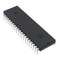


 工商网监
湘ICP备2023018690号
工商网监
湘ICP备2023018690号
