PIC18(L)F67K40
64-Pin, Low-Power, High-Performance Microcontrollers
with XLP Technology
Description
These PIC18(L)F67K40 microcontrollers feature Analog, Core Independent Peripherals and
Communication Peripherals, combined with eXtreme Low-Power (XLP) technology for a wide range of
general purpose and low-power applications. These 64-pin devices are equipped with a 10-bit ADC with
Computation (ADCC) automating Capacitive Voltage Divider (CVD) techniques for advanced touch
sensing, averaging, filtering, oversampling and performing automatic threshold comparisons. They also
offer a set of Core Independent Peripherals such as Complementary Waveform Generator (CWG),
Windowed Watchdog Timer (WWDT), Cyclic Redundancy Check (CRC)/Memory Scan, Zero-Cross
Detect (ZCD) and Peripheral Pin Select (PPS), providing for increased design flexibility and lower system
cost.
Core Features
•
•
•
•
•
•
•
•
•
•
•
C Compiler Optimized RISC Architecture
Operating Speed:
– DC – 64 MHz clock input over the full VDD range
– 62.5 ns minimum instruction cycle
Programmable 2-Level Interrupt Priority
31-Level Deep Hardware Stack
Four 8-Bit Timers (TMR2/4/6/7) with Hardware Limit Timer (HLT)
Five 16-Bit Timers (TMR0/1/3/5/7)
Low-Current Power-on Reset (POR)
Power-up Timer (PWRT)
Brown-out Reset (BOR)
Low-Power BOR (LPBOR) Option
Windowed Watchdog Timer (WWDT):
– Watchdog Reset on too long or too short interval between watchdog clear events
– Variable prescaler selection
– Variable window size selection
– All sources configurable in hardware or software
Memory
•
•
128k bytes Program Flash Memory
3562 Bytes Data SRAM Memory
© 2017 Microchip Technology Inc.
Datasheet
DS40001841D-page 1
�PIC18(L)F67K40
•
•
•
1024 Bytes Data EEPROM
Programmable Code Protection
Direct, Indirect and Relative Addressing modes
Operating Characteristics
•
•
Operating Voltage Ranges:
– 1.8V to 3.6V (PIC18LF67K40 )
– 2.3V to 5.5V ( PIC18F67K40)
Temperature Range:
– Industrial: -40°C to 85°C
– Extended: -40°C to 125°C
Power-Saving Operation Modes
•
•
•
•
•
Doze: CPU and Peripherals Running at Different Cycle Rates (typically CPU is lower)
Idle: CPU Halted While Peripherals Operate
Sleep: Lowest Power Consumption
Peripheral Module Disable (PMD):
– Ability to selectively disable hardware module to minimize active power consumption of unused
peripherals
Extreme Low-Power mode (XLP)
– Sleep: 500 nA typical @ 1.8V
– Sleep and Watchdog Timer: 900 nA typical @ 1.8V
eXtreme Low-Power (XLP) Features
•
•
•
•
Sleep mode: 50 nA @ 1.8V, typical
Windowed Watchdog Timer: 500 nA @ 1.8V, typical
Secondary Oscillator: 500 nA @ 32 kHz
Operating Current:
– 8 uA @ 32 kHz, 1.8V, typical
– 32 uA/MHz @ 1.8V, typical
Digital Peripherals
•
•
•
Complementary Waveform Generator (CWG):
– Rising and falling edge dead-band control
– Full-bridge, half-bridge, 1-channel drive
– Multiple signal sources
Capture/Compare/PWM (CCP) modules:
– Five CCPs
– 16-bit resolution for Capture/Compare modes
– 10-bit resolution for PWM mode
10-Bit Pulse-Width Modulators (PWM):
© 2017 Microchip Technology Inc.
Datasheet
DS40001841D-page 2
�PIC18(L)F67K40
•
•
•
•
•
•
•
– Two 10-bit PWMs
Serial Communications:
– Five Enhanced USART (EUSART) with Auto-Baud Detect, Auto-wake-up on Start.
RS-232, RS-485, LIN compatible
– SPI
– I2C, SMBus and PMBus™ compatible
Up to 59 I/O Pins and One Input Pin:
– Individually programmable pull-ups
– Slew rate control
– Interrupt-on-change
– Input level selection control
Programmable CRC with Memory Scan:
– Reliable data/program memory monitoring for Fail-Safe operation (e.g., Class B)
– Calculate CRC over any portion of Flash or EEPROM
– High-speed or background operation
Hardware Limit Timer (TMR2/4/6/8+HLT):
– Hardware monitoring and Fault detection
Peripheral Pin Select (PPS):
– Enables pin mapping of digital I/O
Data Signal Modulator (DSM)
Two Signal Measurement Timer (SMT1/2):
– 24-bit timer/counter with prescaler
– Multiple gate and clock inputs
Analog Peripherals
•
•
•
•
10-Bit Analog-to-Digital Converter with Computation (ADC2):
– 47 external channels
– Conversion available during Sleep
– Four internal analog channels
– Internal and external trigger options
– Automated math functions on input signals:
• Averaging, filter calculations, oversampling and threshold comparison
– 8-bit hardware acquisition timer
Hardware Capacitive Voltage Divider (CVD) Support:
– 8-bit precharge timer
– Adjustable sample and hold capacitor array
– Guard ring digital output drive
Zero-Cross Detect (ZCD):
– Detect when AC signal on pin crosses ground
5-Bit Digital-to-Analog Converter (DAC):
– Output available externally
– Programmable 5-bit voltage (% of VDD,[VRef+ - VRef-], FVR)
– Internal connections to Comparators and ADC
© 2017 Microchip Technology Inc.
Datasheet
DS40001841D-page 3
�PIC18(L)F67K40
•
•
Three Comparators (CMP):
– Five external inputs
– External output via PPS
Fixed Voltage Reference (FVR) module:
– 1.024V, 2.048V and 4.096V output levels
– Two buffered outputs: One for DAC/CMP and one for ADC
Clocking Structure
•
•
•
•
•
•
High-Precision Internal Oscillator Block (HFINTOSC):
– Selectable frequencies up to 64 MHz
– ±1% at calibration
32 kHz Low-Power Internal Oscillator (LFINTOSC)
External 32 kHz Crystal Oscillator (SOSC)
External High-frequency Oscillator Block:
– Three crystal/resonator modes
– Digital Clock Input mode
– 4x PLL with external sources
Fail-Safe Clock Monitor:
– Allows for safe shutdown if external clock stops
Oscillator Start-up Timer (OST)
Programming/Debug Features
•
•
•
In-Circuit Serial Programming™ (ICSP™) via Two Pins
In-Circuit Debug (ICD) with Three Breakpoints via Two Pins
Debug Integrated On-Chip
PIC18(L)F67K40 Family Types
© 2017 Microchip Technology Inc.
Datasheet
Debug(1)
Y
Temperature Indicator
4
Peripheral Module Disable
1
PPS
2
I2C/SPI
1
EUSART
5/2
CRC with Memory Scan
1
Timer
8-bit TMR with HLT
1
Windowed Watchdog
Low Voltage Detect (LVD)
47
SMT
3
CWG
5
CCP/10-bit PWM
60
Zero-Cross Detect
Comparators
1024
5-bit DAC
16-bit Timers
3568
Computation (ch)
I/O Pins
128k
10-bit ADC2 with
Data EEPROM
(bytes)
PIC18(L)F67K40
Data SRAM
(bytes)
Device
Program Memory Flash
(bytes)
Table 1. Devices included in this data sheet
Y
5
2
Y
Y
Y
I
DS40001841D-page 4
�PIC18(L)F67K40
16-bit Timers
Comparators
5-bit DAC
Zero-Cross Detect
CCP/10-bit PWM
CWG
SMT
Low Voltage Detect (LVD)
8-bit TMR with HLT
CRC with Memory Scan
EUSART
I2C/SPI
PPS
Peripheral Module Disable
Temperature Indicator
Debug(1)
256
25
4
2
24
1
1
2/2
1
0
1
3
Y
Y
1
1
Y
Y
Y
I
PIC18(L)F25K40
32k
2048
256
25
4
2
24
1
1
2/2
1
0
1
3
Y
Y
1
1
Y
Y
Y
I
PIC18(L)F26K40
64k
3615
1024
25
4
2
24
1
1
2/2
1
0
1
3
Y
Y
2
2
Y
Y
Y
I
PIC18(L)F27K40
128k
3615
1024
25
4
2
24
1
1
2/2
1
0
1
3
Y
Y
2
2
Y
Y
Y
I
PIC18(L)F45K40
32k
2048
256
36
4
2
35
1
1
2/2
1
0
1
3
Y
Y
2
2
Y
Y
Y
I
PIC18(L)F46K40
64k
3615
1024
36
4
2
35
1
1
2/2
1
0
1
3
Y
Y
2
2
Y
Y
Y
I
PIC18(L)F47K40
128k
3615
1024
36
4
2
35
1
1
2/2
1
0
1
3
Y
Y
2
2
Y
Y
Y
I
PIC18(L)F65K40
32k
2048
1024
60
5
3
45
1
1
5/2
1
2
1
4
Y
Y
5
2
Y
Y
Y
I
PIC18(L)F66K40
64k
3562
1024
60
5
3
45
1
1
5/2
1
2
1
4
Y
Y
5
2
Y
Y
Y
I
Timer
I/O Pins
1024
Windowed Watchdog
Data EEPROM
(bytes)
16k
Computation (ch)
Data SRAM
(bytes)
PIC18(L)F24K40
Device
10-bit ADC2 with
Program Memory Flash
(bytes)
Table 2. Devices not included in this data sheet
Note: Debugging Methods: (I) – Integrated on Chip.
Data Sheet Index:
1.
2.
3.
4.
5.
DS40001843 PIC18(L)F24/25K40 Data Sheet, 28-Pin, 8-bit Flash Microcontrollers
DS40001816 PIC18(L)F26/45/46K40 Data Sheet, 28/40/44-Pin, 8-bit Flash Microcontrollers
DS40001844 PIC18(L)F27/47K40 Data Sheet, 28/40/44-Pin, 8-bit Flash Microcontrollers
DS40001842 PIC18(L)F65/66K40 Data Sheet, 64-Pin, 8-bit Flash Microcontrollers
DS40001841 PIC18(L)F67K40 Data Sheet, 64-Pin, 8-bit Flash Microcontrollers
© 2017 Microchip Technology Inc.
Datasheet
DS40001841D-page 5
�Filename:
Title:
Last Edit:
First Used:
Notes:
Pin Diagrams
PIC18(L)F67K40
00-000064A.vsd
64-pin TQFP
3/6/2017
N/A
Generic 64-pin TQFP diagram
Figure 1. 64-pin TQFP
RE2
RE3
RE4
RE5
RE6
RE7
RD0
RH2
RH3
RD1
RD2
RD3
RD4
RD5
RD6
RD7
Rev. 00-000 064A
3/6/201 7
64 63 62 61 60 59 58 57 56 55 54 53 52 51 50 49
RE1
RE0
RG0
RG1
RG2
RG3
VPP /MCLR/RG5
RG4
VSS
VDD
RF7
RF6
RF5
RF4
RF3
RF2
1
48
2
47
3
46
4
45
5
44
6
43
7
42
8
41
9
40
10
39
11
38
12
37
13
36
14
35
15
34
16
33
RB0
RB1
RB2
RB3
RB4
RB5
RB6
VSS
RA6
RA7
VDD
RB7
RC5
RC4
RC3
RC2
RF1
RF0
RG7
RG6
RA3
RA2
RA1
RA0
RH1
RH0
RA5
RA4
RC1
RC0
RC6
RC7
17 18 19 20 21 22 23 24 25 26 27 28 29 30 31 32
© 2017 Microchip Technology Inc.
Datasheet
DS40001841D-page 6
�Filename:
Title:
Last Edit:
First Used:
Notes:
00-000064B.vsd
64-pin QFN
3/7/2017
N/A
Generic 64-pin QFN diagram
PIC18(L)F67K40
Figure 2. 64-pin QFN
RE2
RE3
RE4
RE5
RE6
RE7
RD0
RH2
RH3
RD1
RD2
RD3
RD4
RD5
RD6
RD7
Rev. 00-000 064B
3/7/201 7
64 63 62 61 60 59 58 57 56 55 54 53 52 51 50 49
RE1
RE0
RG0
RG1
RG2
RG3
VPP /MCLR/RG5
RG4
VSS
VDD
RF7
RF6
RF5
RF4
RF3
RF2
1
48
2
47
3
46
4
45
5
44
6
43
7
42
8
41
9
40
10
39
11
12
38
37
13
36
14
35
15
34
33
16
RB0
RB1
RB2
RB3
RB4
RB5
RB6
VSS
RA6
RA7
VDD
RB7
RC5
RC4
RC3
RC2
RF1
RF0
RG7
RG6
RA3
RA2
RA1
RA0
RH1
RH0
RA5
RA4
RC1
RC0
RC6
RC7
17 18 19 20 21 22 23 24 25 26 27 28 29 30 31 32
Note: It is recommended that the exposed bottom pad be connected to VSS, however it must not be the only
VSS connection to the device.
Pin Allocation Tables
Table 1. 64-Pin Allocation Table
I/O(2)
RA0
64Pin
TQFP,
QFN
A/D
DAC
24
ANA0
—
C1IN4-
Clock
Reference Interrupt EUSART
(CLKR)
CCP and
PWM
CWG
ZCD
SMT
T8IN(1)
—
—
—
—
—
Comparator Timers
DSM
MSSP
Basic
—
—
—
—
C2IN4C3IN4RA1
23
ANA1
—
—
T2IN(1)
—
—
—
—
—
—
—
—
—
—
RA2
22
ANA2
Vref-
C1IN1+
—
—
—
—
—
—
—
—
—
—
—
Vref-
C2IN1+
C3IN1+
RA3
21
ANA3
Vref+
—
—
—
—
—
—
—
—
—
—
—
—
—
—
T0CKI(1)
—
—
—
—
—
—
—
—
—
—
Vref+
RA4
28
ANA4
RA5
27
ANA5
—
—
T3G(1)
—
—
—
—
—
—
—
—
—
—
RA6
40
ANA6
—
—
—
—
—
—
—
—
—
—
—
—
CLKOUT
RA7
39
ANA7
—
—
—
—
—
—
—
—
—
—
—
OSC2
© 2017 Microchip Technology Inc.
Datasheet
DS40001841D-page 7
OSC1
�PIC18(L)F67K40
I/O(2)
64Pin
TQFP,
QFN
A/D
DAC
Comparator Timers
CCP and
PWM
CWG
ZCD
SMT
Clock
Reference Interrupt EUSART
(CLKR)
DSM
MSSP
Basic
CLKIN
RB0
48
ANB0
—
—
—
—
—
ZCDIN
—
—
IOCB0
—
—
—
—
—
—(4)
—
—
—
—(4)
—
—
—
—
—
INT0(1)
RB1
47
ANB1
—
—
—
—
—
—
—
—
IOCB1
INT1(1)
RB2
46
ANB2
—
—
—
—
—
—
—
—
IOCB2
INT2(1)
RB3
45
ANB3
—
—
—
—
—
—
—
—
IOCB3
INT3(1)
RB4
RB5
44
43
ANB4
ANB5
—
—
—
—
—
—
—
—
—
IOCB4
—
—
—
—
—
T1G(1)
—
—
—
—
—
IOCB5
—
—
—
—
—
—
—
—
—
—
IOCB6
—
—
—
ICSPCLK
—
T3CKI(1)
RB6
42
ANB6
—
—
RB7
37
ANB7
DAC1OUT2
—
—
—
—
—
—
—
IOCB7
—
—
ICSPDAT
RC0
30
—
—
—
T1CKI(1)
—
—
—
—
—
IOCC0 CK4(1,3)
—
—
SOSCO
—
IOCC1 RX4(1,3)
DT4(1,3)
—
—
SOSCI
—
IOCC2
—
—
—
—
RC1
29
—
—
—
T6IN(1)
RC2
33
—
—
—
—
—
—
—
CWG1IN(1)
—
—
—
RC3
34
—
—
—
—
—
—
—
—
—
IOCC3
—
—
SCL1(3,4)
SCK1(1)
RC4
35
—
—
—
—
—
—
—
—
—
IOCC4
—
—
SDA1(3,4)
SDI1(1)
—
RC5
36
—
—
—
—
—
—
—
—
—
IOCC5
—
—
—
—
RC6
31
—
—
—
—
—
—
—
—
—
IOCC6 CK1(1,3)
—
—
—
IOCC7 RX1(1,3)
DT1(1,3)
—
—
—
RC7
32
—
—
—
—
—
—
—
—
—
RD0
58
AND0
—
—
—
—
—
—
—
—
—
—
—
—
—
—
—
—
—
—
—
—
—
—
—
RD1
55
AND1
—
—
T5CKI(1)
T7G(1)
RD2
54
AND2
—
—
—
—
—
—
—
—
—
—
—
—
—
RD3
53
AND3
—
—
—
—
—
—
—
—
—
—
MDCARL(1)
—
—
—
MDCARH(1)
—
RD4
52
AND4
—
—
—
—
—
—
—
—
—
MDSRC(1) SDA2(3,4)
SDI2(1)
RD5
51
AND5
—
—
—
—
—
—
—
—
—
—
—
RD6
50
AND6
—
—
—
—
—
—
—
—
—
—
—
SCL2(3,4)
SCK2(1)
RD7
49
AND7
—
—
—
—
—
—
—
—
—
—
—
SS2(1)
—
RE0
2
ANE0
—
—
—
—
—
—
—
—
IOCE0 CK3(1,3)
—
—
—
RE1
1
ANE1
—
—
—
—
—
—
—
—
IOCE1 RX3(1,3)
DT3(1,3)
—
—
—
RE2
64
ANE2
—
—
—
—
—
—
—
—
IOCE2 CK5(1,3)
—
—
—
—
—
—
RE3
63
ANE3
—
—
—
—
—
—
—
—
IOCE3 RX5(1,3)
DT5(1,3)
RE4
62
ANE4
—
—
T4IN(1)
CCP2(1)
—
—
—
—
IOCE4
—
—
—
—
RE5
61
ANE5
—
—
—
CCP1(1)
—
—
—
—
IOCE5
—
—
—
—
RE6
60
ANE6
—
—
—
CCP3(1)
—
—
SMT1WIN1(1)
—
IOCE6
—
—
—
—
© 2017 Microchip Technology Inc.
Datasheet
DS40001841D-page 8
�PIC18(L)F67K40
64Pin
TQFP,
QFN
A/D
DAC
RE7
59
ANE7
—
—
RF0
18
ANF0
—
RF1
17
ANF1
RF2
16
ANF2
RF3
15
ANF3
RF4
14
RF5
13
RF6
RF7
Clock
Reference Interrupt EUSART
(CLKR)
CCP and
PWM
CWG
ZCD
SMT
—
—
—
—
SMT1SIG1(1)
—
IOCE7
C1IN0C2IN0-
—
—
—
—
—
—
—
—
—
—
—
—
—
—
—
—
—
—
—
—
—
C1IN2C2IN2C3IN2-
—
—
—
—
ANF4
—
C2IN0+
—
—
—
ANF5
DAC1OUT1
C1IN1C2IN1-
—
—
—
12
ANF6
—
C1IN0+
—
—
11
ANF7
—
C2IN3C1IN3C3IN3-
—
—
RG0
3
ANG0
—
—
—
RG1
4
ANG1
—
—
—
RG2
5
ANG2
—
C3IN0+
—
RG3
6
ANG3
—
C3IN0-
RG4
8
ANG4
—
C3IN1-
RG5
7
—
—
—
—
RG6
20
ANG6
—
—
RG7
19
ANG7
—
—
RH0
26
—
—
RH1
25
ADCACT(1)
RH2
57
RH3
I/O(2)
DSM
MSSP
Basic
—
—
—
—
—
—
—
—
—
—
—
—
—
—
—
—
—
—
—
—
—
—
—
—
—
—
—
—
—
—
—
—
—
—
—
—
—
—
—
—
—
—
—
—
—
—
—
—
—
—
—
—
—
—
—
—
—
—
—
—
SS1(1)
—
—
—
—
—
—
—
—
—
—
—
—
—
—
—
—
—
—
—
—
—
—
—
—
—
—
CK2(1,3)
RX2(1,3)
DT2(1,3)
—
—
—
—
—
—
—
—
—
—
—
—
—
—
—
—
—
—
—
—
—
—
—
—
—
—
IOCG5
—
—
—
Vpp/
MCLR
—
—
—
—
—
—
—
—
—
—
—
—
SMT2WIN1(1)
SMT2SIG1(1)
—
—
—
—
—
—
—
—
—
—
—
—
—
—
—
—
—
—
—
—
—
—
—
—
—
—
—
—
—
—
—
—
—
—
—
—
—
—
—
—
—
—
—
—
—
—
—
56
—
—
—
—
—
—
—
—
—
—
—
—
—
—
VDD
10, 38
—
—
—
—
—
—
—
—
—
—
—
—
—
VDD
VSS
9, 41
—
—
—
—
—
—
—
—
—
—
—
—
—
VSS
—
ADGRDA
ADGRDB
—
C1OUT
C2OUT
C3OUT
TMR0
CCP1
CCP2
CWG1A
CWG1B
—
—
CLKR
—
DSM
SDO1
SCK1
—
CCP3
CWG1C
CCP4
CWG1D
TX1/
CK1(3)
DT1(3)
TX2/
CK2(3)
DT2(3)
OUT(2)
Comparator Timers
—
CCP4(1)
(1)
T5G
CCP5(1)
T7CKI(1)
CCP5
SDO2
SCK2
TX3/
CK3(3)
DT3(3)
TX4/
CK4(3)
DT4(3)
PWM6OUT
PWM7OUT
TX5/
CK5(3)
DT5(3)
Note:
1.
This is a PPS remappable input signal. The input function may be moved from the default location shown to one of several other PORTx pins. Refer to the
peripheral input selection table for details on which PORT pins may be used for this signal.
2.
All output signals shown in this row are PPS remappable. These signals may be mapped to output onto one of several PORTx pin options as described in the
peripheral output selection table.
3.
This is a bidirectional signal. For normal module operation, the firmware should map this signal to the same pin in both the PPS input and PPS output registers.
These pins are configured for I2C logic levels; The SCLx/SDAx signals may be assigned to any of these pins. PPS assignments to the other pins (e.g., RB1) will
operate, but input logic levels will be standard TTL/ST as selected by the INLVL register, instead of the I2C specific or SMBus input buffer thresholds.
4.
© 2017 Microchip Technology Inc.
Datasheet
DS40001841D-page 9
�PIC18(L)F67K40
Table of Contents
Description.......................................................................................................................1
Core Features................................................................................................................ 1
Memory...........................................................................................................................1
Operating Characteristics.............................................................................................2
Power-Saving Operation Modes......................................................................................2
eXtreme Low-Power (XLP) Features............................................................................2
Digital Peripherals......................................................................................................... 2
Analog Peripherals........................................................................................................3
Clocking Structure........................................................................................................ 4
Programming/Debug Features..................................................................................... 4
PIC18(L)F67K40 Family Types......................................................................................4
Pin Diagrams..................................................................................................................6
Pin Allocation Tables.................................................................................................... 7
1. Device Overview......................................................................................................13
2. Guidelines for Getting Started with PIC18(L)F67K40 Microcontrollers................... 20
3. Device Configuration............................................................................................... 25
4. Oscillator Module (with Fail-Safe Clock Monitor).....................................................41
5. Reference Clock Output Module............................................................................. 64
6. Power-Saving Operation Modes..............................................................................70
7. (PMD) Peripheral Module Disable........................................................................... 80
8. Resets..................................................................................................................... 92
9. (WWDT) Windowed Watchdog Timer....................................................................104
10. Memory Organization............................................................................................ 116
11. (NVM) Nonvolatile Memory Control.......................................................................151
© 2017 Microchip Technology Inc.
Datasheet
DS40001841D-page 10
�PIC18(L)F67K40
12. 8x8 Hardware Multiplier.........................................................................................178
13. Cyclic Redundancy Check (CRC) Module with Memory Scanner.........................183
14. Interrupts............................................................................................................... 203
15. I/O Ports................................................................................................................ 244
16. Interrupt-on-Change.............................................................................................. 313
17. (PPS) Peripheral Pin Select Module......................................................................329
18. Resets................................................................................................................... 341
19. Timer0 Module.......................................................................................................353
20. Timer1 Module with Gate Control.......................................................................... 362
21. Timer2 Module.......................................................................................................383
22. Capture/Compare/PWM Module........................................................................... 410
23. (PWM) Pulse-Width Modulation............................................................................ 427
24. (ZCD) Zero-Cross Detection Module.....................................................................437
25. (CWG) Complementary Waveform Generator Module..........................................445
26. (SMT) Signal Measurement Timer.........................................................................474
27. (DSM) Data Signal Modulator Module...................................................................501
28. (MSSP) Master Synchronous Serial Port Module................................................. 515
29. (EUSART) Enhanced Universal Synchronous Asynchronous Receiver Transmitter
...............................................................................................................................580
30. (FVR) Fixed Voltage Reference.............................................................................615
31. Temperature Indicator Module...............................................................................620
32. (DAC) 5-Bit Digital-to-Analog Converter Module................................................... 623
33. (ADC2) Analog-to-Digital Converter with Computation Module............................. 629
34. (CMP) Comparator Module................................................................................... 678
35. (HLVD) High/Low-Voltage Detect.......................................................................... 691
36. Register Summary.................................................................................................699
37. In-Circuit Serial Programming™ (ICSP™) .............................................................711
© 2017 Microchip Technology Inc.
Datasheet
DS40001841D-page 11
�PIC18(L)F67K40
38. Instruction Set Summary....................................................................................... 714
39. Development Support............................................................................................808
40. Electrical Specifications.........................................................................................813
41. DC and AC Characteristics Graphs and Tables.................................................... 847
42. Packaging Information...........................................................................................867
43. Revision History.....................................................................................................874
The Microchip Web Site.............................................................................................. 875
Customer Change Notification Service........................................................................875
Customer Support....................................................................................................... 875
Product Identification System...................................................................................... 876
Microchip Devices Code Protection Feature............................................................... 876
Legal Notice.................................................................................................................877
Trademarks................................................................................................................. 877
Quality Management System Certified by DNV...........................................................878
Worldwide Sales and Service......................................................................................879
© 2017 Microchip Technology Inc.
Datasheet
DS40001841D-page 12
�PIC18(L)F67K40
Device Overview
1.
Device Overview
This document contains device specific information for the following devices:
•
PIC18F67K40
•
PIC18LF67K40
This family offers the advantages of all PIC18 microcontrollers – namely, high computational performance
at an economical price – with the addition of high-endurance Program Flash Memory. In addition to these
features, the PIC18(L)F67K40 family introduces design enhancements that make these microcontrollers
a logical choice for many high-performance, power sensitive applications.
1.1
New Core Features
1.1.1
XLP Technology
All of the devices in the PIC18(L)F67K40 family incorporate a range of features that can significantly
reduce power consumption during operation. Key items include:
•
•
•
•
1.1.2
Alternate Run Modes: By clocking the controller from the secondary oscillator or the internal
oscillator block, power consumption during code execution can be reduced by as much as 90%.
Multiple Idle Modes: The controller can also run with its CPU core disabled but the peripherals still
active. In these states, power consumption can be reduced even further, to as little as 4% of normal
operation requirements.
On-the-fly Mode Switching: The power-managed modes are invoked by user code during operation,
allowing the user to incorporate power-saving ideas into their application’s software design.
Peripheral Module Disable: Modules that are not being used in the code can be selectively disabled
using the PMD module. This further reduces the power consumption.
Multiple Oscillator Options and Features
All of the devices in the PIC18(L)F67K40family offer several different oscillator options. The
PIC18(L)F67K40 family can be clocked from several different sources:
•
•
•
•
•
•
HFINTOSC
– 1-64 MHz precision digitally controlled internal oscillator
LFINTOSC
– 31 kHz internal oscillator
EXTOSC
– External clock (EC)
– Low-power oscillator (LP)
– Medium-power oscillator (XT)
– High-power oscillator (HS)
SOSC
– Secondary oscillator circuit optimized for 32 kHz clock crystals
A Phase Lock Loop (PLL) frequency multiplier (4x) is available to the External Oscillator modes
enabling clock speeds of up to 64 MHz
Fail-Safe Clock Monitor: This option constantly monitors the main clock source against a reference
signal provided by the LFINTOSC. If a clock failure occurs, the controller is switched to the internal
oscillator block, allowing for continued operation or a safe application shutdown.
© 2017 Microchip Technology Inc.
Datasheet
DS40001841D-page 13
�PIC18(L)F67K40
Device Overview
1.2
Other Special Features
•
•
•
•
•
•
•
1.3
Memory Endurance: The Flash cells for both program memory and data EEPROM are rated to last
for many thousands of erase/write cycles – up to 10K for program memory and 100K for EEPROM.
Data retention without refresh is conservatively estimated to be greater than 40 years.
Self-programmability: These devices can write to their own program memory spaces under internal
software control. By using a boot loader routine located in the protected Boot Block at the top of
program memory, it becomes possible to create an application that can update itself in the field.
Extended Instruction Set: The PIC18(L)F67K40 family includes an optional extension to the PIC18
instruction set, which adds eight new instructions and an Indexed Addressing mode. This
extension, enabled as a device configuration option, has been specifically designed to optimize reentrant application code originally developed in high-level languages, such as C.
Enhanced Peripheral Pin Select: The Peripheral Pin Select (PPS) module connects peripheral
inputs and outputs to the device I/O pins. Only digital signals are included in the selections. All
analog inputs and outputs remain fixed to their assigned pins.
Enhanced Addressable EUSART: This serial communication module is capable of standard
RS-232 operation and provides support for the LIN bus protocol. Other enhancements include
automatic baud rate detection and a 16-bit Baud Rate Generator for improved resolution. When the
microcontroller is using the internal oscillator block, the EUSART provides stable operation for
applications that talk to the outside world without using an external crystal (or its accompanying
power requirement).
10-bit A/D Converter with Computation: This module incorporates programmable acquisition time,
allowing for a channel to be selected and a conversion to be initiated without waiting for a sampling
period and thus, reduce code overhead. It has a new module called ADC2 with computation
features, which provides a digital filter and threshold interrupt functions.
Windowed Watchdog Timer (WWDT):
– Timer monitoring of overflow and underflow events
– Variable prescaler selection
– Variable window size selection
– All sources configurable in hardware or software
Details on Individual Family Members
Devices in the PIC18(L)F67K40 family are available in 64-pin packages. The block diagram for this
device is shown in Figure 1-1.
The devices have the following differences:
1.
2.
3.
4.
5.
6.
7.
Program Flash Memory
Data Memory SRAM
Data Memory EEPROM
A/D channels
I/O ports
Enhanced USART
Input Voltage Range/Power Consumption
All other features for devices in this family are identical. These are summarized in the following Device
Features table.
© 2017 Microchip Technology Inc.
Datasheet
DS40001841D-page 14
�PIC18(L)F67K40
Device Overview
The pinouts for all devices are listed in the pin summary tables.
Table 1-1. Device Features
Features
PIC18(L)F67K40
Program Memory (Bytes)
131072
Program Memory (Instructions)
65536
Data Memory (Bytes)
3562
Data EEPROM Memory (Bytes)
1024
A,B,C,D,E,F,G(1),H
I/O Ports
Capture/Compare/PWM Modules (CCP)
5
10-Bit Pulse-Width Modulator (PWM)
2
10-Bit Analog-to-Digital Module (ADC2) with Computation
Accelerator
4 internal
47 external
64-pin TQFP
64-pin QFN
Packages
Interrupt Sources
56
Timers (16-/8-bit)
5/4
2 MSSP,
5 EUSART
Serial Communications
Enhanced Complementary Waveform Generator (ECWG)
1
Signal Measurement Timer (SMT)
2
Comparators
3
Zero-Cross Detect (ZCD)
1
Data Signal Modulator (DSM)
1
Peripheral Pin Select (PPS)
Yes
Peripheral Module Disable (PMD)
Yes
16-bit CRC with NVMSCAN
Yes
Programmable High/Low-Voltage Detect (HLVD)
Yes
Programmable Brown-out Reset (BOR)
Yes
POR, BOR,
RESET Instruction,
Stack Overflow,
Resets (and Delays)
Stack Underflow,
MCLR, WWDT,
(PWRT, OST)
© 2017 Microchip Technology Inc.
Datasheet
DS40001841D-page 15
�PIC18(L)F67K40
Device Overview
Features
PIC18(L)F67K40
75 Instructions;
83 with Extended Instruction Set enabled
Instruction Set
Operating Frequency
DC – 64 MHz
Note 1: RG5 is an input only pin.
© 2017 Microchip Technology Inc.
Datasheet
DS40001841D-page 16
�PIC18(L)F67K40
Device Overview
Figure 1-1. PIC18(L)F67K40 Family Block Diagram
Rev. 30-000131C
6/14/2017
Data Bus
Table Pointer
Data Latch
8
8
inc/dec logic
PORTA
RA
Data Memory
PCLATU PCLATH
21
Address Latch
20
PCU PCH PCL
Program Counter
31-Level Stack
4
BSR
Address Latch
Program Memory
(8/16/32/64 Kbytes)
12
Data Address
STKPTR
12
FSR0
FSR1
FSR2
Data Latch
8
4
Access
Bank
PORTC
12
RC
inc/dec
logic
Table Latch
PORTD
Address
Decode
ROM Latch
Instruction Bus
PORTB
RB
RD
IR
8
State machine
control signals
Instruction
Decode and
Control
PRODH PRODL
8x8 Multiply
3
8
W
BITOP
8
Internal
Oscillator
Block
Power-up
Timer
SOSCI
LFINTOSC
Oscillator
SOSCO
64 MHz
Oscillator
Oscillator
Start-up Timer
Power-on
Reset
OSC1(1)
OSC2
(1)
BOR
HLVD
FVR
Comparators
DAC
C1/C2/C3
Note
1:
Timer0
Timer1
Timer3
Timer5
Timer7
Timer2
Timer4
Timer6
Timer8
CCP1
CCP2
CCP3
CCP4
CCP5
PWM6
PWM7
MSSP1
MSSP2
EUSART1
EUSART2
EUSART3
EUSART4
EUSART5
8
PORTG
RG
8
Precision
Band Gap
Reference
ZCD
FVR
PORTH
RH
CRC-Scan
SMT1
SMT2
DSM
PMD
ECWG
PORTF
RF
8
ALU
Brown-out
Reset
Fail-Safe
Clock Monitor
NVM
Controller
8
8
Watchdog
Timer
Single-Supply
Programming
In-Circuit
Debugger
MCLR
PORTE
RE
DAC
ADC
10-bit
FVR
FVR
OSC1/CLKIN and OSC2/CLKOUT are only available in select oscillator modes.
© 2017 Microchip Technology Inc.
Datasheet
DS40001841D-page 17
�PIC18(L)F67K40
Device Overview
1.4
Register and Bit naming conventions
1.4.1
Register Names
When there are multiple instances of the same peripheral in a device, the peripheral control registers will
be depicted as the concatenation of a peripheral identifier, peripheral instance, and control identifier. The
control registers section will show just one instance of all the register names with an ‘x’ in the place of the
peripheral instance number. This naming convention may also be applied to peripherals when there is
only one instance of that peripheral in the device to maintain compatibility with other devices in the family
that contain more than one.
1.4.2
Bit Names
There are two variants for bit names:
•
•
1.4.2.1
Short name: Bit function abbreviation
Long name: Peripheral abbreviation + short name
Short Bit Names
Short bit names are an abbreviation for the bit function. For example, some peripherals are enabled with
the EN bit. The bit names shown in the registers are the short name variant.
Short bit names are useful when accessing bits in C programs. The general format for accessing bits by
the short name is RegisterNamebits.ShortName. For example, the enable bit, EN, in the CM1CON0
register can be set in C programs with the instruction CM1CON0bits.EN = 1.
Short names are generally not useful in assembly programs because the same name may be used by
different peripherals in different bit positions. When this occurs, during the include file generation, all
instances of that short bit name are appended with an underscore plus the name of the register in which
the bit resides to avoid naming contentions.
1.4.2.2
Long Bit Names
Long bit names are constructed by adding a peripheral abbreviation prefix to the short name. The prefix is
unique to the peripheral thereby making every long bit name unique. The long bit name for the COG1
enable bit is the COG1 prefix, G1, appended with the enable bit short name, EN, resulting in the unique
bit name G1EN.
Long bit names are useful in both C and assembly programs. For example, in C the COG1CON0 enable
bit can be set with the G1EN = 1 instruction. In assembly, this bit can be set with the BSF
COG1CON0,G1EN instruction.
1.4.2.3
Bit Fields
Bit fields are two or more adjacent bits in the same register. Bit fields adhere only to the short bit naming
convention. For example, the three Least Significant bits of the COG1CON0 register contain the mode
control bits. The short name for this field is MD. There is no long bit name variant. Bit field access is only
possible in C programs. The following example demonstrates a C program instruction for setting the
COG1 to the Push-Pull mode:
COG1CON0bits.MD = 0x5;
Individual bits in a bit field can also be accessed with long and short bit names. Each bit is the field name
appended with the number of the bit position within the field. For example, the Most Significant mode bit
has the short bit name MD2 and the long bit name is G1MD2. The following two examples demonstrate
assembly program sequences for setting the COG1 to Push-Pull mode:
© 2017 Microchip Technology Inc.
Datasheet
DS40001841D-page 18
�PIC18(L)F67K40
Device Overview
Example 1:
MOVLW
ANDWF
MOVLW
IORWF
~(1 PRODH:PRODL
8x8 Signed Multiply Routine
MOVF
MULWF
BTFSC
SUBWF
MOVF
BTFSC
SUBWF
ARG1, W
ARG2
ARG2, SB
PRODH, F
ARG2, W
ARG1, SB
PRODH, F
; ARG1 * ARG2 -> PRODH:PRODL
; Test Sign Bit
; PRODH = PRODH - ARG1
; Test Sign Bit
; PRODH = PRODH - ARG2
Table 12-1. Performance Comparison for Various Multiply Operations
Routine
8x8 unsigned
Multiply Method
Program
Time
Cycles
Memory
(Max) @ 64 MHz @ 40 MHz @ 10 MHz @ 4 MHz
(Words)
Without hardware
multiply
13
69
4.3 μs
6.9 μs
27.6 μs
69 μs
Hardware multiply
1
1
62.5 ns
100 ns
400 ns
1 μs
© 2017 Microchip Technology Inc.
Datasheet
DS40001841D-page 178
�PIC18(L)F67K40
8x8 Hardware Multiplier
Routine
Multiply Method
Program
Time
Cycles
Memory
(Max) @ 64 MHz @ 40 MHz @ 10 MHz @ 4 MHz
(Words)
Without hardware
multiply
33
91
5.7 μs
9.1 μs
36.4 μs
91 μs
Hardware multiply
6
6
375 ns
600 ns
2.4 μs
6 μs
Without hardware
16x16 unsigned multiply
21
242
15.1 μs
24.2 μs
96.8 μs
242 μs
Hardware multiply
28
28
1.8 μs
2.8 μs
11.2 μs
28 μs
Without hardware
multiply
52
254
15.9 μs
25.4 μs
102.6 μs
254 μs
Hardware multiply
35
40
2.5 μs
4.0 μs
16.0 μs
40 μs
8x8 signed
16x16 signed
16 x 16 Unsigned Multiply Routine shows the sequence to do a 16 x 16 unsigned multiplication. The
equation below shows the algorithm that is used. The 32-bit result is stored in four registers (RES).
16 x 16 Unsigned Multiplication Algorithm
���3: ���0 = ���1�: ���1� • ���2�: ���2� = ���1� • ���2� • 216 + ���1� • ���2� • 28 +
���1� • ���2� • 28 + ���1� • ���2�
16 x 16 Unsigned Multiply Routine
;
;
;
MOVF
MULWF
MOVFF
MOVFF
ARG1L, W
ARG2L
PRODH, RES1
PRODL, RES0
; ARG1L * ARG2L → PRODH:PRODL
;
;
MOVF
MULWF
MOVFF
MOVFF
ARG1H, W
ARG2H
PRODH, RES3
PRODL, RES2
;
; ARG1H * ARG2H → PRODH:PRODL
;
;
MOVF
MULWF
MOVF
ADDWF
MOVF
ADDWFC
CLRF
ADDWFC
ARG1L, W
ARG2H
PRODL, W
RES1, F
PRODH, W
RES2, F
WREG
RES3, F
; ARG1L * ARG2H → PRODH:PRODL
;
; Add cross products
;
;
;
;
MOVF
MULWF
MOVF
ADDWF
MOVF
ADDWFC
CLRF
ADDWFC
ARG1H, W
ARG2L
PRODL, W
RES1, F
PRODH, W
RES2, F
WREG
RES3, F
;
; ARG1H * ARG2L → PRODH:PRODL
;
; Add cross products
;
;
;
;
16 x 16 Signed Multiply Routine shows the sequence to do a 16 x 16 signed multiply. The equation below
shows the algorithm used. The 32-bit result is stored in four registers (RES). To account for the sign
bits of the arguments, the MSb for each argument pair is tested and the appropriate subtractions are
done.
© 2017 Microchip Technology Inc.
Datasheet
DS40001841D-page 179
�PIC18(L)F67K40
8x8 Hardware Multiplier
16 x 16 Signed Multiplication Algorithm
���3: ���0 = ���1�: ���1� • ���2�: ���2� = ���1� • ���2� • 216 + ���1� • ���2� • 28 +
���1� • ���2� • 28 + ���1� • ���2� + − 1 • ���2� < 7 > • ���1�: ���1� • 216 + − 1
• ���1� < 7 > • ���2�: ���2� • 216
16 x 16 Signed Multiply Routine
;
;
;
;
;
MOVF
MULW
MOVF
MOVFF
ARG1L, W
ARG2L
PRODH, RES1
PRODL, RES0
; ARG1L * ARG2L → PRODH:PRODL
;
;
MOVF
MULWF
MOVFF
MOVFF
ARG1H, W
ARG2H
PRODH, RES3
PRODL, RES2
; ARG1H * ARG2H → PRODH:PRODL
;
;
MOVF
MULWF
MOVF
ADDWF
MOVF
ADDWFC
CLRF
ADDWFC
ARG1L, W
ARG2H
PRODL, W
RES1, F
PRODH, W
RES2, F
WREG
RES3, F
; ARG1L * ARG2H → PRODH:PRODL
;
; Add cross products
;
;
;
;
MOVF
MULWF
MOVF
ADDWF
MOVF
ADDWFC
CLRF
ADDWFC
ARG1H, W
ARG2L
PRODL, W
RES1, F
PRODH, W
RES2, F
WREG
RES3, F
;
; ARG1H * ARG2L → PRODH:PRODL
;
; Add cross products
;
;
;
;
BTFSS
BRA
MOVF
SUBWF
MOVF
SUBWFB
ARG2H, 7
SIGN_ARG1
ARG1L, W
RES2
ARG1H, W
RES3
; ARG2H:ARG2L neg?
; no, check ARG1
;
;
;
ARG1H, 7
CONT_CODE
ARG2L, W
RES2
ARG2H, W
RES3
; ARG1H:ARG1L neg?
; no, done
;
;
;
SIGN_ARG1:
BTFSS
BRA
MOVF
SUBWF
MOVF
SUBWFB
;
CONT_CODE:
:
© 2017 Microchip Technology Inc.
Datasheet
DS40001841D-page 180
�PIC18(L)F67K40
8x8 Hardware Multiplier
12.3
Register Summary - 8x8 Hardware Multiplier
Offset
Name
0x0FF3
PROD
12.4
Bit Pos.
7:0
PRODL[7:0]
15:8
PRODH[7:0]
Register Definitions: 8x8 Hardware Multiplier
© 2017 Microchip Technology Inc.
Datasheet
DS40001841D-page 181
�PIC18(L)F67K40
8x8 Hardware Multiplier
12.4.1
PROD
Name:
PROD
Address: 0xFF3
Product Register Pair
The PROD register stores the 16-bit result yielded by the unsigned operation performed by the 8x8
hardware multiplier.
Bit
15
14
13
12
11
10
9
8
PRODH[7:0]
Access
R/W
R/W
R/W
R/W
R/W
R/W
R/W
R/W
Reset
x
x
x
x
x
x
x
x
Bit
7
6
5
4
3
2
1
0
PRODL[7:0]
Access
Reset
R/W
R/W
R/W
R/W
R/W
R/W
R/W
R/W
x
x
x
x
x
x
x
x
Bits 15:8 – PRODH[7:0]
PROD Most Significant bits
Bits 7:0 – PRODL[7:0]
PROD Least Significant bits
© 2017 Microchip Technology Inc.
Datasheet
DS40001841D-page 182
�PIC18(L)F67K40
Cyclic Redundancy Check (CRC) Module with Me...
13.
Cyclic Redundancy Check (CRC) Module with Memory Scanner
The Cyclic Redundancy Check (CRC) module provides a software-configurable hardware-implemented
CRC checksum generator. This module includes the following features:
•
•
•
•
•
•
•
13.1
Any standard CRC up to 16 bits can be used
Configurable Polynomial
Any seed value up to 16 bits can be used
Standard and reversed bit order available
Augmented zeros can be added automatically or by the user
Memory scanner for fast CRC calculations on program memory user data
Software loadable data registers for communication CRC’s
CRC Module Overview
The CRC module provides a means for calculating a check value of program memory. The CRC module
is coupled with a memory scanner for faster CRC calculations. The memory scanner can automatically
provide data to the CRC module. The CRC module can also be operated by directly writing data to SFRs,
without using a scanner.
13.2
CRC Functional Overview
The CRC module can be used to detect bit errors in the Flash memory using the built-in memory scanner
or through user input RAM memory. The CRC module can accept up to a 16-bit polynomial with up to a
16-bit seed value. A CRC calculated check value (or checksum) will then be generated into the CRCACC
registers for user storage. The CRC module uses an XOR shift register implementation to perform the
polynomial division required for the CRC calculation.
© 2017 Microchip Technology Inc.
Datasheet
DS40001841D-page 183
�Filename:
Title:
Last Edit:
First Used:
Notes:
10-000206A.vsd
CRC EXAMPLE
1/8/2014
PIC16(L)F1613
PIC18(L)F67K40
Cyclic Redundancy Check (CRC) Module with Me...
Figure 13-1. CRC Example
Rev. 10-000206A
1/8/2014
CRC-16-ANSI
x16 + x15 + x2 + 1 (17 bits)
Standard 16-bit representation = 0x8005
CRCXORH = 0b10000000
CRCXORL = 0b0000010-
(1)
Data Sequence:
0x55, 0x66, 0x77, 0x88
DLEN = 0b0111
PLEN = 0b1111
Data entered into the CRC:
SHIFTM = 0:
01010101 01100110 01110111 10001000
SHIFTM = 1:
10101010 01100110 11101110 00010001
Check Value (ACCM = 1):
SHIFTM = 0: 0x32D6
CRCACCH = 0b00110010
CRCACCL = 0b11010110
SHIFTM = 1: 0x6BA2
CRCACCH = 0b01101011
CRCACCL = 0b10100010
Note 1: Bit 0 is unimplemented. The LSb of any
CRC polynomial is always ‘1’ and will always
be treated as a ‘1’ by the CRC for calculating
the CRC check value. This bit will be read in
software as a ‘0’.
13.3
CRC Polynomial Implementation
Any polynomial can be used. The polynomial and accumulator sizes are determined by the PLEN bits.
For an n-bit accumulator, PLEN = n-1 and the corresponding polynomial is n+1 bits. Therefore, the
accumulator can be any size up to 16 bits with a corresponding polynomial up to 17 bits. The MSb and
LSb of the polynomial are always ‘1’ which is forced by hardware. However, the LSb of the CRCXORL
register is unimplemented and always reads as '0'.
All polynomial bits between the MSb and LSb are specified by the CRCXOR registers. For example,
when using CRC16-ANSI, the polynomial is defined as X16+X15+X2+1. The X16 and X0 = 1 terms are the
MSb and LSb controlled by hardware. The X15 and X2 terms are specified by setting the corresponding
CRCXOR bits with the value of 0x8004. The actual value is 0x8005 because the hardware sets
the LSb to 1. Refer to Figure 13-1.
© 2017 Microchip Technology Inc.
Datasheet
DS40001841D-page 184
�Filename:
Title:
Last Edit:
First Used:
Notes:
10-000207A.vsd
CRC LFSR EXAMPLE
5/27/2014
PIC16F1613 LECQ
PIC18(L)F67K40
Cyclic Redundancy Check (CRC) Module with Me...
Figure 13-2. CRC LFSR Example
Rev. 10-000207A
5/27/2014
Linear Feedback Shift Register for CRC-16-ANSI
x16 + x15 + x2 + 1
Data in
Augmentation Mode ON
b15
b14
b13
b12
b11
b10
b9
b8
b7
b6
b5
b4
b3
b2
b1
Data in
Augmentation Mode OFF
b15
13.4
b14
b13
b12
b11
b10
b9
b8
b7
b6
b0
b5
b4
b3
b2
b1
b0
CRC Data Sources
Data can be input to the CRC module in two ways:
•
•
User data using the CRCDAT registers
From Flash Memory using the Program Memory Scanner
Up to 16 bits of data per word are specified with the DLEN bits. Only the number of data bits in the
CRCDATA registers specified by DLEN will be used, other data bits in CRCDATA registers will be
ignored.
Data is moved into the CRCSHIFT as an intermediate to calculate the check value located in the
CRCACC registers.
The SHIFTM bit is used to determine the bit order of the data being shifted into the accumulator. If
SHIFTM is not set, the data will be shifted in MSb first (Big Endian). The value of DLEN will determine the
MSb. If SHIFTM bit is set, the data will be shifted into the accumulator in reversed order, LSb first (Little
Endian).
The CRC module can be seeded with an initial value by setting the CRCACC registers to the appropriate
value before beginning the CRC.
13.4.1
CRC from User Data
To use the CRC module on data input from the user, the user must write the data to the CRCDAT
registers. The data from the CRCDAT registers will be latched into the shift registers on any write to the
CRCDATL register.
13.4.2
CRC from Flash
To use the CRC module on data located in Flash memory, the user can initialize the Program Memory
Scanner as defined in the Program Memory Scan Configuration section.
13.5
CRC Check Value
The CRC check value will be located in the CRCACC registers after the CRC calculation has finished.
The check value will depend on the ACCM and SHIFTM mode settings.
© 2017 Microchip Technology Inc.
Datasheet
DS40001841D-page 185
�PIC18(L)F67K40
Cyclic Redundancy Check (CRC) Module with Me...
When the ACCM bit is set, the CRC module augments the data with a number of zeros equal to the
length of the polynomial to align the final check value. When the ACCM bit is not set, the CRC will stop at
the end of the data. A number of zeros equal to the length of the polynomial can then be entered into
CRCDAT to find the same check value as augmented mode. Alternatively, the expected check value can
be entered at this point to make the final result equal 0.
When the CRC check value is computed with the SHIFTM bit set, selecting LSb first, and the ACCM bit is
set then the final value in the CRCACC registers will be reversed such that the LSb will be in the MSb
position and vice versa. This is the expected check value in bit reversed form. When creating a check
value to be appended to a data stream, then a bit reversal must be performed on the final value to
achieve the correct checksum. CRC can be used to do this reversal by following the steps below:
1.
2.
3.
4.
Save CRCACC value in user RAM space
Clear the CRCACC registers
Clear the CRCXOR registers
Write the saved CRCACC value to the CRCDAT input
The properly oriented check value will be in the CRCACC registers as the result.
13.6
CRC Interrupt
The CRC will generate an interrupt when the BUSY bit transitions from 1 to 0. The CRCIF Interrupt Flag
bit of the PIRx register is set every time the BUSY bit transitions, regardless of whether or not the CRC
interrupt is enabled. The CRCIF bit can only be cleared in software. The CRC interrupt enable is the
CRCIE bit of the PIEx register.
13.7
Configuring the CRC
The following steps illustrate how to properly configure the CRC.
1.
Determine if the automatic program memory scan will be used with the scanner or manual
calculation through the SFR interface and perform the actions specified in CRC Data Sources,
depending on which decision was made.
2. If desired, seed a starting CRC value into the CRCACC registers.
3. Program the CRCXOR registers with the desired generator polynomial.
4. Program the DLENbits with the length of the data word - 1 (refer to Figure 13-1). This determines
how many times the shifter will shift into the accumulator for each data word.
5. Program the PLEN bits with the length of the polynomial -2 (refer to Figure 13-1).
6. Determine whether shifting in trailing zeros is desired and set the ACCM bit accordingly.
7. Likewise, determine whether the MSb or LSb should be shifted first and write the SHIFTM bit
accordingly.
8. Set the GO bit to begin the shifting process.
9. If manual SFR entry is used, monitor the FULL bit. When FULL = 0, another word of data can be
written to the CRCDAT registers, keeping in mind that Most Significant Byte, CRCDATH, should be
written first if the data has more than eight bits, as the shifter will begin upon the CRCDATL register
being written.
10. If the scanner is used, the scanner will automatically stuff words into the CRCDAT registers as
needed, as long as the SCANGO bit is set.
© 2017 Microchip Technology Inc.
Datasheet
DS40001841D-page 186
�PIC18(L)F67K40
Cyclic Redundancy Check (CRC) Module with Me...
11. If using the Flash memory scanner, monitor the PIRx SCANIF bit (or the SCANGO bit) for the
scanner to finish pushing information into the CRCDATA registers. After the scanner is completed,
monitor the BUSY bit to determine that the CRC has been completed and the check value can be
read from the CRCACC registers. If both the interrupt flags are set (or both BUSY and SCANGO
bits are cleared), the completed CRC calculation can be read from the CRCACC registers.
12. If manual entry is used, monitor the BUSY bit to determine when the CRCACC registers hold the
valid check value.
13.8
Program Memory Scan Configuration
The program memory scan module may be used in conjunction with the CRC module to perform a CRC
calculation over a range of program memory addresses. In order to set up the scanner to work with the
CRC the following steps need to performed:
1.
2.
3.
4.
5.
13.9
Set both the EN and SCANEN bits. If they get disabled, all internal states of the scanner and the
CRC are reset. However, the CRC SFR registers are unaffected.
Choose which memory access mode is to be used (see Scanning Modes) and set the MODE bits
accordingly.
Based on the memory access mode, set the INTM bits to the appropriate Interrupt mode (see
Interrupt Interaction)
Set the SCANLADR and SCANHADR registers with the respective beginning and ending locations
in memory that are to be scanned.
The GO bit must be set before setting the SCANGO bit. Setting the SCANGO bit starts the scan.
Both the EN and GO bits must be enabled to use the scanner. When either of these bits are
disabled, the scan aborts and the INVALID bit is set. The scanner will wait for the signal from the
CRC that it is ready for the first Flash memory location, then begin loading data into the CRC. It will
continue to do so until it either hits the configured end address or an address that is unimplemented
on the device, at which point the SCANGO bit will clear, Scanner functions will cease, and the
SCANIF interrupt will be triggered. Alternately, the SCANGO bit can be cleared in software to
terminate the scan early if desired.
Scanner Interrupt
The scanner will trigger an interrupt when the SCANGO bit transitions from ‘1’ to ‘0’. The SCANIF
interrupt flag of PIRx is set when the last memory location is reached and the data is entered into the
CRCDATA registers. The SCANIF bit can only be cleared in software. The SCAN interrupt enable is the
SCANIE bit of the PIEx register.
13.10
Scanning Modes
The memory scanner can scan in four modes: Burst, Peek, Concurrent, and Triggered. These modes are
controlled by the MODE bits. The four modes are summarized in Table 13-1.
13.10.1 Burst Mode
When MODE = 01, the scanner is in Burst mode. In Burst mode, CPU operation is stalled beginning with
the operation after the one that sets the SCANGO bit, and the scan begins, using the instruction clock to
execute. The CPU is held in its current state until the scan stops. Note that because the CPU is not
executing instructions, the SCANGO bit cannot be cleared in software, so the CPU will remain stalled
© 2017 Microchip Technology Inc.
Datasheet
DS40001841D-page 187
�PIC18(L)F67K40
Cyclic Redundancy Check (CRC) Module with Me...
until one of the hardware end-conditions occurs. Burst mode has the highest throughput for the scanner,
but has the cost of stalling other execution while it occurs.
13.10.2 Concurrent Mode
When MODE = 00, the scanner is in Concurrent mode. Concurrent mode, like Burst mode, stalls the CPU
while performing accesses of memory. However, while Burst mode stalls until all accesses are complete,
Concurrent mode allows the CPU to execute in between access cycles.
13.10.3 Triggered mode
When MODE = 11, the scanner is in Triggered mode. Triggered mode behaves identically to Concurrent
mode, except instead of beginning the scan immediately upon the SCANGO bit being set, it waits for a
rising edge from a separate trigger source which is determined by the SCANTRIG register.
13.10.4 Peek Mode
When MODE = 10, the scanner is in Peek mode. Peek mode waits for an instruction cycle in which the
CPU does not need to access the NVM (such as a branch instruction) and uses that cycle to do its own
NVM access. This results in the lowest throughput for the NVM access (and can take a much longer time
to complete a scan than the other modes), but does so without any impact on execution times, unlike the
other modes.
Table 13-1. Summary of Scanner Modes
Description
MODE
11 Triggered
10 Peek
First Scan Access
CPU Operation
As soon as possible
following a trigger
Stalled during NVM
access
CPU resumes execution
following each access
At the first dead cycle
Timing is unaffected
CPU continues execution
following each access
01 Burst
As soon as possible
00 Concurrent
Stalled during NVM
access
CPU suspended until scan
completes
CPU resumes execution
following each access
13.10.5 Interrupt Interaction
The INTM bit controls the scanner’s response to interrupts depending on which mode the NVM scanner is
in, as described in the following table.
Table 13-2. Scan Interrupt Modes
MODE
INTM
1
MODE == Burst
Interrupt overrides SCANGO (to zero) to
pause the burst and the interrupt handler
executes at full speed; Scanner Burst
resumes when interrupt completes.
© 2017 Microchip Technology Inc.
MODE == CONCURENT or
TRIGGERED
MODE ==PEEK
Scanner suspended during
interrupt response (SCANGO = 0);
interrupt executes at full speed and
This bit is
ignored
Datasheet
DS40001841D-page 188
�PIC18(L)F67K40
Cyclic Redundancy Check (CRC) Module with Me...
MODE
INTM
MODE == CONCURENT or
TRIGGERED
MODE == Burst
MODE ==PEEK
scan resumes when the interrupt is
complete.
0
Interrupts do not override SCANGO, and
the scan (burst) operation will continue;
interrupt response will be delayed until
scan completes (latency will be
increased).
Scanner accesses NVM during
interrupt response.
This bit is
ignored
In general, if INTM = 0, the scanner will take precedence over the interrupt, resulting in decreased
interrupt processing speed and/or increased interrupt response latency. If INTM = 1, the interrupt will take
precedence and have a better speed, delaying the memory scan.
13.10.6 WWDT interaction
Operation of the WWDT is not affected by scanner activity. Hence, it is possible that long scans,
particularly in Burst mode, may exceed the WWDT time-out period and result in an undesired device
Reset. This should be considered when performing memory scans with an application that also utilizes
WWDT.
13.10.7 In-Circuit Debug (ICD) Interaction
The scanner freezes when an ICD halt occurs, and remains frozen until user-mode operation resumes.
The debugger may inspect the SCANCON0 and SCANLADR registers to determine the state of the scan.
The ICD interaction with each operating mode is summarized in the following table.
Table 13-3. ICD and Scanner Interactions
Scanner Operating Mode
ICD Halt
External
Halt
Peek
Concurrent
Triggered
If external halt is
asserted during a scan
cycle, the instruction
(delayed by scan) may
If scanner would peek or may not execute
before ICD entry,
an instruction that is
not executed (because depending on external
of ICD entry), the peek halt timing.
will occur after ICD
If external halt is
exit, when the
asserted during the
instruction executes.
cycle immediately prior
to the scan cycle, both
scan and instruction
execution happen after
the ICD exits.
© 2017 Microchip Technology Inc.
Datasheet
Burst
If external halt is asserted during the
BSF(SCANCON.GO), ICD entry
occurs, and the burst is delayed until
ICD exit.
Otherwise, the current NVM-access
cycle will complete, and then the
scanner will be interrupted for ICD
entry.
If external halt is asserted during the
burst, the burst is suspended and will
resume with ICD exit.
DS40001841D-page 189
�PIC18(L)F67K40
Cyclic Redundancy Check (CRC) Module with Me...
Scanner Operating Mode
ICD Halt
Peek
Concurrent
Triggered
PC
Breakpoint
Scan cycle occurs
before ICD entry and
instruction execution
happens after the ICD
exits.
Data
Breakpoint
The instruction with the
dataBP executes and
ICD entry occurs
immediately after. If
scan is requested
during that cycle, the
scan cycle is
postponed until the ICD
exits.
Single Step
If a scan cycle is ready
after the debug
instruction is executed,
the scan will read PFM
and then the ICD is reentered.
SWBP and
ICDINST
If scan would stall a
SWBP, the scan cycle
occurs and the ICD is
entered.
Burst
If PCPB (or single step) is on
BSF(SCANCON.GO), the ICD is
entered before execution; execution of
the burst will occur at ICD exit, and the
burst will run to completion.
Note that the burst can be interrupted
by an external halt.
If SWBP replaces
BSF(SCANCON.GO), the ICD will be
entered; instruction execution will occur
at ICD exit (from ICDINSTR register),
and the burst will run to completion.
13.10.8 Peripheral Module Disable
Both the CRC and scanner module can be disabled individually by setting the CRCMD and SCANMD bits
of the PMD0 register. The SCANMD can be used to enable or disable to the scanner module only if the
SCANE bit of Configuration Word 4 is set. If the SCANE bit is cleared, then the scanner module is not
available for use and the SCANMD bit is ignored.
© 2017 Microchip Technology Inc.
Datasheet
DS40001841D-page 190
�PIC18(L)F67K40
Cyclic Redundancy Check (CRC) Module with Me...
13.11
Register Summary - CRC
Offset
Name
0x0F3F
CRCDAT
0x0F41
Bit Pos.
CRCACC
7:0
15:8
CRCDATH[7:0]
7:0
CRCACCL[7:0]
15:8
CRCACCH[7:0]
7:0
CRCSHIFTL[7:0]
15:8
CRCSHIFTH[7:0]
0x0F43
CRCSHIFT
0x0F45
CRCXOR
0x0F47
CRCCON0
7:0
0x0F48
CRCCON1
7:0
0x0F49
SCANLADR
CRCDATL[7:0]
7:0
CRCXORL[6:0]
15:8
EN
GO
BUSY
ACCM
SCANHADR
DLEN[3:0]
15:8
SCANLADRH[7:0]
SCANLADRU[5:0]
7:0
SCANHADRL[7:0]
15:8
SCANHADRH[7:0]
0x0F4F
SCANCON0
7:0
0x0F50
SCANTRIG
7:0
FULL
PLEN[3:0]
SCANLADRL[7:0]
23:16
13.12
SHIFTM
7:0
23:16
0x0F4C
CRCXORL0
CRCXORH[7:0]
SCANHADRU[5:0]
SCANEN
SCANGO
BUSY
INVALID
INTM
MODE[1:0]
TSEL[3:0]
Register Definitions: CRC and Scanner Control
Long bit name prefixes for the CRC are shown in the table below. Refer to the "Long Bit Names Section"
for more information.
Table 13-4. CRC Long Bit Name Prefixes
Peripheral
Bit Name Prefix
CRC
CRC
Related Links
Long Bit Names
© 2017 Microchip Technology Inc.
Datasheet
DS40001841D-page 191
�PIC18(L)F67K40
Cyclic Redundancy Check (CRC) Module with Me...
13.12.1 CRCCON0
Name:
CRCCON0
Address: 0xF47
Reset:
0
CRC Control Register 0
Bit
Access
Reset
7
6
5
4
1
0
EN
GO
BUSY
ACCM
3
2
SHIFTM
FULL
R/W
R/W
RO
R/W
R/W
RO
0
0
0
0
0
0
Bit 7 – EN CRC Enable bit
Value
1
0
Description
CRC module is released from Reset
CRC is disabled and consumes no operating current
Bit 6 – GO CRC Start bit
Value
1
0
Description
Start CRC serial shifter
CRC serial shifter turned off
Bit 5 – BUSY CRC Busy bit
Value
1
0
Description
Shifting in progress or pending
All valid bits in shifter have been shifted into accumulator and EMPTY = 1
Bit 4 – ACCM Accumulator Mode bit
Value
1
0
Description
Data is augmented with zeros
Data is not augmented with zeros
Bit 1 – SHIFTM Shift Mode bit
Value
1
0
Description
Shift right (LSb)
Shift left (MSb)
Bit 0 – FULL Data Path Full Indicator bit
Value
1
0
Description
CRCDATH/L registers are full
CRCDATH/L registers have shifted their data into the shifter
© 2017 Microchip Technology Inc.
Datasheet
DS40001841D-page 192
�PIC18(L)F67K40
Cyclic Redundancy Check (CRC) Module with Me...
13.12.2 CRCCON1
Name:
CRCCON1
Address: 0xF48
Reset:
0
CRC Control Register 1
Bit
7
6
5
4
3
2
DLEN[3:0]
Access
Reset
1
0
PLEN[3:0]
R/W
R/W
R/W
R/W
R/W
R/W
R/W
R/W
0
0
0
0
0
0
0
0
Bits 7:4 – DLEN[3:0] Data Length bits
Denotes the length of the data word -1 (See Figure 13-1)
Bits 3:0 – PLEN[3:0] Polynomial Length bits
Denotes the length of the polynomial -1 (See Figure 13-1)
© 2017 Microchip Technology Inc.
Datasheet
DS40001841D-page 193
�PIC18(L)F67K40
Cyclic Redundancy Check (CRC) Module with Me...
13.12.3 CRCDAT
Name:
CRCDAT
Address: 0xF3F
CRC Data Register
Bit
15
14
13
12
11
10
9
8
CRCDATH[7:0]
Access
R/W
R/W
R/W
R/W
R/W
R/W
R/W
R/W
Reset
x
x
x
x
x
x
x
x
Bit
7
6
5
4
3
2
1
0
CRCDATL[7:0]
Access
Reset
R/W
R/W
R/W
R/W
R/W
R/W
R/W
R/W
x
x
x
x
x
x
x
x
Bits 15:8 – CRCDATH[7:0] CRC Input/Output Data Most Significant Byte
Bits 7:0 – CRCDATL[7:0] CRC Input/Output Data Least Significant Byte
© 2017 Microchip Technology Inc.
Datasheet
DS40001841D-page 194
�PIC18(L)F67K40
Cyclic Redundancy Check (CRC) Module with Me...
13.12.4 CRCACC
Name:
CRCACC
Address: 0xF41
Reset:
0
CRC Accumulator Register
Bit
15
14
13
12
11
10
9
8
CRCACCH[7:0]
Access
R/W
R/W
R/W
R/W
R/W
R/W
R/W
R/W
Reset
0
0
0
0
0
0
0
0
Bit
7
6
5
4
3
2
1
0
CRCACCL[7:0]
Access
Reset
R/W
R/W
R/W
R/W
R/W
R/W
R/W
R/W
0
0
0
0
0
0
0
0
Bits 15:8 – CRCACCH[7:0] CRC Accumulator Register most significant byte
Writing to this register writes the Most Significant Byte of the CRC accumulator register. Reading from
this register reads the Most Significant Byte of the CRC accumulator.
Bits 7:0 – CRCACCL[7:0] CRC Accumulator Register least significant byte
Writing to this register writes the Least Significant Byte of the CRC accumulator register. Reading from
this register reads the Least Significant Byte of the CRC accumulator.
© 2017 Microchip Technology Inc.
Datasheet
DS40001841D-page 195
�PIC18(L)F67K40
Cyclic Redundancy Check (CRC) Module with Me...
13.12.5 CRCSHIFT
Name:
CRCSHIFT
Address: 0xF43
Reset:
0
CRC Shift Register
Bit
15
14
13
12
11
10
9
8
CRCSHIFTH[7:0]
Access
RO
RO
RO
RO
RO
RO
RO
RO
Reset
0
0
0
0
0
0
0
0
Bit
7
6
5
4
3
2
1
0
CRCSHIFTL[7:0]
Access
Reset
RO
RO
RO
RO
RO
RO
RO
RO
0
0
0
0
0
0
0
0
Bits 15:8 – CRCSHIFTH[7:0] CRC Shifter Register Most Significant Byte
Reading from this register reads the Most Significant Byte of the CRC Shifter.
Bits 7:0 – CRCSHIFTL[7:0] CRC Shifter Register Least Significant Byte
Reading from this register reads the Least Significant Byte of the CRC Shifter.
© 2017 Microchip Technology Inc.
Datasheet
DS40001841D-page 196
�PIC18(L)F67K40
Cyclic Redundancy Check (CRC) Module with Me...
13.12.6 CRCXOR
Name:
CRCXOR
Address: 0xF45
CRC XOR Register
Bit
15
14
13
12
11
10
9
8
CRCXORH[7:0]
Access
R/W
R/W
R/W
R/W
R/W
R/W
R/W
R/W
Reset
x
x
x
x
x
x
x
x
Bit
7
6
5
4
3
2
1
CRCXORL[6:0]
Access
Reset
0
CRCXORL0
R/W
R/W
R/W
R/W
R/W
R/W
R/W
U
x
x
x
x
x
x
x
1
Bits 15:8 – CRCXORH[7:0] XOR of Polynomial Term XN Enable Most Significant Byte
Bits 7:1 – CRCXORL[6:0] XOR of Polynomial Term XN Enable Least Significant Byte
Bit 0 – CRCXORL0 LSbit is unimplemented. Read as 1
© 2017 Microchip Technology Inc.
Datasheet
DS40001841D-page 197
�PIC18(L)F67K40
Cyclic Redundancy Check (CRC) Module with Me...
13.12.7 SCANCON0
Name:
SCANCON0
Address: 0xF4F
Scanner Access Control Register 0
Bit
Access
Reset
7
6
5
4
3
SCANEN
SCANGO
BUSY
INVALID
INTM
2
1
0
R/W
R/W/HC
R
R
R/W
R/W
R/W
0
0
0
1
0
0
0
MODE[1:0]
Bit 7 – SCANEN Scanner Enable bit(1)
Value
1
0
Description
Scanner is enabled
Scanner is disabled, internal states are reset
Bit 6 – SCANGO Scanner GO bit(2, 3)
Value
1
0
Description
When the CRC sends a ready signal, NVM will be accessed according to MDx and data
passed to the client peripheral.
Scanner operations will not occur
Bit 5 – BUSY Scanner Busy Indicator bit(4)
Value
1
0
Description
Scanner cycle is in process
Scanner cycle is complete (or never started)
Bit 4 – INVALID Scanner Abort Signal bit
Value
1
0
Description
SCANLADRL/H/U has incremented to an invalid address(6) or the scanner was not setup
correctly(7)
SCANLADRL/H/U points to a valid address
Bit 3 – INTM NVM Scanner Interrupt Management Mode Select bit
Value
X
1
0
1
0
Condition
MODE = 10
MODE = 01
Description
This bit is ignored
CPU is stalled until all data is transferred. SCANGO is overridden (to
zero) during interrupt operation; scanner resumes after returning from
interrupt
MODE = 01
CPU is stalled until all data is transferred. SCANGO is not affected by
interrupts, the interrupt response will be affected
MODE = 00 OR 01 SCANGO is overridden (to zero) during interrupt operation; scan
operations resume after returning from interrupt
MODE = 00 OR 01 Interrupts do not prevent NVM access
© 2017 Microchip Technology Inc.
Datasheet
DS40001841D-page 198
�PIC18(L)F67K40
Cyclic Redundancy Check (CRC) Module with Me...
Bits 1:0 – MODE[1:0] Memory Access Mode bits(5)
Value
11
10
01
00
Description
Triggered mode
Peek mode
Burst mode
Concurrent mode
Note:
1. Setting SCANEN = 0 (SCANCON0 register) does not affect any other register content.
2. This bit is cleared when LADR > HADR (and a data cycle is not occurring).
3. If INTM = 1, this bit is overridden (to zero, but not cleared) during an interrupt response.
4. BUSY = 1 when the NVM is being accessed, or when the CRC sends a ready signal.
5. See Table 13-1 for more detailed information.
6. An invalid address can occur when the entire range of PFM is scanned and the value of LADR rolls
over. An invalid address can also occur if the value in the Scan Low address registers points to a
location that is not mapped in the memory map of the device.
7. CRCEN and CRCGO bits must be set before setting SCANGO bit. Refer to Program Memory Scan
Configuration.
© 2017 Microchip Technology Inc.
Datasheet
DS40001841D-page 199
�PIC18(L)F67K40
Cyclic Redundancy Check (CRC) Module with Me...
13.12.8 SCANLADR
Name:
SCANLADR
Address: 0xF49
Reset:
0
Scan Low Address Register
Bit
23
22
21
20
19
18
17
16
SCANLADRU[5:0]
Access
Reset
Bit
15
14
R/W
R/W
R/W
R/W
R/W
R/W
0
0
0
0
0
0
13
12
11
10
9
8
SCANLADRH[7:0]
Access
R/W
R/W
R/W
R/W
R/W
R/W
R/W
R/W
Reset
0
0
0
0
0
0
0
0
Bit
7
6
5
4
3
2
1
0
R/W
R/W
R/W
R/W
R/W
R/W
R/W
R/W
0
0
0
0
0
0
0
0
SCANLADRL[7:0]
Access
Reset
Bits 21:16 – SCANLADRU[5:0] Scan Start/Current Address upper byte
Upper bits of the current address to be fetched from, value increments on each fetch of memory.
Bits 15:8 – SCANLADRH[7:0] Scan Start/Current Address high byte
High byte of the current address to be fetched from, value increments on each fetch of memory.
Bits 7:0 – SCANLADRL[7:0] Scan Start/Current Address low byte
Low byte of the current address to be fetched from, value increments on each fetch of memory.
Note:
1. Registers SCANLADRU/H/L form a 22-bit value, but are not guarded for atomic or asynchronous
access; registers should only be read or written while SCANGO = 0.
2.
While SCANGO = 1, writing to this register is ignored.
© 2017 Microchip Technology Inc.
Datasheet
DS40001841D-page 200
�PIC18(L)F67K40
Cyclic Redundancy Check (CRC) Module with Me...
13.12.9 SCANHADR
Name:
SCANHADR
Address: 0xF4C
Reset:
0
Scan High Address Register
Bit
23
22
21
20
19
18
17
16
SCANHADRU[5:0]
Access
Reset
Bit
15
14
R/W
R/W
R/W
R/W
R/W
R/W
1
1
1
1
1
1
13
12
11
10
9
8
SCANHADRH[7:0]
Access
R/W
R/W
R/W
R/W
R/W
R/W
R/W
R/W
Reset
1
1
1
1
1
1
1
1
Bit
7
6
5
4
3
2
1
0
R/W
R/W
R/W
R/W
R/W
R/W
R/W
R/W
1
1
1
1
1
1
1
1
SCANHADRL[7:0]
Access
Reset
Bits 21:16 – SCANHADRU[5:0] Scan End Address bits
Upper bits of the address at the end of the designated scan
Bits 15:8 – SCANHADRH[7:0] Scan End Address bits
High byte of the address at the end of the designated scan
Bits 7:0 – SCANHADRL[7:0] Scan End Address bits
Low byte of the address at the end of the designated scan
Note:
1. Registers SCANHADRU/H/L form a 22-bit value but are not guarded for atomic or asynchronous
access; registers should only be read or written while SCANGO = 0.
2.
While SCANGO = 1, writing to this register is ignored.
© 2017 Microchip Technology Inc.
Datasheet
DS40001841D-page 201
�PIC18(L)F67K40
Cyclic Redundancy Check (CRC) Module with Me...
13.12.10 SCANTRIG
Name:
SCANTRIG
Address: 0xF50
Reset:
0
SCAN Trigger Selection Register
Bit
7
6
5
4
3
2
1
0
TSEL[3:0]
Access
Reset
R/W
R/W
R/W
R/W
0
0
0
0
Bits 3:0 – TSEL[3:0] Scanner Data Trigger Input Selection bits
Table 13-5. SCAN Trigger Sources
TSEL
Trigger Source
1111
Reserved
1110
Reserved
1101
Reserved
1100
SMT2OUT
1011
SMT1OUT
1010
TMR8_postscaled
1001
TMR7_output
1000
TMR6_postscaled
0111
TMR5_output
0110
TMR4_postscaled
0101
TMR3_output
0100
TMR2_postscaled
0011
TMR1_output
0010
TMR0_output
0001
CLKREF_output
0000
LFINTOSC
© 2017 Microchip Technology Inc.
Datasheet
DS40001841D-page 202
�PIC18(L)F67K40
Interrupts
14.
Interrupts
The PIC18(L)F67K40 devices have multiple interrupt sources and an interrupt priority feature that allows
most interrupt sources to be assigned a high or low priority level. The high priority interrupt vector is at
0008h and the low priority interrupt vector is at 0018h. A high priority interrupt event will interrupt a low
priority interrupt that may be in progress.
The registers for controlling interrupt operation are:
•
•
•
•
INTCON
PIRx (Interrupt flags)
PIEx (Interrupt enables)
IPRx (High/Low interrupt priority)
®
It is recommended that the Microchip header files supplied with MPLAB IDE be used for the symbolic bit
names in these registers. This allows the assembler/compiler to automatically take care of the placement
of these bits within the specified register.
In general, interrupt sources have three bits to control their operation. They are:
•
•
•
14.1
Flag bit to indicate that an interrupt event occurred
Enable bit that allows program execution to branch to the interrupt vector address when the flag bit
is set
Priority bit to select high priority or low priority
Mid-Range Compatibility
When the IPEN bit is cleared (default state), the interrupt priority feature is disabled and interrupts are
®
compatible with PIC microcontroller mid-range devices. In Compatibility mode, the interrupt priority bits
of the IPRx registers have no effect. The PEIE/GIEL bit is the global interrupt enable for the peripherals.
The PEIE/GIEL bit disables only the peripheral interrupt sources and enables the peripheral interrupt
sources when the GIE/GIEH bit is also set. The GIE/GIEH bit is the global interrupt enable which enables
all non-peripheral interrupt sources and disables all interrupt sources, including the peripherals. All
interrupts branch to address 0008h in Compatibility mode.
14.2
Interrupt Priority
The interrupt priority feature is enabled by setting the IPEN bit. When interrupt priority is enabled the GIE/
GIEH and PEIE/GIEL Global Interrupt Enable bits of Compatibility mode are replaced by the GIEH high
priority, and GIEL low priority, global interrupt enables. When the IPEN bit is set, the GIEH bit enables all
interrupts which have their associated bit in the IPRx register set. When the GIEH bit is cleared, then all
interrupt sources including those selected as low priority in the IPRx register are disabled.
When both GIEH and GIEL bits are set, all interrupts selected as low priority sources are enabled.
A high priority interrupt will vector immediately to address 00 0008h and a low priority interrupt will vector
to address 00 0018h.
14.3
Interrupt Response
When an interrupt is responded to, the Global Interrupt Enable bit is cleared to disable further interrupts.
The GIE/GIEH bit is the Global Interrupt Enable when the IPEN bit is cleared. When the IPEN bit is set,
© 2017 Microchip Technology Inc.
Datasheet
DS40001841D-page 203
�PIC18(L)F67K40
Interrupts
enabling interrupt priority levels, the GIEH bit is the high priority Global Interrupt Enable and the GIEL bit
is the low priority Global Interrupt Enable. High-priority interrupt sources can interrupt a low-priority
interrupt. Low-priority interrupts are not processed while high-priority interrupts are in progress.
The return address is pushed onto the stack and the PC is loaded with the interrupt vector address
(0008h or 0018h). Once in the Interrupt Service Routine, the source(s) of the interrupt can be determined
by polling the interrupt flag bits in the INTCONx and PIRx registers. The interrupt flag bits must be
cleared by software before re-enabling interrupts to avoid repeating the same interrupt.
The “return from interrupt” instruction, RETFIE, exits the interrupt routine and sets the GIE/GIEH bit
(GIEH or GIEL if priority levels are used), which re-enables interrupts.
For external interrupt events, such as the INT pins or the interrupt-on-change pins, the interrupt latency
will be three to four instruction cycles. The exact latency is the same for one-cycle or two-cycle
instructions. Individual interrupt flag bits are set, regardless of the status of their corresponding enable
bits or the Global Interrupt Enable bit.
Important: Do not use the MOVFF instruction to modify any of the interrupt control registers
while any interrupt is enabled. Doing so may cause erratic microcontroller behavior.
© 2017 Microchip Technology Inc.
Datasheet
DS40001841D-page 204
�Filename:
Title:
Last Edit:
First Used:
PIC18(L)F67K40
10-000010B.vsd
Generic Interrupt Logic for PIC18
5/4/2016
Interrupts
Figure 14-1. PIC18 Interrupt Logic
Rev. 10-000010B
5/4/2016
Wake-up if in
Idle or Sleep
modes
PIR0
PIE0
IPR0
PIR1
PIE1
IPR1
Interrupt to
CPU Vector at
Location 0008h
PIR2
PIE2
IPR2
GIEH/GIE
IPEN
IPEN
GIEL/PEIE
IPEN
PIRx
PIEx
IPRx
High Priority Interrupt Generation
Low Priority Interrupt Generation
PIR1
PIE1
IPR1
PIR2
PIE2
IPR2
PIR0
PIE0
IPR0
Interrupt to
CPU Vector at
Location 0018h
PIRx
PIEx
IPRx
14.4
GIEH/GIE
GIEL/PEIE
INTCON Registers
The INTCON registers are readable and writable registers, which contain various enable and priority bits.
14.5
PIR Registers
The PIR registers contain the individual flag bits for the peripheral interrupts. Due to the number of
peripheral interrupt sources, there are 9 PIR registers.
14.6
PIE Registers
The PIE registers contain the individual enable bits for the peripheral interrupts. Due to the number of
peripheral interrupt sources, there are 9 Peripheral Interrupt Enable registers. When IPEN = 0, the PEIE/
GIEL bit must be set to enable any of these peripheral interrupts.
© 2017 Microchip Technology Inc.
Datasheet
DS40001841D-page 205
�PIC18(L)F67K40
Interrupts
14.7
IPR Registers
The IPR registers contain the individual priority bits for the peripheral interrupts. Due to the number of
peripheral interrupt sources, there are 9 Peripheral Interrupt Priority registers. Using the priority bits
requires that the Interrupt Priority Enable (IPEN) bit be set.
14.8
INTn Pin Interrupts
PIC18(L)F67K40 devices have 4 external interrupt sources which can be assigned to any pin on PORTA
and PORTB using PPS. The external interrupt sources are edge-triggered. If the corresponding INTxEDG
bit in the INTCON register is set (= 1), the interrupt is triggered by a rising edge. It the bit is clear, the
trigger is on the falling edge.
All external interrupts (INT0, INT1, INT2, INT3) can wake-up the processor from Idle or Sleep modes if bit
INTxE was set prior to going into those modes. If the Global Interrupt Enable bit (GIE/GIEH) is set, the
processor will branch to the interrupt vector following wake-up.
Interrupt priority is determined by the value contained in the corresponding interrupt priority bit (INT0P,
INT1P, INT2P, INT3) of the IPR0 register.
14.9
TMR0 Interrupt
In 8-bit mode (which is the default), an overflow in the TMR0 register (FFh → 00h) will set flag bit,
TMR0IF. In 16-bit mode, an overflow in the TMR0H:TMR0L register pair (FFFFh → 0000h) will set
TMR0IF. The interrupt can be enabled/disabled by setting/clearing enable bit, TMR0IE. Interrupt priority
for Timer0 is determined by the value contained in the interrupt priority bit, TMR0IP. See “Timer0 Module”
for further details on the Timer0 module.
Related Links
Timer0 Module
14.10
Interrupt-on-Change
An input change on any port pins that support IOC sets Flag bit, IOCIF. The interrupt can be enabled/
disabled by setting/clearing the enable bit, IOCIE. Pins must also be individually enabled in the IOCxP
and IOCxN register. IOCIF is a read-only bit and the flag can be cleared by clearing the corresponding
IOCxF registers. For more information, refer to chapter “Interrupt-on-Change”.
Related Links
Interrupt-on-Change
14.11
Context Saving During Interrupts
During interrupts, the return PC address is saved on the stack. Additionally, the WREG, STATUS and
BSR registers are saved on the fast return stack. If a fast return from interrupt is not used the user may
need to save the WREG, STATUS and BSR registers on entry to the Interrupt Service Routine.
Depending on the user’s application, other registers may also need to be saved. Saving Status, WREG
and BSR Registers in RAM saves and restores the WREG, STATUS and BSR registers during an
Interrupt Service Routine.
© 2017 Microchip Technology Inc.
Datasheet
DS40001841D-page 206
�PIC18(L)F67K40
Interrupts
Saving Status, WREG and BSR Registers in RAM
MOVWF
MOVFF
MOVFF
W_TEMP
STATUS, STATUS_TEMP
BSR, BSR_TEMP
;
; USER ISR CODE
;
MOVFF
BSR_TEMP, BSR
MOVF
W_TEMP, W
MOVFF
STATUS_TEMP, STATUS
; W_TEMP is in virtual bank
; STATUS_TEMP located anywhere
; BSR_TEMP located anywhere
; Restore BSR
; Restore WREG
; Restore STATUS
Related Links
Fast Register Stack
© 2017 Microchip Technology Inc.
Datasheet
DS40001841D-page 207
�PIC18(L)F67K40
Interrupts
14.12
Register Summary - Interrupt Control
Offset
Name
Bit Pos.
0x0E1F
IPR0
7:0
0x0E20
IPR1
7:0
OSCFIP
CSWIP
0x0E21
IPR2
7:0
HLVDIP
ZCDIP
0x0E22
IPR3
7:0
RC2 IP
TX2 IP
0x0E23
IPR4
7:0
0x0E24
IPR5
7:0
TMR0IP
TMR8IP
TMR7IP
IOCIP
INT3IP
INT2IP
INT1IP
INT0IP
ADTIP
ADIP
C3 IP
C2IP
C 1IP
SSP 1IP
RC 1IP
TX 1IP
BCL2 IP
SSP2 IP
BCL 1IP
RC5IP
TX5IP
RC4IP
TX4IP
RC3IP
TX3IP
TMR6IP
TMR5IP
TMR4IP
TMR3IP
TMR2IP
TMR1IP
TMR7GIP
TMR5GIP
TMR3GIP
TMR1GIP
CCP4IP
CCP3IP
CCP2IP
0x0E25
IPR6
7:0
0x0E26
IPR7
7:0
0x0E27
IPR8
7:0
0x0E28
IPR9
7:0
0x0E29
PIE0
7:0
0x0E2A
PIE1
7:0
OSCFIE
CSWIE
0x0E2B
PIE2
7:0
HLVDIE
ZCDIE
0x0E2C
PIE3
7:0
RC2 IE
TX2 IE
RC 1IE
0x0E2D
PIE4
7:0
RC5IE
TX5IE
RC4IE
TX4IE
RC3IE
TX3IE
0x0E2E
PIE5
7:0
TMR8IE
TMR7IE
TMR6IE
TMR5IE
TMR4IE
TMR3IE
TMR2IE
TMR1IE
0x0E2F
PIE6
7:0
TMR7GIE
TMR5GIE
TMR3GIE
TMR1GIE
0x0E30
PIE7
7:0
CCP4IE
CCP3IE
CCP2IE
0x0E31
PIE8
7:0
0x0E32
PIE9
7:0
0x0E33
PIR0
7:0
0x0E34
PIR1
7:0
OSCFIF
CSWIF
0x0E35
PIR2
7:0
HLVDIF
ZCDIF
0x0E36
PIR3
7:0
RC2IF
TX2IF
0x0E37
PIR4
7:0
0x0E38
PIR5
7:0
0x0E39
PIR6
7:0
0x0E3A
PIR7
7:0
0x0E3B
PIR8
7:0
0x0E3C
PIR9
7:0
CCP5IP
SCANIP
CRCIP
NVMIP
SMT2PWAIP SMT2PRAIP
TMR0IE
IOCIE
TX 1IE
CCP5IE
SCANIE
CRCIE
TMR7IF
IOCIF
CRCIF
BCL2 IE
SMT1PWAIP SMT1PRAIP
INT2IE
INT1IE
SMT1IP
INT 0IE
ADTIE
ADIE
C3 IE
C2IE
C 1IE
SSP2 IE
BCL 1IE
SSP 1IE
CCP1IE
SMT2IE
INT3IF
SMT1PWAIE SMT1PRAIE
INT2IF
SMT1IE
INT1IF
INT0IF
ADTIF
ADIF
C3IF
C2IF
C1IF
RC1IF
TX1IF
BCL2IF
SSP2IF
BCL1IF
SSP1IF
RC5IF
TX5IF
RC4IF
TX4IF
RC3IF
TX3IF
TMR6IF
TMR5IF
CCP5IF
SCANIF
INT3 IE
CWG1IE
SMT2PWAIE SMT2PRAIE
TMR8IF
SMT2IP
NVMIE
TMR0IF
CCP1IP
CWG1IP
TMR4IF
TMR3IF
TMR2IF
TMR1IF
TMR7GIF
TMR5GIF
TMR3GIF
TMR1GIF
CCP4IF
CCP3IF
CCP2IF
NVMIF
CCP1IF
CWG1IF
SMT2PWAIF SMT2PRAIF
SMT2IF
SMT1PWAIF SMT1PRAIF
SMT1IF
0x0E3D
...
Reserved
0x0FF1
0x0FF2
14.13
INTCON
7:0
GIE/GIEH
PEIE/GIEL
IPEN
INT3EDG
INT2EDG
INT1EDG
INT0EDG
Register Definitions: Interrupt Control
© 2017 Microchip Technology Inc.
Datasheet
DS40001841D-page 208
�PIC18(L)F67K40
Interrupts
14.13.1 INTCON
Name:
INTCON
Address: 0xFF2
Interrupt Control Register
Bit
Access
Reset
7
6
5
3
2
1
0
GIE/GIEH
PEIE/GIEL
IPEN
4
INT3EDG
INT2EDG
INT1EDG
INT0EDG
R/W
R/W
R/W
R/W
R/W
R/W
R/W
0
0
0
0
1
1
1
Bit 7 – GIE/GIEH Global Interrupt Enable bit
Value
1
0
1
0
Condition Description
If IPEN = 1 Enables all unmasked interrupts and cleared by hardware for high-priority
interrupts only
If IPEN = 1 Disables all interrupts
If IPEN = 0 Enables all unmasked interrupts and cleared by hardware for all interrupts
If IPEN = 0 Disables all interrupts
Bit 6 – PEIE/GIEL Peripheral Interrupt Enable bit
Value
1
0
1
0
Condition Description
If IPEN = 1 Enables all low-priority interrupts and cleared by hardware for low-priority
interrupts only
If IPEN = 1 Disables all low-priority interrupts
If IPEN = 0 Enables all unmasked peripheral interrupts
If IPEN = 0 Disables all peripheral interrupts
Bit 5 – IPEN Interrupt Priority Enable bit
Value
1
0
Description
Enable priority levels on interrupts
Disable priority levels on interrupts
Bits 0, 1, 2, 3 – INTxEDG External Interrupt ‘x’ Edge Select bit
Value
1
0
Description
Interrupt on rising edge of INTx pin
Interrupt on falling edge of INTx pin
Important: Interrupt flag bits are set when an interrupt condition occurs, regardless of the state of its
corresponding enable bit or the global enable bit. User software should ensure the appropriate interrupt
flag bits are clear prior to enabling an interrupt. This feature allows for software polling.
© 2017 Microchip Technology Inc.
Datasheet
DS40001841D-page 209
�PIC18(L)F67K40
Interrupts
14.13.2 PIR0
Name:
PIR0
Address: 0xE33
Peripheral Interrupt Request (Flag) Register 0
Bit
7
6
Access
Reset
5
4
3
2
1
0
TMR0IF
IOCIF
INT3IF
INT2IF
INT1IF
INT0IF
R/W
R
R/W
R/W
R/W
R/W
0
0
0
0
0
0
Bit 5 – TMR0IF Timer0 Interrupt Flag bit(1)
Value
1
0
Description
TMR0 register has overflowed (must be cleared by software)
TMR0 register has not overflowed
Bit 4 – IOCIF Interrupt-on-Change Flag bit(1,2)
Value
1
0
Description
IOC event has occurred (must be cleared by software)
IOC event has not occurred
Bits 0, 1, 2, 3 – INTxIF External Interrupt ‘x’ Flag bit(1,3)
Value
1
0
Description
External Interrupt ‘x’ has occurred
External Interrupt ‘x’ has not occurred
Note:
1. Interrupts are not disabled by the PEIE bit.
2. IOCIF is a read-only bit; to clear the interrupt condition, all bits in the IOCF register must be
cleared.
3. The external interrupt GPIO pin is selected by the INTPPS register.
© 2017 Microchip Technology Inc.
Datasheet
DS40001841D-page 210
�PIC18(L)F67K40
Interrupts
14.13.3 PIR1
Name:
PIR1
Address: 0xE34
Peripheral Interrupt Request (Flag) Register 1
Bit
Access
Reset
7
6
1
0
OSCFIF
CSWIF
5
4
3
2
ADTIF
ADIF
R/W
R/W
R/W
R/W
0
0
0
0
Bit 7 – OSCFIF Oscillator Fail Interrupt Flag bit
Value
1
0
Description
Device oscillator failed, clock input has changed to HFINTOSC (must be cleared by
software)
Device clock operating
Bit 6 – CSWIF Clock-Switch Interrupt Flag bit(1)
Value
1
0
Description
New oscillator is ready for switch (must be cleared by software)
New oscillator is not ready for switch or has not been started
Bit 1 – ADTIF ADC Threshold Interrupt Flag bit
Value
1
0
Description
ADC Threshold interrupt has occurred (must be cleared by software)
ADC Threshold event is not complete or has not been started
Bit 0 – ADIF ADC Interrupt Flag bit
Value
1
0
Description
An A/D conversion completed (must be cleared by software)
The A/D conversion is not complete or has not been started
Note:
1. The CSWIF interrupt will not wake the system from Sleep. The system will sleep until another
interrupt causes the wake-up.
© 2017 Microchip Technology Inc.
Datasheet
DS40001841D-page 211
�PIC18(L)F67K40
Interrupts
14.13.4 PIR2
Name:
PIR2
Address: 0xE35
Peripheral Interrupt Request (Flag) Register 2
Bit
Access
Reset
7
6
2
1
0
HLVDIF
ZCDIF
5
4
3
C3IF
C2IF
C1IF
R/W
R/W
R/W
R/W
R/W
0
0
0
0
0
Bit 7 – HLVDIF HLVD Interrupt Flag bit
Value
1
0
Description
HLVD interrupt event has occurred
HLVD interrupt event has not occurred or has not been set up
Bit 6 – ZCDIF Zero-Cross Detect Interrupt Flag bit
Value
1
0
Description
ZCD Output has changed (must be cleared in software)
ZCD Output has not changed
Bits 0, 1, 2 – CxIF Comparator ‘x’ Interrupt Flag bit
Value
1
0
Description
Comparator Cx output has changed (must be cleared by software)
Comparator Cx output has not changed
© 2017 Microchip Technology Inc.
Datasheet
DS40001841D-page 212
�PIC18(L)F67K40
Interrupts
14.13.5 PIR3
Name:
PIR3
Address: 0xE36
Peripheral Interrupt Request (Flag) Register 3
Bit
7
6
5
4
3
2
1
0
RC2IF
TX2IF
RC1IF
TX1IF
BCL2IF
SSP2IF
BCL1IF
SSP1IF
Access
R
R
R
R
R/W
R/W
R/W
R/W
Reset
0
0
0
0
0
0
0
0
Bits 5, 7 – RCxIF EUSARTx Receive Interrupt Flag bit
Value
1
0
Description
The EUSARTx receive buffer, RCxREG, is full (cleared by reading RCxREG)
The EUSARTx receive buffer is empty
Bits 4, 6 – TXxIF EUSARTx Transmit Interrupt Flag bit
Value
1
0
Description
The EUSARTx transmit buffer, TXxREG, is empty (cleared by writing TXxREG)
The EUSARTx transmit buffer is full
Bits 1, 3 – BCLxIF MSSPx Bus Collision Interrupt Flag bit
Value
1
0
Description
A bus collision has occurred while the MSSPx module configured in I2C master was
transmitting (must be cleared in software)
No bus collision occurred
Bits 0, 2 – SSPxIF Synchronous Serial Port ‘x’ Interrupt Flag bit
Value
1
0
Description
The transmission/reception is complete (must be cleared in software)
Waiting to transmit/receive
© 2017 Microchip Technology Inc.
Datasheet
DS40001841D-page 213
�PIC18(L)F67K40
Interrupts
14.13.6 PIR4
Name:
PIR4
Address: 0xE37
Peripheral Interrupt Request (Flag) Register 4
Bit
7
6
5
4
3
2
1
0
RC5IF
TX5IF
RC4IF
TX4IF
RC3IF
TX3IF
Access
R
R
R
R
R
R
Reset
0
0
0
0
0
0
Bit 5 – RC5IF EUSART5 Receive Interrupt Flag bit
Value
1
0
Description
The EUSART5 receive buffer, RC5REG, is full (cleared by reading RC5REG)
The EUSART5 receive buffer is empty
Bit 4 – TX5IF EUSART5 Transmit Interrupt Flag bit
Value
1
0
Description
The EUSART5 transmit buffer, TX5REG, is empty (cleared by writing TX5REG)
The EUSART5 transmit buffer is full
Bit 3 – RC4IF EUSART4 Receive Interrupt Flag bit
Value
1
0
Description
The EUSART4 receive buffer, RC4REG, is full (cleared by reading RC4REG)
The EUSART4 receive buffer is empty
Bit 2 – TX4IF EUSART4 Transmit Interrupt Flag bit
Value
1
0
Description
The EUSART4 transmit buffer, TX4REG, is empty (cleared by writing TX4REG)
The EUSART4 transmit buffer is full
Bit 1 – RC3IF EUSART3 Receive Interrupt Flag bit
Value
1
0
Description
The EUSART3 receive buffer, RC3REG, is full (cleared by reading RC3REG)
The EUSART3 receive buffer is empty
Bit 0 – TX3IF EUSART3 Transmit Interrupt Flag bit
Value
1
0
Description
The EUSART3 transmit buffer, TX3REG, is empty (cleared by writing TX3REG)
The EUSART3 transmit buffer is full
© 2017 Microchip Technology Inc.
Datasheet
DS40001841D-page 214
�PIC18(L)F67K40
Interrupts
14.13.7 PIR5
Name:
PIR5
Address: 0xE38
Peripheral Interrupt Request (Flag) Register 5
Bit
Access
Reset
7
6
5
4
3
2
1
0
TMR8IF
TMR7IF
TMR6IF
TMR5IF
TMR4IF
TMR3IF
TMR2IF
TMR1IF
R/W
R/W
R/W
R/W
R/W
R/W
R/W
R/W
0
0
0
0
0
0
0
0
Bit 7 – TMR8IF TMR8 to PR8 Match Interrupt Flag bit
Value
1
0
Description
TMR8 to PR8 match occurred (must be cleared in software)
No TMR8 to PR8 match occurred
Bit 6 – TMR7IF TMR7 to PR7 Match Interrupt Flag bit
Value
1
0
Description
TMR7 to PR7 match occurred (must be cleared in software)
No TMR7 to PR7 match occurred
Bit 5 – TMR6IF TMR6 to PR6 Match Interrupt Flag bit
Value
1
0
Description
TMR6 to PR6 match occurred (must be cleared in software)
No TMR6 to PR6 match occurred
Bit 4 – TMR5IF TMR5 to PR5 Match Interrupt Flag bit
Value
1
0
Description
TMR5 to PR5 match occurred (must be cleared in software)
No TMR5 to PR5 match occurred
Bit 3 – TMR4IF TMR4 to PR4 Match Interrupt Flag bit
Value
1
0
Description
TMR4 to PR4 match occurred (must be cleared in software)
No TMR4 to PR4 match occurred
Bit 2 – TMR3IF TMR3 to PR3 Match Interrupt Flag bit
Value
1
0
Description
TMR3 to PR3 match occurred (must be cleared in software)
No TMR3 to PR3 match occurred
Bit 1 – TMR2IF TMR2 to PR2 Match Interrupt Flag bit
© 2017 Microchip Technology Inc.
Datasheet
DS40001841D-page 215
�PIC18(L)F67K40
Interrupts
Value
1
0
Description
TMR2 to PR2 match occurred (must be cleared in software)
No TMR2 to PR2 match occurred
Bit 0 – TMR1IF TMR1 to PR1 Match Interrupt Flag bit
Value
1
0
Description
TMR1 to PR1 match occurred (must be cleared in software)
No TMR1 to PR1 match occurred
© 2017 Microchip Technology Inc.
Datasheet
DS40001841D-page 216
�PIC18(L)F67K40
Interrupts
14.13.8 PIR6
Name:
PIR6
Address: 0xE39
PIR6 Peripheral Interrupt Request (Flag) Register 6
Bit
7
6
5
4
Access
Reset
3
2
1
0
TMR7GIF
TMR5GIF
TMR3GIF
TMR1GIF
R/W
R/W
R/W
R/W
0
0
0
0
Bit 3 – TMR7GIF TMR7 Gate Interrupt Flag bit
Value
1
0
Description
TMR7 gate interrupt occurred (must be cleared in software)
No TMR7 gate occurred
Bit 2 – TMR5GIF TMR5 Gate Interrupt Flag bit
Value
1
0
Description
TMR5 gate interrupt occurred (must be cleared in software)
No TMR5 gate occurred
Bit 1 – TMR3GIF TMR3 Gate Interrupt Flag bit
Value
1
0
Description
TMR3 gate interrupt occurred (must be cleared in software)
No TMR3 gate occurred
Bit 0 – TMR1GIF TMR1 Gate Interrupt Flag bit
Value
1
0
Description
TMR1 gate interrupt occurred (must be cleared in software)
No TMR1 gate occurred
© 2017 Microchip Technology Inc.
Datasheet
DS40001841D-page 217
�PIC18(L)F67K40
Interrupts
14.13.9 PIR7
Name:
PIR7
Address: 0xE3A
Peripheral Interrupt Request (Flag) Register 7
Bit
7
6
5
Access
Reset
4
3
2
1
0
CCP5IF
CCP4IF
CCP3IF
CCP2IF
CCP1IF
R/W
R/W
R/W
R/W
R/W
0
0
0
0
0
Bit 4 – CCP5IF ECCP5 Interrupt Flag bit
Value
1
0
1
0
—
Condition
Capture mode
Capture mode
Compare mode
Compare mode
PWM mode
Description
A TMR register capture occurred (must be cleared in software)
No TMR register capture occurred
A TMR register compare match occurred (must be cleared in software)
No TMR register compare match occurred
Unused in PWM mode.
Bit 3 – CCP4IF ECCP4 Interrupt Flag bit
Value
1
0
1
0
—
Condition
Capture mode
Capture mode
Compare mode
Compare mode
PWM mode
Description
A TMR register capture occurred (must be cleared in software)
No TMR register capture occurred
A TMR register compare match occurred (must be cleared in software)
No TMR register compare match occurred
Unused in PWM mode.
Bit 2 – CCP3IF ECCP3 Interrupt Flag bit
Value
1
0
1
0
—
Condition
Capture mode
Capture mode
Compare mode
Compare mode
PWM mode
Description
A TMR register capture occurred (must be cleared in software)
No TMR register capture occurred
A TMR register compare match occurred (must be cleared in software)
No TMR register compare match occurred
Unused in PWM mode.
Bit 1 – CCP2IF ECCP2 Interrupt Flag bit
Value
1
0
1
0
—
Condition
Capture mode
Capture mode
Compare mode
Compare mode
PWM mode
Description
A TMR register capture occurred (must be cleared in software)
No TMR register capture occurred
A TMR register compare match occurred (must be cleared in software)
No TMR register compare match occurred
Unused in PWM mode.
Bit 0 – CCP1IF ECCP1 Interrupt Flag bit
© 2017 Microchip Technology Inc.
Datasheet
DS40001841D-page 218
�PIC18(L)F67K40
Interrupts
Value
1
0
1
0
—
Condition
Capture mode
Capture mode
Compare mode
Compare mode
PWM mode
© 2017 Microchip Technology Inc.
Description
A TMR register capture occurred (must be cleared in software)
No TMR register capture occurred
A TMR register compare match occurred (must be cleared in software)
No TMR register compare match occurred
Unused in PWM mode.
Datasheet
DS40001841D-page 219
�PIC18(L)F67K40
Interrupts
14.13.10 PIR8
Name:
PIR8
Address: 0xE3B
Peripheral Interrupt Request (Flag) Register 8
Bit
Access
Reset
7
6
5
SCANIF
CRCIF
NVMIF
4
3
2
1
CWG1IF
0
R/W
R/W
R/W
R/W
0
0
0
0
Bit 7 – SCANIF Memory Scanner Interrupt Flag bit
Value
1
0
Description
Interrupt has occurred (must be cleared by software)
Interrupt event has not occurred
Bit 6 – CRCIF CRC Interrupt Flag bit
Value
1
0
Description
Interrupt has occurred (must be cleared by software)
Interrupt event has not occurred
Bit 5 – NVMIF NVM Interrupt Flag bit
Value
1
0
Description
Interrupt has occurred (must be cleared by software)
Interrupt event has not occurred
Bit 0 – CWG1IF CWG1 Interrupt Flag bit
Value
1
0
Description
Interrupt has occurred (must be cleared by software)
Interrupt event has not occurred
© 2017 Microchip Technology Inc.
Datasheet
DS40001841D-page 220
�PIC18(L)F67K40
Interrupts
14.13.11 PIR9
Name:
PIR9
Address: 0xE3C
Peripheral Interrupt Request (Flag) Register 9
Bit
7
6
Access
Reset
5
4
3
2
1
0
SMT2PWAIF
SMT2PRAIF
SMT2IF
SMT1PWAIF
SMT1PRAIF
SMT1IF
R/W/HS
R/W/HS
R/W/HS
R/W/HS
R/W/HS
R/W/HS
0
0
0
0
0
0
Bit 5 – SMT2PWAIF SMT2 Pulse Width Acquisition Interrupt Flag bit
Value
1
0
Description
Interrupt has occurred (must be cleared by software)
Interrupt event has not occurred
Bit 4 – SMT2PRAIF SMT2 Period Acquisition Interrupt Flag bit
Value
1
0
Description
Interrupt has occurred (must be cleared by software)
Interrupt event has not occurred
Bit 3 – SMT2IF SMT2 Interrupt Flag bit
Value
1
0
Description
Interrupt has occurred (must be cleared by software)
Interrupt event has not occurred
Bit 2 – SMT1PWAIF SMT1 Pulse Width Acquisition Interrupt Flag bit
Value
1
0
Description
Interrupt has occurred (must be cleared by software)
Interrupt event has not occurred
Bit 1 – SMT1PRAIF SMT1 Period Acquisition Interrupt Flag bit
Value
1
0
Description
Interrupt has occurred (must be cleared by software)
Interrupt event has not occurred
Bit 0 – SMT1IF SMT1 Interrupt Flag bit
Value
1
0
Description
Interrupt has occurred (must be cleared by software)
Interrupt event has not occurred
© 2017 Microchip Technology Inc.
Datasheet
DS40001841D-page 221
�PIC18(L)F67K40
Interrupts
14.13.12 PIE0
Name:
PIE0
Address: 0xE29
Peripheral Interrupt Enable Register 0
Bit
7
6
Access
Reset
5
4
3
2
1
0
TMR0IE
IOCIE
INT3 IE
INT2IE
INT1IE
INT 0IE
R/W
R/W
R/W
R/W
R/W
R/W
0
0
0
0
0
0
Bit 5 – TMR0IE Timer0 Interrupt Enable bit(1)
Value
1
0
Description
Enabled
Disabled
Bit 4 – IOCIE Interrupt-on-Change Enable bit(1)
Value
1
0
Description
Enabled
Disabled
Bits 0, 1, 2, 3 – INTxIE External Interrupt ‘x’ Enable bit(1)
Value
1
0
Description
Enabled
Disabled
Note:
1. PIR0 interrupts are not disabled by the PEIE bit in the INTCON register.
© 2017 Microchip Technology Inc.
Datasheet
DS40001841D-page 222
�PIC18(L)F67K40
Interrupts
14.13.13 PIE1
Name:
PIE1
Address: 0xE2A
Peripheral Interrupt Enable Register 1
Bit
Access
Reset
7
6
1
0
OSCFIE
CSWIE
5
4
3
2
ADTIE
ADIE
R/W
R/W
R/W
R/W
0
0
0
0
Bit 7 – OSCFIE Oscillator Fail Interrupt Enable bit
Value
1
0
Description
Enabled
Disabled
Bit 6 – CSWIE Clock-Switch Interrupt Enable bit
Value
1
0
Description
Enabled
Disabled
Bit 1 – ADTIE ADC Threshold Interrupt Enable bit
Value
1
0
Description
Enabled
Disabled
Bit 0 – ADIE ADC Interrupt Enable bit
Value
1
0
Description
Enabled
Disabled
© 2017 Microchip Technology Inc.
Datasheet
DS40001841D-page 223
�PIC18(L)F67K40
Interrupts
14.13.14 PIE2
Name:
PIE2
Address: 0xE2B
Peripheral Interrupt Enable Register 2
Bit
Access
Reset
7
6
2
1
0
HLVDIE
ZCDIE
5
4
3
C3 IE
C2IE
C 1IE
R/W
R/W
R/W
R/W
R/W
0
0
0
0
0
Bit 7 – HLVDIE HLVD Interrupt Enable bit
Value
1
0
Description
Enabled
Disabled
Bit 6 – ZCDIE Zero-Cross Detect Interrupt Enable bit
Value
1
0
Description
Enabled
Disabled
Bits 0, 1, 2 – CxIE Comparator ‘x’ Interrupt Enable bit
Value
1
0
Description
Enabled
Disabled
© 2017 Microchip Technology Inc.
Datasheet
DS40001841D-page 224
�PIC18(L)F67K40
Interrupts
14.13.15 PIE3
Name:
PIE3
Address: 0xE2C
Peripheral Interrupt Enable Register 3
Bit
Access
Reset
7
6
5
4
3
2
1
0
RC2 IE
TX2 IE
RC 1IE
TX 1IE
BCL2 IE
SSP2 IE
BCL 1IE
SSP 1IE
R/W
R/W
R/W
R/W
R/W
R/W
R/W
R/W
0
0
0
0
0
0
0
0
Bits 5, 7 – RCxIE EUSARTx Receive Interrupt Enable bit
Value
1
0
Description
Enabled
Disabled
Bits 4, 6 – TXxIE EUSARTx Transmit Interrupt Enable bit
Value
1
0
Description
Enabled
Disabled
Bits 1, 3 – BCLxIE MSSPx Bus Collision Interrupt Enable bit
Value
1
0
Description
Enabled
Disabled
Bits 0, 2 – SSPxIE Synchronous Serial Port ‘x’ Interrupt Enable bit
Value
1
0
Description
Enabled
Disabled
© 2017 Microchip Technology Inc.
Datasheet
DS40001841D-page 225
�PIC18(L)F67K40
Interrupts
14.13.16 PIE4
Name:
PIE4
Address: 0xE2D
Peripheral Interrupt Enable Register 4
Bit
7
6
Access
Reset
5
4
3
2
1
0
RC5IE
TX5IE
RC4IE
TX4IE
RC3IE
TX3IE
R/W
R/W
R/W
R/W
R/W
R/W
0
0
0
0
0
0
Bit 5 – RC5IE EUSART5 Receive Interrupt Enable bit
Value
1
0
Description
Enabled
Disabled
Bit 4 – TX5IE EUSART5 Transmit Interrupt Enable bit
Value
1
0
Description
Enabled
Disabled
Bit 3 – RC4IE EUSART4 Receive Interrupt Enable bit
Value
1
0
Description
Enabled
Disabled
Bit 2 – TX4IE EUSART4 Transmit Interrupt Enable bit
Value
1
0
Description
Enabled
Disabled
Bit 1 – RC3IE EUSART3 Receive Interrupt Enable bit
Value
1
0
Description
Enabled
Disabled
Bit 0 – TX3IE EUSART3 Transmit Interrupt Enable bit
Value
1
0
Description
Enabled
Disabled
© 2017 Microchip Technology Inc.
Datasheet
DS40001841D-page 226
�PIC18(L)F67K40
Interrupts
14.13.17 PIE5
Name:
PIE5
Address: 0xE2E
Peripheral Interrupt Enable Register 5
Bit
Access
Reset
7
6
5
4
3
2
1
0
TMR8IE
TMR7IE
TMR6IE
TMR5IE
TMR4IE
TMR3IE
TMR2IE
TMR1IE
R/W
R/W
R/W
R/W
R/W
R/W
R/W
R/W
0
0
0
0
0
0
0
0
Bit 7 – TMR8IE TMR8 to PR8 Match Interrupt Enable bit
Value
1
0
Description
Enabled
Disabled
Bit 6 – TMR7IE TMR7 to PR7 Match Interrupt Enable bit
Value
1
0
Description
Enabled
Disabled
Bit 5 – TMR6IE TMR6 to PR6 Match Interrupt Enable bit
Value
1
0
Description
Enabled
Disabled
Bit 4 – TMR5IE TMR5 to PR5 Match Interrupt Enable bit
Value
1
0
Description
Enabled
Disabled
Bit 3 – TMR4IE TMR4 to PR4 Match Interrupt Enable bit
Value
1
0
Description
Enabled
Disabled
Bit 2 – TMR3IE TMR3 to PR3 Match Interrupt Enable bit
Value
1
0
Description
Enabled
Disabled
Bit 1 – TMR2IE TMR2 to PR2 Match Interrupt Enable bit
© 2017 Microchip Technology Inc.
Datasheet
DS40001841D-page 227
�PIC18(L)F67K40
Interrupts
Value
1
0
Description
Enabled
Disabled
Bit 0 – TMR1IE TMR1 to PR1 Match Interrupt Enable bit
Value
1
0
Description
Enabled
Disabled
© 2017 Microchip Technology Inc.
Datasheet
DS40001841D-page 228
�PIC18(L)F67K40
Interrupts
14.13.18 PIE6
Name:
PIE6
Address: 0xE2F
Peripheral Interrupt Enable Register 6
Bit
7
6
5
4
Access
Reset
3
2
1
0
TMR7GIE
TMR5GIE
TMR3GIE
TMR1GIE
R/W
R/W
R/W
R/W
0
0
0
0
Bit 3 – TMR7GIE TMR7 Gate Interrupt Enable bit
Value
1
0
Description
Enabled
Disabled
Bit 2 – TMR5GIE TMR5 Gate Interrupt Enable bit
Value
1
0
Description
Enabled
Disabled
Bit 1 – TMR3GIE TMR3 Gate Interrupt Enable bit
Value
1
0
Description
Enabled
Disabled
Bit 0 – TMR1GIE TMR1 Gate Interrupt Enable bit
Value
1
0
Description
Enabled
Disabled
© 2017 Microchip Technology Inc.
Datasheet
DS40001841D-page 229
�PIC18(L)F67K40
Interrupts
14.13.19 PIE7
Name:
PIE7
Address: 0xE30
Peripheral Interrupt Enable Register 7
Bit
7
6
5
4
3
2
1
0
CCP5IE
CCP4IE
CCP3IE
CCP2IE
CCP1IE
R/W
R/W
R/W
R/W
R/W
0
0
0
0
0
Access
Reset
Bit 4 – CCP5IE ECCP5 Interrupt Enable bit
Value
1
0
Description
Enabled
Disabled
Bit 3 – CCP4IE ECCP4 Interrupt Enable bit
Value
1
0
Description
Enabled
Disabled
Bit 2 – CCP3IE ECCP3 Interrupt Enable bit
Value
1
0
Description
Enabled
Disabled
Bit 1 – CCP2IE ECCP2 Interrupt Enable bit
Value
1
0
Description
Enabled
Disabled
Bit 0 – CCP1IE ECCP1 Interrupt Enable bit
Value
1
0
Description
Enabled
Disabled
© 2017 Microchip Technology Inc.
Datasheet
DS40001841D-page 230
�PIC18(L)F67K40
Interrupts
14.13.20 PIE8
Name:
PIE8
Address: 0xE31
Peripheral Interrupt Enable Register 8
Bit
Access
Reset
7
6
5
SCANIE
CRCIE
NVMIE
4
3
2
1
CWG1IE
0
R/W
R/W
R/W
R/W
0
0
0
0
Bit 7 – SCANIE Memory Scanner Interrupt Enable bit
Value
1
0
Description
Enabled
Disabled
Bit 6 – CRCIE CRC Interrupt Enable bit
Value
1
0
Description
Enabled
Disabled
Bit 5 – NVMIE NVM Interrupt Enable bit
Value
1
0
Description
Enabled
Disabled
Bit 0 – CWG1IE CWG1 Interrupt Enable bit
Value
1
0
Description
Enabled
Disabled
© 2017 Microchip Technology Inc.
Datasheet
DS40001841D-page 231
�PIC18(L)F67K40
Interrupts
14.13.21 PIE9
Name:
PIE9
Address: 0xE32
Peripheral Interrupt Enable Register 9
Bit
7
6
Access
Reset
5
4
3
2
1
0
SMT2PWAIE
SMT2PRAIE
SMT2IE
SMT1PWAIE
SMT1PRAIE
SMT1IE
R/W
R/W
R/W
R/W
R/W
R/W
0
0
0
0
0
0
Bit 5 – SMT2PWAIE SMT2 Pulse Width Acquisition Interrupt Enable bit
Value
1
0
Description
Enabled
Disabled
Bit 4 – SMT2PRAIE SMT2 Period Acquisition Interrupt Enable bit
Value
1
0
Description
Enabled
Disabled
Bit 3 – SMT2IE SMT2 Interrupt Enable bit
Value
1
0
Description
Enabled
Disabled
Bit 2 – SMT1PWAIE SMT1 Pulse Width Acquisition Interrupt Enable bit
Value
1
0
Description
Enabled
Disabled
Bit 1 – SMT1PRAIE SMT1 Period Acquisition Interrupt Enable bit
Value
1
0
Description
Enabled
Disabled
Bit 0 – SMT1IE SMT1 Interrupt Enable bit
Value
1
0
Description
Enabled
Disabled
© 2017 Microchip Technology Inc.
Datasheet
DS40001841D-page 232
�PIC18(L)F67K40
Interrupts
14.13.22 IPR0
Name:
IPR0
Address: 0xE1F
Peripheral Interrupt Priority Register 0
Bit
7
6
Access
Reset
5
4
3
2
1
0
TMR0IP
IOCIP
INT3IP
INT2IP
INT1IP
INT0IP
R/W
R/W
R/W
R/W
R/W
R/W
1
1
0
0
0
1
Bit 5 – TMR0IP Timer0 Interrupt Priority bit
Value
1
0
Description
High priority
Low priority
Bit 4 – IOCIP Interrupt-on-Change Priority bit
Value
1
0
Description
High priority
Low priority
Bits 0, 1, 2, 3 – INTxIP External Interrupt ‘x’ Priority bit
Value
1
0
Description
High priority
Low priority
© 2017 Microchip Technology Inc.
Datasheet
DS40001841D-page 233
�PIC18(L)F67K40
Interrupts
14.13.23 IPR1
Name:
IPR1
Address: 0xE20
Peripheral Interrupt Priority Register 1
Bit
Access
Reset
7
6
1
0
OSCFIP
CSWIP
5
4
3
2
ADTIP
ADIP
R/W
R/W
R/W
R/W
1
1
1
1
Bit 7 – OSCFIP Oscillator Fail Interrupt Priority bit
Value
1
0
Description
High priority
Low priority
Bit 6 – CSWIP Clock-Switch Interrupt Priority bit
Value
1
0
Description
High priority
Low priority
Bit 1 – ADTIP ADC Threshold Interrupt Priority bit
Value
1
0
Description
High priority
Low priority
Bit 0 – ADIP ADC Interrupt Priority bit
Value
1
0
Description
High priority
Low priority
© 2017 Microchip Technology Inc.
Datasheet
DS40001841D-page 234
�PIC18(L)F67K40
Interrupts
14.13.24 IPR2
Name:
IPR2
Address: 0xE21
Peripheral Interrupt Priority Register 2
Bit
Access
Reset
7
6
2
1
0
HLVDIP
ZCDIP
5
4
3
C3 IP
C2IP
C 1IP
R/W
R/W
R/W
R/W
R/W
1
1
0
0
1
Bit 7 – HLVDIP HLVD Interrupt Priority bit
Value
1
0
Description
High priority
Low priority
Bit 6 – ZCDIP Zero-Cross Detect Interrupt Priority bit
Value
1
0
Description
High priority
Low priority
Bits 0, 1, 2 – CxIP Comparator ‘x’ Interrupt Priority bit
Value
1
0
Description
High priority
Low priority
© 2017 Microchip Technology Inc.
Datasheet
DS40001841D-page 235
�PIC18(L)F67K40
Interrupts
14.13.25 IPR3
Name:
IPR3
Address: 0xE22
Peripheral Interrupt Priority Register 3
Bit
Access
Reset
7
6
5
4
3
2
1
0
RC2 IP
TX2 IP
RC 1IP
TX 1IP
BCL2 IP
SSP2 IP
BCL 1IP
SSP 1IP
R/W
R/W
R/W
R/W
R/W
R/W
R/W
R/W
0
0
1
1
0
0
1
1
Bits 5, 7 – RCxIP EUSARTx Receive Interrupt Priority bit
Value
1
0
Description
High priority
Low priority
Bits 4, 6 – TXxIP EUSARTx Transmit Interrupt Priority bit
Value
1
0
Description
High priority
Low priority
Bits 1, 3 – BCLxIP MSSPx Bus Collision Interrupt Priority bit
Value
1
0
Description
High priority
Low priority
Bits 0, 2 – SSPxIP Synchronous Serial Port 'x' Interrupt Priority bit
Value
1
0
Description
High priority
Low priority
© 2017 Microchip Technology Inc.
Datasheet
DS40001841D-page 236
�PIC18(L)F67K40
Interrupts
14.13.26 IPR4
Name:
IPR4
Address: 0xE23
Peripheral Interrupt Priority Register 4
Bit
7
6
Access
Reset
5
4
3
2
1
0
RC5IP
TX5IP
RC4IP
TX4IP
RC3IP
TX3IP
R/W
R/W
R/W
R/W
R/W
R/W
1
1
1
1
1
1
Bit 5 – RC5IP EUSART5 Receive Interrupt Priority bit
Value
1
0
Description
High priority
Low priority
Bit 4 – TX5IP EUSART5 Transmit Interrupt Priority bit
Value
1
0
Description
High priority
Low priority
Bit 3 – RC4IP EUSART4 Receive Interrupt Priority bit
Value
1
0
Description
High priority
Low priority
Bit 2 – TX4IP EUSART4 Transmit Interrupt Priority bit
Value
1
0
Description
High priority
Low priority
Bit 1 – RC3IP EUSART3 Receive Interrupt Priority bit
Value
1
0
Description
High priority
Low priority
Bit 0 – TX3IP EUSART3 Transmit Interrupt Priority bit
Value
1
0
Description
High priority
Low priority
© 2017 Microchip Technology Inc.
Datasheet
DS40001841D-page 237
�PIC18(L)F67K40
Interrupts
14.13.27 IPR5
Name:
IPR5
Address: 0xE24
Peripheral Interrupt Priority Register 5
Bit
Access
Reset
7
6
5
4
3
2
1
0
TMR8IP
TMR7IP
TMR6IP
TMR5IP
TMR4IP
TMR3IP
TMR2IP
TMR1IP
R/W
R/W
R/W
R/W
R/W
R/W
R/W
R/W
1
1
1
1
1
1
1
1
Bit 7 – TMR8IP TMR8 to PR8 Match Interrupt Priority bit
Value
1
0
Description
High priority
Low priority
Bit 6 – TMR7IP TMR7 to PR7 Match Interrupt Priority bit
Value
1
0
Description
High priority
Low priority
Bit 5 – TMR6IP TMR6 to PR6 Match Interrupt Priority bit
Value
1
0
Description
High priority
Low priority
Bit 4 – TMR5IP TMR5 to PR5 Match Interrupt Priority bit
Value
1
0
Description
High priority
Low priority
Bit 3 – TMR4IP TMR4 to PR4 Match Interrupt Priority bit
Value
1
0
Description
High priority
Low priority
Bit 2 – TMR3IP TMR3 to PR3 Match Interrupt Priority bit
Value
1
0
Description
High priority
Low priority
Bit 1 – TMR2IP TMR2 to PR2 Match Interrupt Priority bit
© 2017 Microchip Technology Inc.
Datasheet
DS40001841D-page 238
�PIC18(L)F67K40
Interrupts
Value
1
0
Description
High priority
Low priority
Bit 0 – TMR1IP TMR1 to PR1 Match Interrupt Priority bit
Value
1
0
Description
High priority
Low priority
© 2017 Microchip Technology Inc.
Datasheet
DS40001841D-page 239
�PIC18(L)F67K40
Interrupts
14.13.28 IPR6
Name:
IPR6
Address: 0xE25
Peripheral Interrupt Priority Register
Bit
7
6
5
4
Access
Reset
3
2
1
0
TMR7GIP
TMR5GIP
TMR3GIP
TMR1GIP
R/W
R/W
R/W
R/W
1
1
1
1
Bit 3 – TMR7GIP TMR7 Gate Interrupt Priority bit
Value
1
0
Description
High priority
Low priority
Bit 2 – TMR5GIP TMR5 Gate Interrupt Priority bit
Value
1
0
Description
High priority
Low priority
Bit 1 – TMR3GIP TMR3 Gate Interrupt Priority bit
Value
1
0
Description
High priority
Low priority
Bit 0 – TMR1GIP TMR1 Gate Interrupt Priority bit
Value
1
0
Description
High priority
Low priority
© 2017 Microchip Technology Inc.
Datasheet
DS40001841D-page 240
�PIC18(L)F67K40
Interrupts
14.13.29 IPR7
Name:
IPR7
Address: 0xE26
Peripheral Interrupt Priority Register
Bit
7
6
5
4
3
2
1
0
CCP5IP
CCP4IP
CCP3IP
CCP2IP
CCP1IP
R/W
R/W
R/W
R/W
R/W
1
1
1
1
1
Access
Reset
Bit 4 – CCP5IP ECCP5 Interrupt Priority bit
Value
1
0
Description
High priority
Low priority
Bit 3 – CCP4IP ECCP4 Interrupt Priority bit
Value
1
0
Description
High priority
Low priority
Bit 2 – CCP3IP ECCP3 Interrupt Priority bit
Value
1
0
Description
High priority
Low priority
Bit 1 – CCP2IP ECCP2 Interrupt Priority bit
Value
1
0
Description
High priority
Low priority
Bit 0 – CCP1IP ECCP1 Interrupt Priority bit
Value
1
0
Description
High priority
Low priority
© 2017 Microchip Technology Inc.
Datasheet
DS40001841D-page 241
�PIC18(L)F67K40
Interrupts
14.13.30 IPR8
Name:
IPR8
Address: 0xE27
Peripheral Interrupt Priority Register 8
Bit
Access
Reset
7
6
5
SCANIP
CRCIP
NVMIP
4
3
2
1
CWG1IP
0
R/W
R/W
R/W
R/W
1
1
1
1
Bit 7 – SCANIP Memory Scanner Interrupt Priority bit
Value
1
0
Description
High priority
Low priority
Bit 6 – CRCIP CRC Interrupt Priority bit
Value
1
0
Description
High priority
Low priority
Bit 5 – NVMIP NVM Interrupt Priority bit
Value
1
0
Description
High priority
Low priority
Bit 0 – CWG1IP CWG1 Interrupt Priority bit
Value
1
0
Description
High priority
Low priority
© 2017 Microchip Technology Inc.
Datasheet
DS40001841D-page 242
�PIC18(L)F67K40
Interrupts
14.13.31 IPR9
Name:
IPR9
Address: 0xE28
Peripheral Interrupt Priority Register 9
Bit
7
6
Access
Reset
5
4
3
2
1
0
SMT2PWAIP
SMT2PRAIP
SMT2IP
SMT1PWAIP
SMT1PRAIP
SMT1IP
R/W
R/W
R/W
R/W
R/W
R/W
1
1
1
1
1
1
Bit 5 – SMT2PWAIP SMT2 Pulse Width Acquisition Interrupt Priority bit
Value
1
0
Description
High priority
Low priority
Bit 4 – SMT2PRAIP SMT2 Period Acquisition Interrupt Priority bit
Value
1
0
Description
High priority
Low priority
Bit 3 – SMT2IP SMT2 Interrupt Priority bit
Value
1
0
Description
High priority
Low priority
Bit 2 – SMT1PWAIP SMT1 Pulse Width Acquisition Interrupt Priority bit
Value
1
0
Description
High priority
Low priority
Bit 1 – SMT1PRAIP SMT1 Period Acquisition Interrupt Priority bit
Value
1
0
Description
High priority
Low priority
Bit 0 – SMT1IP SMT1 Interrupt Priority bit
Value
1
0
Description
High priority
Low priority
© 2017 Microchip Technology Inc.
Datasheet
DS40001841D-page 243
�PIC18(L)F67K40
I/O Ports
15.
I/O Ports
Table 15-1. Port Availability per Device
Device
PORTA
PORTB
PORTC
PORTD
PORTE
PORTF
PORTG
PORTH
PIC18(L)F6xK40
●
●
●
●
●
●
●
●
Each port has eight registers to control the operation. These registers are:
•
•
•
•
•
•
•
•
PORTx registers (reads the levels on the pins of the device)
LATx registers (output latch)
TRISx registers (data direction)
ANSELx registers (analog select)
WPUx registers (weak pull-up)
INLVLx (input level control)
SLRCONx registers (slew rate control)
ODCONx registers (open-drain control)
Most port pins share functions with device peripherals, both analog and digital. In general, when a
peripheral is enabled on a port pin, that pin cannot be used as a general purpose output; however, the pin
can still be read.
The Data Latch (LATx registers) is useful for read-modify-write operations on the value that the I/O pins
are driving.
A write operation to the LATx register has the same effect as a write to the corresponding PORTx
register. A read of the LATx register reads of the values held in the I/O PORT latches, while a read of the
PORTx register reads the actual I/O pin value.
Ports that support analog inputs have an associated ANSELx register. When an ANSELx bit is set, the
digital input buffer associated with that bit is disabled.
Disabling the input buffer prevents analog signal levels on the pin between a logic high and low from
causing excessive current in the logic input circuitry. A simplified model of a generic I/O port, without the
interfaces to other peripherals, is shown in the following figure
© 2017 Microchip Technology Inc.
Datasheet
DS40001841D-page 244
�PIC18(L)F67K40
I/O Ports
Figure 15-1. Generic I/O Port Operation
Read LATx
D
Write LATx
Write PORTx
TRISx
Q
CK
VDD
Data Register
Data Bus
I/O pin
Read PORTx
To digital peripherals
To analog peripherals
15.1
ANSELx
VSS
I/O Priorities
Each pin defaults to the PORT data latch after Reset. Other functions are selected with the peripheral pin
select logic. See “Peripheral Pin Select (PPS) Module” for more information.
Analog input functions, such as ADC and comparator inputs, are not shown in the peripheral pin select
lists. These inputs are active when the I/O pin is set for Analog mode using the ANSELx register. Digital
output functions may continue to control the pin when it is in Analog mode.
Analog outputs, when enabled, take priority over digital outputs and force the digital output driver into a
high-impedance state.
The pin function priorities are as follows:
1.
2.
3.
4.
Configuration bits
Analog outputs (disable the input buffers)
Analog inputs
Port inputs and outputs from PPS
Related Links
(PPS) Peripheral Pin Select Module
15.2
PORTx Registers
In this section the generic names such as PORTx, LATx, TRISx, etc. can be associated with all ports.
15.2.1
Data Register
PORTx is an 8-bit wide, bidirectional port. The corresponding data direction register is TRISx. Setting a
TRISx bit (‘1’) will make the corresponding PORTA pin an input (i.e., disable the output driver). Clearing a
© 2017 Microchip Technology Inc.
Datasheet
DS40001841D-page 245
�PIC18(L)F67K40
I/O Ports
TRISx bit (‘0’) will make the corresponding PORTx pin an output (i.e., it enables output driver and puts
the contents of the output latch on the selected pin). EXAMPLE-1: Initializing PORTA shows how to
initialize PORTA.
Reading the PORTx register reads the status of the pins, whereas writing to it will write to the PORT
latch. All write operations are read-modify-write operations. Therefore, a write to a port implies that the
port pins are read, this value is modified and then written to the PORT data latch (LATx).
The PORT data latch LATx holds the output port data and contains the latest value of a LATx or PORTx
write.
EXAMPLE-1: Initializing PORTA
; This code example illustrates initializing the PORTA register.
; The other ports are initialized in the same manner.
CLRF
LATA
; Set all output bits to zero
MOVLW
B'11111000'
; Set RA as inputs and RA as outputs
MOVWF
TRISA
;
BANKSEL ANSELA
CLRF
ANSELA
; All pins are digital I/O
15.2.2
Direction Control
The TRISx register controls the PORTx pin output drivers, even when they are being used as analog
inputs. The user should ensure the bits in the TRISx register are maintained set when using them as
analog inputs. I/O pins configured as analog inputs always read ‘0’.
Related Links
TRISA
TRISB
TRISC
TRISD
TRISE
TRISF
TRISG
TRISH
15.2.3
Analog Control
The ANSELx register is used to configure the Input mode of an I/O pin to analog. Setting the appropriate
ANSELx bit high will cause all digital reads on the pin to be read as ‘0’ and allow analog functions on the
pin to operate correctly.
The state of the ANSELx bits has no effect on digital output functions. A pin with TRIS clear and ANSEL
set will still operate as a digital output, but the Input mode will be analog. This can cause unexpected
behavior when executing read-modify-write instructions on the affected port.
Important: The ANSELx bits default to the Analog mode after Reset. To use any pins as digital
general purpose or peripheral inputs, the corresponding ANSEL bits must be initialized to ‘0’ by
user software.
Related Links
ANSELA
© 2017 Microchip Technology Inc.
Datasheet
DS40001841D-page 246
�PIC18(L)F67K40
I/O Ports
ANSELB
ANSELD
ANSELE
ANSELF
ANSELG
15.2.4
Open-Drain Control
The ODCONx register controls the open-drain feature of the port. Open-drain operation is independently
selected for each pin. When an ODCONx bit is set, the corresponding port output becomes an open-drain
driver capable of sinking current only. When an ODCONx bit is cleared, the corresponding port output pin
is the standard push-pull drive capable of sourcing and sinking current.
Important: It is not necessary to set open-drain control when using the pin for I2C; the I2C
module controls the pin and makes the pin open-drain.
Related Links
ODCONA
ODCONB
ODCONC
ODCOND
ODCONE
ODCONF
ODCONG
ODCONH
15.2.5
Slew Rate Control
The SLRCONx register controls the slew rate option for each port pin. Slew rate for each port pin can be
controlled independently. When an SLRCONx bit is set, the corresponding port pin drive is slew rate
limited. When an SLRCONx bit is cleared, The corresponding port pin drive slews at the maximum rate
possible.
Related Links
SLRCONA
SLRCONB
SLRCONC
SLRCOND
SLRCONE
SLRCONF
SLRCONG
SLRCONH
15.2.6
Input Threshold Control
The INLVLx register controls the input voltage threshold for each of the available PORTx input pins. A
selection between the Schmitt Trigger CMOS or the TTL compatible thresholds is available. The input
threshold is important in determining the value of a read of the PORTx register and also the level at which
© 2017 Microchip Technology Inc.
Datasheet
DS40001841D-page 247
�PIC18(L)F67K40
I/O Ports
an interrupt-on-change occurs, if that feature is enabled. See link below for more information on threshold
levels.
Important: Changing the input threshold selection should be performed while all peripheral
modules are disabled. Changing the threshold level during the time a module is active may
inadvertently generate a transition associated with an input pin, regardless of the actual voltage
level on that pin.
Related Links
INLVLA
INLVLB
INLVLC
INLVLD
INLVLE
INLVLF
INLVLG
INLVLH
Internal Oscillator Parameters(1)
15.2.7
Weak Pull-up Control
The WPUx register controls the individual weak pull-ups for each port pin.
Related Links
WPUA
WPUB
WPUC
WPUD
WPUE
WPUF
WPUG
WPUH
15.2.8
Edge Selectable Interrupt-on-Change
An interrupt can be generated by detecting a signal at the port pin that has either a rising edge or a falling
edge. Individual pins can be independently configured to generate an interrupt. The interrupt-on-change
module is present on all the pins of Ports B, C, E and on pin RG5. For further details about the IOC
module, refer to "Interrupt-on-Change" chapter.
Related Links
Interrupt-on-Change
© 2017 Microchip Technology Inc.
Datasheet
DS40001841D-page 248
�PIC18(L)F67K40
I/O Ports
15.3
Register Summary - Input/Output
Offset
Name
Bit Pos.
0x0E8E
INLVLA
7:0
0x0E8F
SLRCONA
7:0
SLRA7
SLRA6
SLRA5
SLRA4
SLRA3
SLRA2
SLRA1
SLRA0
0x0E90
ODCONA
7:0
ODCA7
ODCA6
ODCA5
ODCA4
ODCA3
ODCA2
ODCA1
ODCA0
0x0E91
WPUA
7:0
WPUA7
WPUA6
WPUA5
WPUA4
WPUA3
WPUA2
WPUA1
WPUA0
0x0E92
ANSELA
7:0
ANSELA7
ANSELA6
ANSELA5
ANSELA4
ANSELA3
ANSELA2
ANSELA1
ANSELA0
INLVLB7
INLVLB6
INLVLB5
INLVLB4
INLVLB3
INLVLB2
INLVLB1
INLVLB0
INLVLA7
INLVLA6
INLVLA5
INLVLA4
INLVLA3
INLVLA2
INLVLA1
INLVLA0
0x0E93
...
Reserved
0x0E95
0x0E96
INLVLB
7:0
0x0E97
SLRCONB
7:0
SLRB7
SLRB6
SLRB5
SLRB4
SLRB3
SLRB2
SLRB1
SLRB0
0x0E98
ODCONB
7:0
ODCB7
ODCB6
ODCB5
ODCB4
ODCB3
ODCB2
ODCB1
ODCB0
0x0E99
WPUB
7:0
WPUB7
WPUB6
WPUB5
WPUB4
WPUB3
WPUB2
WPUB1
WPUB0
0x0E9A
ANSELB
7:0
ANSELB7
ANSELB6
ANSELB5
ANSELB4
ANSELB3
ANSELB2
ANSELB1
ANSELB0
0x0E9B
...
Reserved
0x0E9D
0x0E9E
INLVLC
7:0
INLVLC7
INLVLC6
INLVLC5
INLVLC4
INLVLC3
INLVLC2
INLVLC1
INLVLC0
0x0E9F
SLRCONC
7:0
SLRC7
SLRC6
SLRC5
SLRC4
SLRC3
SLRC2
SLRC1
SLRC0
0x0EA0
ODCONC
7:0
ODCC7
ODCC6
ODCC5
ODCC4
ODCC3
ODCC2
ODCC1
ODCC0
0x0EA1
WPUC
7:0
WPUC7
WPUC6
WPUC5
WPUC4
WPUC3
WPUC2
WPUC1
WPUC0
0x0EA2
Reserved
0x0EA3
INLVLD
7:0
INLVLD7
INLVLD6
INLVLD5
INLVLD4
INLVLD3
INLVLD2
INLVLD1
INLVLD0
0x0EA4
SLRCOND
7:0
SLRD7
SLRD6
SLRD5
SLRD4
SLRD3
SLRD2
SLRD1
SLRD0
0x0EA5
ODCOND
7:0
ODCD7
ODCD6
ODCD5
ODCD4
ODCD3
ODCD2
ODCD1
ODCD0
0x0EA6
WPUD
7:0
WPUD7
WPUD6
WPUD5
WPUD4
WPUD3
WPUD2
WPUD1
WPUD0
0x0EA7
ANSELD
7:0
ANSELD7
ANSELD6
ANSELD5
ANSELD4
ANSELD3
ANSELD2
ANSELD1
ANSELD0
INLVLE0
0x0EA8
...
Reserved
0x0EAA
0x0EAB
INLVLE
7:0
INLVLE7
INLVLE6
INLVLE5
INLVLE4
INLVLE3
INLVLE2
INLVLE1
0x0EAC
SLRCONE
7:0
SLRE7
SLRE6
SLRE5
SLRE4
SLRE3
SLRE2
SLRE1
SLRE0
0x0EAD
ODCONE
7:0
ODCE7
ODCE6
ODCE5
ODCE4
ODCE3
ODCE2
ODCE1
ODCE0
0x0EAE
WPUE
7:0
WPUE7
WPUE6
WPUE5
WPUE4
WPUE3
WPUE2
WPUE1
WPUE0
0x0EAF
ANSELE
7:0
ANSELE7
ANSELE6
ANSELE5
ANSELE4
ANSELE3
ANSELE2
ANSELE1
ANSELE0
0x0EB0
INLVLF
7:0
INLVLF7
INLVLF6
INLVLF5
INLVLF4
INLVLF3
INLVLF2
INLVLF1
INLVLF0
0x0EB1
SLRCONF
7:0
SLRF7
SLRF6
SLRF5
SLRF4
SLRF3
SLRF2
SLRF1
SLRF0
0x0EB2
ODCONF
7:0
ODCF7
ODCF6
ODCF5
ODCF4
ODCF3
ODCF2
ODCF1
ODCF0
0x0EB3
WPUF
7:0
WPUF7
WPUF6
WPUF5
WPUF4
WPUF3
WPUF2
WPUF1
WPUF0
0x0EB4
ANSELF
7:0
ANSELF7
ANSELF6
ANSELF5
ANSELF4
ANSELF3
ANSELF2
ANSELF1
ANSELF0
INLVLG5
INLVLG4
INLVLG3
INLVLG2
INLVLG1
INLVLG0
SLRG4
SLRG3
SLRG2
SLRG1
SLRG0
0x0EB5
...
Reserved
0x0EB7
0x0EB8
INLVLG
7:0
INLVLG7
INLVLG6
0x0EB9
SLRCONG
7:0
SLRG7
SLRG6
© 2017 Microchip Technology Inc.
Datasheet
DS40001841D-page 249
�PIC18(L)F67K40
I/O Ports
Offset
Name
Bit Pos.
0x0EBA
ODCONG
7:0
ODCG7
ODCG6
0x0EBB
WPUG
7:0
WPUG7
WPUG6
0x0EBC
ANSELG
7:0
ANSELG7
ANSELG6
0x0EBD
INLVLH
0x0EBE
SLRCONH
0x0EBF
ODCONH
7:0
ODCH3
ODCH2
ODCH1
ODCH0
0x0EC0
WPUH
7:0
WPUH3
WPUH2
WPUH1
WPUH0
LATA3
LATA2
LATA1
LATA0
ODCG4
ODCG3
ODCG2
ODCG1
ODCG0
WPUG4
WPUG3
WPUG2
WPUG1
WPUG0
ANSELG4
ANSELG3
ANSELG2
ANSELG1
ANSELG0
7:0
INLVLH3
INLVLH2
INLVLH1
INLVLH0
7:0
SLRH3
SLRH2
SLRH1
SLRH0
WPUG5
0x0EC1
...
Reserved
0x0F78
0x0F79
LATA
7:0
LATA7
LATA6
LATA5
LATA4
0x0F7A
LATB
7:0
LATB7
LATB6
LATB5
LATB4
LATB3
LATB2
LATB1
LATB0
0x0F7B
LATC
7:0
LATC7
LATC6
LATC5
LATC4
LATC3
LATC2
LATC1
LATC0
0x0F7C
LATD
7:0
LATD7
LATD6
LATD5
LATD4
LATD3
LATD2
LATD1
LATD0
0x0F7D
LATE
7:0
LATE7
LATE6
LATE5
LATE4
LATE3
LATE2
LATE1
LATE0
0x0F7E
LATF
7:0
LATF7
LATF6
LATF5
LATF4
LATF3
LATF2
LATF1
LATF0
0x0F7F
LATG
7:0
LATG7
LATG6
LATG4
LATG3
LATG2
LATG1
LATG0
0x0F80
LATH
7:0
LATH3
LATH2
LATH1
LATH0
0x0F81
TRISA
7:0
TRISA7
TRISA6
TRISA4
TRISA3
TRISA2
TRISA1
TRISA0
0x0F82
TRISB
7:0
TRISB7
TRISB6
TRISB5
TRISB4
TRISB3
TRISB2
TRISB1
TRISB0
0x0F83
TRISC
7:0
TRISC7
TRISC6
TRISC5
TRISC4
TRISC3
TRISC2
TRISC1
TRISC0
0x0F84
TRISD
7:0
TRISD7
TRISD6
TRISD5
TRISD4
TRISD3
TRISD2
TRISD1
TRISD0
0x0F85
TRISE
7:0
TRISE7
TRISE6
TRISE5
TRISE4
TRISE3
TRISE2
TRISE1
TRISE0
0x0F86
TRISF
7:0
TRISF7
TRISF6
TRISF5
TRISF4
TRISF3
TRISF2
TRISF1
TRISF0
0x0F87
TRISG
7:0
TRISG7
TRISG6
TRISG4
TRISG3
TRISG2
TRISG1
TRISG0
0x0F88
TRISH
7:0
TRISH3
TRISH2
TRISH1
TRISH0
0x0F89
PORTA
7:0
RA7
RA6
RA3
RA2
RA1
RA0
0x0F8A
PORTB
7:0
RB7
RB6
RB5
RB4
RB3
RB2
RB1
RB0
0x0F8B
PORTC
7:0
RC7
RC6
RC5
RC4
RC3
RC2
RC1
RC0
0x0F8C
PORTD
7:0
RD7
RD6
RD5
RD4
RD3
RD2
RD1
RD0
0x0F8D
PORTE
7:0
RE7
RE6
RE5
RE4
RE3
RE2
RE1
RE0
0x0F8E
PORTF
7:0
RF7
RF6
RF5
RF4
RF3
RF2
RF1
RF0
0x0F8F
PORTG
7:0
RG7
RG6
RG5
RG4
RG3
RG2
RG1
RG0
0x0F90
PORTH
7:0
RH3
RH2
RH1
RH0
15.4
TRISA5
RA5
RA4
Register Definitions: Port Control
© 2017 Microchip Technology Inc.
Datasheet
DS40001841D-page 250
�PIC18(L)F67K40
I/O Ports
15.4.1
PORTA
Name:
PORTA
Address: 0xF89
PORTA Register
Note: Writes to PORTA are actually written to the corresponding LATA register.
Reads from PORTA register return actual I/O pin values.
Bit
Access
Reset
7
6
5
4
3
2
1
0
RA7
RA6
RA5
RA4
RA3
RA2
RA1
RA0
R/W
R/W
R/W
R/W
R/W
R/W
R/W
R/W
x
x
x
x
x
x
x
x
Bits 0, 1, 2, 3, 4, 5, 6, 7 – RAn Port I/O Value bits
Reset States: POR/BOR = xxxxxxxx
All Other Resets = uuuuuuuu
Value
1
0
Description
Port pin is ≥ VIH
Port pin is ≤ VIL
© 2017 Microchip Technology Inc.
Datasheet
DS40001841D-page 251
�PIC18(L)F67K40
I/O Ports
15.4.2
PORTB
Name:
PORTB
Address: 0xF8A
PORTB Register
Bit
Access
Reset
7
6
5
4
3
2
1
0
RB7
RB6
RB5
RB4
RB3
RB2
RB1
RB0
R/W
R/W
R/W
R/W
R/W
R/W
R/W
R/W
x
x
x
x
x
x
x
x
Bits 0, 1, 2, 3, 4, 5, 6, 7 – RBn Port I/O Value bits
Note: Bits RB6 and RB7 read ‘1’ while in Debug mode.
Reset States: POR/BOR = xxxxxxxx
All Other Resets = uuuuuuuu
Value
1
0
Description
Port pin is ≥ VIH
Port pin is ≤ VIL
Note: Writes to PORTB are actually written to the corresponding LATB register.
Reads from PORTB register return actual I/O pin values.
© 2017 Microchip Technology Inc.
Datasheet
DS40001841D-page 252
�PIC18(L)F67K40
I/O Ports
15.4.3
PORTC
Name:
PORTC
Address: 0xF8B
PORTC Register
Bit
Access
Reset
7
6
5
4
3
2
1
0
RC7
RC6
RC5
RC4
RC3
RC2
RC1
RC0
R/W
R/W
R/W
R/W
R/W
R/W
R/W
R/W
x
x
x
x
x
x
x
x
Bits 0, 1, 2, 3, 4, 5, 6, 7 – RCn Port I/O Value bits
Reset States: POR/BOR = xxxxxxxx
All Other Resets = uuuuuuuu
Value
1
0
Description
Port pin is ≥ VIH
Port pin is ≤ VIL
Note: Writes to PORTC are actually written to the corresponding LATC register.
Reads from PORTC register return actual I/O pin values.
© 2017 Microchip Technology Inc.
Datasheet
DS40001841D-page 253
�PIC18(L)F67K40
I/O Ports
15.4.4
PORTD
Name:
PORTD
Address: 0xF8C
PORTD Register
Bit
Access
Reset
7
6
5
4
3
2
1
0
RD7
RD6
RD5
RD4
RD3
RD2
RD1
RD0
R/W
R/W
R/W
R/W
R/W
R/W
R/W
R/W
x
x
x
x
x
x
x
x
Bits 0, 1, 2, 3, 4, 5, 6, 7 – RDn Port I/O Value bits
Reset States: POR/BOR = xxxxxxxx
All Other Resets = uuuuuuuu
Value
1
0
Description
Port pin is ≥ VIH
Port pin is ≤ VIL
Note: Writes to PORTD are actually written to the corresponding LATD register.
Reads from PORTD register return actual I/O pin values.
© 2017 Microchip Technology Inc.
Datasheet
DS40001841D-page 254
�PIC18(L)F67K40
I/O Ports
15.4.5
PORTE
Name:
PORTE
Address: 0xF8D
PORTE Register
Note: Writes to PORTE are actually written to the corresponding LATE register.
Reads from PORTE register return actual I/O pin values.
Bit
Access
Reset
7
6
5
4
3
2
1
0
RE7
RE6
RE5
RE4
RE3
RE2
RE1
RE0
R/W-u
R/W-u
R/W-u
R/W-u
R/W-u
R/W-u
R/W-u
R/W-u
x
x
x
x
x
x
x
x
Bits 0, 1, 2, 3, 4, 5, 6, 7 – REn Port I/O Value bits
Reset States: POR/BOR = xxxxxxxx
All Other Resets = uuuuuuuu
Value
1
0
Description
Port pin is ≥ VIH
Port pin is ≤ VIL
© 2017 Microchip Technology Inc.
Datasheet
DS40001841D-page 255
�PIC18(L)F67K40
I/O Ports
15.4.6
PORTF
Name:
PORTF
Address: 0xF8E
PORTF Register
Bit
Access
Reset
7
6
5
4
3
2
1
0
RF7
RF6
RF5
RF4
RF3
RF2
RF1
RF0
R/W
R/W
R/W
R/W
R/W
R/W
R/W
R/W
x
x
x
x
x
x
x
x
Bits 0, 1, 2, 3, 4, 5, 6, 7 – RFn Port I/O Value bits
Reset States: POR/BOR = xxxxxxxx
All Other Resets = uuuuuuuu
Value
1
0
Description
Port pin is ≥ VIH
Port pin is ≤ VIL
Note: Writes to PORTF are actually written to the corresponding LATF register.
Reads from PORTF register return actual I/O pin values.
© 2017 Microchip Technology Inc.
Datasheet
DS40001841D-page 256
�PIC18(L)F67K40
I/O Ports
15.4.7
PORTG
Name:
PORTG
Address: 0xF8F
PORTG Register
Bit
Access
Reset
7
6
5
4
3
2
1
0
RG7
RG6
RG5
RG4
RG3
RG2
RG1
RG0
R/W
R/W
R/W
R/W
R/W
R/W
R/W
R/W
x
x
x
x
x
x
x
x
Bits 0, 1, 2, 3, 4, 5, 6, 7 – RGn Port I/O Value bits
Note: Bit RG5 is read-only, and will read ‘1’ when MCLRE = 1 (Master Clear enabled).
Reset States: POR/BOR = xxxxxxxx
All Other Resets = uuuuuuuu
Value
1
0
Description
Port pin is ≥ VIH
Port pin is ≤ VIL
Note: Bit PORTG5 is read-only, and will read ‘1’ when MCLRE = 1 (Master Clear enabled)
Note: Writes to PORTG are actually written to the corresponding LATG register.
Reads from PORTG register return actual I/O pin values.
© 2017 Microchip Technology Inc.
Datasheet
DS40001841D-page 257
�PIC18(L)F67K40
I/O Ports
15.4.8
PORTH
Name:
PORTH
Address: 0xF90
PORTH Register
Bit
7
6
5
Access
Reset
4
3
2
1
0
RH3
RH2
RH1
RH0
R/W
R/W
R/W
R/W
x
x
x
x
Bits 0, 1, 2, 3 – RHn Port I/O Value bits
Reset States: POR/BOR = xxxx
All Other Resets = uuuu
Value
1
0
Description
Port pin is ≥ VIH
Port pin is ≤ VIL
Note: Writes to PORTH are actually written to the corresponding LATH register.
Reads from PORTH register return actual I/O pin values.
© 2017 Microchip Technology Inc.
Datasheet
DS40001841D-page 258
�PIC18(L)F67K40
I/O Ports
15.4.9
TRISA
Name:
TRISA
Address: 0xF81
Tri-State Control Register
Bit
Access
Reset
7
6
5
4
3
2
1
0
TRISA7
TRISA6
TRISA5
TRISA4
TRISA3
TRISA2
TRISA1
TRISA0
R/W
R/W
R/W
R/W
R/W
R/W
R/W
R/W
1
1
1
1
1
1
1
1
Bits 0, 1, 2, 3, 4, 5, 6, 7 – TRISAn TRISA Port I/O Tri-state Control bits
Value
1
0
Description
Port output driver is disabled
Port output driver is enabled
© 2017 Microchip Technology Inc.
Datasheet
DS40001841D-page 259
�PIC18(L)F67K40
I/O Ports
15.4.10 TRISB
Name:
TRISB
Address: 0xF82
Tri-State Control Register
Bit
Access
Reset
7
6
5
4
3
2
1
0
TRISB7
TRISB6
TRISB5
TRISB4
TRISB3
TRISB2
TRISB1
TRISB0
R/W
R/W
R/W
R/W
R/W
R/W
R/W
R/W
1
1
1
1
1
1
1
1
Bits 0, 1, 2, 3, 4, 5, 6, 7 – TRISBn TRISB Port I/O Tri-state Control bits
Note: Bits TRISB6 and TRISB7 read ‘1’ while in Debug mode.
Value
1
0
Description
Port output driver is disabled
Port output driver is enabled
© 2017 Microchip Technology Inc.
Datasheet
DS40001841D-page 260
�PIC18(L)F67K40
I/O Ports
15.4.11 TRISC
Name:
TRISC
Address: 0xF83
Tri-State Control Register
Bit
Access
Reset
7
6
5
4
3
2
1
0
TRISC7
TRISC6
TRISC5
TRISC4
TRISC3
TRISC2
TRISC1
TRISC0
R/W
R/W
R/W
R/W
R/W
R/W
R/W
R/W
1
1
1
1
1
1
1
1
Bits 0, 1, 2, 3, 4, 5, 6, 7 – TRISCn TRISC Port I/O Tri-state Control bits
Value
1
0
Description
Port output driver is disabled
Port output driver is enabled
© 2017 Microchip Technology Inc.
Datasheet
DS40001841D-page 261
�PIC18(L)F67K40
I/O Ports
15.4.12 TRISD
Name:
TRISD
Address: 0xF84
Tri-State Control Register
Bit
Access
Reset
7
6
5
4
3
2
1
0
TRISD7
TRISD6
TRISD5
TRISD4
TRISD3
TRISD2
TRISD1
TRISD0
R/W
R/W
R/W
R/W
R/W
R/W
R/W
R/W
1
1
1
1
1
1
1
1
Bits 0, 1, 2, 3, 4, 5, 6, 7 – TRISDn TRISD Port I/O Tri-state Control bits
Value
1
0
Description
Port output driver is disabled
Port output driver is enabled
© 2017 Microchip Technology Inc.
Datasheet
DS40001841D-page 262
�PIC18(L)F67K40
I/O Ports
15.4.13 TRISE
Name:
TRISE
Address: 0xF85
Tri-State Control Register
Bit
Access
Reset
7
6
5
4
3
2
1
0
TRISE7
TRISE6
TRISE5
TRISE4
TRISE3
TRISE2
TRISE1
TRISE0
R/W
R/W
R/W
R/W
R/W
R/W
R/W
R/W
1
1
1
1
1
1
1
1
Bits 0, 1, 2, 3, 4, 5, 6, 7 – TRISEn PortE I/O Tri-state Control bits
Value
1
0
Description
Port output driver is disabled
Port output driver is enabled
© 2017 Microchip Technology Inc.
Datasheet
DS40001841D-page 263
�PIC18(L)F67K40
I/O Ports
15.4.14 TRISF
Name:
TRISF
Address: 0xF86
Tri-State Control Register
Bit
Access
Reset
7
6
5
4
3
2
1
0
TRISF7
TRISF6
TRISF5
TRISF4
TRISF3
TRISF2
TRISF1
TRISF0
R/W
R/W
R/W
R/W
R/W
R/W
R/W
R/W
1
1
1
1
1
1
1
1
Bits 0, 1, 2, 3, 4, 5, 6, 7 – TRISFn TRISF Port I/O Tri-state Control bits
Value
1
0
Description
Port output driver is disabled
Port output driver is enabled
© 2017 Microchip Technology Inc.
Datasheet
DS40001841D-page 264
�PIC18(L)F67K40
I/O Ports
15.4.15 TRISG
Name:
TRISG
Address: 0xF87
Tri-State Control Register
Bit
Access
Reset
7
6
4
3
2
1
0
TRISG7
TRISG6
5
TRISG4
TRISG3
TRISG2
TRISG1
TRISG0
R/W
R/W
R/W
R/W
R/W
R/W
R/W
1
1
1
1
1
1
1
Bits 6, 7 – TRISGn TRISG Port I/O Tri-state Control bits
Value
1
0
Description
Port output driver is disabled
Port output driver is enabled
Bits 0, 1, 2, 3, 4 – TRISGn TRISG Port I/O Tri-state Control bits
Note: Bit TRISG5 is read-only, and will read ‘1’ always
Value
1
0
Description
Port output driver is disabled
Port output driver is enabled
© 2017 Microchip Technology Inc.
Datasheet
DS40001841D-page 265
�PIC18(L)F67K40
I/O Ports
15.4.16 TRISH
Name:
TRISH
Address: 0xF88
Tri-State Control Register
Bit
7
6
5
Access
Reset
4
3
2
1
0
TRISH3
TRISH2
TRISH1
TRISH0
R/W
R/W
R/W
R/W
1
1
1
1
Bits 0, 1, 2, 3 – TRISHn TRISH Port I/O Tri-state Control bits
Value
1
0
Description
Port output driver is disabled
Port output driver is enabled
© 2017 Microchip Technology Inc.
Datasheet
DS40001841D-page 266
�PIC18(L)F67K40
I/O Ports
15.4.17 LATA
Name:
LATA
Address: 0xF79
Output Latch Register
Bit
Access
Reset
7
6
5
4
3
2
1
0
LATA7
LATA6
LATA5
LATA4
LATA3
LATA2
LATA1
LATA0
R/W
R/W
R/W
R/W
R/W
R/W
R/W
R/W
x
x
x
x
x
x
x
x
Bits 0, 1, 2, 3, 4, 5, 6, 7 – LATAn Output Latch A Value bits
Reset States: POR/BOR = xxxxxxxx
All Other Resets = uuuuuuuuu
Note: Writes to LATA are equivalent with writes to the corresponding PORTA register. Reads from LATA
register return register values, not I/O pin values.
© 2017 Microchip Technology Inc.
Datasheet
DS40001841D-page 267
�PIC18(L)F67K40
I/O Ports
15.4.18 LATB
Name:
LATB
Address: 0xF7A
Output Latch Register
Bit
Access
Reset
7
6
5
4
3
2
1
0
LATB7
LATB6
LATB5
LATB4
LATB3
LATB2
LATB1
LATB0
R/W
R/W
R/W
R/W
R/W
R/W
R/W
R/W
x
x
x
x
x
x
x
x
Bits 0, 1, 2, 3, 4, 5, 6, 7 – LATBn Output Latch B Value bits
Reset States: POR/BOR = xxxxxxxx
All Other Resets = uuuuuuuuu
Note: Writes to LATB are equivalent with writes to the corresponding PORTB register. Reads from LATB
register return register values, not I/O pin values.
© 2017 Microchip Technology Inc.
Datasheet
DS40001841D-page 268
�PIC18(L)F67K40
I/O Ports
15.4.19 LATC
Name:
LATC
Address: 0xF7B
Output Latch Register
Bit
Access
Reset
7
6
5
4
3
2
1
0
LATC7
LATC6
LATC5
LATC4
LATC3
LATC2
LATC1
LATC0
R/W
R/W
R/W
R/W
R/W
R/W
R/W
R/W
x
x
x
x
x
x
x
x
Bits 0, 1, 2, 3, 4, 5, 6, 7 – LATCn Output Latch C Value bits
Reset States: POR/BOR = xxxxxxxx
All Other Resets = uuuuuuuuu
Note: Writes to LATC are equivalent with writes to the corresponding PORTC register. Reads from LATC
register return register values, not I/O pin values.
© 2017 Microchip Technology Inc.
Datasheet
DS40001841D-page 269
�PIC18(L)F67K40
I/O Ports
15.4.20 LATD
Name:
LATD
Address: 0xF7C
Output Latch Register
Bit
Access
Reset
7
6
5
4
3
2
1
0
LATD7
LATD6
LATD5
LATD4
LATD3
LATD2
LATD1
LATD0
R/W
R/W
R/W
R/W
R/W
R/W
R/W
R/W
x
x
x
x
x
x
x
x
Bits 0, 1, 2, 3, 4, 5, 6, 7 – LATDn Output Latch D Value bits
Reset States: POR/BOR = xxxxxxxx
All Other Resets = uuuuuuuuu
Note: Writes to LATD are equivalent with writes to the corresponding PORTD register. Reads from LATD
register return register values, not I/O pin values.
© 2017 Microchip Technology Inc.
Datasheet
DS40001841D-page 270
�PIC18(L)F67K40
I/O Ports
15.4.21 LATE
Name:
LATE
Address: 0xF7D
Output Latch Register
Bit
Access
Reset
7
6
5
4
3
2
1
0
LATE7
LATE6
LATE5
LATE4
LATE3
LATE2
LATE1
LATE0
R/W
R/W
R/W
R/W
R/W
R/W
R/W
R/W
x
x
x
x
x
x
x
x
Bits 0, 1, 2, 3, 4, 5, 6, 7 – LATEn Output Latch E Value bits
Reset States: POR/BOR = xxxxxxxx
All Other Resets = uuuuuuuuu
Note: Writes to LATE are equivalent with writes to the corresponding PORTE register. Reads from LATE
register return register values, not I/O pin values.
© 2017 Microchip Technology Inc.
Datasheet
DS40001841D-page 271
�PIC18(L)F67K40
I/O Ports
15.4.22 LATF
Name:
LATF
Address: 0xF7E
Output Latch Register
Bit
Access
Reset
7
6
5
4
3
2
1
0
LATF7
LATF6
LATF5
LATF4
LATF3
LATF2
LATF1
LATF0
R/W
R/W
R/W
R/W
R/W
R/W
R/W
R/W
x
x
x
x
x
x
x
x
Bits 0, 1, 2, 3, 4, 5, 6, 7 – LATFn Output Latch F Value bits
Reset States: POR/BOR = xxxxxxxx
All Other Resets = uuuuuuuuu
Note: Writes to LATF are equivalent with writes to the corresponding PORTF register. Reads from LATF
register return register values, not I/O pin values.
© 2017 Microchip Technology Inc.
Datasheet
DS40001841D-page 272
�PIC18(L)F67K40
I/O Ports
15.4.23 LATG
Name:
LATG
Address: 0xF7F
Output Latch Register
Bit
Access
Reset
7
6
4
3
2
1
0
LATG7
LATG6
5
LATG4
LATG3
LATG2
LATG1
LATG0
R/W
R/W
R/W
R/W
R/W
R/W
R/W
x
x
x
x
x
x
x
Bits 6, 7 – LATGn Output Latch G Value bits
Reset States: POR = xx
BOR = uu
Bits 0, 1, 2, 3, 4 – LATGn Output Latch G Value bits
Reset States: POR/BOR = xxxxx
All Other Resets = uuuuu
Note: Writes to LATG are equivalent with writes to the corresponding PORTG register. Reads from
LATG register return register values, not I/O pin values.
© 2017 Microchip Technology Inc.
Datasheet
DS40001841D-page 273
�PIC18(L)F67K40
I/O Ports
15.4.24 LATH
Name:
LATH
Address: 0xF80
Output Latch Register
Bit
7
6
5
4
Access
Reset
3
2
1
0
LATH3
LATH2
LATH1
LATH0
R/W
R/W
R/W
R/W
x
x
x
x
Bits 0, 1, 2, 3 – LATHn Output Latch H Value bits
Reset States: POR/BOR = xxxx
All Other Resets = uuuu
Note: Writes to LATH are equivalent with writes to the corresponding PORTH register. Reads from LATH
register return register values, not I/O pin values.
© 2017 Microchip Technology Inc.
Datasheet
DS40001841D-page 274
�PIC18(L)F67K40
I/O Ports
15.4.25 ANSELA
Name:
ANSELA
Address: 0xE92
Analog Select Register
Bit
Access
Reset
7
6
5
4
3
2
1
0
ANSELA7
ANSELA6
ANSELA5
ANSELA4
ANSELA3
ANSELA2
ANSELA1
ANSELA0
R/W
R/W
R/W
R/W
R/W
R/W
R/W
R/W
1
1
1
1
1
1
1
1
Bits 0, 1, 2, 3, 4, 5, 6, 7 – ANSELAn Analog Select on Pins RA
Value
1
0
Description
Digital Input buffers are disabled
ST and TTL input buffers are enabled
© 2017 Microchip Technology Inc.
Datasheet
DS40001841D-page 275
�PIC18(L)F67K40
I/O Ports
15.4.26 ANSELB
Name:
ANSELB
Address: 0xE9A
Reset:
0x00
Analog Select Register
Bit
Access
Reset
7
6
5
4
3
2
1
0
ANSELB7
ANSELB6
ANSELB5
ANSELB4
ANSELB3
ANSELB2
ANSELB1
ANSELB0
R/W
R/W
R/W
R/W
R/W
R/W
R/W
R/W
1
1
1
1
1
1
1
1
Bits 0, 1, 2, 3, 4, 5, 6, 7 – ANSELBn Analog Select on Pins RB
Value
1
0
Description
Digital Input buffers are disabled.
ST and TTL input buffers are enabled
© 2017 Microchip Technology Inc.
Datasheet
DS40001841D-page 276
�PIC18(L)F67K40
I/O Ports
15.4.27 ANSELD
Name:
ANSELD
Address: 0xEA7
Analog Select Register
Bit
Access
Reset
7
6
5
4
3
2
1
0
ANSELD7
ANSELD6
ANSELD5
ANSELD4
ANSELD3
ANSELD2
ANSELD1
ANSELD0
R/W
R/W
R/W
R/W
R/W
R/W
R/W
R/W
1
1
1
1
1
1
1
1
Bits 0, 1, 2, 3, 4, 5, 6, 7 – ANSELDn Analog Select on Pins RD
Value
1
0
Description
Digital Input buffers are disabled.
ST and TTL input buffers are enabled
© 2017 Microchip Technology Inc.
Datasheet
DS40001841D-page 277
�PIC18(L)F67K40
I/O Ports
15.4.28 ANSELE
Name:
ANSELE
Address: 0xEAF
Analog Select Register
Bit
Access
Reset
7
6
5
4
3
2
1
0
ANSELE7
ANSELE6
ANSELE5
ANSELE4
ANSELE3
ANSELE2
ANSELE1
ANSELE0
R/W
R/W
R/W
R/W
R/W
R/W
R/W
R/W
1
1
1
1
1
1
1
1
Bits 0, 1, 2, 3, 4, 5, 6, 7 – ANSELEn Analog Select on Pins RE
Value
1
0
Description
Digital Input buffers are disabled.
ST and TTL input buffers are enabled
© 2017 Microchip Technology Inc.
Datasheet
DS40001841D-page 278
�PIC18(L)F67K40
I/O Ports
15.4.29 ANSELF
Name:
ANSELF
Address: 0xEB4
Analog Select Register
Bit
Access
Reset
7
6
5
4
3
2
1
0
ANSELF7
ANSELF6
ANSELF5
ANSELF4
ANSELF3
ANSELF2
ANSELF1
ANSELF0
R/W
R/W
R/W
R/W
R/W
R/W
R/W
R/W
1
1
1
1
1
1
1
1
Bits 0, 1, 2, 3, 4, 5, 6, 7 – ANSELFn Analog Select on Pins RF
Value
1
0
Description
Digital Input buffers are disabled.
ST and TTL input buffers are enabled
© 2017 Microchip Technology Inc.
Datasheet
DS40001841D-page 279
�PIC18(L)F67K40
I/O Ports
15.4.30 ANSELG
Name:
ANSELG
Address: 0xEBC
Analog Select Register
Bit
Access
Reset
7
6
4
3
2
1
0
ANSELG7
ANSELG6
5
ANSELG4
ANSELG3
ANSELG2
ANSELG1
ANSELG0
R/W
R/W
R/W
R/W
R/W
R/W
R/W
1
1
1
1
1
1
1
Bits 6, 7 – ANSELGn Analog Select on Pins RG
Value
1
0
Description
Digital Input buffers are disabled.
ST and TTL input buffers are enabled
Bits 0, 1, 2, 3, 4 – ANSELGn Analog Select on Pins RG
Value
1
0
Description
Digital Input buffers are disabled.
ST and TTL input buffers are enabled
© 2017 Microchip Technology Inc.
Datasheet
DS40001841D-page 280
�PIC18(L)F67K40
I/O Ports
15.4.31 WPUA
Name:
WPUA
Address: 0xE91
Weak Pull-up Register
Bit
Access
Reset
7
6
5
4
3
2
1
0
WPUA7
WPUA6
WPUA5
WPUA4
WPUA3
WPUA2
WPUA1
WPUA0
R/W
R/W
R/W
R/W
R/W
R/W
R/W
R/W
0
0
0
0
0
0
0
0
Bits 0, 1, 2, 3, 4, 5, 6, 7 – WPUAn Weak Pull-up PORTA Control bits
Value
1
0
Description
Weak Pull-up enabled
Weak Pull-up disabled
© 2017 Microchip Technology Inc.
Datasheet
DS40001841D-page 281
�PIC18(L)F67K40
I/O Ports
15.4.32 WPUB
Name:
WPUB
Address: 0xE99
Weak Pull-up Register
Bit
Access
Reset
7
6
5
4
3
2
1
0
WPUB7
WPUB6
WPUB5
WPUB4
WPUB3
WPUB2
WPUB1
WPUB0
R/W
R/W
R/W
R/W
R/W
R/W
R/W
R/W
0
0
0
0
0
0
0
0
Bits 0, 1, 2, 3, 4, 5, 6, 7 – WPUBn Weak Pull-up PORTA Control bits
Value
1
0
Description
Weak Pull-up enabled
Weak Pull-up disabled
© 2017 Microchip Technology Inc.
Datasheet
DS40001841D-page 282
�PIC18(L)F67K40
I/O Ports
15.4.33 WPUC
Name:
WPUC
Address: 0xEA1
Weak Pull-up Register
Bit
Access
Reset
7
6
5
4
3
2
1
0
WPUC7
WPUC6
WPUC5
WPUC4
WPUC3
WPUC2
WPUC1
WPUC0
R/W
R/W
R/W
R/W
R/W
R/W
R/W
R/W
0
0
0
0
0
0
0
0
Bits 0, 1, 2, 3, 4, 5, 6, 7 – WPUCn Weak Pull-up PORTC Control bits
Value
1
0
Description
Weak Pull-up enabled
Weak Pull-up disabled
© 2017 Microchip Technology Inc.
Datasheet
DS40001841D-page 283
�PIC18(L)F67K40
I/O Ports
15.4.34 WPUD
Name:
WPUD
Address: 0xEA6
Weak Pull-up Register
Bit
Access
Reset
7
6
5
4
3
2
1
0
WPUD7
WPUD6
WPUD5
WPUD4
WPUD3
WPUD2
WPUD1
WPUD0
R/W
R/W
R/W
R/W
R/W
R/W
R/W
R/W
0
0
0
0
0
0
0
0
Bits 0, 1, 2, 3, 4, 5, 6, 7 – WPUDn Weak Pull-up PORTD Control bits
Value
1
0
Description
Weak Pull-up enabled
Weak Pull-up disabled
© 2017 Microchip Technology Inc.
Datasheet
DS40001841D-page 284
�PIC18(L)F67K40
I/O Ports
15.4.35 WPUE
Name:
WPUE
Address: 0xEAE
Weak Pull-up Register
Bit
Access
Reset
7
6
5
4
3
2
1
0
WPUE7
WPUE6
WPUE5
WPUE4
WPUE3
WPUE2
WPUE1
WPUE0
R/W
R/W
R/W
R/W
R/W
R/W
R/W
R/W
0
0
0
0
0
0
0
0
Bits 0, 1, 2, 3, 4, 5, 6, 7 – WPUEn Weak Pull-up PORTE Control bits
Value
1
0
Description
Weak Pull-up enabled
Weak Pull-up disabled
© 2017 Microchip Technology Inc.
Datasheet
DS40001841D-page 285
�PIC18(L)F67K40
I/O Ports
15.4.36 WPUF
Name:
WPUF
Address: 0xEB3
Weak Pull-up Register
Bit
Access
Reset
7
6
5
4
3
2
1
0
WPUF7
WPUF6
WPUF5
WPUF4
WPUF3
WPUF2
WPUF1
WPUF0
R/W
R/W
R/W
R/W
R/W
R/W
R/W
R/W
0
0
0
0
0
0
0
0
Bits 0, 1, 2, 3, 4, 5, 6, 7 – WPUFn Weak Pull-up PORTF Control bits
Value
1
0
Description
Weak Pull-up enabled
Weak Pull-up disabled
© 2017 Microchip Technology Inc.
Datasheet
DS40001841D-page 286
�PIC18(L)F67K40
I/O Ports
15.4.37 WPUG
Name:
WPUG
Address: 0xEBB
Weak Pull-up Register
Bit
Access
Reset
7
6
5
4
3
2
1
0
WPUG7
WPUG6
WPUG5
WPUG4
WPUG3
WPUG2
WPUG1
WPUG0
R/W
R/W
R/W
R/W
R/W
R/W
R/W
R/W
0
0
0
0
0
0
0
0
Bits 0, 1, 2, 3, 4, 5, 6, 7 – WPUGn Weak Pull-up PORTG Control bits
Value
1
0
Description
Weak Pull-up enabled
Weak Pull-up disabled
Note: If MCLRE = 1, the weak pull-up in RG5 is always enabled; bit WPUG5 is not affected
and ignored.
© 2017 Microchip Technology Inc.
Datasheet
DS40001841D-page 287
�PIC18(L)F67K40
I/O Ports
15.4.38 WPUH
Name:
WPUH
Address: 0xEC0
Weak Pull-up Register
Bit
7
6
5
Access
Reset
4
3
2
1
0
WPUH3
WPUH2
WPUH1
WPUH0
R/W
R/W
R/W
R/W
0
0
0
0
Bits 0, 1, 2, 3 – WPUHn Weak Pull-up PORTH Control bits
Value
1
0
Description
Weak Pull-up enabled
Weak Pull-up disabled
© 2017 Microchip Technology Inc.
Datasheet
DS40001841D-page 288
�PIC18(L)F67K40
I/O Ports
15.4.39 ODCONA
Name:
ODCONA
Address: 0xE90
Open-Drain Control Register
Bit
Access
Reset
7
6
5
4
3
2
1
0
ODCA7
ODCA6
ODCA5
ODCA4
ODCA3
ODCA2
ODCA1
ODCA0
R/W
R/W
R/W
R/W
R/W
R/W
R/W
R/W
0
0
0
0
0
0
0
0
Bits 0, 1, 2, 3, 4, 5, 6, 7 – ODCAn Open-Drain Configuration on Pins Rx
Value
1
0
Description
Output drives only low-going signals (sink current only)
Output drives both high-going and low-going signals (source and sink current)
© 2017 Microchip Technology Inc.
Datasheet
DS40001841D-page 289
�PIC18(L)F67K40
I/O Ports
15.4.40 ODCONB
Name:
ODCONB
Address: 0xE98
Open-Drain Control Register
Bit
Access
Reset
7
6
5
4
3
2
1
0
ODCB7
ODCB6
ODCB5
ODCB4
ODCB3
ODCB2
ODCB1
ODCB0
R/W
R/W
R/W
R/W
R/W
R/W
R/W
R/W
0
0
0
0
0
0
0
0
Bits 0, 1, 2, 3, 4, 5, 6, 7 – ODCBn Open-Drain Configuration on Pins Rx
Value
1
0
Description
Output drives only low-going signals (sink current only)
Output drives both high-going and low-going signals (source and sink current)
© 2017 Microchip Technology Inc.
Datasheet
DS40001841D-page 290
�PIC18(L)F67K40
I/O Ports
15.4.41 ODCONC
Name:
ODCONC
Address: 0xEA0
Open-Drain Control Register
Bit
Access
Reset
7
6
5
4
3
2
1
0
ODCC7
ODCC6
ODCC5
ODCC4
ODCC3
ODCC2
ODCC1
ODCC0
R/W
R/W
R/W
R/W
R/W
R/W
R/W
R/W
0
0
0
0
0
0
0
0
Bits 0, 1, 2, 3, 4, 5, 6, 7 – ODCCn Open-Drain Configuration on Pins Rx
Value
1
0
Description
Output drives only low-going signals (sink current only)
Output drives both high-going and low-going signals (source and sink current)
© 2017 Microchip Technology Inc.
Datasheet
DS40001841D-page 291
�PIC18(L)F67K40
I/O Ports
15.4.42 ODCOND
Name:
ODCOND
Address: 0xEA5
Open-Drain Control Register
Bit
Access
Reset
7
6
5
4
3
2
1
0
ODCD7
ODCD6
ODCD5
ODCD4
ODCD3
ODCD2
ODCD1
ODCD0
R/W
R/W
R/W
R/W
R/W
R/W
R/W
R/W
0
0
0
0
0
0
0
0
Bits 0, 1, 2, 3, 4, 5, 6, 7 – ODCDn Open-Drain Configuration on Pins Rx
Value
1
0
Description
Output drives only low-going signals (sink current only)
Output drives both high-going and low-going signals (source and sink current)
© 2017 Microchip Technology Inc.
Datasheet
DS40001841D-page 292
�PIC18(L)F67K40
I/O Ports
15.4.43 ODCONE
Name:
ODCONE
Address: 0xEAD
Open-Drain Control Register
Bit
Access
Reset
7
6
5
4
3
2
1
0
ODCE7
ODCE6
ODCE5
ODCE4
ODCE3
ODCE2
ODCE1
ODCE0
R/W
R/W
R/W
R/W
R/W
R/W
R/W
R/W
0
0
0
0
0
0
0
0
Bits 0, 1, 2, 3, 4, 5, 6, 7 – ODCEn Open-Drain Configuration on Pins Rx
Value
1
0
Description
Output drives only low-going signals (sink current only)
Output drives both high-going and low-going signals (source and sink current)
© 2017 Microchip Technology Inc.
Datasheet
DS40001841D-page 293
�PIC18(L)F67K40
I/O Ports
15.4.44 ODCONF
Name:
ODCONF
Address: 0xEB2
Open-Drain Control Register
Bit
Access
Reset
7
6
5
4
3
2
1
0
ODCF7
ODCF6
ODCF5
ODCF4
ODCF3
ODCF2
ODCF1
ODCF0
R/W
R/W
R/W
R/W
R/W
R/W
R/W
R/W
0
0
0
0
0
0
0
0
Bits 0, 1, 2, 3, 4, 5, 6, 7 – ODCFn Open-Drain Configuration on Pins Rx
Value
1
0
Description
Output drives only low-going signals (sink current only)
Output drives both high-going and low-going signals (source and sink current)
© 2017 Microchip Technology Inc.
Datasheet
DS40001841D-page 294
�PIC18(L)F67K40
I/O Ports
15.4.45 ODCONG
Name:
ODCONG
Address: 0xEBA
Open-Drain Control Register
Bit
Access
Reset
7
6
4
3
2
1
0
ODCG7
ODCG6
5
ODCG4
ODCG3
ODCG2
ODCG1
ODCG0
R/W
R/W
R/W
R/W
R/W
R/W
R/W
0
0
0
0
0
0
0
Bits 6, 7 – ODCGn Open-Drain Configuration on Pins Rx
Value
1
0
Description
Output drives only low-going signals (sink current only)
Output drives both high-going and low-going signals (source and sink current)
Bits 0, 1, 2, 3, 4 – ODCGn Open-Drain Configuration on Pins Rx
Value
1
0
Description
Output drives only low-going signals (sink current only)
Output drives both high-going and low-going signals (source and sink current)
© 2017 Microchip Technology Inc.
Datasheet
DS40001841D-page 295
�PIC18(L)F67K40
I/O Ports
15.4.46 ODCONH
Name:
ODCONH
Address: 0xEBF
Open-Drain Control Register
Bit
7
6
Access
Reset
5
4
3
2
1
0
ODCH3
ODCH2
ODCH1
ODCH0
R/W
R/W
R/W
R/W
0
0
0
0
Bits 0, 1, 2, 3 – ODCHn Open-Drain Configuration on Pins Rx
Value
1
0
Description
Output drives only low-going signals (sink current only)
Output drives both high-going and low-going signals (source and sink current)
© 2017 Microchip Technology Inc.
Datasheet
DS40001841D-page 296
�PIC18(L)F67K40
I/O Ports
15.4.47 SLRCONA
Name:
SLRCONA
Address: 0xE8F
Slew Rate Control Register
Bit
Access
Reset
7
6
5
4
3
2
1
0
SLRA7
SLRA6
SLRA5
SLRA4
SLRA3
SLRA2
SLRA1
SLRA0
R/W
R/W
R/W
R/W
R/W
R/W
R/W
R/W
1
1
1
1
1
1
1
1
Bits 0, 1, 2, 3, 4, 5, 6, 7 – SLRAn Slew Rate Control on Pins Rx, respectively
Value
1
0
Description
Port pin slew rate is limited
Port pin slews at maximum rate
© 2017 Microchip Technology Inc.
Datasheet
DS40001841D-page 297
�PIC18(L)F67K40
I/O Ports
15.4.48 SLRCONB
Name:
SLRCONB
Address: 0xE97
Slew Rate Control Register
Bit
Access
Reset
7
6
5
4
3
2
1
0
SLRB7
SLRB6
SLRB5
SLRB4
SLRB3
SLRB2
SLRB1
SLRB0
R/W
R/W
R/W
R/W
R/W
R/W
R/W
R/W
1
1
1
1
1
1
1
1
Bits 0, 1, 2, 3, 4, 5, 6, 7 – SLRBn Slew Rate Control on Pins Rx, respectively
Value
1
0
Description
Port pin slew rate is limited
Port pin slews at maximum rate
© 2017 Microchip Technology Inc.
Datasheet
DS40001841D-page 298
�PIC18(L)F67K40
I/O Ports
15.4.49 SLRCONC
Name:
SLRCONC
Address: 0xE9F
Slew Rate Control Register
Bit
Access
Reset
7
6
5
4
3
2
1
0
SLRC7
SLRC6
SLRC5
SLRC4
SLRC3
SLRC2
SLRC1
SLRC0
R/W
R/W
R/W
R/W
R/W
R/W
R/W
R/W
1
1
1
1
1
1
1
1
Bits 0, 1, 2, 3, 4, 5, 6, 7 – SLRCn Slew Rate Control on Pins Rx, respectively
Value
1
0
Description
Port pin slew rate is limited
Port pin slews at maximum rate
© 2017 Microchip Technology Inc.
Datasheet
DS40001841D-page 299
�PIC18(L)F67K40
I/O Ports
15.4.50 SLRCOND
Name:
SLRCOND
Address: 0xEA4
Slew Rate Control Register
Bit
Access
Reset
7
6
5
4
3
2
1
0
SLRD7
SLRD6
SLRD5
SLRD4
SLRD3
SLRD2
SLRD1
SLRD0
R/W
R/W
R/W
R/W
R/W
R/W
R/W
R/W
1
1
1
1
1
1
1
1
Bits 0, 1, 2, 3, 4, 5, 6, 7 – SLRDn Slew Rate Control on Pins Rx, respectively
Value
1
0
Description
Port pin slew rate is limited
Port pin slews at maximum rate
© 2017 Microchip Technology Inc.
Datasheet
DS40001841D-page 300
�PIC18(L)F67K40
I/O Ports
15.4.51 SLRCONE
Name:
SLRCONE
Address: 0xEAC
Slew Rate Control Register
Bit
Access
Reset
7
6
5
4
3
2
1
0
SLRE7
SLRE6
SLRE5
SLRE4
SLRE3
SLRE2
SLRE1
SLRE0
R/W
R/W
R/W
R/W
R/W
R/W
R/W
R/W
1
1
1
1
1
1
1
1
Bits 0, 1, 2, 3, 4, 5, 6, 7 – SLREn Slew Rate Control on Pins Rx, respectively
Value
1
0
Description
Port pin slew rate is limited
Port pin slews at maximum rate
© 2017 Microchip Technology Inc.
Datasheet
DS40001841D-page 301
�PIC18(L)F67K40
I/O Ports
15.4.52 SLRCONF
Name:
SLRCONF
Address: 0xEB1
Slew Rate Control Register
Bit
Access
Reset
7
6
5
4
3
2
1
0
SLRF7
SLRF6
SLRF5
SLRF4
SLRF3
SLRF2
SLRF1
SLRF0
R/W
R/W
R/W
R/W
R/W
R/W
R/W
R/W
1
1
1
1
1
1
1
1
Bits 0, 1, 2, 3, 4, 5, 6, 7 – SLRFn Slew Rate Control on Pins Rx, respectively
Value
1
0
Description
Port pin slew rate is limited
Port pin slews at maximum rate
© 2017 Microchip Technology Inc.
Datasheet
DS40001841D-page 302
�PIC18(L)F67K40
I/O Ports
15.4.53 SLRCONG
Name:
SLRCONG
Address: 0xEB9
Slew Rate Control Register
Bit
Access
Reset
7
6
4
3
2
1
0
SLRG7
SLRG6
5
SLRG4
SLRG3
SLRG2
SLRG1
SLRG0
R/W
R/W
R/W
R/W
R/W
R/W
R/W
1
1
1
1
1
1
1
Bits 6, 7 – SLRGn Slew Rate Control on Pins Rx, respectively
Value
1
0
Description
Port pin slew rate is limited
Port pin slews at maximum rate
Bits 0, 1, 2, 3, 4 – SLRGn Slew Rate Control on Pins Rx, respectively
Value
1
0
Description
Port pin slew rate is limited
Port pin slews at maximum rate
© 2017 Microchip Technology Inc.
Datasheet
DS40001841D-page 303
�PIC18(L)F67K40
I/O Ports
15.4.54 SLRCONH
Name:
SLRCONH
Address: 0xEBE
Slew Rate Control Register
Bit
7
6
5
Access
Reset
4
3
2
1
0
SLRH3
SLRH2
SLRH1
SLRH0
R/W
R/W
R/W
R/W
1
1
1
1
Bits 0, 1, 2, 3 – SLRHn Slew Rate Control on Pins Rx, respectively
Value
1
0
Description
Port pin slew rate is limited
Port pin slews at maximum rate
© 2017 Microchip Technology Inc.
Datasheet
DS40001841D-page 304
�PIC18(L)F67K40
I/O Ports
15.4.55 INLVLA
Name:
INLVLA
Address: 0xE8E
Input Level Control Register
Bit
Access
Reset
7
6
5
4
3
2
1
0
INLVLA7
INLVLA6
INLVLA5
INLVLA4
INLVLA3
INLVLA2
INLVLA1
INLVLA0
R/W
R/W
R/W
R/W
R/W
R/W
R/W
R/W
1
1
1
1
1
1
1
1
Bits 0, 1, 2, 3, 4, 5, 6, 7 – INLVLAn Input Level Select on Pins Rx, respectively
Value
1
0
Description
ST input used for port reads and interrupt-on-change
TTL input used for port reads and interrupt-on-change
© 2017 Microchip Technology Inc.
Datasheet
DS40001841D-page 305
�PIC18(L)F67K40
I/O Ports
15.4.56 INLVLB
Name:
INLVLB
Address: 0xE96
Input Level Control Register
Bit
Access
Reset
7
6
5
4
3
2
1
0
INLVLB7
INLVLB6
INLVLB5
INLVLB4
INLVLB3
INLVLB2
INLVLB1
INLVLB0
R/W
R/W
R/W
R/W
R/W
R/W
R/W
R/W
1
1
1
1
1
1
1
1
Bits 0, 1, 2, 3, 4, 5, 6, 7 – INLVLBn Input Level Select on Pins Rx, respectively
Note: INLVLB2 / INLVLB1: Pins read the I2C ST inputs when MSSP inputs select these pins, and I2C
mode is enabled.
Value
1
0
Description
ST input used for port reads and interrupt-on-change
TTL input used for port reads and interrupt-on-change
© 2017 Microchip Technology Inc.
Datasheet
DS40001841D-page 306
�PIC18(L)F67K40
I/O Ports
15.4.57 INLVLC
Name:
INLVLC
Address: 0xE9E
Input Level Control Register
Bit
Access
Reset
7
6
5
4
3
2
1
0
INLVLC7
INLVLC6
INLVLC5
INLVLC4
INLVLC3
INLVLC2
INLVLC1
INLVLC0
R/W
R/W
R/W
R/W
R/W
R/W
R/W
R/W
1
1
1
1
1
1
1
1
Bits 0, 1, 2, 3, 4, 5, 6, 7 – INLVLCn Input Level Select on Pins Rx, respectively
Note: INLVLC4 / INLVLC3: Pins read the I2C ST inputs when MSSP inputs select these pins, and I2C
mode is enabled.
Value
1
0
Description
ST input used for port reads and interrupt-on-change
TTL input used for port reads and interrupt-on-change
© 2017 Microchip Technology Inc.
Datasheet
DS40001841D-page 307
�PIC18(L)F67K40
I/O Ports
15.4.58 INLVLD
Name:
INLVLD
Address: 0xEA3
Input Level Control Register
Bit
Access
Reset
7
6
5
4
3
2
1
0
INLVLD7
INLVLD6
INLVLD5
INLVLD4
INLVLD3
INLVLD2
INLVLD1
INLVLD0
R/W
R/W
R/W
R/W
R/W
R/W
R/W
R/W
1
1
1
1
1
1
1
1
Bits 0, 1, 2, 3, 4, 5, 6, 7 – INLVLDn Input Level Select on Pins Rx, respectively
Value
1
0
Description
ST input used for port reads and interrupt-on-change
TTL input used for port reads and interrupt-on-change
© 2017 Microchip Technology Inc.
Datasheet
DS40001841D-page 308
�PIC18(L)F67K40
I/O Ports
15.4.59 INLVLE
Name:
INLVLE
Address: 0xEAB
Input Level Control Register
Bit
Access
Reset
7
6
5
4
3
2
1
0
INLVLE7
INLVLE6
INLVLE5
INLVLE4
INLVLE3
INLVLE2
INLVLE1
INLVLE0
R/W
R/W
R/W
R/W
R/W
R/W
R/W
R/W
1
1
1
1
1
1
1
1
Bits 0, 1, 2, 3, 4, 5, 6, 7 – INLVLEn Input Level Select on Pins Rx, respectively
Value
1
0
Description
ST input used for port reads and interrupt-on-change
TTL input used for port reads and interrupt-on-change
© 2017 Microchip Technology Inc.
Datasheet
DS40001841D-page 309
�PIC18(L)F67K40
I/O Ports
15.4.60 INLVLF
Name:
INLVLF
Address: 0xEB0
Input Level Control Register
Bit
Access
Reset
7
6
5
4
3
2
1
0
INLVLF7
INLVLF6
INLVLF5
INLVLF4
INLVLF3
INLVLF2
INLVLF1
INLVLF0
R/W
R/W
R/W
R/W
R/W
R/W
R/W
R/W
1
1
1
1
1
1
1
1
Bits 0, 1, 2, 3, 4, 5, 6, 7 – INLVLFn Input Level Select on Pins Rx, respectively
Value
1
0
Description
ST input used for port reads and interrupt-on-change
TTL input used for port reads and interrupt-on-change
© 2017 Microchip Technology Inc.
Datasheet
DS40001841D-page 310
�PIC18(L)F67K40
I/O Ports
15.4.61 INLVLG
Name:
INLVLG
Address: 0xEB8
Input Level Control Register
Bit
Access
Reset
7
6
5
4
3
2
1
0
INLVLG7
INLVLG6
INLVLG5
INLVLG4
INLVLG3
INLVLG2
INLVLG1
INLVLG0
R/W
R/W
R/W
R/W
R/W
R/W
R/W
R/W
1
1
1
1
1
1
1
1
Bits 0, 1, 2, 3, 4, 5, 6, 7 – INLVLGn Input Level Select on Pins Rx, respectively
Note: The state of INLVLG5 is ignored when MCLRE = 1.
Value
1
0
Description
ST input used for port reads and interrupt-on-change
TTL input used for port reads and interrupt-on-change
© 2017 Microchip Technology Inc.
Datasheet
DS40001841D-page 311
�PIC18(L)F67K40
I/O Ports
15.4.62 INLVLH
Name:
INLVLH
Address: 0xEBD
Input Level Control Register
Bit
7
6
Access
Reset
5
4
3
2
1
0
INLVLH3
INLVLH2
INLVLH1
INLVLH0
R/W
R/W
R/W
R/W
1
1
1
1
Bits 0, 1, 2, 3 – INLVLHn Input Level Select on Pins Rx, respectively
Value
1
0
Description
ST input used for port reads and interrupt-on-change
TTL input used for port reads and interrupt-on-change
© 2017 Microchip Technology Inc.
Datasheet
DS40001841D-page 312
�PIC18(L)F67K40
Interrupt-on-Change
16.
Interrupt-on-Change
16.1
Features
•
•
•
•
16.2
Interrupt-on-Change enable (Master Switch)
Individual pin configuration
Rising and falling edge detection
Individual pin interrupt flags
Overview
All the pins of PORTB, PORTC, PORTE, and pin RG5 of PORTG can be configured to operate as
interrupt-on-change (IOC) pins on PIC18(L)F67K40 family devices. An interrupt can be generated by
detecting a signal that has either a rising edge or a falling edge. Any individual port pin, or combination of
port pins, can be configured to generate an interrupt.
© 2017 Microchip Technology Inc.
Datasheet
DS40001841D-page 313
�PIC18(L)F67K40
Interrupt-on-Change
16.3
Block Diagram
Figure 16-1. Interrupt-on-Change Block Diagram (PORTB Example)
Rev. 10-000 037B
6/2/201 4
IOCBNx
D
Q
R
Q4Q1
edge
detect
RBx
IOCBPx
D
data bus =
0 or 1
Q
D
S
to data bus
IOCBFx
Q
write IOCBFx
R
IOCIE
Q2
IOC interrupt
to CPU core
from all other
IOCnFx individual
pin detectors
FOSC
Q1
Q1
Q1
Q3
Q3
Q4
Q4Q1
16.4
Q2
Q2
Q2
Q3
Q4
Q4Q1
Q4
Q4Q1
Q4Q1
Enabling the Module
To allow individual port pins to generate an interrupt, the IOCIE bit of the PIE0 register must be set. If the
IOCIE bit is disabled, the edge detection on the pin will still occur, but an interrupt will not be generated.
16.5
Individual Pin Configuration
For each port pin, a rising edge detector and a falling edge detector are present. To enable a pin to detect
a rising edge, the associated bit of the IOCxP register is set. To enable a pin to detect a falling edge, the
associated bit of the IOCxN register is set.
A pin can be configured to detect rising and falling edges simultaneously by setting both associated bits
of the IOCxP and IOCxN registers, respectively.
© 2017 Microchip Technology Inc.
Datasheet
DS40001841D-page 314
�PIC18(L)F67K40
Interrupt-on-Change
16.6
Interrupt Flags
The IOCBFx, IOCCFx, IOCEFx and IOCGF5 bits located in the IOCBF, IOCCF, IOCEF and IOCGF
registers respectively, are status flags that correspond to the interrupt-on-change pins of the associated
port. If an expected edge is detected on an appropriately enabled pin, then the status flag for that pin will
be set, and an interrupt will be generated if the IOCIE bit is set. The IOCIF bit of the PIR0 register reflects
the status of all IOCBFx, IOCCFx, IOCEFx and IOCGF5 bits.
16.7
Clearing Interrupt Flags
The individual status flags, (IOCBFx, IOCCFx, IOCEFx and IOCGF5) bits, can be cleared by resetting
them to zero. If another edge is detected during this clearing operation, the associated status flag will be
set at the end of the sequence, regardless of the value actually being written.
In order to ensure that no detected edge is lost while clearing flags, only AND operations masking out
known changed bits should be performed. The following sequence is an example of what should be
performed.
Clearing Interrupt Flags
(PORTB Example)
MOVLW
XORWF
ANDWF
16.8
0xff
IOCBF, W
IOCBF, F
Operation in Sleep
The interrupt-on-change interrupt sequence will wake the device from Sleep mode, if the IOCIE bit is set.
If an edge is detected while in Sleep mode, the IOCxF register will be updated prior to the first instruction
executed out of Sleep.
© 2017 Microchip Technology Inc.
Datasheet
DS40001841D-page 315
�PIC18(L)F67K40
Interrupt-on-Change
16.9
Register Summary - Interrupt-on-Change
Offset
Name
Bit Pos.
0x0E93
IOCBF
7:0
IOCBF7
IOCBF6
IOCBF5
IOCBF4
IOCBF3
IOCBF2
IOCBF1
IOCBF0
0x0E94
IOCBN
7:0
IOCBN7
IOCBN6
IOCBN5
IOCBN4
IOCBN3
IOCBN2
IOCBN1
IOCBN0
0x0E95
IOCBP
7:0
IOCBP7
IOCBP6
IOCBP5
IOCBP4
IOCBP3
IOCBP2
IOCBP1
IOCBP0
0x0E96
...
Reserved
0x0E9A
0x0E9B
IOCCF
7:0
IOCCF7
IOCCF6
IOCCF5
IOCCF4
IOCCF3
IOCCF2
IOCCF1
IOCCF0
0x0E9C
IOCCN
7:0
IOCCN7
IOCCN6
IOCCN5
IOCCN4
IOCCN3
IOCCN2
IOCCN1
IOCCN0
0x0E9D
IOCCP
7:0
IOCCP7
IOCCP6
IOCCP5
IOCCP4
IOCCP3
IOCCP2
IOCCP1
IOCCP0
0x0E9E
...
Reserved
0x0EA7
0x0EA8
IOCEF
7:0
IOCEF7
IOCEF6
IOCEF5
IOCEF4
IOCEF3
IOCEF2
IOCEF1
IOCEF0
0x0EA9
IOCEN
7:0
IOCEN7
IOCEN6
IOCEN5
IOCEN4
IOCEN3
IOCEN2
IOCEN1
IOCEN0
0x0EAA
IOCEP
7:0
IOCEP7
IOCEP6
IOCEP5
IOCEP4
IOCEP3
IOCEP2
IOCEP1
IOCEP0
0x0EAB
...
Reserved
0x0EB4
0x0EB5
IOCGF
7:0
IOCGF5
0x0EB6
IOCGN
7:0
IOCGN5
0x0EB7
IOCGP
7:0
IOCGP5
16.10
Register Definitions: Interrupt-on-Change Control
© 2017 Microchip Technology Inc.
Datasheet
DS40001841D-page 316
�PIC18(L)F67K40
Interrupt-on-Change
16.10.1 IOCBF
Name:
IOCBF
Address: 0xE93
PORTB Interrupt-on-Change Flag Register Example
Bit
Access
Reset
7
6
5
4
3
2
1
0
IOCBF7
IOCBF6
IOCBF5
IOCBF4
IOCBF3
IOCBF2
IOCBF1
IOCBF0
R/W/HS
R/W/HS
R/W/HS
R/W/HS
R/W/HS
R/W/HS
R/W/HS
R/W/HS
0
0
0
0
0
0
0
0
Bits 0, 1, 2, 3, 4, 5, 6, 7 – IOCBFn Interrupt-on-Change Flag bits
Reset States: POR = 0
BOR = 0
Value
1
1
0
Condition
IOCBP[n]=1
IOCBN[n]=1
IOCBP[n]=x and
IOCBN[n]=x
© 2017 Microchip Technology Inc.
Description
A positive edge was detected on the RB[n] pin
A negative edge was detected on the RB[n] pin
No change was detected, or the user cleared the detected change
Datasheet
DS40001841D-page 317
�PIC18(L)F67K40
Interrupt-on-Change
16.10.2 IOCCF
Name:
IOCCF
Address: 0xE9B
PORTC Interrupt-on-Change Flag Register
Bit
Access
Reset
7
6
5
4
3
2
1
0
IOCCF7
IOCCF6
IOCCF5
IOCCF4
IOCCF3
IOCCF2
IOCCF1
IOCCF0
R/W/HS
R/W/HS
R/W/HS
R/W/HS
R/W/HS
R/W/HS
R/W/HS
R/W/HS
0
0
0
0
0
0
0
0
Bits 0, 1, 2, 3, 4, 5, 6, 7 – IOCCFn Interrupt-on-Change Flag bits
Reset States: POR = 0
BOR = 0
Value
1
1
0
Condition
IOCCP[n]=1
IOCCN[n]=1
IOCCP[n]=x and
IOCCN[n]=x
© 2017 Microchip Technology Inc.
Description
A positive edge was detected on the RC[n] pin
A negative edge was detected on the RC[n] pin
No change was detected, or the user cleared the detected change
Datasheet
DS40001841D-page 318
�PIC18(L)F67K40
Interrupt-on-Change
16.10.3 IOCEF
Name:
IOCEF
Address: 0xEA8
PORTE Interrupt-on-Change Flag Register
Bit
Access
Reset
7
6
5
4
3
2
1
0
IOCEF7
IOCEF6
IOCEF5
IOCEF4
IOCEF3
IOCEF2
IOCEF1
IOCEF0
R/W/HS
R/W/HS
R/W/HS
R/W/HS
R/W/HS
R/W/HS
R/W/HS
R/W/HS
0
0
0
0
0
0
0
0
Bits 0, 1, 2, 3, 4, 5, 6, 7 – IOCEFn Interrupt-on-Change Flag bits
Reset States: POR = 0
BOR = 0
Value
1
1
0
Condition
IOCEP[n]=1
IOCEN[n]=1
IOCEP[n]=x and
IOCEN[n]=x
© 2017 Microchip Technology Inc.
Description
A positive edge was detected on the RE[n] pin
A negative edge was detected on the RE[n] pin
No change was detected, or the user cleared the detected change
Datasheet
DS40001841D-page 319
�PIC18(L)F67K40
Interrupt-on-Change
16.10.4 IOCGF
Name:
IOCGF
Address: 0xEB5
PORTG Interrupt-on-Change Flag Register
Bit
7
6
5
4
3
2
1
0
IOCGF5
Access
R/W
Reset
0
Bit 5 – IOCGF5 RG5 Interrupt-on-Change Flag bit
Reset States: POR = 0
BOR = 0
Value
1
1
0
Condition
IOCGP5=1
IOCGN5=1
IOCGP5=x and
IOCGN5=x
Description
A positive edge was detected on the RG5 pin
A negative edge was detected on the RG5 pin
No change was detected, or the user cleared the detected change
Note:
1. If MCLRE = 1 or LVP = 1, RG5 port functionality is disabled and IOC on RG5 is not available
© 2017 Microchip Technology Inc.
Datasheet
DS40001841D-page 320
�PIC18(L)F67K40
Interrupt-on-Change
16.10.5 IOCBN
Name:
IOCBN
Address: 0xE94
Interrupt-on-Change Negative Edge Register Example
Bit
Access
Reset
7
6
5
4
3
2
1
0
IOCBN7
IOCBN6
IOCBN5
IOCBN4
IOCBN3
IOCBN2
IOCBN1
IOCBN0
R/W
R/W
R/W
R/W
R/W
R/W
R/W
R/W
0
0
0
0
0
0
0
0
Bits 0, 1, 2, 3, 4, 5, 6, 7 – IOCBNn Interrupt-on-Change Negative Edge Enable bits
Value
1
0
Description
Interrupt-on-Change enabled on the IOCA pin for a negative-going edge. Associated Status
bit and interrupt flag will be set upon detecting an edge.
Interrupt-on-Change disabled for the associated pin
© 2017 Microchip Technology Inc.
Datasheet
DS40001841D-page 321
�PIC18(L)F67K40
Interrupt-on-Change
16.10.6 IOCCN
Name:
IOCCN
Address: 0xE9C
Interrupt-on-Change Negative Edge Register Example
Bit
Access
Reset
7
6
5
4
3
2
1
0
IOCCN7
IOCCN6
IOCCN5
IOCCN4
IOCCN3
IOCCN2
IOCCN1
IOCCN0
R/W
R/W
R/W
R/W
R/W
R/W
R/W
R/W
0
0
0
0
0
0
0
0
Bits 0, 1, 2, 3, 4, 5, 6, 7 – IOCCNn Interrupt-on-Change Negative Edge Enable bits
Value
1
0
Description
Interrupt-on-Change enabled on the IOCA pin for a negative-going edge. Associated Status
bit and interrupt flag will be set upon detecting an edge.
Interrupt-on-Change disabled for the associated pin
© 2017 Microchip Technology Inc.
Datasheet
DS40001841D-page 322
�PIC18(L)F67K40
Interrupt-on-Change
16.10.7 IOCEN
Name:
IOCEN
Address: 0xEA9
Interrupt-on-Change Negative Edge Register Example
Bit
Access
Reset
7
6
5
4
3
2
1
0
IOCEN7
IOCEN6
IOCEN5
IOCEN4
IOCEN3
IOCEN2
IOCEN1
IOCEN0
R/W
R/W
R/W
R/W
R/W
R/W
R/W
R/W
0
0
0
0
0
0
0
0
Bits 0, 1, 2, 3, 4, 5, 6, 7 – IOCENn Interrupt-on-Change Negative Edge Enable bits
Reset States: POR = 0
BOR = 0
Value
1
0
Description
Interrupt-on-Change enabled on the IOCE pin for a negative-going edge. Associated Status
bit and interrupt flag will be set upon detecting an edge.
Interrupt-on-Change disabled for the associated pin
© 2017 Microchip Technology Inc.
Datasheet
DS40001841D-page 323
�PIC18(L)F67K40
Interrupt-on-Change
16.10.8 IOCGN
Name:
IOCGN
Address: 0xEB6
Interrupt-on-Change Negative Edge Register Example
Bit
7
6
5
4
3
2
1
0
IOCGN5
Access
R/W
Reset
0
Bit 5 – IOCGN5 Interrupt-on-Change Negative Edge Enable bits(1)
Value
1
0
Description
Interrupt-on-Change enabled on the IOCA pin for a negative-going edge. Associated Status
bit and interrupt flag will be set upon detecting an edge.
Interrupt-on-Change disabled for the associated pin
Note:
1. If MCLRE = 1 or LVP = 1, RG5 port functionality is disabled and IOC on RG5 is not available.
© 2017 Microchip Technology Inc.
Datasheet
DS40001841D-page 324
�PIC18(L)F67K40
Interrupt-on-Change
16.10.9 IOCBP
Name:
IOCBP
Address: 0xE95
Interrupt-on-Change Positive Edge Register
Bit
Access
Reset
7
6
5
4
3
2
1
0
IOCBP7
IOCBP6
IOCBP5
IOCBP4
IOCBP3
IOCBP2
IOCBP1
IOCBP0
R/W
R/W
R/W
R/W
R/W
R/W
R/W
R/W
0
0
0
0
0
0
0
0
Bits 0, 1, 2, 3, 4, 5, 6, 7 – IOCBPn Interrupt-on-Change Positive Edge Enable bits
Value
1
0
Description
Interrupt-on-Change enabled on the IOCB pin for a positive-going edge. Associated Status
bit and interrupt flag will be set upon detecting an edge.
Interrupt-on-Change disabled for the associated pin.
© 2017 Microchip Technology Inc.
Datasheet
DS40001841D-page 325
�PIC18(L)F67K40
Interrupt-on-Change
16.10.10 IOCCP
Name:
IOCCP
Address: 0xE9D
Interrupt-on-Change Positive Edge Register
Bit
Access
Reset
7
6
5
4
3
2
1
0
IOCCP7
IOCCP6
IOCCP5
IOCCP4
IOCCP3
IOCCP2
IOCCP1
IOCCP0
R/W
R/W
R/W
R/W
R/W
R/W
R/W
R/W
0
0
0
0
0
0
0
0
Bits 0, 1, 2, 3, 4, 5, 6, 7 – IOCCPn Interrupt-on-Change Positive Edge Enable bits
Value
1
0
Description
Interrupt-on-Change enabled on the IOCC pin for a positive-going edge. Associated Status
bit and interrupt flag will be set upon detecting an edge.
Interrupt-on-Change disabled for the associated pin.
© 2017 Microchip Technology Inc.
Datasheet
DS40001841D-page 326
�PIC18(L)F67K40
Interrupt-on-Change
16.10.11 IOCEP
Name:
IOCEP
Address: 0xEAA
Interrupt-on-Change Positive Edge Register
Bit
Access
Reset
7
6
5
4
3
2
1
0
IOCEP7
IOCEP6
IOCEP5
IOCEP4
IOCEP3
IOCEP2
IOCEP1
IOCEP0
R/W
R/W
R/W
R/W
R/W
R/W
R/W
R/W
0
0
0
0
0
0
0
0
Bits 0, 1, 2, 3, 4, 5, 6, 7 – IOCEPn Interrupt-on-Change Positive Edge Enable bits
Reset States: POR = 0
BOR = 0
Value
1
0
Description
Interrupt-on-Change enabled on the IOCE pin for a positive-going edge. Associated Status
bit and interrupt flag will be set upon detecting an edge.
Interrupt-on-Change disabled for the associated pin.
© 2017 Microchip Technology Inc.
Datasheet
DS40001841D-page 327
�PIC18(L)F67K40
Interrupt-on-Change
16.10.12 IOCGP
Name:
IOCGP
Address: 0xEB7
Interrupt-on-Change Positive Edge Register
Bit
7
6
5
4
3
2
1
0
IOCGP5
Access
R/W
Reset
1
Bit 5 – IOCGP5 Interrupt-on-Change Positive Edge Enable bit(1)
Value
1
0
Description
Interrupt-on-Change enabled on the IOCE pin for a positive-going edge. Associated Status
bit and interrupt flag will be set upon detecting an edge.
Interrupt-on-Change disabled for the associated pin.
Note:
1. If MCLRE = 1 or LVP = 1, RG5 port functionality is disabled and IOC on RG5 is not available.
© 2017 Microchip Technology Inc.
Datasheet
DS40001841D-page 328
�PIC18(L)F67K40
(PPS) Peripheral Pin Select Module
17.
(PPS) Peripheral Pin Select Module
The Peripheral Pin Select (PPS) module connects peripheral inputs and outputs to the device I/O pins.
Only digital signals are included in the selections. All analog inputs and outputs remain fixed to their
assigned pins. Input and output selections are independent as shown in the figure below.
The peripheral input is selected with the peripheral xxxPPS register, and the peripheral output is selected
with the PORT RxyPPS register . For example, to select PORTC as the EUSART RX input, set
RXxPPS to 0x17 as shown in the input table, and to select PORTC as the EUSART TX output set
RC6PPS to 0x0C as shown in the output table.
Figure 17-1. Simplified PPS Block Diagram
Rev. 10-000 262C
2/22/201 7
RA0PPS
abcPPS
RA0
RA0
Per ipheral ab c
RxyPPS
Rxy
Per ipheral xyz
RH3PPS
RH3
xyzPPS
17.1
RH3
PPS Inputs
Each peripheral has an xxxPPS register with which the input pin to the peripheral is selected. Not all ports
are available for input as shown in the following table.
Multiple peripherals can operate from the same source simultaneously. Port reads always return the pin
level regardless of peripheral PPS selection. If a pin also has analog functions associated, the ANSEL bit
for that pin must be cleared to enable the digital input buffer.
Important: The notation “xxx” in the generic register name is a place holder for the peripheral
identifier. For example, xxx = INT0 for the INT0PPS register.
© 2017 Microchip Technology Inc.
Datasheet
DS40001841D-page 329
�PIC18(L)F67K40
(PPS) Peripheral Pin Select Module
Table 17-1. PPS Input Selection Register Details
Peripheral
PPS Input
Register
Default Pin
Selection
at POR
Register
Reset
Value
at POR
PORT From Which Input Is Available
Interrupt 0
INT0PPS
RB0
0x08
A
B
—
—
—
—
—
—
Interrupt 1
INT1PPS
RB1
0x09
—
B
C
—
—
—
—
—
Interrupt 2
INT2PPS
RB2
0x0A
—
B
—
D
—
—
—
—
Interrupt 3
INT3PPS
RB3
0x0B
—
B
—
—
E
—
—
—
Timer0 Clock
T0CKIPPS
RA4
0x04
A
B
—
—
—
—
—
—
Timer1 Clock
T1CKIPPS
RC0
0x10
—
—
C
D
—
—
—
—
Timer1 Gate
T1GPPS
RB5
0x0D
—
B
C
—
—
—
—
—
Timer3 Clock
T3CKIPPS
RB5
0x0D
—
B
C
—
—
—
—
—
Timer3 Gate
T3GPPS
RA5
0x05
A
—
C
—
—
—
—
—
Timer5 Clock
T5CKIPPS
RD1
0x19
—
—
—
D
E
—
—
—
Timer5 Gate
T5GPPS
RG4
0x34
—
—
—
—
E
—
G
—
Timer7 Clock
T7CKIPPS
RG4
0x34
—
—
—
—
E
—
G
—
Timer7 Gate
T7GPPS
RD1
0x19
—
—
—
D
E
—
—
—
Timer2 Clock
T2INPPS
RA1
0x01
A
—
C
—
—
—
—
—
Timer4 Clock
T4INPPS
RE4
0x24
—
B
—
—
E
—
—
—
Timer6 Clock
T6INPPS
RC1
0x11
—
B
C
—
—
—
—
—
Timer8 Clock
T8INPPS
RA0
0x00
A
—
—
—
E
—
—
—
ADC
Conversion
Trigger
ADACTPPS
RH1
0x39
—
—
C
—
—
—
—
H
CCP1
CCP1PPS
RE5
0x25
—
—
C
—
E
—
—
—
CCP2
CCP2PPS
RE4
0x24
—
—
C
—
E
—
—
—
CCP3
CCP3PPS
RE6
0x26
—
—
C
—
E
—
—
—
CCP4
CCP4PPS
RG3
0x33
—
—
—
—
E
—
G
—
CCP5
CCP5PPS
RG4
0x34
—
—
—
—
E
—
G
—
SMT1 Window
SMT1WINPPS
RE6
0x26
—
—
C
—
E
—
—
—
SMT1 Signal
SMT1SIGPPS
RE7
0x27
—
—
C
—
E
—
—
—
SMT2 Window
SMT2WINPPS
RE6
0x26
—
—
C
—
E
—
—
—
SMT2 Signal
SMT2SIGPPS
RE7
0x27
—
—
C
—
E
—
—
—
CWG
CWG1PPS
RC2
0x12
A
—
C
—
—
—
—
—
© 2017 Microchip Technology Inc.
Datasheet
DS40001841D-page 330
�PIC18(L)F67K40
(PPS) Peripheral Pin Select Module
Peripheral
PPS Input
Register
Default Pin
Selection
at POR
Register
Reset
Value
at POR
PORT From Which Input Is Available
DSM Carrier
Low
MDCARLPPS
RD3
0x1B
—
—
—
D
—
—
—
H
DSM Carrier
High
MDCARHPPS
RD4
0x1C
—
—
—
D
—
—
—
H
DSM Source
MDSRCPPS
RD5
0x1D
—
—
—
D
—
—
—
H
MSSP1 Clock
SSP1CLKPPS
RC3
0x13
—
B
C
—
—
—
—
—
MSSP1 Data
SSP1DATPPS
RC4
0x14
—
B
C
—
—
—
—
—
MSSP1 Slave
Select
SSP1SSPPS
RF7
0x2F
—
B
—
—
—
—
F
—
MSSP2 Clock
SSP2CLKPPS
RD6
0x1E
—
B
—
D
—
—
—
—
MSSP2 Data
SSP2DATPPS
RD5
0x1D
—
B
—
D
—
—
—
—
MSSP2 Slave
Select
SSP2SSPPS
RD7
0x1F
—
B
—
D
—
—
—
—
EUSART1
Receive
RX1PPS
RC7
0x17
—
—
C
D
—
—
—
—
EUSART1
Clock
CK1PPS
RC6
0x16
—
—
C
D
—
—
—
—
EUSART2
Receive
RX2PPS
RG2
0x32
—
—
—
D
—
—
G
—
EUSART2
Clock
CK2PPS
RG1
0x31
—
—
—
D
—
—
G
—
EUSART3
Receive
RX3PPS
RE1
0x21
—
B
—
—
E
—
—
—
EUSART3
Clock
CK3PPS
RE0
0x20
—
B
—
—
E
—
—
—
EUSART4
Receive
RX4PPS
RC1
0x11
—
B
—
C
—
—
—
—
EUSART4
Clock
CK4PPS
RC0
0x10
—
B
—
C
—
—
—
—
EUSART5
Receive
RX5PPS
RE3
0x23
—
—
—
—
E
—
G
—
EUSART5
Clock
CK5PPS
RE2
0x22
—
—
—
—
E
—
G
—
© 2017 Microchip Technology Inc.
Datasheet
DS40001841D-page 331
�PIC18(L)F67K40
(PPS) Peripheral Pin Select Module
17.2
PPS Outputs
Each I/O pin has an RxyPPS register with which the pin output source is selected. With few exceptions,
the port TRIS control associated with that pin retains control over the pin output driver. Peripherals that
control the pin output driver as part of the peripheral operation will override the TRIS control as needed.
These peripherals include:
•
•
EUSART (synchronous operation)
MSSP (I2C)
Although every pin has its own RxyPPS peripheral selection register, the selections are identical for every
pin as shown in the following table.
Important: The notation “Rxy” is a place holder for the pin identifier. The 'x' holds the place of
the PORT letter and the 'y' holds the place of the bit number. For example, Rxy = RA0 for the
RA0PPS register.
Table 17-2. Peripheral PPS Output Selection Codes
RxyPPS
Pin Rxy Output Source
0x21
ADGRDB
—
—
C
—
—
—
—
H
0x20
ADGRDA
—
—
C
—
—
—
—
H
0x1F
DSM1
—
—
C
—
—
—
—
H
0x1E
CLKR
—
—
C
—
—
—
—
H
0x1D
TMR0
—
B
C
—
—
—
—
—
0x1C
MSSP2 (SDO/SDA)
—
B
—
D
—
—
—
—
0x1B
MSSP2 (SCK/SCL)
—
B
—
D
—
—
—
—
0x1A
MSSP1 (SDO/SDA)
—
B
C
—
—
—
—
—
0x19
MSSP1 (SCK/SCL)
—
B
C
—
—
—
—
—
0x18
CMP3
—
—
—
—
—
F
G
—
0x17
CMP2
—
—
—
—
—
F
G
—
0x16
CMP1
—
—
—
—
—
F
G
—
0x15
EUSART5 (DT)
—
—
—
—
E
—
G
—
0x14
EUSART5 (TX/CK)
—
—
—
—
E
—
G
—
0X13
EUSART4 (DT)
—
B
C
—
—
—
—
—
0x12
EUSART4 (TX/CK)
—
B
C
—
—
—
—
—
0x11
EUSART3 (DT)
—
B
—
—
E
—
—
—
0x10
EUSART3 (TX/CK)
—
B
—
—
E
—
—
—
0x0F
EUSART2 (DT)
—
—
—
D
—
—
G
—
© 2017 Microchip Technology Inc.
PORT To Which Output Can Be Directed
Datasheet
DS40001841D-page 332
�PIC18(L)F67K40
(PPS) Peripheral Pin Select Module
17.3
RxyPPS
Pin Rxy Output Source
PORT To Which Output Can Be Directed
0x0E
EUSART2 (TX/CK)
—
—
—
D
—
—
G
—
0x0D
EUSART1 (DT)
—
—
C
D
—
—
—
—
0x0C
EUSART1(TX/CK)
—
—
C
D
—
—
—
—
0x0B
PWM7
—
—
C
—
E
—
—
—
0x0A
PWM6
—
—
C
—
E
—
—
—
0x09
CCP5
—
—
—
—
E
—
G
—
0x08
CCP4
—
—
—
—
E
—
G
—
0x07
CCP3
—
—
C
—
E
—
—
—
0x06
CCP2
—
—
C
—
E
—
—
—
0x05
CCP1
—
—
C
—
E
—
—
—
0x04
CWG1D
—
—
—
—
E
—
G
—
0x03
CWG1C
—
—
C
—
E
—
—
—
0x02
CWG1B
—
—
—
—
E
—
G
—
0x01
CWG1A
—
—
C
—
E
—
—
—
0x00
LATxy
A
B
C
D
E
F
G
H
Bidirectional Pins
PPS selections for peripherals with bidirectional signals on a single pin must be made so that the PPS
input and PPS output select the same pin. Peripherals that have bidirectional signals include:
•
•
EUSART (DT/RXxPPS and TX/CKxPPS pins for synchronous operation)
MSSP (I2C SDA/SSPxDATPPS and SCL/SSPxCLKPPS)
Important: The I2C default input pins are I2C and SMBus compatible. RB1 and RB2 are
additional pins. RC4 and RC3 are default MMP1 pins and are SMBus compatible. Clock and
data signals can be routed to any pin, however pins without I2C compatibility will operate at
standard TTL/ST logic levels as selected by the INVLV register.
17.4
PPS Lock
The PPS includes a mode in which all input and output selections can be locked to prevent inadvertent
changes. PPS selections are locked by setting the PPSLOCKED bit of the PPSLOCK register. Setting
and clearing this bit requires a special sequence as an extra precaution against inadvertent changes.
Examples of setting and clearing the PPSLOCKED bit are shown in the following examples.
PPS Lock Sequence
; Disable interrupts:
BCF
INTCON,GIE
© 2017 Microchip Technology Inc.
Datasheet
DS40001841D-page 333
�PIC18(L)F67K40
(PPS) Peripheral Pin Select Module
; Bank to PPSLOCK register
BANKSEL PPSLOCK
MOVLW
55h
; Required sequence, next 4 instructions
MOVWF
PPSLOCK
MOVLW
AAh
MOVWF
PPSLOCK
; Set PPSLOCKED bit to disable writes
; Only a BSF instruction will work
BSF
PPSLOCK,PPSLOCKED
; Enable Interrupts
BSF
INTCON,GIE
PPS Unlock Sequence
; Disable interrupts:
BCF
INTCON,GIE
; Bank to PPSLOCK register
BANKSEL PPSLOCK
MOVLW
55h
; Required sequence, next 4 instructions
MOVWF
PPSLOCK
MOVLW
AAh
MOVWF
PPSLOCK
; Clear PPSLOCKED bit to enable writes
; Only a BCF instruction will work
BCF
PPSLOCK,PPSLOCKED
; Enable Interrupts
BSF
INTCON,GIE
17.5
PPS One-Way Lock
Using the PPS1WAY Configuration bit, the PPS settings can be locked in. When this bit is set, the
PPSLOCKED bit can only be cleared and set one time after a device Reset. This allows for clearing the
PPSLOCKED bit so that the input and output selections can be made during initialization. When the
PPSLOCKED bit is set after all selections have been made, it will remain set and cannot be cleared until
after the next device Reset event.
17.6
Operation During Sleep
PPS input and output selections are unaffected by Sleep.
17.7
Effects of a Reset
A device Power-on-Reset (POR) clears all PPS input and output selections to their default values. All
other Resets leave the selections unchanged. Default input selections are shown in the input selection
register table. The PPS one-way is also removed.
17.8
Register Definitions: PPS Input and Output Selection
© 2017 Microchip Technology Inc.
Datasheet
DS40001841D-page 334
�PIC18(L)F67K40
(PPS) Peripheral Pin Select Module
17.8.1
Register Summary - PPS
Offset
Name
Bit Pos.
0x0DEF
PPSLOCK
7:0
0x0DF0
INT0PPS
7:0
0x0DF1
INT1PPS
7:0
PORT[1:0]
PIN[2:0]
0x0DF2
INT2PPS
7:0
PORT[1:0]
PIN[2:0]
0x0DF3
INT3PPS
7:0
0x0DF4
T0CKIPPS
7:0
0x0DF5
T1CKIPPS
7:0
PORT[1:0]
PIN[2:0]
0x0DF6
T1GPPS
7:0
PORT[1:0]
PIN[2:0]
0x0DF7
T3CKIPPS
7:0
PORT[1:0]
PIN[2:0]
0x0DF8
T3GPPS
7:0
PORT[1:0]
PIN[2:0]
0x0DF9
T5CKIPPS
7:0
PORT[2:0]
PIN[2:0]
0x0DFA
T5GPPS
7:0
PORT[2:0]
PIN[2:0]
PPSLOCKED
PORT
PORT[2:0]
PIN[2:0]
PIN[2:0]
PORT
PIN[2:0]
0x0DFB
T7CKIPPS
7:0
PORT[2:0]
PIN[2:0]
0x0DFC
T7GPPS
7:0
PORT[2:0]
PIN[2:0]
0x0DFD
T2INPPS
7:0
0x0DFE
T4INPPS
7:0
0x0DFF
T6INPPS
7:0
0x0E00
T8INPPS
7:0
PORT[2:0]
PIN[2:0]
0x0E01
ADACTPPS
7:0
PORT[2:0]
PIN[2:0]
0x0E02
CCP1PPS
7:0
PORT[2:0]
PIN[2:0]
0x0E03
CCP2PPS
7:0
PORT[2:0]
PIN[2:0]
0x0E04
CCP3PPS
7:0
PORT[2:0]
PIN[2:0]
0x0E05
CCP4PPS
7:0
PORT[2:0]
PIN[2:0]
0x0E06
CCP5PPS
7:0
PORT[2:0]
PIN[2:0]
0x0E07
SMT1WINPPS
7:0
PORT[2:0]
PIN[2:0]
0x0E08
SMT1SIGPPS
7:0
PORT[2:0]
PIN[2:0]
0x0E09
SMT2WINPPS
7:0
PORT[2:0]
PIN[2:0]
0x0E0A
SMT2SIGPPS
7:0
PORT[2:0]
PIN[2:0]
PORT[1:0]
PORT[2:0]
PORT[1:0]
PIN[2:0]
PIN[2:0]
0x0E0B
CWG1PPS
7:0
0x0E0C
MDCARLPPS
7:0
PORT[2:0]
PIN[2:0]
0x0E0D
MDCARHPPS
7:0
PORT[2:0]
PIN[2:0]
0x0E0E
MDSRCPPS
7:0
PORT[2:0]
PIN[2:0]
0x0E0F
RX1PPS
7:0
0x0E10
CK1PPS
7:0
0x0E11
RX2PPS
7:0
PORT[2:0]
PIN[2:0]
0x0E12
CK2PPS
7:0
PORT[2:0]
PIN[2:0]
0x0E13
RX3PPS
7:0
PORT[2:0]
PIN[2:0]
0x0E14
CK3PPS
7:0
PORT[2:0]
PIN[2:0]
0x0E15
RX4PPS
7:0
0x0E16
CK4PPS
7:0
0x0E17
RX5PPS
7:0
PORT[2:0]
PIN[2:0]
0x0E18
CK5PPS
7:0
PORT[2:0]
PIN[2:0]
0x0E19
SSP1CLKPPS
7:0
PORT[1:0]
PIN[2:0]
0x0E1A
SSP1DATPPS
7:0
PORT[1:0]
PIN[2:0]
© 2017 Microchip Technology Inc.
PORT[1:0]
PIN[2:0]
PIN[2:0]
PORT[1:0]
PIN[2:0]
PORT[1:0]
PIN[2:0]
PORT[1:0]
PIN[2:0]
PORT[1:0]
PIN[2:0]
Datasheet
DS40001841D-page 335
�PIC18(L)F67K40
(PPS) Peripheral Pin Select Module
Offset
Name
Bit Pos.
0x0E1B
SSP1SSPPS
7:0
0x0E1C
SSP2CLKPPS
7:0
PORT[2:0]
PORT[1:0]
PIN[2:0]
PIN[2:0]
0x0E1D
SSP2DATPPS
7:0
PORT[1:0]
PIN[2:0]
0x0E1E
SSP2SSPPS
7:0
PORT[1:0]
PIN[2:0]
0x0E1F
...
Reserved
0x0E51
0x0E52
RA0PPS
7:0
PPS[5:0]
0x0E53
RA1PPS
7:0
PPS[5:0]
0x0E54
RA2PPS
7:0
PPS[5:0]
0x0E55
RA3PPS
7:0
PPS[5:0]
0x0E56
RA4PPS
7:0
PPS[5:0]
0x0E57
RA5PPS
7:0
PPS[5:0]
0x0E58
RA6PPS
7:0
PPS[5:0]
0x0E59
RA7PPS
7:0
PPS[5:0]
0x0E5A
RB0PPS
7:0
PPS[5:0]
0x0E5B
RB1PPS
7:0
PPS[5:0]
0x0E5C
RB2PPS
7:0
PPS[5:0]
0x0E5D
RB3PPS
7:0
PPS[5:0]
0x0E5E
RB4PPS
7:0
PPS[5:0]
0x0E5F
RB5PPS
7:0
PPS[5:0]
0x0E60
RB6PPS
7:0
PPS[5:0]
0x0E61
RB7PPS
7:0
PPS[5:0]
0x0E62
RC0PPS
7:0
PPS[5:0]
0x0E63
RC1PPS
7:0
PPS[5:0]
0x0E64
RC2PPS
7:0
PPS[5:0]
0x0E65
RC3PPS
7:0
PPS[5:0]
0x0E66
RC4PPS
7:0
PPS[5:0]
0x0E67
RC5PPS
7:0
PPS[5:0]
0x0E68
RC6PPS
7:0
PPS[5:0]
0x0E69
RC7PPS
7:0
PPS[5:0]
0x0E6A
RD0PPS
7:0
PPS[5:0]
0x0E6B
RD1PPS
7:0
PPS[5:0]
0x0E6C
RD2PPS
7:0
PPS[5:0]
0x0E6D
RD3PPS
7:0
PPS[5:0]
0x0E6E
RD4PPS
7:0
PPS[5:0]
0x0E6F
RD5PPS
7:0
PPS[5:0]
0x0E70
RD6PPS
7:0
PPS[5:0]
0x0E71
RD7PPS
7:0
PPS[5:0]
0x0E72
RE0PPS
7:0
PPS[5:0]
0x0E73
RE1PPS
7:0
PPS[5:0]
0x0E74
RE2PPS
7:0
PPS[5:0]
0x0E75
RE3PPS
7:0
PPS[5:0]
0x0E76
RE4PPS
7:0
PPS[5:0]
0x0E77
RE5PPS
7:0
PPS[5:0]
0x0E78
RE6PPS
7:0
PPS[5:0]
© 2017 Microchip Technology Inc.
Datasheet
DS40001841D-page 336
�PIC18(L)F67K40
(PPS) Peripheral Pin Select Module
Offset
Name
Bit Pos.
0x0E79
RE7PPS
7:0
PPS[5:0]
0x0E7A
RF0PPS
7:0
PPS[5:0]
0x0E7B
RF1PPS
7:0
PPS[5:0]
0x0E7C
RF2PPS
7:0
PPS[5:0]
0x0E7D
RF3PPS
7:0
PPS[5:0]
0x0E7E
RF4PPS
7:0
PPS[5:0]
0x0E7F
RF5PPS
7:0
PPS[5:0]
0x0E80
RF6PPS
7:0
PPS[5:0]
0x0E81
RF7PPS
7:0
PPS[5:0]
0x0E82
RG0PPS
7:0
PPS[5:0]
0x0E83
RG1PPS
7:0
PPS[5:0]
0x0E84
RG2PPS
7:0
PPS[5:0]
0x0E85
RG3PPS
7:0
PPS[5:0]
0x0E86
RG4PPS
7:0
PPS[5:0]
0x0E87
Reserved
0x0E88
RG6PPS
7:0
PPS[5:0]
0x0E89
RG7PPS
7:0
PPS[5:0]
0x0E8A
RH0PPS
7:0
PPS[5:0]
0x0E8B
RH1PPS
7:0
PPS[5:0]
0x0E8C
RH2PPS
7:0
PPS[5:0]
0x0E8D
RH3PPS
7:0
PPS[5:0]
© 2017 Microchip Technology Inc.
Datasheet
DS40001841D-page 337
�PIC18(L)F67K40
(PPS) Peripheral Pin Select Module
17.8.2
Peripheral xxx Input Selection
Name:
xxxPPS
Important: The Reset value of this register is determined by the device default for each
peripheral.
Refer to the input selection table for a list of available ports and default pin locations.
Bit
7
6
5
4
3
2
PORT[2:0]
Access
Reset
1
0
PIN[2:0]
R/W
R/W
R/W
R/W
R/W
R/W
g
g
g
g
g
g
Bits 5:3 – PORT[2:0] Peripheral xxx Input PORT Selection bits
See the input selection table for a list of available ports and default pin locations.
Value
111
110
101
100
011
010
001
000
Description
PORTH
PORTG
PORTF
PORTE
PORTD
PORTC
PORTB
PORTA
Bits 2:0 – PIN[2:0] Peripheral xxx Input Pin Selection bits
Value
111
110
101
100
011
010
001
000
Description
Peripheral input is from PORTx Pin 7 (Rx7)
Peripheral input is from PORTx Pin 6 (Rx6)
Peripheral input is from PORTx Pin 5 (Rx5)
Peripheral input is from PORTx Pin 4 (Rx4)
Peripheral input is from PORTx Pin 3 (Rx3)
Peripheral input is from PORTx Pin 2 (Rx2)
Peripheral input is from PORTx Pin 1 (Rx1)
Peripheral input is from PORTx Pin 0 (Rx0)
© 2017 Microchip Technology Inc.
Datasheet
DS40001841D-page 338
�PIC18(L)F67K40
(PPS) Peripheral Pin Select Module
17.8.3
Pin Rxy Output Source Selection Register
Name:
Reset:
RxyPPS
0
Important: See Register Summary - PPS for the address offset of each individual register.
Bit
7
6
5
4
3
2
1
0
RxyPPS[5:0]
Access
Reset
R/W
R/W
R/W
R/W
R/W
R/W
0
0
0
0
0
0
Bits 5:0 – RxyPPS[5:0] Pin Rxy Output Source Selection bits
See output source selection table for source codes.
© 2017 Microchip Technology Inc.
Datasheet
DS40001841D-page 339
�PIC18(L)F67K40
(PPS) Peripheral Pin Select Module
17.8.4
PPS Lock Register
Name:
PPSLOCK
Address: 0xDEF
Bit
7
6
5
4
3
2
1
0
PPSLOCKED
Access
R/W
Reset
0
Bit 0 – PPSLOCKED PPS Locked bit
Value
1
0
Description
PPS is locked. PPS selections can not be changed.
PPS is not locked. PPS selections can be changed.
© 2017 Microchip Technology Inc.
Datasheet
DS40001841D-page 340
�PIC18(L)F67K40
Resets
18.
Resets
There are multiple ways to reset this device:
•
•
•
•
Power-on Reset (POR)
Brown-out Reset (BOR)
Low-Power Brown-Out Reset (LPBOR)
•
•
MCLR Reset
WDT Reset
RESET instruction
•
•
•
Stack Overflow
Stack Underflow
Programming mode exit
To allow VDD to stabilize, an optional Power-up Timer can be enabled to extend the Reset time after a
BORFilename:
or POR event. 10-000006E.vsd
Title:
Simplified block diagram for RESET module
First Used:
PIC18(L)F2x/4x/6xK40 (MVAF,MVAE,MVAB,MVAC,MVAK)
A simplified
of the On-Chip Reset Circuit is shown in the block diagram below.
Last Edit: block diagram
5/11/2016
Figure
18-1. Simplified
of On-Chip
Note:
1. See Block
Table 8-1Diagram
for BOR active
conditions Reset Circuit
Rev. 10-000006E
5/11/2016
ICSP™ Programming Mode Exit
RESET Instruction
Stack Underflow
Stack Overflow
VPP/MCLR
MCLRE
WWDT Time-out/
Window voilation
Device
Reset
Power-on
Reset
VDD
Brown-out
Reset(1)
R
LFINTOSC
LPBOR
Reset
Power-up
Timer
PWRTE
Note: See “BOR Operating Conditions” table for BOR active conditions.
18.1
Power-on Reset (POR)
The POR circuit holds the device in Reset until VDD has reached an acceptable level for minimum
operation. Slow rising VDD, fast operating speeds or analog performance may require greater than
minimum VDD. The PWRT, BOR or MCLR features can be used to extend the start-up period until all
device operation conditions have been met.
© 2017 Microchip Technology Inc.
Datasheet
DS40001841D-page 341
�PIC18(L)F67K40
Resets
18.2
Brown-out Reset (BOR)
The BOR circuit holds the device in Reset when VDD reaches a selectable minimum level. Between the
POR and BOR, complete voltage range coverage for execution protection can be implemented.
The Brown-out Reset module has four operating modes controlled by the BOREN bits in
Configuration Words. The four operating modes are:
•
•
•
•
BOR is always on
BOR is off when in Sleep
BOR is controlled by software
BOR is always off
Refer to “BOR Operating Conditions” table for more information.
The Brown-out Reset voltage level is selectable by configuring the BORV bits in Configuration
Words.
A VDD noise rejection filter prevents the BOR from triggering on small events. If VDD falls below VBOR for a
duration greater than parameter TBORDC, the device will reset.
Related Links
CONFIG2
Reset, WDT, Oscillator Start-up Timer, Power-up Timer, Brown-Out Reset and Low-Power Brown-Out Reset
Specifications
CONFIG2
Reset, WDT, Oscillator Start-up Timer, Power-up Timer, Brown-Out Reset and Low-Power Brown-Out Reset
Specifications
18.2.1
BOR is Always On
When the BOREN bits of Configuration Words are programmed to ‘11’, the BOR is always on. The device
start-up will be delayed until the BOR is ready and VDD is higher than the BOR threshold.
BOR protection is active during Sleep. The BOR does not delay wake-up from Sleep.
18.2.2
BOR is OFF in Sleep
When the BOREN bits of Configuration Words are programmed to ‘10’, the BOR is on, except in Sleep.
The device start-up will be delayed until the BOR is ready and VDD is higher than the BOR threshold.
BOR protection is not active during Sleep. The device wake-up will be delayed until the BOR is ready.
18.2.3
BOR Controlled by Software
When the BOREN bits of Configuration Words are programmed to ‘01’, the BOR is controlled by the
SBOREN bit. The device start-up is not delayed by the BOR ready condition or the VDD level.
BOR protection begins as soon as the BOR circuit is ready. The status of the BOR circuit is reflected in
the BORRDY bit.
BOR protection is unchanged by Sleep.
© 2017 Microchip Technology Inc.
Datasheet
DS40001841D-page 342
�PIC18(L)F67K40
Resets
Table 18-1. BOR Operating Modes
BOREN SBOREN
11
10
01
00
Device
Mode
BOR Mode
X
Instruction Execution upon:
Release of POR
Wake-up from Sleep
Active
Wait for release of BOR
(BORRDY = 1)
Begins immediately
Awake
Active
Wait for release of BOR
(BORRDY = 1)
N/A
Sleep
Hibernate
N/A
Wait for release of
BOR (BORRDY = 1)
1
X
Active
0
X
Hibernate
Wait for release of BOR
(BORRDY = 1)
Begins immediately
X
X
Disabled
X
X
Begins immediately
Note:
1. In this specific case, “Release of POR” and “Wake-up from Sleep”, there is no delay in start-up. The
BOR ready flag, (BORRDY = 1), will be set before the CPU is ready to execute instructions
because the BOR circuit is forced on by the BOREN bits
Figure 18-2. Brown-out Situations
Rev. 30-000092A
4/12/2017
VDD
Internal
Reset
VBOR
TPWRT(1)
VDD
Internal
Reset
VBOR
< TPWRT
TPWRT(1)
VDD
VBOR
Internal
Reset
TPWRT(1)
Note: TPWRT delay only if PWRTE bit is programmed to ‘0’.
18.2.4
BOR and Bulk Erase
BOR is forced ON during PFM Bulk Erase operations to make sure that the system code protection
cannot be compromised by reducing VDD.
During Bulk Erase, the BOR is enabled at 2.45V, even if it is configured to some other value. If VDD falls,
the erase cycle will be aborted, but the device will not be reset.
© 2017 Microchip Technology Inc.
Datasheet
DS40001841D-page 343
�PIC18(L)F67K40
Resets
18.3
Low-Power Brown-out Reset (LPBOR)
The Low-Power Brown-out Reset (LPBOR) provides an additional BOR circuit for low power operation.
Refer to the figure below to see how the BOR interacts with other modules.
The LPBOR is used to monitor the external VDD pin. When too low of a voltage is detected, the device is
held in Reset.
Figure 18-3. LPBOR, BOR, POR Relationship
Rev. 30-000091A
4/12/2017
BOR
BOR Event
REARM POR
Event
To PCON
indicator bit
POR
LPBOR
POR Event
LPBOR Event
Reset
logic
18.3.1
Enabling LPBOR
The LPBOR is controlled by the LPBOREN bit of Configuration Word 2. When the device is erased, the
LPBOR module defaults to disabled.
Related Links
CONFIG2
CONFIG2
18.3.1.1 LPBOR Module Output
The output of the LPBOR module is a signal indicating whether or not a Reset is to be asserted. This
signal is OR’d together with the Reset signal of the BOR module to provide the generic BOR signal,
which goes to the PCON0 register and to the power control block.
18.4
MCLR
The MCLR is an optional external input that can reset the device. The MCLR function is controlled by the
MCLRE bit of Configuration Words and the LVP bit of Configuration Words (see table below). The
RMCLR bit in the PCON0 register will be set to ‘0’ if a MCLR has occurred.
© 2017 Microchip Technology Inc.
Datasheet
DS40001841D-page 344
�PIC18(L)F67K40
Resets
Table 18-2. MCLR Configuration
18.4.1
MCLRE
LVP
MCLR
x
1
Enabled
1
0
Enabled
0
0
Disabled
MCLR Enabled
When MCLR is enabled and the pin is held low, the device is held in Reset. The MCLR pin is connected
to VDD through an internal weak pull-up.
The device has a noise filter in the MCLR Reset path. The filter will detect and ignore small pulses.
Important: An internal Reset event (RESET instruction, BOR, WWDT, POR, STKOVF,
STKUNF) does not drive the MCLR pin low.
18.4.2
MCLR Disabled
When MCLR is disabled, the MCLR becomes input-only and pin functions such as internal weak pull-ups
are under software control.
Related Links
I/O Priorities
I/O Priorities
18.5
Windowed Watchdog Timer (WWDT) Reset
The Windowed Watchdog Timer generates a Reset if the firmware does not issue a CLRWDT instruction
within the time-out period or window set. The TO and PD bits in the STATUS register and the RWDT bit
are changed to indicate a WDT Reset. The WDTWV bit indicates if the WDT Reset has occurred due to a
timeout or a window violation.
Related Links
STATUS
(WWDT) Windowed Watchdog Timer
STATUS
(WWDT) Windowed Watchdog Timer
18.6
RESET
Instruction
A RESET instruction will cause a device Reset. The RI bit will be set to ‘0’. See Table 8-3 for default
conditions after a RESET instruction has occurred.
© 2017 Microchip Technology Inc.
Datasheet
DS40001841D-page 345
�PIC18(L)F67K40
Resets
18.7
Stack Overflow/Underflow Reset
The device can reset when the Stack Overflows or Underflows. The STKOVF or STKUNF bits register
indicate the Reset condition. These Resets are enabled by setting the STVREN bit in Configuration
Words.
Related Links
CONFIG2
Stack Overflow and Underflow Resets
CONFIG2
Stack Overflow and Underflow Resets
18.8
Programming Mode Exit
Upon exit of Programming mode, the device will behave as if a POR had just occurred.
18.9
Power-up Timer (PWRT)
The Power-up Timer provides a nominal 66 ms (2048 cycles of LFINTOSC) time out on POR or Brownout Reset.
The device is held in Reset as long as PWRT is active. The PWRT delay allows additional time for the
VDD to rise to an acceptable level. The Power-up Timer is enabled by clearing the PWRTE bit in
Configuration Words.
The Power-up Timer starts after the release of the POR and BOR.
For additional information, refer to Application Note AN607, “Power-up Trouble Shooting” (DS00000607).
18.10
Start-up Sequence
Upon the release of a POR or BOR, the following must occur before the device will begin executing:
1.
2.
3.
Power-up Timer runs to completion (if enabled).
Oscillator start-up timer runs to completion (if required for selected oscillator source).
MCLR must be released (if enabled).
The total time out will vary based on oscillator configuration and Power-up Timer configuration.
The Power-up Timer and oscillator start-up timer run independently of MCLR Reset. If MCLR is kept low
long enough, the Power-up Timer and oscillator Start-up Timer will expire. Upon bringing MCLR high, the
device will begin execution after 10 FOSC cycles (see figure below). This is useful for testing purposes or
to synchronize more than one device operating in parallel.
© 2017 Microchip Technology Inc.
Datasheet
DS40001841D-page 346
�PIC18(L)F67K40
Resets
Figure 18-4. Reset Start-up Sequence
Rev. 30-000093A
4/12/2017
VDD
Internal POR
TPWRT
Power-up Timer
MCLR
TMCLR
Internal RESET
Oscillator Modes
External Crystal
TOST
Oscillator Start-up Timer
Oscillator
FOSC
Internal Oscillator
Oscillator
FOSC
External Clock (EC)
CLKIN
FOSC
Related Links
Oscillator Module (with Fail-Safe Clock Monitor)
Oscillator Module (with Fail-Safe Clock Monitor)
18.11
Determining the Cause of a Reset
Upon any Reset, multiple bits in the STATUS and PCON0 registers are updated to indicate the cause of
the Reset. The following table shows the Reset conditions of these registers.
Table 18-3. Reset Condition for Special Registers
Program
Counter
STATUS
Register(2,3)
PCON0
Register
Power-on Reset
0
-110 0000
0011 110x
Brown-out Reset
0
-110 0000
0011 11u0
MCLR Reset during normal operation
0
-uuu uuuu
uuuu 0uuu
MCLR Reset during Sleep
0
-10u uuuu
uuuu 0uuu
WDT Time-out Reset
0
-0uu uuuu
uuu0 uuuu
Condition
© 2017 Microchip Technology Inc.
Datasheet
DS40001841D-page 347
�PIC18(L)F67K40
Resets
Program
Counter
STATUS
Register(2,3)
PCON0
Register
PC + 2
-00u uuuu
uuuu uuuu
0
-uuu uuuu
uu0u uuuu
Interrupt Wake-up from Sleep
PC + 2(1)
-10u 0uuu
uuuu uuuu
RESET Instruction Executed
0
-uuu uuuu
uuuu u0uu
Stack Overflow Reset (STVREN = 1)
0
-uuu uuuu
1uuu uuuu
Stack Underflow Reset (STVREN = 1)
0
-uuu uuuu
u1uu uuuu
Data Protection (Fuse fault)
0
---u uuuu
uuuu uuuu
VREG or ULP Ready fault
0
---1 1000
0011 001u
Condition
WDT Wake-up from Sleep
WWDT Window Violation Reset
Legend: u = unchanged, x = unknown, — = unimplemented bit, reads as ‘0’.
Note:
1.
18.12
2.
When the wake-up is due to an interrupt and Global Interrupt Enable bit (GIE) is set, the return
address is pushed on the stack and PC is loaded with the corresponding interrupt vector
(depending on source, high or low priority) after execution of PC + 2.
If a Status bit is not implemented, that bit will be read as ‘0’.
3.
Status bits Z, C, DC are reset by POR/BOR.
Power Control (PCON0) Register
The Power Control (PCON0) register contains flag bits to differentiate between a:
•
•
•
•
•
•
•
•
Brown-out Reset (BOR)
Power-on Reset (POR)
Reset Instruction Reset (RI)
MCLR Reset (RMCLR)
Watchdog Timer Reset (RWDT)
Watchdog Window Violation (WDTWV)
Stack Underflow Reset (STKUNF)
Stack Overflow Reset (STKOVF)
The Power Control register bits are shown in PCON0.
Hardware will change the corresponding register bit during the Reset process; if the Reset was not
caused by the condition, the bit remains unchanged (Table 8-3).
Software should reset the bit to the inactive state after restart (hardware will not reset the bit).
Software may also set any PCON0 bit to the active state, so that user code may be tested, but no Reset
action will be generated.
© 2017 Microchip Technology Inc.
Datasheet
DS40001841D-page 348
�PIC18(L)F67K40
Resets
18.13
Register Summary - BOR Control and Power Control
Offset
Name
Bit Pos.
0x0E4B
BORCON
7:0
SBOREN
7:0
STKOVF
BORRDY
0x0E4C
...
Reserved
0x0FD6
0x0FD7
18.14
PCON0
STKUNF
WDTWV
RWDT
RMCLR
RI
POR
BOR
Register Definitions: Power Control
© 2017 Microchip Technology Inc.
Datasheet
DS40001841D-page 349
�PIC18(L)F67K40
Resets
18.14.1 BORCON
Name:
BORCON
Address: 0xE4B
Brown-out Reset Control Register
Bit
Access
Reset
7
6
5
4
3
2
1
0
SBOREN
BORRDY
R/W
R
1
q
Bit 7 – SBOREN Software Brown-out Reset Enable bit
Reset States: POR/BOR = 1
All Other Resets = u
Value
—
1
0
Condition
If BOREN≠01
If BOREN=01
If BOREN=01
Description
SBOREN is read/write, but has no effect on the BOR.
BOR Enabled
BOR Disabled
Bit 0 – BORRDY Brown-out Reset Circuit Ready Status bit
Reset States: POR/BOR = q
All Other Resets = u
Value
1
0
Description
The Brown-out Reset Circuit is active and armed
The Brown-out Reset Circuit is disabled or is warming up
Related Links
CONFIG2
CONFIG2
© 2017 Microchip Technology Inc.
Datasheet
DS40001841D-page 350
�PIC18(L)F67K40
Resets
18.14.2 PCON0
Name:
PCON0
Address: 0xFD7
Power Control Register 0
Bit
Access
Reset
7
6
5
4
3
2
1
0
STKOVF
STKUNF
WDTWV
RWDT
RMCLR
RI
POR
BOR
R/W/HS
R/W/HS
R/W/HC
R/W/HC
R/W/HC
R/W/HC
R/W/HC
R/W/HC
0
0
1
1
1
1
0
q
Bit 7 – STKOVF Stack Overflow Flag bit
Reset States: POR/BOR = 0
All Other Resets = q
Value
1
0
Description
A Stack Overflow occurred (more CALLs than fit on the stack)
A Stack Overflow has not occurred or set to ‘0’ by firmware
Bit 6 – STKUNF Stack Underflow Flag bit
Reset States: POR/BOR = 0
All Other Resets = q
Value
1
0
Description
A Stack Underflow occurred (more RETURNs than CALLs)
A Stack Underflow has not occurred or set to ‘0’ by firmware
Bit 5 – WDTWV Watchdog Window Violation Flag bit
Reset States: POR/BOR = 1
All Other Resets = q
Value
1
0
Description
A WDT window violation has not occurred or set to ‘1’ by firmware
A CLRWDT instruction was issued when the WDT Reset window was closed (set to ‘0’ in
hardware when a WDT window violation Reset occurs)
Bit 4 – RWDT WDT Reset Flag bit
Reset States: POR/BOR = 1
All Other Resets = q
Value
1
0
Description
A WDT overflow/time-out Reset has not occurred or set to ‘1’ by firmware
A WDT overflow/time-out Reset has occurred (set to ‘0’ in hardware when a WDT Reset
occurs)
Bit 3 – RMCLR MCLR Reset Flag bit
Reset States: POR/BOR = 1
All Other Resets = q
© 2017 Microchip Technology Inc.
Datasheet
DS40001841D-page 351
�PIC18(L)F67K40
Resets
Value
1
0
Description
A MCLR Reset has not occurred or set to ‘1’ by firmware
A MCLR Reset has occurred (set to ‘0’ in hardware when a MCLR Reset occurs)
Bit 2 – RI RESET Instruction Flag bit
Reset States: POR/BOR = 1
All Other Resets = q
Value
1
0
Description
A RESET instruction has not been executed or set to ‘1’ by firmware
A RESET instruction has been executed (set to ‘0’ in hardware upon executing a RESET
instruction)
Bit 1 – POR Power-on Reset Status bit
Reset States: POR/BOR = 0
All Other Resets = u
Value
1
0
Description
No Power-on Reset occurred or set to ‘1’ by firmware
A Power-on Reset occurred (set to ‘0’ in hardware when a Power-on Reset occurs)
Bit 0 – BOR Brown-out Reset Status bit
Reset States: POR/BOR = q
All Other Resets = u
Value
1
0
Description
No Brown-out Reset occurred or set to ‘1’ by firmware
A Brown-out Reset occurred (set to ‘0’ in hardware when a Brown-out Reset occurs)
© 2017 Microchip Technology Inc.
Datasheet
DS40001841D-page 352
�PIC18(L)F67K40
Timer0 Module
19.
Timer0 Module
Timer0 module has the following features:
•
•
•
•
•
•
•
•
8-bit timer with programmable period
16-bit timer
Selectable clock sources
Synchronous and Asynchronous operation
Programmable prescaler and postscaler
Interrupt on match or overflow
Output on I/O pin (via PPS) or to other peripherals
Operation during Sleep
Figure 19-1. Block Diagram of Timer0
Rev. 10-000017C
10/27/2015
Reserved
111
Reserved
110
SOSC
101
LFINTOSC
100
HFINTOSC
T0_match
T0CKPS
010
PPS
001
1
Prescaler
011
FOSC/4
TMR0
body
SYNC
0
IN
Peripherals
T0OUTPS
OUT
T0_out
Postscaler
TMR0
FOSC/4
T016BIT
T0ASYNC
000
T0IF
Q
D
T0CKIPPS
PPS
RxyPPS
CK Q
3
T0CS
16-bit TMR0 Body Diagram (T016BIT = 1)
8-bit TMR0 Body Diagram (T016BIT = 0)
IN
TMR0L
R
Clear
IN
TMR0L
TMR0 High
Byte
OUT
8
COMPARATOR
Read TMR0L
OUT
Write TMR0L
T0_match
8
8
TMR0 High
Byte
TMR0H
Latch
Enable
8
TMR0H
Internal Data Bus
© 2017 Microchip Technology Inc.
Datasheet
8
DS40001841D-page 353
�PIC18(L)F67K40
Timer0 Module
19.1
Timer0 Operation
Timer0 can operate as either an 8-bit or 16-bit timer. The mode is selected with the T016BIT bit.
19.1.1
8-bit Mode
In this mode Timer0 increments on the rising edge of the selected clock source. A prescaler on the clock
input gives several prescale options (see prescaler control bits, T0CKPS).
In this mode as shown in the 8-bit TMR0 Body Diagram, a buffered version of TMR0H is maintained. This
is compared with the value of TMR0L on each cycle of the selected clock source. When the two values
match, the following events occur:
•
•
19.1.2
TMR0L is reset
The contents of TMR0H are copied to the TMR0H buffer for next comparison
16-Bit Mode
In this mode Timer0 increments on the rising edge of the selected clock source. A prescaler on the clock
input gives several prescale options (see prescaler control bits, T0CKPS).
In this mode TMR0H:TMR0L form the 16-bit timer value. As shown in the 16-bit TMR0 Body Diagram,
read and write of the TMR0H register are buffered. TMR0H register is updated with the contents of the
high byte of Timer0 during a read of TMR0L register. Similarly, a write to the high byte of Timer0 takes
place through the TMR0H buffer register. The high byte is updated with the contents of TMR0H register
when a write occurs to TMR0L register. This allows all 16 bits of Timer0 to be read and written at the
same time.
Timer 0 rolls over to 0x0000 on incrementing past 0xFFFF. This makes the timer free running. TMR0L/H
registers can’t be reloaded in this mode once started.
19.2
Clock Selection
Timer0 has several options for clock source selections, option to operate synchronously/asynchronously
and a programmable prescaler.
19.2.1
Clock Source Selection
The T0CS bits are used to select the clock source for Timer0. The possible clock sources are listed in the
table below.
Table 19-1. Timer 0 Clock Source Selections
T0CS
Clock Source
111
Reserved
110
Reserved
101
SOSC
100
LFINTOSC
011
HFINTOSC
010
Fosc/4
© 2017 Microchip Technology Inc.
Datasheet
DS40001841D-page 354
�PIC18(L)F67K40
Timer0 Module
T0CS
Clock Source
001
Pin selected by T0CKIPPS (Inverted)
000
Pin selected by T0CKIPPS (Non-inverted)
19.2.2
Synchronous Mode
When the T0ASYNC bit is clear, Timer0 clock is synchronized to the system clock (FOSC/4). When
operating in Synchronous mode, Timer0 clock frequency cannot exceed FOSC/4. During Sleep mode
system clock is not available and Timer0 cannot operate.
19.2.3
Asynchronous Mode
When the T0ASYNC bit is set, Timer0 increments with each rising edge of the input source (or output of
the prescaler, if used). Asynchronous mode allows Timer0 to continue operation during Sleep mode
provided the selected clock source is available.
19.2.4
Programmable Prescaler
Timer0 has 16 programmable input prescaler options ranging from 1:1 to 1:32768. The prescaler values
are selected using the T0CKPS bits.
The prescaler counter is not directly readable or writable. The prescaler counter is cleared on the
following events:
•
•
•
A write to the TMR0L register
A write to either the T0CON0 or T0CON1 registers
Any device Reset
Related Links
Resets
19.3
Timer0 Output and Interrupt
19.3.1
Programmable Postscaler
Timer0 has 16 programmable output postscaler options ranging from 1:1 to 1:16. The postscaler values
are selected using the T0OUTPS bits. The postscaler divides the output of Timer0 by the selected ratio.
The postscaler counter is not directly readable or writable. The postscaler counter is cleared on the
following events:
19.3.2
•
A write to the TMR0L register
•
•
A write to either the T0CON0 or T0CON1 registers
Any device Reset
Timer0 Output
TMR0_out is the output of the postscaler. TMR0_out toggles on every match between TMR0L and
TMR0H in 8-bit mode, or when TMR0H:TMR0L rolls over in 16-bit mode. If the output postscaler is used,
the output is scaled by the ratio selected.
The Timer0 output can be routed to an I/O pin via the RxyPPS output selection register. The Timer0
output can be monitored through software via the T0OUT output bit.
Related Links
© 2017 Microchip Technology Inc.
Datasheet
DS40001841D-page 355
�PIC18(L)F67K40
Timer0 Module
PPS Outputs
19.3.3
Timer0 Interrupt
The Timer0 interrupt flag bit (TMR0IF) is set when the TMR0_out toggles. If the Timer0 interrupt is
enabled (TMR0IE), the CPU will be interrupted when the TMR0IF bit is set.
When the postscaler bits (T0OUTPS) are set to 1:1 operation (no division), the T0IF flag bit will be set
with every TMR0 match or rollover. In general, the TMR0IF flag bit will be set every T0OUTPS +1
matches or rollovers.
19.3.4
Timer0 Example
Timer0 Configuration:
•
Timer0 Mode = 16-bit
•
Clock Source = FOSC/4 (250 kHz)
•
Synchronous operation
•
Prescaler = 1:1
•
Postscaler = 1:2 (T0OUTPS = 1)
In this case the TMR0_out toggles every two rollovers of TMR0H:TMR0L. i.e.
(0xFFFF)*2*(1/250kHz) = 524.28 ms
19.4
Operation During Sleep
When operating synchronously, Timer0 will halt when the device enters Sleep mode.
When operating asynchronously and selected clock source is active, Timer0 will continue to increment
and wake the device from Sleep mode if Timer0 interrupt is enabled.
© 2017 Microchip Technology Inc.
Datasheet
DS40001841D-page 356
�PIC18(L)F67K40
Timer0 Module
19.5
Register Summary - Timer0
Offset
Name
Bit Pos.
0x0FD3
TMR0L
7:0
0x0FD4
TMR0H
7:0
0x0FD5
T0CON0
7:0
0x0FD6
T0CON1
7:0
19.6
TMR0L[7:0]
TMR0H[7:0]
T0EN
T0OUT
T0CS[2:0]
T016BIT
T0OUTPS[3:0]
T0ASYNC
T0CKPS[3:0]
Register Definitions: Timer0 Control
© 2017 Microchip Technology Inc.
Datasheet
DS40001841D-page 357
�PIC18(L)F67K40
Timer0 Module
19.6.1
T0CON0
Name:
T0CON0
Address: 0xFD5
Timer0 Control Register 0
Bit
Access
Reset
5
4
T0EN
7
6
T0OUT
T016BIT
3
R/W
R
R/W
R/W
0
0
0
0
2
1
0
R/W
R/W
R/W
0
0
0
T0OUTPS[3:0]
Bit 7 – T0EN TMR0 Enable bit
Value
1
0
Description
The module is enabled and operating
The module is disabled
Bit 5 – T0OUT TMR0 Output bit
Bit 4 – T016BIT TMR0 Operating as 16-Bit Timer Select bit
Value
1
0
Description
TMR0 is a 16-bit timer
TMR0 is an 8-bit timer
Bits 3:0 – T0OUTPS[3:0] TMR0 Output Postscaler (Divider) Select bits
Value
1111
1110
1101
1100
1011
1010
1001
1000
0111
0110
0101
0100
0011
0010
0001
0000
Description
1:16 Postscaler
1:15 Postscaler
1:14 Postscaler
1:13 Postscaler
1:12 Postscaler
1:11 Postscaler
1:10 Postscaler
1:9 Postscaler
1:8 Postscaler
1:7 Postscaler
1:6 Postscaler
1:5 Postscaler
1:4 Postscaler
1:3 Postscaler
1:2 Postscaler
1:1 Postscaler
© 2017 Microchip Technology Inc.
Datasheet
DS40001841D-page 358
�PIC18(L)F67K40
Timer0 Module
19.6.2
T0CON1
Name:
T0CON1
Address: 0xFD6
Timer0 Control Register 1
Bit
7
6
5
T0CS[2:0]
Access
Reset
4
3
2
T0ASYNC
1
0
T0CKPS[3:0]
R/W
R/W
R/W
R/W
R/W
R/W
R/W
R/W
0
0
0
0
0
0
0
0
Bits 7:5 – T0CS[2:0] Timer0 Clock Source Select bits
Refer the clock source selection table
Bit 4 – T0ASYNC TMR0 Input Asynchronization Enable bit
Value
1
0
Description
The input to the TMR0 counter is not synchronized to system clocks
The input to the TMR0 counter is synchronized to Fosc/4
Bits 3:0 – T0CKPS[3:0] Prescaler Rate Select bit
Value
1111
1110
1101
1100
1011
1010
1001
1000
0111
0110
0101
0100
0011
0010
0001
0000
Description
1:32768
1:16384
1:8192
1:4096
1:2048
1:1024
1:512
1:256
1:128
1:64
1:32
1:16
1:8
1:4
1:2
1:1
© 2017 Microchip Technology Inc.
Datasheet
DS40001841D-page 359
�PIC18(L)F67K40
Timer0 Module
19.6.3
TMR0H
Name:
TMR0H
Address: 0xFD4
Timer0 Period/Count High Register
Bit
7
6
5
4
3
2
1
0
TMR0H[7:0]
Access
Reset
R/W
R/W
R/W
R/W
R/W
R/W
R/W
R/W
0
0
0
0
0
0
0
0
Bits 7:0 – TMR0H[7:0] TMR0 Most Significant Counter bits
Value
0 to 255
0 to 255
Condition
Description
T016BIT = 0 8-bit Timer 0 Period Value. TMR0L continues counting from 0 when this value
is reached.
T016BIT = 1 16-bit Timer 0 Most Significant Byte
© 2017 Microchip Technology Inc.
Datasheet
DS40001841D-page 360
�PIC18(L)F67K40
Timer0 Module
19.6.4
TMR0L
Name:
TMR0L
Address: 0xFD3
Timer0 Period/Count Low Register
Bit
7
6
5
4
3
2
1
0
TMR0L[7:0]
Access
Reset
R/W
R/W
R/W
R/W
R/W
R/W
R/W
R/W
0
0
0
0
0
0
0
0
Bits 7:0 – TMR0L[7:0] TMR0 Least Significant Counter bits
Value
0 to 255
0 to 255
Condition
T016BIT = 0
T016BIT = 1
© 2017 Microchip Technology Inc.
Description
8-bit Timer 0 Counter bits
16-bit Timer 0 Least Significant Byte
Datasheet
DS40001841D-page 361
�PIC18(L)F67K40
Timer1 Module with Gate Control
20.
Timer1 Module with Gate Control
Timer1 module is a 16-bit timer/counter with the following features:
•
•
•
•
•
•
•
•
•
•
•
•
•
•
•
16-bit timer/counter register pair (TMRxH:TMRxL)
Programmable internal or external clock source
2-bit prescaler
Optionally synchronized comparator out
Multiple Timer1 gate (count enable) sources
Interrupt on overflow
Wake-up on overflow (external clock, Asynchronous mode only)
16-Bit Read/Write Operation
Time base for the Capture/Compare function with the CCP modules
Special Event Trigger (with CCP)
Selectable Gate Source Polarity
Gate Toggle mode
Gate Single-pulse mode
Gate Value Status
Gate Event Interrupt
Important: References to module Timer1 apply to all the odd numbered timers on this device.
© 2017 Microchip Technology Inc.
Datasheet
DS40001841D-page 362
�PIC18(L)F67K40
Timer1 Module with Gate Control
Figure 20-1. Timer1 Block Diagram
Rev. 10-000018I
1/28/2016
TMRxGATE
4
TxGPPS
TxGSPM
PPS
00000
0
NOTE (5)
11111
1
D
D
Q
0
TxGVAL
Q1
Q
TxGGO/DONE
TxGPOL
CK
TMRxON
Q
Interrupt
R
TxGTM
set bit
TMRxGIF
det
TMRxGE
set flag bit
TMRxIF
Tx_overflow
1
Single Pulse
Acq. Control
TMRx
TMRxH
TMRxL
TMRxON
EN
(2)
Q
To Comparators (6)
Synchronized Clock Input
0
D
1
TxCLK
TxSYNC
TMRxCLK
4
TxCKIPPS
(1)
PPS
0000
Note
Prescaler
1,2,4,8
(4)
1111
2
TxCKPS
Synchronize(3)
det
Fosc/2
Internal
Clock
Sleep
Input
Note:
1. This signal comes from the pin seleted by TxCKIPPS.
2. TMRx register increments on rising edge.
3. Synchronize does not operate while in Sleep.
4. See TMRxCLK for clock source selections.
5. See TMRxGATE for gate source selection.
6. Synchronized comparator output should not be used in conjunction with synchronized input clock.
20.1
Timer1 Operation
The Timer1 module is a 16-bit incrementing counter that is accessed through the TMRxH:TMRxL register
pair. Writes to TMRxH or TMRxL directly update the counter.
When used with an internal clock source, the module is a timer and increments on every instruction cycle.
When used with an external clock source, the module can be used as either a timer or counter and
increments on every selected edge of the external source.
Timer1 is enabled by configuring the ON and GE bits in the TxCON and TxGCON registers, respectively.
The table below displays the Timer1 enable selections.
© 2017 Microchip Technology Inc.
Datasheet
DS40001841D-page 363
�PIC18(L)F67K40
Timer1 Module with Gate Control
Table 20-1. Timer1 Enable Selections
20.2
ON
GE
Timer1 Operation
1
1
Count Enabled
1
0
Always On
0
1
Off
0
0
Off
Clock Source Selection
The CS bits select the clock source for Timer1. These bits allow the selection of several possible
synchronous and asynchronous clock sources. The table below lists the clock source selections.
CS
20.2.1
Clock Source
Timer1
Timer3
Timer5
Timer7
1111-1101
Reserved
Reserved
Reserved
Reserved
1100
TMR7 overflow
TMR7 overflow
TMR7 overflow
Reserved
1011
TMR5 overflow
TMR5 overflow
Reserved
TMR5 overflow
1010
TMR3 overflow
Reserved
TMR3 overflow
TMR3 overflow
1001
Reserved
TMR1 overflow
TMR1 overflow
TMR1 overflow
1000
TMR0 overflow
TMR0 overflow
TMR0 overflow
TMR0 overflow
0111
CLKREF
CLKREF
CLKREF
CLKREF
0110
SOSC
SOSC
SOSC
SOSC
0101
MFINTOSC (500
kHz)
MFINTOSC (500
kHz)
MFINTOSC (500
kHz)
MFINTOSC (500
kHz)
0100
LFINTOSC
LFINTOSC
LFINTOSC
LFINTOSC
0011
HFINTOSC
HFINTOSC
HFINTOSC
HFINTOSC
0010
Fosc
Fosc
Fosc
Fosc
0001
Fosc/4
Fosc/4
Fosc/4
Fosc/4
0000
T1CKIPPS
T3CKIPPS
T5CKIPPS
T7CKIPPS
Internal Clock Source
When the internal clock source is selected the TMRxH:TMRxL register pair will increment on multiples of
FOSC as determined by the Timer1 prescaler.
When the FOSC internal clock source is selected, the Timer1 register value will increment by four counts
every instruction clock cycle. Due to this condition, a 2 LSB error in resolution will occur when reading the
Timer1 value. To utilize the full resolution of Timer1, an asynchronous input signal must be used to gate
the Timer1 clock input.
© 2017 Microchip Technology Inc.
Datasheet
DS40001841D-page 364
�PIC18(L)F67K40
Timer1 Module with Gate Control
Important: In Counter mode, a falling edge must be registered by the counter prior to the first
incrementing rising edge after any one or more of the following conditions:
•
Timer1 enabled after POR
•
Write to TMRxH or TMRxL
•
Timer1 is disabled
•
Timer1 is disabled (TMRxON = 0) when TxCKI is high then Timer1 is enabled (TMRxON
= 1) when TxCKI is low. Refer to the figure below.
Figure 20-2. Timer1 Incrementing Edge
Rev. 30-000136A
5/24/2017
TxCKI = 1
when TMRx
Enabled
TxCKI = 0
when TMRx
Enabled
Note:
1. Arrows indicate counter increments.
2. In Counter mode, a falling edge must be registered by the counter prior to the first incrementing
rising edge of the clock.
20.2.2
External Clock Source
When the external clock source is selected, the Timer1 module may work as a timer or a counter.
When enabled to count, Timer1 is incremented on the rising edge of the external clock input of the
TxCKIPPS pin. This external clock source can be synchronized to the system clock or it can run
asynchronously.
20.3
Timer1 Prescaler
Timer1 has four prescaler options allowing 1, 2, 4 or 8 divisions of the clock input. The CKPS bits control
the prescale counter. The prescale counter is not directly readable or writable; however, the prescaler
counter is cleared upon a write to TMRxH or TMRxL.
20.4
Secondary Oscillator
A secondary low-power 32.768 kHz oscillator circuit is built-in between pins SOSCI (input) and SOSCO
(amplifier output). This internal circuit is to be used in conjunction with an external 32.768 kHz crystal.
The secondary oscillator is not dedicated only to Timer1; it can also be used by other modules.
The oscillator circuit is enabled by setting the SOSCEN bit of the OSCEN register. This can be used as
one of the Timer1 clock sources selected with the CS bits.The oscillator will continue to run during Sleep.
© 2017 Microchip Technology Inc.
Datasheet
DS40001841D-page 365
�PIC18(L)F67K40
Timer1 Module with Gate Control
Important: The oscillator requires a start-up and stabilization time before use. Thus, the
SOSCEN bit of the OSCEN register should be set and a suitable delay observed prior to
enabling Timer1. A software check can be performed to confirm if the secondary oscillator is
enabled and ready to use. This is done by polling the SOR bit of the OSCSTAT.
Related Links
Secondary Oscillator
20.5
Timer1 Operation in Asynchronous Counter Mode
When the SYNC control bit is set, the external clock input is not synchronized. The timer increments
asynchronously to the internal phase clocks. If external clock source is selected then the timer will
continue to run during Sleep and can generate an interrupt on overflow, which will wake-up the processor.
However, special precautions in software are needed to read/write the timer (see Reading and Writing
Timer1 in Asynchronous Counter Mode).
Important: When switching from synchronous to asynchronous operation, it is possible to skip
an increment. When switching from asynchronous to synchronous operation, it is possible to
produce an additional increment.
20.5.1
20.6
Reading and Writing Timer1 in Asynchronous Counter Mode
Reading TMRxH or TMRxL while the timer is running from an external asynchronous clock will ensure a
valid read (taken care of in hardware). However, the user should keep in mind that reading the 16-bit
timer in two 8-bit values itself, poses certain problems, since the timer may overflow between the reads.
For writes, it is recommended that the user simply stop the timer and write the desired values. A write
contention may occur by writing to the timer registers, while the register is incrementing. This may
produce an unpredictable value in the TMRxH:TMRxL register pair.
Timer1 16-Bit Read/Write Mode
Timer1 can be configured to read and write all 16 bits of data, to and from, the 8-bit TMRxL and TMRxH
registers, simultaneously. The 16-bit read and write operations are enabled by setting the RD16 bit.
To accomplish this function, the TMRxH register value is mapped to a buffer register called the TMRxH
buffer register. While in 16-Bit mode, the TMRxH register is not directly readable or writable and all read
and write operations take place through the use of this TMRxH buffer register.
When a read from the TMRxL register is requested, the value of the TMRxH register is simultaneously
loaded into the TMRxH buffer register. When a read from the TMRxH register is requested, the value is
provided from the TMRxH buffer register instead. This provides the user with the ability to accurately read
all 16 bits of the Timer1 value from a single instance in time. Refer the figure below for more details.
In contrast, when not in 16-Bit mode, the user must read each register separately and determine if the
values have become invalid due to a rollover that may have occurred between the read operations.
When a write request of the TMRxL register is requested, the TMRxH buffer register is simultaneously
updated with the contents of the TMRxH register. The value of TMRxH must be preloaded into the
TMRxH buffer register prior to the write request for the TMRxL register. This provides the user with the
ability to write all 16 bits to the TMRxL:TMRxH register pair at the same time.
© 2017 Microchip Technology Inc.
Datasheet
DS40001841D-page 366
�PIC18(L)F67K40
Timer1 Module with Gate Control
Any requests to write to the TMRxH directly does not clear the Timer1 prescaler value. The prescaler
value is only cleared through write requests to the TMRxL register.
Figure 20-3. Timer1 16-Bit Read/Write Mode Block Diagram
From
Timer1
Circuitry
TMR1
High Byte
TMR1L
8
Rev. 30-000135A
5/24/2017
Set
TMR1IF
on Overflow
Read TMR1L
Write TMR1L
8
8
TMR1H
8
8
Internal Data Bus
20.7
Timer1 Gate
Timer1 can be configured to count freely or the count can be enabled and disabled using Timer1 gate
circuitry. This is also referred to as Timer1 gate enable.
Timer1 gate can also be driven by multiple selectable sources.
20.7.1
Timer1 Gate Enable
The Timer1 Gate Enable mode is enabled by setting the GE bit. The polarity of the Timer1 Gate Enable
mode is configured using the GPOL bit.
When Timer1 Gate Enable mode is enabled, Timer1 will increment on the rising edge of the Timer1 clock
source. When Timer1 Gate signal is inactive, the timer will not increment and hold the current count.
Enable mode is disabled, no incrementing will occur and Timer1 will hold the current count. See figure
below for timing details.
Table 20-2. Timer1 Gate Enable Selections
TMRxCLK
GPOL
TxG
Timer1 Operation
↑
1
1
Counts
↑
1
0
Holds Count
↑
0
1
Holds Count
↑
0
0
Counts
© 2017 Microchip Technology Inc.
Datasheet
DS40001841D-page 367
�PIC18(L)F67K40
Timer1 Module with Gate Control
Figure 20-4. Timer1 Gate Enable Mode
Rev. 30-000137A
5/24/2017
TMRxGE
TxGPOL
TxG_IN
TxCKI
TxGVAL
Timer1/3/5/7
20.7.2
N
N+1
N+2
N+3
N+4
Timer1 Gate Source Selection
The gate source for Timer1 is selected using the GSS bits. The polarity selection for the gate source is
controlled by the GPOL bit. The table below lists the gate source selections.
Table 20-3. Timer Gate Signal Selection
GSS
Gate Source
Timer1
Timer3
Timer5
Timer7
11111-10111
Reserved
Reserved
Reserved
Reserved
10110
ZCDOUT
ZCDOUT
ZCDOUT
ZCDOUT
10101
CMP3OUT
CMP3OUT
CMP3OUT
CMP3OUT
10100
CMP2OUT
CMP2OUT
CMP2OUT
CMP2OUT
10011
CMP1OUT
CMP1OUT
CMP1OUT
CMP1OUT
10010
PWM7OUT
PWM7OUT
PWM7OUT
PWM7OUT
10001
PWM6OUT
PWM6OUT
PWM6OUT
PWM6OUT
10000
CCP5OUT
CCP5OUT
CCP5OUT
CCP5OUT
01111
CCP4OUT
CCP4OUT
CCP4OUT
CCP4OUT
01110
CCP3OUT
CCP3OUT
CCP3OUT
CCP3OUT
01101
CCP2OUT
CCP2OUT
CCP2OUT
CCP2OUT
01100
CCP1OUT
CCP1OUT
CCP1OUT
CCP1OUT
01101
SMT2 overflow
SMT2 overflow
SMT2 overflow
SMT2 overflow
© 2017 Microchip Technology Inc.
Datasheet
DS40001841D-page 368
�PIC18(L)F67K40
Timer1 Module with Gate Control
GSS
Gate Source
Timer1
Timer3
Timer5
Timer7
01010
SMT1 overflow
SMT1 overflow
SMT1 overflow
SMT1 overflow
01001
TMR8OUT (postscaled)
TMR8OUT (postscaled)
TMR8OUT (postscaled)
TMR8OUT (postscaled)
01000
TMR7 overflow
TMR7 overflow
TMR7 overflow
Reserved
00111
TMR6OUT (postscaled)
TMR6OUT (postscaled)
TMR6OUT (postscaled)
TMR6OUT (postscaled)
00110
TMR5 overflow
TMR5 overflow
Reserved
TMR5 overflow
00101
TMR4OUT (postscaled)
TMR4OUT (postscaled)
TMR4OUT (postscaled)
TMR4OUT (postscaled)
00100
TMR3 overflow
Reserved
TMR3 overflow
TMR3 overflow
00011
TMR2OUT (postscaled)
TMR2OUT (postscaled)
TMR2OUT (postscaled)
TMR2OUT (postscaled)
00010
Reserved
TMR1 overflow
TMR1 overflow
TMR1 overflow
00001
TMR0 overflow
TMR0 overflow
TMR0 overflow
TMR0 overflow
00000
Pin selected by
T1GPPS
Pin selected by
T3GPPS
Pin selected by
T5GPPS
Pin selected by
T7GPPS
Any of the above mentioned signals can be used to trigger the gate. The output of the CMPx can be
synchronized to the Timer1 clock or left asynchronous. For more information refer to the Comparator
Output Synchronization section.
Related Links
Comparator Output Synchronization
20.7.3
Timer1 Gate Toggle Mode
When Timer1 Gate Toggle mode is enabled, it is possible to measure the full-cycle length of a Timer1
gate signal, as opposed to the duration of a single level pulse.
The Timer1 gate source is routed through a flip-flop that changes state on every incrementing edge of the
signal. See figure below for timing details.
Timer1 Gate Toggle mode is enabled by setting the GTM bit. When the GTM bit is cleared, the flip-flop is
cleared and held clear. This is necessary in order to control which edge is measured.
Important: Enabling Toggle mode at the same time as changing the gate polarity may result in
indeterminate operation.
© 2017 Microchip Technology Inc.
Datasheet
DS40001841D-page 369
�PIC18(L)F67K40
Timer1 Module with Gate Control
Figure 20-5. TIMER1 GATE TOGGLE MODE
Rev. 30-000138A
5/25/2017
TMRxGE
TxGPOL
TxGTM
TxTxG_IN
TxCKI
TxGVAL
TIMER1/3/5/7
20.7.4
N
N+1 N+2 N+3
N+4
N+5 N+6 N+7
N+8
Timer1 Gate Single-Pulse Mode
When Timer1 Gate Single-Pulse mode is enabled, it is possible to capture a single-pulse gate event.
Timer1 Gate Single-Pulse mode is first enabled by setting the GSPM bit. Next, the GGO/DONE bit must
be set. The Timer1 will be fully enabled on the next incrementing edge. On the next trailing edge of the
pulse, the GGO/DONE bit will automatically be cleared. No other gate events will be allowed to increment
Timer1 until the GGO/DONE bit is once again set in software.
Clearing the GSPM bit will also clear the GGO/DONE bit. See figure below for timing details.
Enabling the Toggle mode and the Single-Pulse mode simultaneously will permit both sections to work
together. This allows the cycle times on the Timer1 gate source to be measured. See figure below for
timing details.
© 2017 Microchip Technology Inc.
Datasheet
DS40001841D-page 370
�PIC18(L)F67K40
Timer1 Module with Gate Control
Figure 20-6. TIMER1 GATE SINGLE-PULSE MODE
Rev. 30-000139A
5/25/2017
TMRxGE
TxGPOL
TxGSPM
TxGGO/
Cleared by hardware on
falling edge of TxGVAL
Set by software
DONE
Counting enabled on
rising edge of TxG
TxG_IN
TxCKI
TxGVAL
TIMER1/3/5/7
TMRxGIF
N
N+1
Set by hardware on
falling edge of TxGVAL
Cleared by software
© 2017 Microchip Technology Inc.
N+2
Datasheet
Cleared by
software
DS40001841D-page 371
�PIC18(L)F67K40
Timer1 Module with Gate Control
Figure 20-7. TIMER1 GATE SINGLE-PULSE AND TOGGLE COMBINED MODE
Rev. 30-000140A
5/25/2017
TMRxGE
TxGPOL
TxGSPM
TxGTM
TxGGO/
Cleared by hardware on
falling edge of TxGVAL
Set by software
DONE
Counting enabled on
rising edge of TxG
TxG_IN
TxCKI
TxGVAL
TIMER1/3/5/7
TMRxGIF
N
Cleared by software
N+1
N+2
N+3
Set by hardware on
falling edge of TxGVAL
N+4
Cleared by
software
20.7.5
Timer1 Gate Value Status
When Timer1 Gate Value Status is utilized, it is possible to read the most current level of the gate control
value. The value is stored in the GVAL bit in the TxGCON register. The GVAL bit is valid even when the
Timer1 gate is not enabled (GE bit is cleared).
20.7.6
Timer1 Gate Event Interrupt
When Timer1 Gate Event Interrupt is enabled, it is possible to generate an interrupt upon the completion
of a gate event. When the falling edge of GVAL occurs, the TMRxGIF flag bit in the PIR5 register will be
set. If the TMRxGIE bit in the PIE5 register is set, then an interrupt will be recognized.
The TMRxGIF flag bit operates even when the Timer1 gate is not enabled (GE bit is cleared).
For more information on selecting high or low priority status for the Timer1 Gate Event Interrupt see the
Interrupts chapter.
Related Links
Interrupt Priority
© 2017 Microchip Technology Inc.
Datasheet
DS40001841D-page 372
�PIC18(L)F67K40
Timer1 Module with Gate Control
20.8
Timer1 Interrupt
The Timer1 register pair (TMRxH:TMRxL) increments to FFFFh and rolls over to 0000h. When Timer1
rolls over, the Timer1 interrupt flag bit of the PIRx register is set. To enable the interrupt-on-rollover, the
following bits must be set:
•
•
•
•
TMRxON bit of the TxCON register
TMRxIE bits of the PIEx register
PEIE/GIEL bit of the INTCON register
GIE/GIEH bit of the INTCON register
The interrupt is cleared by clearing the TMRxIF bit in the Interrupt Service Routine.
For more information on selecting high or low priority status for the Timer1 Overflow Interrupt, see the
Interrupts chapter.
Important: The TMRxH:TMRxL register pair and the TMRxIF bit should be cleared before
enabling interrupts.
Related Links
Interrupt Priority
20.9
Timer1 Operation During Sleep
Timer1 can only operate during Sleep when set up in Asynchronous Counter mode. In this mode, an
external crystal or clock source can be used to increment the counter. To set up the timer to wake the
device:
•
•
•
•
•
•
TMRxON bit of the TxCON register must be set
TMRxIE bit of the PIEx register must be set
PEIE/GIEL bit of the INTCON register must be set
TxSYNC bit of the TxCON register must be set
Configure the TMRxCLK register for using secondary oscillator as the clock source
Enable the SOSCEN bit of the OSCEN register
The device will wake-up on an overflow and execute the next instruction. If the GIE/GIEH bit of the
INTCON register is set, the device will call the Interrupt Service Routine.
The secondary oscillator will continue to operate in Sleep regardless of the TxSYNC bit setting.
20.10
CCP Capture/Compare Time Base
The CCP modules use the TMRxH:TMRxL register pair as the time base when operating in Capture or
Compare mode.
In Capture mode, the value in the TMRxH:TMRxL register pair is copied into the CCPRxH:CCPRxL
register pair on a configured event.
In Compare mode, an event is triggered when the value in the CCPRxH:CCPRxL register pair matches
the value in the TMRxH:TMRxL register pair. This event can be a Special Event Trigger.
© 2017 Microchip Technology Inc.
Datasheet
DS40001841D-page 373
�PIC18(L)F67K40
Timer1 Module with Gate Control
For more information, see Capture/Compare/PWM Module(CCP) chapter.
Related Links
Capture/Compare/PWM Module
20.11
CCP Special Event Trigger
When any of the CCPs are configured to trigger a special event, the trigger will clear the TMRxH:TMRxL
register pair. This special event does not cause a Timer1 interrupt. The CCP module may still be
configured to generate a CCP interrupt.
In this mode of operation, the CCPRxH:CCPRxL register pair becomes the period register for Timer1.
Timer1 should be synchronized and FOSC/4 should be selected as the clock source in order to utilize the
Special Event Trigger. Asynchronous operation of Timer1 can cause a Special Event Trigger to be
missed.
In the event that a write to TMRxH or TMRxL coincides with a Special Event Trigger from the CCP, the
write will take precedence.
20.12
Peripheral Module Disable
When a peripheral is not used or inactive, the module can be disabled by setting the Module Disable bit in
the PMD registers. This will reduce power consumption to an absolute minimum. Setting the PMD bits
holds the module in Reset and disconnects the module’s clock source. The Module Disable bits for
Timer1 (TMR1MD) are in the PMD1 register. See Peripheral Module Disable (PMD) chapter for more
information.
Related Links
Register Summary - PMD
© 2017 Microchip Technology Inc.
Datasheet
DS40001841D-page 374
�PIC18(L)F67K40
Timer1 Module with Gate Control
20.13
Register Summary - Timer1
Offset
Name
Bit Pos.
0x0F2E
TMR7
0x0F30
T7CON
7:0
0x0F31
T7GCON
7:0
0x0F32
TMR7GATE
7:0
0x0F33
TMR7CLK
7:0
7:0
TMRxL[7:0]
15:8
TMRxH[7:0]
CKPS[1:0]
GE
GPOL
GTM
SYNC
GSPM
GGO/DONE
RD16
ON
RD16
ON
RD16
ON
RD16
ON
GVAL
GSS[4:0]
CS[3:0]
0x0F34
...
Reserved
0x0FC0
7:0
TMRxL[7:0]
15:8
TMRxH[7:0]
0x0FC1
TMR5
0x0FC3
T5CON
7:0
0x0FC4
T5GCON
7:0
0x0FC5
TMR5GATE
7:0
0x0FC6
TMR5CLK
7:0
0x0FC7
TMR3
GTM
GSPM
GGO/DONE
CS[3:0]
TMRxL[7:0]
T3CON
7:0
7:0
0x0FCB
TMR3GATE
7:0
0x0FCC
TMR3CLK
7:0
CKPS[1:0]
GE
GPOL
GTM
SYNC
GSPM
GGO/DONE
CS[3:0]
TMRxL[7:0]
15:8
TMRxH[7:0]
T1CON
7:0
0x0FD0
T1GCON
7:0
0x0FD1
TMR1GATE
7:0
0x0FD2
TMR1CLK
7:0
GVAL
GSS[4:0]
7:0
0x0FCF
GVAL
GSS[4:0]
TMRxH[7:0]
T3GCON
20.14
GPOL
7:0
0x0FC9
TMR1
GE
SYNC
15:8
0x0FCA
0x0FCD
CKPS[1:0]
CKPS[1:0]
GE
GPOL
GTM
GSPM
SYNC
GGO/DONE
GVAL
GSS[4:0]
CS[3:0]
Register Definitions: Timer1
Long bit name prefixes for the odd numbered timers is shown in the following table. Refer to the "Long Bit
Names" section for more information.
Table 20-4. Timer1 prefixes
Peripheral
Bit Name Prefix
Timer1
T1
Timer3
T3
Timer5
T5
Timer7
T7
Related Links
© 2017 Microchip Technology Inc.
Datasheet
DS40001841D-page 375
�PIC18(L)F67K40
Timer1 Module with Gate Control
Long Bit Names
© 2017 Microchip Technology Inc.
Datasheet
DS40001841D-page 376
�PIC18(L)F67K40
Timer1 Module with Gate Control
20.14.1 TxCON
Name:
TxCON
Address: 0xFCF,0xFC9,0xFC3,0xF30
Timer Control Register
Bit
7
6
5
4
3
CKPS[1:0]
Access
Reset
2
1
0
SYNC
RD16
ON
R/W
R/W
R/W
R/W
R/W
0
0
0
0
0
Bits 5:4 – CKPS[1:0] Timer Input Clock Prescale Select bits
Reset States: POR/BOR = 00
All Other Resets = uu
Value
11
10
01
00
Description
1:8 Prescale value
1:4 Prescale value
1:2 Prescale value
1:1 Prescale value
Bit 2 – SYNC Timer External Clock Input Synchronization Control bit
Reset States: POR/BOR = 0
All Other Resets = u
Value
X
1
0
Condition
CS = FOSC/4 or FOSC
Else
Else
Description
This bit is ignored. Timer uses the incoming clock as is.
Do not synchronize external clock input
Synchronize external clock input with system clock
Bit 1 – RD16 16-Bit Read/Write Mode Enable bit
Reset States: POR/BOR = 0
All Other Resets = u
Value
1
0
Description
Enables register read/write of Timer in one 16-bit operation
Enables register read/write of Timer in two 8-bit operations
Bit 0 – ON Timer On bit
Reset States: POR/BOR = 0
All Other Resets = u
Value
1
0
Description
Enables Timer
Disables Timer
© 2017 Microchip Technology Inc.
Datasheet
DS40001841D-page 377
�PIC18(L)F67K40
Timer1 Module with Gate Control
20.14.2 TxGCON
Name:
TxGCON
Address: 0xFD0,0xFCA,0xFC4,0xF31
Timer Gate Control Register
Bit
Access
Reset
7
6
5
4
3
2
GE
GPOL
GTM
GSPM
GGO/DONE
GVAL
R/W
R/W
R/W
R/W
R/W
RO
0
0
0
0
0
x
1
0
Bit 7 – GE Timer Gate Enable bit
Reset States: POR/BOR = 0
All Other Resets = u
Value
1
0
X
Condition
ON = 1
ON = 1
ON = 0
Description
Timer counting is controlled by the Timer gate function
Timer is always counting
This bit is ignored
Bit 6 – GPOL Timer Gate Polarity bit
Reset States: POR/BOR = 0
All Other Resets = u
Value
1
0
Description
Timer gate is active-high (Timer counts when gate is high)
Timer gate is active-low (Timer counts when gate is low)
Bit 5 – GTM Timer Gate Toggle Mode bit
Timer Gate Flip-Flop Toggles on every rising edge
Reset States: POR/BOR = 0
All Other Resets = u
Value
1
0
Description
Timer Gate Toggle mode is enabled
Timer Gate Toggle mode is disabled and Toggle flip-flop is cleared
Bit 4 – GSPM Timer Gate Single Pulse Mode bit
Reset States: POR/BOR = 0
All Other Resets = u
Value
1
0
Description
Timer Gate Single Pulse mode is enabled and is controlling Timer gate)
Timer Gate Single Pulse mode is disabled
Bit 3 – GGO/DONE Timer Gate Single Pulse Acquisition Status bit
This bit is automatically cleared when TxGSPM is cleared.
Reset States: POR/BOR = 0
All Other Resets = u
© 2017 Microchip Technology Inc.
Datasheet
DS40001841D-page 378
�PIC18(L)F67K40
Timer1 Module with Gate Control
Value
1
0
Description
Timer Gate Single Pulse Acquisition is ready, waiting for an edge
Timer Gate Single Pulse Acquisition has completed or has not been started.
Bit 2 – GVAL Timer Gate Current State bit
Indicates the current state of the Timer gate that could be provided to TMRxH:TMRxL
Unaffected by Timer Gate Enable (TMRxGE)
© 2017 Microchip Technology Inc.
Datasheet
DS40001841D-page 379
�PIC18(L)F67K40
Timer1 Module with Gate Control
20.14.3 TMRxCLK
Name:
TMRxCLK
Address: 0xFD2,0xFCC,0xFC6,0xF33
Timer Clock Source Selection Register
Bit
7
6
5
4
3
2
1
0
CS[3:0]
Access
Reset
R/W
R/W
R/W
R/W
0
0
0
0
Bits 3:0 – CS[3:0] Timer Clock Source Selection bits
Refer to the clock source selection table
Reset States: POR/BOR = 0000
All Other Resets = uuuu
© 2017 Microchip Technology Inc.
Datasheet
DS40001841D-page 380
�PIC18(L)F67K40
Timer1 Module with Gate Control
20.14.4 TMRxGATE
Name:
TMRxGATE
Address: 0xFD1,0xFCB,0xFC5,0xF32
Timer Gate Source Selection Register
Bit
7
6
5
4
3
2
1
0
GSS[4:0]
Access
Reset
R/W
R/W
R/W
R/W
R/W
0
0
0
0
0
Bits 4:0 – GSS[4:0] Timer Gate Source Selection bits
Refer to the gate source selection table.
Reset States: POR/BOR = 0000
All Other Resets = uuuu
© 2017 Microchip Technology Inc.
Datasheet
DS40001841D-page 381
�PIC18(L)F67K40
Timer1 Module with Gate Control
20.14.5 TMRx
Name:
TMRx
Address: 0xFCD,0xFC7,0xFC1,0xF2E
Timer Low Byte Register
Bit
15
14
13
12
11
10
9
8
TMRxH[7:0]
Access
R/W
R/W
R/W
R/W
R/W
R/W
R/W
R/W
Reset
0
0
0
0
0
0
0
0
Bit
7
6
5
4
3
2
1
0
TMRxL[7:0]
Access
Reset
R/W
R/W
R/W
R/W
R/W
R/W
R/W
R/W
0
0
0
0
0
0
0
0
Bits 15:8 – TMRxH[7:0] Timer Most Significant Byte
Reset States: POR/BOR = 00000000
All Other Resets = uuuuuuuu
Bits 7:0 – TMRxL[7:0] Timer Least Significant Byte
Reset States: POR/BOR = 00000000
All Other Resets = uuuuuuuu
© 2017 Microchip Technology Inc.
Datasheet
DS40001841D-page 382
�PIC18(L)F67K40
Timer2 Module
21.
Timer2 Module
The Timer2 module is a 8-bit timer that incorporate the following features:
•
•
•
•
•
•
•
•
•
•
•
8-bit Timer and Period registers
Readable and writable
Software programmable prescaler (1:1 to 1:128)
Software programmable postscaler (1:1 to 1:16)
Interrupt on T2TMR match with T2PR
One-shot operation
Full asynchronous operation
Includes Hardware Limit Timer (HLT)
Alternate clock sources
External Timer Reset signal sources
Configurable Timer Reset operation
See Figure 21-1 for a block diagram of Timer2. See table below for the clock source selections.
Important: References to module Timer2 apply to all the even numbered timers on this device.
(Timer2, Timer4, etc.)
© 2017 Microchip Technology Inc.
Datasheet
DS40001841D-page 383
�PIC18(L)F67K40
Timer2 Module
Figure 21-1. Timer2 with Hardware Limit Timer (HLT) Block Diagram
RSEL
INPPS
TxIN
PPS
Rev. 10-000168C
9/10/2015
MODE
External
Reset
(2)
Sources
TMRx_ers
MODE
reset
Edge Detector
Level Detector
Mode Control
(2 clock Sync)
CCP_pset(1)
MODE=01
enable
D
MODE=1011
Q
Clear ON
CPOL
Prescaler
TMRx_clk
0
3
CKPS
ON
Sync
(2 Clocks)
TxTMR
Sync
1
Fosc/4
PSYNC
R
Comparator
Set flag bit
TMRxIF
TMRx_postscaled
Postscaler
4
1
TxPR
OUTPS
0
CSYNC
Note:
1. Signal to the CCP to trigger the PWM pulse.
2. See TxRST for external Reset sources.
Table 21-1. Clock Source Selection
CS
Clock Source
Timer2
Timer4
Timer6
Timer8
1111-1001
Reserved
Reserved
Reserved
Reserved
1000
ZCD_OUT
ZCD_OUT
ZCD_OUT
ZCD_OUT
0111
CLKREF_OUT
CLKREF_OUT
CLKREF_OUT
CLKREF_OUT
0110
SOSC
SOSC
SOSC
SOSC
0101
MFINTOSC (31 kHz)
MFINTOSC (31 kHz)
MFINTOSC (31 kHz)
MFINTOSC (31 kHz)
0100
LFINTOSC
LFINTOSC
LFINTOSC
LFINTOSC
0011
HFINTOSC
HFINTOSC
HFINTOSC
HFINTOSC
0010
Fosc
Fosc
Fosc
Fosc
© 2017 Microchip Technology Inc.
Datasheet
DS40001841D-page 384
�PIC18(L)F67K40
Timer2 Module
CS
21.1
Clock Source
Timer2
Timer4
Timer6
Timer8
0001
Fosc/4
Fosc/4
Fosc/4
Fosc/4
0000
Pin selected by
T2INPPS
Pin selected by
T4INPPS
Pin selected by
T6INPPS
Pin selected by
T8INPPS
Timer2 Operation
Timer2 operates in three major modes:
•
•
•
Free Running Period
One-shot
Monostable
Within each mode there are several options for starting, stopping, and reset. Table 21-3 lists the options.
In all modes, the T2TMR count register is incremented on the rising edge of the clock signal from the
programmable prescaler. When T2TMR equals T2PR, a high level is output to the postscaler counter.
T2TMR is cleared on the next clock input.
An external signal from hardware can also be configured to gate the timer operation or force a T2TMR
count Reset. In Gate modes the counter stops when the gate is disabled and resumes when the gate is
enabled. In Reset modes the T2TMR count is reset on either the level or edge from the external source.
The T2TMR and T2PR registers are both directly readable and writable. The T2TMR register is cleared
and the T2PR register initializes to FFh on any device Reset. Both the prescaler and postscaler counters
are cleared on the following events:
•
•
•
•
A write to the T2TMR register
A write to the T2CON register
Any device Reset
External Reset Source event that resets the timer.
Important: T2TMR is not cleared when T2CON is written.
21.1.1
Free Running Period Mode
The value of T2TMR is compared to that of the Period register, T2PR, on each clock cycle. When the two
values match, the comparator resets the value of T2TMR to 00h on the next cycle and increments the
output postscaler counter. When the postscaler count equals the value in the OUTPS bits of the T2CON
register then a one clock period wide pulse occurs on the TMR2_postscaled output, and the postscaler
count is cleared.
21.1.2
One-Shot Mode
The One-Shot mode is identical to the Free Running Period mode except that the ON bit is cleared and
the timer is stopped when T2TMR matches T2PR and will not restart until the ON bit is cycled off and on.
Postscaler (OUTPS) values other than zero are ignored in this mode because the timer is stopped at the
first period event and the postscaler is reset when the timer is restarted.
© 2017 Microchip Technology Inc.
Datasheet
DS40001841D-page 385
�PIC18(L)F67K40
Timer2 Module
21.1.3
Monostable Mode
Monostable modes are similar to One-Shot modes except that the ON bit is not cleared and the timer can
be restarted by an external Reset event.
21.2
Timer2 Output
The Timer2 module’s primary output is TMR2_postscaled, which pulses for a single TMR2_clk period
upon each match of the postscaler counter and the OUTPS bits of the T2CON register. The postscaler is
incremented each time the T2TMR value matches the T2PR value. This signal can be selected as an
input to several other input modules:
•
•
•
•
•
•
The ADC module, as an auto-conversion trigger
CWG, as an auto-shutdown source
The CRC memory scanner, as a trigger for triggered mode
Gate source for odd numbered timers (Timer1, Timer3, etc.)
Alternate SPI clock
Reset signals for other instances of even numbered timers (Timer2, Timer4, etc.)
In addition, the Timer2 is also used by the CCP module for pulse generation in PWM mode. See “PWM
Overview” and “Pulse-width Modulation” sections for more details on setting up Timer2 for use with the
CCP and PWM modules.
Related Links
PWM Overview
(PWM) Pulse-Width Modulation
21.3
External Reset Sources
In addition to the clock source, the Timer2 also takes in an external Reset source. This external Reset
source is selected for each timer with the corresponding TxRST register. This source can control starting
and stopping of the timer, as well as resetting the timer, depending on which mode the timer is in. Reset
source selections are shown in the following table.
Table 21-2. External Reset Sources
RSEL
Reset Source
TMR2
TMR4
TMR6
TMR8
1111
ZCD_OUT
ZCD_OUT
ZCD_OUT
ZCD_OUT
1110
CMP3OUT
CMP3OUT
CMP3OUT
CMP3OUT
1101
CMP2OUT
CMP2OUT
CMP2OUT
CMP2OUT
1100
CMP1OUT
CMP1OUT
CMP1OUT
CMP1OUT
1011
PWM7OUT
PWM7OUT
PWM7OUT
PWM7OUT
1010
PWM6OUT
PWM6OUT
PWM6OUT
PWM6OUT
1001
CCP5OUT
CCP5OUT
CCP5OUT
CCP5OUT
1000
CCP4OUT
CCP4OUT
CCP4OUT
CCP4OUT
© 2017 Microchip Technology Inc.
Datasheet
DS40001841D-page 386
�PIC18(L)F67K40
Timer2 Module
Reset Source
RSEL
21.4
TMR2
TMR4
TMR6
TMR8
0111
CCP3OUT
CCP3OUT
CCP3OUT
CCP3OUT
0110
CCP2OUT
CCP2OUT
CCP2OUT
CCP2OUT
0101
CCP1OUT
CCP1OUT
CCP1OUT
CCP1OUT
0100
TMR8 post-scaled
TMR8 post-scaled
TMR8 post-scaled
Reserved
0011
TMR6 post-scaled
TMR6 post-scaled
Reserved
TMR6 post-scaled
0010
TMR4 post-scaled
Reserved
TMR4 post-scaled
TMR4 post-scaled
0001
Reserved
TMR2 post-scaled
TMR2 post-scaled
TMR2 post-scaled
0000
Pin selected by
T2INPPS
Pin selected by
T4INPPS
Pin selected by
T6INPPS
Pin selected by
T8INPPS
Timer2 Interrupt
Timer2 can also generate a device interrupt. The interrupt is generated when the postscaler counter
matches with the selected postscaler value (OUTPS bits of T2CON register). The interrupt is enabled by
setting the TMR2IE interrupt enable bit. Interrupt timing is illustrated in the figure below.
Figure 21-2. Timer2 Prescaler, Postscaler, and Interrupt Timing Diagram
Rev. 10-000205A
4/7/2016
0b010
CKPS
PRx
1
OUTPS
0b0001
TMRx_clk
TMRx
0
1
0
1
0
1
0
TMRx_postscaled
TMRxIF
(1)
(2)
(1)
Note:
1. Setting the interrupt flag is synchronized with the instruction clock.
2. Cleared by software.
21.5
Operating Modes
The mode of the timer is controlled by the MODE bits of the T2HLT register. Edge-Triggered modes
require six Timer clock periods between external triggers. Level-Triggered modes require the triggering
level to be at least three Timer clock periods long. External triggers are ignored while in debug mode.
© 2017 Microchip Technology Inc.
Datasheet
DS40001841D-page 387
�PIC18(L)F67K40
Timer2 Module
Table 21-3. Operating Modes Table
Mode
Free
Running
Period
MODE
00
Output
Operation
Start
Reset
Stop
000
Software gate
(Figure 21-3)
ON = 1
—
ON = 0
ON = 1 and
TMRx_ers =
1
—
001
Hardware
gate, activehigh
(Figure 21-4)
ON = 0 or
TMRx_ers = 0
ON = 1 and
TMRx_ers =
0
—
010
Hardware
gate, activelow
ON = 0 or
TMRx_ers = 1
011
Rising or
falling edge
Reset
TMRx_ers
↕
Rising edge
Reset (Figure
21-5)
TMRx_ers
↑
100
101
110
Period Pulse
Period
Pulse
with
Hardware
Reset
111
000
One-shot
001
010
One-shot
Timer Control
Operation
01
Edge
Triggered
Start
(Note 1)
011
100
Edge
Triggered
Start
and
© 2017 Microchip Technology Inc.
Falling edge
Reset
ON = 1
TMRx_ers
↓
Low level
Reset
TMRx_ers
=0
High level
Reset (Figure
21-6)
TMRx_ers
=1
Software start
(Figure 21-7)
ON = 1
—
Rising edge
start (Figure
21-8)
ON = 1 and
TMRx_ers ↑
—
Falling edge
start
ON = 1 and
TMRx_ers ↓
—
Any edge
start
ON = 1 and
TMRx_ers ↕
—
Rising edge
start and
Rising edge
Reset (Figure
21-9)
ON = 1 and
TMRx_ers ↑
TMRx_ers
↑
Datasheet
ON = 0
ON = 0 or
TMRx_ers = 0
ON = 0 or
TMRx_ers = 1
ON = 0
or
Next clock after
TMRx = PRx
(Note 2)
DS40001841D-page 388
�PIC18(L)F67K40
Timer2 Module
Mode
MODE
Output
Operation
101
110
Hardware
Reset
(Note 1)
111
Timer Control
Operation
Start
Reset
Falling edge
start and
Falling edge
Reset
ON = 1 and
TMRx_ers ↓
TMRx_ers
↓
Rising edge
start and
Low level
Reset (Figure
21-10)
ON = 1 and
TMRx_ers ↑
TMRx_ers
=0
Falling edge
start and
High level
Reset
ON = 1 and
TMRx_ers ↓
TMRx_ers
=1
000
001
Monostable
010
Reserved
Edge
Triggered
Start
Rising edge
start
(Figure 21-11)
ON = 1 and
TMRx_ers ↑
Falling edge
start
ON = 1 and
TMRx_ers ↓
—
Any edge
start
ON = 1 and
TMRx_ers ↕
—
(Note 1)
011
Reserved
10
Reserved
100
Reserved
101
Reserved
110
and
111
Reserved
Level
Triggered
Start
One-shot
11
Stop
Hardware
Reset
High level
start and
Low level
Reset (Figure
21-12)
ON = 1 and
TMRx_ers =
1
Low level
start &
High level
Reset
ON = 1 and
TMRx_ers =
0
xxx
ON = 0
or
—
Next clock after
TMRx = PRx
(Note 3)
TMRx_ers
=0
ON = 0 or
Held in Reset
(Note 2)
TMRx_ers
=1
Reserved
Note:
1. If ON = 0 then an edge is required to restart the timer after ON = 1.
2.
3.
When T2TMR = T2PR then the next clock clears ON and stops T2TMR at 00h.
When T2TMR = T2PR then the next clock stops T2TMR at 00h but does not clear ON.
© 2017 Microchip Technology Inc.
Datasheet
DS40001841D-page 389
�PIC18(L)F67K40
Timer2 Module
21.6
Operation Examples
Unless otherwise specified, the following notes apply to the following timing diagrams:
•
•
•
•
Both the prescaler and postscaler are set to 1:1 (both the CKPS and OUTPS bits in the T2CON
register are cleared).
The diagrams illustrate any clock except FOSC/4 and show clock-sync delays of at least two full
cycles for both ON and Timer2_ers. When using FOSC/4, the clock-sync delay is at least one
instruction period for Timer2_ers; ON applies in the next instruction period.
ON and Timer2_ers are somewhat generalized, and clock-sync delays may produce results that are
slightly different than illustrated.
The PWM Duty Cycle and PWM output are illustrated assuming that the timer is used for the PWM
function of the CCP module as described in the “PWM Overview” section. The signals are not a
part of the Timer2 module.
Related Links
PWM Overview
(PWM) Pulse-Width Modulation
21.6.1
Software Gate Mode
This mode corresponds to legacy Timer2 operation. The timer increments with each clock input when ON
= 1 and does not increment when ON = 0. When the TMRx count equals the PRx period count the timer
resets on the next clock and continues counting from 0. Operation with the ON bit software controlled is
illustrated in Figure 21-3. With PRx = 5, the counter advances until TMRx = 5, and goes to zero with the
next clock.
Figure 21-3. Software Gate Mode Timing Diagram (MODE = 00000)
Rev. 10-000195B
5/30/2014
0b00000
MODE
TMRx_clk
Instruction(1)
BSF
BCF
BSF
ON
PRx
TMRx
5
0
1
2
3
4
5
0
1
2
3
4
5
0
1
2
3
4
5
0
1
TMRx_postscaled
PWM Duty
Cycle
3
PWM Output
Note:
1. BSF and BCF represent Bit-Set File and Bit-Clear File instructions executed by the CPU to set or
clear the ON bit of TxCON. CPU execution is asynchronous to the timer clock input.
© 2017 Microchip Technology Inc.
Datasheet
DS40001841D-page 390
�PIC18(L)F67K40
Timer2 Module
Related Links
PWM Overview
(PWM) Pulse-Width Modulation
21.6.2
Hardware Gate Mode
The Hardware Gate modes operate the same as the Software Gate mode except the TMRx_ers external
signal can also gate the timer. When used with the CCP, the gating extends the PWM period. If the timer
is stopped when the PWM output is high, then the duty cycle is also extended.
When MODE = 00001 then the timer is stopped when the external signal is high. When
MODE = 00010, then the timer is stopped when the external signal is low.
Figure 21-4 illustrates the Hardware Gating mode for MODE = 00001 in which a high input level
starts the counter.
Figure 21-4. Hardware Gate Mode Timing Diagram (MODE = 00001)
Rev. 10-000 196B
5/30/201 4
MODE
0b00001
TMRx_clk
TMRx_ers
5
PRx
TMRx
0
1
2
3
4
5
0
1
2
3
4
5
0
1
TMRx_postscaled
PWM Duty
Cycle
3
PWM Output
Related Links
PWM Overview
(PWM) Pulse-Width Modulation
21.6.3
Edge-Triggered Hardware Limit Mode
In Hardware Limit mode, the timer can be reset by the TMRx_ers external signal before the timer reaches
the period count. Three types of Resets are possible:
•
Reset on rising or falling edge (MODE= 00011)
•
Reset on rising edge (MODE = 00100)
•
Reset on falling edge (MODE = 00101)
When the timer is used in conjunction with the CCP in PWM mode then an early Reset shortens the
period and restarts the PWM pulse after a two clock delay. Refer to Figure 21-5.
© 2017 Microchip Technology Inc.
Datasheet
DS40001841D-page 391
�PIC18(L)F67K40
Timer2 Module
Figure 21-5. Edge-Triggered Hardware Limit Mode Timing Diagram
(MODE = 00100)
Rev. 10-000 197B
5/30/201 4
0b00100
MODE
TMRx_clk
PRx
5
Instruction(1)
BSF
BCF
BSF
ON
TMRx_ers
TMRx
0
1
2
0
1
2
3
4
5
0
1
2
3
4
5
0
1
TMRx_postscaled
PWM Duty
Cycle
3
PWM Output
Note:
1. BSF and BCF represent Bit-Set File and Bit-Clear File instructions executed by the CPU to set or
clear the ON bit of TxCON. CPU execution is asynchronous to the timer clock input.
Related Links
PWM Overview
(PWM) Pulse-Width Modulation
21.6.4
Level-Triggered Hardware Limit Mode
In the Level-Triggered Hardware Limit Timer modes the counter is reset by high or low levels of the
external signal TMRx_ers, as shown in Figure 21-6. Selecting MODE = 00110 will cause the timer
to reset on a low level external signal. Selecting MODE = 00111 will cause the timer to reset on a
high level external signal. In the example, the counter is reset while TMRx_ers = 1. ON is controlled by
BSF and BCF instructions. When ON = 0 the external signal is ignored.
When the CCP uses the timer as the PWM time base then the PWM output will be set high when the
timer starts counting and then set low only when the timer count matches the CCPRx value. The timer is
reset when either the timer count matches the PRx value or two clock periods after the external Reset
signal goes true and stays true.
The timer starts counting, and the PWM output is set high, on either the clock following the PRx match or
two clocks after the external Reset signal relinquishes the Reset. The PWM output will remain high until
the timer counts up to match the CCPRx pulse width value. If the external Reset signal goes true while
the PWM output is high then the PWM output will remain high until the Reset signal is released allowing
the timer to count up to match the CCPRx value.
© 2017 Microchip Technology Inc.
Datasheet
DS40001841D-page 392
�PIC18(L)F67K40
Timer2 Module
Figure 21-6. Level-Triggered Hardware Limit Mode Timing Diagram
(MODE = 00111)
Rev. 10-000198B
5/30/2014
MODE
0b00111
TMRx_clk
5
PRx
Instruction(1)
BSF
BCF
BSF
ON
TMRx_ers
TMRx
0
1
2
0
1
2
3
4
5
0
0
1
2
3
4
5
0
TMRx_postscaled
PWM Duty
Cycle
3
PWM Output
Note:
1. BSF and BCF represent Bit-Set File and Bit-Clear File instructions executed by the CPU to set or
clear the ON bit of TxCON. CPU execution is asynchronous to the timer clock input.
Related Links
PWM Overview
(PWM) Pulse-Width Modulation
21.6.5
Software Start One-Shot Mode
In One-Shot mode the timer resets and the ON bit is cleared when the timer value matches the PRx
period value. The ON bit must be set by software to start another timer cycle. Setting MODE =
01000 selects One-Shot mode which is illustrated in Figure 21-7. In the example, ON is controlled by
BSF and BCF instructions. In the first case, a BSF instruction sets ON and the counter runs to completion
and clears ON. In the second case, a BSF instruction starts the cycle, BCF/BSF instructions turn the
counter off and on during the cycle, and then it runs to completion.
When One-Shot mode is used in conjunction with the CCP PWM operation the PWM pulse drive starts
concurrent with setting the ON bit. Clearing the ON bit while the PWM drive is active will extend the PWM
drive. The PWM drive will terminate when the timer value matches the CCPRx pulse width value. The
PWM drive will remain off until software sets the ON bit to start another cycle. If software clears the ON
bit after the CCPRx match but before the PRx match then the PWM drive will be extended by the length
of time the ON bit remains cleared. Another timing cycle can only be initiated by setting the ON bit after it
has been cleared by a PRx period count match.
© 2017 Microchip Technology Inc.
Datasheet
DS40001841D-page 393
�PIC18(L)F67K40
Timer2 Module
Figure 21-7. Software Start One-shot Mode Timing Diagram (MODE = 01000)
Rev. 10-000199B
4/7/2016
MODE
0b01000
TMRx_clk
5
PRx
Instruction(1)
BSF
BSF
BCF
BSF
ON
TMRx
0
1
2
3
4
5
0
1
2
3
4
5
0
TMRx_postscaled
PWM Duty
Cycle
3
PWM Output
Note:
1. BSF and BCF represent Bit-Set File and Bit-Clear File instructions executed by the CPU to set or
clear the ON bit of TxCON. CPU execution is asynchronous to the timer clock input.
Related Links
PWM Overview
(PWM) Pulse-Width Modulation
21.6.6
Edge-Triggered One-Shot Mode
The Edge-Triggered One-Shot modes start the timer on an edge from the external signal input, after the
ON bit is set, and clear the ON bit when the timer matches the PRx period value. The following edges will
start the timer:
•
•
•
Rising edge (MODE = 01001)
Falling edge (MODE = 01010)
Rising or Falling edge (MODE = 01011)
If the timer is halted by clearing the ON bit then another TMRx_ers edge is required after the ON bit is set
to resume counting. Figure 21-8 illustrates operation in the rising edge One-Shot mode.
When Edge-Triggered One-Shot mode is used in conjunction with the CCP then the edge-trigger will
activate the PWM drive and the PWM drive will deactivate when the timer matches the CCPRx pulse
width value and stay deactivated when the timer halts at the PRx period count match.
© 2017 Microchip Technology Inc.
Datasheet
DS40001841D-page 394
�PIC18(L)F67K40
Timer2 Module
Figure 21-8. Edge-Triggered One-Shot Mode Timing Diagram (MODE = 01001)
Rev. 10-000200B
5/19/2016
MODE
0b01001
TMRx_clk
5
PRx
Instruction(1)
BSF
BSF
BCF
ON
TMRx_ers
TMRx
0
1
2
3
4
5
0
1
2
CCP_pset
TMRx_postscaled
PWM Duty
Cycle
3
PWM Output
Note:
1. BSF and BCF represent Bit-Set File and Bit-Clear File instructions executed by the CPU to set or
clear the ON bit of TxCON. CPU execution is asynchronous to the timer clock input.
Related Links
PWM Overview
(PWM) Pulse-Width Modulation
21.6.7
Edge-Triggered Hardware Limit One-Shot Mode
In Edge-Triggered Hardware Limit One-Shot modes the timer starts on the first external signal edge after
the ON bit is set and resets on all subsequent edges. Only the first edge after the ON bit is set is needed
to start the timer. The counter will resume counting automatically two clocks after all subsequent external
Reset edges. Edge triggers are as follows:
•
Rising edge start and Reset (MODE = 01100)
•
Falling edge start and Reset (MODE = 01101)
The timer resets and clears the ON bit when the timer value matches the PRx period value. External
signal edges will have no effect until after software sets the ON bit. Figure 21-9 illustrates the rising edge
hardware limit one-shot operation.
When this mode is used in conjunction with the CCP then the first starting edge trigger, and all
subsequent Reset edges, will activate the PWM drive. The PWM drive will deactivate when the timer
matches the CCPRx pulse-width value and stay deactivated until the timer halts at the PRx period match
unless an external signal edge resets the timer before the match occurs.
© 2017 Microchip Technology Inc.
Datasheet
DS40001841D-page 395
�PIC18(L)F67K40
Timer2 Module
Figure 21-9. Edge-Triggered Hardware Limit One-Shot Mode Timing Diagram (MODE = 01100)
Rev. 10-000201B
4/7/2016
0b01100
MODE
TMRx_clk
5
PRx
Instruction(1)
BSF
BSF
ON
TMRx_ers
TMRx
0
1
2
3
4
5
0
1
2
0
1
2
3
4
5
0
TMRx_postscaled
PWM Duty
Cycle
3
PWM Output
Note:
1. BSF and BCF represent Bit-Set File and Bit-Clear File instructions executed by the CPU to set or
clear the ON bit of TxCON. CPU execution is asynchronous to the timer clock input.
Related Links
PWM Overview
(PWM) Pulse-Width Modulation
21.6.8
Level Reset, Edge-Triggered Hardware Limit One-Shot Modes
In Level -Triggered One-Shot mode the timer count is reset on the external signal level and starts
counting on the rising/falling edge of the transition from Reset level to the active level while the ON bit is
set. Reset levels are selected as follows:
•
Low Reset level (MODE = 01110)
•
High Reset level (MODE = 01111)
When the timer count matches the PRx period count, the timer is reset and the ON bit is cleared. When
the ON bit is cleared by either a PRx match or by software control, a new external signal edge is required
after the ON bit is set to start the counter.
When Level-Triggered Reset One-Shot mode is used in conjunction with the CCP PWM operation, the
PWM drive goes active with the external signal edge that starts the timer. The PWM drive goes inactive
when the timer count equals the CCPRx pulse width count. The PWM drive does not go active when the
timer count clears at the PRx period count match.
© 2017 Microchip Technology Inc.
Datasheet
DS40001841D-page 396
�PIC18(L)F67K40
Timer2 Module
Figure 21-10. Low Level Reset, Edge-Triggered hardware Limit one-Shot Mode Timing Diagram
(MODE = 01110)
Rev. 10-000202B
4/7/2016
0b01110
MODE
TMRx_clk
PRx
Instruction(1)
5
BSF
BSF
ON
TMRx_ers
TMRx
0
1
2
3
4
5
0
1
0
1
2
3
4
5
0
TMRx_postscaled
PWM Duty
Cycle
3
PWM Output
Note:
1. BSF and BCF represent Bit-Set File and Bit-Clear File instructions executed by the CPU to set or
clear the ON bit of TxCON. CPU execution is asynchronous to the timer clock input.
Related Links
PWM Overview
(PWM) Pulse-Width Modulation
21.6.9
Edge-Triggered Monostable Modes
The Edge-Triggered Monostable modes start the timer on an edge from the external Reset signal input,
after the ON bit is set, and stop incrementing the timer when the timer matches the PRx period value. The
following edges will start the timer:
•
Rising edge (MODE = 10001)
•
Falling edge (MODE = 10010)
•
Rising or Falling edge (MODE = 10011)
When an Edge-Triggered Monostable mode is used in conjunction with the CCP PWM operation, the
PWM drive goes active with the external Reset signal edge that starts the timer, but will not go active
when the timer matches the PRx value. While the timer is incrementing, additional edges on the external
Reset signal will not affect the CCP PWM.
© 2017 Microchip Technology Inc.
Datasheet
DS40001841D-page 397
�PIC18(L)F67K40
Timer2 Module
Figure 21-11. Rising Edge-Triggered Monostable Mode Timing Diagram (MODE = 10001)
Rev. 10-000203A
4/7/2016
0b10001
MODE
TMRx_clk
PRx
Instruction(1)
5
BSF
BCF
BSF
BCF
BSF
ON
TMRx_ers
TMRx
0
1
2
3
4
5
0
1
2
3
4
5
0
1
2
3
4
5
0
TMRx_postscaled
PWM Duty
Cycle
3
PWM Output
Note:
1. BSF and BCF represent Bit-Set File and Bit-Clear File instructions executed by the CPU to set or
clear the ON bit of TxCON. CPU execution is asynchronous to the timer clock input.
Related Links
PWM Overview
(PWM) Pulse-Width Modulation
21.6.10 Level-Triggered Hardware Limit One-Shot Modes
The Level-Triggered Hardware Limit One-Shot modes hold the timer in Reset on an external Reset level
and start counting when both the ON bit is set and the external signal is not at the Reset level. If one of
either the external signal is not in Reset or the ON bit is set, then the other signal being set/made active
will start the timer. Reset levels are selected as follows:
•
Low Reset level (MODE = 10110)
•
High Reset level (MODE = 10111)
When the timer count matches the PRx period count, the timer is reset and the ON bit is cleared. When
the ON bit is cleared by either a PRx match or by software control, the timer will stay in Reset until both
the ON bit is set and the external signal is not at the Reset level.
When Level-Triggered Hardware Limit One-Shot modes are used in conjunction with the CCP PWM
operation, the PWM drive goes active with either the external signal edge or the setting of the ON bit,
whichever of the two starts the timer.
© 2017 Microchip Technology Inc.
Datasheet
DS40001841D-page 398
�PIC18(L)F67K40
Timer2 Module
Figure 21-12. Level-Triggered hardware Limit one-Shot Mode Timing Diagram (MODE = 10110)
Rev. 10-000204A
4/7/2016
0b10110
MODE
TMR2_clk
5
PRx
Instruction(1)
BSF
BSF
BCF
BSF
ON
TMR2_ers
TMRx
0
1
2
3
4
5
0
1
2
3
0
1
2
3
4
5
0
TMR2_postscaled
PWM Duty
Cycle
‘D3
PWM Output
Note:
1. BSF and BCF represent Bit-Set File and Bit-Clear File instructions executed by the CPU to set or
clear the ON bit of TxCON. CPU execution is asynchronous to the timer clock input.
Related Links
PWM Overview
(PWM) Pulse-Width Modulation
21.7
Timer2 Operation During Sleep
When PSYNC = 1, Timer2 cannot be operated while the processor is in Sleep mode. The contents of the
T2TMR and T2PR registers will remain unchanged while processor is in Sleep mode.
When PSYNC = 0, Timer2 will operate in Sleep as long as the clock source selected is also still running.
If any internal oscillator is selected as the clock source, it will stay active during Sleep mode.
© 2017 Microchip Technology Inc.
Datasheet
DS40001841D-page 399
�PIC18(L)F67K40
Timer2 Module
21.8
Register Summary - Timer2
Offset
Name
Bit Pos.
0x0F28
T8TMR
7:0
0x0F29
T8PR
7:0
0x0F2A
T8CON
7:0
ON
PSYNC
TxTMR[7:0]
TxPR[7:0]
CKPS[2:0]
CPOL
OUTPS[3:0]
0x0F2B
T8HLT
7:0
0x0F2C
T8CLKCON
7:0
CSYNC
MODE[4:0]
CS[3:0]
0x0F2D
T8RST
7:0
RSEL[3:0]
0x0F2E
...
Reserved
0x0FAE
0x0FAF
T6TMR
7:0
0x0FB0
T6PR
7:0
TxTMR[7:0]
0x0FB1
T6CON
7:0
ON
PSYNC
TxPR[7:0]
CKPS[2:0]
CPOL
OUTPS[3:0]
0x0FB2
T6HLT
7:0
0x0FB3
T6CLKCON
7:0
CSYNC
MODE[4:0]
CS[3:0]
0x0FB4
T6RST
7:0
RSEL[3:0]
0x0FB5
T4TMR
7:0
TxTMR[7:0]
0x0FB6
T4PR
7:0
TxPR[7:0]
0x0FB7
T4CON
7:0
ON
0x0FB8
T4HLT
7:0
PSYNC
0x0FB9
T4CLKCON
7:0
CKPS[2:0]
CPOL
OUTPS[3:0]
CSYNC
MODE[4:0]
CS[3:0]
0x0FBA
T4RST
7:0
0x0FBB
T2TMR
7:0
TxTMR[7:0]
0x0FBC
T2PR
7:0
TxPR[7:0]
0x0FBD
T2CON
7:0
ON
0x0FBE
T2HLT
7:0
PSYNC
0x0FBF
T2CLKCON
7:0
CS[3:0]
0x0FC0
T2RST
7:0
RSEL[3:0]
21.9
RSEL[3:0]
CKPS[2:0]
CPOL
CSYNC
OUTPS[3:0]
MODE[4:0]
Register Definitions: Timer2 Control
Long bit name prefixes for the Timer2 peripherals are shown in table below. Refer to Section "Long Bit
Names" for more information.
Table 21-4. Timer2 long bit name prefixes
Peripheral
Bit Name Prefix
Timer2
T2
Timer4
T4
Timer6
T6
Timer 8
T8
© 2017 Microchip Technology Inc.
Datasheet
DS40001841D-page 400
�PIC18(L)F67K40
Timer2 Module
Notice: References to module Timer2 apply to all the even numbered timers on this device.
(Timer2, Timer4, etc.)
Related Links
Long Bit Names
© 2017 Microchip Technology Inc.
Datasheet
DS40001841D-page 401
�PIC18(L)F67K40
Timer2 Module
21.9.1
TxTMR
Name:
TxTMR
Address: 0xFBB,0xFB5,0xFAF,0xF28
Timer Counter Register
Bit
7
6
5
4
3
2
1
0
TxTMR[7:0]
Access
Reset
R/W
R/W
R/W
R/W
R/W
R/W
R/W
R/W
0
0
0
0
0
0
0
0
Bits 7:0 – TxTMR[7:0] Timerx Counter bits
© 2017 Microchip Technology Inc.
Datasheet
DS40001841D-page 402
�PIC18(L)F67K40
Timer2 Module
21.9.2
TxPR
Name:
TxPR
Address: 0xFBC,0xFB6,0xFB0,0xF29
Timer Period Register
Bit
7
6
5
4
3
2
1
0
TxPR[7:0]
Access
Reset
R/W
R/W
R/W
R/W
R/W
R/W
R/W
R/W
1
1
1
1
1
1
1
1
Bits 7:0 – TxPR[7:0] Timer Period Register bits
Value
0 - 255
Description
The timer restarts at ‘0’ when TxTMR reaches TxPR value
© 2017 Microchip Technology Inc.
Datasheet
DS40001841D-page 403
�PIC18(L)F67K40
Timer2 Module
21.9.3
TxCON
Name:
TxCON
Address: 0xFBD,0xFB7,0xFB1,0xF2A
Timerx Control Register
Bit
7
6
ON
Access
Reset
5
4
3
2
CKPS[2:0]
1
0
OUTPS[3:0]
R/W/HC
R/W
R/W
R/W
R/W
R/W
R/W
R/W
0
0
0
0
0
0
0
0
Bit 7 – ON
Timer On bit(1)
Value
1
0
Description
Timer is on
Timer is off: all counters and state machines are reset
Bits 6:4 – CKPS[2:0] Timer Clock Prescale Select bits
Value
111
110
101
100
011
010
001
000
Description
1:128 Prescaler
1:64 Prescaler
1:32 Prescaler
1:16 Prescaler
1:8 Prescaler
1:4 Prescaler
1:2 Prescaler
1:1 Prescaler
Bits 3:0 – OUTPS[3:0] Timer Output Postscaler Select bits
Value
1111
1110
1101
1100
1011
1010
1001
1000
0111
0110
0101
0100
0011
0010
Description
1:16 Postscaler
1:15 Postscaler
1:14 Postscaler
1:13 Postscaler
1:12 Postscaler
1:11 Postscaler
1:10 Postscaler
1:9 Postscaler
1:8 Postscaler
1:7 Postscaler
1:6 Postscaler
1:5 Postscaler
1:4 Postscaler
1:3 Postscaler
© 2017 Microchip Technology Inc.
Datasheet
DS40001841D-page 404
�PIC18(L)F67K40
Timer2 Module
Value
0001
0000
Description
1:2 Postscaler
1:1 Postscaler
Note:
1. In certain modes, the ON bit will be auto-cleared by hardware. See Table 21-3.
© 2017 Microchip Technology Inc.
Datasheet
DS40001841D-page 405
�PIC18(L)F67K40
Timer2 Module
21.9.4
TxHLT
Name:
TxHLT
Address: 0xFBE,0xFB8,0xFB2,0xF2B
Timer Hardware Limit Control Register
Bit
Access
Reset
7
6
5
PSYNC
CPOL
CSYNC
4
3
R/W
R/W
R/W
R/W
R/W
0
0
0
0
0
2
1
0
R/W
R/W
R/W
0
0
0
MODE[4:0]
Bit 7 – PSYNC
Timer Prescaler Synchronization Enable bit(1, 2)
Value
1
0
Description
Timer Prescaler Output is synchronized to FOSC/4
Timer Prescaler Output is not synchronized to FOSC/4
Bit 6 – CPOL
Timer Clock Polarity Selection bit(3)
Value
1
0
Description
Falling edge of input clock clocks timer/prescaler
Rising edge of input clock clocks timer/prescaler
Bit 5 – CSYNC
Timer Clock Synchronization Enable bit(4, 5)
Value
1
0
Description
ON bit is synchronized to timer clock input
ON bit is not synchronized to timer clock input
Bits 4:0 – MODE[4:0]
Timer Control Mode Selection bits(6, 7)
Value
00000 to
11111
Description
See Table 21-3
Note:
1. Setting this bit ensures that reading TxTMR will return a valid data value.
2. When this bit is ‘1’, Timer cannot operate in Sleep mode.
3.
CKPOL should not be changed while ON = 1.
4.
5.
Setting this bit ensures glitch-free operation when the ON is enabled or disabled.
When this bit is set then the timer operation will be delayed by two input clocks after the ON bit is
set.
Unless otherwise indicated, all modes start upon ON = 1 and stop upon ON = 0 (stops occur
without affecting the value of TxTMR).
6.
© 2017 Microchip Technology Inc.
Datasheet
DS40001841D-page 406
�PIC18(L)F67K40
Timer2 Module
7.
When TxTMR = TxPR, the next clock clears TxTMR, regardless of the operating mode.
© 2017 Microchip Technology Inc.
Datasheet
DS40001841D-page 407
�PIC18(L)F67K40
Timer2 Module
21.9.5
TxCLKCON
Name:
TxCLKCON
Address: 0xFBF,0xFB9,0xFB3,0xF2C
Timer Clock Source Selection Register
Bit
7
6
5
4
3
2
1
0
CS[3:0]
Access
Reset
R/W
R/W
R/W
R/W
0
0
0
0
Bits 3:0 – CS[3:0] Timer Clock Source Selection bits
Value
n
Description
See Clock Source Selection table
© 2017 Microchip Technology Inc.
Datasheet
DS40001841D-page 408
�PIC18(L)F67K40
Timer2 Module
21.9.6
TxRST
Name:
TxRST
Address: 0xFC0,0xFBA,0xFB4,0xF2D
Timer External Reset Signal Selection Register
Bit
7
6
5
4
3
2
1
0
RSEL[3:0]
Access
Reset
R/W
R/W
R/W
R/W
0
0
0
0
Bits 3:0 – RSEL[3:0]
External Reset Source Selection Bits
Value
n
Description
See External Reset Sources table
© 2017 Microchip Technology Inc.
Datasheet
DS40001841D-page 409
�PIC18(L)F67K40
Capture/Compare/PWM Module
22.
Capture/Compare/PWM Module
The Capture/Compare/PWM module is a peripheral that allows the user to time and control different
events, and to generate Pulse-Width Modulation (PWM) signals. In Capture mode, the peripheral allows
the timing of the duration of an event. The Compare mode allows the user to trigger an external event
when a predetermined amount of time has expired. The PWM mode can generate Pulse-Width
Modulated signals of varying frequency and duty cycle.
This family of devices contains five standard Capture/Compare/PWM modules (CCP1, CCP2, CCP3,
CCP4, and CCP5). Each individual CCP module can select the timer source that controls the module.
Each module has an independent timer selection which can be accessed using the CxTSEL bits in the
CCPTMRS0 and CCPTMRS1 registers. The default timer selection is TMR1 when using Capture/
Compare mode and T2TMR when using PWM mode in the CCPx module.
It should be noted that the Capture/Compare mode operation is described with respect to TMR1 and the
PWM mode operation is described with respect to T2TMR in the following sections.
The Capture and Compare functions are identical for all CCP modules.
Important:
1. In devices with more than one CCP module, it is very important to pay close attention to
the register names used. A number placed after the module acronym is used to
distinguish between separate modules. For example, the CCP1CON and CCP2CON
control the same operational aspects of two completely different CCP modules.
2. Throughout this section, generic references to a CCP module in any of its operating
modes may be interpreted as being equally applicable to CCPx module. Register names,
module signals, I/O pins, and bit names may use the generic designator ‘x’ to indicate the
use of a numeral to distinguish a particular module, when required.
22.1
CCP Module Configuration
Each Capture/Compare/PWM module is associated with a control register (CCPxCON), a capture input
selection register (CCPxCAP) and a data register (CCPRx). The data register, in turn, is comprised of two
8-bit registers: CCPRxL (low byte) and CCPRxH (high byte).
22.1.1
CCP Modules and Timer Resources
The CCP modules utilize Timers 1 through 6 that vary with the selected mode. Various timers are
available to the CCP modules in Capture, Compare or PWM modes, as shown in the table below.
Table 22-1. CCP Mode - Timer Resources
CCP Mode
Capture
Compare
PWM
Timer Resource
Timer1, Timer3, Timer5, or Timer7
Timer2, Timer4, Timer6, or Timer8
The assignment of a particular timer to a module is determined by the timer to CCP enable bits in the
CCPTMRS0 and CCPTMRS1 registers. All of the modules may be active at once and may share the
© 2017 Microchip Technology Inc.
Datasheet
DS40001841D-page 410
�PIC18(L)F67K40
Capture/Compare/PWM Module
same timer resource if they are configured to operate in the same mode (Capture/Compare or PWM) at
the same time.
22.1.2
Open-Drain Output Option
When operating in Output mode (the Compare or PWM modes), the drivers for the CCPx pins can be
optionally configured as open-drain outputs. This feature allows the voltage level on the pin to be pulled
to a higher level through an external pull-up resistor and allows the output to communicate with external
circuits without the need for additional level shifters.
22.2
Capture Mode
Capture mode makes use of the 16-bit odd numbered timer resources (Timer1, Timer3, etc.) . When an
event occurs on the capture source, the 16-bit CCPRx register captures and stores the 16-bit value of the
TMRx register. An event is defined as one of the following and is configured by the MODE bits:
•
•
•
•
•
Every falling edge of CCPx input
Every rising edge of CCPx input
Every 4th rising edge of CCPx input
Every 16th rising edge of CCPx input
Every edge of CCPx input (rising or falling)
When a capture is made, the Interrupt Request Flag bit CCPxIF of the PIRx register is set. The interrupt
flag must be cleared in software. If another capture occurs before the value in the CCPRx register is read,
the old captured value is overwritten by the new captured value.
Important: If an event occurs during a 2-byte read, the high and low-byte data will be from
different events. It is recommended while reading the CCPRxH:CCPRxL register pair to either
disable the module or read the register pair twice for data integrity.
The following figure shows a simplified diagram of the capture operation.
Figure 22-1. Capture Mode Operation Block Diagram
Rev. 10-000158G
1/20/2016
RxyPPS
CCPx
CTS
TRIS Control
CCPx
Reserved
111
Reserved
110
Reserved
101
IOC_interrupt
100
C3OUT_sync
011
C2OUT_sync
010
C1OUT_sync
001
PPS
000
CCPRxH
Prescaler
1,4,16
and
Edge Detect
CCPRxL
16
set CCPxIF
16
MODE
TMR1H
TMR1L
CCPxPPS
© 2017 Microchip Technology Inc.
Datasheet
DS40001841D-page 411
�PIC18(L)F67K40
Capture/Compare/PWM Module
22.2.1
Capture Sources
In Capture mode, the CCPx pin should be configured as an input by setting the associated TRIS control
bit.
Important: If the CCPx pin is configured as an output, a write to the port can cause a capture
condition.
The capture source is selected by configuring the CTS bits as shown in the following table:
Table 22-2. Capture Trigger Sources
CTS
101-111
22.2.2
Source
Reserved
100
IOC Interrupt
011
CMP3_output
010
CMP2_output
001
CMP1_output
000
Pin selected by CCPxPPS
Timer1 Mode Resource
Timer1 must be running in Timer mode or Synchronized Counter mode for the CCP module to use the
capture feature. In Asynchronous Counter mode, the capture operation may not work.
See section "Timer1 Module with Gate Control" for more information on configuring Timer1.
Related Links
Timer1 Module with Gate Control
22.2.3
Software Interrupt Mode
When the Capture mode is changed, a false capture interrupt may be generated. The user should keep
the CCPxIE Interrupt Priority bit of the PIEx register clear to avoid false interrupts. Additionally, the user
should clear the CCPxIF interrupt flag bit of the PIRx register following any change in Operating mode.
Important: Clocking Timer1 from the system clock (FOSC) should not be used in Capture
mode. In order for Capture mode to recognize the trigger event on the CCPx pin, Timer1 must
be clocked from the instruction clock (FOSC/4) or from an external clock source.
22.2.4
CCP Prescaler
There are four prescaler settings specified by the MODE bits. Whenever the CCP module is turned off, or
the CCP module is not in Capture mode, the prescaler counter is cleared. Any Reset will clear the
prescaler counter.
Switching from one capture prescaler to another does not clear the prescaler and may generate a false
interrupt. To avoid this unexpected operation, turn the module off by clearing the CCPxCON register
before changing the prescaler. The example below demonstrates the code to perform this function.
© 2017 Microchip Technology Inc.
Datasheet
DS40001841D-page 412
�PIC18(L)F67K40
Capture/Compare/PWM Module
Changing Between Capture Prescalers
BANKSEL
CLRF
MOVLW
MOVWF
22.2.5
CCP1CON
CCP1CON
NEW_CAPT_PS
CCP1CON
;(only needed when CCP1CON is not in ACCESS space)
;Turn CCP module off
;CCP ON and Prescaler select → W
;Load CCP1CON with this value
Capture During Sleep
Capture mode depends upon the Timer1 module for proper operation. There are two options for driving
the Timer1 module in Capture mode. It can be driven by the instruction clock (FOSC/4), or by an external
clock source.
When Timer1 is clocked by FOSC/4, Timer1 will not increment during Sleep. When the device wakes from
Sleep, Timer1 will continue from its previous state.
Capture mode will operate during Sleep when Timer1 is clocked by an external clock source.
22.3
Compare Mode
The Compare mode function described in this section is available and identical for all CCP modules.
Compare mode makes use of the 16-bit odd numbered Timer resources (Timer1, Timer3, etc.). The 16-bit
value of the CCPRx register is constantly compared against the 16-bit value of the TMRx register. When
a match occurs, one of the following events can occur:
•
•
•
•
•
•
Toggle the CCPx output and clear TMRx
Toggle the CCPx output without clearing TMRx
Set the CCPx output
Clear the CCPx output
Pulse output
Pulse output and clear TMRx
The action on the pin is based on the value of the MODE control bits. At the same time, the interrupt flag
CCPxIF bit is set, and an ADC conversion can be triggered, if selected.
All Compare modes can generate an interrupt and trigger an ADC conversion. When MODE = '0001' or
'1011', the CCP resets the TMRx register.
The following figure shows a simplified diagram of the compare operation.
© 2017 Microchip Technology Inc.
Datasheet
DS40001841D-page 413
�PIC18(L)F67K40
Capture/Compare/PWM Module
Figure 22-2. Compare Mode Operation Block Diagram
Rev. 30-000133A
6/27/2017
MODE
Auto-conversion Trigger
4
CCPx
Q
PPS
RxyPPS
S
R
CCPRxH CCPRxL
Output
Logic
Comparator
TMR1H
TRIS
TMR1L
Set CCPxIF Interrupt Flag
22.3.1
CCPx Pin Configuration
The software must configure the CCPx pin as an output by clearing the associated TRIS bit and defining
the appropriate output pin through the RxyPPS registers. See section "Peripheral Pin Select (PPS)
Module" for more details.
The CCP output can also be used as an input for other peripherals.
Important: Clearing the CCPxCON register will force the CCPx compare output latch to the
default low level. This is not the PORT I/O data latch.
Related Links
(PPS) Peripheral Pin Select Module
22.3.2
Timer1 Mode Resource
In Compare mode, Timer1 must be running in either Timer mode or Synchronized Counter mode. The
compare operation may not work in Asynchronous Counter mode.
See Section "Timer1 Module with Gate Control" for more information on configuring Timer1.
Important: Clocking Timer1 from the system clock (FOSC) should not be used in Compare
mode. In order for Compare mode to recognize the trigger event on the CCPx pin, Timer1 must
be clocked from the instruction clock (FOSC/4) or from an external clock source.
22.3.3
Auto-Conversion Trigger
All CCPx modes set the CCP interrupt flag (CCPxIF). When this flag is set and a match occurs, an autoconversion trigger can take place if the CCP module is selected as the conversion trigger source.
Refer to Section "Auto-Conversion Trigger" for more information.
Important: Removing the match condition by changing the contents of the CCPRxH and
CCPRxL register pair, between the clock edge that generates the Auto-conversion Trigger and
the clock edge that generates the Timer1 Reset, will preclude the Reset from occurring.
© 2017 Microchip Technology Inc.
Datasheet
DS40001841D-page 414
�PIC18(L)F67K40
Capture/Compare/PWM Module
Related Links
Auto-Conversion Trigger
22.3.4
Compare During Sleep
Since FOSC is shut down during Sleep mode, the Compare mode will not function properly during Sleep,
unless the timer is running. The device will wake on interrupt (if enabled).
22.4
PWM Overview
Pulse-Width Modulation (PWM) is a scheme that provides power to a load by switching quickly between
fully ON and fully OFF states. The PWM signal resembles a square wave where the high portion of the
signal is considered the ON state and the low portion of the signal is considered the OFF state. The high
portion, also known as the pulse width, can vary in time and is defined in steps. A larger number of steps
applied, which lengthens the pulse width, also supplies more power to the load. Lowering the number of
steps applied, which shortens the pulse width, supplies less power. The PWM period is defined as the
duration of one complete cycle or the total amount of ON and OFF time combined.
PWM resolution defines the maximum number of steps that can be present in a single PWM period. A
higher resolution allows for more precise control of the pulse-width time and in turn the power that is
applied to the load.
The term duty cycle describes the proportion of the ON time to the OFF time and is expressed in
percentages, where 0% is fully OFF and 100% is fully ON. A lower duty cycle corresponds to less power
applied and a higher duty cycle corresponds to more power applied.
The shows a typical waveform of the PWM signal.
Figure 22-3. CCP PWM Output Signal
Rev. 30-000134A
5/9/2017
Period
Pulse Width
TMR2 = PR2
TMR2 = CCPRxH:CCPRxL
TMR2 = 0
22.4.1
Standard PWM Operation
The standard PWM function described in this section is available and identical for all CCP modules.
The standard PWM mode generates a Pulse-Width Modulation (PWM) signal on the CCPx pin with up to
ten bits of resolution. The period, duty cycle, and resolution are controlled by the following registers:
•
•
•
•
Even numbered TxPR registers (T2PR, T4PR, etc)
Even numbered TxCON registers (T2CON, T4CON, etc)
16-bit CCPRx registers
CCPxCON registers
It is required to have FOSC/4 as the clock input to TxTMR for correct PWM operation. The following figure
shows a simplified block diagram of PWM operation.
© 2017 Microchip Technology Inc.
Datasheet
DS40001841D-page 415
�PIC18(L)F67K40
Capture/Compare/PWM Module
Figure 22-4. Simplified PWM Block Diagram
Rev. 10-000 157C
9/5/201 4
Duty cycle registers
CCPRxH
CCPRxL
CCPx_out
10-bit Latch(2)
(Not accessible by user)
Comparator
R
Q
R
PPS
RxyPPS
S
TMR2 Module
TMR2
To Peripherals
set CCPIF
CCPx
TRIS Control
(1)
ERS logic
Comparator
CCPx_pset
PR2
Note:
1. 8-bit timer is concatenated with two bits generated by FOSC or two bits of the internal prescaler to
create 10-bit time-base.
2. The alignment of the 10 bits from the CCPRx register is determined by the CCPxFMT bit.
Important: The corresponding TRIS bit must be cleared to enable the PWM output on the
CCPx pin.
22.4.2
Setup for PWM Operation
The following steps should be taken when configuring the CCP module for standard PWM operation:
1.
2.
3.
4.
5.
Use the desired output pin RxyPPS control to select CCPx as the source and disable the CCPx pin
output driver by setting the associated TRIS bit.
Load the T2PR register with the PWM period value.
Configure the CCP module for the PWM mode by loading the CCPxCON register with the
appropriate values.
Load the CCPRx register with the PWM duty cycle value and configure the FMT bit to set the
proper register alignment.
Configure and start Timer2:
– Clear the TMR2IF interrupt flag bit of the PIRx register. See Note below.
– Select the timer clock source to be as FOSC/4 using the TxCLKCON register. This is required
for correct operation of the PWM module.
– Configure the T2CKPS bits of the T2CON register with the Timer prescale value.
– Enable the Timer by setting the T2ON bit.
© 2017 Microchip Technology Inc.
Datasheet
DS40001841D-page 416
�PIC18(L)F67K40
Capture/Compare/PWM Module
6.
Enable PWM output pin:
– Wait until the Timer overflows and the TMR2IF bit of the PIRx register is set. See Note below.
– Enable the CCPx pin output driver by clearing the associated TRIS bit.
Important: In order to send a complete duty cycle and period on the first PWM
output, the above steps must be included in the setup sequence. If it is not critical to
start with a complete PWM signal on the first output, then step 6 may be ignored.
Related Links
TxCON
22.4.3
Timer2 Timer Resource
The PWM standard mode makes use of the 8-bit Timer2 timer resources to specify the PWM period.
22.4.4
PWM Period
The PWM period is specified by the T2PR register of Timer2. The PWM period can be calculated using
the formula in the equation below.
Equation 22-1. PWM Period
��������� = �2�� + 1 • 4 • ���� • ���2Pr�����������
where TOSC = 1/FOSC
When T2TMR is equal to T2PR, the following three events occur on the next increment cycle:
•
•
•
T2TMR is cleared
The CCPx pin is set. (Exception: If the PWM duty cycle = 0%, the pin will not be set.)
The PWM duty cycle is transferred from the CCPRx register into a 10-bit buffer.
Important: The Timer postscaler (see "Timer2 Interrupt") is not used in the determination of
the PWM frequency.
Related Links
Timer2 Interrupt
22.4.5
PWM Duty Cycle
The PWM duty cycle is specified by writing a 10-bit value to the CCPRx register. The alignment of the 10bit value is determined by the FMT bit (see Figure 22-6). The CCPRx register can be written to at any
time. However, the duty cycle value is not latched into the 10-bit buffer until after a match between T2PR
and T2TMR.
The equations below are used to calculate the PWM pulse width and the PWM duty cycle ratio.
© 2017 Microchip Technology Inc.
Datasheet
DS40001841D-page 417
�PIC18(L)F67K40
Capture/Compare/PWM Module
Figure 22-6. PWM 10-Bit Alignment
Rev. 10-000 160A
12/9/201 3
CCPRxH
CCPRxL
7 6 5 4 3 2 1 0
7 6 5 4 3 2 1 0
FMT = 1
FMT = 0
CCPRxH
CCPRxL
7 6 5 4 3 2 1 0
7 6 5 4 3 2 1 0
10-bit Duty Cycle
9 8 7 6 5 4 3 2 1 0
Equation 22-2. Pulse Width
����� ����ℎ = ������: ������ �������� ����� • ���� • ���2 Pr������ �����
Equation 22-3. Duty Cycle
������: ������ �������� �����
�������������� =
4 �2�� + 1
The CCPRx register is used to double buffer the PWM duty cycle. This double buffering is essential for
glitchless PWM operation.
The 8-bit timer T2TMR register is concatenated with either the 2-bit internal system clock (FOSC), or two
bits of the prescaler, to create the 10-bit time base. The system clock is used if the Timer2 prescaler is set
to 1:1.
When the 10-bit time base matches the CCPRx register, then the CCPx pin is cleared (see Figure 22-4).
22.4.6
PWM Resolution
The resolution determines the number of available duty cycles for a given period. For example, a 10-bit
resolution will result in 1024 discrete duty cycles, whereas an 8-bit resolution will result in 256 discrete
duty cycles.
The maximum PWM resolution is ten bits when T2PR is 255. The resolution is a function of the T2PR
register value as shown below.
Equation 22-4. PWM Resolution
log 4 �2�� + 1
Re�������� =
����
log 2
Important: If the pulse-width value is greater than the period, the assigned PWM pin(s) will
remain unchanged.
Table 22-3. Example PWM Frequencies and Resolutions (FOSC = 20 MHz)
PWM Frequency
1.22 kHz
4.88 kHz
19.53 kHz
78.12 kHz
156.3 kHz
208.3 kHz
Timer Prescale
16
4
1
1
1
1
T2PR Value
0xFF
0xFF
0xFF
0x3F
0x1F
0x17
Maximum Resolution (bits)
10
10
10
8
7
6.6
© 2017 Microchip Technology Inc.
Datasheet
DS40001841D-page 418
�PIC18(L)F67K40
Capture/Compare/PWM Module
Table 22-4. Example PWM Frequencies and Resolutions (FOSC = 8 MHz)
PWM Frequency
1.22 kHz
4.90 kHz
19.61 kHz
76.92 kHz
153.85 kHz
200.0 kHz
Timer Prescale
16
4
1
1
1
1
T2PR Value
0x65
0x65
0x65
0x19
0x0C
0x09
Maximum Resolution (bits)
8
8
8
6
5
5
22.4.7
Operation in Sleep Mode
In Sleep mode, the T2TMR register will not increment and the state of the module will not change. If the
CCPx pin is driving a value, it will continue to drive that value. When the device wakes up, T2TMR will
continue from the previous state.
22.4.8
Changes in System Clock Frequency
The PWM frequency is derived from the system clock frequency. Any changes in the system clock
frequency will result in changes to the PWM frequency. See the "Oscillator Module (with Fail-Safe Clock
Monitor)" section for additional details.
Related Links
Oscillator Module (with Fail-Safe Clock Monitor)
22.4.9
Effects of Reset
Any Reset will force all ports to Input mode and the CCP registers to their Reset states.
© 2017 Microchip Technology Inc.
Datasheet
DS40001841D-page 419
�PIC18(L)F67K40
Capture/Compare/PWM Module
22.5
Register Summary - CCP Control
Offset
Name
Bit Pos.
0x0F1C
CCPR5
0x0F1E
CCP5CON
7:0
0x0F1F
CCP5CAP
7:0
7:0
CCPRL[7:0]
15:8
CCPRH[7:0]
EN
OUT
FMT
MODE[3:0]
CTS[2:0]
7:0
CCPRL[7:0]
15:8
CCPRH[7:0]
0x0F20
CCPR4
0x0F22
CCP4CON
7:0
0x0F23
CCP4CAP
7:0
EN
OUT
FMT
CTS[2:0]
7:0
0x0F24
CCPR3
0x0F26
CCP3CON
7:0
0x0F27
CCP3CAP
7:0
MODE[3:0]
CCPRL[7:0]
15:8
CCPRH[7:0]
EN
OUT
FMT
MODE[3:0]
CTS[2:0]
0x0F28
...
Reserved
0x0FA4
7:0
CCPRL[7:0]
15:8
CCPRH[7:0]
0x0FA5
CCPR2
0x0FA7
CCP2CON
7:0
0x0FA8
CCP2CAP
7:0
OUT
FMT
CCPR1
0x0FAB
CCP1CON
7:0
0x0FAC
CCP1CAP
7:0
0x0FAD
CCPTMRS0
7:0
0x0FAE
CCPTMRS1
7:0
MODE[3:0]
CTS[2:0]
7:0
0x0FA9
22.6
EN
CCPRL[7:0]
15:8
CCPRH[7:0]
EN
OUT
FMT
MODE[3:0]
CTS[2:0]
C4TSEL[1:0]
C3TSEL[1:0]
C2TSEL[1:0]
C1TSEL[1:0]
P7TSEL[1:0]
P6TSEL[1:0]
C5TSEL[1:0]
Register Definitions: CCP Control
Long bit name prefixes for the CCP peripherals are shown in the following table. Refer to the “Long Bit
Names” section for more information.
Table 22-5. CCP Long bit name prefixes
Peripheral
Bit Name Prefix
CCP1
CCP1
CCP2
CCP2
CCP3
CCP3
CCP4
CCP4
CCP5
CCP5
Related Links
Long Bit Names
© 2017 Microchip Technology Inc.
Datasheet
DS40001841D-page 420
�PIC18(L)F67K40
Capture/Compare/PWM Module
22.6.1
CCPxCON
Name:
CCPxCON
Address: 0xFAB,0xFA7,0xF26,0xF22,0xF1E
CCP Control Register
Bit
Access
5
4
EN
7
OUT
FMT
R/W
RO
R/W
R/W
0
x
0
0
Reset
6
3
2
1
0
R/W
R/W
R/W
0
0
0
MODE[3:0]
Bit 7 – EN CCP Module Enable bit
Value
1
0
Description
CCP is enabled
CCP is disabled
Bit 5 – OUT CCP Output Data bit (read-only)
Bit 4 – FMT CCPW (pulse-width) Value Alignment bit
Value
x
x
1
0
Condition
Capture mode
Compare mode
PWM mode
PWM mode
Description
Not used
Not used
Left-aligned format
Right-aligned format
Bits 3:0 – MODE[3:0] CCP Mode Select bits
Table 22-6. CCPx Mode Select Bits
MODE
Operating Mode
Operation
Set CCPxIF
11xx
PWM
PWM Operation
Yes
1011
Compare
Pulse output; clear TMR1(2)
Yes
1010
Pulse output
Yes
1001
Clear output(1)
Yes
1000
Set output(1)
Yes
Every 16th rising edge of CCPx input
Yes
0110
Every 4th rising edge of CCPx input
Yes
0101
Every rising edge of CCPx input
Yes
0100
Every falling edge of CCPx input
Yes
0011
Every edge of CCPx input
Yes
Toggle output
Yes
0111
0010
Capture
Compare
© 2017 Microchip Technology Inc.
Datasheet
DS40001841D-page 421
�PIC18(L)F67K40
Capture/Compare/PWM Module
MODE
Operating Mode
0001
0000
Operation
Set CCPxIF
Toggle output; clear TMR1(2)
Yes
Disabled
—
Note:
1. The set and clear operations of the Compare mode are reset by setting MODE = '0000' or EN =
0.
2.
When MODE = '0001' or '1011', then the timer associated with the CCP module is cleared.
TMR1 is the default selection for the CCP module, so it is used for indication purpose only.
Note:
1. The set and clear operations of the Compare mode are reset by setting MODE = '0000' or EN =
0.
2.
When MODE = '0001' or '1011', then the timer associated with the CCP module is cleared.
TMR1 is the default selection for the CCP module, so it is used for indication purpose only.
© 2017 Microchip Technology Inc.
Datasheet
DS40001841D-page 422
�PIC18(L)F67K40
Capture/Compare/PWM Module
22.6.2
CCPxCAP
Name:
CCPxCAP
Address: 0xFAC,0xFA8,0xF27,0xF23,0xF1F
Capture Trigger Input Selection Register
Bit
7
6
5
4
3
2
1
0
CTS[2:0]
Access
Reset
R/W
R/W
R/W
0
0
0
Bits 2:0 – CTS[2:0] Capture Trigger Input Selection bits
Table 22-7. Capture Trigger Sources
CTS
101-111
Source
Reserved
100
IOC Interrupt
011
CMP3_output
010
CMP2_output
001
CMP1_output
000
Pin selected by CCPxPPS
© 2017 Microchip Technology Inc.
Datasheet
DS40001841D-page 423
�PIC18(L)F67K40
Capture/Compare/PWM Module
22.6.3
CCPRx
Name:
CCPRx
Address: 0xFA9,0xFA5,0xF24,0xF20,0xF1C
Capture/Compare/Pulse Width Register
Bit
15
14
13
12
11
10
9
8
CCPRH[7:0]
Access
R/W
R/W
R/W
R/W
R/W
R/W
R/W
R/W
Reset
x
x
x
x
x
x
x
x
Bit
7
6
5
4
3
2
1
0
CCPRL[7:0]
Access
Reset
R/W
R/W
R/W
R/W
R/W
R/W
R/W
R/W
x
x
x
x
x
x
x
x
Bits 15:8 – CCPRH[7:0]
Capture/Compare/Pulse Width High byte
Value
0 to 255
0 to 255
0,1,2,3
0 to 255
Name
MODE = Capture
MODE = Compare
MODE = PWM & FMT=0
Description
High byte of 16-bit captured value
High byte of 16-bit compare value
CCPRH=Bits of 10-bit Pulse width value
MODE = PWM & FMT=1
CCPRH not used
Bits of 10-bit Pulse width value
Bits 7:0 – CCPRL[7:0]
Capture/Compare/Pulse Width Low byte
Value
0 to 255
0 to 255
0 to 255
0,64,128,
192
Name
MODE = Capture
MODE = Compare
MODE = PWM & FMT=0
MODE = PWM & FMT=1
© 2017 Microchip Technology Inc.
Description
Low byte of 16-bit captured value
Low byte of 16-bit compare value
Bits of 10-bit Pulse width value
CCPRL=Bits of 10-bit Pulse width value
CCPRL not used
Datasheet
DS40001841D-page 424
�PIC18(L)F67K40
Capture/Compare/PWM Module
22.6.4
CCPTMRS0
Name:
CCPTMRS0
Address: 0xFAD
CCP Timers Selection Register0
Bit
7
6
5
C4TSEL[1:0]
Access
Reset
4
3
C3TSEL[1:0]
2
1
C2TSEL[1:0]
0
C1TSEL[1:0]
R/W
R/W
R/W
R/W
R/W
R/W
R/W
R/W
0
1
0
1
0
1
0
1
Bits 0:1, 2:3, 4:5, 6:7 – CnTSEL CCPn Timer Selection bits
Value
11
10
01
00
Description
CCPn is based off Timer7 in Capture/Compare mode and Timer8 in PWM mode
CCPn is based off Timer5 in Capture/Compare mode and Timer6 in PWM mode
CCPn is based off Timer3 in Capture/Compare mode and Timer4 in PWM mode
CCPn is based off Timer1 in Capture/Compare mode and Timer2 in PWM mode
© 2017 Microchip Technology Inc.
Datasheet
DS40001841D-page 425
�PIC18(L)F67K40
Capture/Compare/PWM Module
22.6.5
CCPTMRS1
Name:
CCPTMRS1
Address: 0xFAE
CCP Timers Selection Register1
Bit
7
6
5
4
3
P7TSEL[1:0]
Access
Reset
2
1
P6TSEL[1:0]
0
C5TSEL[1:0]
R/W
R/W
R/W
R/W
R/W
R/W
0
1
0
1
0
1
Bits 2:3, 4:5 – PnTSEL PWMn Timer Selection bits
Value
11
10
01
00
Description
PWMn based on Timer8
PWMn based on Timer6
PWMn based on Timer4
PWMn based on Timer2
Bits 0:1 – CnTSEL[1:0] CCPn Timer Selection bits
Value
11
10
01
00
Description
CCPn is based off Timer7 in Capture/Compare mode and Timer8 in PWM mode
CCPn is based off Timer5 in Capture/Compare mode and Timer6 in PWM mode
CCPn is based off Timer3 in Capture/Compare mode and Timer4 in PWM mode
CCPn is based off Timer1 in Capture/Compare mode and Timer2 in PWM mode
© 2017 Microchip Technology Inc.
Datasheet
DS40001841D-page 426
�PIC18(L)F67K40
(PWM) Pulse-Width Modulation
23.
(PWM) Pulse-Width Modulation
The PWM module generates a Pulse-Width Modulated signal determined by the duty cycle, period, and
resolution that are configured by the following registers:
•
•
•
•
TxPR
TxCON
PWMxDC
PWMxCON
Important: The corresponding TRIS bit must be cleared to enable the PWM output on the
PWMx pin.
Each PWM module can select the timer source that controls the module. Each module has an
independent timer selection which can be accessed using the CCPTMRS1 register. Note that the PWM
mode operation is described with respect to TMR2 in the following sections.
Figure 23-1 shows a simplified block diagram of PWM operation.
Figure 23-2 shows a typical waveform of the PWM signal.
Figure 23-1. Simplified PWM Block Diagram
Duty Cycle registers
PWMxDCL
Rev. 30-000130A
5/17/2017
PWMxDCH
Latched
(Not visible to user)
PWMxOUT
to other peripherals
R
Comparator
Q
0
PPS
S
Q
1
PWMx
RxyPPS
TMR2 Module
TMR2
Output Polarity (PWMxPOL)
(1)
Comparator
PR2
Note
1:
Clear Timer,
PWMx pin and
latch Duty Cycle
8-bit timer is concatenated with the two Least Significant bits of 1/FOSC adjusted by the Timer2 prescaler to
create a 10-bit time base.
© 2017 Microchip Technology Inc.
Datasheet
DS40001841D-page 427
�PIC18(L)F67K40
(PWM) Pulse-Width Modulation
Figure 23-2. PWM Output
Period
Rev. 30-000129A
5/17/2017
Pulse Width
TMR2 = PR2
TMR2 =
PWMxDCH:PWMxDCL
TMR2 = 0
For a step-by-step procedure on how to set up this module for PWM operation, refer to Setup for PWM
Operation using PWMx Output Pins.
23.1
Fundamental Operation
The PWM module produces a 10-bit resolution output. The PWM timer can be selected using the
PxTSEL bits in the CCPTMRS1 register. The default selection for PWMx is TMR2. Note that the PWM
module operation in the following sections is described with respect to TMR2. Timer2 and T2PR set the
period of the PWM. The PWMxDCL and PWMxDCH registers configure the duty cycle. The period is
common to all PWM modules, whereas the duty cycle is independently controlled.
Important: The Timer2 postscaler is not used in the determination of the PWM frequency. The
postscaler could be used to have a servo update rate at a different frequency than the PWM
output.
All PWM outputs associated with Timer2 are set when T2TMR is cleared. Each PWMx is cleared when
TxTMR is equal to the value specified in the corresponding PWMxDCH (8 MSb) and PWMxDCL (2
LSb) registers. When the value is greater than or equal to T2PR, the PWM output is never cleared (100%
duty cycle).
Important: The PWMxDCH and PWMxDCL registers are double buffered. The buffers are
updated when T2TMR matches T2PR. Care should be taken to update both registers before the
timer match occurs.
23.2
PWM Output Polarity
The output polarity is inverted by setting the POL bit.
23.3
PWM Period
The PWM period is specified by the TxPR register The PWM period can be calculated using the formula
of PWM Period. It is required to have FOSC/4 as the selected clock input to the timer for correct PWM
operation.
Equation 23-1. PWM Period
��������� = �2�� + 1 • 4 • ���� • ���2 Pr�����������
Note: TOSC = 1/FOSC
When T2TMR is equal to T2PR, the following three events occur on the next increment cycle:
© 2017 Microchip Technology Inc.
Datasheet
DS40001841D-page 428
�PIC18(L)F67K40
(PWM) Pulse-Width Modulation
•
•
•
T2TMR is cleared
The PWM output is active. (Exception: When the PWM duty cycle = 0%, the PWM output will
remain inactive.)
The PWMxDCH and PWMxDCL register values are latched into the buffers.
Important: The Timer2 postscaler has no effect on the PWM operation.
23.4
PWM Duty Cycle
The PWM duty cycle is specified by writing a 10-bit value to the PWMxDCH and PWMxDCL register pair.
The PWMxDCH register contains the eight MSbs and the PWMxDCL, the two LSbs. The
PWMxDCH and PWMxDCL registers can be written to at any time.
The formulas below are used to calculate the PWM pulse width and the PWM duty cycle ratio.
Equation 23-2. Pulse Width
���������ℎ = �������: ������� < 7: 6 > • ���� • ���2Pr�����������
Note: TOSC = 1/FOSC
Equation 23-3. Duty Cycle Ratio
�������: ������� < 7: 6 >
�������������� =
4 �2�� + 1
The 8-bit timer T2TMR register is concatenated with the two Least Significant bits of 1/FOSC, adjusted by
the Timer2 prescaler to create the 10-bit time base. The system clock is used if the Timer2 prescaler is
set to 1:1.
23.5
PWM Resolution
The resolution determines the number of available duty cycles for a given period. For example, a 10-bit
resolution will result in 1024 discrete duty cycles, whereas an 8-bit resolution will result in 256 discrete
duty cycles.
The maximum PWM resolution is ten bits when T2PR is 255. The resolution is a function of the T2PR
register value as shown below.
Equation 23-4. PWM Resolution
log 4 �2�� + 1
Re�������� =
����
log 2
Important: If the pulse-width value is greater than the period, the assigned PWM pin(s) will
remain unchanged.
© 2017 Microchip Technology Inc.
Datasheet
DS40001841D-page 429
�PIC18(L)F67K40
(PWM) Pulse-Width Modulation
Table 23-1. Example PWM Frequencies and Resolutions (Fosc = 20 MHz)
PWM Frequency
0.31 kHz
4.88 kHz
19.53 kHz
78.12 kHz
156.3 kHz
208.3 kHz
Timer Prescale
64
4
1
1
1
1
T2PR Value
0xFF
0xFF
0xFF
0x3F
0x1F
0x17
Maximum Resolution (bits)
10
10
10
8
7
6.6
Table 23-2. Example PWM Frequencies and Resolutions (Fosc = 8 MHz)
23.6
PWM Frequency
0.31 kHz
4.90 kHz
19.61 kHz
76.92 kHz
153.85 kHz
200.0 kHz
Timer Prescale
64
4
1
1
1
1
T2PR Value
0x65
0x65
0x65
0x19
0x0C
0x09
Maximum Resolution (bits)
8
8
8
6
5
5
Operation in Sleep Mode
In Sleep mode, the T2TMR register will not increment and the state of the module will not change. If the
PWMx pin is driving a value, it will continue to drive that value. When the device wakes up, T2TMR will
continue from its previous state.
23.7
Changes in System Clock Frequency
The PWM frequency is derived from the system clock frequency (FOSC). Any changes in the system clock
frequency will result in changes to the PWM frequency.
Related Links
Oscillator Module (with Fail-Safe Clock Monitor)
23.8
Effects of Reset
Any Reset will force all ports to Input mode and the PWM registers to their Reset states.
23.9
Setup for PWM Operation using PWMx Output Pins
The following steps should be taken when configuring the module for PWM operation using the PWMx
pins:
1.
2.
3.
4.
5.
Disable the PWMx pin output driver(s) by setting the associated TRIS bit(s).
Clear the PWMxCON register.
Load the T2PR register with the PWM period value.
Load the PWMxDCH register and bits of the PWMxDCL register with the PWM duty cycle
value.
Configure and start Timer2:
– Clear the TMR2IF interrupt flag bit of the PIRx register.(1)
– Select the timer clock source to be as FOSC/4 using the TxCLKCON register. This is required
for correct operation of the PWM module.
© 2017 Microchip Technology Inc.
Datasheet
DS40001841D-page 430
�PIC18(L)F67K40
(PWM) Pulse-Width Modulation
6.
7.
8.
– Configure the T2CKPS bits of the T2CON register with the Timer2 prescale value.
– Enable Timer2 by setting the T2ON bit of the T2CON register.
Enable PWM output pin and wait until Timer2 overflows, TMR2IF bit of the PIRx register is set.(2)
Enable the PWMx pin output driver(s) by clearing the associated TRIS bit(s) and setting the desired
pin PPS control bits.
Configure the PWM module by loading the PWMxCON register with the appropriate values.
Note:
1. In order to send a complete duty cycle and period on the first PWM output, the above steps must
be followed in the order given. If it is not critical to start with a complete PWM signal, then move
Step 8 to replace Step 4.
2. For operation with other peripherals only, disable PWMx pin outputs.
23.9.1
PWMx Pin Configuration
All PWM outputs are multiplexed with the PORT data latch. The user must configure the pins as outputs
by clearing the associated TRIS bits.
23.10
Setup for PWM Operation to Other Device Peripherals
The following steps should be taken when configuring the module for PWM operation to be used by other
device peripherals:
1.
2.
3.
4.
5.
6.
7.
Disable the PWMx pin output driver(s) by setting the associated TRIS bit(s).
Clear the PWMxCON register.
Load the T2PR register with the PWM period value.
Load the PWMxDCH register and bits of the PWMxDCL register with the PWM duty cycle
value.
Configure and start Timer2:
– Clear the TMR2IF interrupt flag bit of the PIRx register.(1)
– Select the timer clock source to be as FOSC/4 using the TxCLKCON register. This is required
for correct operation of the PWM module.
– Configure the T2CKPS bits of the T2CON register with the Timer2 prescale value.
– Enable Timer2 by setting the T2ON bit of the T2CON register.
Wait until Timer2 overflows, TMR2IF bit of the PIRx register is set.(1)
Configure the PWM module by loading the PWMxCON register with the appropriate values.
Note:
1. In order to send a complete duty cycle and period on the first PWM output, the above steps must
be included in the setup sequence. If it is not critical to start with a complete PWM signal on the first
output, then step 6 may be ignored.
© 2017 Microchip Technology Inc.
Datasheet
DS40001841D-page 431
�PIC18(L)F67K40
(PWM) Pulse-Width Modulation
23.11
Register Summary - Registers Associated with PWM
Offset
Name
0x0F9F
PWM7DC
0x0FA1
PWM7CON
0x0FA2
PWM6DC
0x0FA4
PWM6CON
Bit Pos.
7:0
DCL[1:0]
15:8
7:0
DCH[7:0]
EN
7:0
OUT
POL
OUT
POL
DCL[1:0]
15:8
7:0
DCH[7:0]
EN
0x0FA5
...
Reserved
0x0FAC
0x0FAD
CCPTMRS0
7:0
0x0FAE
CCPTMRS1
7:0
23.12
P7TSEL[1:0]
C4TSEL[1:0]
C1TSEL[1:0]
P6TSEL[1:0]
C5TSEL[1:0]
Register Definitions: PWM Control
Long bit name prefixes for the PWM peripherals are shown in the table below. Refer to the "Long Bit
Names Section" for more information.
Table 23-3. PWM Bit Name Prefixes
Peripheral
Bit Name Prefix
PWM6
PWM6
PWM7
PWM7
© 2017 Microchip Technology Inc.
Datasheet
DS40001841D-page 432
�PIC18(L)F67K40
(PWM) Pulse-Width Modulation
23.12.1 PWMxCON
Name:
PWMxCON
Address: 0xFA4,0xFA1
PWM Control Register
Bit
Access
Reset
5
4
EN
7
6
OUT
POL
R/W
RO
R/W
0
0
0
3
2
1
0
Bit 7 – EN PWM Module Enable bit
Value
1
0
Description
PWM module is enabled
PWM module is disabled
Bit 5 – OUT PWM Module Output Level When Bit is Read
Bit 4 – POL PWM Output Polarity Select bit
Value
1
0
Description
PWM output is inverted
PWM output is normal
© 2017 Microchip Technology Inc.
Datasheet
DS40001841D-page 433
�PIC18(L)F67K40
(PWM) Pulse-Width Modulation
23.12.2 CCPTMRS0
Name:
CCPTMRS0
Address: 0xFAD
CCP Timers Control Register
Bit
7
6
5
4
3
2
1
C4TSEL[1:0]
Access
Reset
0
C1TSEL[1:0]
R/W
R/W
R/W
R/W
0
1
0
1
Bits 3:2 – C4TSEL[1:0] CCP4 Timer Selection bits
Value
11
10
01
00
Description
CCP4 is based off Timer7 in Capture/Compare mode and Timer8 in PWM mode
CCP4 is based off Timer5 in Capture/Compare mode and Timer6 in PWM mode
CCP4 is based off Timer3 in Capture/Compare mode and Timer4 in PWM mode
CCP4 is based off Timer1 in Capture/Compare mode and Timer2 in PWM mode
Bits 3:2 – C3TSEL[1:0] CCP3 Timer Selection bits
Value
11
10
01
00
Description
CCP3 is based off Timer7 in Capture/Compare mode and Timer8 in PWM mode
CCP3 is based off Timer5 in Capture/Compare mode and Timer6 in PWM mode
CCP3 is based off Timer3 in Capture/Compare mode and Timer4 in PWM mode
CCP3 is based off Timer1 in Capture/Compare mode and Timer2 in PWM mode
Bits 3:2 – C2TSEL[1:0] CCP2 Timer Selection bits
Value
11
10
01
00
Description
CCP2 is based off Timer7 in Capture/Compare mode and Timer8 in PWM mode
CCP2 is based off Timer5 in Capture/Compare mode and Timer6 in PWM mode
CCP2 is based off Timer3 in Capture/Compare mode and Timer4 in PWM mode
CCP2 is based off Timer1 in Capture/Compare mode and Timer2 in PWM mode
Bits 1:0 – C1TSEL[1:0] CCP1 Timer Selection bits
Value
11
10
01
00
Description
CCP1 is based off Timer7 in Capture/Compare mode and Timer8 in PWM mode
CCP1 is based off Timer5 in Capture/Compare mode and Timer6 in PWM mode
CCP1 is based off Timer3 in Capture/Compare mode and Timer4 in PWM mode
CCP1 is based off Timer1 in Capture/Compare mode and Timer2 in PWM mode
© 2017 Microchip Technology Inc.
Datasheet
DS40001841D-page 434
�PIC18(L)F67K40
(PWM) Pulse-Width Modulation
23.12.3 CCPTMRS1
Name:
CCPTMRS1
Address: 0xFAE
CCP Timers Control Register
Bit
7
6
5
4
3
P7TSEL[1:0]
Access
Reset
2
1
P6TSEL[1:0]
0
C5TSEL[1:0]
R/W
R/W
R/W
R/W
R/W
R/W
0
0
0
0
0
0
Bits 5:4 – P7TSEL[1:0] PWM7 Timer Selection bits
Value
11
10
01
00
Description
PWM7 based on TMR8
PWM7 based on TMR6
PWM7 based on TMR4
PWM7 based on TMR2
Bits 3:2 – P6TSEL[1:0] PWM6 Timer Selection bits
Value
11
10
01
00
Description
PWM6 based on TMR8
PWM6 based on TMR6
PWM6 based on TMR4
PWM6 based on TMR2
Bits 1:0 – C5TSEL[1:0] CCP5 Timer Selection bits
Value
11
10
01
00
Description
CCP5 is based off Timer7 in Capture/Compare mode and Timer8 in PWM mode
CCP5 is based off Timer5 in Capture/Compare mode and Timer6 in PWM mode
CCP5 is based off Timer3 in Capture/Compare mode and Timer4 in PWM mode
CCP5 is based off Timer1 in Capture/Compare mode and Timer2 in PWM mode
© 2017 Microchip Technology Inc.
Datasheet
DS40001841D-page 435
�PIC18(L)F67K40
(PWM) Pulse-Width Modulation
23.12.4 PWMxDC
Name:
PWMxDC
Address: 0xFA2,0xF9F
PWM Duty Cycle Register
Bit
15
14
13
12
11
10
9
8
DCH[7:0]
Access
Reset
x
Bit
7
x
x
x
x
x
x
x
6
5
4
3
2
1
0
DCL[1:0]
Access
Reset
x
x
Bits 15:8 – DCH[7:0] PWM Duty Cycle Most Significant bits
These bits are the MSbs of the PWM duty cycle.
Reset States: POR/BOR = xxxxxxxx
All Other Resets = uuuuuuuu
Bits 7:6 – DCL[1:0] PWM Duty Cycle Least Significant bits
These bits are the LSbs of the PWM duty cycle.
Reset States: POR/BOR = xx
All Other Resets = uu
© 2017 Microchip Technology Inc.
Datasheet
DS40001841D-page 436
�PIC18(L)F67K40
(ZCD) Zero-Cross Detection Module
24.
(ZCD) Zero-Cross Detection Module
The ZCD module detects when an A/C signal crosses through the ground potential. The actual zero
crossing threshold is the zero crossing reference voltage, Zcpinv, which is typically 0.75V above ground.
The connection to the signal to be detected is through a series current-limiting resistor. The module
applies a current source or sink to the ZCD pin to maintain a constant voltage on the pin, thereby
preventing the pin voltage from forward biasing the ESD protection diodes. When the applied voltage is
greater
than the reference
voltage, the module sinks current. When the applied voltage is less than the
Filename:
10-000194B.vsd
Title:
CROSS sources
DETECT BLOCK
DIAGRAM
reference
voltage, ZERO
the module
current.
The current source and sink action keeps the pin voltage
Last Edit:
5/14/2014
constant
over
the
full
range
of
the
applied
voltage.
The ZCD module is shown in the following simplified
First Used:
PIC16(L)F1615
block
diagram.
Notes:
Figure 24-1. Simplified ZCD Block Diagram
VPULLUP
Rev. 10-000194B
5/14/2014
optional
VDD
RPULLUP
-
Zcpinv
ZCDxIN
RSERIES
RPULLDOWN
+
External
voltage
source
optional
ZCDx_output
D
ZCDxPOL
Q
ZCDxOUT bit
Q1
Interrupt
det
Set
ZCDIF
flag
ZCDxINTP
ZCDxINTN
Interrupt
det
The ZCD module is useful when monitoring an A/C waveform for, but not limited to, the following
purposes:
•
•
A/C period measurement
Accurate long term time measurement
© 2017 Microchip Technology Inc.
Datasheet
DS40001841D-page 437
�PIC18(L)F67K40
(ZCD) Zero-Cross Detection Module
•
•
24.1
Dimmer phase delayed drive
Low EMI cycle switching
External Resistor Selection
The ZCD module requires a current-limiting resistor in series with the external voltage source. The
impedance and rating of this resistor depends on the external source peak voltage. Select a resistor
value that will drop all of the peak voltage when the current through the resistor is nominally 300 μA.
Make sure that the ZCD I/O pin internal weak pull-up is disabled so it does not interfere with the current
source and sink.
Equation 24-1. External Resistor
�����
������� =
3 × 10⁻⁴
Figure 24-3. External Voltage Source
Rev. 30-000001A
7/18/2017
VPEAK
VMAXPEAK
VMINPEAK
Z CPINV
24.2
ZCD Logic Output
The ZCD module includes a Status bit, which can be read to determine whether the current source or
sink is active. The OUT bit is set when the current sink is active, and cleared when the current source is
active. The OUT bit is affected by the polarity bit.
The OUT signal can also be used as input to other modules. This is controlled by the registers of the
corresponding module. OUT can be used as follows:
•
•
•
24.3
Gate source for TMR1/3/5/7
Clock source for TMR2/4/6/8
Reset source for TMR2/4/6/8
ZCD Logic Polarity
The POL bit inverts the OUT bit relative to the current source and sink output. When the POL bit is set, a
OUT high indicates that the current source is active, and a low output indicates that the current sink is
active.
The POL bit affects the ZCD interrupts.
© 2017 Microchip Technology Inc.
Datasheet
DS40001841D-page 438
�PIC18(L)F67K40
(ZCD) Zero-Cross Detection Module
24.4
ZCD Interrupts
An interrupt will be generated upon a change in the ZCD logic output when the appropriate interrupt
enables are set. A rising edge detector and a falling edge detector are present in the ZCD for this
purpose.
The ZCDIF bit of the PIRx register will be set when either edge detector is triggered and its associated
enable bit is set. The INTP enables rising edge interrupts and the INTN bit enables falling edge interrupts.
Priority of the interrupt can be changed if the IPEN bit of the INTCON register is set. The ZCD interrupt
can be made high or low priority by setting or clearing the ZCDIP bit of the IPRx register.
To fully enable the interrupt, the following bits must be set:
•
•
•
•
ZCDIE bit of the PIEx register
INTP bit for rising edge detection
INTN bit for falling edge detection
PEIE and GIE bits of the INTCON register
Changing the POL bit will cause an interrupt, regardless of the level of the SEN bit.
The ZCDIF bit of the PIRx register must be cleared in software as part of the interrupt service. If another
edge is detected while this flag is being cleared, the flag will still be set at the end of the sequence.
24.5
Correction for ZCPINV Offset
The actual voltage at which the ZCD switches is the reference voltage at the non-inverting input of the
ZCD op amp. For external voltage source waveforms other than square waves, this voltage offset from
zero causes the zero-cross event to occur either too early or too late.
24.5.1
Correction by AC Coupling
When the external voltage source is sinusoidal, the effects of the ZCPINV offset can be eliminated by
isolating the external voltage source from the ZCD pin with a capacitor, in addition to the voltage reducing
resistor. The capacitor will cause a phase shift resulting in the ZCD output switch in advance of the actual
zero crossing event. The phase shift will be the same for both rising and falling zero crossings, which can
be compensated for by either delaying the CPU response to the ZCD switch by a timer or other means, or
selecting a capacitor value large enough that the phase shift is negligible.
To determine the series resistor and capacitor values for this configuration, start by computing the
impedance, Z, to obtain a peak current of 300 μA. Next, arbitrarily select a suitably large non-polar
capacitor and compute its reactance, Xc, at the external voltage source frequency. Finally, compute the
series resistor, capacitor peak voltage, and phase shift by the formulas shown below.
When this technique is used and the input signal is not present, the ZCD will tend to oscillate. To avoid
this oscillation, connect the ZCD pin to VDD or GND with a high-impedance resistor such as 200K.
Equation 24-2. R-C Equations
VPEAK = external voltage source peak voltage
f = external voltage source frequency
C = series capacitor
R = series resistor
VC = Peak capacitor voltage
© 2017 Microchip Technology Inc.
Datasheet
DS40001841D-page 439
�PIC18(L)F67K40
(ZCD) Zero-Cross Detection Module
Φ = Capacitor induced zero crossing phase advance in radians
TΦ = Time ZC event occurs before actual zero crossing
�=
�����
3 × 10⁻⁴
�� =
�=
1
2���
�2 − ��2
�� = �� 3 × 10⁻⁴
Φ = tan −1�
�Φ =
Φ
2��
��
�
Equation 24-3. R-C Calcuation Example
���� = 120
����� = ���� × 2 = 169.7
� = 60 ��
� = 0.1 ��
�=
�����
−4
3 × 10
�� =
�=
=
169.7
= 565.7 �Ω
3 × 10⁻⁴
1
1
=
= 26.53 �Ω
2���
2� × 60 × 10−7
�2 − ��2 = 565.1 �Ω ��������
�� = 560 �٠����
�� =
��2 + ��2 = 560.6 �Ω
����� =
�����
= 302.7 × 10⁻⁶�
��
�� = �� × ����� = 8.0 �
Φ = tan −1�
�Φ =
24.5.2
��
= 0.047�������
�
Φ
= 125.6��
2��
Correction By Offset Current
When the waveform is varying relative to VSS, then the zero cross is detected too early as the waveform
falls and too late as the waveform rises. When the waveform is varying relative to VDD, then the zero
© 2017 Microchip Technology Inc.
Datasheet
DS40001841D-page 440
�PIC18(L)F67K40
(ZCD) Zero-Cross Detection Module
cross is detected too late as the waveform rises and too early as the waveform falls. The actual offset
time can be determined for sinusoidal waveforms with the corresponding equations shown below.
Equation 24-4. ZCD Event Offset
When External Voltage source is relative to VSS
������� =
sin−1
������
�����
2��
When External Voltage source is relative to VDD
������� =
sin−1
��� − ������
�����
2��
This offset time can be compensated for by adding a pull-up or pull-down biasing resistor to the ZCD pin.
A pull-up resistor is used when the external voltage source is varying relative to VSS. A pull-down resistor
is used when the voltage is varying relative to VDD. The resistor adds a bias to the ZCD pin so that the
target external voltage source must go to zero to pull the pin voltage to the ZCPINV switching voltage. The
pull-up or pull-down value can be determined with the equations shown below.
Equation 24-5. ZCD Pull-up/Pull-down Resistor
When External Voltage source is relative to VSS
������� =
������� ������� − ������
������
When External Voltage source is relative to VDD
��������� =
24.6
������� ������
��� − ������
Handling VPEAK Variations
If the peak amplitude of the external voltage is expected to vary, the series resistor must be selected to
keep the ZCD current source and sink below the design maximum range of ± 600 μA and above a
reasonable minimum range. A general rule of thumb is that the maximum peak voltage can be no more
than six times the minimum peak voltage. To ensure that the maximum current does not exceed ± 600 μA
and the minimum is at least ± 100 μA, compute the series resistance as shown in Equation 24-6. The
compensating pull-up for this series resistance can be determined with the equations shown in Equation
24-5 because the pull-up value is independent from the peak voltage.
Equation 24-6. Series R for V range
����_���� + ����_����
������� =
7 × 10⁻⁴
24.7
Operation During Sleep
The ZCD current sources and interrupts are unaffected by Sleep.
© 2017 Microchip Technology Inc.
Datasheet
DS40001841D-page 441
�PIC18(L)F67K40
(ZCD) Zero-Cross Detection Module
24.8
Effects of a Reset
The ZCD circuit can be configured to default to the active or inactive state on Power-on Reset (POR).
When the ZCD Configuration bit is cleared, the ZCD circuit will be active at POR. When the ZCD
Configuration bit is set, the SEN bit must be set to enable the ZCD module.
24.9
Disabling the ZCD Module
The ZCD module can be disabled in two ways:
1.
2.
The ZCD configuration bit disables the ZCD module when set. When this is the case then the ZCD
module will be enabled by setting the SEN bit. When the ZCD bit is clear, the ZCD is always
enabled and the SEN bit has no effect.
The ZCD can also be disabled using the ZCDMD bit of the PMDx register. This is subject to the
status of the ZCD bit.
© 2017 Microchip Technology Inc.
Datasheet
DS40001841D-page 442
�PIC18(L)F67K40
(ZCD) Zero-Cross Detection Module
24.10
Register Summary: ZCD Control
Offset
Name
Bit Pos.
0x0EC5
ZCDCON
7:0
24.11
SEN
OUT
POL
INTP
INTN
Register Definitions: ZCD Control
Long bit name prefixes for the ZCD peripherals are shown in the table below. Refer to the "Long Bit
Names Section" for more information.
Table 24-1. ZCD Long Bit Name Prefixes
Peripheral
Bit Name Prefix
ZCD
ZCD
Related Links
Long Bit Names
Long Bit Names
© 2017 Microchip Technology Inc.
Datasheet
DS40001841D-page 443
�PIC18(L)F67K40
(ZCD) Zero-Cross Detection Module
24.11.1 ZCDCON
Name:
ZCDCON
Address: 0xEC5
Zero-Cross Detect Control Register
Bit
7
Access
Reset
5
4
1
0
SEN
6
OUT
POL
3
2
INTP
INTN
R/W
RO
R/W
R/W
R/W
0
x
0
0
0
Bit 7 – SEN Zero-Cross Detect Software Enable bit
This bit is ignored when ZCD fuse is cleared.
Value
X
1
0
Condition
Description
ZCD Config fuse = 0 Zero-cross detect is always enabled. ZCD. This bit is ignored. source
and sink current.
ZCD Config fuse = 1 Zero-cross detect is enabled. ZCD pin is forced to output to source
and sink current.
ZCD Config fuse = 1 Zero-cross detect is disabled. ZCD pin operates according to PPS and
TRIS controls.
Bit 5 – OUT Zero-Cross Detect Data Output bit
Value
1
0
1
0
Condition
POL = 0
POL = 0
POL = 1
POL = 1
Description
ZCD pin is sinking current
ZCD pin is sourcing current
ZCD pin is sourcing current
ZCD pin is sinking current
Bit 4 – POL Zero-Cross Detect Polarity bit
Value
1
0
Description
ZCD logic output is inverted
ZCD logic output is not inverted
Bit 1 – INTP Zero-Cross Detect Positive-Going Edge Interrupt Enable bit
Value
1
0
Description
ZCDIF bit is set on low-to-high ZCD_output transition
ZCDIF bit is unaffected by low-to-high ZCD_output transition
Bit 0 – INTN Zero-Cross Detect Negative-Going Edge Interrupt Enable bit
Value
1
0
Description
ZCDIF bit is set on high-to-low ZCD_output transition
ZCDIF bit is unaffected by high-to-low ZCD_output transition
© 2017 Microchip Technology Inc.
Datasheet
DS40001841D-page 444
�PIC18(L)F67K40
(CWG) Complementary Waveform Generator Modul...
25.
(CWG) Complementary Waveform Generator Module
The Complementary Waveform Generator (CWG) produces half-bridge, full-bridge, and steering of PWM
waveforms. It is backwards compatible with previous CCP functions. The PIC18(L)F67K40 family has 1
instance(s) of the CWG module.
The CWG has the following features:
•
•
•
•
•
25.1
Six operating modes:
– Synchronous Steering mode
– Asynchronous Steering mode
– Full-Bridge mode, Forward
– Full-Bridge mode, Reverse
– Half-Bridge mode
– Push-Pull mode
Output polarity control
Output steering
Independent 6-bit rising and falling event dead-band timers
– Clocked dead band
– Independent rising and falling dead-band enables
Auto-shutdown control with:
– Selectable shutdown sources
– Auto-restart option
– Auto-shutdown pin override control
Fundamental Operation
The CWG generates two output waveforms from the selected input source.
The off-to-on transition of each output can be delayed from the on-to-off transition of the other output,
thereby, creating a time delay immediately where neither output is driven. This is referred to as dead time
and is covered in Dead-Band Control.
It may be necessary to guard against the possibility of circuit faults or a feedback event arriving too late or
not at all. In this case, the active drive must be terminated before the Fault condition causes damage.
This is referred to as auto-shutdown and is covered in Auto-Shutdown.
25.2
Operating Modes
The CWG module can operate in six different modes, as specified by the MODE bits:
•
•
•
•
•
•
Half-Bridge mode
Push-Pull mode
Asynchronous Steering mode
Synchronous Steering mode
Full-Bridge mode, Forward
Full-Bridge mode, Reverse
© 2017 Microchip Technology Inc.
Datasheet
DS40001841D-page 445
�PIC18(L)F67K40
(CWG) Complementary Waveform Generator Modul...
All modes accept a single pulse data input, and provide up to four outputs as described in the following
sections.
All modes include auto-shutdown control as described in Auto-Shutdown
Important: Except as noted for Full-Bridge mode (Full-Bridge Modes), mode changes should
only be performed while EN = 0.
25.2.1
Half-Bridge Mode
In Half-Bridge mode, two output signals are generated as true and inverted versions of the input as
illustrated in Figure 25-1. A non-overlap (dead-band) time is inserted between the two outputs to prevent
shoot-through current in various power supply applications. Dead-band control is described in Dead-Band
Control. The output steering feature cannot be used in this mode. A basic block diagram of this mode is
shown in Figure 25-2.
The unused outputs CWGxC and CWGxD drive similar signals, with polarity independently controlled by
the POLC and POLD bits, respectively.
Figure 25-1. CWG Half-Bridge Mode Operation
Rev. 30-000097A
4/14/2017
CWGx_clock
CWGxA
CWGxC
Falling Event Dead Band
Rising Event Dead Band
Rising Event D
Falling Event Dead Band
CWGxB
CWGxD
CWGx_data
Note: CWGx_rising_src = CCP1_out, CWGx_falling_src = ~CCP1_out
© 2017 Microchip Technology Inc.
Datasheet
DS40001841D-page 446
�Filename:
Title:
Last Edit:
First Used:
Notes:
10-000209D.vsd
SIMPLIFIED CWG BLOCK DIAGRAM (HALF-BRIDGE MODE)
2/2/2016
PIC18(L)F6xK40
PIC18(L)F67K40
(CWG) Complementary Waveform Generator Modul...
Figure 25-2. Simplified CWG Block Diagram (Half-Bridge Mode, MODE = 100)
LSAC
Rev. 10-000209D
2/2/2016
‘1’
00
‘0’
01
High-Z
10
11
Rising Dead-Band Block
CWG Clock
clock
CWG Data
data out
data in
1
CWG Data A
0
POLA
CWG1A
LSBD
‘1’
00
‘0’
01
High-Z
10
Falling Dead-Band Block
clock
data out
CWG Data B
data in
11
CWG
Data
CWG Data Input
1
0
POLB
D
CWG1B
Q
E
LSAC
EN
‘1’
00
‘0’
01
High-Z
10
11
1
0 CWG1C
POLC
Auto-shutdown source
(CWGxAS1 register)
S
Q
LSBD
R
REN
SHUTDOWN = 0
‘1’
00
‘0’
01
High-Z
10
11
1
0 CWG1D
POLD
SHUTDOWN
FREEZE
D
Q
CWG Data
25.2.2
Push-Pull Mode
In Push-Pull mode, two output signals are generated, alternating copies of the input as illustrated in
Figure 25-3. This alternation creates the push-pull effect required for driving some transformer-based
© 2017 Microchip Technology Inc.
Datasheet
DS40001841D-page 447
�PIC18(L)F67K40
(CWG) Complementary Waveform Generator Modul...
power supply designs. Steering modes are not used in Push-Pull mode. A basic block diagram for the
Push-Pull mode is shown in Figure 25-4.
The push-pull sequencer is reset whenever EN = 0 or if an auto-shutdown event occurs. The sequencer
is clocked by the first input pulse, and the first output appears on CWG1A.
The unused outputs CWGxC and CWGxD drive copies of CWGxA and CWGxB, respectively, but with
polarity controlled by the POLC and POLD bits of the CWGxCON1 register, respectively.
Figure 25-3. CWG Push-Pull Mode Operation
Rev. 30-000098A
4/14/2017
CWG1
clock
Input
source
CWG1A
CWG1B
© 2017 Microchip Technology Inc.
Datasheet
DS40001841D-page 448
�Filename:
Title:
Last Edit:
First Used:
Notes:
10-000210D.vsd
SIMPLIFIED CWG BLOCK DIAGRAM (PUSH-PULL MODE)
2/2/2016
PIC18(L)F6xK40
PIC18(L)F67K40
(CWG) Complementary Waveform Generator Modul...
Figure 25-4. Simplified CWG Block Diagram (Push-Pull Mode, MODE = 101)
LSAC
Rev. 10-000210D
2/2/2016
‘1’
00
‘0’
01
High-Z
10
11
CWG Data
1
CWG Data A
0 CWG1A
POLA
D
LSBD
Q
Q
‘1’
00
‘0’
01
High-Z
10
11
CWG Data B
1
CWG Data Input
CWG
Data
D
0 CWG1B
POLB
Q
LSAC
E
‘1’
00
‘0’
01
High-Z
10
EN
11
1
0 CWG1C
POLC
Auto-shutdown source
(CWGxAS1 register)
S
Q
LSBD
R
REN
‘1’
00
‘0’
01
High-Z
10
SHUTDOWN = 0
11
1
0 CWG1D
POLD
SHUTDOWN
FREEZE
D
Q
CWG Data
25.2.3
Full-Bridge Modes
In Forward and Reverse Full-Bridge modes, three outputs drive static values while the fourth is
modulated by the input data signal. The mode selection may be toggled between forward and reverse by
toggling the MODE bit of the CWGxCON0 while keeping MODE static, without disabling the
© 2017 Microchip Technology Inc.
Datasheet
DS40001841D-page 449
�PIC18(L)F67K40
(CWG) Complementary Waveform Generator Modul...
CWG
module. When
connected, as shown in Figure 25-5, the outputs are appropriate for a full-bridge
Filename:
10-000263A.vsd
Title: driver. Each
Example
of Full-Bridge
Application
motor
CWG
output signal
has independent polarity control, so the circuit can be adapted to
Last Edit:
12/8/2015
high-active
and
low-active
drivers.
A
simplified
block diagram for the Full-Bridge modes is shown in
First Used:
PIC18(L)F2x/4xK40
Note:
Figure 25-6.
Figure 25-5. Example of Full-Bridge Application
Rev. 10-000263A
12/8/2015
VDD
FET
Driver
QA
QC
FET
Driver
CWG1A
LOAD
CWG1B
CWG1C
CWG1D
© 2017 Microchip Technology Inc.
FET
Driver
FET
Driver
QB
QD
Datasheet
DS40001841D-page 450
�Filename:
Title:
Last Edit:
First Used:
Notes:
10-000212D.vsd
SIMPLIFIED CWG BLOCK DIAGRAM (FULL-BRIDGE MODES)
2/2/2016
PIC18(L)F6xK40
PIC18(L)F67K40
(CWG) Complementary Waveform Generator Modul...
Figure 25-6. Simplified CWG Block Diagram (Forward and Reverse Full-Bridge Modes)
Rev. 10-000212D
2/2/2016
MODE = 010: Forward
LSAC
MODE = 011: Reverse
Rising Dead-Band Block
CWG Clock
clock
signal out
signal in
D
CWG
Data
00
‘0’
01
High-Z
10
11
CWG
Data
MODE
‘1’
1
CWG Data A
0 CWG1A
POLA
Q
Q
LSBD
cwg data
signal in
signal out
clock
CWG Clock
‘1’
00
‘0’
01
High-Z
10
11
Falling Dead-Band Block
CWG Data Input
CWG Data
1
CWG Data B
0 CWG1B
POLB
D
Q
LSAC
E
EN
‘1’
00
‘0’
01
High-Z
10
11
1
CWG Data C
Auto-shutdown source
(CWGxAS1 register)
0 CWG1C
POLC
S
Q
LSBD
R
REN
SHUTDOWN = 0
‘1’
00
‘0’
01
High-Z
10
11
1
CWG Data D
0 CWG1D
POLD
SHUTDOWN
FREEZE
D
Q
CWG Data
In Forward Full-Bridge mode (MODE = 010), CWGxA is driven to its active state, CWGxB and CWGxC
are driven to their inactive state, and CWGxD is modulated by the input signal, as shown in Figure 25-7.
In Reverse Full-Bridge mode (MODE = 011), CWGxC is driven to its active state, CWGxA and CWGxD
are driven to their inactive states, and CWG1B is modulated by the input signal, as shown in Figure 25-7.
© 2017 Microchip Technology Inc.
Datasheet
DS40001841D-page 451
�PIC18(L)F67K40
(CWG) Complementary Waveform Generator Modul...
In Full-Bridge mode, the dead-band period is used when there is a switch from forward to reverse or viceversa. This dead-band control is described in Dead-Band Control, with additional details in Rising Edge
and Reverse Dead Band and Falling Edge and Forward Dead Band. Steering modes are not used with
either of the Full-Bridge modes. The mode selection may be toggled between forward and reverse
toggling the MODE bit of the CWGxCON0 while keeping MODE static, without disabling the
CWG module.
Figure 25-7. Example of Full-Bridge Output
Rev. 30-000099A
4/14/2017
Forward
Mode
Period
CWG1A(2)
CWG1B(2)
CWG1C(2)
Pulse Width
CWG1D(2)
(1)
Reverse
Mode
(1)
Period
CWG1A(2)
Pulse Width
CWG1B(2)
CWG1C(2)
CWG1D(2)
(1)
(1)
Note:
1. A rising CWG data input creates a rising event on the modulated output.
2. Output signals shown as active-high; all POLy bits are clear.
25.2.3.1 Direction Change in Full-Bridge Mode
In Full-Bridge mode, changing MODE controls the forward/reverse direction. Direction changes occur on
the next rising edge of the modulated input.
A direction change is initiated in software by changing the MODE bits. The sequence is illustrated in
Figure 25-8.
•
The associated active output CWGxA and the inactive output CWGxC are switched to drive in the
opposite direction.
© 2017 Microchip Technology Inc.
Datasheet
DS40001841D-page 452
�PIC18(L)F67K40
(CWG) Complementary Waveform Generator Modul...
•
•
The previously modulated output CWGxD is switched to the inactive state, and the previously
inactive output CWGxB begins to modulate.
CWG modulation resumes after the direction-switch dead band has elapsed.
25.2.3.2 Dead-Band Delay in Full-Bridge Mode
Dead-band delay is important when either of the following conditions is true:
1.
2.
The direction of the CWG output changes when the duty cycle of the data input is at or near 100%,
or
The turn-off time of the power switch, including the power device and driver circuit, is greater than
the turn-on time.
The dead-band delay is inserted only when changing directions, and only the modulated output is
affected. The statically-configured outputs (CWGxA and CWGxC) are not afforded dead band, and switch
essentially simultaneously.
The following figure shows an example of the CWG outputs changing directions from forward to reverse,
at near 100% duty cycle. In this example, at time t1, the output of CWGxA and CWGxD become inactive,
while output CWGxC becomes active. Since the turn-off time of the power devices is longer than the turnon time, a shoot-through current will flow through power devices QC and QD for the duration of ‘t’. The
same phenomenon will occur to power devices QA and QB for the CWG direction change from reverse to
forward.
When changing the CWG direction at high duty cycle is required for an application, two possible solutions
for eliminating the shoot-through current are:
1.
2.
Reduce the CWG duty cycle for one period before changing directions.
Use switch drivers that can drive the switches off faster than they can drive them on.
Figure 25-8. Example of PWM Direction Change at Near 100% Duty Cycle
Rev. 30-000100A
4/14/2017
Forward Period
t1
Reverse Period
CWG1A
CWG1B
Pulse Width
CWG1C
CWG1D
Pulse Width
TON
External Switch C
TOFF
External Switch D
Potential ShootThrough Current
© 2017 Microchip Technology Inc.
T = TOFF - TON
Datasheet
DS40001841D-page 453
�PIC18(L)F67K40
(CWG) Complementary Waveform Generator Modul...
25.2.4
Steering Modes
In both Synchronous and Asynchronous Steering modes, the modulated input signal can be steered to
any combination of four CWG outputs. A fixed-value will be presented on all the outputs not used for the
PWM output. Each output has independent polarity, steering, and shutdown options. Dead-band control is
not used in either steering mode.
© 2017 Microchip Technology Inc.
Datasheet
DS40001841D-page 454
�Filename:
Title:
Last Edit:
First Used:
Notes:
10-000211D.vsd
SIMPLIFIED CWG BLOCK DIAGRAM (OUTPUT STEERING MODES)
5/30/2017
PIC18(L)F6xK40
PIC18(L)F67K40
(CWG) Complementary Waveform Generator Modul...
Figure 25-9. Simplified CWG Block Diagram (Output Steering Modes)
Rev. 10-000211D
5/30/2017
MODE = 000: Asynchronous
LSAC
MODE = 001: Synchronous
‘1’
00
‘0’
01
High-Z
10
11
CWG Data A
1
1
POLA
OVRA
0 CWG1A
0
STRA
CWG
Data
CWG Data
Input
LSBD
‘1’
00
‘0’
01
High-Z
10
11
D
CWG Data B
Q
E
1
1
POLB
OVRB
EN
0 CWG1B
0
STRB
LSAC
‘1’
00
‘0’
01
High-Z
10
11
CWG Data C
Auto-shutdown source
(CWGxAS1 register)
S
Q
R
1
1
POLC
OVRC
0 CWG1C
0
STRC
REN
LSBD
SHUTDOWN = 0
‘1’
00
‘0’
01
High-Z
10
11
CWG Data D
1
POLD
OVRD
0
1
0 CWG1D
SHUTDOWN
STRD
FREEZE
D
Q
CWG Data
For example, when STRA = 0 then the corresponding pin is held at the level defined by OVRA. When
STRA = 1, then the pin is driven by the modulated input signal.
The POLy bits control the signal polarity only when STRy = 1.
© 2017 Microchip Technology Inc.
Datasheet
DS40001841D-page 455
�PIC18(L)F67K40
(CWG) Complementary Waveform Generator Modul...
The CWG auto-shutdown operation also applies in Steering modes as described in Auto-Shutdown”. An
auto-shutdown event will only affect pins that have STRy = 1.
25.2.4.1 Synchronous Steering Mode
In Synchronous Steering mode (MODE = 001), changes to steering selection registers take effect on the
next rising edge of the modulated data input (see figure below). In Synchronous Steering mode, the
output will always produce a complete waveform.
Important: Only the STRx bits are synchronized; the OVRx bits are not synchronized.
Figure 25-10. Example of Synchronous Steering (MODE = 001)
Rev. 30-000101A
4/14/2017
CWG1
clock
Input
source
CWG1A
CWG1B
25.2.4.2 Asynchronous Steering Mode
In Asynchronous mode (MODE = 000), steering takes effect at the end of the instruction cycle that writes
to STRx. In Asynchronous Steering mode, the output signal may be an incomplete waveform (see figure
below). This operation may be useful when the user firmware needs to immediately remove a signal from
the output pin.
Figure 25-11. Example of Asynchronous Steering (MODE = 000)
Rev. 30-000102A
4/14/2017
CWG1
INPUT
End of Instruction Cycle
End of Instruction Cycle
STRA
CWG1A
CWG1A Follows CWG1 data input
25.3
Start-up Considerations
The application hardware must use the proper external pull-up and/or pull-down resistors on the CWG
output pins. This is required because all I/O pins are forced to high-impedance at Reset.
The polarity control bits (POLy) allow the user to choose whether the output signals are active-high or
active-low.
25.4
Clock Source
The clock source is used to drive the dead-band timing circuits. The CWG module allows the following
clock sources to be selected:
© 2017 Microchip Technology Inc.
Datasheet
DS40001841D-page 456
�PIC18(L)F67K40
(CWG) Complementary Waveform Generator Modul...
•
•
FOSC (system clock)
HFINTOSC
When the HFINTOSC is selected, the HFINTOSC will be kept running during Sleep. Therefore, CWG
modes requiring dead band can operate in Sleep, provided that the CWG data input is also active during
Sleep. The clock sources are selected using the CS bit. The system clock FOSC, is disabled in Sleep and
thus dead-band control cannot be used.
25.5
Selectable Input Sources
The CWG generates the output waveforms from the input sources which are selected with the ISM bits as
shown below.
Table 25-1. CWG Data Input Sources
ISM
Data Source
111
DSM_out
110
CMP2_out
101
CMP1_out
100
PWM4_out
011
PWM3_out
010
CCP2_out
001
CCP1_out
000
Pin selected by CWGxPPS
25.6
Output Control
25.6.1
CWG Outputs
Each CWG output can be routed to a Peripheral Pin Select (PPS) output via the RxyPPS register.
Related Links
(PPS) Peripheral Pin Select Module
25.6.2
Polarity Control
The polarity of each CWG output can be selected independently. When the output polarity bit is set, the
corresponding output is active-high. Clearing the output polarity bit configures the corresponding output
as active-low. However, polarity does not affect the override levels. Output polarity is selected with the
POLy bits. Auto-shutdown and steering options are unaffected by polarity.
25.7
Dead-Band Control
The dead-band control provides non-overlapping PWM signals to prevent shoot-through current in PWM
switches. Dead-band operation is employed for Half-Bridge and Full-Bridge modes. The CWG contains
two 6-bit dead-band counters. One is used for the rising edge of the input source control in Half-Bridge
mode or for reverse dead-band Full-Bridge mode. The other is used for the falling edge of the input
source control in Half-Bridge mode or for forward dead band in Full-Bridge mode.
© 2017 Microchip Technology Inc.
Datasheet
DS40001841D-page 457
�PIC18(L)F67K40
(CWG) Complementary Waveform Generator Modul...
Dead band is timed by counting CWG clock periods from zero up to the value in the rising or falling deadband counter registers.
25.7.1
Dead-Band Functionality in Half-Bridge mode
In Half-Bridge mode, the dead-band counters dictate the delay between the falling edge of the normal
output and the rising edge of the inverted output. This can be seen in Figure 25-1.
25.7.2
Dead-Band Functionality in Full-Bridge mode
In Full-Bridge mode, the dead-band counters are used when undergoing a direction change. The
MODE bit can be set or cleared while the CWG is running, allowing for changes from Forward to
Reverse mode. The CWGxA and CWGxC signals will change immediately upon the first rising input edge
following a direction change, but the modulated signals (CWGxB or CWGxD, depending on the direction
of the change) will experience a delay dictated by the dead-band counters.
25.8
Rising Edge and Reverse Dead Band
In Half-Bridge mode, the rising edge dead band delays the turn-on of the CWGxA output after the rising
edge of the CWG data input. In Full-Bridge mode, the reverse dead-band delay is only inserted when
changing directions from Forward mode to Reverse mode, and only the modulated output CWGxB is
affected.
The CWGxDBR register determines the duration of the dead-band interval on the rising edge of the input
source signal. This duration is from 0 to 64 periods of the CWG clock.
Dead band is always initiated on the edge of the input source signal. A count of zero indicates that no
dead band is present.
If the input source signal reverses polarity before the dead-band count is completed, then no signal will
be seen on the respective output.
The CWGxDBR register value is double-buffered. When EN = 0, the buffer is loaded when CWG1DBR is
written. When EN = 1, then the buffer will be loaded at the rising edge following the first falling edge of the
data input, after the LD bit is set. Refer to the following figure for an example.
Figure 25-12. Dead-Band Operation, CWGxDBR = 0x01, CWGxDBF = 0x02
Rev. 30-000103A
4/14/2017
cwg_clock
Input Source
CWGxA
CWGxB
25.9
Falling Edge and Forward Dead Band
In Half-Bridge mode, the falling edge dead band delays the turn-on of the CWGxB output at the falling
edge of the CWG data input. In Full-Bridge mode, the forward dead-band delay is only inserted when
changing directions from Reverse mode to Forward mode, and only the modulated output CWGxD is
affected.
© 2017 Microchip Technology Inc.
Datasheet
DS40001841D-page 458
�PIC18(L)F67K40
(CWG) Complementary Waveform Generator Modul...
The CWGxDBF register determines the duration of the dead-band interval on the falling edge of the input
source signal. This duration is from zero to 64 periods of CWG clock.
Dead-band delay is always initiated on the edge of the input source signal. A count of zero indicates that
no dead band is present.
If the input source signal reverses polarity before the dead-band count is completed, then no signal will
be seen on the respective output.
The CWGxDBF register value is double-buffered. When EN = 0, the buffer is loaded when CWGxDBF is
written. When EN = 1, then the buffer will be loaded at the rising edge following the first falling edge of the
data input after the LD is set. Refer to the following figure for an example.
Figure 25-13. Dead-Band Operation, CWGxDBR = 0x03, CWGxDBF = 0x06, Source Shorter Than
Dead Band
Rev. 30-000104A
4/14/2017
cwg_clock
Input Source
CWGxA
CWGxB
source shorter than dead band
25.10
Dead-Band Jitter
When the rising and falling edges of the input source are asynchronous to the CWG clock, it creates jitter
in the dead-band time delay. The maximum jitter is equal to one CWG clock period. Refer to the
equations below for more details.
Equation 25-1. Dead-Band Delay Time Calculation
1
����� − ����_��� =
• ��� < 5: 0 >
����_�����
����� − ����_��� =
1
• ��� < 5: 0 > + 1
����_�����
� ������ = ����� − ����_��� − ����� − ����_���
� ������ =
1
����_�����
����� − ����_��� = ����� − ����_��� + � ������
Equation 25-2. Dead-Band Delay Example Calculation
��� < 5: 0 > = 0�0� = 10
����_����� = 8 ���
� ������ =
1
= 125��
8 ���
����� − ����_��� = 125�� • 10 = 125��
����� − ����_��� = 1.25�� + 0.125 �� = 1.37��
© 2017 Microchip Technology Inc.
Datasheet
DS40001841D-page 459
�PIC18(L)F67K40
(CWG) Complementary Waveform Generator Modul...
25.11
Filename:
Title:
Last Edit:
First Used:
Notes:
10-000172D.vsd
CWG SHUTDOWN BLOCK DIAGRAM
1/19/2016
PIC16(L)F1614/5/8/9 LECW
Auto-Shutdown
Auto-shutdown is a method to immediately override the CWG output levels with specific overrides that
allow for safe shutdown of the circuit. The shutdown state can be either cleared automatically or held until
cleared by software. The auto-shutdown circuit is illustrated in the following figure.
Figure 25-16. CWG Shutdown Block Diagram
Write ‘1’ to
SHUTDOWN bit
Rev. 10-000172D
1/19/2016
PPS
AS0E
CWGxINPPS
C1OUT_sync
AS5E
C2OUT_sync
AS6E
SHUTDOWN
C3OUT_sync
AS7E
S
TMR2_postscaled
AS1E
D
FREEZE
Q
CWG_shutdown
R
TMR4_postscaled
AS2E
TMR6_postscaled
AS3E
S
Q
CWG_data
REN
CK
Write ‘0’ to
SHUTDOWN bit
TMR8_postscaled
AS4E
25.11.1 Shutdown
The shutdown state can be entered by either of the following two methods:
•
•
Software generated
External Input
25.11.1.1 Software Generated Shutdown
Setting the SHUTDOWN bit will force the CWG into the shutdown state.
When the auto-restart is disabled, the shutdown state will persist as long as the SHUTDOWN bit is set.
When auto-restart is enabled, the SHUTDOWN bit will clear automatically and resume operation on the
next rising edge event. The SHUTDOWN bit indicates when a shutdown condition exists. The bit may be
set or cleared in software or by hardware.
25.11.1.2 External Input Source
External shutdown inputs provide the fastest way to safely suspend CWG operation in the event of a
Fault condition. When any of the selected shutdown inputs goes active, the CWG outputs will immediately
go to the selected override levels without software delay. The override levels are selected by the LSBD
and LSAC bits. Several input sources can be selected to cause a shutdown condition. All input sources
are active-low. The shutdown input sources are individually enabled by the ASyE bits as shown in the
following table:
Table 25-2. Shutdown Sources
ASyE
Source
AS7E
CMP3_out (low causes shutdown)
AS6E
CMP2_out (low causes shutdown)
AS5E
CMP1_out (low causes shutdown)
AS4E
TMR8_postscaled (high causes shutdown)
© 2017 Microchip Technology Inc.
Datasheet
DS40001841D-page 460
�PIC18(L)F67K40
(CWG) Complementary Waveform Generator Modul...
ASyE
Source
AS3E
TMR6_postscaled (high causes shutdown)
AS2E
TMR4_postscaled (high causes shutdown)
AS1E
TMR2_postscaled (high causes shutdown)
AS0E
Pin selected by CWGxPPS (low causes shutdown)
Important: Shutdown inputs are level sensitive, not edge sensitive. The shutdown state
cannot be cleared, except by disabling auto-shutdown, as long as the shutdown input level
persists.
25.11.1.3 Pin Override Levels
The levels driven to the CWG outputs during an auto-shutdown event are controlled by the LSBD and
LSAC bits. The LSBD bits control CWG1B/D output levels, while the LSAC bits control the CWG1A/C
output levels.
25.11.1.4 Auto-Shutdown Interrupts
When an auto-shutdown event occurs, either by software or hardware setting SHUTDOWN, the CWG1IF
flag bit of the PIRx register is set.
25.11.2 Auto-Shutdown Restart
After an auto-shutdown event has occurred, there are two ways to resume operation:
•
•
Software controlled
Auto-restart
In either case, the shutdown source must be cleared before the restart can take place. That is, either the
shutdown condition must be removed, or the corresponding ASyE bit must be cleared.
25.11.2.1 Software-Controlled Restart
When the REN bit is clear (REN = 0), the CWG module must be restarted after an auto-shutdown event
through software.
Once all auto-shutdown sources are removed, the software must clear SHUTDOWN. Once SHUTDOWN
is cleared, the CWG module will resume operation upon the first rising edge of the CWG data input.
Important: The SHUTDOWN bit cannot be cleared in software if the auto-shutdown condition
is still present.
© 2017 Microchip Technology Inc.
Datasheet
DS40001841D-page 461
�PIC18(L)F67K40
(CWG) Complementary Waveform Generator Modul...
Figure 25-17. SHUTDOWN FUNCTIONALITY, AUTO-RESTART DISABLED (REN = 0, LSAC = 01,
LSBD = 01)
Rev. 30-000105A
4/14/2017
REN Cleared by Software
Shutdown Event Ceases
CWG Input
Source
Shutdown Source
SHUTDOWN
CWG1A
CWG1C
Tri-State (No Pulse)
CWG1B
CWG1D
Tri-State (No Pulse)
No Shutdown
Output Resumes
Shutdown
25.11.2.2 Auto-Restart
When the REN bit is set (REN = 1), the CWG module will restart from the shutdown state automatically.
Once all auto-shutdown conditions are removed, the hardware will automatically clear SHUTDOWN.
Once SHUTDOWN is cleared, the CWG module will resume operation upon the first rising edge of the
CWG data input.
Important: The SHUTDOWN bit cannot be cleared in software if the auto-shutdown condition
is still present.
Figure 25-18. SHUTDOWN FUNCTIONALITY, AUTO-RESTART ENABLED (REN = 1, LSAC = 01,
LSBD = 01)
Rev. 30-000106A
4/14/2017
Shutdown Event Ceases
REN auto-cleared by hardware
CWG Input
Source
Shutdown Source
SHUTDOWN
CWG1A
CWG1C
CWG1B
CWG1D
Tri-State (No Pulse)
Tri-State (No Pulse)
No Shutdown
Output Resumes
Shutdown
25.12
Operation During Sleep
The CWG module operates independently from the system clock and will continue to run during Sleep,
provided that the clock and input sources selected remain active.
The HFINTOSC remains active during Sleep when all the following conditions are met:
© 2017 Microchip Technology Inc.
Datasheet
DS40001841D-page 462
�PIC18(L)F67K40
(CWG) Complementary Waveform Generator Modul...
•
•
•
CWG module is enabled
Input source is active
HFINTOSC is selected as the clock source, regardless of the system clock source selected.
In other words, if the HFINTOSC is simultaneously selected as the system clock and the CWG clock
source, when the CWG is enabled and the input source is active, then the CPU will go idle during Sleep,
but the HFINTOSC will remain active and the CWG will continue to operate. This will have a direct effect
on the Sleep mode current.
25.13
Configuring the CWG
1.
2.
3.
4.
5.
6.
7.
8.
9.
10.
11.
12.
13.
Ensure that the TRIS control bits corresponding to CWG outputs are set so that all are configured
as inputs, ensuring that the outputs are inactive during setup. External hardware should ensure that
pin levels are held to safe levels.
Clear the EN bit, if not already cleared.
Configure the MODE bits to set the output operating mode.
Configure the POLy bits to set the output polarities.
Configure the ISM bits to select the data input source.
If a steering mode is selected, configure the STRy bits to select the desired output on the CWG
outputs.
Configure the LSBD and LSAC bits to select the auto-shutdown output override states (this is
necessary even if not using auto-shutdown because start-up will be from a shutdown state).
If auto-restart is desired, set the REN bit.
If auto-shutdown is desired, configure the ASyE bits to select the shutdown source.
Set the desired rising and falling dead-band times with the CWGxDBR and CWGxDBF registers.
Select the clock source with the CS bits.
Set the EN bit to enable the module.
Clear the TRIS bits that correspond to the CWG outputs to set them as outputs.
If auto-restart is to be used, set the REN bit and the SHUTDOWN bit will be cleared automatically.
Otherwise, clear the SHUTDOWN bit in software to start the CWG.
© 2017 Microchip Technology Inc.
Datasheet
DS40001841D-page 463
�PIC18(L)F67K40
(CWG) Complementary Waveform Generator Modul...
25.14
Register Summary - CWG Control
Offset
Name
Bit Pos.
0x0F36
CWG1CLK
7:0
0x0F37
CWG1ISM
7:0
0x0F38
CWG1DBR
7:0
0x0F39
CWG1DBF
7:0
0x0F3A
CWG1CON0
7:0
0x0F3B
CWG1CON1
7:0
CS
ISM[2:0]
DBR[5:0]
DBF[5:0]
EN
LD
MODE[2:0]
IN
POLD
POLB
POLA
0x0F3C
CWG1AS0
7:0
SHUTDOWN
REN
0x0F3D
CWG1AS1
7:0
AS7E
AS6E
AS5E
AS4E
AS3E
AS2E
AS1E
AS0E
0x0F3E
CWG1STR
7:0
OVRD
OVRC
OVRB
OVRA
STRD
STRC
STRB
STRA
25.15
LSBD[1:0]
POLC
LSAC[1:0]
Register Definitions: CWG Control
Long bit name prefixes for the CWG peripherals are shown in the table below. Refer to the "Long Bit
Names Section" for more information.
Table 25-3. CWG Bit Name Prefixes
Peripheral
Bit Name Prefix
CWG1
CWG1
Related Links
Long Bit Names
© 2017 Microchip Technology Inc.
Datasheet
DS40001841D-page 464
�PIC18(L)F67K40
(CWG) Complementary Waveform Generator Modul...
25.15.1 CWGxCON0
Name:
CWGxCON0
Address: 0x0F3A
CWG Control Register 0
Bit
Access
Reset
7
6
EN
LD
5
4
3
2
1
0
R/W
R/W/HC
R/W
R/W
R/W
0
0
0
0
0
MODE[2:0]
Bit 7 – EN CWG1 Enable bit
Value
1
0
Description
Module is enabled
Module is disabled
Bit 6 – LD CWG1 Load Buffers bit(1)
Value
1
0
Description
Dead-band count buffers to be loaded on CWG data rising edge, following first falling edge
after this bit is set
Buffers remain unchanged
Bits 2:0 – MODE[2:0] CWG1 Mode bits
Value
111
110
101
100
011
010
001
000
Description
Reserved
Reserved
CWG outputs operate in Push-Pull mode
CWG outputs operate in Half-Bridge mode
CWG outputs operate in Reverse Full-Bridge mode
CWG outputs operate in Forward Full-Bridge mode
CWG outputs operate in Synchronous Steering mode
CWG outputs operate in Asynchronous Steering mode
Note:
1. This bit can only be set after EN = 1; it cannot be set in the same cycle when EN is set.
© 2017 Microchip Technology Inc.
Datasheet
DS40001841D-page 465
�PIC18(L)F67K40
(CWG) Complementary Waveform Generator Modul...
25.15.2 CWGxCON1
Name:
CWGxCON1
Address: 0x0F3B
CWG Control Register 1
Bit
7
6
Access
Reset
3
2
1
0
IN
5
4
POLD
POLC
POLB
POLA
RO
R/W
R/W
R/W
R/W
x
0
0
0
0
Bit 5 – IN CWG Input Value bit (read-only)
Value
1
0
Description
CWG input is a logic 1
CWG input is a logic 0
Bits 0, 1, 2, 3 – POLy CWG Output 'y' Polarity bit
Value
1
0
Description
Signal output is inverted polarity
Signal output is normal polarity
© 2017 Microchip Technology Inc.
Datasheet
DS40001841D-page 466
�PIC18(L)F67K40
(CWG) Complementary Waveform Generator Modul...
25.15.3 CWGxCLK
Name:
CWGxCLK
Address: 0x0F36
CWGx Clock Input Selection Register
Bit
7
6
5
4
3
2
1
0
CS
Access
R/W
Reset
0
Bit 0 – CS Clock Source
CWG Clock Source Selection Select bits
Value
1
0
Description
HFINTOSC (remains operating during Sleep)
FOSC
© 2017 Microchip Technology Inc.
Datasheet
DS40001841D-page 467
�PIC18(L)F67K40
(CWG) Complementary Waveform Generator Modul...
25.15.4 CWGxISM
Name:
CWGxISM
Address: 0x0F37
CWGx Input Selection Register
Bit
7
6
5
4
3
2
1
0
ISM[2:0]
Access
Reset
R/W
R/W
R/W
0
0
0
Bits 2:0 – ISM[2:0] CWG Data Input Source Select bits
Table 25-4. CWG Data Input Sources
ISM
Data Source
111
DSM_out
110
CMP2_out
101
CMP1_out
100
PWM4_out
011
PWM3_out
010
CCP2_out
001
CCP1_out
000
Pin selected by CWGxPPS
© 2017 Microchip Technology Inc.
Datasheet
DS40001841D-page 468
�PIC18(L)F67K40
(CWG) Complementary Waveform Generator Modul...
25.15.5 CWGxSTR
Name:
CWGxSTR
Address: 0x0F3E
CWG Steering Control Register (1)
Bit
Access
Reset
7
6
5
4
3
2
1
0
OVRD
OVRC
OVRB
OVRA
STRD
STRC
STRB
STRA
R/W
R/W
R/W
R/W
R/W
R/W
R/W
R/W
0
0
0
0
0
0
0
0
Bits 4, 5, 6, 7 – OVRy Steering Data OVR'y' bit
Value
x
1
0
Condition
STRy = 1
Description
CWGx'y' output has the CWG data input waveform with polarity
control from POLy bit
STRy = 0 and POLy = x CWGx'y' output is high
STRy = 0 and POLy = x CWGx'y'output is low
Bits 0, 1, 2, 3 – STRy STR'y' Steering Enable bit(2)
Value
1
0
Description
CWGx'y' output has the CWG data input waveform with polarity control from POLy bit
CWGx'y' output is assigned to value of OVRy bit
Note:
1. The bits in this register apply only when MODE = '00x' (CWGxCON0, Steering modes).
2.
This bit is double-buffered when MODE = '001'.
© 2017 Microchip Technology Inc.
Datasheet
DS40001841D-page 469
�PIC18(L)F67K40
(CWG) Complementary Waveform Generator Modul...
25.15.6 CWGxAS0
Name:
CWGxAS0
Address: 0x0F3C
CWG Auto-Shutdown Control Register 0
Bit
Access
Reset
7
6
SHUTDOWN
REN
5
4
3
R/W/HS/HC
R/W
R/W
R/W
R/W
R/W
0
0
0
1
0
1
LSBD[1:0]
2
1
0
LSAC[1:0]
Bit 7 – SHUTDOWN Auto-Shutdown Event Status bit(1,2)
Value
1
0
Description
An auto-shutdown state is in effect
No auto-shutdown event has occurred
Bit 6 – REN Auto-Restart Enable bit
Value
1
0
Description
Auto-restart is enabled
Auto-restart is disabled
Bits 5:4 – LSBD[1:0] CWGxB and CWGxD Auto-Shutdown State Control bits
Value
11
10
01
00
Description
A logic ‘1’ is placed on CWGxB/D when an auto-shutdown event occurs.
A logic ‘0’ is placed on CWGxB/D when an auto-shutdown event occurs.
Pin is tri-stated on CWGxB/D when an auto-shutdown event occurs.
The inactive state of the pin, including polarity, is placed on CWGxB/D after the required
dead-band interval when an auto-shutdown event occurs.
Bits 3:2 – LSAC[1:0] CWGxA and CWGxC Auto-Shutdown State Control bits
Value
11
10
01
00
Description
A logic ‘1’ is placed on CWGxA/C when an auto-shutdown event occurs.
A logic ‘0’ is placed on CWGxA/C when an auto-shutdown event occurs.
Pin is tri-stated on CWGxA/C when an auto-shutdown event occurs.
The inactive state of the pin, including polarity, is placed on CWGxA/C after the required
dead-band interval when an auto-shutdown event occurs.
Note:
1. This bit may be written while EN = 0 (CWGxCON0), to place the outputs into the shutdown
configuration.
2. The outputs will remain in auto-shutdown state until the next rising edge of the CWG data input
after this bit is cleared.
© 2017 Microchip Technology Inc.
Datasheet
DS40001841D-page 470
�PIC18(L)F67K40
(CWG) Complementary Waveform Generator Modul...
25.15.7 CWGxAS1
Name:
CWGxAS1
Address: 0x0F3D
CWG Auto-Shutdown Control Register 1
Bit
Access
Reset
7
6
5
4
3
2
1
0
AS7E
AS6E
AS5E
AS4E
AS3E
AS2E
AS1E
AS0E
R/W
R/W
R/W
R/W
R/W
R/W
R/W
R/W
0
0
0
0
0
0
0
0
Bits 0, 1, 2, 3, 4, 5, 6, 7 – ASyE CWG Auto-shutdown Source ASyE Enable bit(1)
Table 25-5. Shutdown Sources
ASyE
Source
AS7E
CMP3_out (low causes shutdown)
AS6E
CMP2_out (low causes shutdown)
AS5E
CMP1_out (low causes shutdown)
AS4E
TMR8_postscaled (high causes shutdown)
AS3E
TMR6_postscaled (high causes shutdown)
AS2E
TMR4_postscaled (high causes shutdown)
AS1E
TMR2_postscaled (high causes shutdown)
AS0E
Pin selected by CWGxPPS (low causes shutdown)
Value
1
0
Description
Auto-shutdown for source ASyE is enabled
Auto-shutdown for source ASyE is disabled
Note: This bit may be written while EN = 0 (CWGxCON0), to place the outputs into the shutdown
configuration.
The outputs will remain in auto-shutdown state until the next rising edge of the CWG data input after this
bit is cleared.
© 2017 Microchip Technology Inc.
Datasheet
DS40001841D-page 471
�PIC18(L)F67K40
(CWG) Complementary Waveform Generator Modul...
25.15.8 CWGxDBR
Name:
CWGxDBR
Address: 0x0F38
CWG Rising Dead-Band Count Register
Bit
7
6
5
4
3
2
1
0
DBR[5:0]
Access
Reset
R/W
R/W
R/W
R/W
R/W
R/W
x
x
x
x
x
x
Bits 5:0 – DBR[5:0] CWG Rising Edge Triggered Dead-Band Count bits
Reset States: POR/BOR = xxxxxx
All Other Resets = uuuuuu
Value
n
0
Description
Dead band is active no less than n, and no more than n+1, CWG clock periods after the
rising edge
0 CWG clock periods. Dead-band generation is bypassed
© 2017 Microchip Technology Inc.
Datasheet
DS40001841D-page 472
�PIC18(L)F67K40
(CWG) Complementary Waveform Generator Modul...
25.15.9 CWGxDBF
Name:
CWGxDBF
Address: 0x0F39
CWG Falling Dead-Band Count Register
Bit
7
6
5
4
3
2
1
0
DBF[5:0]
Access
Reset
R/W
R/W
R/W
R/W
R/W
R/W
x
x
x
x
x
x
Bits 5:0 – DBF[5:0] CWG Falling Edge Triggered Dead-Band Count bits
Reset States: POR/BOR = xxxxxx
All Other Resets = uuuuuu
Value
n
0
Description
Dead band is active no less than n, and no more than n+1, CWG clock periods after the
falling edge
0 CWG clock periods. Dead-band generation is bypassed
© 2017 Microchip Technology Inc.
Datasheet
DS40001841D-page 473
�PIC18(L)F67K40
(SMT) Signal Measurement Timer
26.
(SMT) Signal Measurement Timer
The SMT is a 24-bit counter with advanced clock and gating logic, which can be configured for measuring
a variety of digital signal parameters such as pulse width, frequency and duty cycle, and the time
difference between edges on two signals.
Features of the SMT include:
•
24-bit timer/counter
•
Two 24-bit measurement capture registers
•
One 24-bit period match register
• Filename:
Multi-mode operation,
including relative timing measurement
10-000161E.vsd
Title:
Signal
Measurement
Timer v1
•
Interrupt on period match and acquisition
complete
Last Edit:
10/12/2016
• First
Multiple
signal and window sources
Used: clock, PIC18(L)F2x/4xK42
Notes:
Below is the block diagram for the SMT module.
Figure 26-1. Signal Measurement Timer Block Diagram
Rev. 10-000161E
10/12/2016
Period Latch
SMT_window
SMT
Clock
Sync
Circuit
SMT_signal
SMT
Clock
Sync
Circuit
Set SMTxPRAIF
SMTxPR
Control
Logic
Set SMTxIF
Comparator
Reset
Enable
CLKR
111
SOSC
110
MFINTOSC/16
101
MFINTOSC
100
LFINTOSC
011
HFINTOSC
010
FOSC
001
FOSC/4
000
SMTxTMR
Window Latch
24-bit
Buffer
SMTxCPR
24-bit
Buffer
SMTxCPW
Set SMTxPWAIF
Prescaler
CSEL
26.1
SMT Operation
26.1.1
Clock Source Selection
The SMT clock source is selected by configuring the CSEL bits in the SMTxCLK register. The clock
source can be prescaled using the PS bits of the SMTxCON0 register. The prescaled clock source is
© 2017 Microchip Technology Inc.
Datasheet
DS40001841D-page 474
�PIC18(L)F67K40
(SMT) Signal Measurement Timer
used to clock both the counter and any synchronization logic used by the module. Refer the table below
for possible clock source options.
The polarity of the clock source can be selected using the CPOL bit in the SMTxCON0 register.
Table 26-1. SMT Clock Source Selection
26.1.2
CSEL
Clock Source
111
CLKREF output
110
SOSC
101
MFINTOSC/16 (31.25kHz)
100
MFINTOSC (500kHz)
011
LFINTOSC
010
HFINTOSC
001
FOSC
000
FOSC/4
Signal and Window Source Selection
The SMT signal and window sources are selected by configuring the SSEL bits in the SMTxSIG register
and the WSEL bits in the SMTxWIN register. Refer the tables below for the possible selections.
The polarity of the signal and window sources can be selected using the SPOL and WPOL bits in the
SMTxCON0 register.
Table 26-2. SMT Signal Selection
SSEL
SMT1 Signal Source
SMT2 Signal Source
11111-10111
Reserved
Reserved
10110
ZCDOUT
ZCDOUT
10101
C3OUT
C3OUT
10100
C2OUT
C2OUT
10011
C1OUT
C1OUT
10010
PWM7OUT
PWM7OUT
10001
PWM6OUT
PWM6OUT
10000
CCP5OUT
CCP5OUT
01111
CCP4OUT
CCP4OUT
01110
CCP3OUT
CCP3OUT
01101
CCP2OUT
CCP2OUT
01100
CCP1OUT
CCP1OUT
01011
SMT2 overflow
Reserved
01010
Reserved
SMT1 overflow
© 2017 Microchip Technology Inc.
Datasheet
DS40001841D-page 475
�PIC18(L)F67K40
(SMT) Signal Measurement Timer
SSEL
SMT1 Signal Source
SMT2 Signal Source
01001
TMR8 postscaled output
TMR8 postscaled output
01000
TMR7 postscaled output
TMR7 postscaled output
00111
TMR6 postscaled output
TMR6 postscaled output
00110
TMR5 postscaled output
TMR5 postscaled output
00101
TMR4 postscaled output
TMR4 postscaled output
00100
TMR3 postscaled output
TMR3 postscaled output
00011
TMR2 postscaled output
TMR2 postscaled output
00010
TMR1 postscaled output
TMR1 postscaled output
00001
TMR0 postscaled output
TMR0 postscaled output
00000
Pin Selected by SMT1SIGPSS
Pin Selected by SMT2SIGPSS
WSEL
SMT1 Window Source
SMT2 Window Source
11111-10110
Reserved
Reserved
10101
ZCDOUT
ZCDOUT
10100
C3OUT
C3OUT
10011
C2OUT
C2OUT
10010
C1OUT
C1OUT
10001
PWM7OUT
PWM7OUT
10000
PWM6OUT
PWM6OUT
01111
CCP5OUT
CCP5OUT
01110
CCP4OUT
CCP4OUT
01101
CCP3OUT
CCP3OUT
01100
CCP2OUT
CCP2OUT
01011
CCP1OUT
CCP1OUT
01010
SMT2 overflow
Reserved
01001
Reserved
SMT1 overflow
01000
TMR8 postscaled output
TMR8 postscaled output
00111
TMR6 postscaled output
TMR6 postscaled output
00110
TMR4 postscaled output
TMR4 postscaled output
00101
TMR2 postscaled output
TMR2 postscaled output
00100
TMR0 postscaled output
TMR0 postscaled output
Table 26-3. SMT Window Selection
© 2017 Microchip Technology Inc.
Datasheet
DS40001841D-page 476
�PIC18(L)F67K40
(SMT) Signal Measurement Timer
26.1.3
WSEL
SMT1 Window Source
SMT2 Window Source
00011
SOSC
SOSC
00010
MFINTOSC (31kHz)
MFINTOSC (31kHz)
00001
LFINTOSC (31kHz)
LFINTOSC (31kHz)
00000
Pin Selected by SMT1WINPSS
Pin Selected by SMT2WINPSS
Time Base
The SMTxTMR is the 24-bit counter/timer used for measurement in each of the modes of the SMT. It can
be reset to 0x000000 by setting the RST bit of the SMTxSTAT register. It can be written to and read by
software. It is not guarded for atomic access, therefore reads and writes to the SMTxTMR should be
made when the GO = 0.
The counter can be prevented from a rollover using the STP bit in the SMTxCON0 register. When STP =
1, SMTxTMR will remain equal to SMTxPR. When STP = 0, SMTxTMR resets to 0x000000.
26.1.4
Capture Pulse Width and Period Registers
The SMTxCPW and SMTxCPR registers are used to latch in the value of the SMTxTMR based on the
mode of SMT operation. These registers can also be updated with the current value of the SMTxTMR
value by setting the CPWUP and CPRUP bits of the SMTxSTAT register, respectively.
26.1.5
Status Information
The SMT provides input status information for the user without requiring the need to deal with the polarity
of the incoming signals.
Go Status: Timer run status is determined by the TS bit of the SMTxSTAT register, and will be delayed in
time by synchronizer delays in non-Counter modes.
Signal Status:Signal status is determined by the AS bit of the SMTxSTAT register. This bit is used in all
modes except Window Measure, Time of Flight and Capture modes, and is only valid when TS = 1, and
will be delayed in time by synchronizer delays in non-Counter modes.
Window Status: Window status is determined by the WS bit of the SMTxSTAT register. This bit is only
used in Windowed Measure, Gated Counter and Gated Window Measure modes, and is only valid when
TS = 1, and will be delayed in time by synchronizer delays in non-Counter modes.
26.1.6
Modes of Operation
The modes of operation are mentioned in the table below. The following sections provide descriptions
and examples of how the modes can be used. Note that all waveforms assume WPOL/SPOL/CPOL = 0.
For all modes, the REPEAT bit controls whether the acquisition is repeated or single. When REPEAT = 0
(Single Acquisition mode), the timer will stop incrementing and the SMTxGO bit will be reset upon the
completion of an acquisition. Otherwise, the timer will continue and allow for continued acquisitions to
overwrite the previous ones until the timer is stopped in software.
Table 26-4. Modes of Operation
MODE
Mode of operation
Synchronous operation
0000
Timer
Yes
0001
Gated Timer
Yes
© 2017 Microchip Technology Inc.
Datasheet
DS40001841D-page 477
�PIC18(L)F67K40
(SMT) Signal Measurement Timer
MODE
Mode of operation
Synchronous operation
0010
Period and Duty Cycle
Measurement
Yes
0011
High and low time Measurement
Yes
0100
Windowed Measurement
Yes
0101
Gated Windowed Measurement
Yes
0110
Time of Flight Measurement
Yes
0111
Capture
Yes
1000
Counter
No
1001
Gated Counter
No
1010
Windowed Counter
No
1011-1111
Reserved
-
26.1.6.1 Timer Mode
Filename:
10-000174A.vsd
Timer modeTIMER
is the
basic
mode
of operation where the SMTxTMR is used as a 24-bit timer. No data
Title:
MODE
TIMING
DIAGRAM
Last Edit:
12/19/2013
acquisition
takes
place LECQ
in this mode. The timer increments as long as the SMTxGO bit has been set
First
Used:
PIC16(L)F1612/3
Notes:
by
software. No SMT window or SMT signal events affect the SMTxGO bit. Everything is synchronized to the
SMT clock source. When the timer experiences a period match (SMTxTMR = SMTxPR), SMTxTMR is
reset and the period match interrupt trips. See figure below.
Figure 26-2. Timer Mode Timing Diagram
Rev. 10-000 174A
12/19/201 3
SMTx Clock
SMTxEN
SMTxGO
SMTxGO_sync
SMTxPR
SMTxTMR
11
0
1
2
3
4
5
6
7
8
9 10 11 0
1
2
3
4
5
6
7
8
9
SMTxIF
26.1.6.2 Gated Timer Mode
Gated Timer mode uses the signal input (SSEL) to control whether or not the SMTxTMR will increment.
Upon a falling edge of the signal, the SMTxCPW register will update to the current value of the
SMTxTMR. Example waveforms for both repeated and single acquisitions are provided in figures below.
© 2017 Microchip Technology Inc.
Datasheet
DS40001841D-page 478
�Filename:
Title:
Last Edit:
First Used:
Notes:
10-000176A.vsd
GATED TIMER MODE REPEAT ACQUISITION TIMING DIAGRAM
12/19/2013
PIC16(L)F1612/3 LECQ
PIC18(L)F67K40
(SMT) Signal Measurement Timer
Figure 26-3. Gated Timer Mode, Repeat Acquisition Timing Diagram
Rev. 10-000 176A
12/19/201 3
SMTx_signal
SMTx_signalsync
SMTx Clock
SMTxEN
SMTxGO
SMTxGO_sync
Filename: SMTxPR
10-000175A.vsd
0xFFFFFF
Title:
GATED TIMER MODE SINGLE ACQUISITION TIMING DIAGRAM
Last Edit: SMTxTMR
12/19/2013
0
1 2 3 4
First Used:
PIC16(L)F1612/3 LECQ
Notes:
SMTxCPW
5
6
7
5
7
SMTxPWAIF
Figure 26-4. Gated Timer Mode, Single Acquisition Timing Diagram
Rev. 10-000 175A
12/19/201 3
SMTx_signal
SMTx_signalsync
SMTx Clock
SMTxEN
SMTxGO
SMTxGO_sync
SMTxPR
SMTxTMR
0xFFFFFF
0
1
2
3
4
5
SMTxCPW
5
SMTxPWAIF
26.1.6.3 Period and Duty Cycle Measurement Mode
In this mode, either the duty cycle or period (depending on polarity) of the input signal can be acquired
relative to the SMT clock. The CPW register is updated on a falling edge of the signal, and the CPR
register is updated on a rising edge of the signal, along with the SMTxTMR resetting to 0x000001. In
addition, the SMTxGO bit is reset on a rising edge when the SMT is in single acquisition mode. See
figures below.
© 2017 Microchip Technology Inc.
Datasheet
DS40001841D-page 479
�Filename:
Title:
Last Edit:
First Used:
Notes:
10-000177A.vsd
PERIOD AND DUTY-CYCLE REPEAT ACQUISITION MODE TIMING DIAGRAM
12/19/2013
PIC16(L)F1612/3 LECQ
PIC18(L)F67K40
(SMT) Signal Measurement Timer
Figure 26-5. Period and Duty-Cycle, Repeat Acquisition Mode Timing Diagram
Rev. 10-000 177A
12/19/201 3
SMTx_signal
SMTx_signalsync
SMTx Clock
SMTxEN
SMTxGO
SMTxGO_sync
SMTxTMR
0
1
2
3
4
5
6
7
8
Filename: SMTxCPW
10-000178A.vsd
Title:
PERIOD AND DUTY-CYCLE SINGLE ACQUISITION TIMING DIAGRAM
Last Edit: SMTxCPR
12/19/2013
First Used:
PIC16(L)F1612/3 LECQ
Notes:
SMTxPWAIF
9 10 11 1
2
3
4
5
5
2
11
SMTxPRAIF
Figure 26-6. Period and Duty-Cycle, Single Acquisition Mode Timing Diagram
Rev. 10-000 178A
12/19/201 3
SMTx_signal
SMTx_signalsync
SMTx Clock
SMTxEN
SMTxGO
SMTxGO_sync
SMTxTMR
0
1
2
3
4
5
SMTxCPW
6
7
8
9 10 11
5
SMTxCPR
11
SMTxPWAIF
SMTxPRAIF
26.1.6.4 High and Low Measurement Mode
This mode measures the high and low pulse time of the signal relative to the SMT clock. It begins
incrementing the SMTxTMR on a rising edge on the input signal, then updates the SMTxCPW register
with the value and resets the SMTxTMR on a falling edge, starting to increment again. Upon observing
another rising edge, it updates the SMTxCPR register with its current value and once again resets the
SMTxTMR value and begins incrementing again. See the figures below.
© 2017 Microchip Technology Inc.
Datasheet
DS40001841D-page 480
�Filename:
Title:
Last Edit:
First Used:
Notes:
10-000180A.vsd
HIGH AND LOW MEASURE MODE REPEAT ACQUISITION TIMING DIAGRAM
12/19/2013
PIC16(L)F1612/3 LECQ
PIC18(L)F67K40
(SMT) Signal Measurement Timer
Figure 26-7. High and Low Measurement Mode, Repeat Acquisition Timing Diagram
Rev. 10-000 180A
12/19/201 3
SMTx_signal
SMTx_signalsync
SMTx Clock
SMTxEN
SMTxGO
SMTxGO_sync
SMTxTMR
0
1
2
3
4
5
1
2
3
Filename: SMTxCPW
10-000179A.vsd
Title:
HIGH AND LOW MEASURE MODE SINGLE ACQUISITION TIMING DIAGRAM
Last Edit: SMTxCPR
12/19/2013
First Used:
PIC16(L)F1612/3 LECQ
Notes: SMTxPWAIF
4
5
6
1
2
1
2
3
5
2
6
SMTxPRAIF
Figure 26-8. High and Low Measurement Mode, Single Acquisition Timing Diagram
Rev. 10-000 179A
12/19/201 3
SMTx_signal
SMTx_signalsync
SMTx Clock
SMTxEN
SMTxGO
SMTxGO_sync
SMTxTMR
0
1
2
3
4
5
SMTxCPW
1
2
3
4
5
6
5
SMTxCPR
6
SMTxPWAIF
SMTxPRAIF
26.1.6.5 Windowed Measurement Mode
This mode measures the duration of the window input (WSEL) to the SMT. It begins incrementing the
timer on a rising edge of the window input and updates the SMTxCPR register with the value of the timer
and resets the timer on a second rising edge. See figures below.
© 2017 Microchip Technology Inc.
Datasheet
DS40001841D-page 481
�Filename:
Title:
Last Edit:
First Used:
Notes:
10-000182A.vsd
WINDOWED MEASURE MODE REPEAT ACQUISITION TIMING DIAGRAM
12/19/2013
PIC16(L)F1612/3 LECQ
PIC18(L)F67K40
(SMT) Signal Measurement Timer
Figure 26-9. Windowed Measurement Mode, Repeat Acquisition Timing Diagram
Rev. 10-000 182A
12/19/201 3
SMTxWIN
SMTxWIN_sync
SMTx Clock
SMTxEN
SMTxGO
SMTxGO_sync
Filename:
10-000181A.vsd
Title:
WINDOWED MEASURE MODE SINGLE ACQUISITION TIMING DIAGRAM
Last Edit: SMTxTMR
12/19/2013
0
1 2 3 4 5 6 7 8 9 10 11 12 1
First Used:
PIC16(L)F1612/3 LECQ
Notes:
SMTxCPR
2
3
4
5
6
7
8
1
12
2
3
4
8
SMTxPRAIF
Figure 26-10. Windowed Measurement Mode, Single Acquisition Timing Diagram
Rev. 10-000 181A
12/19/201 3
SMTxWIN
SMTxWIN_sync
SMTx Clock
SMTxEN
SMTxGO
SMTxGO_sync
SMTxTMR
0
1
2
3
4
5
6
7
8
9 10 11 12
SMTxCPR
12
SMTxPRAIF
26.1.6.6 Gated Window Measurement Mode
This mode measures the duty cycle of the signal input over a known input window. It does so by
incrementing the timer on each pulse of the clock signal while the signal input is high, updating the
SMTxCPR register and resetting the timer on every rising edge of the window input after the first. See
figures below.
© 2017 Microchip Technology Inc.
Datasheet
DS40001841D-page 482
�Filename:
Title:
Last Edit:
First Used:
Notes:
10-000184A.vsd
GATED WINDOWED MEASURE MODE REPEAT ACQUISITION TIMING DIAGRAM
12/19/2013
PIC16(L)F1612/3 LECQ
PIC18(L)F67K40
(SMT) Signal Measurement Timer
Figure 26-11. Gated Windowed Measurement Mode, Repeat Acquisition Timing Diagram
Rev. 10-000 184A
12/19/201 3
SMTxWIN
SMTxWIN_sync
SMTx_signal
SMTx_signalsync
SMTx Clock
SMTxEN
SMTxGO
SMTxGO_sync10-000183A.vsd
Filename:
Title:
GATED WINDOWED MEASURE MODE SINGLE ACQUISITION TIMING DIAGRAM
Last Edit:SMTxTMR 12/19/2013
0
1
2
3
4 5
6
First Used:
PIC16(L)F1612/3 LECQ
Notes: SMTxCPR
0
1
2
3
6
0
3
SMTxPRAIF
Figure 26-12. Gated Windowed Measurement Mode, Single Acquisition Timing Diagram
Rev. 10-000 183A
12/19/201 3
SMTxWIN
SMTxWIN_sync
SMTx_signal
SMTx_signalsync
SMTx Clock
SMTxEN
SMTxGO
SMTxGO_sync
SMTxTMR
0
1
2
3
4
5
SMTxCPR
6
6
SMTxPRAIF
26.1.6.7 Time of Flight Measurement Mode
This mode measures the time interval between a rising edge on the window input and a rising edge on
the signal input, beginning to increment the timer upon observing a rising edge on the window input, while
updating the SMTxCPR register and resetting the timer upon observing a rising edge on the signal input.
In the event of two rising edges of the window signal without a signal rising edge, it will update the
SMTxCPW register with the current value of the timer and reset the timer value. See figures below.
© 2017 Microchip Technology Inc.
Datasheet
DS40001841D-page 483
�Title:
Last Edit:
First Used:
Notes:
TIME OF FLIGHT MODE REPEAT ACQUISITION TIMING DIAGRAM
4/22/2016
PIC16(L)F1612/3 LECQ
PIC18(L)F67K40
(SMT) Signal Measurement Timer
Figure 26-13. Time of Flight Mode, Repeat Acquisition Timing Diagram
Rev. 10-000186A
4/22/2016
SMTxWIN
SMTxWIN_sync
SMTx_signal
SMTx_signalsync
SMTx Clock
SMTxEN
SMTxGO
SMTxGO_sync
SMTxTMR
0
1 2 3 4
5
Filename:
10-000185A.vsd
Title:
SMTxCPW TIME OF FLIGHT MODE SINGLE ACQUISITION TIMING DIAGRAM
Last Edit:
4/26/2016
First Used:
SMTxCPR PIC16(L)F1612/3 LECQ
Notes:
1
2
3
4
5
6
7
8
2
9 10 11 12 13 1
13
4
SMTxPWAIF
SMTxPRAIF
Figure 26-14. Time of Flight Mode, Single Acquisition Timing Diagram
Rev. 10-000185A
4/26/2016
SMTxWIN
SMTxWIN_sync
SMTx_signal
SMTx_signalsync
SMTx Clock
SMTxEN
SMTxGO
SMTxGO_sync
SMTxTMR
0
1
2
3
4
5
SMTxCPW
SMTxCPR
4
SMTxPWAIF
SMTxPRAIF
26.1.6.8 Capture Mode
This mode captures the Timer value based on a rising or falling edge on the window input and triggers an
interrupt. This mimics the capture feature of a CCP module. The timer begins incrementing upon the
SMTxGO bit being set, and updates the value of the SMTxCPR register on each rising edge of window
signal, and updates the value of the SMTxCPW register on each falling edge of the window signal. The
timer is not reset by any hardware conditions in this mode and must be reset by software, if desired. See
figures below.
© 2017 Microchip Technology Inc.
Datasheet
DS40001841D-page 484
�Filename:
Title:
Last Edit:
First Used:
Notes:
10-000188A.vsd
CAPTURE MODE REPEAT ACQUISITION TIMING DIAGRAM
12/19/2013
PIC16(L)F1612/3 LECQ
PIC18(L)F67K40
(SMT) Signal Measurement Timer
Figure 26-15. Capture Mode, Repeat Acquisition Timing Diagram
Rev. 10-000 188A
12/19/201 3
SMTxWIN
SMTxWIN_sync
SMTx Clock
SMTxEN
SMTxGO
SMTxGO_sync
SMTxTMR
0
1
2
3
4
5
6
7
8
9 10 11 12 13 14 15 16 17 18 19 20 21 22 23 24 25 26 27 28 29 30 31 32
SMTxCPW
3
Filename:
10-000187A.vsd
Title:
CAPTURE MODE SINGLE ACQUISITION TIMING DIAGRAM
2
Last Edit: SMTxCPR
12/19/2013
First Used:
PIC16(L)F1612/3 LECQ
Notes: SMTxPWAIF
19
18
32
31
SMTxPRAIF
Figure 26-16. Capture Mode, Single Acquisition Timing Diagram
Rev. 10-000 187A
12/19/201 3
SMTxWIN
SMTxWIN_sync
SMTx Clock
SMTxEN
SMTxGO
SMTxGO_sync
SMTxTMR
0
1
2
3
SMTxCPW
3
SMTxCPR
2
SMTxPWAIF
SMTxPRAIF
26.1.6.9 Counter Mode
This mode increments the timer on each pulse of the signal input. This mode is asynchronous to the SMT
clock and uses the signal input as a time source. The SMTxCPW register will be updated with the current
SMTxTMR value on the falling edge of the window input. See figure below.
© 2017 Microchip Technology Inc.
Datasheet
DS40001841D-page 485
�Title:
Last Edit:
First Used:
Notes:
COUNTER MODE TIMING DIAGRAM
4/12/2016
PIC16(L)F1612/3 LECQ
PIC18(L)F67K40
(SMT) Signal Measurement Timer
Figure 26-17. Counter Mode Timing Diagram
Rev. 10-000189A
4/12/2016
SMTxWIN
SMTx_signal
SMTxEN
SMTxGO
SMTxTMR
0
1
2
3
4
5
6
7
8
SMTxCPW
Filename:
Title:
Last Edit:
First
26.1.6.10Used:
Gated
Notes:
27
9 10 11 12 13 14 15 16 17 18 19 20 21 22 23 24 25 26
12
25
10-000190A.vsd
GATED COUNTER MODE REPEAT ACQUISITION TIMING DIAGRAM
12/18/2013
PIC16(L)F1612/3
Counter ModeLECQ
This mode counts pulses on the signal input, gated by the window input. It begins incrementing the timer
upon seeing a rising edge of the window input and updates the SMTxCPW register upon a falling edge on
the window input. See figures below.
Figure 26-18. Gated Counter Mode, Repeat Acquisition Timing Diagram
Rev. 10-000190A
12/18/2013
SMTxWIN
SMTx_signal
SMTxEN
Filename: SMTxGO10-000191A.vsd
Title:
GATED COUNTER MODE SINGLE ACQUISITION TIMING DIAGRAM
Last Edit: SMTxTMR12/18/2013
0
1 2 3 4 5 6
First Used:
PIC16(L)F1612/3 LECQ
Notes:
SMTxCPW
7
8
9 10 11 12
8
13
13
SMTxPWAIF
Figure 26-19. Gated Counter Mode, Single Acquisition Timing Diagram
Rev. 10-000191A
12/18/2013
SMTxWIN
SMTx_signal
SMTxEN
SMTxGO
SMTxTMR
0
1
2
3
4
5
6
7
SMTxCPW
8
8
SMTxPWAIF
26.1.6.11 Windowed Counter Mode
This mode counts pulses on the signal input, within a window dictated by the window input. It begins
counting upon seeing a rising edge of the window input, updates the SMTxCPW register on a falling edge
© 2017 Microchip Technology Inc.
Datasheet
DS40001841D-page 486
�Filename:
Title:
Last Edit:
First Used:
Notes:
PIC18(L)F67K40
10-000192A.vsd
WINDOWED COUNTER MODE REPEAT ACQUISITION TIMING DIAGRAM
12/18/2013
PIC16(L)F1612/3 LECQ
(SMT) Signal Measurement Timer
of the window input, and updates the SMTxCPR register on each rising edge of the window input after the
first. See figures below.
Figure 26-20. Windowed Counter Mode, Repeat Acquisition Timing Diagram
Rev. 10-000192A
12/18/2013
SMTxWIN
SMTx_signal
SMTxEN
SMTxGO
SMTxTMR
0
1
2
3
4
5
6
7
8
Filename: SMTxCPW
10-000193A.vsd
Title:
WINDOWED COUNTER MODE SINGLE ACQUISITION TIMING DIAGRAM
Last Edit: SMTxCPR
12/18/2013
First Used:
PIC16(L)F1612/3 LECQ
Notes:
SMTxPWAIF
9 10 11 12 13 14 15 16 1
2
3
4
9
5
5
16
SMTxPRAIF
Figure 26-21. Windowed Counter Mode, Single Acquisition Timing Diagram
Rev. 10-000193A
12/18/2013
SMTxWIN
SMTx_signal
SMTxEN
SMTxGO
SMTxTMR
0
1
2
3
4
5
6
7
8
SMTxCPW
9 10 11 12 13 14 15 16
9
16
SMTxCPR
SMTxPWAIF
SMTxPRAIF
26.1.7
Interrupts
The SMT has three interrupts:
•
Pulse Width Acquisition Interrupt (SMTxPWAIF): Interrupt triggers when SMTxCPW is updated
•
Period Acquisition Interrupt (SMTxPRAIF): Interrupt triggers when SMTxCPR is updated
•
Counter Period Match Interrupt (SMTxIF): Interrupt triggers when SMTxTMR equals SMTxPR
Each of the above interrupts can be enabled/disabled using the corresponding bits in the PIEx register.
26.1.8
Operation During Sleep
The SMT can operate during SLEEP, IDLE, and DOZE modes; provided that the clock and signal sources
continue to function. System clock sources, like FOSC and FOSC/4, are disabled in Sleep.
© 2017 Microchip Technology Inc.
Datasheet
DS40001841D-page 487
�PIC18(L)F67K40
(SMT) Signal Measurement Timer
26.2
Offset
0x0EF8
0x0EFB
0x0EFE
Register Summary - SMT Control
Name
SMT2TMR
SMT2CPR
SMT2CPW
Bit Pos.
7:0
TMRL[7:0]
15:8
TMRH[7:0]
23:16
TMRU[7:0]
7:0
CPRL[7:0]
15:8
CPRH[7:0]
23:16
CPRU[7:0]
7:0
CPWL[7:0]
15:8
CPWH[7:0]
23:16
CPWU[7:0]
7:0
PRL[7:0]
15:8
PRH[7:0]
0x0F01
SMT2PR
0x0F04
SMT2CON0
7:0
EN
0x0F05
SMT2CON1
7:0
GO
REPEAT
0x0F06
SMT2STAT
7:0
CPRUP
CPWUP
0x0F07
SMT2CLK
7:0
0x0F08
SMT2SIG
7:0
0x0F09
SMT2WIN
7:0
23:16
0x0F0A
0x0F0D
0x0F10
0x0F13
SMT1TMR
SMT1CPR
SMT1CPW
SMT1PR
PRU[7:0]
STP
WPOL
SPOL
CPOL
RST
TS
WS
AS
CSEL[2:0]
SSEL[4:0]
WSEL[4:0]
7:0
TMRL[7:0]
15:8
TMRH[7:0]
23:16
TMRU[7:0]
7:0
CPRL[7:0]
15:8
CPRH[7:0]
23:16
CPRU[7:0]
7:0
CPWL[7:0]
15:8
CPWH[7:0]
23:16
CPWU[7:0]
7:0
PRL[7:0]
15:8
PRH[7:0]
23:16
PRU[7:0]
0x0F16
SMT1CON0
7:0
EN
0x0F17
SMT1CON1
7:0
GO
REPEAT
0x0F18
SMT1STAT
7:0
CPRUP
CPWUP
STP
WPOL
SPOL
CPOL
PS[1:0]
MODE[3:0]
RST
TS
0x0F19
SMT1CLK
7:0
0x0F1A
SMT1SIG
7:0
SSEL[4:0]
0x0F1B
SMT1WIN
7:0
WSEL[4:0]
26.3
PS[1:0]
MODE[3:0]
WS
AS
CSEL[2:0]
Register Definitions: SMT Control
© 2017 Microchip Technology Inc.
Datasheet
DS40001841D-page 488
�PIC18(L)F67K40
(SMT) Signal Measurement Timer
26.3.1
SMTxCON0
Name:
SMTxCON0
Address: 0xF16,0xF04
SMT Control Register 0
Bit
7
Access
Reset
5
4
3
2
EN
6
STP
WPOL
SPOL
CPOL
1
0
R/W
R/W
R/W
R/W
R/W
R/W
R/W
0
0
0
0
0
0
0
PS[1:0]
Bit 7 – EN SMT Enable Bit
Value
1
0
Description
SMT is enabled
SMT is disabled; internal states are reset, clock requests are disabled
Bit 5 – STP SMT Counter Halt Enable bit
Value
1
0
Condition
Description
When SMTxTMR = SMTxPR Counter remains SMTxPR; period match interrupt occurs
when clocked
When SMTxTMR = SMTxPR Counter resets to 0x000000; period match interrupt occurs
when clocked
Bit 4 – WPOL SMTxWIN Input Polarity Control bit
Value
1
0
Description
Window signal is active-low/falling edge enabled
Window signal is active-high/rising edge enabled
Bit 3 – SPOL SMTxSIG Input Polarity Control bit
Value
1
0
Description
SMT Signal is active-low/falling edge enabled
SMT Signal is active-high/rising edge enabled
Bit 2 – CPOL SMT Clock Input Polarity Control bit
Value
1
0
Description
SMTxTMR increments on the falling edge of the selected clock signal
SMTxTMR increments on the rising edge of the selected clock signal
Bits 1:0 – PS[1:0] SMT Prescale Select bits
Value
11
10
01
00
Description
Prescaler = 1:8
Prescaler = 1:4
Prescaler = 1:2
Prescaler = 1:1
© 2017 Microchip Technology Inc.
Datasheet
DS40001841D-page 489
�PIC18(L)F67K40
(SMT) Signal Measurement Timer
26.3.2
SMTxCON1
Name:
SMTxCON1
Address: 0xF17,0xF05
SMT Control Register 1
Bit
Access
Reset
7
6
GO
REPEAT
5
4
3
R/W
R/W
R/W
0
0
0
2
1
0
R/W
R/W
R/W
0
0
0
MODE[3:0]
Bit 7 – GO SMT GO Data Acquisition Bit
Value
1
0
Description
Incrementing, acquiring data is enabled
Incrementing, acquiring data is disabled
Bit 6 – REPEAT SMT Repeat Acquisition Enable Bit
Value
1
0
Description
Repeat Data Acquisition mode is enabled
Single Acquisition mode is enabled
Bits 3:0 – MODE[3:0] SMT Operation Mode Select bits
Value
1111
1110
1101
1100
1011
1010
1001
1000
0111
0110
0101
0100
0011
0010
0001
0000
Description
Reserved
Reserved
Reserved
Reserved
Reserved
Windowed counter
Gated counter
Counter
Capture
Time of flight
Gated windowed measurement
Windowed measurement
High and low time measurement
Period and Duty-Cycle Acquisition
Gated Timer
Timer
© 2017 Microchip Technology Inc.
Datasheet
DS40001841D-page 490
�PIC18(L)F67K40
(SMT) Signal Measurement Timer
26.3.3
SMTxSTAT
Name:
SMTxSTAT
Address: 0xF18,0xF06
SMT Status Register
Bit
Access
Reset
7
6
2
1
0
CPRUP
CPWUP
5
RST
4
3
TS
WS
AS
R/W/HC
R/W/HC
R/W
RO
RO
RO
0
0
0
0
0
0
Bit 7 – CPRUP SMT Manual Period Buffer Update Bit
Value
1
0
Description
Request update to SMTxCPR registers
SMTxCPR registers update is complete
Bit 6 – CPWUP SMT Manual Pulse Width Buffer Update Bit
Value
1
0
Description
Request update to SMTxCPW registers
SMTxCPW registers update is complete
Bit 4 – RST SMT Manual Timer Reset Bit
Value
1
0
Description
Request Reset to SMTxTMR registers
SMTxTMR registers update is complete
Bit 2 – TS SMT GO value status bit
Value
1
0
Description
SMTxTMR is incrementing
SMTxTMR is not incrementing
Bit 1 – WS SMT window status Bit
Value
1
0
Description
SMT window is open
SMT window is closed
Bit 0 – AS SMT signal value status bit
Value
1
0
Description
SMT acquisition is in progress
SMT acquisition is not in progress
© 2017 Microchip Technology Inc.
Datasheet
DS40001841D-page 491
�PIC18(L)F67K40
(SMT) Signal Measurement Timer
26.3.4
SMTxCLK
Name:
SMTxCLK
Address: 0xF19,0xF07
SMT Clock Selection Register
Bit
7
6
5
4
3
2
1
0
CSEL[2:0]
Access
Reset
R/W
R/W
R/W
0
0
0
Bits 2:0 – CSEL[2:0] SMT Clock Selection bits
Table 26-5. SMT Clock Source Selection
CSEL
Clock Source
111
CLKREF output
110
SOSC
101
MFINTOSC/16 (31.25kHz)
100
MFINTOSC (500kHz)
011
LFINTOSC
010
HFINTOSC
001
FOSC
000
FOSC/4
© 2017 Microchip Technology Inc.
Datasheet
DS40001841D-page 492
�PIC18(L)F67K40
(SMT) Signal Measurement Timer
26.3.5
SMTxWIN
Name:
SMTxWIN
Address: 0xF1B,0xF09
SMT Window Input Select Register
Bit
7
6
5
4
3
2
1
0
WSEL[4:0]
Access
Reset
R/W
R/W
R/W
R/W
R/W
0
0
0
0
0
Bits 4:0 – WSEL[4:0] SMT Window Selection bits
Table 26-6. SMT Window Selection
WSEL
SMT1 Window Source
SMT2 Window Source
11111-10110
Reserved
Reserved
10101
ZCDOUT
ZCDOUT
10100
C3OUT
C3OUT
10011
C2OUT
C2OUT
10010
C1OUT
C1OUT
10001
PWM7OUT
PWM7OUT
10000
PWM6OUT
PWM6OUT
01111
CCP5OUT
CCP5OUT
01110
CCP4OUT
CCP4OUT
01101
CCP3OUT
CCP3OUT
01100
CCP2OUT
CCP2OUT
01011
CCP1OUT
CCP1OUT
01010
SMT2 overflow
Reserved
01001
Reserved
SMT1 overflow
01000
TMR8 postscaled output
TMR8 postscaled output
00111
TMR6 postscaled output
TMR6 postscaled output
00110
TMR4 postscaled output
TMR4 postscaled output
00101
TMR2 postscaled output
TMR2 postscaled output
00100
TMR0 postscaled output
TMR0 postscaled output
00011
SOSC
SOSC
00010
MFINTOSC (31kHz)
MFINTOSC (31kHz)
© 2017 Microchip Technology Inc.
Datasheet
DS40001841D-page 493
�PIC18(L)F67K40
(SMT) Signal Measurement Timer
WSEL
SMT1 Window Source
SMT2 Window Source
00001
LFINTOSC (31kHz)
LFINTOSC (31kHz)
00000
Pin Selected by SMT1WINPSS
Pin Selected by SMT2WINPSS
© 2017 Microchip Technology Inc.
Datasheet
DS40001841D-page 494
�PIC18(L)F67K40
(SMT) Signal Measurement Timer
26.3.6
SMTxSIG
Name:
SMTxSIG
Address: 0xF1A,0xF08
SMT Signal Selection bits
Bit
7
6
5
4
3
2
1
0
SSEL[4:0]
Access
Reset
R/W
R/W
R/W
R/W
R/W
0
0
0
0
0
Bits 4:0 – SSEL[4:0] SMT Signal Selection bits
Table 26-7. SMT Signal Selection
SSEL
SMT1 Signal Source
SMT2 Signal Source
11111-10111
Reserved
Reserved
10110
ZCDOUT
ZCDOUT
10101
C3OUT
C3OUT
10100
C2OUT
C2OUT
10011
C1OUT
C1OUT
10010
PWM7OUT
PWM7OUT
10001
PWM6OUT
PWM6OUT
10000
CCP5OUT
CCP5OUT
01111
CCP4OUT
CCP4OUT
01110
CCP3OUT
CCP3OUT
01101
CCP2OUT
CCP2OUT
01100
CCP1OUT
CCP1OUT
01011
SMT2 overflow
Reserved
01010
Reserved
SMT1 overflow
01001
TMR8 postscaled output
TMR8 postscaled output
01000
TMR7 postscaled output
TMR7 postscaled output
00111
TMR6 postscaled output
TMR6 postscaled output
00110
TMR5 postscaled output
TMR5 postscaled output
00101
TMR4 postscaled output
TMR4 postscaled output
00100
TMR3 postscaled output
TMR3 postscaled output
00011
TMR2 postscaled output
TMR2 postscaled output
00010
TMR1 postscaled output
TMR1 postscaled output
© 2017 Microchip Technology Inc.
Datasheet
DS40001841D-page 495
�PIC18(L)F67K40
(SMT) Signal Measurement Timer
SSEL
SMT1 Signal Source
SMT2 Signal Source
00001
TMR0 postscaled output
TMR0 postscaled output
00000
Pin Selected by SMT1SIGPSS
Pin Selected by SMT2SIGPSS
© 2017 Microchip Technology Inc.
Datasheet
DS40001841D-page 496
�PIC18(L)F67K40
(SMT) Signal Measurement Timer
26.3.7
SMTxTMR
Name:
SMTxTMR
Address: 0xF0A,0xEF8
SMT Timer Register
Bit
23
22
21
20
19
18
17
16
TMRU[7:0]
Access
R/W
R/W
R/W
R/W
R/W
R/W
R/W
R/W
Reset
0
0
0
0
0
0
0
0
Bit
15
14
13
12
11
10
9
8
TMRH[7:0]
Access
R/W
R/W
R/W
R/W
R/W
R/W
R/W
R/W
Reset
0
0
0
0
0
0
0
0
Bit
7
6
5
4
3
2
1
0
TMRL[7:0]
Access
Reset
R/W
R/W
R/W
R/W
R/W
R/W
R/W
R/W
0
0
0
0
0
0
0
0
Bits 23:16 – TMRU[7:0] Upper byte of the SMT timer register
Bits 15:8 – TMRH[7:0] High byte of the SMT timer register
Bits 7:0 – TMRL[7:0] Lower byte of the SMT timer register
© 2017 Microchip Technology Inc.
Datasheet
DS40001841D-page 497
�PIC18(L)F67K40
(SMT) Signal Measurement Timer
26.3.8
SMTxCPR
Name:
SMTxCPR
Address: 0xF0D,0xEFB
SMT Captured Period Register
Bit
23
22
21
20
19
18
17
16
CPRU[7:0]
Access
Reset
Bit
RO
RO
RO
RO
RO
RO
RO
RO
x
x
x
x
x
x
x
x
15
14
13
12
11
10
9
8
CPRH[7:0]
Access
RO
RO
RO
RO
RO
RO
RO
RO
Reset
x
x
x
x
x
x
x
x
Bit
7
6
5
4
3
2
1
0
CPRL[7:0]
Access
Reset
RO
RO
RO
RO
RO
RO
RO
RO
x
x
x
x
x
x
x
x
Bits 23:16 – CPRU[7:0] Upper byte of SMT capture period register
Reset States: POR/BOR = xxxxxxxx
All Other Resets = uuuuuuuu
Bits 15:8 – CPRH[7:0] High byte of SMT capture period register
Reset States: POR/BOR = xxxxxxxx
All Other Resets = uuuuuuuu
Bits 7:0 – CPRL[7:0] Lower byte of SMT capture period register
Reset States: POR/BOR = xxxxxxxx
All Other Resets = uuuuuuuu
© 2017 Microchip Technology Inc.
Datasheet
DS40001841D-page 498
�PIC18(L)F67K40
(SMT) Signal Measurement Timer
26.3.9
SMTxCPW
Name:
SMTxCPW
Address: 0xF10,0xEFE
SMT Captured Pulse Width Register
Bit
23
22
21
20
19
18
17
16
CPWU[7:0]
Access
Reset
Bit
RO
RO
RO
RO
RO
RO
RO
RO
x
x
x
x
x
x
x
x
15
14
13
12
11
10
9
8
CPWH[7:0]
Access
RO
RO
RO
RO
RO
RO
RO
RO
Reset
x
x
x
x
x
x
x
x
Bit
7
6
5
4
3
2
1
0
CPWL[7:0]
Access
Reset
RO
RO
RO
RO
RO
RO
RO
RO
x
x
x
x
x
x
x
x
Bits 23:16 – CPWU[7:0] Upper Byte of the captured pulse width register
Reset States: POR/BOR = xxxxxxxx
All Other Resets = uuuuuuuu
Bits 15:8 – CPWH[7:0] High Byte of the captured pulse width register
Reset States: POR/BOR = xxxxxxxx
All Other Resets = uuuuuuuu
Bits 7:0 – CPWL[7:0] Lower Byte of the captured pulse width register
Reset States: POR/BOR = xxxxxxxx
All Other Resets = uuuuuuuu
© 2017 Microchip Technology Inc.
Datasheet
DS40001841D-page 499
�PIC18(L)F67K40
(SMT) Signal Measurement Timer
26.3.10 SMTxPR
Name:
SMTxPR
Address: 0xF13,0xF01
SMT Period Register
Bit
23
22
21
20
19
18
17
16
PRU[7:0]
Access
R/W
R/W
R/W
R/W
R/W
R/W
R/W
R/W
Reset
1
1
1
1
1
1
1
1
Bit
15
14
13
12
11
10
9
8
PRH[7:0]
Access
R/W
R/W
R/W
R/W
R/W
R/W
R/W
R/W
Reset
1
1
1
1
1
1
1
1
Bit
7
6
5
4
3
2
1
0
PRL[7:0]
Access
Reset
R/W
R/W
R/W
R/W
R/W
R/W
R/W
R/W
1
1
1
1
1
1
1
1
Bits 23:16 – PRU[7:0] Upper byte of the SMT period register
Bits 15:8 – PRH[7:0] High byte of the SMT period register
Bits 7:0 – PRL[7:0] Lower byte of the SMT period register
© 2017 Microchip Technology Inc.
Datasheet
DS40001841D-page 500
�PIC18(L)F67K40
(DSM) Data Signal Modulator Module
27.
(DSM) Data Signal Modulator Module
The Data Signal Modulator (DSM) is a peripheral which allows the user to mix a data stream, also known
as a modulator signal, with a carrier signal to produce a modulated output.
Both the carrier and the modulator signals are supplied to the DSM module either internally, from the
output of a peripheral, or externally through an input pin.
The modulated output signal is generated by performing a logical “AND” operation of both the carrier and
modulator signals and then provided to the MDOUT pin.
The carrier signal is comprised of two distinct and separate signals. A carrier high (CARH) signal and a
carrier low (CARL) signal. During the time in which the modulator (MOD) signal is in a logic high state, the
DSM mixes the carrier high signal with the modulator signal. When the modulator signal is in a logic low
state, the DSM mixes the carrier low signal with the modulator signal.
Using this method, the DSM can generate the following types of Key Modulation schemes:
•
•
•
Frequency-Shift Keying (FSK)
Phase-Shift Keying (PSK)
On-Off Keying (OOK)
Additionally, the following features are provided within the DSM module:
•
•
•
•
•
Carrier Synchronization
Carrier Source Polarity Select
Programmable Modulator Data
Modulated Output Polarity Select
Peripheral Module Disable, which provides the ability to place the DSM module in the lowest power
consumption mode
The figure below shows a Simplified Block Diagram of the Data Signal Modulator peripheral.
© 2017 Microchip Technology Inc.
Datasheet
DS40001841D-page 501
�PIC18(L)F67K40
(DSM) Data Signal Modulator Module
Figure 27-1. Simplified Block Diagram of the Data Signal Modulator
MDCHS
Rev. 10-000248F
1/19/2016
Data Signal Modulator
0000
See
MDCARH
Register
CARH
MDCHPOL
D
SYNC
1111
Q
1
MDSRCS
0
00000
MDCHSYNC
RxyPPS
See
MDSRC
Register
MOD
PPS
MDOPOL
11111
MDCLS
D
SYNC
0000
Q
1
0
See
MDCARL
Register
CARL
MDCLSYNC
MDCLPOL
1111
27.1
DSM Operation
The DSM module can be enabled by setting the EN bit in the MDCON0 register. Clearing the EN bit,
disables the output of the module but retain the carrier and source signal selections. The module will
resume operation when the EN bit is set again. The output of the DSM module can be rerouted to several
pins using the RxyPPS register. When the EN bit is cleared the output pin is held low.
27.2
Modulator Signal Sources
The modulator signal can be supplied from the following sources selected with the SRCS bits:
© 2017 Microchip Technology Inc.
Datasheet
DS40001841D-page 502
�PIC18(L)F67K40
(DSM) Data Signal Modulator Module
Table 27-1. MDSRC Selection MUX Connections
27.3
SRCS
Connection
11000-11111
Reserved
10111
MSSP2 - SDO
10110
MSSP1 - SDO
10101
EUSART5 TX (TX/CK output)
10100
EUSART5 RX (DT output)
10011
EUSART4 TX (TX/CK output)
10010
EUSART4 RX (DT output)
10001
EUSART3 TX (TX/CK output)
10000
EUSART3 RX (DT output)
01111
EUSART2 TX (TX/CK output)
01110
EUSART2 RX (DT output)
01101
EUSART1 TX (TX/CK output)
01100
EUSART1 RX (DT output)
01011
CMP3 OUT
01010
CMP2 OUT
01001
CMP1 OUT
01000
PWM7 OUT
00111
PWM6 OUT
00110
CCP5 OUT
00101
CCP4 OUT
00100
CCP3 OUT
00011
CCP2 OUT
00010
CCP1 OUT
00001
MDBIT
00000
Pin selected by MDSRCPPS
Carrier Signal Sources
The carrier high signal and carrier low signal can be supplied from the following sources.
The carrier high signal is selected by configuring the CHS bits.
© 2017 Microchip Technology Inc.
Datasheet
DS40001841D-page 503
�PIC18(L)F67K40
(DSM) Data Signal Modulator Module
Table 27-2. MDCARH Source Selections
MDCARH
CHS
Connection
1011-1111
Reserved
1010
PWM7 OUT
1001
PWM6 OUT
1000
CCP5 OUT
0111
CCP4 OUT
0110
CCP3 OUT
0101
CCP2 OUT
0100
CCP1 OUT
0011
CLKREF OUT
0010
HFINTOSC
0001
FOSC (system clock)
0000
Pin selected by MDCARHPPS
The carrier low signal is selected by configuring the CLS bits.
Table 27-3. MDCARL Source Selections
MDCARL
CLS
Connection
1011-1111
Reserved
1010
PWM7 OUT
1001
PWM6 OUT
1000
CCP5 OUT
0111
CCP4 OUT
0110
CCP3 OUT
0101
CCP2 OUT
0100
CCP1 OUT
0011
CLKREF OUT
0010
HFINTOSC
0001
FOSC (system clock)
0000
Pin selected by MDCARLPPS
© 2017 Microchip Technology Inc.
Datasheet
DS40001841D-page 504
�PIC18(L)F67K40
(DSM) Data Signal Modulator Module
27.4
Carrier Synchronization
During the time when the DSM switches between carrier high and carrier low signal sources, the carrier
data in the modulated output signal can become truncated. To prevent this, the carrier signal can be
synchronized to the modulator signal. When synchronization is enabled, the carrier pulse that is being
mixed at the time of the transition is allowed to transition low before the DSM switches over to the next
carrier source.
Synchronization is enabled separately for the carrier high and carrier low signal sources. Synchronization
for the carrier high signal is enabled by setting the CHSYNC bit. Synchronization for the carrier low signal
is enabled by setting the CLSYNC bit.
The figures below show the timing diagrams of using various synchronization methods.
Figure 27-2. On Off Keying (OOK) Synchronization
Rev. 30-000144A
5/26/2017
carrier_low
carrier_high
modulator
MDCHSYNC = 1
MDCLSYNC = 0
MDCHSYNC = 1
MDCLSYNC = 1
MDCHSYNC = 0
MDCLSYNC = 0
MDCHSYNC = 0
MDCLSYNC = 1
Figure 27-3. No Synchronization (MDCHSYNC = 0, MDCLSYNC = 0)
Rev. 30-000145A
5/26/2017
carrier_high
carrier_low
modulator
MDCHSYNC = 0
MDCLSYNC = 0
Active Carrier
State
carrier_high
© 2017 Microchip Technology Inc.
carrier_low
Datasheet
carrier_high
carrier_low
DS40001841D-page 505
�PIC18(L)F67K40
(DSM) Data Signal Modulator Module
Figure 27-4. Carrier High Synchronization (MDCHSYNC = 1, MDCLSYNC = 0)
Rev. 30-000146A
5/26/2017
carrier_high
carrier_low
modulator
MDCHSYNC = 1
MDCLSYNC = 0
Active Carrier
State
carrier_high
both carrier_low
carrier_high
both
carrier_low
Figure 27-5. Carrier Low Synchronization (MDCHSYNC = 0, MDCLSYNC = 1)
Rev. 30-000147A
5/26/2017
carrier_high
carrier_low
modulator
MDCHSYNC = 0
MDCLSYNC = 1
Active Carrier
State
carrier_high
carrier_low
carrier_high
carrier_low
Figure 27-6. Full Synchronization (MDCHSYNC = 1, MDCLSYNC = 1)
Rev. 30-000148A
5/26/2017
carrier_high
carrier_low
modulator
Falling edges
used to sync
MDCHSYNC = 1
MDCLSYNC = 1
Active Carrier
State
27.5
carrier_high
carrier_low
carrier_high
CL
Carrier Source Polarity Select
The signal provided from any selected input source for the carrier high and carrier low signals can be
inverted. Inverting the signal for the carrier high and low source is enabled by setting the CHPOL bit and
the CLPOL bit, respectively.
27.6
Programmable Modulator Data
The BIT bit can be selected as the modulation source. This gives the user the ability to provide software
driven modulation.
© 2017 Microchip Technology Inc.
Datasheet
DS40001841D-page 506
�PIC18(L)F67K40
(DSM) Data Signal Modulator Module
27.7
Modulated Output Polarity
The modulated output signal provided on the DSM pin can also be inverted. Inverting the modulated
output signal is enabled by setting the OPOL bit.
27.8
Operation in Sleep Mode
The DSM can still operate during Sleep, if the Carrier and Modulator input sources are also still operable
during Sleep. Refer to “Power-Saving Operation Modes” for more details.
Related Links
Peripheral Operation in Power-Saving Modes
27.9
Effects of a Reset
Upon any device Reset, the DSM module is disabled. The user’s firmware is responsible for initializing
the module before enabling the output. All the registers are reset to their default values.
27.10
Peripheral Module Disable
The DSM module can be completely disabled using the PMD module to achieve maximum power saving.
When the DSMMD bit of PMDx register is set, the DSM module is completely disabled. This puts the
module in it’s lowest power consumption state. When enabled again all the registers of the DSM module
default to POR status.
© 2017 Microchip Technology Inc.
Datasheet
DS40001841D-page 507
�PIC18(L)F67K40
(DSM) Data Signal Modulator Module
27.11
Register Summary - DSM
Offset
Name
Bit Pos.
0x0F51
MDCON0
7:0
0x0F52
MDCON1
7:0
0x0F53
MDSRC
7:0
0x0F54
MDCARL
7:0
CLS[3:0]
0x0F55
MDCARH
7:0
CHS[3:0]
27.12
EN
OUT
OPOL
CHPOL
CHSYNC
BIT
CLPOL
CLSYNC
SRCS[4:0]
Register Definitions: Modulation Control
Long bit name prefixes for the Modulation Control peripherals are shown in the table below. Refer to the
"Long Bit Names Section" for more information.
Table 27-4. Modulation Control Long Bit Name Prefixes
Peripheral
Bit Name Prefix
MD
MD
Related Links
Long Bit Names
© 2017 Microchip Technology Inc.
Datasheet
DS40001841D-page 508
�PIC18(L)F67K40
(DSM) Data Signal Modulator Module
27.12.1 MDCON0
Name:
MDCON0
Address: 0xF51
Modulation Control Register 0
Bit
Access
Reset
5
4
EN
7
6
OUT
OPOL
3
2
1
BIT
0
R/W
R/W
R/W
R/W
0
0
0
0
Bit 7 – EN Modulator Module Enable bit
Value
1
0
Description
Modulator module is enabled and mixing input signals
Modulator module is disabled and has no output
Bit 5 – OUT Modulator Output bit
Displays the current output value of the Modulator module.
Bit 4 – OPOL Modulator Output Polarity Select bit
Value
1
0
Description
Modulator output signal is inverted; idle high output
Modulator output signal is not inverted; idle low output
Bit 0 – BIT Modulation Source Select Input bit
Allows software to manually set modulation source input to module
Note:
1. The modulated output frequency can be greater and asynchronous from the clock that updates this
register bit, the bit value may not be valid for higher speed modulator or carrier signals.
2. MDBIT must be selected as the modulation source in the MDSRC register for this operation.
© 2017 Microchip Technology Inc.
Datasheet
DS40001841D-page 509
�PIC18(L)F67K40
(DSM) Data Signal Modulator Module
27.12.2 MDCON1
Name:
MDCON1
Address: 0xF52
Modulation Control Register 1
Bit
7
6
Access
Reset
5
4
1
0
CHPOL
CHSYNC
3
2
CLPOL
CLSYNC
R/W
R/W
R/W
R/W
0
0
0
0
Bit 5 – CHPOL Modulator High Carrier Polarity Select bit
Value
1
0
Description
Selected high carrier signal is inverted
Selected high carrier signal is not inverted
Bit 4 – CHSYNC Modulator High Carrier Synchronization Enable bit
Value
1
0
Description
Modulator waits for a falling edge on the high time carrier signal before allowing a switch to
the low time carrier
Modulator output is not synchronized to the high time carrier signal
Bit 1 – CLPOL Modulator Low Carrier Polarity Select bit
Value
1
0
Description
Selected low carrier signal is inverted
Selected low carrier signal is not inverted
Bit 0 – CLSYNC Modulator Low Carrier Synchronization Enable bit
Value
1
0
Description
Modulator waits for a falling edge on the low time carrier signal before allowing a switch to
the high time carrier
Modulator output is not synchronized to the low time carrier signal
Note:
1. Narrowed carrier pulse widths or spurs may occur in the signal stream if the carrier is not
synchronized.
© 2017 Microchip Technology Inc.
Datasheet
DS40001841D-page 510
�PIC18(L)F67K40
(DSM) Data Signal Modulator Module
27.12.3 MDCARH
Name:
MDCARH
Address: 0xF55
Modulation High Carrier Control Register
Bit
7
6
5
4
3
2
1
0
CHS[3:0]
Access
R/W
R/W
R/W
R/W
0
0
0
0
Reset
Bits 3:0 – CHS[3:0] Modulator Carrier High Selection bits
Table 27-5. MDCARH Source Selections
MDCARH
CHS
Connection
1011-1111
Reserved
1010
PWM7 OUT
1001
PWM6 OUT
1000
CCP5 OUT
0111
CCP4 OUT
0110
CCP3 OUT
0101
CCP2 OUT
0100
CCP1 OUT
0011
CLKREF OUT
0010
HFINTOSC
0001
FOSC (system clock)
0000
Pin selected by MDCARHPPS
© 2017 Microchip Technology Inc.
Datasheet
DS40001841D-page 511
�PIC18(L)F67K40
(DSM) Data Signal Modulator Module
27.12.4 MDCARL
Name:
MDCARL
Address: 0xF54
Modulation Low Carrier Control Register
Bit
7
6
5
4
3
2
1
0
CLS[3:0]
Access
R/W
R/W
R/W
R/W
0
0
0
0
Reset
Bits 3:0 – CLS[3:0] Modulator Carrier Low Input Selection bits
Table 27-6. MDCARL Source Selections
MDCARL
CLS
Connection
1011-1111
Reserved
1010
PWM7 OUT
1001
PWM6 OUT
1000
CCP5 OUT
0111
CCP4 OUT
0110
CCP3 OUT
0101
CCP2 OUT
0100
CCP1 OUT
0011
CLKREF OUT
0010
HFINTOSC
0001
FOSC (system clock)
0000
Pin selected by MDCARLPPS
© 2017 Microchip Technology Inc.
Datasheet
DS40001841D-page 512
�PIC18(L)F67K40
(DSM) Data Signal Modulator Module
27.12.5 MDSRC
Name:
MDSRC
Address: 0xF53
Modulation Source Control Register
Bit
7
6
5
4
3
2
1
0
SRCS[4:0]
Access
Reset
R/W
R/W
R/W
R/W
R/W
0
0
0
0
0
Bits 4:0 – SRCS[4:0] Modulator Source Selection bits
Table 27-7. MDSRC Selection MUX Connections
SRCS
Connection
11000-11111
Reserved
10111
MSSP2 - SDO
10110
MSSP1 - SDO
10101
EUSART5 TX (TX/CK output)
10100
EUSART5 RX (DT output)
10011
EUSART4 TX (TX/CK output)
10010
EUSART4 RX (DT output)
10001
EUSART3 TX (TX/CK output)
10000
EUSART3 RX (DT output)
01111
EUSART2 TX (TX/CK output)
01110
EUSART2 RX (DT output)
01101
EUSART1 TX (TX/CK output)
01100
EUSART1 RX (DT output)
01011
CMP3 OUT
01010
CMP2 OUT
01001
CMP1 OUT
01000
PWM7 OUT
00111
PWM6 OUT
00110
CCP5 OUT
00101
CCP4 OUT
00100
CCP3 OUT
00011
CCP2 OUT
© 2017 Microchip Technology Inc.
Datasheet
DS40001841D-page 513
�PIC18(L)F67K40
(DSM) Data Signal Modulator Module
SRCS
Connection
00010
CCP1 OUT
00001
MDBIT
00000
Pin selected by MDSRCPPS
© 2017 Microchip Technology Inc.
Datasheet
DS40001841D-page 514
�PIC18(L)F67K40
(MSSP) Master Synchronous Serial Port Module
28.
(MSSP) Master Synchronous Serial Port Module
The Master Synchronous Serial Port (MSSP) module is a serial interface useful for communicating with
other peripheral or microcontroller devices. These peripheral devices may be serial EEPROMs, shift
registers, display drivers, A/D converters, etc. The MSSP module can operate in one of two modes:
•
•
Serial Peripheral Interface (SPI)
Inter-Integrated Circuit (I2C)
The SPI interface supports the following modes and features:
•
•
•
•
•
Master mode
Slave mode
Clock Parity
Slave Select Synchronization (Slave mode only)
Daisy-chain connection of slave devices
The I2C interface supports the following modes and features:
•
•
•
•
•
•
•
•
•
•
•
•
•
28.1
Master mode
Slave mode
Byte NACKing (Slave mode)
Limited multi-master support
7-bit and 10-bit addressing
Start and Stop interrupts
Interrupt masking
Clock stretching
Bus collision detection
General call address matching
Address masking
Address Hold and Data Hold modes
Selectable SDA hold times
SPI Mode Overview
The Serial Peripheral Interface (SPI) bus is a synchronous serial data communication bus that operates
in Full-Duplex mode. Devices communicate in a master/slave environment where the master device
initiates the communication. A slave device is controlled through a Chip Select known as Slave Select.
The SPI bus specifies four signal connections:
•
•
•
•
Serial Clock (SCK)
Serial Data Out (SDO)
Serial Data In (SDI)
Slave Select (SS)
The following figure shows the block diagram of the MSSP module when operating in SPI mode.
© 2017 Microchip Technology Inc.
Datasheet
DS40001841D-page 515
�PIC18(L)F67K40
(MSSP) Master Synchronous Serial Port Module
Figure 28-1. MSSP Block Diagram (SPI mode)
Rev. 30-000011A
3/31/2017
Data Bus
Write
Read
SSPxBUF Reg
SSPxDATPPS
SDI
PPS
SSPSR Reg
Shift
Clock
bit 0
SDO
PPS
RxyPPS
SS
SS Control
Enable
PPS
Edge
Select
SSPxSSPPS
SSPxCLKPPS(2)
SCK
SSPM
4
PPS
PPS
TRIS bit
2 (CKP, CKE)
Clock Select
Edge
Select
RxyPPS(1)
(
T2_match
2
)
Prescaler TOSC
4, 16, 64
Baud Rate
Generator
(SSPxADD)
Note 1: Output selection for master mode
2: Input selection for slave and master mode
The SPI bus operates with a single master device and one or more slave devices. When multiple slave
devices are used, an independent Slave Select connection is required from the master device to each
slave device.
The figure below shows a typical connection between a master device and multiple slave devices.
The master selects only one slave at a time. Most slave devices have tri-state outputs so their output
signal appears disconnected from the bus when they are not selected.
©2017 Microchip Technology Inc.
Datasheet
DS40001841D-page 516
�PIC18(L)F67K40
(MSSP) Master Synchronous Serial Port Module
Figure 28-2. SPI Master and Multiple Slave Connection
Rev. 30-000012A
3/31/2017
SPI Master
SCK
SCK
SDO
SDI
SDI
SDO
General I/O
General I/O
SS
General I/O
SCK
SDI
SDO
SPI Slave
#1
SPI Slave
#2
SS
SCK
SDI
SDO
SPI Slave
#3
SS
28.1.1
SPI Mode Registers
The MSSP module has five registers for SPI mode operation. These are:
•
•
•
•
•
•
MSSP STATUS register (SSPxSTAT)
MSSP Control register 1 (SSPxCON1)
MSSP Control register 3 (SSPxCON3)
MSSP Data Buffer register (SSPxBUF)
MSSP Address register (SSPxADD)
MSSP Shift register (SSPSR)
(Not directly accessible)
SSPxCON1 and SSPxSTAT are the control and STATUS registers for SPI mode operation. The
SSPxCON1 register is readable and writable. The lower six bits of the SSPxSTAT are read-only. The
upper two bits of the SSPxSTAT are read/write.
One of the five SPI master modes uses the SSPxADD value to determine the Baud Rate Generator clock
frequency. More information on the Baud Rate Generator is available in Baud Rate Generator.
SSPSR is the shift register used for shifting data in and out. SSPxBUF provides indirect access to the
SSPSR register. SSPxBUF is the buffer register to which data bytes are written, and from which data
bytes are read.
In receive operations, SSPSR and SSPxBUF together create a buffered receiver. When SSPSR receives
a complete byte, it is transferred to SSPxBUF and the SSPxIF interrupt is set.
During transmission, the SSPxBUF is not buffered. A write to SSPxBUF will write to both SSPxBUF and
SSPSR.
28.2
SPI Mode Operation
Transmissions involve two shift registers, eight bits in size, one in the master and one in the slave. With
either the master or the slave device, data is always shifted out one bit at a time, with the Most Significant
©2017 Microchip Technology Inc.
Datasheet
DS40001841D-page 517
�PIC18(L)F67K40
(MSSP) Master Synchronous Serial Port Module
bit (MSb) shifted out first. At the same time, a new Least Significant bit (LSb) is shifted into the same
register.
The following figure shows a typical connection between two processors configured as master and slave
devices.
Figure 28-3. SPI Master/Slave Connection
Rev/ 30-000013A
3/31/2017
SPI Master SSPM = 00xx
= 1010
SPI Slave SSPM = 010x
SDO
SDI
Serial Input Buffer
(BUF)
LSb
SCK
General I/O
Processor 1
SDO
SDI
Shift Register
(SSPSR)
MSb
Serial Input Buffer
(SSPxBUF)
Serial Clock
Shift Register
(SSPSR)
MSb
LSb
SCK
Slave Select
(optional)
SS
Processor 2
Data is shifted out of both shift registers on the programmed clock edge and latched on the opposite edge
of the clock.
The master device transmits information out on its SDO output pin which is connected to, and received
by, the slave’s SDI input pin. The slave device transmits information out on its SDO output pin, which is
connected to, and received by, the master’s SDI input pin.
To begin communication, the master device first sends out the clock signal. Both the master and the slave
devices should be configured for the same clock polarity.
The master device starts a transmission by sending out the MSb from its shift register. The slave device
reads this bit from that same line and saves it into the LSb position of its shift register.
During each SPI clock cycle, a full-duplex data transmission occurs. This means that while the master
device is sending out the MSb from its shift register (on its SDO pin) and the slave device is reading this
bit and saving it as the LSb of its shift register, that the slave device is also sending out the MSb from its
shift register (on its SDO pin) and the master device is reading this bit and saving it as the LSb of its shift
register.
After eight bits have been shifted out, the master and slave have exchanged register values.
If there is more data to exchange, the shift registers are loaded with new data and the process repeats
itself.
Whether the data is meaningful or not (dummy data), depends on the application software. This leads to
three scenarios for data transmission:
•
•
Master sends useful data and slave sends dummy data.
Master sends useful data and slave sends useful data.
© 2017 Microchip Technology Inc.
Datasheet
DS40001841D-page 518
�PIC18(L)F67K40
(MSSP) Master Synchronous Serial Port Module
•
Master sends dummy data and slave sends useful data.
Transmissions may involve any number of clock cycles. When there is no more data to be transmitted,
the master stops sending the clock signal and it deselects the slave.
Every slave device connected to the bus that has not been selected through its slave select line must
disregard the clock and transmission signals and must not transmit out any data of its own.
When initializing the SPI, several options need to be specified. This is done by programming the
appropriate control bits (SSPxCON1 and SSPxSTAT). These control bits allow the following to
be specified:
•
•
•
•
•
•
•
Master mode (SCK is the clock output)
Slave mode (SCK is the clock input)
Clock Polarity (Idle state of SCK)
Data Input Sample Phase (middle or end of data output time)
Clock Edge (output data on rising/falling edge of SCK)
Clock Rate (Master mode only)
Slave Select mode (Slave mode only)
To enable the serial port, SSP Enable bit, SSPEN, must be set. To reset or reconfigure SPI mode, clear
the SSPEN bit, re-initialize the SSPxCONx registers and then set the SSPEN bit. The SDI, SDO, SCK
and SS serial port pins are selected with the PPS controls. For the pins to behave as the serial port
function, some must have their data direction bits (in the TRIS register) appropriately programmed as
follows:
•
•
•
•
•
•
SDI must have corresponding TRIS bit set
SDO must have corresponding TRIS bit cleared
SCK (Master mode) must have corresponding TRIS bit cleared
SCK (Slave mode) must have corresponding TRIS bit set
The RxyPPS and SSPxCLKPPS controls must select the same pin
SS must have corresponding TRIS bit set
Any serial port function that is not desired may be overridden by programming the corresponding data
direction (TRIS) register to the opposite value.
The MSSP consists of a transmit/receive shift register (SSPSR) and a buffer register (SSPxBUF). The
SSPSR shifts the data in and out of the device, MSb first. The SSPxBUF holds the data that was written
to the SSPSR until the received data is ready. Once the eight bits of data have been received, that byte is
moved to the SSPxBUF register. Then, the Buffer Full Detect bit, BF, and the interrupt flag bit, SSPxIF,
are set. This double-buffering of the received data (SSPxBUF) allows the next byte to start reception
before reading the data that was just received. Any write to the SSPxBUF register during transmission/
reception of data will be ignored and the write collision detect bit, WCOL, will be set. User software must
clear the WCOL bit to allow the following write(s) to the SSPxBUF register to complete successfully.
When the application software is expecting to receive valid data, the SSPxBUF should be read before the
next byte of data to transfer is written to the SSPxBUF. The Buffer Full bit, BF, indicates when SSPxBUF
has been loaded with the received data (transmission is complete). When the SSPxBUF is read, the BF
bit is cleared. This data may be irrelevant if the SPI is only a transmitter. Generally, the MSSP interrupt is
used to determine when the transmission/reception has completed. If the interrupt method is not going to
be used, then software polling can be done to ensure that a write collision does not occur.
© 2017 Microchip Technology Inc.
Datasheet
DS40001841D-page 519
�PIC18(L)F67K40
(MSSP) Master Synchronous Serial Port Module
The SSPSR is not directly readable or writable and can only be accessed by addressing the SSPxBUF
register. Additionally, the SSPxSTAT register indicates the various Status conditions.
28.2.1
SPI Master Mode
The master can initiate the data transfer at any time because it controls the SCK line. The master
determines when the slave (Processor 2, Figure 28-3) is to broadcast data by the software protocol.
In Master mode, the data is transmitted/received as soon as the SSPxBUF register is written to. If the SPI
is only going to receive, the SDO output could be disabled (programmed as an input). The SSPSR
register will continue to shift in the signal present on the SDI pin at the programmed clock rate. As each
byte is received, it will be loaded into the SSPxBUF register as if a normal received byte (interrupts and
Status bits appropriately set).
The clock polarity is selected by appropriately programming the CKP bit and the CKE bit. This then,
would give waveforms for SPI communication as shown in Figure 28-4, Figure 28-6, Figure 28-7 and
Figure 28-8, where the MSB is transmitted first. In Master mode, the SPI clock rate (bit rate) is user
programmable to be one of the following:
•
•
•
•
•
FOSC/4 (or TCY)
FOSC/16 (or 4 * TCY)
FOSC/64 (or 16 * TCY)
Timer2 output/2
FOSC/(4 * (SSPxADD + 1))
Figure 28-4 shows the waveforms for Master mode.
When the CKE bit is set, the SDO data is valid before there is a clock edge on SCK. The change of the
input sample is shown based on the state of the SMP bit. The time when the SSPxBUF is loaded with the
received data is shown.
Important: In Master mode the clock signal output to the SCK pin is also the clock signal input
to the peripheral. The pin selected for output with the RxyPPS register must also be selected as
the peripheral input with the SSPxCLKPPS register. The pin that is selected using the
SSPxCLKPPS register should also be made a digital I/O. This is done by clearing the
corresponding ANSEL bit.
© 2017 Microchip Technology Inc.
Datasheet
DS40001841D-page 520
�PIC18(L)F67K40
(MSSP) Master Synchronous Serial Port Module
Figure 28-4. SPI Mode Waveform (Master Mode)
Rev. 30-000014A
3/13/2017
Write to
SSPxBUF
SCK
(CKP = 0
CKE = 0)
SCK
(CKP = 1
CKE = 0)
4 Clock
Modes
SCK
(CKP = 0
CKE = 1)
SCK
(CKP = 1
CKE = 1)
SDO
(CKE = 0)
bit 7
bit 6
bit 5
bit 4
bit 3
bit 2
bit 1
bit 0
SDO
(CKE = 1)
bit 7
bit 6
bit 5
bit 4
bit 3
bit 2
bit 1
bit 0
SDI
(SMP = 0)
bit 0
bit 7
Input
Sample
(SMP = 0)
SDI
(SMP = 1)
bit 0
bit 7
Input
Sample
(SMP = 1)
SSPxIF
SSPSR to
SSPxBUF
28.2.2
SPI Slave Mode
In Slave mode, the data is transmitted and received as external clock pulses appear on SCK. When the
last bit is latched, the SSPxIF interrupt flag bit is set.
Before enabling the module in SPI Slave mode, the clock line must match the proper Idle state. The clock
line can be observed by reading the SCK pin. The Idle state is determined by the CKP bit.
While in Slave mode, the external clock is supplied by the external clock source on the SCK pin. This
external clock must meet the minimum high and low times as specified in the electrical specifications.
While in Sleep mode, the slave can transmit/receive data. The shift register is clocked from the SCK pin
input and when a byte is received, the device will generate an interrupt. If enabled, the device will wakeup from Sleep.
28.2.3
Daisy-Chain Configuration
The SPI bus can sometimes be connected in a daisy-chain configuration. The first slave output is
connected to the second slave input, the second slave output is connected to the third slave input, and so
on. The final slave output is connected to the master input. Each slave sends out, during a second group
of clock pulses, an exact copy of what was received during the first group of clock pulses. The whole
©2017 Microchip Technology Inc.
Datasheet
DS40001841D-page 521
�PIC18(L)F67K40
(MSSP) Master Synchronous Serial Port Module
chain acts as one large communication shift register. The daisy-chain feature only requires a single Slave
Select line from the master device.
The following figure shows the block diagram of a typical daisy-chain connection when operating in SPI
mode.
Figure 28-5. SPI Daisy-Chain Connection
Rev. 30-000015A
3/31/2017
SPI Master
SCK
SCK
SDO
SDI
SDI
General I/O
SDO
SPI Slave
#1
SS
SCK
SDI
SDO
SPI Slave
#2
SS
SCK
SDI
SDO
SPI Slave
#3
SS
In a daisy-chain configuration, only the most recent byte on the bus is required by the slave. Setting the
BOEN bit will enable writes to the SSPxBUF register, even if the previous byte has not been read. This
allows the software to ignore data that may not apply to it.
28.2.4
Slave Select Synchronization
The Slave Select can also be used to synchronize communication. The Slave Select line is held high until
the master device is ready to communicate. When the Slave Select line is pulled low, the slave knows
that a new transmission is starting.
If the slave fails to receive the communication properly, it will be reset at the end of the transmission,
when the Slave Select line returns to a high state. The slave is then ready to receive a new transmission
when the Slave Select line is pulled low again. If the Slave Select line is not used, there is a risk that the
slave will eventually become out of sync with the master. If the slave misses a bit, it will always be one bit
off in future transmissions. Use of the Slave Select line allows the slave and master to align themselves at
the beginning of each transmission.
The SS pin allows a Synchronous Slave mode. The SPI must be in Slave mode with SS pin control
enabled (SSPM = 0100).
When the SS pin is low, transmission and reception are enabled and the SDO pin is driven.
When the SS pin goes high, the SDO pin is no longer driven, even if in the middle of a transmitted byte
and becomes a floating output. External pull-up/pull-down resistors may be desirable depending on the
application.
Note:
1. When the SPI is in Slave mode with SS pin control enabled (SSPM = 0100), the SPI module will
reset if the SS pin is set to VDD.
© 2017 Microchip Technology Inc.
Datasheet
DS40001841D-page 522
�PIC18(L)F67K40
(MSSP) Master Synchronous Serial Port Module
2.
3.
When the SPI is used in Slave mode with CKE set; the user must enable SS pin control.
While operated in SPI Slave mode the SMP bit must remain clear.
When the SPI module resets, the bit counter is forced to ‘0’. This can be done by either forcing the SS pin
to a high level or clearing the SSPEN bit.
Figure 28-6. Slave Select Synchronous Waveform
Rev. 30-000016A
4/10/2017
SS
SCK
(CKP = 0
CKE = 0)
SCK
(CKP = 1
CKE = 0)
Write to
SSPxBUF
Shift register SSPSR
and bit count are reset
SSPxBUF to
SSPSR
SDO
bit 7
bit 6
bit 7
SDI
bit 6
bit 0
bit 0
bit 7
bit 7
Input
Sample
SSPxIF
Interrupt
Flag
SSPSR to
SSPxBUF
© 2017 Microchip Technology Inc.
Datasheet
DS40001841D-page 523
�PIC18(L)F67K40
(MSSP) Master Synchronous Serial Port Module
Figure 28-7. SPI Mode Waveform (Slave Mode with CKE = 0)
Rev. 30-000017A
4/3/2017
SS
Optional
SCK
(CKP = 0
CKE = 0)
SCK
(CKP = 1
CKE = 0)
Write to
SSPxBUF
Valid
SDO
bit 7
bit 6
bit 5
bit 4
bit 3
bit 2
bit 1
bit 0
SDI
bit 0
bit 7
Input
Sample
SSPxIF
Interrupt
Flag
SSPSR to
SSPxBUF
Write Collision
detection active
©2017 Microchip Technology Inc.
Datasheet
DS40001841D-page 524
�PIC18(L)F67K40
(MSSP) Master Synchronous Serial Port Module
Figure 28-8. SPI Mode Waveform (Slave Mode with CKE = 1)
Rev. 30-000018A
4/1/2017
SS
Not Optional
SCK
(CKP = 0
CKE = 1)
SCK
(CKP = 1
CKE = 1)
Write to
SSPxBUF
Valid
SDO
bit 7
bit 6
bit 5
bit 4
bit 3
bit 2
bit 1
bit 0
SDI
bit 0
bit 7
Input
Sample
SSPxIF
Interrupt
Flag
SSPSR to
SSPxBUF
Write Collision
detection active
28.2.5
SPI Operation in Sleep Mode
In
SPI Master mode, module clocks may be operating at a different speed than when in Full-Power mode;
in the case of the Sleep mode, all clocks are halted.
Special care must be taken by the user when the MSSP clock is much faster than the system clock.
In Slave mode, when MSSP interrupts are enabled, after the master completes sending data, an MSSP
interrupt will wake the controller from Sleep.
If an exit from Sleep mode is not desired, MSSP interrupts should be disabled.
In SPI Master mode, when the Sleep mode is selected, all module clocks are halted and the
transmission/reception will remain in that state until the device wakes. After the device returns to Run
mode, the module will resume transmitting and receiving data.
In SPI Slave mode, the SPI Transmit/Receive Shift register operates asynchronously to the device. This
allows the device to be placed in Sleep mode and data to be shifted into the SPI Transmit/Receive Shift
register. When all eight bits have been received, the MSSP interrupt flag bit will be set and if enabled, will
wake the device.
28.3
I2C Mode Overview
The Inter-Integrated Circuit (I2C) bus is a multi-master serial data communication bus. Devices
communicate in a master/slave environment where the master devices initiate the communication. A
© 2017 Microchip Technology Inc.
Datasheet
DS40001841D-page 525
�PIC18(L)F67K40
(MSSP) Master Synchronous Serial Port Module
slave device is controlled through addressing. The following two diagrams show block diagrams of the I2C
Master and Slave modes, respectively.
Figure 28-9. MSSP Block Diagram (I2C Master mode)
Rev. 30-000019A
4/3/2017
Internal
data bus
SSPxDATPPS(1)
Read
[SSPM]
Write
SDA
SDA in
SSPxBUF
Baud Rate
Generator
(SSPxADD)
Shift
Clock
RxyPPS(1)
PPS
Receive Enable (RCEN)
SSPxCLKPPS(2)
SCL
MSb
LSb
Start bit, Stop bit,
Acknowledge
Generate (SSPxCON2)
Clock Cntl
SSPSR
PPS
Clock arbitrate/BCOL detect
(Hold off clock source)
PPS
PPS
RxyPPS(2)
SCL in
Bus Collision
Start bit detect,
Stop bit detect
Write collision detect
Clock arbitration
State counter for
end of XMIT/RCV
Address Match detect
Set/Reset: S, P, SSPxSTAT, WCOL, SSPOV
Reset SEN, PEN (SSPxCON2)
Set SSP1IF, BCL1IF
Note 1: SDA pin selections must be the same for input and output
2: SCL pin selections must be the same for input and output
© 2017 Microchip Technology Inc.
Datasheet
DS40001841D-page 526
�PIC18(L)F67K40
(MSSP) Master Synchronous Serial Port Module
Figure 28-10. MSSP Block Diagram (I2C Slave mode)
Rev. 30-000020A
4/3/2017
Internal
Data Bus
Read
Write
SSPxCLKPPS(2)
SCL
SSPxBUF Reg
PPS
PPS
Shift
Clock
Clock
Stretching
SSPSR Reg
LSb
MSb
RxyPPS(2)
SSPxMSK Reg
(1)
SSPxDATPPS
SDA
Addr Match
Match Detect
PPS
SSPxADD Reg
PPS
Start and
Stop bit Detect
RxyPPS(1)
Set, Reset
S, P bits
(SSPxSTAT Reg)
Note 1: SDA pin selections must be the same for input and output
2: SCL pin selections must be the same for input and output
The I2C bus specifies two signal connections:
•
•
Serial Clock (SCL)
Serial Data (SDA)
Both the SCL and SDA connections are bidirectional open-drain lines, each requiring pull-up resistors for
the supply voltage. Pulling the line to ground is considered a logical zero and letting the line float is
considered a logical one.
The following diagram shows a typical connection between two processors configured as master and
slave devices.
Figure 28-11. I2C Master/
Slave Connection
Rev. 30-000021A
4/3/2017
VDD
SCL
SCL
VDD
Master
Slave
SDA
SDA
The I2C bus can operate with one or more master devices and one or more slave devices.
There are four potential modes of operation for a given device:
©2017 Microchip Technology Inc.
Datasheet
DS40001841D-page 527
�PIC18(L)F67K40
(MSSP) Master Synchronous Serial Port Module
•
•
•
•
Master Transmit mode
(master is transmitting data to a slave)
Master Receive mode
(master is receiving data from a slave)
Slave Transmit mode
(slave is transmitting data to a master)
Slave Receive mode
(slave is receiving data from the master)
To begin communication, a master device starts out in Master Transmit mode. The master device sends
out a Start bit followed by the address byte of the slave it intends to communicate with. This is followed by
a single Read/Write bit, which determines whether the master intends to transmit to or receive data from
the slave device.
If the requested slave exists on the bus, it will respond with an Acknowledge bit, otherwise known as an
ACK. The master then continues in either Transmit mode or Receive mode and the slave continues in the
complement, either in Receive mode or Transmit mode, respectively.
A Start bit is indicated by a high-to-low transition of the SDA line while the SCL line is held high. Address
and data bytes are sent out, Most Significant bit (MSb) first. The Read/Write bit is sent out as a logical
one when the master intends to read data from the slave, and is sent out as a logical zero when it intends
to write data to the slave.
The Acknowledge bit (ACK) is an active-low signal, which holds the SDA line low to indicate to the
transmitter that the slave device has received the transmitted data and is ready to receive more.
The transition of a data bit is always performed while the SCL line is held low. Transitions that occur while
the SCL line is held high are used to indicate Start and Stop bits.
If the master intends to write to the slave, then it repeatedly sends out a byte of data, with the slave
responding after each byte with an ACK bit. In this example, the master device is in Master Transmit
mode and the slave is in Slave Receive mode.
If the master intends to read from the slave, then it repeatedly receives a byte of data from the slave, and
responds after each byte with an ACK bit. In this example, the master device is in Master Receive mode
and the slave is Slave Transmit mode.
On the last byte of data communicated, the master device may end the transmission by sending a Stop
bit. If the master device is in Receive mode, it sends the Stop bit in place of the last ACK bit. A Stop bit is
indicated by a low-to-high transition of the SDA line while the SCL line is held high.
In some cases, the master may want to maintain control of the bus and re-initiate another transmission. If
so, the master device may send another Start bit in place of the Stop bit or last ACK bit when it is in
receive mode.
The I2C bus specifies three message protocols;
•
•
•
Single message where a master writes data to a slave.
Single message where a master reads data from a slave.
Combined message where a master initiates a minimum of two writes, or two reads, or a
combination of writes and reads, to one or more slaves.
When one device is transmitting a logical one, or letting the line float, and a second device is transmitting
a logical zero, or holding the line low, the first device can detect that the line is not a logical one. This
detection, when used on the SCL line, is called clock stretching. Clock stretching gives slave devices a
© 2017 Microchip Technology Inc.
Datasheet
DS40001841D-page 528
�PIC18(L)F67K40
(MSSP) Master Synchronous Serial Port Module
mechanism to control the flow of data. When this detection is used on the SDA line, it is called arbitration.
Arbitration ensures that there is only one master device communicating at any single time.
28.3.1
Register Definitions: I2C Mode
The MSSPx module has seven registers for I2C operation.
These are:
•
•
•
•
•
•
•
•
MSSP Status Register (SSPxSTAT)
MSSP Control Register 1 (SSPxCON1)
MSSP Control Register 2 (SSPxCON2)
MSSP Control Register 3 (SSPxCON3)
Serial Receive/Transmit Buffer Register (SSPxBUF)
MSSP Address Register (SSPxADD)
I2C Slave Address Mask Register (SSPxMSK)
MSSP Shift Register (SSPSR) – not directly accessible
SSPxCON1, SSPxCON2, SSPxCON3 and SSPxSTAT are the Control and Status registers in I2C mode
operation. The SSPxCON1, SSPxCON2, and SSPxCON3 registers are readable and writable. The lower
six bits of the SSPxSTAT are read-only. The upper two bits of the SSPxSTAT are read/write. SSPSR is
the Shift register used for shifting data in or out. SSPxBUF is the buffer register to which data bytes are
written to or read from. SSPxADD contains the slave device address when the MSSP is configured in I2C
Slave mode. When the MSSP is configured in Master mode, the lower seven bits of SSPxADD act as the
Baud Rate Generator reload value.
SSPxMSK holds the slave address mask value when the module is configured for 7-Bit Address Masking
mode. While it is a separate register, it shares the same SFR address as SSPxADD; it is only accessible
when the SSPM bits are specifically set to permit access. In receive operations, SSPSR and
SSPxBUF together, create a double-buffered receiver. When SSPSR receives a complete byte, it is
transferred to SSPxBUF and the SSPxIF interrupt is set. During transmission, the SSPxBUF is not
double-buffered. A write to SSPxBUF will write to both SSPxBUF and SSPSR.
28.4
I2C Mode Operation
All MSSP I2C communication is byte oriented and shifted out MSb first. Six SFR registers and two
®
interrupt flags interface the module with the PIC microcontroller and user software. Two pins, SDA and
SCL, are exercised by the module to communicate with other external I2C devices.
28.4.1
Clock Stretching
When a slave device has not completed processing data, it can delay the transfer of more data through
the process of clock stretching. An addressed slave device may hold the SCL clock line low after
receiving or sending a bit, indicating that it is not yet ready to continue. The master that is communicating
with the slave will attempt to raise the SCL line in order to transfer the next bit, but will detect that the
clock line has not yet been released. Because the SCL connection is open-drain, the slave has the ability
to hold that line low until it is ready to continue communicating.
Clock stretching allows receivers that cannot keep up with a transmitter to control the flow of incoming
data.
© 2017 Microchip Technology Inc.
Datasheet
DS40001841D-page 529
�PIC18(L)F67K40
(MSSP) Master Synchronous Serial Port Module
28.4.2
Arbitration
Each master device must monitor the bus for Start and Stop bits. If the device detects that the bus is
busy, it cannot begin a new message until the bus returns to an Idle state.
However, two master devices may try to initiate a transmission on or about the same time. When this
occurs, the process of arbitration begins. Each transmitter checks the level of the SDA data line and
compares it to the level that it expects to find. The first transmitter to observe that the two levels do not
match, loses arbitration, and must stop transmitting on the SDA line.
For example, if one transmitter holds the SDA line to a logical one (lets it float) and a second transmitter
holds it to a logical zero (pulls it low), the result is that the SDA line will be low. The first transmitter then
observes that the level of the line is different than expected and concludes that another transmitter is
communicating.
The first transmitter to notice this difference is the one that loses arbitration and must stop driving the
SDA line. If this transmitter is also a master device, it also must stop driving the SCL line. It then can
monitor the lines for a Stop condition before trying to reissue its transmission. In the meantime, the other
device that has not noticed any difference between the expected and actual levels on the SDA line
continues with its original transmission. It can do so without any complications, because so far, the
transmission appears exactly as expected with no other transmitter disturbing the message.
Slave Transmit mode can also be arbitrated, when a master addresses multiple slaves, but this is less
common.
If two master devices are sending a message to two different slave devices at the address stage, the
master sending the lower slave address always wins arbitration. When two master devices send
messages to the same slave address, and addresses can sometimes refer to multiple slaves, the
arbitration process must continue into the data stage.
Arbitration usually occurs very rarely, but it is a necessary process for proper multi-master support.
28.4.3
Byte Format
All communication in I2C is done in 9-bit segments. A byte is sent from a master to a slave or vice-versa,
followed by an Acknowledge bit sent back. After the eighth falling edge of the SCL line, the device
outputting data on the SDA changes that pin to an input and reads in an acknowledge value on the next
clock pulse.
The clock signal, SCL, is provided by the master. Data is valid to change while the SCL signal is low, and
sampled on the rising edge of the clock. Changes on the SDA line while the SCL line is high define
special conditions on the bus, explained below.
28.4.4
Definition of I2C Terminology
There is language and terminology in the description of I2C communication that have definitions specific
to I2C. That word usage is defined below and may be used in the rest of this document without
explanation. This table was adapted from the Philips I2C specification.
TERM
Description
Transmitter
The device which shifts data out onto the bus.
Receiver
The device which shifts data in from the bus.
Master
The device that initiates a transfer, generates clock signals and terminates a
transfer.
© 2017 Microchip Technology Inc.
Datasheet
DS40001841D-page 530
�PIC18(L)F67K40
(MSSP) Master Synchronous Serial Port Module
TERM
Description
Slave
The device addressed by the master.
Multi-master
A bus with more than one device that can initiate data transfers.
Arbitration
Procedure to ensure that only one master at a time controls the bus. Winning
arbitration ensures that the message is not corrupted.
Synchronization
Procedure to synchronize the clocks of two or more devices on the bus.
Idle
No master is controlling the bus, and both SDA and SCL lines are high.
Active
Any time one or more master devices are controlling the bus.
Addressed Slave
Slave device that has received a matching address and is actively being clocked by
a master.
Matching Address Address byte that is clocked into a slave that matches the value stored in SSPxADD.
28.4.5
Write Request
Slave receives a matching address with R/W bit clear, and is ready to clock in data.
Read Request
Master sends an address byte with the R/W bit set, indicating that it wishes to clock
data out of the Slave. This data is the next and all following bytes until a Restart or
Stop.
Clock Stretching
When a device on the bus hold SCL low to stall communication.
Bus Collision
Any time the SDA line is sampled low by the module while it is outputting and
expected high state.
SDA and SCL Pins
Selection of any I2C mode with the SSPEN bit set, forces the SCL and SDA pins to be open-drain. These
pins should be set by the user to inputs by setting the appropriate TRIS bits.
Note:
1. Data is tied to output zero when an I2C mode is enabled.
2. Any device pin can be selected for SDA and SCL functions with the PPS peripheral. These
functions are bidirectional. The SDA input is selected with the SSPxDATPPS registers. The SCL
input is selected with the SSPxCLKPPS registers. Outputs are selected with the RxyPPS registers.
It is the user’s responsibility to make the selections so that both the input and the output for each
function is on the same pin.
28.4.6
SDA Hold Time
The hold time of the SDA pin is selected by the SDAHT bit. Hold time is the time SDA is held valid after
the falling edge of SCL. Setting the SDAHT bit selects a longer 300 ns minimum hold time and may help
on buses with large capacitance.
I2C Bus Terms
28.4.7
Start Condition
The I2C specification defines a Start condition as a transition of SDA from a high to a low state while SCL
line is high. A Start condition is always generated by the master and signifies the transition of the bus
from an Idle to an Active state. Figure 28-12 shows wave forms for Start and Stop conditions.
A bus collision can occur on a Start condition if the module samples the SDA line low before asserting it
low. This does not conform to the I2C Specification that states no bus collision can occur on a Start.
© 2017 Microchip Technology Inc.
Datasheet
DS40001841D-page 531
�PIC18(L)F67K40
(MSSP) Master Synchronous Serial Port Module
28.4.8
Stop Condition
A Stop condition is a transition of the SDA line from low-to-high state while the SCL line is high.
Important: At least one SCL low time must appear before a Stop is valid, therefore, if the SDA
line goes low then high again while the SCL line stays high, only the Start condition is detected.
Figure 28-12. I2C Start and Stop Conditions
Rev. 30-000022A
4/3/2017
SDA
SCL
S
Start
Condition
28.4.9
P
Change of
Change of
Data Allowed
Data Allowed
Stop
Condition
Restart Condition
A Restart is valid any time that a Stop would be valid. A master can issue a Restart if it wishes to hold the
bus after terminating the current transfer. A Restart has the same effect on the slave that a Start would,
resetting all slave logic and preparing it to clock in an address. The master may want to address the
same or another slave. Figure 28-13 shows the wave form for a Restart condition.
In 10-bit Addressing Slave mode a Restart is required for the master to clock data out of the addressed
slave. Once a slave has been fully addressed, matching both high and low address bytes, the master can
issue a Restart and the high address byte with the R/W bit set. The slave logic will then hold the clock
and prepare to clock out data.
After a full match with R/W clear in 10-bit mode, a prior match flag is set and maintained until a Stop
condition, a high address with R/W clear, or high address match fails.
Figure 28-13. I2C Restart Condition
Rev. 30-000023A
4/3/2017
Sr
Change of
Change of
Data Allowed
Restart
Condition
Data Allowed
© 2017 Microchip Technology Inc.
Datasheet
DS40001841D-page 532
�PIC18(L)F67K40
(MSSP) Master Synchronous Serial Port Module
28.4.10 Start/Stop Condition Interrupt Masking
The SCIE and PCIE bits can enable the generation of an interrupt in Slave modes that do not typically
support this function. These bits will have no effect in slave modes where interrupt on Start and Stop
detect are already enabled.
28.4.11 Acknowledge Sequence
The ninth SCL pulse for any transferred byte in I2C is dedicated as an Acknowledge. It allows receiving
devices to respond back to the transmitter by pulling the SDA line low. The transmitter must release
control of the line during this time to shift in the response. The Acknowledge (ACK) is an active-low
signal, pulling the SDA line low indicates to the transmitter that the device has received the transmitted
data and is ready to receive more.
The result of an ACK is placed in the ACKSTAT bit.
Slave software, when the AHEN and DHEN bits are set, allow the user to set the ACK value sent back to
the transmitter. The ACKDT bit is set/cleared to determine the response.
Slave hardware will generate an ACK response if both the AHEN and DHEN bits are clear. However, tf
the BF bit or the SSPOVSSPOV bit are set when a byte is received then the ACK will not be sent by the
slave.
When the module is addressed, after the eighth falling edge of SCL on the bus, the ACKTIM bit is set.
The ACKTIM bit indicates the acknowledge time of the active bus. The ACKTIM Status bit is only active
when either the AHEN bit or DHEN bit is enabled.
28.5
I2C Slave Mode Operation
The MSSP Slave mode operates in one of four modes selected by the SSPM bits. The modes can be
divided into 7-bit and 10-bit Addressing mode. 10-bit Addressing modes operate the same as 7-bit with
some additional overhead for handling the larger addresses.
Modes with Start and Stop bit interrupts operate the same as the other modes with SSPxIF additionally
getting set upon detection of a Start, Restart, or Stop condition.
28.5.1
Slave Mode Addresses
The SSPxADD register contains the Slave mode address. The first byte received after a Start or Restart
condition is compared against the value stored in this register. If the byte matches, the value is loaded
into the SSPxBUF register and an interrupt is generated. If the value does not match, the module goes
idle and no indication is given to the software that anything happened.
The SSPxMSK register affects the address matching process. See SSP Mask Register for more
information.
28.5.1.1 I2C Slave 7-bit Addressing Mode
In 7-bit Addressing mode, the LSb of the received data byte is ignored when determining if there is an
address match.
28.5.1.2 I2C Slave 10-bit Addressing Mode
In 10-bit Addressing mode, the first received byte is compared to the binary value of ‘1 1 1 1 0 A9 A8 0’.
A9 and A8 are the two MSb’s of the 10-bit address and stored in bits 2 and 1 of the SSPxADD register.
After the acknowledge of the high byte the UA bit is set and SCL is held low until the user updates
SSPxADD with the low address. The low address byte is clocked in and all eight bits are compared to the
low address value in SSPxADD. Even if there is not an address match; SSPxIF and UA are set, and SCL
© 2017 Microchip Technology Inc.
Datasheet
DS40001841D-page 533
�PIC18(L)F67K40
(MSSP) Master Synchronous Serial Port Module
is held low until SSPxADD is updated to receive a high byte again. When SSPxADD is updated the UA bit
is cleared. This ensures the module is ready to receive the high address byte on the next communication.
A high and low address match as a write request is required at the start of all 10-bit addressing
communication. A transmission can be initiated by issuing a Restart once the slave is addressed, and
clocking in the high address with the R/W bit set. The slave hardware will then acknowledge the read
request and prepare to clock out data. This is only valid for a slave after it has received a complete high
and low address byte match.
28.5.2
Slave Reception
When the R/W bit of a matching received address byte is clear, the R/W bit is cleared. The received
address is loaded into the SSPxBUF register and acknowledged.
When the overflow condition exists for a received address, then not Acknowledge is given. An overflow
condition is defined as either bit BF is set, or bit SSPOV is set. The BOEN bit modifies this operation. For
more information see SSPxCON3.
An MSSP interrupt is generated for each transferred data byte. Flag bit, SSPxIF, must be cleared by
software.
When the SEN bit is set, SCL will be held low (clock stretch) following each received byte. The clock must
be released by setting the CKP bit, except sometimes in 10-bit mode. See 10-bit Addressing Mode for
more detail.
28.5.2.1 7-bit Addressing Reception
This section describes a standard sequence of events for the MSSP module configured as an I2C slave in
7-bit Addressing mode. Figure 28-14 and Figure 28-15 is used as a visual reference for this description.
This is a step by step process of what typically must be done to accomplish I2C communication.
1.
2.
3.
4.
5.
6.
7.
Start bit detected.
S bit is set; SSPxIF is set if interrupt on Start detect is enabled.
Matching address with R/W bit clear is received.
The slave pulls SDA low sending an ACK to the master, and sets SSPxIF bit.
Software clears the SSPxIF bit.
Software reads received address from SSPxBUF clearing the BF flag.
If SEN = 1; Slave software sets CKP bit to release the SCL line.
8.
9.
10.
11.
12.
13.
The master clocks out a data byte.
Slave drives SDA low sending an ACK to the master, and sets SSPxIF bit.
Software clears SSPxIF.
Software reads the received byte from SSPxBUF clearing BF.
Steps 8-12 are repeated for all received bytes from the master.
Master sends Stop condition, setting P bit, and the bus goes idle.
28.5.2.2 7-bit Reception with AHEN and DHEN
Slave device reception with AHEN and DHEN set operate the same as without these options with extra
interrupts and clock stretching added after the eighth falling edge of SCL. These additional interrupts
allow the slave software to decide whether it wants to ACK the receive address or data byte, rather than
the hardware. This functionality adds support for PMBus™ that was not present on previous versions of
this module.
© 2017 Microchip Technology Inc.
Datasheet
DS40001841D-page 534
�PIC18(L)F67K40
(MSSP) Master Synchronous Serial Port Module
This list describes the steps that need to be taken by slave software to use these options for I2C
communication. Figure 28-16 displays a module using both address and data holding. Figure 28-17
includes the operation with the SEN bit of the SSPxCON2 register set.
1.
2.
3.
4.
5.
6.
7.
8.
9.
S bit is set; SSPxIF is set if interrupt on Start detect is enabled.
Matching address with R/W bit clear is clocked in. SSPxIF is set and CKP cleared after the eighth
falling edge of SCL.
Slave clears the SSPxIF.
Slave can look at the ACKTIM bit to determine if the SSPxIF was after or before the ACK.
Slave reads the address value from SSPxBUF, clearing the BF flag.
Slave sets ACK value clocked out to the master by setting ACKDT.
Slave releases the clock by setting CKP.
SSPxIF is set after an ACK, not after a NACK.
If SEN = 1, the slave hardware will stretch the clock after the ACK.
10. Slave clears SSPxIF.
Important: SSPxIF is still set after the ninth falling edge of SCL even if there is no clock
stretching and BF has been cleared. Only if NACK is sent to master is SSPxIF not set
11.
12.
13.
14.
15.
SSPxIF set and CKP cleared after eighth falling edge of SCL for a received data byte.
Slave looks at ACKTIM bit to determine the source of the interrupt.
Slave reads the received data from SSPxBUF clearing BF.
Steps 7-14 are the same for each received data byte.
Communication is ended by either the slave sending an ACK = 1, or the master sending a Stop
condition. If a Stop is sent and Interrupt on Stop Detect is disabled, the slave will only know by
polling the P bit.
© 2017 Microchip Technology Inc.
Datasheet
DS40001841D-page 535
�© 2017 Microchip Technology Inc.
Datasheet
SSPOV
BF
SSPxIF
SCL
SDA
S
1
A7
2
A6
3
A5
4
A4
5
A3
Receiving Address
6
A2
7
A1
8
9
ACK
1
D7
2
D6
4
D4
5
D3
6
D2
7
D1
SSPxBUF is read
Cleared by software
3
D5
Receiving Data
8
9
2
First byte
of dat a is
avai labl e
in SSPx BUF
1
D6
4
D4
5
D3
6
D2
7
D1
SSPOV set because
SSPxBUF is still full.
ACK is not sent.
Cleared by software
3
D5
Receiving Data
From Slave to Master
D0 ACK D7
Figure 28-14. I2C Slave, 7-bit Address, Reception (SEN = 0, AHEN = 0, DHEN = 0)
8
D0
9
P
SSPxIF set on 9th
falling edge of
SCL
ACK = 1
Bus Master sends
Stop condition
Rev. 30-000024A
4/10/2017
PIC18(L)F67K40
(MSSP) Master Synchronous Serial Port Module
DS40001841D-page 536
�© 2017 Microchip Technology Inc.
Datasheet
CKP
SSPOV
BF
SSPxIF
1
SCL
S
A7
SDA
2
A6
3
A5
4
A4
5
A3
Receive Address
6
A2
7
A1
8
9
R/W=0 ACK
SEN
2
D6
3
D5
4
D4
5
D3
6
D2
7
D1
8
D0
CKP is written to ‘1’ in software,
releasing SCL
SSPxBUF is read
Cleared by software
Clock is held low until CKP is set to ‘1’
1
D7
Receive Data
Figure 28-15. I2C Slave, 7-bit Address, Reception (SEN = 1, AHEN = 0, DHEN = 0)
9
ACK
SEN
3
D5
4
D4
5
D3
6
D2
7
D1
CKP is written to ‘1’ in software,
releasing SCL
SSPOV set because
SSPxBUF is still full.
ACK is not sent.
Cleared by software
2
D6
First byte
of dat a is
avai labl e
in SSPx BUF
1
D7
Receive Data
8
D0
9
ACK
Rev. 30-000025A
4/3/2017
SCL is not held
low because
ACK= 1
SSPxIF set on 9th
falling edge of SCL
P
Bus Master sends
Stop condition
PIC18(L)F67K40
(MSSP) Master Synchronous Serial Port Module
DS40001841D-page 537
�© 2017 Microchip Technology Inc.
S
Datasheet
P
S
ACKTIM
CKP
ACKDT
BF
SSPxIF
SCL
SDA
Receiving Address
1
3
5
6
7
8
ACK the received
byte
Slave software
clears ACKDT to
Address is
read from
SSBUF
If AHEN = 1:
SSPxIF is set
4
ACKTIM set by hardware
on 8th falling edge of SCL
When AHEN=1:
CKP is cleared by hardware
and SCL is stretched
2
A7 A6 A5 A4 A3 A2 A1
Receiving Data
9
2
3
4
5
6
7
ACKTIM cleared by
hardware in 9th
rising edge of SCL
When DHEN=1:
CKP is cleared by
hardware on 8th falling
edge of SCL
SSPxIF is set on
9th falling edge of
SCL, after ACK
1
8
ACK D7 D6 D5 D4 D3 D2 D1 D0
Master Releases SDA
to slave for ACK sequence
Figure 28-16. I2C Slave, 7-bit Address, Reception (SEN = 0, AHEN = 1, DHEN = 1)
Received Data
1
2
4
5
6
ACKTIM set by hardware
on 8th falling edge of SCL
CKP set by software,
SCL is released
8
Slave software
sets ACKDT to
not ACK
7
Cleared by software
3
D7 D6 D5 D4 D3 D2 D1 D0
Data is read from SSPxBUF
9
ACK
9
P
No interrupt
after not ACK
from Slave
ACK=1
Master sends
Stop condition
Rev. 30-000026A
4/3/2017
PIC18(L)F67K40
(MSSP) Master Synchronous Serial Port Module
DS40001841D-page 538
�© 2017 Microchip Technology Inc.
Datasheet
S
P
S
ACKTIM
CKP
ACKDT
BF
SSPxIF
SCL
SDA
R/W = 0
4
5
6 7
8
When AHEN = 1;
on the 8th falling edge
of SCL of an address
byte, CKP is cleared
Slave software clears
ACKDT to ACK
the received byte
Received
address is loaded into
SSPxBUF
2 3
ACKTIM is set by hardware
on 8th falling edge of SCL
1
A7 A6 A5 A4 A3 A2 A1
Receiving Address
9
ACK
Receive Data
2 3
4
5
6 7
8
ACKTIM is cleared by hardware
on 9th rising edge of SCL
When DHEN = 1;
on the 8th falling edge
of SCL of a received
data byte, CKP is cleared
Received data is
available on SSPxBUF
Cleared by software
1
D7 D6 D5 D4 D3 D2 D1 D0
Master releases
SDA to slave for ACK sequence
9
ACK
Figure 28-17. I2C Slave, 7-bit Address, Reception (SEN = 1, AHEN = 1, DHEN = 1)
Receive Data
1
3 4
5
6 7
8
Set by software,
release SCL
Slave sends
not ACK
SSPxBUF can be
read any time before
next byte is loaded
2
D7 D6 D5 D4 D3 D2 D1 D0
9
ACK
CKP is not cleared
if not ACK
No interrupt after
if not ACK
from Slave
P
Master sends
Stop condition
Rev. 30-000027A
4/3/2017
PIC18(L)F67K40
(MSSP) Master Synchronous Serial Port Module
DS40001841D-page 539
�PIC18(L)F67K40
(MSSP) Master Synchronous Serial Port Module
28.5.3
Slave Transmission
When the R/W bit of the incoming address byte is set and an address match occurs, the R/W bit is set.
The received address is loaded into the SSPxBUF register, and an ACK pulse is sent by the slave on the
ninth bit.
Following the ACK, slave hardware clears the CKP bit and the SCL pin is held low (see Clock Stretching
for more detail). By stretching the clock, the master will be unable to assert another clock pulse until the
slave is done preparing the transmit data.
The transmit data must be loaded into the SSPxBUF register which also loads the SSPSR register. Then
the SCL pin should be released by setting the CKP bit. The eight data bits are shifted out on the falling
edge of the SCL input. This ensures that the SDA signal is valid during the SCL high time.
The ACK pulse from the master-receiver is latched on the rising edge of the ninth SCL input pulse. This
ACK value is copied to the ACKSTAT bit. If ACKSTAT is set (not ACK), then the data transfer is complete.
In this case, when the not ACK is latched by the slave, the slave goes idle and waits for another
occurrence of the Start bit. If the SDA line was low (ACK), the next transmit data must be loaded into the
SSPxBUF register. Again, the SCL pin must be released by setting bit CKP.
An MSSP interrupt is generated for each data transfer byte. The SSPxIF bit must be cleared by software
and the SSPxSTAT register is used to determine the status of the byte. The SSPxIF bit is set on the
falling edge of the ninth clock pulse.
28.5.3.1 Slave Mode Bus Collision
A slave receives a Read request and begins shifting data out on the SDA line. If a bus collision is
detected and the SBCDE bit is set, the BCLxIF bit of the PIRx register is set. Once a bus collision is
detected, the slave goes idle and waits to be addressed again. User software can use the BCLxIF bit to
handle a slave bus collision.
28.5.3.2 7-bit Transmission
A master device can transmit a read request to a slave, and then clock data out of the slave. The list
below outlines what software for a slave will need to do to accomplish a standard transmission. Figure
28-18 can be used as a reference to this list.
1.
2.
3.
4.
5.
6.
7.
8.
9.
10.
11.
12.
Master sends a Start condition on SDA and SCL.
S bit is set; SSPxIF is set if interrupt on Start detect is enabled.
Matching address with R/W bit set is received by the Slave setting SSPxIF bit.
Slave hardware generates an ACK and sets SSPxIF.
SSPxIF bit is cleared by user.
Software reads the received address from SSPxBUF, clearing BF.
R/W is set so CKP was automatically cleared after the ACK.
The slave software loads the transmit data into SSPxBUF.
CKP bit is set releasing SCL, allowing the master to clock the data out of the slave.
SSPxIF is set after the ACK response from the master is loaded into the ACKSTAT register.
SSPxIF bit is cleared.
The slave software checks the ACKSTAT bit to see if the master wants to clock out more data.
© 2017 Microchip Technology Inc.
Datasheet
DS40001841D-page 540
�PIC18(L)F67K40
(MSSP) Master Synchronous Serial Port Module
Important:
1. If the master ACKs then the clock will be stretched.
2. ACKSTAT is the only bit updated on the rising edge of the 9th SCL clock instead of
the falling edge.
13. Steps 9-13 are repeated for each transmitted byte.
14. If the master sends a not ACK; the clock is not held, but SSPxIF is still set.
15. The master sends a Restart condition or a Stop.
16. The slave is no longer addressed.
© 2017 Microchip Technology Inc.
Datasheet
DS40001841D-page 541
�© 2017 Microchip Technology Inc.
S
Datasheet
P
S
D/A
R/W
ACKSTAT
CKP
BF
SSPxIF
SCL
SDA
1
2
5
6
7
8
Indicates an address
has been received
R/W is copied from the
matching address byte
9
R/W = 1 Automatic
ACK
Received address
is read from SSPxBUF
4
When R/W is set
SCL is always
held low after 9th SCL
falling edge
3
A7 A6 A5 A4 A3 A2 A1
Receiving Address
Transmitting Data
Automatic
2
3
4
5
Set by software
Data to transmit is
loaded into SSPxBUF
Cleared by software
1
6
7
8
9
D7 D6 D5 D4 D3 D2 D1 D0 ACK
Figure 28-18. I2C Slave, 7-bit Address, Transmission (AHEN = 0)
Transmitting Data
2
3
4
5
7
8
CKP is not
held for not
ACK
6
Masters not ACK
is copied to
ACKSTAT
BF is automatically
cleared after 8th falling
edge of SCL
1
D7 D6 D5 D4 D3 D2 D1 D0
9
ACK
P
Master sends
Stop condition
Rev. 30-000028A
4/3/2017
PIC18(L)F67K40
(MSSP) Master Synchronous Serial Port Module
DS40001841D-page 542
�PIC18(L)F67K40
(MSSP) Master Synchronous Serial Port Module
28.5.3.3 7-bit Transmission with Address Hold Enabled
Setting the AHEN bit enables additional clock stretching and interrupt generation after the eighth falling
edge of a received matching address. Once a matching address has been clocked in, CKP is cleared and
the SSPxIF interrupt is set.
Figure 28-19 displays a standard waveform of a 7-bit address slave transmission with AHEN enabled.
1.
2.
3.
Bus starts Idle.
Master sends Start condition; the S bit is set; SSPxIF is set if interrupt on Start detect is enabled.
Master sends matching address with R/W bit set. After the 8th falling edge of the SCL line the CKP
bit is cleared and SSPxIF interrupt is generated.
4. Slave software clears SSPxIF.
5. Slave software reads the ACKTIM, R/W and D/A bits to determine the source of the interrupt.
6. Slave reads the address value from the SSPxBUF register clearing the BF bit.
7. Slave software decides from this information if it wishes to ACK or not ACK and sets the ACKDT bit
accordingly.
8. Slave sets the CKP bit releasing SCL.
9. Master clocks in the ACK value from the slave.
10. Slave hardware automatically clears the CKP bit and sets SSPxIF after the ACK if the R/W bit is
set.
11. Slave software clears SSPxIF.
12. Slave loads value to transmit to the master into SSPxBUF setting the BF bit.
Important: SSPxBUF cannot be loaded until after the ACK.
13.
14.
15.
16.
17.
Slave sets the CKP bit releasing the clock.
Master clocks out the data from the slave and sends an ACK value on the ninth SCL pulse.
Slave hardware copies the ACK value into the ACKSTAT bit.
Steps 10-15 are repeated for each byte transmitted to the master from the slave.
If the master sends a not ACK the slave releases the bus allowing the master to send a Stop and
end the communication.
Important: Master must send a not ACK on the last byte to ensure that the slave
releases the SCL line to receive a Stop.
© 2017 Microchip Technology Inc.
Datasheet
DS40001841D-page 543
�© 2017 Microchip Technology Inc.
Datasheet
D/A
R/W
ACKTIM
CKP
ACKSTAT
ACKDT
BF
SSPxIF
SCL
SDA
S
2
4
5
6
7
8
Slave clears
ACKDT to ACK
address
ACKTIM is set on 8th falling
edge of SCL
9
ACK
When R/W = 1;
CKP is always
cleared after ACK
R/W = 1
Received address
is read from SSPxBUF
3
When AHEN = 1;
CKP is cleared by hardware
after receiving matching
address.
1
A7 A6 A5 A4 A3 A2 A1
Receiving Address
3
4
5
6
Cleared by software
2
Set by software,
releases SCL
Data to transmit is
loaded into SSPxBUF
1
7
8
9
Automatic
ACK
D7 D6 D5 D4 D3 D2 D1 D0
Transmitting Data
ACKTIM is cleared
on 9th rising edge of SCL
Automatic
Master releases SDA
to slave for ACK sequence
Figure 28-19. I2C Slave, 7-bit Address, Transmission (AHEN = 1)
1
3
4
5
6
7
after not ACK
CKP not cleared
Master’s ACK
response is copied
to SSPxSTAT
BF is automatically
cleared after 8th falling
edge of SCL
2
8
D7 D6 D5 D4 D3 D2 D1 D0
Transmitting Data
9
ACK
P
Master sends
Stop condition
Rev. 30-00029A
4/10/2017
PIC18(L)F67K40
(MSSP) Master Synchronous Serial Port Module
DS40001841D-page 544
�PIC18(L)F67K40
(MSSP) Master Synchronous Serial Port Module
28.5.4
Slave Mode 10-bit Address Reception
This section describes a standard sequence of events for the MSSP module configured as an I2C slave in
10-bit Addressing mode.
Figure 28-20 is used as a visual reference for this description.
This is a step by step process of what must be done by slave software to accomplish I2C communication.
1.
2.
3.
4.
5.
6.
7.
8.
Bus starts Idle.
Master sends Start condition; S bit is set; SSPxIF is set if interrupt on Start detect is enabled.
Master sends matching high address with R/W bit clear; UA bit is set.
Slave sends ACK and SSPxIF is set.
Software clears the SSPxIF bit.
Software reads received address from SSPxBUF clearing the BF flag.
Slave loads low address into SSPxADD, releasing SCL.
Master sends matching low address byte to the slave; UA bit is set.
Important: Updates to the SSPxADD register are not allowed until after the ACK
sequence.
9.
Slave sends ACK and SSPxIF is set.
Important: If the low address does not match, SSPxIF and UA are still set so that the
slave software can set SSPxADD back to the high address. BF is not set because there is
no match. CKP is unaffected.
10.
11.
12.
13.
14.
15.
16.
17.
18.
19.
28.5.5
Slave clears SSPxIF.
Slave reads the received matching address from SSPxBUF clearing BF.
Slave loads high address into SSPxADD.
Master clocks a data byte to the slave and clocks out the slaves ACK on the ninth SCL pulse;
SSPxIF is set.
If SEN bit is set, CKP is cleared by hardware and the clock is stretched.
Slave clears SSPxIF.
Slave reads the received byte from SSPxBUF clearing BF.
If SEN is set the slave sets CKP to release the SCL.
Steps 13-17 repeat for each received byte.
Master sends Stop to end the transmission.
10-bit Addressing with Address or Data Hold
Reception using 10-bit addressing with AHEN or DHEN set is the same as with 7-bit modes. The only
difference is the need to update the SSPxADD register using the UA bit. All functionality, specifically when
the CKP bit is cleared and SCL line is held low are the same. Figure 28-21 can be used as a reference of
a slave in 10-bit addressing with AHEN set.
© 2017 Microchip Technology Inc.
Datasheet
DS40001841D-page 545
�PIC18(L)F67K40
(MSSP) Master Synchronous Serial Port Module
Figure 28-22 shows a standard waveform for a slave transmitter in 10-bit Addressing mode.
© 2017 Microchip Technology Inc.
Datasheet
DS40001841D-page 546
�© 2017 Microchip Technology Inc.
Datasheet
CKP
UA
BF
SSPxIF
SCL
SDA
S
1
1
2
1
5
6
7
0 A9 A8
8
Set by hardware
on 9th falling edge
4
1
When UA = 1;
SCL is held low
9
ACK
If address matches
SSPxADD it is loaded into
SSPxBUF
3
1
Receive First Address Byte
1
3
4
5
6
7
8
Software updates SSPxADD
and releases SCL
2
9
A7 A6 A5 A4 A3 A2 A1 A0 ACK
Receive Second Address Byte
Receive Data
1
3
4
5
6
7
8
9
1
3
4
5
6
7
Data is read
from SSPxBUF
SCL is held low
while CKP = 0
2
8
9
D7 D6 D5 D4 D3 D2 D1 D0 ACK
Receive Data
Set by software,
When SEN = 1;
releasing SCL
CKP is cleared after
9th falling edge of received byte
Receive address is
read from SSPxBUF
Cleared by software
2
D7 D6 D5 D4 D3 D2 D1 D0 ACK
Figure 28-20. I2C Slave, 10-bit Address, Reception (SEN = 1, AHEN = 0, DHEN = 0)
P
Master sends
Stop condition
Rev. 30-000030A
4/3/2017
PIC18(L)F67K40
(MSSP) Master Synchronous Serial Port Module
DS40001841D-page 547
�© 2017 Microchip Technology Inc.
Datasheet
ACKTIM
CKP
UA
ACKDT
BF
SSPxIF
1
SCL
S
1
SDA
2
1
5
0
6
A9
7
A8
Set by hardware
on 9th falling edge
4
1
8
R/W = 0
ACKTIM is set by hardware
on 8th falling edge of SCL
If when AHEN = 1;
on the 8th falling edge
of SCL of an address
byte, CKP is cleared
Slave software clears
ACKDT to ACK
the received byte
3
1
Receive First Address Byte
9
ACK
UA
2
3
A5
4
A4
6
A2
7
A1
Update to SSPxADD is
not allowed until 9th
falling edge of SCL
SSPxBUF can be
read anytime before
the next received byte
5
A3
Receive Second Address Byte
A6
Cleared by software
1
A7
8
A0
Figure 28-21. I2C Slave, 10-bit Address, Reception (SEN = 0, AHEN = 1, DHEN = 0)
9
ACK
UA
2
D6
3
D5
4
D4
6
D2
Set CKP with software
releases SCL
7
D1
Update of SSPxADD,
clears UA and releases
SCL
5
D3
Receive Data
Cleared by software
1
D7
8
9
2
D6 D5
Received data
is read from
SSPxBUF
1
D0 ACK D7
Receive Data
Rev. 30-000031A
4/3/2017
PIC18(L)F67K40
(MSSP) Master Synchronous Serial Port Module
DS40001841D-page 548
�© 2017 Microchip Technology Inc.
Datasheet
D/A
R/W
ACKSTAT
CKP
UA
BF
SSPxIF
4
5
6
7
Set by hardware
3
Indicates an address
has been received
UA indicates SSPxADD
must be updated
SSPxBUF loaded
with received address
2
8
9
1
SCL
S
Receiving Address R/W = 0
1 1 1 1 0 A9 A8
ACK
SDA
3
4
5
6
7 8
After SSPxADD is
updated, UA is cleared
and SCL is released
Cleared by software
2
9
1
4
5
6
7 8
Set by hardware
2 3
R/W is copied from the
matching address byte
When R/W = 1;
CKP is cleared on
9th falling edge of SCL
High address is loaded
back into SSPxADD
Received address is
read from SSPxBUF
Sr
1 1 1 1 0 A9 A8
A7 A6 A5 A4 A3 A2 A1 A0 ACK
1
Receive First Address Byte
Receiving Second Address Byte
Master sends
Restart event
Figure 28-22. I2C Slave, 10-bit Address, Transmission (SEN = 0, AHEN = 0, DHEN = 0)
9
ACK
2
3
4
5
6
7
8
Masters not ACK
is copied
Set by software
releases SCL
Data to transmit is
loaded into SSPxBUF
1
D7 D6 D5 D4 D3 D2 D1 D0
Transmitting Data Byte
9
P
Master sends
Stop condition
ACK = 1
Master sends
not ACK
Rev. 30-000032A
4/3/2017
PIC18(L)F67K40
(MSSP) Master Synchronous Serial Port Module
DS40001841D-page 549
�PIC18(L)F67K40
(MSSP) Master Synchronous Serial Port Module
28.5.6
Clock Stretching
Clock stretching occurs when a device on the bus holds the SCL line low, effectively pausing
communication. The slave may stretch the clock to allow more time to handle data or prepare a response
for the master device. A master device is not concerned with stretching as anytime it is active on the bus
and not transferring data it is stretching. Any stretching done by a slave is invisible to the master software
and handled by the hardware that generates SCL.
The CKP bit is used to control stretching in software. Any time the CKP bit is cleared, the module will wait
for the SCL line to go low and then hold it. Setting CKP will release SCL and allow more communication.
28.5.6.1 Normal Clock Stretching
Following an ACK if the R/W bit is set, a read request, the slave hardware will clear CKP. This allows the
slave time to update SSPxBUF with data to transfer to the master. If the SEN bit is set, the slave
hardware will always stretch the clock after the ACK sequence. Once the slave is ready; CKP is set by
software and communication resumes.
Important:
1. The BF bit has no effect on if the clock will be stretched or not. This is different than
previous versions of the module that would not stretch the clock, clear CKP, if SSPxBUF
was read before the ninth falling edge of SCL.
2. Previous versions of the module did not stretch the clock for a transmission if SSPxBUF
was loaded before the ninth falling edge of SCL. It is now always cleared for read
requests.
28.5.6.2 10-bit Addressing Mode
In 10-bit Addressing mode, when the UA bit is set, the clock is always stretched. This is the only time the
SCL is stretched without CKP being cleared. SCL is released immediately after a write to SSPxADD.
Important: Previous versions of the module did not stretch the clock if the second address
byte did not match.
28.5.6.3 Byte NACKing
When the AHEN bit is set; CKP is cleared by hardware after the eighth falling edge of SCL for a received
matching address byte. When the DHEN bit is set; CKP is cleared after the eighth falling edge of SCL for
received data.
Stretching after the eighth falling edge of SCL allows the slave to look at the received address or data
and decide if it wants to ACK the received data.
28.5.7
Clock Synchronization and the CKP bit
Any time the CKP bit is cleared, the module will wait for the SCL line to go low and then hold it. However,
clearing the CKP bit will not assert the SCL output low until the SCL output is already sampled low.
Therefore, the CKP bit will not assert the SCL line until an external I2C master device has already
asserted the SCL line. The SCL output will remain low until the CKP bit is set and all other devices on the
I2C bus have released SCL. This ensures that a write to the CKP bit will not violate the minimum high
time requirement for SCL (see the following figure).
© 2017 Microchip Technology Inc.
Datasheet
DS40001841D-page 550
�PIC18(L)F67K40
(MSSP) Master Synchronous Serial Port Module
Figure 28-23. Clock Synchronization Timing
Rev. 30-000033A
4/3/2017
Q1 Q2 Q3 Q4 Q1 Q2 Q3 Q4 Q1 Q2 Q3 Q4 Q1 Q2 Q3 Q4 Q1 Q2 Q3 Q4 Q1 Q2 Q3 Q4 Q1 Q2 Q3 Q4
SDA
DX ‚ – 1
DX
SCL
Master device
asserts clock
CKP
Master device
releases clock
WR
SSPxCON1
28.5.8
General Call Address Support
The addressing procedure for the I2C bus is such that the first byte after the Start condition usually
determines which device will be the slave addressed by the master device. The exception is the general
call address which can address all devices. When this address is used, all devices should, in theory,
respond with an acknowledge.
The general call address is a reserved address in the I2C protocol, defined as address 0x00. When the
GCEN bit is set, the slave module will automatically ACK the reception of this address regardless of the
value stored in SSPxADD. After the slave clocks in an address of all zeros with the R/W bit clear, an
interrupt is generated and slave software can read SSPxBUF and respond. The following figure shows a
general call reception sequence.
Figure 28-24. Slave Mode General Call Address Sequence
Rev. 30-000034A
4/3/2017
Address is compared to General Call Address
after ACK, set interrupt
R/W = 0
ACK D7
General Call Address
SDA
SCL
S
1
2
3
4
5
6
7
8
9
1
Receiving Data
ACK
D6
D5
D4
D3
D2
D1
D0
2
3
4
5
6
7
8
9
SSPxIF
BF (SSPxSTAT)
Cleared by software
SSPxBUF is read
GCEN (SSPxCON2)
’1’
In 10-bit Address mode, the UA bit will not be set on the reception of the general call address. The slave
will prepare to receive the second byte as data, just as it would in 7-bit mode.
© 2017 Microchip Technology Inc.
Datasheet
DS40001841D-page 551
�PIC18(L)F67K40
(MSSP) Master Synchronous Serial Port Module
If the AHEN bit is set, just as with any other address reception, the slave hardware will stretch the clock
after the eighth falling edge of SCL. The slave must then set its ACKEN value and release the clock with
communication progressing as it would normally.
28.5.9
SSP Mask Register
An SSP Mask register (SSPxMSK) is available in I2C Slave mode as a mask for the value held in the
SSPSR register during an address comparison operation. A zero (‘0’) bit in the SSPxMSK register has
the effect of making the corresponding bit of the received address a “don’t care”.
This register is reset to all ‘1’s upon any Reset condition and, therefore, has no effect on standard SSP
operation until written with a mask value.
The SSP Mask register is active during:
•
•
28.6
7-bit Address mode: address compare of A.
10-bit Address mode: address compare of A only. The SSP mask has no effect during the
reception of the first (high) byte of the address.
I2C Master Mode
Master mode is enabled by setting and clearing the appropriate SSPM bits and setting the SSPEN bit. In
Master mode, the SDA and SCK pins must be configured as inputs. The MSSP peripheral hardware will
override the output driver TRIS controls when necessary to drive the pins low.
Master mode of operation is supported by interrupt generation on the detection of the Start and Stop
conditions. The Stop (P) and Start (S) bits are cleared from a Reset or when the MSSP module is
disabled. Control of the I2C bus may be taken when the P bit is set, or the bus is Idle.
In Firmware Controlled Master mode, user code conducts all I2C bus operations based on Start and Stop
bit condition detection. Start and Stop condition detection is the only active circuitry in this mode. All other
communication is done by the user software directly manipulating the SDA and SCL lines.
The following events will cause the SSP Interrupt Flag bit, SSPxIF, to be set (SSP interrupt, if enabled):
•
•
•
•
•
Start condition detected
Stop condition detected
Data transfer byte transmitted/received
Acknowledge transmitted/received
Repeated Start generated
Important:
1. The MSSP module, when configured in I2C Master mode, does not allow queuing of
events. For instance, the user is not allowed to initiate a Start condition and immediately
write the SSPxBUF register to initiate transmission before the Start condition is complete.
In this case, the SSPxBUF will not be written to and the WCOL bit will be set, indicating
that a write to the SSPxBUF did not occur.
2. Master mode suspends Start/Stop detection when sending the Start/Stop condition by
means of the SEN/PEN control bits. The SSPxIF bit is set at the end of the Start/Stop
generation when hardware clears the control bit.
© 2017 Microchip Technology Inc.
Datasheet
DS40001841D-page 552
�PIC18(L)F67K40
(MSSP) Master Synchronous Serial Port Module
28.6.1
I2C Master Mode Operation
The master device generates all of the serial clock pulses and the Start and Stop conditions. A transfer is
ended with a Stop condition or with a Repeated Start condition. Since the Repeated Start condition is
also the beginning of the next serial transfer, the I2C bus will not be released.
In Master Transmitter mode, serial data is output through SDA, while SCL outputs the serial clock. The
first byte transmitted contains the slave address of the receiving device (7 bits) and the R/W bit. In this
case, the R/W bit will be logic ‘0’. Serial data is transmitted eight bits at a time. After each byte is
transmitted, an Acknowledge bit is received. Start and Stop conditions are output to indicate the
beginning and the end of a serial transfer.
In Master Receive mode, the first byte transmitted contains the slave address of the transmitting device
(7 bits) and the R/W bit. In this case, the R/W bit will be logic ‘1’. Thus, the first byte transmitted is a 7-bit
slave address followed by a ‘1’ to indicate the receive bit. Serial data is received via SDA, while SCL
outputs the serial clock. Serial data is received eight bits at a time. After each byte is received, an
Acknowledge bit is transmitted. Start and Stop conditions indicate the beginning and end of transmission.
A Baud Rate Generator is used to set the clock frequency output on SCL. See Baud Rate Generator for
more detail.
28.6.2
Clock Arbitration
Clock arbitration occurs when the master, during any receive, transmit or Repeated Start/Stop condition,
releases the SCL pin (SCL allowed to float high). When the SCL pin is allowed to float high, the Baud
Rate Generator (BRG) is suspended from counting until the SCL pin is actually sampled high. When the
SCL pin is sampled high, the Baud Rate Generator is reloaded with the contents of SSPxADD and begins
counting. This ensures that the SCL high time will always be at least one BRG rollover count in the event
that the clock is held low by an external device as shown in the following figure.
Figure 28-25. Baud Rate Generator Timing with Clock Arbitration
Rev. 30-000035A
4/3/2017
SDA
DX ‚ – 1
DX
SCL deasserted but slave holds
SCL low (clock arbitration)
SCL allowed to transition high
SCL
BRG decrements on
Q2 and Q4 cycles
BRG
Value
03h
02h
01h
00h (hold off)
03h
02h
SCL is sampled high, reload takes
place and BRG starts its count
BRG
Reload
28.6.3
WCOL Status Flag
If the user writes the SSPxBUF when a Start, Restart, Stop, Receive or Transmit sequence is in progress,
the WCOL bit is set and the contents of the buffer are unchanged (the write does not occur). Any time the
WCOL bit is set it indicates that an action on SSPxBUF was attempted while the module was not idle.
© 2017 Microchip Technology Inc.
Datasheet
DS40001841D-page 553
�PIC18(L)F67K40
(MSSP) Master Synchronous Serial Port Module
Important: Because queuing of events is not allowed, writing to the lower five bits of
SSPxCON2 is disabled until the Start condition is complete.
28.6.4
I2C Master Mode Start Condition Timing
To initiate a Start condition (Figure 28-26), the user sets the SEN Start Enable bit. If the SDA and SCL
pins are sampled high, the Baud Rate Generator is reloaded with the contents of SSPxADD and starts its
count. If SCL and SDA are both sampled high when the Baud Rate Generator times out (TBRG), the SDA
pin is driven low. The action of the SDA being driven low while SCL is high is the Start condition and
causes the S bit to be set. Following this, the Baud Rate Generator is reloaded with the contents of
SSPxADD and resumes its count. When the Baud Rate Generator times out (TBRG), the SEN bit will be
automatically cleared by hardware; the Baud Rate Generator is suspended, leaving the SDA line held low
and the Start condition is complete.
Important:
1. If at the beginning of the Start condition, the SDA and SCL pins are already sampled low,
or if during the Start condition, the SCL line is sampled low before the SDA line is driven
low, a bus collision occurs, the Bus Collision Interrupt Flag, BCLxIF, is set, the Start
condition is aborted and the I2C module is reset into its Idle state.
2. The Philips I2C specification states that a bus collision cannot occur on a Start.
Figure 28-26. First Start Bit Timing
Rev. 30-000036A
4/3/2017
Write to SEN bit occurs here
Set S bit (SSPxSTAT)
At completion of Start bit,
hardware clears SEN bit
a nd set s SSPx I F bi t
SDA = 1,
SCL = 1
TBRG
TBRG
Write to SSPxBUF occurs here
SDA
1st bit
2nd bit
TBRG
SCL
S
28.6.5
TBRG
I2C Master Mode Repeated Start Condition Timing
A
Repeated Start condition (Figure 28-27) occurs when the RSEN bit is programmed high and the master
state machine is no longer active. When the RSEN bit is set, the SCL pin is asserted low. When the SCL
pin is sampled low, the Baud Rate Generator is loaded and begins counting. The SDA pin is released
(brought high) for one Baud Rate Generator count (TBRG). When the Baud Rate Generator times out, if
SDA is sampled high, the SCL pin will be deasserted (brought high). When SCL is sampled high, the
Baud Rate Generator is reloaded and begins counting. SDA and SCL must be sampled high for one
TBRG. This action is then followed by assertion of the SDA pin (SDA = 0) for one TBRG while SCL is high.
SCL is asserted low. Following this, the RSEN bit will be automatically cleared and the Baud Rate
Generator will not be reloaded, leaving the SDA pin held low. As soon as a Start condition is detected on
© 2017 Microchip Technology Inc.
Datasheet
DS40001841D-page 554
�PIC18(L)F67K40
(MSSP) Master Synchronous Serial Port Module
the SDA and SCL pins, the S bit will be set. The SSPxIF bit will not be set until the Baud Rate Generator
has timed out.
Important:
1. If RSEN is programmed while any other event is in progress, it will not take effect.
2. A bus collision during the Repeated Start condition occurs if:
– SDA is sampled low when SCL goes from low-to-high.
– SCL goes low before SDA is asserted low. This may indicate that another master is
attempting to transmit a data ‘1’.
Figure 28-27. Repeated Start Condition Waveform
Rev. 30-000037A
4/10/2017
S bit set by hardware
Write to SSPxCON2
occurs here
SDA = 1,
SCL (no change)
At completion of Start bit,
hardware clears the RSEN bit
and sets SSPxIF
SDA = 1,
SCL = 1
TBRG
TBRG
TBRG
1st bit
SDA
Write to SSPxBUF occurs here
TBRG
SCL
Sr
TBRG
Repeated Start
28.6.6
I2C Master Mode Transmission
Transmission of a data byte, a 7-bit address or the other half of a 10-bit address is accomplished by
simply writing a value to the SSPxBUF register. This action will set the Buffer Full flag bit, BF, and allow
the Baud Rate Generator to begin counting and start the next transmission. Each bit of address/data will
be
shifted out onto the SDA pin after the falling edge of SCL is asserted. SCL is held low for one Baud
Rate Generator rollover count (TBRG). Data should be valid before SCL is released high. When the SCL
pin is released high, it is held that way for TBRG. The data on the SDA pin must remain stable for that
duration and some hold time after the next falling edge of SCL. After the eighth bit is shifted out (the
falling edge of the eighth clock), the BF flag is cleared and the master releases SDA. This allows the
slave device being addressed to respond with an ACK bit during the ninth bit time if an address match
occurred, or if data was received properly. The status of ACK is written into the ACKSTAT bit on the rising
edge of the ninth clock. If the master receives an Acknowledge, the Acknowledge Status bit, ACKSTAT, is
cleared. If not, the bit is set. After the ninth clock, the SSPxIF bit is set and the master clock (Baud Rate
Generator) is suspended until the next data byte is loaded into the SSPxBUF, leaving SCL low and SDA
unchanged (Figure 28-28).
After the write to the SSPxBUF, each bit of the address will be shifted out on the falling edge of SCL until
all seven address bits and the R/W bit are completed. On the falling edge of the eighth clock, the master
will release the SDA pin, allowing the slave to respond with an Acknowledge. On the falling edge of the
ninth clock, the master will sample the SDA pin to see if the address was recognized by a slave. The
status of the ACK bit is loaded into the ACKSTAT Status bit of the SSPxCON2 register. Following the
falling edge of the ninth clock transmission of the address, the SSPxIF is set, the BF flag is cleared and
© 2017 Microchip Technology Inc.
Datasheet
DS40001841D-page 555
�PIC18(L)F67K40
(MSSP) Master Synchronous Serial Port Module
the Baud Rate Generator is turned off until another write to the SSPxBUF takes place, holding SCL low
and allowing SDA to float.
28.6.6.1 BF Status Flag
In Transmit mode, the BF bit is set when the CPU writes to SSPxBUF and is cleared when all eight bits
are shifted out.
28.6.6.2 WCOL Status Flag
If the user writes the SSPxBUF when a transmit is already in progress (i.e., SSPSR is still shifting out a
data byte), the WCOL bit is set and the contents of the buffer are unchanged (the write does not occur).
The WCOL bit must be cleared by software before the next transmission.
28.6.6.3 ACKSTAT Status Flag
In Transmit mode, the ACKSTAT bit is cleared when the slave has sent an Acknowledge (ACK = 0) and is
set when the slave does not Acknowledge (ACK = 1). A slave sends an Acknowledge when it has
recognized its address (including a general call), or when the slave has properly received its data.
28.6.6.4 Typical transmit sequence:
1.
2.
3.
4.
5.
6.
7.
8.
9.
10.
11.
12.
13.
The user generates a Start condition by setting the SEN bit.
SSPxIF is set by hardware on completion of the Start.
SSPxIF is cleared by software.
The MSSP module will wait the required start time before any other operation takes place.
The user loads the SSPxBUF with the slave address to transmit.
Address is shifted out the SDA pin until all eight bits are transmitted. Transmission begins as soon
as SSPxBUF is written to.
The MSSP module shifts in the ACK bit from the slave device and writes its value into the
ACKSTAT bit.
The MSSP module generates an interrupt at the end of the ninth clock cycle by setting the SSPxIF
bit.
The user loads the SSPxBUF with eight bits of data.
Data is shifted out the SDA pin until all eight bits are transmitted.
The MSSP module shifts in the ACK bit from the slave device and writes its value into the
ACKSTAT bit.
Steps 8-11 are repeated for all transmitted data bytes.
The user generates a Stop or Restart condition by setting the PEN or RSEN bits. Interrupt is
generated once the Stop/Restart condition is complete.
© 2017 Microchip Technology Inc.
Datasheet
DS40001841D-page 556
�PIC18(L)F67K40
(MSSP) Master Synchronous Serial Port Module
Figure 28-28. I2C Master Mode Waveform (Transmission, 7 or 10-bit Address)
Rev. 30-000038A
4/3/2017
Write SSPxCON2 SEN = 1
Start condition begins
From slave, clear ACKSTAT bit SSPxCON2
SEN = 0
A7
A6
A5
A4
A3
A2
Transmitting Data or Second Half
of 10-bit Address
R/W = 0
Transmit Address to Slave
SDA
ACKSTAT in
SSPxCON2 = 1
ACK = 0
A1
ACK
D7
D6
D5
D4
D3
D2
D1
D0
1
SCL held low
while CPU
responds to SSPxIF
2
3
4
5
6
7
8
SSPxBUF written with 7-bit address and R/W
start transmit
SCL
1
S
2
3
4
5
6
7
8
9
9
P
SSPxIF
Cleared by software service routine
from SSP interrupt
Cleared by software
Cleared by software
BF (SSPxSTAT)
SSPxBUF is written by software
SSPxBUF written
SEN
After Start condition, SEN cleared by hardware
PEN
R/W
28.6.7
I2C Master Mode Reception
Master mode reception (Figure 28-29) is enabled by programming the RCEN Receive Enable bit.
Important: The MSSP module must be in an Idle state before the RCEN bit is set or the
RCEN bit will be disregarded.
The Baud Rate Generator begins counting and on each rollover, the state of the SCL pin changes (highto-low/low-to-high) and data is shifted into the SSPSR. After the falling edge of the eighth clock all the
following events occur:
•
The receive enable flag is automatically cleared
•
The contents of the SSPSR are loaded into the SSPxBUF
•
The BF flag bit is set
•
•
•
The SSPxIF flag bit is set
The Baud Rate Generator is suspended from counting
The SCL pin is held low
The MSSP is now in Idle state awaiting the next command. When the buffer is read by the CPU, the BF
flag bit is automatically cleared. The user can then send an Acknowledge bit at the end of reception by
setting the Acknowledge Sequence Enable, ACKEN bit.
28.6.7.1 BF Status Flag
In receive operation, the BF bit is set when an address or data byte is loaded into SSPxBUF from
SSPSR. It is cleared when the SSPxBUF register is read.
© 2017 Microchip Technology Inc.
Datasheet
DS40001841D-page 557
�PIC18(L)F67K40
(MSSP) Master Synchronous Serial Port Module
28.6.7.2 SSPOV Status Flag
In receive operation, the SSPOV bit is set when eight bits are received into the SSPSR while the BF flag
bit is already set from a previous reception.
28.6.7.3 WCOL Status Flag
If the user writes the SSPxBUF when a receive is already in progress (i.e., SSPSR is still shifting in a data
byte), the WCOL bit is set and the contents of the buffer are unchanged (the write does not occur).
28.6.7.4 Typical Receive Sequence:
1.
2.
3.
4.
5.
6.
7.
8.
9.
10.
11.
12.
13.
14.
15.
The user generates a Start condition by setting the SEN bit.
SSPxIF is set by hardware on completion of the Start.
SSPxIF is cleared by software.
User writes SSPxBUF with the slave address to transmit and the R/W bit set.
Address is shifted out the SDA pin until all eight bits are transmitted. Transmission begins as soon
as SSPxBUF is written to.
The MSSP module shifts in the ACK bit from the slave device and writes its value into the
ACKSTAT bit.
The MSSP module generates an interrupt at the end of the ninth clock cycle by setting the SSPxIF
bit.
User sets the RCEN bit and the master clocks in a byte from the slave.
After the eighth falling edge of SCL, SSPxIF and BF are set.
Master clears SSPxIF and reads the received byte from SSPUF which clears BF.
Master sets the ACK value to be sent to slave in the ACKDT bit and initiates the ACK by setting the
ACKEN bit.
Master’s ACK is clocked out to the slave and SSPxIF is set.
User clears SSPxIF.
Steps 8-13 are repeated for each received byte from the slave.
Master sends a not ACK or Stop to end communication.
© 2017 Microchip Technology Inc.
Datasheet
DS40001841D-page 558
�© 2017 Microchip Technology Inc.
S
Datasheet
RCEN
ACKEN
SSPOV
BF
(SSPxSTAT)
SDA = 0, SCL = 1
while CPU
responds to SSPxIF
SSPxIF
SCL
SDA
1
A7
2
4
5
6
Cleared by software
3
A6 A5 A4 A3 A2
Transmit Address to Slave
7
8
9
ACK
Receiving Data from Slave
2
3
5
6
7
8
D0
9
ACK
Receiving Data from Slave
2
3
4
RCEN cleared
automatically
5
6
7
Cleared by software
Set SSPxIF interrupt
at end of Acknowledge
sequence
Data shifted in on falling edge of CLK
1
ACK from Master
SDA = ACKDT = 0
Cleared in
software
Set SSPxIF at end
of receive
9
ACK is not sent
ACK
RCEN cleared
automatically
P
Rev. 30-000039A
4/3/2017
Set SSPxIF interrupt
at end of Acknowledge sequence
Bus master
terminates
transfer
Set P bit
(SSPxSTAT)
and SSPxIF
PEN bit = 1
written here
SSPOV is set because
SSPxBUF is still full
8
D0
RCEN cleared
automatically
Set ACKEN, start Acknowledge sequence
SDA = ACKDT = 1
D7 D6 D5 D4 D3 D2 D1
Last bit is shifted into SSPSR and
contents are unloaded into SSPxBUF
Cleared by software
Set SSPxIF interrupt
at end of receive
4
Cleared by software
1
D7 D6 D5 D4 D3 D2 D1
Master configured as a receiver
by programming SSPxCON2 (RCEN = 1)
A1 R/W
RCEN = 1, start
next receive
ACK from Master
SDA = ACKDT = 0
Write to SSPxCON2
to start Acknowledge sequence
SDA = ACKDT (SSPxCON2) = 0
Master configured as a receiver
by programming SSPxCON2 (RCEN = 1)
SEN = 0
Write to SSPxBUF occurs here,
RCEN cleared
ACK from Slave
automatically
start XMIT
Write to SSPxCON2(SEN = 1),
begin Start condition
Figure 28-29. I2C Master Mode Waveform (Reception, 7-bit Address)
PIC18(L)F67K40
(MSSP) Master Synchronous Serial Port Module
DS40001841D-page 559
�PIC18(L)F67K40
(MSSP) Master Synchronous Serial Port Module
28.6.8
Acknowledge Sequence Timing
An Acknowledge sequence is enabled by setting the Acknowledge Sequence Enable ACKEN bit. When
this bit is set, the SCL pin is pulled low and the contents of the Acknowledge data bit are presented on
the SDA pin. If the user wishes to generate an Acknowledge, then the ACKDT bit should be cleared. If
not, the user should set the ACKDT bit before starting an Acknowledge sequence. The Baud Rate
Generator then counts for one rollover period (TBRG) and the SCL pin is deasserted (pulled high). When
the SCL pin is sampled high (clock arbitration), the Baud Rate Generator counts for TBRG. The SCL pin is
then pulled low. Following this, the ACKEN bit is automatically cleared, the Baud Rate Generator is
turned off and the MSSP module then goes into Idle mode.
Figure 28-30. Acknowledge Sequence Waveform
Acknowledge sequence starts here,
write to SSPxCON2
ACKEN = 1, ACKDT = 0
ACKEN automatically cleared
TBRG
TBRG
SDA
D0
SCL
Rev. 30-000040A
4/3/2017
ACK
8
9
SSPxIF
SSPxIF set at
the end of receive
Cleared in
software
Cleared in
software
SSPxIF set at the end
of Acknowledge sequence
Note: TBRG = one Baud Rate Generator period.
28.6.8.1 Acknowledge Write Collision
If the user writes the SSPxBUF when an Acknowledge sequence is in progress, then the WCOL bit is set
and the contents of the buffer are unchanged (the write does not occur).
28.6.9
Stop Condition Timing
A Stop bit is asserted on the SDA pin at the end of a receive/transmit by setting the Stop Sequence
Enable PEN bit. At the end of a receive/transmit, the SCL line is held low after the falling edge of the ninth
clock. When the PEN bit is set, the master will assert the SDA line low. When the SDA line is sampled
low, the Baud Rate Generator is reloaded and counts down to ‘0’. When the Baud Rate Generator times
out, the SCL pin will be brought high and one TBRG (Baud Rate Generator rollover count) later, the SDA
pin will be deasserted. When the SDA pin is sampled high while SCL is high, the PP bit is set. One TBRG
later, the PEN bit is cleared and the SSPxIF bit is set.
© 2017 Microchip Technology Inc.
Datasheet
DS40001841D-page 560
�PIC18(L)F67K40
(MSSP) Master Synchronous Serial Port Module
Figure 28-31. Stop Condition in Receive or Transmit Mode
SCL = 1 for TBRG, followed by SDA = 1 for TBRG
after SDA sampled high. P bit (SSPxSTAT) is set.
Write to SSPxCON2,
set PEN
PEN bit (SSPxCON2) is cleared by
hardware and the SSPxIF bit is set
Falling edge of
9th clock
TBRG
SCL
SDA
Rev. 30-000041A
4/3/2017
ACK
P
TBRG
TBRG
TBRG
SCL brought high after TBRG
SDA asserted low before rising edge of clock
to setup Stop condition
Note: TBRG = one Baud Rate Generator period.
28.6.9.1 Write Collision on Stop
the user writes the SSPxBUF when a Stop sequence is in progress, then the WCOL bit is set and the
If
contents of the buffer are unchanged (the write does not occur).
28.6.10 Sleep Operation
While in Sleep mode, the I2C slave module can receive addresses or data and when an address match or
complete byte transfer occurs, wake the processor from Sleep (if the MSSP interrupt is enabled).
28.6.11 Effects of a Reset
A Reset disables the MSSP module and terminates the current transfer.
28.6.12 Multi-Master Mode
In Multi-Master mode, the interrupt generation on the detection of the Start and Stop conditions allows the
determination of when the bus is free. The Stop (P) and Start (S) bits are cleared from a Reset or when
the MSSP module is disabled. Control of the I2C bus may be taken when the P bit is set, or the bus is
Idle, with both the S and P bits clear. When the bus is busy, enabling the SSP interrupt will generate the
interrupt when the Stop condition occurs.
In multi-master operation, the SDA line must be monitored for arbitration to see if the signal level is the
expected output level. This check is performed by hardware with the result placed in the BCLxIF bit.
The states where arbitration can be lost are:
•
•
•
•
•
Address Transfer
Data Transfer
A Start Condition
A Repeated Start Condition
An Acknowledge Condition
28.6.13 Multi -Master Communication, Bus Collision and Bus Arbitration
Multi-Master mode support is achieved by bus arbitration. When the master outputs address/data bits
onto the SDA pin, arbitration takes place when the master outputs a ‘1’ on SDA, by letting SDA float high
and another master asserts a ‘0’. When the SCL pin floats high, data should be stable. If the expected
data on SDA is a ‘1’ and the data sampled on the SDA pin is ‘0’, then a bus collision has taken place. The
master will set the Bus Collision Interrupt Flag, BCLxIF and reset the I2C port to its Idle state (Figure
28-32).
© 2017 Microchip Technology Inc.
Datasheet
DS40001841D-page 561
�PIC18(L)F67K40
(MSSP) Master Synchronous Serial Port Module
If a transmit was in progress when the bus collision occurred, the transmission is halted, the BF flag is
cleared, the SDA and SCL lines are deasserted and the SSPxBUF can be written to. When the user
services the bus collision Interrupt Service Routine and if the I2C bus is free, the user can resume
communication by asserting a Start condition.
If a Start, Repeated Start, Stop or Acknowledge condition was in progress when the bus collision
occurred, the condition is aborted, the SDA and SCL lines are deasserted and the respective control bits
in the SSPxCON2 register are cleared. When the user services the bus collision Interrupt Service Routine
and if the I2C bus is free, the user can resume communication by asserting a Start condition.
The master will continue to monitor the SDA and SCL pins. If a Stop condition occurs, the SSPxIF bit will
be set.
A write to the SSPxBUF will start the transmission of data at the first data bit, regardless of where the
transmitter left off when the bus collision occurred.
In Multi-Master mode, the interrupt generation on the detection of Start and Stop conditions allows the
determination of when the bus is free. Control of the I2C bus can be taken when the P bit is set, or the
bus is Idle and the S and P bits are cleared.
Figure 28-32. Bus Collision Timing for Transmit and Acknowledge
Rev. 30-000042A
4/3/2017
Data changes
while SCL = 0
SDA line pulled low
by another source
SDA released
by master
Sample SDA. While SCL is high,
data does not match what is driven
by the master.
Bus collision has occurred.
SDA
SCL
Set bus collision
interrupt (BCLxIF)
BCLxIF
28.6.13.1 Bus Collision During a Start Condition
During a Start condition, a bus collision occurs if:
1.
2.
SDA or SCL are sampled low at the beginning of the Start condition (Figure 28-33).
SCL is sampled low before SDA is asserted low (Figure 28-34).
During a Start condition, both the SDA and the SCL pins are monitored.
If the SDA pin is already low, or the SCL pin is already low, then all of the following occur:
•
•
•
the Start condition is aborted,
the BCLxIF flag is set and
the MSSP module is reset to its Idle state (Figure 28-33).
© 2017 Microchip Technology Inc.
Datasheet
DS40001841D-page 562
�PIC18(L)F67K40
(MSSP) Master Synchronous Serial Port Module
Figure 28-33. Bus Collision During Start Condition (SDA Only)
Rev. 30-000043A
4/3/2017
SDA goes low before the SEN bit is set.
Set BCLxIF,
S bit and SSPxIF set because
SDA = 0, SCL = 1.
SDA
SCL
Set SEN, enable Start
condition if SDA = 1, SCL = 1
SEN cleared automatically because of bus collision.
SSPx module reset into Idle state.
SEN
SDA sampled low before
Start condition. Set BCLxIF.
S bit and SSPxIF set because
SDA = 0, SCL = 1.
BCLxIF
SSPxIF and BCLxIF are
cleared by software
S
SSPxIF
SSPxIF and BCLxIF are
cleared by software
The Start condition begins with the SDA and SCL pins deasserted. When the SDA pin is sampled high,
the Baud Rate Generator is loaded and counts down. If the SCL pin is sampled low while SDA is high, a
bus collision occurs because it is assumed that another master is attempting to drive a data ‘1’ during the
Start condition.
Figure 28-34. Bus Collision During Start Condition (SCL = 0)
Rev. 30-000044A
4/3/2017
SDA = 0, SCL = 1
TBRG
TBRG
SDA
Set SEN, enable Start
sequence if SDA = 1, SCL = 1
SCL
SCL = 0 before SDA = 0,
bus collision occurs. Set BCLxIF.
SEN
SCL = 0 before BRG time-out,
bus collision occurs. Set BCLxIF.
BCLxIF
Interrupt cleared
by software
’0’
’0’
SSPxIF ’0’
’0’
S
© 2017 Microchip Technology Inc.
Datasheet
DS40001841D-page 563
�PIC18(L)F67K40
(MSSP) Master Synchronous Serial Port Module
If the SDA pin is sampled low during this count, the BRG is reset and the SDA line is asserted early
(Figure 28-35). If, however, a ‘1’ is sampled on the SDA pin, the SDA pin is asserted low at the end of the
BRG count. The Baud Rate Generator is then reloaded and counts down to zero; if the SCL pin is
sampled as ‘0’ during this time, a bus collision does not occur. At the end of the BRG count, the SCL pin
is asserted low.
Figure 28-35. BRG Reset Due to SDA Arbitration During Start Condition
Rev. 30-000045A
4/10/2017
SDA = 0, SCL = 1
Set S
Less than TBRG
SDA
Set SSPxIF
TBRG
SDA pulled low by other master.
Reset BRG and assert SDA.
SCL
S
SCL pulled low after BRG
time out
SEN
BCLxIF
Set SEN, enable Start
sequence if SDA = 1, SCL = 1
’0’
S
SSPxIF
SDA = 0, SCL = 1,
set SSPxIF
Interrupts cleared
by software
Important: The reason that bus collision is not a factor during a Start condition is that no two
bus masters can assert a Start condition at the exact same time. Therefore, one master will
always assert SDA before the other. This condition does not cause a bus collision because the
two masters must be allowed to arbitrate the first address following the Start condition. If the
address is the same, arbitration must be allowed to continue into the data portion, Repeated
Start or Stop conditions.
28.6.13.2 Bus Collision During a Repeated Start Condition
During a Repeated Start condition, a bus collision occurs if:
1.
2.
A low level is sampled on SDA when SCL goes from low level to high level (Case 1).
SCL goes low before SDA is asserted low, indicating that another master is attempting to transmit a
data ‘1’ (Case 2).
When the user releases SDA and the pin is allowed to float high, the BRG is loaded with SSPxADD and
counts down to zero. The SCL pin is then deasserted and when sampled high, the SDA pin is sampled.
If SDA is low, a bus collision has occurred (i.e., another master is attempting to transmit a data ‘0’, Figure
28-36). If SDA is sampled high, the BRG is reloaded and begins counting. If SDA goes from high-to-low
before the BRG times out, no bus collision occurs because no two masters can assert SDA at exactly the
same time.
© 2017 Microchip Technology Inc.
Datasheet
DS40001841D-page 564
�PIC18(L)F67K40
(MSSP) Master Synchronous Serial Port Module
Figure 28-36. Bus Collision During a Repeated Start Condition (Case 1)
Rev. 30-000046A
4/3/2017
SDA
SCL
Sample SDA when SCL goes high.
If SDA = 0, set BCLxIF and release SDA and SCL.
RSEN
BCLxIF
Cleared by software
S
’0’
SSPxIF
’0’
If SCL goes from high-to-low before the BRG times out and SDA has not already been asserted, a bus
collision occurs. In this case, another master is attempting to transmit a data ‘1’ during the Repeated Start
condition, see Figure 28-37.
If, at the end of the BRG time out, both SCL and SDA are still high, the SDA pin is driven low and the
BRG is reloaded and begins counting. At the end of the count, regardless of the status of the SCL pin, the
SCL pin is driven low and the Repeated Start condition is complete.
Figure 28-37. Bus Collision During Repeated Start Condition (Case 2)
Rev. 30-000047A
4/3/2017
TBRG
TBRG
SDA
SCL
BCLxIF
SCL goes low before SDA,
set BCLxIF. Release SDA and SCL.
Interrupt cleared
by software
RSEN
’0’
S
SSPxIF
28.6.13.3 Bus Collision During a Stop Condition
Bus
collision occurs during a Stop condition if:
1.
2.
After the SDA pin has been deasserted and allowed to float high, SDA is sampled low after the
BRG has timed out (Case 1).
After the SCL pin is deasserted, SCL is sampled low before SDA goes high (Case 2).
The Stop condition begins with SDA asserted low. When SDA is sampled low, the SCL pin is allowed to
float. When the pin is sampled high (clock arbitration), the Baud Rate Generator is loaded with SSPxADD
© 2017 Microchip Technology Inc.
Datasheet
DS40001841D-page 565
�PIC18(L)F67K40
(MSSP) Master Synchronous Serial Port Module
and counts down to zero. After the BRG times out, SDA is sampled. If SDA is sampled low, a bus
collision has occurred. This is due to another master attempting to drive a data ‘0’ (Figure 28-38). If the
SCL pin is sampled low before SDA is allowed to float high, a bus collision occurs. This is another case of
another master attempting to drive a data ‘0’ (Figure 28-39).
Figure 28-38. Bus Collision During a Stop Condition (Case 1)
Rev. 30-000048A
4/3/2017
TBRG
TBRG
TBRG
SDA
SDA sampled
low after TBRG,
set BCLxIF
SDA asserted low
SCL
PEN
BCLxIF
P
’0’
SSPxIF
’0’
Figure 28-39. Bus Collision During a Stop Condition (Case 2)
Rev. 30-000049A
4/3/2017
TBRG
TBRG
TBRG
SDA
SCL goes low before SDA goes high,
set BCLxIF
Assert SDA
SCL
PEN
BCLxIF
28.7
P
’0’
SSPxIF
’0’
Baud Rate Generator
The MSSP module has a Baud Rate Generator available for clock generation in both I2C and SPI Master
modes. The Baud Rate Generator (BRG) reload value is placed in the SSPxADD register. When a write
occurs to SSPxBUF, the Baud Rate Generator will automatically begin counting down.
Once the given operation is complete, the internal clock will automatically stop counting and the clock pin
will remain in its last state.
An internal signal “Reload” shown in Figure 28-40 triggers the value from SSPxADD to be loaded into the
BRG counter. This occurs twice for each oscillation of the module clock line. The logic dictating when the
reload signal is asserted depends on the mode in which the MSSP is being operated.
© 2017 Microchip Technology Inc.
Datasheet
DS40001841D-page 566
�PIC18(L)F67K40
(MSSP) Master Synchronous Serial Port Module
Table 28-1 illustrates clock rates based on instruction cycles and the BRG value loaded into SSPxADD.
MSSP Baud Rate Generator Frequency Equation
������ =
����
4 × ������� + 1`
Figure 28-40. Baud Rate Generator Block Diagram
Rev. 30-000050A
4/3/2017
SSPM
SSPM
Reload
SCL
Control
SSPxADD
Reload
SSPCLK
BRG Down Counter
F OSC/2
Important: Values of 0x00, 0x01 and 0x02 are not valid for SSPxADD when used as a Baud
Rate Generator for I2C. This is an implementation limitation.
Table 28-1. MSSP Clock Rate w/BRG
FOSC
FCY
BRG Value
Fclock
(2 Rollovers of BRG)
32 MHz
8 MHz
13h
400 kHz
32 MHz
8 MHz
19h
308 kHz
32 MHz
8 MHz
4Fh
100 kHz
16 MHz
4 MHz
09h
400 kHz
16 MHz
4 MHz
0Ch
308 kHz
16 MHz
4 MHz
27h
100 kHz
4 MHz
1 MHz
09h
100 kHz
Note: Refer to the I/O port electrical specifications in the electrical specifications section, Internal
Oscillator Parameters, to ensure the system is designed to support Iol requirements.
© 2017 Microchip Technology Inc.
Datasheet
DS40001841D-page 567
�PIC18(L)F67K40
(MSSP) Master Synchronous Serial Port Module
28.8
Register Summary: MSSP Control
Offset
Name
Bit Pos.
0x0ED5
SSP2BUF
7:0
0x0ED6
SSP2ADD
7:0
0x0ED7
SSP2MSK
7:0
0x0ED8
SSP2STAT
7:0
SMP
CKE
D/A
P
0x0ED9
SSP2CON1
7:0
WCOL
SSPOV
SSPEN
CKP
0x0EDA
SSP2CON2
7:0
GCEN
ACKSTAT
ACKDT
ACKEN
RCEN
0x0EDB
SSP2CON3
7:0
ACKTIM
PCIE
SCIE
BOEN
SDAHT
BUF[7:0]
ADD[7:0]
MSK[6:0]
MSK0
S
R/W
UA
BF
PEN
RSEN
SEN
SBCDE
AHEN
DHEN
R/W
UA
SSPM[3:0]
0x0EDC
...
Reserved
0x0F90
0x0F91
SSP1BUF
7:0
BUF[7:0]
0x0F92
SSP1ADD
7:0
ADD[7:0]
0x0F93
SSP1MSK
7:0
0x0F94
SSP1STAT
7:0
SMP
CKE
D/A
P
0x0F95
SSP1CON1
7:0
WCOL
SSPOV
SSPEN
CKP
0x0F96
SSP1CON2
7:0
GCEN
ACKSTAT
ACKDT
ACKEN
RCEN
PEN
RSEN
SEN
0x0F97
SSP1CON3
7:0
ACKTIM
PCIE
SCIE
BOEN
SDAHT
SBCDE
AHEN
DHEN
28.9
MSK[6:0]
MSK0
S
BF
SSPM[3:0]
Register Definitions: MSSP Control
© 2017 Microchip Technology Inc.
Datasheet
DS40001841D-page 568
�PIC18(L)F67K40
(MSSP) Master Synchronous Serial Port Module
28.9.1
SSPxSTAT
Name:
SSPxSTAT
Address: 0xF94,0xED8
MSSP Status Register
Bit
Access
Reset
7
6
5
4
3
2
1
0
SMP
CKE
D/A
P
S
R/W
UA
BF
R/W
R/W
RO
RO
RO
RO
RO
RO
0
0
0
0
0
0
0
0
Bit 7 – SMP Slew Rate Control bit
Value
1
0
0
1
0
Mode
SPI Master
SPI Master
SPI Slave
I2C
I2C
Description
Input data is sampled at the end of data output time
Input data is sampled at the middle of data output time
Keep this bit cleared in SPI Slave mode
Slew rate control is disabled for Standard Speed mode (100 kHz and 1 MHz)
Slew rate control is enabled for High-Speed mode (400 kHz)
Bit 6 – CKE
SPI: Clock select bit(4) I2C: SMBus Select bit
Value
1
0
1
0
Mode
SPI
SPI
I2C
I2C
Description
Transmit occurs on the transition from active to Idle clock state
Transmit occurs on the transition from Idle to active clock state
Enables SMBus-specific inputs
Disables SMBus-specific inputs
Bit 5 – D/A
Data/Address bit
Value
x
1
0
Mode
SPI or I2C Master
I2C Slave
I2C Slave
Description
Reserved
Indicates that the last byte received or transmitted was data
Indicates that the last byte received or transmitted was address
Bit 4 – P
Stop bit(1)
Value
x
1
0
Mode
SPI
I2C
I2C
Description
Reserved
Stop bit was detected last
Stop bit was not detected last
Bit 3 – S
Start bit(1)
© 2017 Microchip Technology Inc.
Datasheet
DS40001841D-page 569
�PIC18(L)F67K40
(MSSP) Master Synchronous Serial Port Module
Value
x
1
0
Mode
SPI
I2C
I2C
Description
Reserved
Start bit was detected last
Start bit was not detected last
Bit 2 – R/W
Read/Write Information bit(2,3)
Value
x
1
0
1
0
Mode
SPI
I2C Slave
I2C Slave
I2C Master
I2C Master
Description
Reserved
Read
Write
Transmit is in progress
Transmit is not in progress
Bit 1 – UA Update Address bit (10-Bit Slave mode only)
Value
x
1
0
Mode
Description
All other modes Reserved
I2C 10-bit Slave Indicates that the user needs to update the address in the SSPxADD
register
I2C 10-bit Slave Address does not need to be updated
Bit 0 – BF
Buffer Full Status bit(5)
Value
1
0
1
0
Mode
I2C Transmit
I2C Transmit
SPI and I2C Receive
SPI and I2C Receive
Description
Character written to SSPxBUF has not been sent
SSPxBUF is ready for next character
Received character in SSPxBUF has not been read
Received character in SSPxBUF has been read
Note:
1. This bit is cleared on Reset and when SSPEN is cleared.
2. In I2C Slave mode this bit holds the R/W bit information following the last address match. This bit is
only valid from the address match to the next Start bit, Stop bit or not ACK bit.
3. ORing this bit with SEN, RSEN, PEN, RCEN or ACKEN will indicate if the MSSP is in Active mode.
4. Polarity of clock state is set by the CKP bit.
5. I2C receive status does not include ACK and Stop bits.
© 2017 Microchip Technology Inc.
Datasheet
DS40001841D-page 570
�PIC18(L)F67K40
(MSSP) Master Synchronous Serial Port Module
28.9.2
SSPxCON1
Name:
SSPxCON1
Address: 0xF95,0xED9
MSSP Control Register 1
Bit
Access
Reset
7
6
5
4
WCOL
SSPOV
SSPEN
CKP
3
R/W/HS
R/W/HS
R/W
R/W
R/W
0
0
0
0
0
2
1
0
R/W
R/W
R/W
0
0
0
SSPM[3:0]
Bit 7 – WCOL
Write Collision Detect bit
Value
1
Mode
SPI
1
I2C Master transmit
1
I2C Slave transmit
0
SPI or I2C Master or
Slave transmit
Master or Slave
receive
x
Description
A write to the SSPxBUF register was attempted while the previous
byte was still transmitting (must be cleared by software)
A write to the SSPxBUF register was attempted while the I2C
conditions were not valid for a transmission to be started (must be
cleared by software)
The SSPxBUF register is written while it is still transmitting the
previous word (must be cleared in software)
No collision
Don't care
Bit 6 – SSPOV
Receive Overflow Indicator bit(1)
Value
1
Mode
SPI Slave
1
I2C Receive
0
SPI Slave or I2C
Receive
SPI Master or I2C
Master transmit
x
Description
A byte is received while the SSPxBUF register is still holding the
previous byte. The user must read SSPxBUF, even if only
transmitting data, to avoid setting overflow. (must be cleared in
software)
A byte is received while the SSPxBUF register is still holding the
previous byte (must be cleared in software)
No overflow
Don't care
Bit 5 – SSPEN
Master Synchronous Serial Port Enable bit.(2)
© 2017 Microchip Technology Inc.
Datasheet
DS40001841D-page 571
�PIC18(L)F67K40
(MSSP) Master Synchronous Serial Port Module
Value
1
1
0
Mode Description
SPI
Enables the serial port. The SCKx, SDOx, SDIx, and SSx pin selections must be
made with the PPS controls. Each signal must be configured with the corresponding
TRIS control to the direction appropriate for the mode selected.
I2C
Enables the serial port. The SDAx and SCLx pin selections must be made with the
PPS controls. Since both signals are bi-directional the PPS input pin and PPS output
pin selections must be made that specify the same pin. Both pins must be configured
as inputs with the corresponding TRIS controls.
All
Disables serial port and configures these pins as I/O port pins
Bit 4 – CKP
SCK Release Control bit
Value
1
0
1
0
x
Mode
SPI
SPI
I2C Slave
I2C Slave
I2C Master
Description
Idle state for the clock is a high level
Idle state for the clock is a low level
Releases clock
Holds clock low (clock stretch), used to ensure data setup time
Unused in this mode
Bits 3:0 – SSPM[3:0]
Master Synchronous Serial Port Mode Select bits(4)
Value
1111
1110
1101
1100
1011
1010
1001
1000
0111
0110
0101
0100
0011
0010
0001
0000
Description
I2C Slave mode: 10-bit address with Start and Stop bit interrupts enabled
I2C Slave mode: 7-bit address with Start and Stop bit interrupts enabled
Reserved - do not use
Reserved - do not use
I2C Firmware Controlled Master mode (slave Idle)
SPI Master mode: Clock = FOSC/(4*(SSPxADD+1)). SSPxADD must be greater than 0.(3)
Reserved - do not use
I2C Master mode: Clock = FOSC/(4 * (SSPxADD + 1))
I2C Slave mode: 10-bit address
I2C Slave mode: 7-bit address
SPI Slave mode: Clock = SCKx pin. SSx pin control is disabled
SPI Slave mode: Clock = SCKx pin. SSx pin control is enabled
SPI Master mode: Clock = TMR2 output/2
SPI Master mode: Clock = Fosc/64
SPI Master mode: Clock = Fosc/16
SPI Master mode: Clock = Fosc/4
Note:
1. In Master mode, the overflow bit is not set since each new reception (and transmission) is initiated
by writing to the SSPxBUF register.
2. When enabled, these pins must be properly configured as inputs or outputs.
3. SSPxADD = 0 is not supported.
4. Bit combinations not specifically listed here are either reserved or implemented in I2C mode only.
© 2017 Microchip Technology Inc.
Datasheet
DS40001841D-page 572
�PIC18(L)F67K40
(MSSP) Master Synchronous Serial Port Module
28.9.3
SSPxCON2
Name:
SSPxCON2
Address: 0xF96,0xEDA
Control Register for I2C Operation Only
MSSP Control Register 2
Bit
Access
Reset
7
6
5
4
3
2
1
0
GCEN
ACKSTAT
ACKDT
ACKEN
RCEN
PEN
RSEN
SEN
R/W
R/W/HC
R/W
R/W
R/W
R/W
R/W
R/W
0
0
0
0
0
0
0
0
Bit 7 – GCEN
General Call Enable bit (Slave mode only)
Value
x
1
0
Mode
Master mode
Slave mode
Slave mode
Description
Don't care
General call is enabled
General call is not enabled
Bit 6 – ACKSTAT Acknowledge Status bit (Master Transmit mode only)
Value
1
0
Description
Acknowledge was not received from slave
Acknowledge was received from slave
Bit 5 – ACKDT
Acknowledge Data bit (Master Receive mode only)(1)
Value
1
0
Description
Not Acknowledge
Acknowledge
Bit 4 – ACKEN
Acknowledge Sequence Enable bit(2)
Value
1
0
Description
Initiates Acknowledge sequence on SDAx and SCLx pins and transmits ACKDT data bit;
automatically cleared by hardware
Acknowledge sequence is Idle
Bit 3 – RCEN
Receive Enable bit (Master Receive mode only)(2)
Value
1
0
Description
Enables Receive mode for I2C
Receive is Idle
Bit 2 – PEN
Stop Condition Enable bit (Master mode only)(2)
© 2017 Microchip Technology Inc.
Datasheet
DS40001841D-page 573
�PIC18(L)F67K40
(MSSP) Master Synchronous Serial Port Module
Value
1
0
Description
Initiates Stop condition on SDAx and SCLx pins; automatically cleared by hardware
Stop condition is Idle
Bit 1 – RSEN
Repeated Start Condition Enable bit (Master mode only)(2)
Value
1
0
Description
Initiates Repeated Start condition on SDAx and SCLx pins; automatically cleared by
hardware
Repeated Start condition is Idle
Bit 0 – SEN
Start Condition Enable bit (Master mode only)(2)
Value
1
0
Description
Initiates Start condition on SDAx and SCLx pins; automatically cleared by hardware
Start condition is Idle
Note:
1. The value that will be transmitted when the user initiates an Acknowledge sequence at the end of a
receive.
2. If the I2C module is active, these bits may not be set (no spooling) and the SSPxBUF may not be
written (or writes to the SSPxBUF are disabled).
© 2017 Microchip Technology Inc.
Datasheet
DS40001841D-page 574
�PIC18(L)F67K40
(MSSP) Master Synchronous Serial Port Module
28.9.4
SSPxCON3
Name:
SSPxCON3
Address: 0xF97,0xEDB
MSSP Control Register 3
Bit
Access
Reset
7
6
5
4
3
2
1
0
ACKTIM
PCIE
SCIE
BOEN
SDAHT
SBCDE
AHEN
DHEN
R/HS/HC
R/W
R/W
R/W
R/W
R/W
R/W
R/W
0
0
0
0
0
0
0
0
Bit 7 – ACKTIM Acknowledge Time Status bit
Unused in Master mode.
Value
x
1
0
Mode
SPI or I2C Master
I2C Slave and AHEN = 1 or
DHEN = 1
I2C Slave
Description
This bit is not used.
8th falling edge of SCL has occurred and the ACK/NACK
state is active.
ACK/NACK state is not active. Transitions low on on 9th
rising edge of SCL.
Bit 6 – PCIE
Stop Condition Interrupt Enable bit(1)
Value
x
1
0
Mode
SPI or SSPM = 1111 or 0111
SSPM ≠ 1111 and SSPM ≠ 0111
SSPM ≠ 1111 and SSPM ≠ 0111
Description
Don't care.
Enable interrupt on detection of Stop condition
Stop detection interrupts are disabled
Bit 5 – SCIE Start Condition Interrupt Enable bit
Value
x
1
0
Mode
SPI or SSPM = 1111 or 0111
SSPM ≠ 1111 and SSPM ≠ 0111
SSPM ≠ 1111 and SSPM ≠ 0111
Description
Don't care.
Enable interrupt on detection of Start condition
Start detection interrupts are disabled
Bit 4 – BOEN
Buffer Overwrite Enable bit(2)
Value
1
0
1
Mode
SPI
SPI
I2C
0
I2C
Description
SSPxBUF is updated every time a new data byte is available, ignoring the BF bit
If a new byte is receive with BF set then SSPOV is set and SSPxBUF is not updated
SSPxBUF is updated every time a new data byte is available, ignoring the SSPOV
effect on updating the buffer
SSPxBUF is only updated when SSPOV is clear
Bit 3 – SDAHT SDA Hold Time Selection bit
© 2017 Microchip Technology Inc.
Datasheet
DS40001841D-page 575
�PIC18(L)F67K40
(MSSP) Master Synchronous Serial Port Module
Value
x
1
0
Mode
SPI
I2C
I2C
Description
Not used in SPI mode
Minimum of 300ns hold time on SDA after the falling edge of SCL
Minimum of 100ns hold time on SDA after the falling edge of SCL
Bit 2 – SBCDE Slave Mode Bus Collision Detect Enable bit
Unused in Master mode.
Value
x
1
0
Mode
SPI or I2C Master
I2C Slave
I2C Slave
Description
Don't care
Collision detection is enabled.
Collision detection is not enabled
Bit 1 – AHEN Address Hold Enable bit
Value
x
1
0
Mode
Description
2
SPI or I C Master Don't care
I2C Slave
Address hold is enabled. As a result CKP is cleared after the 8th falling
SCL edge of an address byte reception. Software must set the CKP bit to
resume operation.
I2C Slave
Address hold is not enabled
Bit 0 – DHEN Data Hold Enable bit
Value
x
1
0
Mode
Description
SPI or I2C Master Don't care
I2C Slave
Data hold is enabled. As a result CKP is cleared after the 8th falling SCL
edge of a data byte reception. Software must set the CKP bit to resume
operation.
I2C Slave
Data hold is not enabled
Note:
1. This bit has no effect in Slave modes that Start and Stop condition detection is explicitly listed as
enabled.
2. For daisy-chained SPI operation; allows the user to ignore all but the last received byte. SSPOV is
still set when a new byte is received and BF = 1, but hardware continues to write the most recent
byte to SSPxBUF.
© 2017 Microchip Technology Inc.
Datasheet
DS40001841D-page 576
�PIC18(L)F67K40
(MSSP) Master Synchronous Serial Port Module
28.9.5
SSPxBUF
Name:
SSPxBUF
Address: 0xF91,0xED5
MSSP Data Buffer Register
Bit
7
6
5
4
3
2
1
0
BUF[7:0]
Access
Reset
R/W
R/W
R/W
R/W
R/W
R/W
R/W
R/W
x
x
x
x
x
x
x
x
Bits 7:0 – BUF[7:0] MSSP Input and Output Data Buffer bits
© 2017 Microchip Technology Inc.
Datasheet
DS40001841D-page 577
�PIC18(L)F67K40
(MSSP) Master Synchronous Serial Port Module
28.9.6
SSPxADD
Name:
SSPxADD
Address: 0xF92,0xED6
MSSP Baud Rate Divider and Address Register
Bit
7
6
5
4
3
2
1
0
ADD[7:0]
Access
Reset
R/W
R/W
R/W
R/W
R/W
R/W
R/W
R/W
0
0
0
0
0
0
0
0
Bits 7:0 – ADD[7:0]
•
SPI and I2C Master: Baud rate divider
•
I2C Slave: Address bits
Value
3 to 255
Mode
SPI and I2C Master
2,4,6,8
I2C 10-bit Slave MS
Address
I2C 10-bit Slave LS
Address
I2C 7-bit Slave
n
2*(1 to
127)
© 2017 Microchip Technology Inc.
Description
Baud rate divider. SCK/SCL pin clock period = ((n + 1) *4)/FOSC.
Values less than 3 are not valid.
Bits 7-3 and Bit 0 are not used and are don't care. Bits 2:1 are bits
9:8 of the 10-bit Slave Most Significant Address
Bits 7:0 of 10-Bit Slave Least Significant Address
Bit 0 is not used and is don't care. Bits 7:1 are the 7-bit Slave
Address
Datasheet
DS40001841D-page 578
�PIC18(L)F67K40
(MSSP) Master Synchronous Serial Port Module
28.9.7
SSPxMSK
Name:
SSPxMSK
Address: 0xF93,0xED7
MSSP Address Mask Register
Bit
7
6
5
4
3
2
1
MSK[6:0]
Access
Reset
0
MSK0
R/W
R/W
R/W
R/W
R/W
R/W
R/W
R/W
1
1
1
1
1
1
1
1
Bits 7:1 – MSK[6:0] Mask bits
Value
1
0
Mode
Description
I2C Slave The received address bit n is compared to SSPxADD bit n to detect I2C address
match
I2C Slave The received address bit n is not used to detect I2C address match
Bit 0 – MSK0
Mask bit for I2C 10-bit Slave mode
Value
1
0
x
Mode
Description
I2C 10-bit Slave The received address bit 0 is compared to SSPxADD bit 0 to detect I2C
address match
2
I C 10-bit Slave The received address bit 0 is not used to detect I2C address match
SPI or I2C 7-bit Don't care
© 2017 Microchip Technology Inc.
Datasheet
DS40001841D-page 579
�PIC18(L)F67K40
(EUSART) Enhanced Universal Synchronous Asyn...
29.
(EUSART) Enhanced Universal Synchronous Asynchronous Receiver
Transmitter
The Enhanced Universal Synchronous Asynchronous Receiver Transmitter (EUSART) module is a serial
I/O communications peripheral. It contains all the clock generators, shift registers and data buffers
necessary to perform an input or output serial data transfer independent of device program execution.
The EUSART, also known as a Serial Communications Interface (SCI), can be configured as a full-duplex
asynchronous system or half-duplex synchronous system. Full-Duplex mode is useful for communications
with peripheral systems, such as CRT terminals and personal computers. Half-Duplex Synchronous
mode is intended for communications with peripheral devices, such as A/D or D/A integrated circuits,
serial EEPROMs or other microcontrollers. These devices typically do not have internal clocks for baud
rate generation and require the external clock signal provided by a master synchronous device.
The EUSART module includes the following capabilities:
•
•
•
•
•
•
•
•
•
•
•
Full-duplex asynchronous transmit and receive
Two-character input buffer
One-character output buffer
Programmable 8-bit or 9-bit character length
Address detection in 9-bit mode
Input buffer overrun error detection
Received character framing error detection
Half-duplex synchronous master
Half-duplex synchronous slave
Programmable clock polarity in synchronous modes
Sleep operation
The EUSART module implements the following additional features, making it ideally suited for use in
Local Interconnect Network (LIN) bus systems:
•
•
•
Automatic detection and calibration of the baud rate
Wake-up on Break reception
13-bit Break character transmit
Block diagrams of the EUSART transmitter and receiver are shown in Figure 29-1 and Figure 29-2.
The operation of the EUSART module consists of six registers:
•
•
•
•
•
•
Transmit Status and Control (TXxSTA)
Receive Status and Control (RCxSTA)
Baud Rate Control (BAUDxCON)
Baud Rate Value (SPxBRG)
Receive Data Register (RCxREG)
Transmit Data Register (TXxREG)
The RXx/DTx and TXx/CKx input pins are selected with the RXxPPS and TXxPPS registers, respectively.
TXx, CKx, and DTx output pins are selected with each pin’s RxyPPS register. Since the RX input is
coupled with the DT output in Synchronous mode, it is the user’s responsibility to select the same pin for
both of these functions when operating in Synchronous mode. The EUSART control logic will control the
data direction drivers automatically.
© 2017 Microchip Technology Inc.
Datasheet
DS40001841D-page 580
�PIC18(L)F67K40
(EUSART) Enhanced Universal Synchronous Asyn...
Figure 29-1. EUSART Transmit Block Diagram
Rev. 10-000 113C
2/15/201 7
Data bu s
TXIE
8
Inte rrupt
TXREG register
SYNC
CSRC
TXIF
8
RxyPP S(1)
TXEN
CKx Pi n
PPS
1
MSb
LSb
(8)
0
0
RXx/DTx Pin
Pin Buffer
and Control
PPS
Transmit Shift Register (TSR)
CKPPS (2)
TX_out
Bau d Rate Gene rato r
TRMT
FOSC
÷n
TX9
n
BRG16
+1
SPB RG H SPB RG L
Multiplier
x4
x16
TX9D
x64
SYNC
1
x
0
0
0
BRGH
x
1
1
0
0
BRG16
x
1
0
1
0
0
TXx/CKx Pi n
PPS
1
RxyPP S(2)
SYNC
CSRC
Not e 1: In S ynchro nous mod e, the DT output an d RX inpu t PPS
selectio ns should en able th e same pin.
2: In Master S yn chr onous mo de the TX output an d CK inpu t
PPS selections shou ld e nable the sa me pin.
© 2017 Microchip Technology Inc.
Datasheet
DS40001841D-page 581
�PIC18(L)F67K40
(EUSART) Enhanced Universal Synchronous Asyn...
Figure 29-2. EUSART Receive Block Diagram
Rev. 10-000 114B
2/15/201 7
CRE N
OERR
RXPPS (1)
RSR Register
MSb
RXx/DTx pin
Pin Buffer
and Control
PPS
RCIDL
SPE N
Data
Recove ry
Stop (8)
7
LSb
1
0
Start
SYNC
CSRC
PPS
RX9
1
CKx Pi n
0
CKPPS (2)
Bau d Rate Gene rato r
FOSC
÷n
FERR
RX9D
RCREG Register
FIFO
8
BRG16
+1
SPB RG H SPB RG L
Multiplier
x4
x16
x64
SYNC
1
x
0
0
0
BRGH
x
1
1
0
0
BRG16
x
1
0
1
0
n
Data B us
RCxIF
RCxIE
Inte rrupt
Not e 1: In S ynchro nous mod e, the DT output an d RX inpu t PPS
selectio ns should en able th e same pin.
2: In Master S yn chr onous mo de the TX output an d CK inpu t
PPS selections shou ld e nable the sa me pin.
29.1
EUSART Asynchronous Mode
The EUSART transmits and receives data using the standard non-return-to-zero (NRZ) format. NRZ is
implemented with two levels: a Voh Mark state which represents a ‘1’ data bit, and a Vol Space state
which represents a ‘0’ data bit. NRZ refers to the fact that consecutively transmitted data bits of the same
value stay at the output level of that bit without returning to a neutral level between each bit transmission.
An NRZ transmission port idles in the Mark state. Each character transmission consists of one Start bit
followed by eight or nine data bits and is always terminated by one or more Stop bits. The Start bit is
always a space and the Stop bits are always marks. The most common data format is eight bits. Each
transmitted bit persists for a period of 1/(Baud Rate). An on-chip dedicated 8-bit/16-bit Baud Rate
Generator is used to derive standard baud rate frequencies from the system oscillator. See Table 29-2 for
examples of baud rate configurations.
The EUSART transmits and receives the LSb first. The EUSART’s transmitter and receiver are
functionally independent, but share the same data format and baud rate. Parity is not supported by the
hardware, but can be implemented in software and stored as the ninth data bit.
29.1.1
EUSART Asynchronous Transmitter
The Figure 29-1 is a simplified representation of the transmitter. The heart of the transmitter is the serial
Transmit Shift Register (TSR), which is not directly accessible by software. The TSR obtains its data from
the transmit buffer, which is the TXxREG register.
29.1.1.1 Enabling the Transmitter
The EUSART transmitter is enabled for asynchronous operations by configuring the following three
control bits:
© 2017 Microchip Technology Inc.
Datasheet
DS40001841D-page 582
�PIC18(L)F67K40
(EUSART) Enhanced Universal Synchronous Asyn...
•
TXEN = 1 (enables the transmitter circuitry of the EUSART)
•
SYNC = 0 (configures the EUSART for asynchronous operation)
•
SPEN = 1 (enables the EUSART and automatically enables the output drivers for the RxyPPS
selected as the TXx/CKx output)
All other EUSART control bits are assumed to be in their default state.
If the TXx/CKx pin is shared with an analog peripheral, the analog I/O function must be disabled by
clearing the corresponding ANSEL bit.
Important: The TXxIF Transmitter Interrupt flag is set when the TXEN enable bit is set and the
TSR is idle.
29.1.1.2 Transmitting Data
A transmission is initiated by writing a character to the TXxREG register. If this is the first character, or the
previous character has been completely flushed from the TSR, the data in the TXxREG is immediately
transferred to the TSR register. If the TSR still contains all or part of a previous character, the new
character data is held in the TXxREG until the Stop bit of the previous character has been transmitted.
The pending character in the TXxREG is then transferred to the TSR in one TCY immediately following the
Stop bit transmission. The transmission of the Start bit, data bits and Stop bit sequence commences
immediately following the transfer of the data to the TSR from the TXxREG.
29.1.1.3 Transmit Data Polarity
The polarity of the transmit data can be controlled with the SCKP bit of the BAUDxCON register. The
default state of this bit is ‘0’ which selects high true transmit idle and data bits. Setting the SCKP bit to ‘1’
will invert the transmit data resulting in low true idle and data bits. The SCKP bit controls transmit data
polarity in Asynchronous mode only. In Synchronous mode, the SCKP bit has a different function. See the
Clock Polarity section for more detail.
29.1.1.4 Transmit Interrupt Flag
The TXxIF interrupt flag bit of the PIRx register is set whenever the EUSART transmitter is enabled and
no character is being held for transmission in the TXxREG. In other words, the TXxIF bit is only clear
when the TSR is busy with a character and a new character has been queued for transmission in the
TXxREG. The TXxIF flag bit is not cleared immediately upon writing TXxREG. TXxIF becomes valid in the
second instruction cycle following the write execution. Polling TXxIF immediately following the TXxREG
write will return invalid results. The TXxIF bit is read-only, it cannot be set or cleared by software.
The TXxIF interrupt can be enabled by setting the TXxIE interrupt enable bit of the PIEx register.
However, the TXxIF flag bit will be set whenever the TXxREG is empty, regardless of the state of TXxIE
enable bit.
To use interrupts when transmitting data, set the TXxIE bit only when there is more data to send. Clear
the TXxIE interrupt enable bit upon writing the last character of the transmission to the TXxREG.
29.1.1.5 TSR Status
The TRMT bit of the TXxSTA register indicates the status of the TSR register. This is a read-only bit. The
TRMT bit is set when the TSR register is empty and is cleared when a character is transferred to the TSR
register from the TXxREG. The TRMT bit remains clear until all bits have been shifted out of the TSR
register. No interrupt logic is tied to this bit, so the user needs to poll this bit to determine the TSR status.
© 2017 Microchip Technology Inc.
Datasheet
DS40001841D-page 583
�PIC18(L)F67K40
(EUSART) Enhanced Universal Synchronous Asyn...
Important: The TSR register is not mapped in data memory, so it is not available to the user.
29.1.1.6 Transmitting 9-Bit Characters
The EUSART supports 9-bit character transmissions. When the TX9 bit of the TXxSTA register is set, the
EUSART will shift nine bits out for each character transmitted. The TX9D bit of the TXxSTA register is the
ninth, and Most Significant data bit. When transmitting 9-bit data, the TX9D data bit must be written
before writing the eight Least Significant bits into the TXxREG. All nine bits of data will be transferred to
the TSR shift register immediately after the TXxREG is written.
A special 9-bit Address mode is available for use with multiple receivers. See the Address Detection
section for more information on the Address mode.
29.1.1.7 Asynchronous Transmission Setup
1.
Initialize the SPxBRGH, SPxBRGL register pair and the BRGH and BRG16 bits to achieve the
desired baud rate (see EUSART Baud Rate Generator (BRG)).
2. Select the transmit output pin by writing the appropriate value to the RxyPPS register.
3. Enable the asynchronous serial port by clearing the SYNC bit and setting the SPEN bit.
4. If 9-bit transmission is desired, set the TX9 control bit. A set ninth data bit will indicate that the eight
Least Significant data bits are an address when the receiver is set for address detection.
5. Set SCKP bit if inverted transmit is desired.
6. Enable the transmission by setting the TXEN control bit. This will cause the TXxIF interrupt bit to be
set.
7. If interrupts are desired, set the TXxIE interrupt enable bit of the PIEx register
8. An interrupt will occur immediately provided that the GIE and PEIE bits of the INTCON register are
also set.
9. If 9-bit transmission is selected, the ninth bit should be loaded into the TX9D data bit.
10. Load 8-bit data into the TXxREG register. This will start the transmission.
Figure 29-3. Asynchronous Transmission
Rev. 10-000 115A
2/7/201 7
Word 1
Write to TXxREG
BRG Output
(Shift Clock)
TXx/CKx pin
TXxIF bit
(Transmit Buffer
Reg Empty Flag)
TRMT bit
(Transmit Shift
Reg Empty Flag)
Start bit
bit 0
bit 1
bit 7/8
Stop bit
Word 1
1 TCY
© 2017 Microchip Technology Inc.
Datasheet
DS40001841D-page 584
�PIC18(L)F67K40
(EUSART) Enhanced Universal Synchronous Asyn...
Figure 29-4. Asynchronous Transmission (Back-to-Back)
Word 1
Rev. 10-000 116A
2/7/201 7
Word 2
Write to TXxREG
BRG Output
(Shift Clock)
TXx/CKx pin
TXxIF bit
(Transmit Buffer
Reg Empty Flag)
TRMT bit
(Transmit Shift
Reg Empty Flag)
29.1.2
Start bit
bit 0
bit 1
bit 7/8
Word 1
Stop bit
Start bit
bit 0
Word 2
1 TCY
EUSART Asynchronous Receiver
The Asynchronous mode is typically used in RS-232 systems. A simplified representation of the receiver
is shown in the Figure 29-2. The data is received on the RXx/DTx pin and drives the data recovery block.
The data recovery block is actually a high-speed shifter operating at 16 times the baud rate, whereas the
serial Receive Shift Register (RSR) operates at the bit rate. When all eight or nine bits of the character
have been shifted in, they are immediately transferred to a two character First-In-First-Out (FIFO)
memory. The FIFO buffering allows reception of two complete characters and the start of a third character
before software must start servicing the EUSART receiver. The FIFO and RSR registers are not directly
accessible by software. Access to the received data is via the RCxREG register.
29.1.2.1 Enabling the Receiver
The EUSART receiver is enabled for asynchronous operation by configuring the following three control
bits:
•
CREN = 1 (enables the receiver circuitry of the EUSART)
•
SYNC = 0 (configures the EUSART for asynchronous operation)
•
SPEN = 1 (enables the EUSART)
All other EUSART control bits are assumed to be in their default state.
The user must set the RXxPPS register to select the RXx/DTx I/O pin and set the corresponding TRIS bit
to configure the pin as an input.
Important: If the RX/DT function is on an analog pin, the corresponding ANSEL bit must be
cleared for the receiver to function.
29.1.2.2 Receiving Data
The receiver data recovery circuit initiates character reception on the falling edge of the first bit. The first
bit, also known as the Start bit, is always a zero. The data recovery circuit counts one-half bit time to the
center of the Start bit and verifies that the bit is still a zero. If it is not a zero then the data recovery circuit
aborts character reception, without generating an error, and resumes looking for the falling edge of the
Start bit. If the Start bit zero verification succeeds then the data recovery circuit counts a full bit time to
the center of the next bit. The bit is then sampled by a majority detect circuit and the resulting ‘0’ or ‘1’ is
shifted into the RSR. This repeats until all data bits have been sampled and shifted into the RSR. One
final bit time is measured and the level sampled. This is the Stop bit, which is always a ‘1’. If the data
© 2017 Microchip Technology Inc.
Datasheet
DS40001841D-page 585
�PIC18(L)F67K40
(EUSART) Enhanced Universal Synchronous Asyn...
recovery circuit samples a ‘0’ in the Stop bit position then a framing error is set for this character,
otherwise the framing error is cleared for this character. See the Receive Framing Error section for more
information on framing errors.
Immediately after all data bits and the Stop bit have been received, the character in the RSR is
transferred to the EUSART receive FIFO and the RCxIF interrupt flag bit of the PIRx register is set. The
top character in the FIFO is transferred out of the FIFO by reading the RCxREG register.
Important: If the receive FIFO is overrun, no additional characters will be received until the
overrun condition is cleared. See the Receive Overrun Error section for more information.
29.1.2.3 Receive Interrupts
The RCxIF interrupt flag bit of the PIRx register is set whenever the EUSART receiver is enabled and
there is an unread character in the receive FIFO. The RCxIF interrupt flag bit is read-only, it cannot be set
or cleared by software.
RCxIF interrupts are enabled by setting all of the following bits:
•
•
•
RCxIE, Interrupt Enable bit of the PIEx register
PEIE, Peripheral Interrupt Enable bit of the INTCON register
GIE, Global Interrupt Enable bit of the INTCON register
The RCxIF interrupt flag bit will be set when there is an unread character in the FIFO, regardless of the
state of interrupt enable bits.
29.1.2.4 Receive Framing Error
Each character in the receive FIFO buffer has a corresponding framing error Status bit. A framing error
indicates that a Stop bit was not seen at the expected time. The framing error status is accessed via the
FERR bit of the RCxSTA register. The FERR bit represents the status of the top unread character in the
receive FIFO. Therefore, the FERR bit must be read before reading the RCxREG.
The FERR bit is read-only and only applies to the top unread character in the receive FIFO. A framing
error (FERR = 1) does not preclude reception of additional characters. It is not necessary to clear the
FERR bit. Reading the next character from the FIFO buffer will advance the FIFO to the next character
and the next corresponding framing error.
The FERR bit can be forced clear by clearing the SPEN bit of the RCxSTA register which resets the
EUSART. Clearing the CREN bit of the RCxSTA register does not affect the FERR bit. A framing error by
itself does not generate an interrupt.
Important: If all receive characters in the receive FIFO have framing errors, repeated reads of
the RCxREG will not clear the FERR bit.
29.1.2.5 Receive Overrun Error
The receive FIFO buffer can hold two characters. An overrun error will be generated if a third character, in
its entirety, is received before the FIFO is accessed. When this happens the OERR bit of the RCxSTA
register is set. The characters already in the FIFO buffer can be read but no additional characters will be
received until the error is cleared. The error must be cleared by either clearing the CREN bit of the
RCxSTA register or by resetting the EUSART by clearing the SPEN bit of the RCxSTA register.
© 2017 Microchip Technology Inc.
Datasheet
DS40001841D-page 586
�PIC18(L)F67K40
(EUSART) Enhanced Universal Synchronous Asyn...
29.1.2.6 Receiving 9-Bit Characters
The EUSART supports 9-bit character reception. When the RX9 bit of the RCxSTA register is set the
EUSART will shift nine bits into the RSR for each character received. The RX9D bit of the RCxSTA
register is the ninth and Most Significant data bit of the top unread character in the receive FIFO. When
reading 9-bit data from the receive FIFO buffer, the RX9D data bit must be read before reading the eight
Least Significant bits from the RCxREG.
29.1.2.7 Address Detection
A special Address Detection mode is available for use when multiple receivers share the same
transmission line, such as in RS-485 systems. Address detection is enabled by setting the ADDEN bit of
the RCxSTA register.
Address detection requires 9-bit character reception. When address detection is enabled, only characters
with the ninth data bit set will be transferred to the receive FIFO buffer, thereby setting the RCxIF interrupt
bit. All other characters will be ignored.
Upon receiving an address character, user software determines if the address matches its own. Upon
address match, user software must disable address detection by clearing the ADDEN bit before the next
Stop bit occurs. When user software detects the end of the message, determined by the message
protocol used, software places the receiver back into the Address Detection mode by setting the ADDEN
bit.
29.1.2.8 Asynchronous Reception Setup
1.
Initialize the SPxBRGH:SPxBRGL register pair and the BRGH and BRG16 bits to achieve the
desired baud rate (see the EUSART Baud Rate Generator (BRG) section).
2. Set the RXxPPS register to select the RXx/DTx input pin.
3. Clear the ANSEL bit for the RXx pin (if applicable).
4. Enable the serial port by setting the SPEN bit. The SYNC bit must be clear for asynchronous
operation.
5. If interrupts are desired, set the RCxIE bit of the PIEx register and the GIE and PEIE bits of the
INTCON register.
6. If 9-bit reception is desired, set the RX9 bit.
7. Enable reception by setting the CREN bit.
8. The RCxIF interrupt flag bit will be set when a character is transferred from the RSR to the receive
buffer. An interrupt will be generated if the RCxIE interrupt enable bit was also set.
9. Read the RCxSTA register to get the error flags and, if 9-bit data reception is enabled, the ninth
data bit.
10. Get the received eight Least Significant data bits from the receive buffer by reading the RCxREG
register.
11. If an overrun occurred, clear the OERR flag by clearing the CREN receiver enable bit.
29.1.2.9 9-Bit Address Detection Mode Setup
This mode would typically be used in RS-485 systems. To set up an Asynchronous Reception with
Address Detect Enable follow these steps:
1.
2.
3.
4.
Initialize the SPxBRGH:SPxBRGL register pair and the BRGH and BRG16 bits to achieve the
desired baud rate (see the EUSART Baud Rate Generator (BRG) section).
Set the RXxPPS register to select the RXx input pin.
Clear the ANSEL bit for the RXx pin (if applicable).
Enable the serial port by setting the SPEN bit. The SYNC bit must be clear for asynchronous
operation.
© 2017 Microchip Technology Inc.
Datasheet
DS40001841D-page 587
�PIC18(L)F67K40
(EUSART) Enhanced Universal Synchronous Asyn...
5.
6.
7.
8.
9.
10.
11.
12.
13.
If interrupts are desired, set the RCxIE bit of the PIEx register and the GIE and PEIE bits of the
INTCON register.
Enable 9-bit reception by setting the RX9 bit.
Enable address detection by setting the ADDEN bit.
Enable reception by setting the CREN bit.
The RCxIF interrupt flag bit will be set when a character with the ninth bit set is transferred from the
RSR to the receive buffer. An interrupt will be generated if the RCxIE interrupt enable bit is also set.
Read the RCxSTA register to get the error flags. The ninth data bit will always be set.
Get the received eight Least Significant data bits from the receive buffer by reading the RCxREG
register. Software determines if this is the device’s address.
If an overrun occurred, clear the OERR flag by clearing the CREN receiver enable bit.
If the device has been addressed, clear the ADDEN bit to allow all received data into the receive
buffer and generate interrupts.
Figure 29-5. Asynchronous Reception
Rev. 10-000 117A
2/8/201 7
RXx/DTx
pin
Start
bit
bit 0
Rcv Shift Reg
Rcv Buffer Reg
Word 1
bit 7/8 Stop
bit
Start
bit
bit 0
Word 2
bit 7/8 Stop
bit
Word 1
RCxREG
Start
bit
bit 0
Word 3
bit 7/8 Stop
bit
Word 2
RCxREG
RCIDL
Read
RCxREG
RCxIF
(Interrupt flag)
OERR Flag
CREN
(software clear)
Note: This timing diagram shows three bytes appearing on the RXx input. The OERR flag is set because the
RCxREG is not read before the third word is received.
29.1.3
Clock Accuracy with Asynchronous Operation
The factory calibrates the internal oscillator block output (INTOSC). However, the INTOSC frequency may
drift as VDD or temperature changes, and this directly affects the asynchronous baud rate. Two methods
may be used to adjust the baud rate clock, but both require a reference clock source of some kind.
The first (preferred) method uses the OSCTUNE register to adjust the INTOSC output. Adjusting the
value in the OSCTUNE register allows for fine resolution changes to the system clock source.
The other method adjusts the value in the Baud Rate Generator. This can be done automatically with the
Auto-Baud Detect feature (see Auto-Baud Detect). There may not be fine enough resolution when
adjusting the Baud Rate Generator to compensate for a gradual change in the peripheral clock frequency.
© 2017 Microchip Technology Inc.
Datasheet
DS40001841D-page 588
�PIC18(L)F67K40
(EUSART) Enhanced Universal Synchronous Asyn...
29.2
EUSART Baud Rate Generator (BRG)
The Baud Rate Generator (BRG) is an 8-bit or 16-bit timer that is dedicated to the support of both the
asynchronous and synchronous EUSART operation. By default, the BRG operates in 8-bit mode. Setting
the BRG16 bit of the BAUDxCON register selects 16-bit mode.
The SPxBRGH, SPxBRGL register pair determines the period of the free running baud rate timer. In
Asynchronous mode the multiplier of the baud rate period is determined by both the BRGH bit of the
TXxSTA register and the BRG16 bit of the BAUDxCON register. In Synchronous mode, the BRGH bit is
ignored.
Table 29-1 contains the formulas for determining the baud rate. Equation 29-1 provides a sample
calculation for determining the baud rate and baud rate error.
Typical baud rates and error values for various asynchronous modes have been computed and are
shown in Table 29-2. It may be advantageous to use the high baud rate (BRGH = 1), or the 16-bit BRG
(BRG16 = 1) to reduce the baud rate error. The 16-bit BRG mode is used to achieve slow baud rates for
fast oscillator frequencies. The BRGH bit is used to achieve very high baud rates.
Writing a new value to the SPxBRGH, SPxBRGL register pair causes the BRG timer to be reset (or
cleared). This ensures that the BRG does not wait for a timer overflow before outputting the new baud
rate.
If the system clock is changed during an active receive operation, a receive error or data loss may result.
To avoid this problem, check the status of the RCIDL bit to make sure that the receive operation is idle
before changing the system clock.
Equation 29-1. Calculating Baud Rate Error
For a device with Fosc of 16 MHz, desired baud rate of 9600, Asynchronous mode, 8-bit BRG:
��������������� =
Solving for SPxBRG:
������ =
������ =
����
64 × ������ + 1
����
−1
64 × ���������������
16000000
−1
64 × 9600
������ = 25.042 ≃ 25
������������������ =
16000000
64 × 25 + 1
������������������ = 9615
����� =
����� =
������������������ − ���������������
���������������
9615 − 9600
9600
����� = 0.16 %
© 2017 Microchip Technology Inc.
Datasheet
DS40001841D-page 589
�PIC18(L)F67K40
(EUSART) Enhanced Universal Synchronous Asyn...
Table 29-1. Baud Rate Formulas
Configuration Bits
BRG/EUSART Mode
Baud Rate Formula
0
8-bit/Asynchronous
FOSC/[64 (n+1)]
0
1
8-bit/Asynchronous
0
1
0
16-bit/Asynchronous
0
1
1
16-bit/Asynchronous
1
0
x
8-bit/Synchronous
1
1
x
16-bit/Synchronous
SYNC
BRG16
BRGH
0
0
0
FOSC/[16 (n+1)]
FOSC/[4 (n+1)]
Note: x = Don’t care, n = value of SPxBRGH:SPxBRGL register pair.
Table 29-2. Sample Baud Rates for Asynchronous Modes
SYNC = 0, BRGH = 0, BRG16 = 0
FOSC = 32.000 MHz
FOSC = 20.000 MHz
FOSC = 18.432 MHz
FOSC = 11.0592 MHz
BAUD
RATE Actual %
SPBRG Actual %
SPBRG Actual %
SPBRG Actual %
SPBRG
Rate Error
value
Rate Error
value
Rate Error
value
Rate Error
value
(decimal)
(decimal)
(decimal)
(decimal)
300
—
—
—
—
—
—
—
—
—
—
—
—
1200
—
—
—
1221
1.73
255
1200
0.00
239
1200
0.00
143
2400
2404
0.16
207
2404
0.16
129
2400
0.00
119
2400
0.00
71
9600
9615
0.16
51
9470
-1.36
32
9600
0.00
29
9600
0.00
17
10417 10417 0.00
47
10417 0.00
29
10286 -1.26
27
10165 -2.42
16
19.2k 19.23k 0.16
25
19.53k 1.73
15
19.20k 0.00
14
19.20k 0.00
8
57.6k 55.55k -3.55
3
—
—
—
57.60k 0.00
7
57.60k 0.00
2
115.2k
—
—
—
—
—
—
—
—
—
—
—
—
SYNC = 0, BRGH = 0, BRG16 = 0
Fosc = 8.000 MHz
Fosc = 4.000 MHz
Fosc = 3.6864 MHz
Fosc = 1.000 MHz
BAUD
RATE Actual %
SPBRG Actual %
SPBRG Actual %
SPBRG Actual %
SPBRG
Rate Error
value
Rate Error
value
Rate Error
value
Rate Error
value
(decimal)
(decimal)
(decimal)
(decimal)
300
—
—
—
300
0.16
207
300
0.00
191
300
0.16
51
1200
1202
0.16
103
1202
0.16
51
1200
0.00
47
1202
0.16
12
2400
2404
0.16
51
2404
0.16
25
2400
0.00
23
—
—
—
9600
9615
0.16
12
—
—
—
9600
0.00
5
—
—
—
© 2017 Microchip Technology Inc.
Datasheet
DS40001841D-page 590
�PIC18(L)F67K40
(EUSART) Enhanced Universal Synchronous Asyn...
10417 10417 0.00
11
10417 0.00
5
19.2k
—
—
—
—
—
—
57.6k
—
—
—
—
—
—
115.2k
—
—
—
—
—
—
—
—
—
—
—
—
19.20k 0.00
2
—
—
—
57.60k 0.00
0
—
—
—
—
—
—
—
—
—
SYNC = 0, BRGH = 1, BRG16 = 0
BAUD
RATE
Fosc = 32.000 MHz
Actual
Rate
Fosc = 20.000 MHz
%
SPBRG
Error
value
(decimal)
Actual
Rate
Fosc = 18.432 MHz
Fosc = 11.0592 MHz
%
SPBRG Actual %
SPBRG Actual %
SPBRG
Error
value
Rate Error
value
Rate Error
value
(decimal)
(decimal)
(decimal)
300
—
—
—
—
—
—
—
—
—
—
—
—
1200
—
—
—
—
—
—
—
—
—
—
—
—
2400
—
—
—
—
—
—
—
—
—
—
—
—
9600
9615
0.16
207
9615
0.16
129
9600
0.00
119
9600
0.00
71
10417
10417
0.00
191
10417
0.00
119
10378 -0.37
110
10473 0.53
65
19.2k
19.23k
0.16
103
19.23k
0.16
64
19.20k 0.00
59
19.20k 0.00
35
57.6k
57.14k -0.79
34
56.82k -1.36
21
57.60k 0.00
19
57.60k 0.00
11
115.2k 117.64k 2.12
16
113.64k -1.36
10
115.2k 0.00
9
115.2k 0.00
5
SYNC = 0, BRGH = 1, BRG16 = 0
Fosc = 8.000 MHz
Fosc = 4.000 MHz
Fosc = 3.6864 MHz
Fosc = 1.000 MHz
BAUD
RATE Actual %
SPBRG Actual %
SPBRG Actual %
SPBRG Actual %
SPBRG
Rate Error
value
Rate Error
value
Rate Error
value
Rate Error
value
(decimal)
(decimal)
(decimal)
(decimal)
300
—
—
—
—
—
—
—
—
—
300
0.16
207
1200
—
—
—
1202
0.16
207
1200
0.00
191
1202
0.16
51
2400
2404
0.16
207
2404
0.16
103
2400
0.00
95
2404
0.16
25
9600
9615
0.16
51
9615
0.16
25
9600
0.00
23
—
—
—
10417 10417 0.00
47
10417 0.00
23
10473 0.53
21
19.2k 19231 0.16
25
19.23k 0.16
12
19.2k
0.00
11
—
—
—
57.6k 55556 -3.55
8
—
—
—
57.60k 0.00
3
—
—
—
115.2k
—
—
—
—
115.2k 0.00
1
—
—
—
BAUD
RATE
—
—
10417 0.00
5
SYNC = 0, BRGH = 0, BRG16 = 1
Fosc = 32.000 MHz
© 2017 Microchip Technology Inc.
Fosc = 20.000 MHz
Datasheet
Fosc = 18.432 MHz
Fosc = 11.0592 MHz
DS40001841D-page 591
�PIC18(L)F67K40
(EUSART) Enhanced Universal Synchronous Asyn...
Actual %
SPBRG
Rate Error
value
(decimal)
Actual
Rate
%
SPBRG Actual %
SPBRG Actual %
SPBRG
Error
value
Rate Error
value
Rate Error
value
(decimal)
(decimal)
(decimal)
300
300.0
0.00
6666
300.0
-0.01
4166
300.0
0.00
3839
300.0
0.00
2303
1200
1200
-0.02
3332
1200
-0.03
1041
1200
0.00
959
1200
0.00
575
2400
2401
-0.04
832
2399
-0.03
520
2400
0.00
479
2400
0.00
287
9600
9615
0.16
207
9615
0.16
129
9600
0.00
119
9600
0.00
71
10417 10417 0.00
191
10417
0.00
119
10378 -0.37
110
10473 0.53
65
19.2k 19.23k 0.16
103
19.23k
0.16
64
19.20k 0.00
59
19.20k 0.00
35
57.6k 57.14k -0.79
34
56.818 -1.36
21
57.60k 0.00
19
57.60k 0.00
11
115.2k 117.6k 2.12
16
113.636 -1.36
10
115.2k 0.00
9
115.2k 0.00
5
SYNC = 0, BRGH = 0, BRG16 = 1
Fosc = 8.000 MHz
Fosc = 4.000 MHz
Fosc = 3.6864 MHz
Fosc = 1.000 MHz
BAUD
RATE Actual %
SPBRG Actual %
SPBRG Actual %
SPBRG Actual %
SPBRG
Rate Error
value
Rate Error
value
Rate Error
value
Rate Error
value
(decimal)
(decimal)
(decimal)
(decimal)
300
299.9 -0.02
1666
300.1
0.04
832
300.0
0.00
767
300.5 0.16
207
1200
1199
-0.08
416
1202
0.16
207
1200
0.00
191
1202
0.16
51
2400
2404
0.16
207
2404
0.16
103
2400
0.00
95
2404
0.16
25
9600
9615
0.16
51
9615
0.16
25
9600
0.00
23
—
—
—
10417 10417 0.00
47
10417 0.00
23
10473 0.53
21
19.2k 19.23k 0.16
25
19.23k 0.16
12
19.20k 0.00
11
—
—
—
57.6k
8
—
—
—
57.60k 0.00
3
—
—
—
—
—
—
—
115.2k 0.00
1
—
—
—
115.2k
55556 -3.55
—
—
10417 0.00
5
SYNC = 0, BRGH = 1, BRG16 = 1 or SYNC = 1, BRG16 = 1
Fosc = 32.000 MHz
Fosc = 20.000 MHz
Fosc = 18.432 MHz
Fosc = 11.0592 MHz
BAUD
RATE Actual %
SPBRG Actual %
SPBRG Actual %
SPBRG Actual %
SPBRG
Rate Error
value
Rate Error
value
Rate Error
value
Rate Error
value
(decimal)
(decimal)
(decimal)
(decimal)
300
300.0
0.00
26666
300.0
0.00
16665
300.0
0.00
15359
300.0
0.00
9215
1200
1200
0.00
6666
1200
-0.01
4166
1200
0.00
3839
1200
0.00
2303
2400
2400
0.01
3332
2400
0.02
2082
2400
0.00
1919
2400
0.00
1151
9600
9604
0.04
832
9597
-0.03
520
9600
0.00
479
9600
0.00
287
© 2017 Microchip Technology Inc.
Datasheet
DS40001841D-page 592
�PIC18(L)F67K40
(EUSART) Enhanced Universal Synchronous Asyn...
10417 10417 0.00
767
10417 0.00
479
10425 0.08
441
10433 0.16
264
19.2k 19.18k -0.08
416
19.23k 0.16
259
19.20k 0.00
239
19.20k 0.00
143
57.6k 57.55k -0.08
138
57.47k -0.22
86
57.60k 0.00
79
57.60k 0.00
47
115.2k 115.9k 0.64
68
116.3k 0.94
42
115.2k 0.00
39
115.2k 0.00
23
SYNC = 0, BRGH = 1, BRG16 = 1 or SYNC = 1, BRG16 = 1
Fosc = 8.000 MHz
Fosc = 4.000 MHz
Fosc = 3.6864 MHz
Fosc = 1.000 MHz
BAUD
RATE Actual %
SPBRG Actual %
SPBRG Actual %
SPBRG Actual %
SPBRG
Rate Error
value
Rate Error
value
Rate Error
value
Rate Error
value
(decimal)
(decimal)
(decimal)
(decimal)
300
300.0
0.00
6666
300.0
0.01
3332
300.0
0.00
3071
300.1
0.04
832
1200
1200
-0.02
1666
1200
0.04
832
1200
0.00
767
1202
0.16
207
2400
2401
0.04
832
2398
0.08
416
2400
0.00
383
2404
0.16
103
9600
9615
0.16
207
9615
0.16
103
9600
0.00
95
9615
0.16
25
0
191
10417 0.00
95
10473 0.53
87
10417 0.00
23
19.2k 19.23k 0.16
103
19.23k 0.16
51
19.20k 0.00
47
19.23k 0.16
12
57.6k 57.14k -0.79
34
58.82k 2.12
16
57.60k 0.00
15
—
—
—
115.2k 117.6k 2.12
16
111.1k -3.55
8
115.2k 0.00
7
—
—
—
10417 10417
29.2.1
Auto-Baud Detect
The EUSART module supports automatic detection and calibration of the baud rate.
In the Auto-Baud Detect (ABD) mode, the clock to the BRG is reversed. Rather than the BRG clocking
the incoming RX signal, the RX signal is timing the BRG. The Baud Rate Generator is used to time the
period of a received 55h (ASCII “U”) which is the Sync character for the LIN bus. The unique feature of
this character is that it has five rising edges including the Stop bit edge.
Setting the ABDEN bit of the BAUDxCON register starts the auto-baud calibration sequence. While the
ABD sequence takes place, the EUSART state machine is held in Idle. On the first rising edge of the
receive line, after the Start bit, the SPxBRG begins counting up using the BRG counter clock as shown in
Figure 29-7. The fifth rising edge will occur on the RXx pin at the end of the eighth bit period. At that time,
an accumulated value totaling the proper BRG period is left in the SPxBRGH, SPxBRGL register pair, the
ABDEN bit is automatically cleared and the RCxIF interrupt flag is set. The value in the RCxREG needs
to be read to clear the RCxIF interrupt. RCxREG content should be discarded. When calibrating for
modes that do not use the SPxBRGH register the user can verify that the SPxBRGL register did not
overflow by checking for 00h in the SPxBRGH register.
The BRG auto-baud clock is determined by the BRG16 and BRGH bits as shown in Table 29-3. During
ABD, both the SPxBRGH and SPxBRGL registers are used as a 16-bit counter, independent of the
BRG16 bit setting. While calibrating the baud rate period, the SPxBRGH and SPxBRGL registers are
clocked at 1/8th the BRG base clock rate. The resulting byte measurement is the average bit time when
clocked at full speed.
Note:
© 2017 Microchip Technology Inc.
Datasheet
DS40001841D-page 593
�PIC18(L)F67K40
(EUSART) Enhanced Universal Synchronous Asyn...
1.
2.
3.
If the WUE bit is set with the ABDEN bit, auto-baud detection will occur on the byte following the
Break character (see Auto-Wake-up on Break).
It is up to the user to determine that the incoming character baud rate is within the range of the
selected BRG clock source. Some combinations of oscillator frequency and EUSART baud rates
are not possible.
During the auto-baud process, the auto-baud counter starts counting at one. Upon completion of
the auto-baud sequence, to achieve maximum accuracy, subtract 1 from the SPxBRGH:SPxBRGL
register pair.
Table 29-3. BRG Counter Clock Rates
BRG16
BRGH
BRG Base Clock
BRG ABD Clock
1
1
FOSC/4
FOSC/32
1
0
FOSC/16
FOSC/128
0
1
FOSC/16
FOSC/128
0
0
FOSC/64
FOSC/512
Note: During the ABD sequence, SPxBRGL and SPxBRGH registers are both used as a 16-bit
counter, independent of the BRG16 setting.
Figure 29-7. Automatic Baud Rate Calibration
Rev. 10-000 120A
2/13/201 7
BRG Value
XXXXh
0000h
001Ch
Edge #1
RXx/DTx pin
Edge #2
Edge #3
Edge #4
Edge #5
start bit 0 bit 1 bit 2 bit 3 bit 4 bit 5 bit 6 bit 7
BRG Clock
ABDEN
Auto cleared
Set by user
RCxIF bit
(Interrupt Flag)
Read
RCxREG
SPxBRGH:L
29.2.2
XXXXh
001Ch
Auto-Baud Overflow
During the course of automatic baud detection, the ABDOVF bit of the BAUDxCON register will be set if
the baud rate counter overflows before the 5th rising edge is detected on the RXx pin. The ABDOVF bit
indicates that the counter has exceeded the maximum count that can fit in the 16 bits of the
SPxBRGH:SPxBRGL register pair. After the ABDOVF bit has been set, the counter continues to count
until the 5th rising edge is detected on the RXx pin. Upon detecting the 5th RX edge, the hardware will set
the RCxIF interrupt flag and clear the ABDEN bit of the BAUDxCON register. The RCxIF flag can be
subsequently cleared by reading the RCxREG register. The ABDOVF flag of the BAUDxCON register can
be cleared by software directly.
© 2017 Microchip Technology Inc.
Datasheet
DS40001841D-page 594
�PIC18(L)F67K40
(EUSART) Enhanced Universal Synchronous Asyn...
To terminate the auto-baud process before the RCxIF flag is set, clear the ABDEN bit then clear the
ABDOVF bit of the BAUDxCON register. The ABDOVF bit will remain set if the ABDEN bit is not cleared
first.
29.2.3
Auto-Wake-up on Break
During Sleep mode, all clocks to the EUSART are suspended. Because of this, the Baud Rate Generator
is inactive and a proper character reception cannot be performed. The Auto-Wake-up feature allows the
controller to wake-up due to activity on the RX/DT line. This feature is available only in Asynchronous
mode.
The Auto-Wake-up feature is enabled by setting the WUE bit of the BAUDxCON register. Once set, the
normal receive sequence on RX/DT is disabled, and the EUSART remains in an Idle state, monitoring for
a wake-up event independent of the CPU mode. A wake-up event consists of a high-to-low transition on
the RX/DT line. (This coincides with the start of a Sync Break or a wake-up signal character for the LIN
protocol.)
The EUSART module generates an RCxIF interrupt coincident with the wake-up event. The interrupt is
generated synchronously to the Q clocks in normal CPU operating modes as shown in Figure 29-8, and
asynchronously if the device is in Sleep mode as shown in Figure 29-9. The interrupt condition is cleared
by reading the RCxREG register.
The WUE bit is automatically cleared by the low-to-high transition on the RX line at the end of the Break.
This signals to the user that the Break event is over. At this point, the EUSART module is in Idle mode
waiting to receive the next character.
29.2.3.1 Special Considerations
Break Character
To avoid character errors or character fragments during a wake-up event, the wake-up character must be
all zeros.
When the wake-up is enabled the function works independent of the low time on the data stream. If the
WUE bit is set and a valid non-zero character is received, the low time from the Start bit to the first rising
edge will be interpreted as the wake-up event. The remaining bits in the character will be received as a
fragmented character and subsequent characters can result in framing or overrun errors.
Therefore, the initial character in the transmission must be all ‘0’s. This must be ten or more bit times, 13bit times recommended for LIN bus, or any number of bit times for standard RS-232 devices.
Oscillator Start-up Time
Oscillator start-up time must be considered, especially in applications using oscillators with longer start-up
intervals (i.e., LP, XT or HS/PLL mode). The Sync Break (or wake-up signal) character must be of
sufficient length, and be followed by a sufficient interval, to allow enough time for the selected oscillator to
start and provide proper initialization of the EUSART.
WUE Bit
The wake-up event causes a receive interrupt by setting the RCxIF bit. The WUE bit is cleared in
hardware by a rising edge on RX/DT. The interrupt condition is then cleared in software by reading the
RCxREG register and discarding its contents.
To ensure that no actual data is lost, check the RCIDL bit to verify that a receive operation is not in
process before setting the WUE bit. If a receive operation is not occurring, the WUE bit may then be set
just prior to entering the Sleep mode.
© 2017 Microchip Technology Inc.
Datasheet
DS40001841D-page 595
�PIC18(L)F67K40
(EUSART) Enhanced Universal Synchronous Asyn...
Figure 29-8. Auto-Wake-up Bit (WUE) Timing During Normal Operation
Rev. 10-000 326A
2/13/201 7
q1
q2
q3
q4
q1
q2
q3
q4
q1
q2
q3
q4
q1
q2
q3
q4
q1
q2
q3
q4
q1
q2
q3
q4
q1
q2
q3
q4
q1
q2
q3
q4
FOSC
WUE bit
Bit set by user
Auto cleared
RXx/DTx
line
RCxIF
Cleared due to user read of RCxREG
Note 1: The EUSART remains in idle while the WUE bit is set.
Figure 29-9. Auto-Wake-up Bit (WUE) Timings During Sleep
Rev. 10-000 327A
2/13/201 7
q1
q2
q3
q4
q1
q2
q3
q4
q2
q1
q3
q4
q1
q2
q3
q4
q1
q2
q3
q4
q1
q2
q3
q4
FOSC
WUE bit
Bit set by user
Auto cleared
RXx/DTx
line
RCxIF
Cleared due to user read of RCxREG
Sleep command executed
Sleep ends
Note 1: The EUSART remains in idle while the WUE bit is set.
29.2.4
Break Character Sequence
The EUSART module has the capability of sending the special Break character sequences that are
required by the LIN bus standard. A Break character consists of a Start bit, followed by 12 ‘0’ bits and a
Stop bit.
To send a Break character, set the SENDB and TXEN bits of the TXxSTA register. The Break character
transmission is then initiated by a write to the TXxREG. The value of data written to TXxREG will be
ignored and all ‘0’s will be transmitted.
The SENDB bit is automatically reset by hardware after the corresponding Stop bit is sent. This allows
the user to preload the transmit FIFO with the next transmit byte following the Break character (typically,
the Sync character in the LIN specification).
The TRMT bit of the TXxSTA register indicates when the transmit operation is active or idle, just as it
does during normal transmission. See Figure 29-10 for more detail.
29.2.4.1 Break and Sync Transmit Sequence
The following sequence will start a message frame header made up of a Break, followed by an auto-baud
Sync byte. This sequence is typical of a LIN bus master.
1.
2.
3.
Configure the EUSART for the desired mode.
Set the TXEN and SENDB bits to enable the Break sequence.
Load the TXxREG with a dummy character to initiate transmission (the value is ignored).
© 2017 Microchip Technology Inc.
Datasheet
DS40001841D-page 596
�PIC18(L)F67K40
(EUSART) Enhanced Universal Synchronous Asyn...
4.
5.
Write ‘55h’ to TXxREG to load the Sync character into the transmit FIFO buffer.
After the Break has been sent, the SENDB bit is reset by hardware and the Sync character is then
transmitted.
When the TXxREG becomes empty, as indicated by the TXxIF, the next data byte can be written to
TXxREG.
29.2.5
Receiving a Break Character
The EUSART module can receive a Break character in two ways.
The first method to detect a Break character uses the FERR bit of the RCxSTA register and the received
data as indicated by RCxREG. The Baud Rate Generator is assumed to have been initialized to the
expected baud rate.
A Break character has been received when all three of the following conditions are true:
•
•
•
RCxIF bit is set
FERR bit is set
RCxREG = 00h
The second method uses the Auto-Wake-up feature described in Auto-Wake-up on Break. By enabling
this feature, the EUSART will sample the next two transitions on RX/DT, cause an RCxIF interrupt, and
receive the next data byte followed by another interrupt.
Note that following a Break character, the user will typically want to enable the Auto-Baud Detect feature.
For both methods, the user can set the ABDEN bit of the BAUDxCON register before placing the
EUSART in Sleep mode.
Figure 29-10. Send Break Character Sequence
Dummy
Write
Rev. 10-000 118A
2/13/201 7
Write to TXxREG
BRG Output
(Shift Clock)
TXx/CKx pin
Start bit
bit 0
29.3
bit 11
Stop bit
Break
TXxIF bit
(Transmit Buffer
Reg Empty Flag)
TRMT bit
(Transmit Shift
Reg Empty Flag)
SENDB
(send break
control bit)
bit 1
SENDB sampled here
Auto cleared
EUSART Synchronous Mode
Synchronous serial communications are typically used in systems with a single master and one or more
slaves. The master device contains the necessary circuitry for baud rate generation and supplies the
clock for all devices in the system. Slave devices can take advantage of the master clock by eliminating
the internal clock generation circuitry.
© 2017 Microchip Technology Inc.
Datasheet
DS40001841D-page 597
�PIC18(L)F67K40
(EUSART) Enhanced Universal Synchronous Asyn...
There are two signal lines in Synchronous mode: a bidirectional data line and a clock line. Slaves use the
external clock supplied by the master to shift the serial data into and out of their respective receive and
transmit shift registers. Since the data line is bidirectional, synchronous operation is half-duplex only. Halfduplex refers to the fact that master and slave devices can receive and transmit data but not both
simultaneously. The EUSART can operate as either a master or slave device.
Start and Stop bits are not used in synchronous transmissions.
29.3.1
Synchronous Master Mode
The following bits are used to configure the EUSART for synchronous master operation:
•
SYNC = 1 (configures the EUSART for synchronous operation)
•
CSRC = 1 (configures the EUSART as the master)
•
SREN = 0 (for transmit); SREN = 1 (recommended setting to receive 1 byte)
•
CREN = 0 (for transmit); CREN = 1 (to receive continuously)
•
SPEN = 1 (enables the EUSART)
Important: Clearing the SREN and CREN bits of the RCxSTA register ensures that the device
is in the Transmit mode, otherwise the device will be configured to receive.
29.3.1.1 Master Clock
Synchronous data transfers use a separate clock line, which is synchronous with the data. A device
configured as a master transmits the clock on the TX/CK line. The TXx/CKx pin output driver is
automatically enabled when the EUSART is configured for synchronous transmit or receive operation.
Serial data bits change on the leading edge to ensure they are valid at the trailing edge of each clock.
One clock cycle is generated for each data bit. Only as many clock cycles are generated as there are
data bits.
29.3.1.2 Clock Polarity
A clock polarity option is provided for Microwire compatibility. Clock polarity is selected with the SCKP bit
of the BAUDxCON register. Setting the SCKP bit sets the clock Idle state as high. When the SCKP bit is
set, the data changes on the falling edge of each clock. Clearing the SCKP bit sets the Idle state as low.
When the SCKP bit is cleared, the data changes on the rising edge of each clock.
29.3.1.3 Synchronous Master Transmission
Data is transferred out of the device on the RXx/DTx pin. The RXx/DTx and TXx/CKx pin output drivers
are automatically enabled when the EUSART is configured for synchronous master transmit operation.
A transmission is initiated by writing a character to the TXxREG register. If the TSR still contains all or
part of a previous character the new character data is held in the TXxREG until the last bit of the previous
character has been transmitted. If this is the first character, or the previous character has been
completely flushed from the TSR, the data in the TXxREG is immediately transferred to the TSR. The
transmission of the character commences immediately following the transfer of the data to the TSR from
the TXxREG.
Each data bit changes on the leading edge of the master clock and remains valid until the subsequent
leading clock edge.
Note: The TSR register is not mapped in data memory, so it is not available to the user.
© 2017 Microchip Technology Inc.
Datasheet
DS40001841D-page 598
�PIC18(L)F67K40
(EUSART) Enhanced Universal Synchronous Asyn...
29.3.1.4 Synchronous Master Transmission Setup
1.
Initialize the SPxBRGH, SPxBRGL register pair and the BRG16 bit to achieve the desired baud rate
(see EUSART Baud Rate Generator (BRG)).
2. Select the transmit output pin by writing the appropriate values to the RxyPPS register and
RXxPPS register. Both selections should enable the same pin.
3. Select the clock output pin by writing the appropriate values to the RxyPPS register and CKxPPS
register. Both selections should enable the same pin.
4. Enable the synchronous master serial port by setting bits SYNC, SPEN and CSRC.
5. Disable Receive mode by clearing bits SREN and CREN.
6. Enable Transmit mode by setting the TXEN bit.
7. If 9-bit transmission is desired, set the TX9 bit.
8. If interrupts are desired, set the TXxIE bit of the PIEx register and the GIE and PEIE bits of the
INTCON register.
9. If 9-bit transmission is selected, the ninth bit should be loaded in the TX9D bit.
10. Start transmission by loading data to the TXxREG register.
Figure 29-11. Synchronous Transmission
Rev. 10-000 115A
2/7/201 7
Word 1
Write to TXxREG
BRG Output
(Shift Clock)
TXx/CKx pin
TXxIF bit
(Transmit Buffer
Reg Empty Flag)
TRMT bit
(Transmit Shift
Reg Empty Flag)
Start bit
bit 0
bit 1
bit 7/8
Stop bit
Word 1
1 TCY
29.3.1.5 Synchronous Master Reception
Data is received at the RXx/DTx pin. The RXx/DTx pin output driver is automatically disabled when the
EUSART is configured for synchronous master receive operation.
In Synchronous mode, reception is enabled by setting either the Single Receive Enable bit (SREN of the
RCxSTA register) or the Continuous Receive Enable bit (CREN of the RCxSTA register).
When SREN is set and CREN is clear, only as many clock cycles are generated as there are data bits in
a single character. The SREN bit is automatically cleared at the completion of one character. When
CREN is set, clocks are continuously generated until CREN is cleared. If CREN is cleared in the middle of
a character the CK clock stops immediately and the partial character is discarded. If SREN and CREN
are both set, then SREN is cleared at the completion of the first character and CREN takes precedence.
To initiate reception, set either SREN or CREN. Data is sampled at the RXx/DTx pin on the trailing edge
of the TX/CK clock pin and is shifted into the Receive Shift Register (RSR). When a complete character is
received into the RSR, the RCxIF bit is set and the character is automatically transferred to the two
character receive FIFO. The Least Significant eight bits of the top character in the receive FIFO are
available in RCxREG. The RCxIF bit remains set as long as there are unread characters in the receive
FIFO.
© 2017 Microchip Technology Inc.
Datasheet
DS40001841D-page 599
�PIC18(L)F67K40
(EUSART) Enhanced Universal Synchronous Asyn...
Note: If the RX/DT function is on an analog pin, the corresponding ANSEL bit must be cleared for the
receiver to function.
29.3.1.6 Receive Overrun Error
The receive FIFO buffer can hold two characters. An overrun error will be generated if a third character, in
its entirety, is received before RCxREG is read to access the FIFO. When this happens the OERR bit of
the RCxSTA register is set. Previous data in the FIFO will not be overwritten. The two characters in the
FIFO buffer can be read, however, no additional characters will be received until the error is cleared. The
OERR bit can only be cleared by clearing the overrun condition. If the overrun error occurred when the
SREN bit is set and CREN is clear then the error is cleared by reading RCxREG. If the overrun occurred
when the CREN bit is set then the error condition is cleared by either clearing the CREN bit of the
RCxSTA register or by clearing the SPEN bit which resets the EUSART.
29.3.1.7 Receiving 9-Bit Characters
The EUSART supports 9-bit character reception. When the RX9 bit of the RCxSTA register is set the
EUSART will shift nine bits into the RSR for each character received. The RX9D bit of the RCxSTA
register is the ninth, and Most Significant, data bit of the top unread character in the receive FIFO. When
reading 9-bit data from the receive FIFO buffer, the RX9D data bit must be read before reading the eight
Least Significant bits from the RCxREG.
29.3.1.8 Synchronous Master Reception Setup
1.
2.
3.
4.
5.
6.
7.
8.
9.
10.
11.
12.
13.
Initialize the SPxBRGH:SPxBRGL register pair and set or clear the BRG16 bit, as required, to
achieve the desired baud rate.
Select the receive input pin by writing the appropriate values to the RxyPPS register and RXxPPS
register. Both selections should enable the same pin.
Select the clock output pin by writing the appropriate values to the RxyPPS register and CKxPPS
register. Both selections should enable the same pin.
Clear the ANSEL bit for the RXx pin (if applicable).
Enable the synchronous master serial port by setting bits SYNC, SPEN and CSRC.
Ensure bits CREN and SREN are clear.
If interrupts are desired, set the RCxIE bit of the PIEx register and the GIE and PEIE bits of the
INTCON register.
If 9-bit reception is desired, set bit RX9.
Start reception by setting the SREN bit or for continuous reception, set the CREN bit.
Interrupt flag bit RCxIF will be set when reception of a character is complete. An interrupt will be
generated if the enable bit RCxIE was set.
Read the RCxSTA register to get the ninth bit (if enabled) and determine if any error occurred
during reception.
Read the 8-bit received data by reading the RCxREG register.
If an overrun error occurs, clear the error by either clearing the CREN bit of the RCxSTA register or
by clearing the SPEN bit which resets the EUSART.
© 2017 Microchip Technology Inc.
Datasheet
DS40001841D-page 600
�PIC18(L)F67K40
(EUSART) Enhanced Universal Synchronous Asyn...
Figure 29-12. Synchronous Reception (Master Mode, SREN)
Rev. 10-000 121A
2/13/201 7
RXx/DTx pin
bit 0
bit 1
bit 2
bit 3
bit 4
bit 5
bit 6
bit 7
TXx/CKx pin
SCKP = 0
TXx/CKx pin
SCKP = 1
Write to SREN
SREN bit
CREN bit
‘0’
‘0’
RCxIF
(Interrupt)
Read
RCxREG
29.3.2
Synchronous Slave Mode
The following bits are used to configure the EUSART for synchronous slave operation:
•
SYNC = 1 (configures the EUSART for synchronous operation.)
•
CSRC = 0 (configures the EUSART as a slave)
•
SREN = 0 (for transmit); SREN = 1 (for single byte receive)
•
CREN = 0 (for transmit); CREN = 1 (recommended setting for continuous receive)
•
SPEN = 1 (enables the EUSART)
Important: Clearing the SREN and CREN bits of the RCxSTA register ensures that the device
is in the Transmit mode, otherwise the device will be configured to receive.
29.3.2.1 Slave Clock
Synchronous data transfers use a separate clock line, which is synchronous with the data. A device
configured as a slave receives the clock on the TX/CK line. The TXx/CKx pin output driver is
automatically disabled when the device is configured for synchronous slave transmit or receive operation.
Serial data bits change on the leading edge to ensure they are valid at the trailing edge of each clock.
One data bit is transferred for each clock cycle. Only as many clock cycles should be received as there
are data bits.
Important: If the device is configured as a slave and the TX/CK function is on an analog pin,
the corresponding ANSEL bit must be cleared.
© 2017 Microchip Technology Inc.
Datasheet
DS40001841D-page 601
�PIC18(L)F67K40
(EUSART) Enhanced Universal Synchronous Asyn...
29.3.2.2 EUSART Synchronous Slave Transmit
The operation of the Synchronous Master and Slave modes are identical (see Synchronous Master
Transmission), except in the case of the Sleep mode.
If two words are written to the TXxREG and then the SLEEP instruction is executed, the following will
occur:
1.
2.
3.
The first character will immediately transfer to the TSR register and transmit.
The second word will remain in the TXxREG register.
The TXxIF bit will not be set.
4.
After the first character has been shifted out of TSR, the TXxREG register will transfer the second
character to the TSR and the TXxIF bit will now be set.
If the PEIE and TXxIE bits are set, the interrupt will wake the device from Sleep and execute the
next instruction. If the GIE bit is also set, the program will call the Interrupt Service Routine.
5.
29.3.2.3 Synchronous Slave Transmission Setup
1.
2.
Set the SYNC and SPEN bits and clear the CSRC bit.
Select the transmit output pin by writing the appropriate values to the RxyPPS register and
RXxPPS register. Both selections should enable the same pin.
3. Select the clock input pin by writing the appropriate value to the CKxPPS register.
4. Clear the ANSEL bit for the CKx pin (if applicable).
5. Clear the CREN and SREN bits.
6. If interrupts are desired, set the TXxIE bit of the PIEx register and the GIE and PEIE bits of the
INTCON register.
7. If 9-bit transmission is desired, set the TX9 bit.
8. Enable transmission by setting the TXEN bit.
9. If 9-bit transmission is selected, insert the Most Significant bit into the TX9D bit.
10. Prepare for transmission by writing the Least Significant eight bits to the TXxREG register. The
word will be transmitted in response to the Master clocks at the CKx pin.
29.3.2.4 EUSART Synchronous Slave Reception
The operation of the Synchronous Master and Slave modes is identical (see Synchronous Master
Reception), with the following exceptions:
•
•
•
Sleep
CREN bit is always set, therefore the receiver is never idle
SREN bit, which is a “don’t care” in Slave mode
A character may be received while in Sleep mode by setting the CREN bit prior to entering Sleep. Once
the word is received, the RSR register will transfer the data to the RCxREG register. If the RCxIE enable
bit is set, the interrupt generated will wake the device from Sleep and execute the next instruction. If the
GIE bit is also set, the program will branch to the interrupt vector.
29.3.2.5 Synchronous Slave Reception Setup:
1.
2.
3.
4.
5.
Set the SYNC and SPEN bits and clear the CSRC bit.
Select the receive input pin by writing the appropriate value to the RXxPPS register.
Select the clock input pin by writing the appropriate values to the CKxPPS register.
Clear the ANSEL bit for both the TXx/CKx and RXx/DTx pins (if applicable).
If interrupts are desired, set the RCxIE bit of the PIEx register and the GIE and PEIE bits of the
INTCON register.
© 2017 Microchip Technology Inc.
Datasheet
DS40001841D-page 602
�PIC18(L)F67K40
(EUSART) Enhanced Universal Synchronous Asyn...
6.
7.
8.
If 9-bit reception is desired, set the RX9 bit.
Set the CREN bit to enable reception.
The RCxIF bit will be set when reception is complete. An interrupt will be generated if the RCxIE bit
was set.
9. If 9-bit mode is enabled, retrieve the Most Significant bit from the RX9D bit of the RCxSTA register.
10. Retrieve the eight Least Significant bits from the receive FIFO by reading the RCxREG register.
11. If an overrun error occurs, clear the error by either clearing the CREN bit of the RCxSTA register or
by clearing the SPEN bit which resets the EUSART.
29.4
EUSART Operation During Sleep
The EUSART will remain active during Sleep only in the Synchronous Slave mode. All other modes
require the system clock and therefore cannot generate the necessary signals to run the Transmit or
Receive Shift registers during Sleep.
Synchronous Slave mode uses an externally generated clock to run the Transmit and Receive Shift
registers.
29.4.1
Synchronous Receive During Sleep
To receive during Sleep, all the following conditions must be met before entering Sleep mode:
•
•
•
RCxSTA and TXxSTA Control registers must be configured for Synchronous Slave Reception (see
Synchronous Slave Reception Setup:).
If interrupts are desired, set the RCxIE bit of the PIEx register and the GIE and PEIE bits of the
INTCON register.
The RCxIF interrupt flag must be cleared by reading RCxREG to unload any pending characters in
the receive buffer.
Upon entering Sleep mode, the device will be ready to accept data and clocks on the RXx/DTx and
TXx/CKx pins, respectively. When the data word has been completely clocked in by the external device,
the RCxIF interrupt flag bit of the PIRx register will be set. Thereby, waking the processor from Sleep.
Upon waking from Sleep, the instruction following the SLEEP instruction will be executed. If the Global
Interrupt Enable (GIE) bit of the INTCON register is also set, then the Interrupt Service Routine at
address 004h will be called.
29.4.2
Synchronous Transmit During Sleep
To transmit during Sleep, all the following conditions must be met before entering Sleep mode:
•
•
•
•
The RCxSTA and TXxSTA Control registers must be configured for synchronous slave transmission
(see Synchronous Slave Transmission Setup).
The TXxIF interrupt flag must be cleared by writing the output data to the TXxREG, thereby filling
the TSR and transmit buffer.
Interrupt enable bits TXxIE of the PIEx register and PEIE of the INTCON register must set.
If interrupts are desired, set the GIEx bit of the INTCON register.
Upon entering Sleep mode, the device will be ready to accept clocks on TXx/CKx pin and transmit data
on the RXx/DTx pin. When the data word in the TSR has been completely clocked out by the external
device, the pending byte in the TXxREG will transfer to the TSR and the TXxIF flag will be set. Thereby,
waking the processor from Sleep. At this point, the TXxREG is available to accept another character for
transmission. Writing TXxREG will clear the TXxIF flag.
© 2017 Microchip Technology Inc.
Datasheet
DS40001841D-page 603
�PIC18(L)F67K40
(EUSART) Enhanced Universal Synchronous Asyn...
Upon waking from Sleep, the instruction following the SLEEP instruction will be executed. If the Global
Interrupt Enable (GIE) bit is also set then the Interrupt Service Routine at address 0004h will be called.
© 2017 Microchip Technology Inc.
Datasheet
DS40001841D-page 604
�PIC18(L)F67K40
(EUSART) Enhanced Universal Synchronous Asyn...
29.5
Register Summary - EUSART
Offset
Name
Bit Pos.
0x0EDC
RC5REG
7:0
0x0EDD
TX5REG
7:0
TXREG[7:0]
7:0
SPBRGL[7:0]
RCREG[7:0]
0x0EDE
SP5BRG
0x0EE0
RC5STA
7:0
SPEN
RX9
SREN
CREN
ADDEN
FERR
OERR
RX9D
0x0EE1
TX5STA
7:0
CSRC
TX9
TXEN
SYNC
SENDB
BRGH
TRMT
TX9D
0x0EE2
BAUD5CON
7:0
ABDOVF
RCIDL
SCKP
BRG16
WUE
ABDEN
0x0EE3
RC4REG
7:0
RCREG[7:0]
0x0EE4
TX4REG
7:0
TXREG[7:0]
0x0EE5
SP4BRG
RX9D
15:8
SPBRGH[7:0]
7:0
SPBRGL[7:0]
15:8
SPBRGH[7:0]
0x0EE7
RC4STA
7:0
SPEN
RX9
SREN
CREN
ADDEN
FERR
OERR
0x0EE8
TX4STA
7:0
CSRC
TX9
TXEN
SYNC
SENDB
BRGH
TRMT
TX9D
0x0EE9
BAUD4CON
7:0
ABDOVF
RCIDL
SCKP
BRG16
WUE
ABDEN
0x0EEA
RC3REG
7:0
0x0EEB
TX3REG
7:0
TXREG[7:0]
7:0
SPBRGL[7:0]
RX9D
RCREG[7:0]
0x0EEC
SP3BRG
0x0EEE
RC3STA
7:0
0x0EEF
TX3STA
7:0
0x0EF0
BAUD3CON
7:0
0x0EF1
RC2REG
7:0
0x0EF2
TX2REG
7:0
TXREG[7:0]
7:0
SPBRGL[7:0]
15:8
SPBRGH[7:0]
0x0EF3
SP2BRG
15:8
SPBRGH[7:0]
SPEN
RX9
SREN
CREN
ADDEN
FERR
OERR
CSRC
TX9
TXEN
SYNC
SENDB
BRGH
TRMT
TX9D
ABDOVF
RCIDL
SCKP
BRG16
WUE
ABDEN
RCREG[7:0]
0x0EF5
RC2STA
7:0
SPEN
RX9
SREN
CREN
ADDEN
FERR
OERR
RX9D
0x0EF6
TX2STA
7:0
CSRC
TX9
TXEN
SYNC
SENDB
BRGH
TRMT
TX9D
0x0EF7
BAUD2CON
7:0
ABDOVF
RCIDL
SCKP
BRG16
WUE
ABDEN
RX9D
0x0EF8
...
Reserved
0x0F97
0x0F98
RC1REG
7:0
RCREG[7:0]
0x0F99
TX1REG
7:0
TXREG[7:0]
0x0F9A
SP1BRG
0x0F9C
RC1STA
7:0
0x0F9D
TX1STA
7:0
0x0F9E
BAUD1CON
7:0
29.6
7:0
SPBRGL[7:0]
15:8
SPBRGH[7:0]
SPEN
RX9
SREN
CREN
ADDEN
FERR
OERR
CSRC
TX9
TXEN
SYNC
SENDB
BRGH
TRMT
TX9D
ABDOVF
RCIDL
SCKP
BRG16
WUE
ABDEN
Register Definitions: EUSART Control
© 2017 Microchip Technology Inc.
Datasheet
DS40001841D-page 605
�PIC18(L)F67K40
(EUSART) Enhanced Universal Synchronous Asyn...
29.6.1
RCxSTA
Name:
RCxSTA
Address: 0xF9C,0xEF5,0xEEE,0xEE7,0xEE0
Receive Status and Control Register
Bit
Access
Reset
7
6
5
4
3
2
1
0
SPEN
RX9
SREN
CREN
ADDEN
FERR
OERR
RX9D
R/W
R/W
R/W
R/W
R/W
RO
R/HC
R/HC
0
0
0
0
0
0
0
0
Bit 7 – SPEN Serial Port Enable bit
Value
1
0
Description
Serial port enabled
Serial port disabled (held in Reset)
Bit 6 – RX9 9-Bit Receive Enable bit
Value
1
0
Description
Selects 9-bit reception
Selects 8-bit reception
Bit 5 – SREN Single Receive Enable bit
Controls reception. This bit is cleared by hardware when reception is complete
Value
1
0
X
Condition
SYNC = 1 AND CSRC = 1
SYNC = 1 AND CSRC = 1
SYNC = 0 OR CSRC = 0
Description
Start single receive
Single receive is complete
Don't care
Bit 4 – CREN Continuous Receive Enable bit
Value
1
0
1
0
Condition Description
SYNC = 1 Enables continuous receive until enable bit CREN is cleared (CREN overrides
SREN)
SYNC = 1 Disables continuous receive
SYNC = 0 Enables receiver
SYNC = 0 Disables receiver
Bit 3 – ADDEN Address Detect Enable bit
Value
1
0
X
Condition
Description
SYNC = 0 AND RX9 = 1 The receive buffer is loaded and the interrupt occurs only when the
ninth received bit is set
SYNC = 0 AND RX9 = 1 All bytes are received and interrupt always occurs. Ninth bit can be
used as parity bit
RX9 = 0 OR SYNC = 1 Don't care
Bit 2 – FERR Framing Error bit
© 2017 Microchip Technology Inc.
Datasheet
DS40001841D-page 606
�PIC18(L)F67K40
(EUSART) Enhanced Universal Synchronous Asyn...
Value
1
0
Description
Unread byte in RCxREG has a framing error.
Unread byte in RCxREG does not have a framing error.
Bit 1 – OERR Overrun Error bit
Value
1
0
Description
Overrun error (can be cleared by clearing either SPEN or CREN bit)
No overrun error
Bit 0 – RX9D Ninth bit of Received Data
This can be address/data bit or a parity bit which is determined by user firmware.
© 2017 Microchip Technology Inc.
Datasheet
DS40001841D-page 607
�PIC18(L)F67K40
(EUSART) Enhanced Universal Synchronous Asyn...
29.6.2
TXxSTA
Name:
TXxSTA
Address: 0xF9D,0xEF6,0xEEF,0xEE8,0xEE1
Transmit Status and Control Register
Bit
Access
Reset
7
6
5
4
3
2
1
0
CSRC
TX9
TXEN
SYNC
SENDB
BRGH
TRMT
TX9D
R/W
R/W
R/W
R/W
R/W
R/W
RO
R/W
0
0
0
0
0
0
1
0
Bit 7 – CSRC Clock Source Select bit
Value
1
0
X
Condition
SYNC=1
SYNC=1
SYNC=0
Description
Master mode (clock generated internally from BRG)
Slave mode (clock from external source)
Don't care
Bit 6 – TX9 9-bit Transmit Enable bit
Value
1
0
Description
Selects 9-bit transmission
Selects 8-bit transmission
Bit 5 – TXEN Transmit Enable bit
Enables transmitter(1)
Value
1
0
Description
Transmit enabled
Transmit disabled
Bit 4 – SYNC EUSART Mode Select bit
Value
1
0
Description
Synchronous mode
Asynchronous mode
Bit 3 – SENDB Send Break Character bit
Value
1
0
X
Condition
SYNC=0
SYNC=0
SYNC=1
Description
Send Sync Break on next transmission (cleared by hardware upon completion)
Sync Break transmission disabled or completed
Don't care
Bit 2 – BRGH High Baud Rate Select bit
Value
1
0
X
Condition
SYNC=0
SYNC=0
SYNC=1
Description
High speed, if BRG16 = 1, baud rate is baudclk/4; else baudclk/16
Low speed
Don't care
© 2017 Microchip Technology Inc.
Datasheet
DS40001841D-page 608
�PIC18(L)F67K40
(EUSART) Enhanced Universal Synchronous Asyn...
Bit 1 – TRMT Transmit Shift Register (TSR) Status bit
Value
1
0
Description
TSR is empty
TSR is not empty
Bit 0 – TX9D Ninth bit of Transmit Data
Can be address/data bit or a parity bit.
Note:
1. SREN and CREN bits override TXEN in Sync mode.
© 2017 Microchip Technology Inc.
Datasheet
DS40001841D-page 609
�PIC18(L)F67K40
(EUSART) Enhanced Universal Synchronous Asyn...
29.6.3
BAUDxCON
Name:
BAUDxCON
Address: 0xF9E,0xEF7,0xEF0,0xEE9,0xEE2
Baud Rate Control Register
Bit
Access
Reset
7
6
4
3
1
0
ABDOVF
RCIDL
5
SCKP
BRG16
2
WUE
ABDEN
RO
RO
RW
RW
RW
RW
0
0
0
0
0
0
Bit 7 – ABDOVF Auto-Baud Detect Overflow bit
Value
1
0
X
Condition
SYNC=0
SYNC=0
SYNC=1
Description
Auto-baud timer overflowed
Auto-baud timer did not overflow
Don't care
Bit 6 – RCIDL Receive Idle Flag bit
Value
1
0
X
Condition
SYNC=0
SYNC=0
SYNC=1
Description
Receiver is Idle
Start bit has been received and the receiver is receiving
Don't care
Bit 4 – SCKP Synchronous Clock Polarity Select bit
Value
1
0
1
0
Condition
SYNC=0
SYNC=0
SYNC=1
SYNC=1
Description
Idle state for transmit (TX) is a low level (transmit data inverted)
Idle state for transmit (TX) is a high level (transmit data is non-inverted)
Data is clocked on rising edge of the clock
Data is clocked on falling edge of the clock
Bit 3 – BRG16 16-bit Baud Rate Generator Select bit
Value
1
0
Description
16-bit Baud Rate Generator is used
8-bit Baud Rate Generator is used
Bit 1 – WUE Wake-up Enable bit
Value
1
0
X
Condition Description
SYNC=0 Receiver is waiting for a falling edge. Upon falling edge no character will be
received and flag RCxIF will be set. WUE will automatically clear after RCxIF is
set.
SYNC=0 Receiver is operating normally
SYNC=1 Don't care
Bit 0 – ABDEN Auto-Baud Detect Enable bit
© 2017 Microchip Technology Inc.
Datasheet
DS40001841D-page 610
�PIC18(L)F67K40
(EUSART) Enhanced Universal Synchronous Asyn...
Value
1
0
X
Condition
SYNC=0
SYNC=0
SYNC=1
Description
Auto-Baud Detect mode is enabled (clears when auto-baud is complete)
Auto-Baud Detect is complete or mode is disabled
Don't care
© 2017 Microchip Technology Inc.
Datasheet
DS40001841D-page 611
�PIC18(L)F67K40
(EUSART) Enhanced Universal Synchronous Asyn...
29.6.4
SPxBRG
Name:
SPxBRG
Address: 0xF9A,0xEF3,0xEEC,0xEE5,0xEDE
Baud Rate Determination Register
Bit
15
14
13
12
11
10
9
8
SPBRGH[7:0]
Access
R/W
R/W
R/W
R/W
R/W
R/W
R/W
R/W
Reset
0
0
0
0
0
0
0
0
Bit
7
6
5
4
3
2
1
0
SPBRGL[7:0]
Access
Reset
R/W
R/W
R/W
R/W
R/W
R/W
R/W
R/W
0
0
0
0
0
0
0
0
Bits 15:8 – SPBRGH[7:0] Baud Rate High Byte Register
Bits 7:0 – SPBRGL[7:0] Baud Rate Low Byte Register
© 2017 Microchip Technology Inc.
Datasheet
DS40001841D-page 612
�PIC18(L)F67K40
(EUSART) Enhanced Universal Synchronous Asyn...
29.6.5
RCxREG
Name:
RCxREG
Address: 0xF98,0xEF1,0xEEA,0xEE3,0xEDC
Receive Data Register
Bit
7
6
5
4
3
2
1
0
RCREG[7:0]
Access
Reset
RO
RO
RO
RO
RO
RO
RO
RO
0
0
0
0
0
0
0
0
Bits 7:0 – RCREG[7:0] Receive data
© 2017 Microchip Technology Inc.
Datasheet
DS40001841D-page 613
�PIC18(L)F67K40
(EUSART) Enhanced Universal Synchronous Asyn...
29.6.6
TXxREG
Name:
TXxREG
Address: 0xF99,0xEF2,0xEEB,0xEE4,0xEDD
Transmit Data Register
Bit
7
6
5
4
3
2
1
0
TXREG[7:0]
Access
Reset
R/W
R/W
R/W
R/W
R/W
R/W
R/W
R/W
0
0
0
0
0
0
0
0
Bits 7:0 – TXREG[7:0] Transmit Data
© 2017 Microchip Technology Inc.
Datasheet
DS40001841D-page 614
�PIC18(L)F67K40
(FVR) Fixed Voltage Reference
30.
(FVR) Fixed Voltage Reference
The Fixed Voltage Reference, or FVR, is a stable voltage reference, independent of VDD, with the
following selectable output levels:
•
1.024V
•
2.048V
•
4.096V
The output of the FVR can be configured to supply a reference voltage to the following:
•
•
•
•
ADC input channel
ADC positive reference
Comparator input
Digital-to-Analog Converter (DAC)
The FVR can be enabled by setting the FVREN bit of the FVRCON register.
Important: Fixed Voltage Reference output cannot exceed VDD.
30.1
Independent Gain Amplifiers
The output of the FVR, which is connected to the ADC, Comparators, and DAC, is routed through two
independent programmable gain amplifiers. Each amplifier can be programmed for a gain of 1x, 2x or 4x,
to produce the three possible voltage levels.
The ADFVR bits of the FVRCON register are used to enable and configure the gain amplifier
settings for the reference supplied to the ADC module. Reference the ADC chapter for additional
information.
The CDAFVR bits of the FVRCON register are used to enable and configure the gain amplifier
settings for the reference supplied to the DAC and comparator module.
Related Links
(ADC2) Analog-to-Digital Converter with Computation Module
(CMP) Comparator Module
(DAC) 5-Bit Digital-to-Analog Converter Module
30.2
FVR Stabilization Period
When the Fixed Voltage Reference module is enabled, it requires time for the reference and amplifier
circuits to stabilize. Once the circuits stabilize and are ready for use, the FVRRDY bit of the FVRCON
register will be set.
© 2017 Microchip Technology Inc.
Datasheet
DS40001841D-page 615
�Filename:
Title:
Last Edit:
First Used:
Note:
10-000053C.vsd
VOLTAGE REFERENCE BLOCK DIAGRAM (ADC, Comp and DAC)
12/9/2013
PIC16F1613 (LECQ)
Any peripheral requiring the Fixed Reference (See Table 13-1)
PIC18(L)F67K40
(FVR) Fixed Voltage Reference
Figure 30-1. Voltage Reference Block Diagram
Rev. 10-000 053C
12/9/201 3
ADFVR
CDAFVR
FVREN
Note 1
© 2017 Microchip Technology Inc.
2
1x
2x
4x
FVR_buffer1
(To ADC Module)
1x
2x
4x
FVR_buffer2
(To Comparators
and DAC)
2
+
_
FVRRDY
Datasheet
DS40001841D-page 616
�PIC18(L)F67K40
(FVR) Fixed Voltage Reference
30.3
Register Summary - FVR
Offset
Name
Bit Pos.
0x0EC4
FVRCON
7:0
30.4
FVREN
FVRRDY
TSEN
TSRNG
CDAFVR[1:0]
ADFVR[1:0]
Register Definitions: FVR Control
© 2017 Microchip Technology Inc.
Datasheet
DS40001841D-page 617
�PIC18(L)F67K40
(FVR) Fixed Voltage Reference
30.4.1
FVRCON
Name:
FVRCON
Address: 0xEC4
Fixed Voltage Reference Control Register
Bit
Access
Reset
7
6
5
4
FVREN
FVRRDY
TSEN
TSRNG
3
2
1
R/W
R
R/W
R/W
R/W
R/W
R/W
R/W
0
q
0
0
0
0
0
0
CDAFVR[1:0]
0
ADFVR[1:0]
Bit 7 – FVREN Fixed Voltage Reference Enable bit
Value
1
0
Description
Fixed Voltage Reference is enabled
Fixed Voltage Reference is disabled
Bit 6 – FVRRDY Fixed Voltage Reference Ready Flag bit
Value
1
0
Description
Fixed Voltage Reference output is ready for use
Fixed Voltage Reference output is not ready or not enabled
Bit 5 – TSEN
Temperature Indicator Enable bit(2)
Value
1
0
Description
Temperature Indicator is enabled
Temperature Indicator is disabled
Bit 4 – TSRNG
Temperature Indicator Range Selection bit(2)
Value
1
0
Description
VOUT = VDD - 4Vt (High Range)
VOUT = VDD - 2Vt (Low Range)
Bits 3:2 – CDAFVR[1:0] Comparator FVR Buffer Gain Selection bits
Value
11
10
01
00
Description
Comparator FVR Buffer Gain is 4x, (4.096V)(1)
Comparator FVR Buffer Gain is 2x, (2.048V)(1)
Comparator FVR Buffer Gain is 1x, (1.024V)
Comparator FVR Buffer is off
Bits 1:0 – ADFVR[1:0] ADC FVR Buffer Gain Selection bit
Value
11
10
Description
ADC FVR Buffer Gain is 4x, (4.096V)(1)
ADC FVR Buffer Gain is 2x, (2.048V)(1)
© 2017 Microchip Technology Inc.
Datasheet
DS40001841D-page 618
�PIC18(L)F67K40
(FVR) Fixed Voltage Reference
Value
01
00
Description
ADC FVR Buffer Gain is 1x, (1.024V)
ADC FVR Buffer is off
Note:
1. Fixed Voltage Reference output cannot exceed VDD.
2. See Temperature Indicator Module section for additional information.
Related Links
Temperature Indicator Module
© 2017 Microchip Technology Inc.
Datasheet
DS40001841D-page 619
�PIC18(L)F67K40
Temperature Indicator Module
31.
Temperature Indicator Module
This family of devices is equipped with a temperature circuit designed to measure the operating
temperature of the silicon die. The circuit’s range of operating temperature falls between -40°C and
+85°C. The output is a voltage that is proportional to the device temperature. The output of the
temperature indicator is internally connected to the device ADC.
The circuit may be used as a temperature threshold detector or a more accurate temperature indicator,
depending on the level of calibration performed. A one-point calibration allows the circuit to indicate a
temperature closely surrounding that point. A two-point calibration allows the circuit to sense the entire
range of temperature more accurately. Refer to Application Note AN1333, “Use and Calibration of the
Internal Temperature Indicator” (DS00001333) for more details regarding the calibration process.
31.1
Circuit Operation
Figure 31-2 shows a simplified block diagram of the temperature circuit. The proportional voltage output
is achieved by measuring the forward voltage drop across multiple silicon junctions.
The following equation describes the output characteristics of the temperature indicator.
Equation 31-1. VOUT Ranges
���ℎ �����: ���� = ��� − 4��
��� �����: ���� = ��� − 2��
The temperature sense circuit is integrated with the Fixed Voltage Reference (FVR) module. See “Fixed
Voltage Reference (FVR)” chapter for more information.
The circuit is enabled by setting the TSEN bit of the FVRCON register. When disabled, the circuit draws
no current.
The circuit operates in either high or low range. The high range, selected by setting the TSRNG bit of the
FVRCON register, provides a wider output voltage. This provides more resolution over the temperature
range, but may be less consistent from part to part. This range requires a higher bias voltage to operate
and thus, a higher VDD is needed.
The low range is selected by clearing the TSRNG bit of the FVRCON register. The low range generates a
lower voltage drop and thus, a lower bias voltage is needed to operate the circuit. The low range is
provided for low voltage operation.
© 2017 Microchip Technology Inc.
Datasheet
DS40001841D-page 620
�PIC18(L)F67K40
Temperature Indicator Module
Figure 31-2. Temperature Circuit Diagram
Rev. 10-000069A
7/31/2013
VDD
TSEN
TSRNG
VOUT
Temp. Indicator
To ADC
Related Links
(FVR) Fixed Voltage Reference
31.2
Minimum Operating VDD
When the temperature circuit is operated in low range, the device may be operated at any operating
voltage that is within specifications.
When the temperature circuit is operated in high range, the device operating voltage, VDD, must be high
enough to ensure that the temperature circuit is correctly biased.
Table 31-1 shows the recommended minimum VDD vs. range setting.
Table 31-1. Recommended VDD vs. Range
31.3
Min. VDD, TSRNG = 1
Min. VDD, TSRNG = 0
3.6V
1.8V
Temperature Output
The output of the circuit is measured using the internal Analog-to-Digital Converter. A channel is reserved
for the temperature circuit output. Refer to “Analog-to-Digital Converter with Computation (ADC2) Module”
chapter for detailed information.
Related Links
(ADC2) Analog-to-Digital Converter with Computation Module
© 2017 Microchip Technology Inc.
Datasheet
DS40001841D-page 621
�PIC18(L)F67K40
Temperature Indicator Module
31.4
ADC Acquisition Time
To ensure accurate temperature measurements, the user must wait at least 200 μs after the ADC input
multiplexer is connected to the temperature indicator output before the conversion is performed. In
addition, the user must wait 200 μs between consecutive conversions of the temperature indicator output.
© 2017 Microchip Technology Inc.
Datasheet
DS40001841D-page 622
�PIC18(L)F67K40
(DAC) 5-Bit Digital-to-Analog Converter Modu...
32.
(DAC) 5-Bit Digital-to-Analog Converter Module
The Digital-to-Analog Converter supplies a variable voltage reference, ratiometric with the input source,
with 32 selectable output levels.
The positive input source (VSOURCE+) of the DAC can be connected to:
•
•
•
FVR Buffer
External VREF+ pin
VDD supply voltage
The negative input source (VSOURCE-) of the DAC can be connected to:
•
•
External VREF- pin
VSS
The output of the DAC (DACx_output) can be selected as a reference voltage to the following:
•
•
•
•
Comparator positive input
ADC input channel
DACxOUT1 pin
DACxOUT2 pin
The Digital-to-Analog Converter (DAC) can be enabled by setting the EN bit.
© 2017 Microchip Technology Inc.
Datasheet
DS40001841D-page 623
�Filename:
Title:
Last Edit:
First Used:
Note 1:
PIC18(L)F67K40
10-000026F.vsd
5bit_DAC Block Diagram
8/7/2015
PIC16(L)F1508/9 (LECD)
The unbuffered DACx_output is provided on the DACxOUT pin(s).
(DAC) 5-Bit Digital-to-Analog Converter Modu...
Figure 32-1. Digital-to-Analog Converter Block Diagram
Rev. 10-000026F
8/7/2015
Reserved
11
FVR Buffer
10
VREF+
VSOURCE+
5
R
01
AVDD
DACR
00
R
DACPSS
R
32-to-1 MUX
R
32
Steps
DACEN
DACx_output
To Peripherals
R
DACxOUT1(1)
R
DACOE1
R
DACxOUT2(1)
VREF-
1
AVSS
DACOE2
VSOURCE-
0
DACNSS
Note:
1. The unbuffered DACx_output is provided on the DACxOUT pin(s).
32.1
Output Voltage Selection
The DAC has 32 voltage level ranges. The 32 levels are set with the DAC1R bits.
The DAC output voltage can be determined by using the following equation.
Equation 32-1. DAC Output Voltage
When EN = 1:
����_������ =
���� + − ���� − �
���� 4: 0
25
+ ���� −
Note: See the DAC1CON0 register for the available VSOURCE+ and VSOURCE- selections.
© 2017 Microchip Technology Inc.
Datasheet
DS40001841D-page 624
�PIC18(L)F67K40
(DAC) 5-Bit Digital-to-Analog Converter Modu...
32.2
Ratiometric Output Level
The DAC output value is derived using a resistor ladder with each end of the ladder tied to a positive and
negative voltage reference input source. If the voltage of either input source fluctuates, a similar
fluctuation will result in the DAC output value.
The value of the individual resistors within the ladder can be found in the “5-Bit DAC Specifications” table
from the “Electrical Specifications” chapter.
Related Links
5-Bit DAC Specifications
32.3
DAC Voltage Reference Output
The unbuffered DAC voltage can be output to the DACxOUTn pin(s) by setting the respective OEn bit(s).
Selecting the DAC reference voltage for output on either DACxOUTn pin automatically overrides the
digital output buffer, the weak pull-up and digital input threshold detector functions of that pin.
Reading the DACxOUTn pin when it has been configured for DAC reference voltage output will always
return a ‘0’.
Important: The unbuffered DAC output (DACxOUTn) is not intended to drive an external load.
32.4
Operation During Sleep
When the device wakes up from Sleep through an interrupt or a Windowed Watchdog Timer Time-out, the
contents of the DACxCON0 register are not affected. To minimize current consumption in Sleep mode,
the voltage reference should be disabled.
32.5
Effects of a Reset
A device Reset affects the following:
•
•
•
DACx is disabled.
DACx output voltage is removed from the DACxOUTn pin(s).
The DAC1R range select bits are cleared.
© 2017 Microchip Technology Inc.
Datasheet
DS40001841D-page 625
�PIC18(L)F67K40
(DAC) 5-Bit Digital-to-Analog Converter Modu...
32.6
Register Summary - DAC Control
Offset
Name
Bit Pos.
0x0EC6
DAC1CON0
7:0
0x0EC7
DAC1CON1
7:0
32.7
EN
OE1
OE2
PSS[1:0]
NSS
DAC1R[4:0]
Register Definitions: DAC Control
Long bit name prefixes for the DAC are shown in the table below. Refer to the "Long Bit Names Section"
for more information.
Table 32-1. DAC Long Bit Name Prefixes
Peripheral
Bit Name Prefix
DAC
DAC
Related Links
Long Bit Names
© 2017 Microchip Technology Inc.
Datasheet
DS40001841D-page 626
�PIC18(L)F67K40
(DAC) 5-Bit Digital-to-Analog Converter Modu...
32.7.1
DAC1CON0
Name:
DAC1CON0
Address: 0xEC6
DAC Control Register
Bit
Access
Reset
5
4
EN
7
6
OE1
OE2
3
2
R/W
R/W
R/W
R/W
R/W
R/W
0
0
0
0
0
0
PSS[1:0]
1
0
NSS
Bit 7 – EN DAC Enable bit
Value
1
0
Description
DAC is enabled
DAC is disabled
Bit 5 – OE1 DAC Voltage Output Enable bit
Value
1
0
Description
DAC voltage level is output on the DAC1OUT1 pin
DAC voltage level is disconnected from the DAC1OUT1 pin
Bit 4 – OE2 DAC Voltage Output Enable bit
Value
1
0
Description
DAC voltage level is output on the DAC1OUT2 pin
DAC voltage level is disconnected from the DAC1OUT2 pin
Bits 3:2 – PSS[1:0] DAC Positive Source Select bit
Value
11
10
01
00
Description
Reserved
FVR buffer
VREF+
AVDD
Bit 0 – NSS DAC Negative Source Select bit
Value
1
0
Description
VREFAVSS
© 2017 Microchip Technology Inc.
Datasheet
DS40001841D-page 627
�PIC18(L)F67K40
(DAC) 5-Bit Digital-to-Analog Converter Modu...
32.7.2
DAC1CON1
Name:
DAC1CON1
Address: 0xEC7
DAC Data Register
Bit
7
6
5
4
3
2
1
0
DAC1R[4:0]
Access
Reset
R/W
R/W
R/W
R/W
R/W
0
0
0
0
0
Bits 4:0 – DAC1R[4:0] Data Input Register for DAC bits
© 2017 Microchip Technology Inc.
Datasheet
DS40001841D-page 628
�PIC18(L)F67K40
(ADC2) Analog-to-Digital Converter with Comp...
33.
(ADC2) Analog-to-Digital Converter with Computation Module
The Analog-to-Digital Converter with Computation (ADC2) allows conversion of an analog input signal to
a 10-bit binary representation of that signal. This device uses analog inputs, which are multiplexed into a
single sample and hold circuit. The output of the sample and hold is connected to the input of the
converter. The converter generates a 10-bit binary result via successive approximation and stores the
conversion result into the ADC result registers (ADRES).
Additionally, the following features are provided within the ADC module:
•
•
•
•
8-bit Acquisition Timer
Hardware Capacitive Voltage Divider (CVD) support:
– 8-bit precharge timer
– Adjustable sample and hold capacitor array
– Guard ring digital output drive
Automatic repeat and sequencing:
– Automated double sample conversion for CVD
– Two sets of result registers (Result and Previous result)
– Auto-conversion trigger
– Internal retrigger
Computation features:
– Averaging and low-pass filter functions
– Reference comparison
– 2-level threshold comparison
– Selectable interrupts
Figure 33-1 shows the block diagram of the ADC.
The ADC voltage reference is software selectable to be either internally generated or externally supplied.
The ADC can generate an interrupt upon completion of a conversion and upon threshold comparison.
These interrupts can be used to wake-up the device from Sleep.
© 2017 Microchip Technology Inc.
Datasheet
DS40001841D-page 629
�PIC18(L)F67K40
Filename:
Title:
Last Edit:
First Used:
10-000034C.vsd
10-Bit ADC Block Diagram
5/10/2016
2PIC16(L)F188X5 (MFAF)
(ADC2) Analog-to-Digital Converter with Comp...
Figure 33-1. ADC Block Diagram
ADPREF
VREF+ pin
FVR_buffer1
11
Positive
Reference
Select
10
Reserved
Rev. 10-000034C
5/10/2016
01
00
ADNREF
VDD
VREF- pin
1
0
External
Channel
Inputs
ANa
Vref-
.
.
.
ANz
Vref+
ADC_clk
sampled
input
VSS
Internal
Channel
Inputs
ADCS
VSS
AN0
ADC
Clock
Select
FOSC/n Fosc
Divider
FRC
FOSC
FRC
Temp Indicator
DACx_output
ADC CLOCK SOURCE
ADC
Sample Circuit
FVR_buffer1
CHS
ADFM
set bit ADIF
Write to bit
GO/DONE
10
complete
Q1
10-bit Result
GO/DONE
Q4
16
start
Q2
Enable
ADRESH
ADRESL
To Computation
module
Trigger Select
TRIGSEL
ADON
. . .
VSS
Trigger Sources
AUTO CONVERSION
TRIGGER
33.1
ADC Configuration
When configuring and using the ADC the following functions must be considered:
•
•
•
•
•
•
•
•
Port Configuration
Channel Selection
ADC Voltage Reference Selection
ADC Conversion Clock Source
Interrupt Control
Result Formatting
Conversion Trigger Selection
ADC Acquisition Time
© 2017 Microchip Technology Inc.
Datasheet
DS40001841D-page 630
�PIC18(L)F67K40
(ADC2) Analog-to-Digital Converter with Comp...
•
•
•
•
33.1.1
ADC Precharge Time
Additional Sample and Hold Capacitor
Single/Double Sample Conversion
Guard Ring Outputs
Port Configuration
The ADC can be used to convert both analog and digital signals. When converting analog signals, the I/O
pin should be configured for analog by setting the associated TRIS and ANSEL bits. Refer to the "I/O
Ports" section for more information.
Important: Analog voltages on any pin that is defined as a digital input may cause the input
buffer to conduct excess current.
Related Links
I/O Ports
33.1.2
Channel Selection
The ADPCH register determines which channel is connected to the sample and hold circuit.
There are several channel selections available as shown in the following selection table:
Table 33-1. ADC Positive Input Channel Selections
ADPCH
ADC Positive Channel Input
111111
Fixed Voltage Reference (FVR)(2)
111110
DAC1 output(1)
111101
Temperature Indicator(3)
111100
AVSS (Analog Ground)
100011-111000
Reserved. No channel connected.
110111
RG7/ANG7
110110
RG6/ANG6
110101
RG5/ANG5
110100
RG4/ANG4
110011
RG3/ANG3
110010
RG2/ANG2
110001
RG1/ANG1
110000
RG0/ANG0
101111
RF7/ANF7
101110
RF6/ANF6
101101
RF5/ANF5
© 2017 Microchip Technology Inc.
Datasheet
DS40001841D-page 631
�PIC18(L)F67K40
(ADC2) Analog-to-Digital Converter with Comp...
ADPCH
ADC Positive Channel Input
101100
RF4/ANF4
101011
RF3/ANF3
101010
RF2/ANF2
101001
RF1/ANF1
101000
RF0/ANF0
100111
RE7/ANE7
100110
RE6/ANE6
100101
RE5/ANE5
100100
RE4/ANE4
100011
RE3/ANE3
100010
RE2/ANE2
100001
RE1/ANE1
100000
RE0/ANE0
011111
RD7/AND7
011110
RD6/AND6
011101
RD5/AND5
011100
RD4/AND4
011011
RD3/AND3
011010
RD2/AND2
011001
RD1/AND1
011000
RD0/AND0
010111-010000
Reserved. No channel connected
001111
RB7/ANB7
001110
RB6/ANB6
001101
RB5/ANB5
001100
RB4/ ANB4
001011
RB3/ANB3
001010
RB2/ ANB2
001001
RB1/ ANB1
001000
RB0/ANB0
000111
RA7/ANA7
000110
RA6/ANA6
© 2017 Microchip Technology Inc.
Datasheet
DS40001841D-page 632
�PIC18(L)F67K40
(ADC2) Analog-to-Digital Converter with Comp...
ADPCH
ADC Positive Channel Input
000101
RA5/ANA5
000100
RA4/ ANA4
000011
RA3/ ANA3
000010
RA2/ ANA2
000001
RA1/ ANA1
000000
RA0/ANA0
When changing channels, a delay is required before starting the next conversion.
Refer to Section “ADC Operation” for more information.
Important: It is recommended that when switching from an ADC channel of a higher voltage to
a channel of a lower voltage, the software selects the Vss channel before switching. If the ADC
does not have a dedicated Vss input channel, the Vss selection (DAC1R = b'00000')
through the DAC output channel can be used. If the DAC is in use, a free input channel can be
connected to Vss, and can be used in place of the DAC.
33.1.3
ADC Voltage Reference
The ADPREF bits provide control of the positive voltage reference. The positive voltage reference can be:
•
•
•
•
•
VREF+ pin
VDD
FVR 1.024V
FVR 2.048V
FVR 4.096V
The ADNREF bit provides control of the negative voltage reference. The negative voltage reference can
be:
•
•
33.1.4
VREF- pin
VSS
Conversion Clock
The conversion clock source is software selected with the ADCS bit. When ADCS = 1 the ADC clock
source is an internal fixed-frequency clock referred to as FRC. When ADCS = 0 the ADC clock
frequencies are derived from FOSC. The ADCLK register selects one of 64 possible clock options from
FOSC/2 to FOSC/128:
•
•
•
•
•
•
FOSC/2
FOSC/4
FOSC/6
FOSC/8
FOSC/10
...
© 2017 Microchip Technology Inc.
Datasheet
DS40001841D-page 633
�PIC18(L)F67K40
(ADC2) Analog-to-Digital Converter with Comp...
•
FOSC/128
The time to complete one bit conversion is defined as the TAD. One full 10-bit conversion requires 11.5
TAD periods as shown in Figure 33-2.
For correct conversion, the appropriate TAD specification must be met. Refer to the "ADC Timing
Specifications" for more information. The "ADC Clock Period" table below gives examples of appropriate
ADC clock selections.
Important:
1. Except for the FRC clock source, any changes in the system clock frequency will change
the ADC clock frequency, which may adversely affect the ADC result.
2. The internal control logic of the ADC runs off of the clock selected by ADCS. When the
ADCS is set to ‘1’ (ADC runs on FRC), there may be unexpected delays in operation
when setting ADC control bits.
Table 33-2. ADC Clock Period (TAD) Vs. Device Operating Frequencies(1,4)
ADC Clock Period
(TAD)
Device Frequency (FOSC)
ADC
Clock
Source
ADCLK
64 MHz
32 MHz
20 MHz
16 MHz
8 MHz
4 MHz
1 MHz
FOSC/2
000000
31.25
ns(2)
62.5 ns(2)
100 ns(2)
125 ns(2)
250 ns(2)
500 ns(2)
2.0 μs
FOSC/4
000001
62.5 ns(2)
125 ns(2)
200 ns(2)
250 ns(2)
500 ns(2)
1.0 μs
4.0 μs
FOSC/6
000010
125 ns(2)
187.5
ns(2)
300 ns(2)
375 ns(2)
750 ns(2)
1.5 μs
6.0 μs
FOSC/8
000011
187.5
ns(2)
250 ns(2)
400 ns(2)
500 ns(2)
1.0 μs
2.0 μs
8.0 μs(3)
...
...
...
...
...
...
...
...
...
FOSC/16
000100
250 ns(2)
500 ns(2)
800 ns(2)
1.0 μs
2.0 μs
4.0 μs
16.0 μs(3)
...
...
...
...
...
...
...
...
...
FOSC/128
111111
2.0 μs
4.0 μs
6.4 μs
8.0 μs
FRC
ADCS=1
1.0-6.0
μs
1.0-6.0
μs
1.0-6.0
μs
1.0-6.0
μs
16.0 μs(3) 32.0 μs(2)
1.0-6.0
μs
1.0-6.0
μs
128.0
μs(2)
1.0-6.0
μs
Note:
1. See TAD parameter in the "Electrical Specifications" section for FRC source typical TAD value.
2. These values violate the required TAD time.
3. Outside the recommended TAD time.
© 2017 Microchip Technology Inc.
Datasheet
DS40001841D-page 634
�PIC18(L)F67K40
(ADC2) Analog-to-Digital Converter with Comp...
ADC Clock Period
(TAD)
ADC
Clock
Source
4.
Device Frequency (FOSC)
ADCLK
64 MHz
32 MHz
20 MHz
16 MHz
8 MHz
4 MHz
1 MHz
The ADC clock period (TAD) and total ADC conversion time can be minimized when the ADC
clock is derived from the system clock FOSC. However, the FRC oscillator source must be used
when conversions are to be performed with the device in Sleep mode.
Figure 33-2. Analog-to-Digital Conversion TAD Cycles
Precharge
Time
1-255 TCY
(TPRE)
Acquisition/
Sharing Time
1-255 TCY
(TACQ)
Rev. 10-000035B
11/3/2016
Conversion Time
(Traditional Timing of ADC Conversion)
TCY TCY-TAD TAD1 TAD2 TAD3 TAD4 TAD5 TAD6 TAD7 TAD8 TAD9 TAD10TAD11
b9
External and Internal External and Internal
Channels are
Channels share
charged/discharged charge
If ADPRE ≠ 0
If ADACQ ≠ 0
b8
b7
b6
b5
b4
b3
b2
b1
b0
2 TCY
Conversion starts
Holding capacitor CHOLD is disconnected from analog input (typically 100ns)
If ADPRE = 0
If ADACQ = 0
(Traditional Operation Start)
Set GO bit
On the following cycle:
ADRESH:ADRESL is loaded,
GO bit is cleared,
ADIF bit is set,
Related Links
Analog-to-Digital Converter (ADC) Conversion Timing Specifications
33.1.5
Interrupts
The ADC module allows for the ability to generate an interrupt upon completion of an Analog-to-Digital
Conversion. The ADC Interrupt Flag is the ADIF bit in the PIRx register. The ADC Interrupt Enable is the
ADIE bit in the PIEx register. The ADIF bit must be cleared in software.
Important:
1. The ADIF bit is set at the completion of every conversion, regardless of whether or not the
ADC interrupt is enabled.
2. The ADC operates during Sleep only when the FRC oscillator is selected.
This interrupt can be generated while the device is operating or while in Sleep. If the device is in Sleep,
the interrupt will wake-up the device. Upon waking from Sleep, the next instruction following the SLEEP
instruction is always executed. If the user is attempting to wake-up from Sleep and resume in-line code
execution, the ADIE bit and the PEIE bit of the INTCON register must both be set and the GIE bit of the
INTCON register must be cleared. If all three of these bits are set, the execution will switch to the
Interrupt Service Routine.
© 2017 Microchip Technology Inc.
Datasheet
DS40001841D-page 635
�PIC18(L)F67K40
(ADC2) Analog-to-Digital Converter with Comp...
33.1.6
Result Formatting
The 10-bit ADC conversion result can be supplied in two formats, left justified or right justified. The ADFM
bit controls the output format as shown in the following figure.
Figure 33-3. 10-Bit ADC Conversion Result Format
Rev. 30-000116A
5/16/2017
ADRESH
(ADFM = 0)
ADRESL
MSB
LSB
bit 7
bit 0
bit 7
Unimplemented: Read as ‘0’
10-bit ADC Result
(ADFM = 1)
bit 0
MSB
bit 7
LSB
bit 0
Unimplemented: Read as ‘0’
33.2
ADC Operation
33.2.1
Starting a Conversion
bit 7
bit 0
10-bit ADC Result
To enable the ADC module, the ADON must be set to a ‘1’. A conversion may be started by any of the
following:
•
Software setting the ADGO bit to '1'
•
•
An external trigger (source selected by ADACT)
A continuous-mode retrigger (see section Continuous Sampling Mode)
.
Important: The ADGO bit should not be set in the same instruction that turns on the ADC.
Refer to ADC Conversion Procedure (Basic Mode).
33.2.2
Completion of a Conversion
When any individual conversion is complete, the value already in ADRES is written into ADPREV (if
ADPSIS = 0) and the new conversion results appear in ADRES. When the conversion completes, the
ADC module will:
•
•
•
•
Clear the ADGO bit (unless the ADCONT bit is set)
Set the ADIF Interrupt Flag bit
Set the ADMATH bit
Update ADACC
After every conversion when ADDSEN = 0, or after every other conversion when ADDSEN = 1, the
following events occur:
•
ADERR is calculated
© 2017 Microchip Technology Inc.
Datasheet
DS40001841D-page 636
�PIC18(L)F67K40
(ADC2) Analog-to-Digital Converter with Comp...
•
ADTIF interrupt is set if ADERR calculation meets threshold comparison
Important: Filter and threshold computations occur after the conversion itself is complete. As
such, interrupt handlers responding to ADIF should check ADTIF before reading filter and
threshold results.
33.2.3
Terminating a Conversion
If a conversion must be terminated before completion, the ADGO bit can be cleared in software. The
partial conversion results will be discarded and the ADRES registers will retain the value from the
previous conversion.
Important: A device Reset forces all registers to their Reset state. Thus, the ADC module is
turned off and any pending conversion is terminated.
33.2.4
ADC Operation During Sleep
The ADC module can operate during Sleep. This requires the ADC clock source to be set to the FRC
option. When the FRC oscillator source is selected, the ADC waits one additional instruction before
starting the conversion. This allows the SLEEP instruction to be executed, which can reduce system noise
during the conversion. If the ADC interrupt is enabled, the device will wake-up from Sleep when the
conversion completes. If the ADC interrupt is disabled, the ADC module is turned off after the conversion
completes, although the ADON bit remains set.
33.2.5
External Trigger During Sleep
If the external trigger is received during sleep while ADC clock source is set to the FRC, ADC module will
perform the conversion and set the ADIF bit upon completion.
If an external trigger is received when the ADC clock source is something other than FRC, the trigger will
be recorded, but the conversion will not begin until the device exits Sleep.
33.2.6
Auto-Conversion Trigger
The Auto-conversion Trigger allows periodic ADC measurements without software intervention. When a
rising edge of the selected source occurs, the ADGO bit is set by hardware.
The Auto-conversion Trigger source is selected with the ADACT bits.
Using the Auto-conversion Trigger does not assure proper ADC timing. It is the user’s responsibility to
ensure that the ADC timing requirements are met. See the following table for auto-conversion sources.
Table 33-3. ADC Auto-Conversion Trigger Sources
ADACT
Auto-conversioin Trigger Source
11111
Software write to ADPCH
11110
Reserved, do not use
11101
Software read of ADRESH
11100
Software read of ADERRH
© 2017 Microchip Technology Inc.
Datasheet
DS40001841D-page 637
�PIC18(L)F67K40
(ADC2) Analog-to-Digital Converter with Comp...
33.2.7
ADACT
Auto-conversioin Trigger Source
11011 to 11000
Reserved, do not use
10111
Interrupt-on-change Interrupt Flag
10110
CMP3OUT
10101
CMP2OUT
10100
CMP1OUT
10011
PWM7OUT
10010
PWM6OUT
10001
CCP5OUT
10000
CCP4OUT
01111
CCP3OUT
01110
CCP2OUT
01101
CCP1OUT
01100
SMT2_overflow
01011
SMT1_overflow
01010
TMR8_postscaled
01001
TMR7_overflow
01000
TMR6_postscaled
00111
TMR5_overflow
00110
TMR4_postscaled
00101
TMR3_overflow
00100
TMR2_postscaled
00011
TMR1_overflow
00010
TMR0_overflow
00001
Pin selected by ADACTPPS
00000
External Trigger Disabled
ADC Conversion Procedure (Basic Mode)
This is an example procedure for using the ADC to perform an Analog-to-Digital Conversion:
1.
2.
Configure Port:
1.1.
Disable pin output driver (Refer to the TRISx register)
1.2.
Configure pin as analog (Refer to the ANSELx register)
Configure the ADC module:
2.1.
Select ADC conversion clock
2.2.
Configure voltage reference
© 2017 Microchip Technology Inc.
Datasheet
DS40001841D-page 638
�PIC18(L)F67K40
(ADC2) Analog-to-Digital Converter with Comp...
3.
4.
5.
6.
7.
8.
2.3.
Select ADC input channel (precharge+acquisition)
2.4.
Turn on ADC module
Configure ADC interrupt (optional):
3.1.
Clear ADC interrupt flag
3.2.
Enable ADC interrupt
3.3.
Enable peripheral interrupt (PEIE bit)
3.4.
Enable global interrupt (GIE bit)(1)
If ADACQ = 0, software must wait the required acquisition time(2).
Start conversion by setting the ADGO bit.
Wait for ADC conversion to complete by one of the following:
6.1.
Polling the ADGO bit
6.2.
Waiting for the ADC interrupt (interrupts enabled)
Read ADC Result.
Clear the ADC interrupt flag (required if interrupt is enabled).
Important:
1. With global interrupts disabled, the device will wake from Sleep but will not enter an
Interrupt Service Routine.
2. Refer to ADC Acquisition Requirements.
ADC Conversion (assembly)
; This code block configures the ADC for polling, Vdd and Vss references,
; FRC oscillator, and AN0 input.
; Conversion start & polling for completion are included.
BANKSEL
clrf
clrf
clrf
clrf
clrf
clrf
clrf
clrf
clrf
movlw
movwf
BANKSEL
bsf
BANKSEL
bsf
call
BANKSEL
bsf
btfsc
goto
BANKSEL
movf
movwf
movf
movwf
ADCON1
ADCON1
ADCON2
ADCON3
ADREF
ADPCH
ADACQ
ADCAP
ADRPT
ADACT
B'10010100'
ADCON0
TRISA
TRISA,0
ANSEL
ANSEL,0
SampleTime
ADCON0
ADCON0,ADGO
ADCON0,ADGO
$-2
ADRESH
ADRESH,W
RESULTHI
ADRESL,W
RESULTLO
© 2017 Microchip Technology Inc.
;
;
;
;
;
;
;
;
;
;
Legacy mode, no filtering, ADRES->ADPREV
no math functions
Vref = Vdd & Vss
select RA0/AN0
software controlled acquisition time
default S&H capacitance
no repeat measurements
auto-conversion disabled
ADC On, right-justified, FRC clock
;
; Set RA0 to input
;
; Set RA0 to analog
; Acquisiton delay
;
;
;
;
;
;
;
;
Start conversion
Is conversion done?
No, test again
Read upper 2
store in GPR
Read lower 8
Store in GPR
bits
space
bits
space
Datasheet
DS40001841D-page 639
�PIC18(L)F67K40
(ADC2) Analog-to-Digital Converter with Comp...
ADC Conversion (C)
/*This code block configures the ADC
for polling, VDD and VSS references, ADCRC
oscillator and AN0 input.
Conversion start & polling for completion
are included.
*/
void main() {
//System Initialize
initializeSystem();
//Setup ADC
ADCON0bits.FM = 1;
//right justify
ADCON0bits.CS = 1;
//FRC Clock
ADPCH = 0x00;
//RA0 is Analog channel
TRISAbits.TRISA0 = 1;
//Set RA0 to input
ANSELAbits.ANSELA0 = 1; //Set RA0 to analog
ADCON0bits.ON = 1;
//Turn ADC On
}
33.3
while (1) {
ADCON0bits.GO = 1;
while (ADCON0bits.GO);
resultHigh = ADRESH;
resultLow = ADRESL;
}
//Start conversion
//Wait for conversion done
//Read result
//Read result
ADC Acquisition Requirements
For the ADC to meet its specified accuracy, the charge holding capacitor (CHOLD) must be allowed to fully
charge to the input channel voltage level. The Analog Input model is shown in ADC Acquisition
Requirements. The source impedance (RS) and the internal sampling switch (RSS) impedance directly
affect the time required to charge the capacitor CHOLD. The sampling switch (RSS) impedance varies over
the device voltage (VDD), refer to ADC Acquisition Requirements. The maximum recommended
impedance for analog sources is 10 kΩ. As the source impedance is decreased, the acquisition time may
be decreased. After the analog input channel is selected (or changed), an ADC acquisition must be
completed before the conversion can be started. To calculate the minimum acquisition time, Acquisition
Time Example may be used. This equation assumes that 1/2 LSb error is used (1024 steps for the ADC).
The 1/2 LSb error is the maximum error allowed for the ADC to meet its specified resolution.
© 2017 Microchip Technology Inc.
Datasheet
DS40001841D-page 640
�PIC18(L)F67K40
(ADC2) Analog-to-Digital Converter with Comp...
Acquisition Time Example
Rev. 30-000117A
6/7/2017
Temperature
Assumptions:
=
50°C and external impedance of 10k 5.0V V DD
T ACQ = Amplifier Settling Time + Hold Capacitor Charging Time + Temperature Coefficient
T = AMP + T C + T COFF
2 = µs T + C + Temperature - 25°C 0.05µs/°C
The value for TC can be approximated with the following equations:
1
= V CHOLD
V AP P LI ED 1 – -------------------------n+1
2
–1
;[1] VCHOLD charged to within 1/2 lsb
–TC
----------
RC
V AP P LI ED 1 – e = V CHOLD
;[2] VCHOLD charge response to VAPPLIED
– Tc
---------
1
RC
;combining [1] and [2]
V AP P LI ED 1 – e = V A PP LIE D 1 – -------------------------n+1
2
–1
Note: Where n = number of bits of the ADC.
Solving for TC:
T C = – C HOLD R IC + R SS + R S ln(1/2047)
1 = – 0pF1 k + 7k + 10k ln(0.0004885)
= 1.37 µs
Therefore:
TA CQ
4
= 2µs + 892ns + 50°C- 25°C 0.05 µs/°C
. 62µs =
Note:
1. The reference voltage (VREF) has no effect on the equation, since it cancels itself
out.
2. The charge holding capacitor (CHOLD) is not discharged after each conversion.
3. The maximum recommended impedance for analog sources is 10 kΩ. This is
required to meet the pin leakage specification.
© 2017 Microchip Technology Inc.
Datasheet
DS40001841D-page 641
�PIC18(L)F67K40
(ADC2) Analog-to-Digital Converter with Comp...
Figure 33-4. Analog Input Model
Rev. 30-000114A
5/16/2017
Rs
VA
VDD
Analog
Input
pin
VT 0.6V
CPIN
5 pF
VT 0.6V
Sampling
Switch
SS Rss
RIC 1k
I LEAKAGE(1)
CHOLD = 10 pF
Ref-
Legend:
CHOLD
6V
5V
VDD 4V
= Sample/Hold Capacitance
= Input Capacitance
CPIN
3V
2V
I LEAKAGE = Leakage current at the pin due to
various junctions
RIC
= Interconnect Resistance
R SS
= Resistance of Sampling Switch
SS
= Sampling Switch
VT
RSS
5 6 7 8 9 10 11
Sampling Switch
(k)
= Threshold Voltage
Figure 33-5. ADC Transfer Function
Rev. 30-000115A
5/16/2017
Full-Scale Range
3FFh
3FEh
ADC Output Code
3FDh
3FCh
3FBh
03h
02h
01h
00h
Analog Input Voltage
0.5 LSB
REF-
33.4
Zero-Scale
Transition
1.5 LSB
Full-Scale
Transition
REF+
Capacitive Voltage Divider (CVD) Features
The ADC module contains several features that allow the user to perform a relative capacitance
measurement on any ADC channel using the internal ADC sample and hold capacitance as a reference.
This relative capacitance measurement can be used to implement capacitive touch or proximity sensing
applications. The following figure shows the basic block diagram of the CVD portion of the ADC module.
© 2017 Microchip Technology Inc.
Datasheet
DS40001841D-page 642
�PIC18(L)F67K40
(ADC2) Analog-to-Digital Converter with Comp...
Figure 33-6. Hardware Capacitive Voltage Divider Block Diagram
Rev. 10-000322B
10/4/2017
VDD
VDD
ADPPOL & Precharge
ADPPOL & Precharge
Precharge
ANx
ADC
ADPPOL & Precharge
ADPPOL & Precharge
ANx
Multiplexer
ADCAP
Additional
Sample
Capacitors
33.4.1
CVD Operation
A CVD operation begins with the ADC’s internal sample and hold capacitor (CHOLD) being disconnected
from the path which connects it to the external capacitive sensor node. While disconnected, CHOLD is
precharged to VDD or VSS the sensor node is also charged to VSS or VDD respectively to the level
opposite that of CHOLD. When the precharge phase is complete, the VDD/VSS bias paths for the two nodes
are shut off and the paths between CHOLD and the external sensor node is re-connected, at which time
the acquisition phase of the CVD operation begins. During acquisition, a capacitive voltage divider is
formed between the precharged CHOLD and sensor nodes, which results in a final voltage level setting on
CHOLD which is determined by the capacitances and precharge levels of the two nodes. After acquisition,
the ADC converts the voltage level on CHOLD. This process is then repeated with the selected precharge
levels inverted for both the CHOLD and the sensor nodes. The waveform for two CVD measurements,
which is known as differential CVD measurement, is shown in the following figure.
© 2017 Microchip Technology Inc.
Datasheet
DS40001841D-page 643
�PIC18(L)F67K40
(ADC2) Analog-to-Digital Converter with Comp...
Figure 33-7. Differential CVD Measurement Waveform
Rev. 10-000335A
10/2/2017
Precharge
Acquire
Convert
Precharge
Acquire
Convert
External Capacitive Sensor
VSS
ADC Sample and Hold Capacitor
Voltage
VDD
Second Sample
First Sample
Time
33.4.2
PreCharge Control
The Precharge stage is an optional period of time that brings the external channel and internal sample
and hold capacitor to known voltage levels. Precharge is enabled by writing a non-zero value to the
ADPRE register. This stage is initiated when an ADC conversion begins, either from setting the ADGO
bit, a special event trigger, or a conversion restart from the computation functionality. If the ADPRE
register is cleared when an ADC conversion begins, this stage is skipped.
During the precharge time, CHOLD is disconnected from the outer portion of the sample path that leads to
the external capacitive sensor and is connected to either VDD or VSS, depending on the value of the
ADPPOL bit. At the same time, the port pin logic of the selected analog channel is overridden to drive a
digital high or low out, in order to precharge the outer portion of the ADC’s sample path, which includes
the external sensor. The output polarity of this override is also determined by the ADPPOL bit such that
the external sensor cap is charged opposite that of the internal CHOLD cap. The amount of time that this
charging needs is controlled by the ADPRE register.
Important: The external charging overrides the TRIS setting of the respective I/O pin. If there
is a device attached to this pin, Precharge should not be used.
33.4.3
Acquisition Control for CVD (ADPRE > 0)
The Acquisition stage allows time for the voltage on the internal sample and hold capacitor to charge or
discharge from the selected analog channel. This acquisition time is controlled by the ADACQ register.
© 2017 Microchip Technology Inc.
Datasheet
DS40001841D-page 644
�PIC18(L)F67K40
(ADC2) Analog-to-Digital Converter with Comp...
When ADPRE = 0, acquisition starts at the beginning of conversion. When ADPRE > 0, the acquisition
stage begins when precharge ends.
At the start of the acquisition stage, the port pin logic of the selected analog channel is overridden to turn
off the digital high/low output drivers so they do not affect the final result of the charge averaging. Also,
the selected ADC channel is connected to CHOLD. This allows charge averaging to proceed between the
precharged channel and the CHOLD capacitor.
Important: When ADPRE > 0 setting ADACQ to ‘0’ will set a maximum acquisition time (256
ADC clock cycles). When precharge is disabled, setting ADACQ to ‘0’ will disable hardware
acquisition time control.
33.4.4
Guard Ring Outputs
Figure 33-8 shows a typical guard ring circuit. CGUARD represents the capacitance of the guard ring trace
placed on the PCB board. The user selects values for RA and RB that will create a voltage profile on
CGUARD, which will match the selected acquisition channel.
The purpose of the guard ring is to generate a signal in phase with the CVD sensing signal to minimize
the effects of the parasitic capacitance on sensing electrodes. It also can be used as a mutual drive for
mutual capacitive sensing. For more information about active guard and mutual drive, see Application
Note AN1478, “mTouchTM Sensing Solution Acquisition Methods Capacitive Voltage Divider”.
The ADC has two guard ring drive outputs, ADGRDA and ADGRDB. These outputs can be routed
through PPS controls to I/O pins (see “Peripheral Pin Select (PPS) Module” for details). The polarity of
these outputs are controlled by the ADGPOL and ADIPEN bits.
At the start of the first precharge stage, both outputs are set to match the ADGPOL bit. Once the
acquisition stage begins, ADGRDA changes polarity, while ADGRDB remains unchanged. When
performing a double sample conversion, setting the ADIPEN bit causes both guard ring outputs to
transition to the opposite polarity of ADGPOL at the start of the second precharge stage, and ADGRDA
toggles again for the second acquisition. For more information on the timing of the guard ring output, refer
to Figure 33-8 and Figure 33-9.
Figure 33-8. Guard Ring Circuit
Rev. 30-000120A
5/16/2017
ADGRDA
RA
RB
CGUARD
ADGRDB
© 2017 Microchip Technology Inc.
Datasheet
DS40001841D-page 645
�PIC18(L)F67K40
(ADC2) Analog-to-Digital Converter with Comp...
Figure 33-9. Differential CVD with Guard Ring Output Waveform
Rev. 10-000336A
10/2/2017
Precharge
Acquire
Convert
Precharge
Acquire
Convert
VSS
Guard Ring Capacitance
External Capacitive Sensor
Voltage
VDD
Second Sample
First Sample
Time
ADGRDA
ADGRDB
Figure 33-10. Hardware CVD Sequence Timing Diagram
Rev. 30-000122A
5/16/2017
Precharge
Time
Acquisition/
Sharing Time
1-255 TINST
(TPRE
1-255 TINST
(TACQ)
)
External and Internal External and Internal
Channels share
Channels are
charged/discharged charge
If ADPRE 0
If ADACQ 0
Conversion Time
(Traditional Timing of ADC Conversion)
TCY - TAD TAD1 TAD2 TAD3 TAD4 TAD5 TAD6 TAD7 TAD8 TAD9 TAD10 TAD11
b4
b1
b0
b6
b7
b2
b8
b3
b9
b5
Conversion starts
Holding capacitor CHOLD is disconnected from analog input (typically 100 ns)
If ADPRE = 0
If ADACQ = 0
(Traditional Operation Start)
Set GO/DONE bit
© 2017 Microchip Technology Inc.
Datasheet
On the following cycle:
AADRES0H:AADRES0L is loaded,
ADIF bit is set,
GO/DONE bit is cleared
DS40001841D-page 646
�PIC18(L)F67K40
(ADC2) Analog-to-Digital Converter with Comp...
33.4.5
Additional Sample and Hold Capacitance
Additional capacitance can be added in parallel with the internal sample and hold capacitor (CHOLD) by
using the ADCAP register. This register selects a digitally programmable capacitance which is added to
the ADC conversion bus, increasing the effective internal capacitance of the sample and hold capacitor in
the ADC module. This is used to improve the match between internal and external capacitance for a
better sensing performance. The additional capacitance does not affect analog performance of the ADC
because it is not connected during conversion. See Figure 33-11.
33.5
Computation Operation
The ADC module hardware is equipped with post conversion computation features. These features
provide data post-processing functions that can be operated on the ADC conversion result, including
digital filtering/averaging and threshold comparison functions.
Figure 33-11. Computational Features Simplified Block Diagram
Rev. 10-000260B
8/4/2015
ADCALC
ADMD
ADRES
ADFILT
Average/
Filter
1
0
Error
Calculation
ADERR
Set
Interrupt
Flag
Threshold
Logic
ADPREV
ADSTPT
ADUTHR
ADPSIS
ADLTHR
The operation of the ADC computational features is controlled by the ADMD bits.
The module can be operated in one of five modes:
•
Basic: This is a legacy mode. In this mode, ADC conversion occurs on single (ADDSEN = 0) or
double (ADDSEN = 1) samples. ADIF is set after each conversion is complete.
•
Accumulate: With each trigger, the ADC conversion result is added to the accumulator and ADCNT
increments. ADIF is set after each conversion. ADTIF is set according to the calculation mode.
Average: With each trigger, the ADC conversion result is added to the accumulator. When the
ADRPT number of samples have been accumulated, a threshold test is performed. Upon the next
trigger, the accumulator is cleared. For the subsequent tests, additional ADRPT samples are
required to be accumulated.
Burst Average: At the trigger, the accumulator is cleared. The ADC conversion results are then
collected repetitively until ADRPT samples are accumulated and finally the threshold is tested.
Low-Pass Filter (LPF): With each trigger, the ADC conversion result is sent through a filter. When
ADRPT samples have occurred, a threshold test is performed. Every trigger after that the ADC
conversion result is sent through the filter and another threshold test is performed.
•
•
•
The five modes are summarized in the following table.
© 2017 Microchip Technology Inc.
Datasheet
DS40001841D-page 647
�© 2017 Microchip Technology Inc.
1
2
3
Accumulate
Average
Burst
Average
Datasheet
Note:
4
0
Basic
Low-pass
Filter
ADMD
Mode
Unchanged
ADCNT
S1 + ADACC If (ADCNT=FF):
or
ADCNT,
otherwise:
(S2-S1) +
ADCNT+1
ADACC
Unchanged
ADACC(1)
Value after Cycle(2)
Completion
ADACLR = 1
ADACLR = 1 or
ADGO set or
retrigger
(S2S1)+ADACCADACC/
2ADCRS
No
No
No
Retrigger
N/A
N/A
count
ADAOV ADFLTR ADCNT
If
ADACC ADACC/ count
threshold=true Overflow 2ADCRS
If
threshold=true
Interrupt
Value at ADTIF Interrupt
If
If
ADACC ADACC/ count
ADCNT>=ADRPT threshold=true Overflow 2ADCRS
Every Sample
Every Sample
Threshold Test
Threshold Operations
No
If
If
ADACC Filtered
ADCNT>=ADRPT threshold=true Overflow Value
count
Each repetition: Repeat while
If
If
ADACC ADACC/ ADRPT
same as
ADCNT=ADRPT threshold=true Overflow 2ADCRS
Average
End with
ADCNT=ADRPT
S1+ADACC- If (ADCNT=FF):
ADACC/
ADCNT,
2ADCRS
otherwise:
or
ADCNT+1
samples
Each
repetition:
same as
Average
End with
sum of all
ADACLR = 1 or S1 + ADACC If (ADCNT=FF):
or
ADCNT,
ADCNT>=ADRPT
otherwise:
at ADGO or
(S2-S1) +
ADCNT+1
retrigger
ADACC
ADACLR = 1
ADACLR = 1
ADACC and
ADCNT
Register Clear
Event
Table 33-4. Computation Modes
PIC18(L)F67K40
(ADC2) Analog-to-Digital Converter with Comp...
DS40001841D-page 648
�2.
1.
ADMD
ADACC and
ADCNT
ADACC(1)
ADCNT
Value after Cycle(2)
Completion
Retrigger
Threshold Test
Threshold Operations
Interrupt
ADAOV ADFLTR ADCNT
Value at ADTIF Interrupt
S1 and S2 are abbreviations for Sample 1 and Sample 2, respectively. When ADDSEN = 0, S1 = ADRES; When ADDSEN = 1, S1 =
ADPREV and S2 = ADRES.
When ADDSEN = 0 then Cycle means one conversion. When ADDSEN = 1 the Cycle means two conversions.
Mode
Register Clear
Event
PIC18(L)F67K40
(ADC2) Analog-to-Digital Converter with Comp...
© 2017 Microchip Technology Inc.
Datasheet
DS40001841D-page 649
�PIC18(L)F67K40
(ADC2) Analog-to-Digital Converter with Comp...
33.5.1
Digital Filter/Average
The digital filter/average module consists of an accumulator with data feedback options, and control logic
to determine when threshold tests need to be applied. The accumulator is a 16-bit wide register which
can be accessed through the ADACC registers.
Upon each trigger event (the ADGO bit set or external event trigger), the ADC conversion result is added
to the accumulator. If the accumulated value exceeds 2(accumulator_width)-1 = 216 = 65535, the ADAOV
overflow bit is set.
The number of samples to be accumulated is determined by the ADRPT (A/D Repeat Setting) register.
Each time a sample is added to the accumulator, the ADCNT register is incremented. Once ADRPT
samples are accumulated (ADCNT = ADRPT), an accumulator clear command can be issued by the
software by setting the ADACLR bit. Setting the ADACLR bit will also clear the ADAOV (Accumulator
overflow) bit, as well as the ADCNT register. The ADACLR bit is cleared by the hardware when
accumulator clearing action is complete.
Important: When ADC is operating from FRC, five FRC clock cycles are required to execute
the ADACC clearing operation.
The ADCRS bits control the data shift on the accumulator result, which effectively divides the value in
accumulator (ADACC) registers. For the Accumulate mode of the digital filter, the shift provides a simple
scaling operation. For the Average/Burst Average mode, the shift bits are used to determine number of
samples for averaging. For the Low-pass Filter mode, the shift is an integral part of the filter, and
determines the cut-off frequency of the filter. Table 33-5 shows the -3 dB cut-off frequency in ωT (radians)
and the highest signal attenuation obtained by this filter at nyquist frequency (ωT = π).
Table 33-5. Low-pass Filter -3 dB Cut-off Frequency
33.5.2
ADCRS
ωT (radians) @ -3 dB Frequency
dB @ Fnyquist=1/(2T)
1
0.72
-9.5
2
0.284
-16.9
3
0.134
-23.5
4
0.065
-29.8
5
0.032
-36.0
6
0.016
-42.0
7
0.0078
-48.1
Basic Mode
Basic mode (ADMD = 000) disables all additional computation features. In this mode, no accumulation
occurs but threshold error comparison is performed. Double sampling, Continuous mode, and all CVD
features are still available, but no features involving the digital filter/average features are used.
33.5.3
Accumulate Mode
In Accumulate mode (ADMD = 001), after every conversion, the ADC result is added to the ADACC
register. The ADACC register is right-shifted by the value of the ADCRS bits. This right-shifted value is
copied in to the ADFLT register. The Formatting mode does not affect the right-justification of the ADACC
© 2017 Microchip Technology Inc.
Datasheet
DS40001841D-page 650
�PIC18(L)F67K40
(ADC2) Analog-to-Digital Converter with Comp...
value. Upon each sample, ADCNT is also incremented, incrementing the number of samples
accumulated. After each sample and accumulation, the ADACC value has a threshold comparison
performed on it (see Threshold Comparison) and the ADTIF interrupt may trigger.
33.5.4
Average Mode
In Average Mode (ADMD = 010), the ADACC registers accumulate with each ADC sample, much as in
Accumulate mode, and the ADCNT register increments with each sample. The ADFLT register is also
updated with the right-shifted value of the ADACC register. The value of the ADCRS bits governs the
number of right shifts. However, in Average mode, the threshold comparison is performed upon ADCNT
being greater than or equal to a user-defined ADRPT value. In this mode when ADRPT = 2^ADCNT, then
the final accumulated value will be divided by number of samples, allowing for a threshold comparison
operation on the average of all gathered samples.
33.5.5
Burst Average Mode
The Burst Average mode (ADMD = 011) acts the same as the Average mode in most respects. The one
way it differs is that it continuously retriggers ADC sampling until the ADCNT value is greater than or
equal to ADRPT, even if Continuous Sampling mode (see Continuous Sampling Mode) is not enabled.
This allows for a threshold comparison on the average of a short burst of ADC samples.
33.5.6
Low-pass Filter Mode
The Low-pass Filter mode (ADMD = 100) acts similarly to the Average mode in how it handles samples
(accumulates samples until ADCNT value greater than or equal to ADRPT, then triggers threshold
comparison), but instead of a simple average, it performs a low-pass filter operation on all of the samples,
reducing the effect of high-frequency noise on the average, then performs a threshold comparison on the
results. (see Computation Operation for a more detailed description of the mathematical operation). In
this mode, the ADCRS bits determine the cut-off frequency of the low-pass filter (as demonstrated by
Digital Filter/Average).
33.5.7
Threshold Comparison
At the end of each computation:
•
•
•
The conversion results are latched and held stable at the end-of-conversion.
The error (ADERR) is calculated based on a difference calculation which is selected by the
ADCALC bits. The value can be one of the following calculations (see Table 33-6 for more details):
– The first derivative of single measurements
– The CVD result when double-sampling is enabled
– The current result vs. a setpoint
– The current result vs. the filtered/average result
– The first derivative of the filtered/average value
– Filtered/average value vs. a setpoint
The result of the calculation (ADERR) is compared to the upper and lower thresholds, ADUTH and
ADLTH registers, to set the ADUTHR and ADLTHR flag bits. The threshold logic is selected by
ADTMD bits. The threshold trigger option can be one of the following:
– Never interrupt
– Error is less than lower threshold
– Error is greater than or equal to lower threshold
– Error is between thresholds (inclusive)
– Error is outside of thresholds
© 2017 Microchip Technology Inc.
Datasheet
DS40001841D-page 651
�PIC18(L)F67K40
(ADC2) Analog-to-Digital Converter with Comp...
–
–
–
–
Error is less than or equal to upper threshold
Error is greater than upper threshold
Always interrupt regardless of threshold test results
If the threshold condition is met, the threshold interrupt flag ADTIF is set.
Note:
1. The threshold tests are signed operations.
2. If ADAOV is set, a threshold interrupt is signaled. It is good practice for threshold interrupt handlers
to verify the validity of the threshold by checking ADAOV.
Table 33-6. ADC Error Calculation Mode
ADERR
ADCALC
ADDSEN = 0 SingleSample Mode
ADDSEN = 1 CVD
Double-Sample Mode(1)
Application
111
ADFLTR
ADFLTR
Filtered results above or below the
threshold.
110
ADRES
ADRES
Measurement above or below the
threshold
101
ADLFTR-ADSTPT
ADFLTR-ADSTPT
Average/filtered value vs. setpoint
100
ADPREV-ADFLTR
ADPREV-ADFLTR
First derivative of filtered value(3)
(negative)
011
Reserved
Reserved
010
ADRES-ADFLTR
(ADRES-ADPREV)ADFLTR
Actual result vs. averaged/filtered
value
001
ADRES-ADSTPT
(ADRES-ADPREV)ADSTPT
Actual result vs.setpoint
000
ADRES-ADPREV
ADRES-ADPREV
First derivative of single
measurement(2)
Reserved
Actual CVD result(1,2)
Note:
1. When ADDSEN=1, ADERR is computed only after every second sample.
2. When ADPSIS = 0.
3.
When ADPSIS = 1.
33.5.8
Continuous Sampling Mode
Setting the ADCONT bit register automatically retriggers a new conversion cycle after updating the
ADACC register. That means the ADGO bit is set to generate automatic retriggering, until the device
Reset occurs or the ADSOI A/D Stop-on-interrupt bit is set (correct logic).
33.5.9
Double Sample Conversion
Double sampling is enabled by setting the ADDSEN bit. When this bit is set, two conversions are required
before the module will calculate threshold error. Each conversion must still be triggered separately when
ADCONT = 0. The first conversion will set the ADMATH bit and update ADACC, but will not calculate
© 2017 Microchip Technology Inc.
Datasheet
DS40001841D-page 652
�PIC18(L)F67K40
(ADC2) Analog-to-Digital Converter with Comp...
ADERR or trigger ADTIF. When the second conversion completes, the first value is transferred to
ADPREV (depending on the setting of ADPSIS) and the value of the second conversion is placed into
ADRES. Only upon the completion of the second conversion is ADERR calculated and ADTIF triggered
(depending on the value of ADCALC).
© 2017 Microchip Technology Inc.
Datasheet
DS40001841D-page 653
�PIC18(L)F67K40
(ADC2) Analog-to-Digital Converter with Comp...
33.6
Register Summary - ADC Control
Offset
Name
Bit Pos.
0x0F56
ADACT
7:0
0x0F57
ADCLK
7:0
0x0F58
ADREF
7:0
ADACT[4:0]
ADCS[5:0]
ADNREF
0x0F59
ADCON1
7:0
ADPPOL
0x0F5A
ADCON2
7:0
ADPSIS
0x0F5B
ADCON3
7:0
0x0F5C
ADACQ
7:0
0x0F5D
ADCAP
7:0
0x0F5E
ADPRE
7:0
0x0F5F
ADPCH
7:0
0x0F60
ADCON0
7:0
0x0F61
ADPREV
0x0F63
ADRES
0x0F65
ADSTAT
7:0
0x0F66
ADRPT
7:0
0x0F67
ADCNT
7:0
ADCNT[7:0]
7:0
ADSTPTL[7:0]
15:8
ADSTPTH[7:0]
0x0F68
ADSTPT
0x0F6A
ADLTH
0x0F6C
ADUTH
0x0F6E
ADERR
0x0F70
0x0F72
33.7
ADACC
ADFLTR
ADIPEN
ADPREF[1:0]
ADGPOL
ADDSEN
ADCRS[2:0]
ADACLR
ADMD[2:0]
ADCALC[2:0]
ADSOI
ADTMD[2:0]
ADACQ[7:0]
ADCAP[4:0]
ADPRE[7:0]
ADPCH[5:0]
ADON
ADCONT
ADCS
7:0
ADPREVL[7:0]
15:8
ADPREVH[7:0]
7:0
ADRESL[7:0]
15:8
ADFM
ADGO
ADRESH[7:0]
ADAOV
ADUTHR
ADLTHR
ADMATH
ADSTAT[2:0]
ADRPT[7:0]
7:0
ADLTHL[7:0]
15:8
ADLTHH[7:0]
7:0
ADUTHL[7:0]
15:8
ADUTHH[7:0]
7:0
ADERRL[7:0]
15:8
ADERRH[7:0]
7:0
ADACCL[7:0]
15:8
ADACCH[7:0]
7:0
ADFLTRL[7:0]
15:8
ADFLTRH[7:0]
Register Definitions: ADC Control
© 2017 Microchip Technology Inc.
Datasheet
DS40001841D-page 654
�PIC18(L)F67K40
(ADC2) Analog-to-Digital Converter with Comp...
33.7.1
ADCON0
Name:
ADCON0
Address: 0xF60
ADC Control Register 0
Bit
Access
Reset
7
6
ADON
ADCONT
5
ADCS
4
3
ADFM
2
1
ADGO
0
R/W
R/W
R/W
R/W
R/W/HC
0
0
0
0
0
Bit 7 – ADON ADC Enable bit
Value
1
0
Description
ADC is enabled
ADC is disabled
Bit 6 – ADCONT ADC Continuous Operation Enable bit
Value
1
0
Description
ADGO is retriggered upon completion of each conversion trigger until ADTIF is set (if ADSOI
is set) or until ADGO is cleared (regardless of the value of ADSOI)
ADC is cleared upon completion of each conversion trigger
Bit 4 – ADCS ADC Clock Selection bit
Value
1
0
Description
Clock supplied from FRC dedicated oscillator
Clock supplied by Fosc, divided according to ADCLK register
Bit 2 – ADFM ADC results Format/alignment Selection
Value
1
0
Description
ADRES and ADPREV data are right-justified
ADRES and ADPREV data are left-justified, zero-filled
Bit 0 – ADGO ADC Conversion Status bit
Value
1
0
Description
ADC conversion cycle in progress. Setting this bit starts an ADC conversion cycle. The bit is
cleared by hardware as determined by the ADCONT bit
ADC conversion completed/not in progress
© 2017 Microchip Technology Inc.
Datasheet
DS40001841D-page 655
�PIC18(L)F67K40
(ADC2) Analog-to-Digital Converter with Comp...
33.7.2
ADCON1
Name:
ADCON1
Address: 0xF59
ADC Control Register 1
Bit
Access
Reset
7
6
5
ADPPOL
ADIPEN
ADGPOL
4
3
2
1
ADDSEN
0
R/W
R/W
R/W
R/W
0
0
0
0
Bit 7 – ADPPOL Precharge Polarity bit
Action During 1st Precharge Stage
Value
x
1
0
1
0
Condition
ADPRE=0
ADPRE>0 & ADC input is I/O pin
ADPRE>0 & ADC input is I/O pin
ADPRE>0 & ADC input is internal
ADPRE>0 & ADC input is internal
Description
Bit has no effect
Pin shorted to AVDD
Pin shorted to VSS
CHOLD Shorted to AVDD
CHOLD Shorted to VSS
Bit 6 – ADIPEN A/D Inverted Precharge Enable bit
Value
x
1
0
Condition
Description
ADDSEN = 0 Bit has no effect
ADDSEN = 1 The precharge and guard signals in the second conversion cycle are the
opposite polarity of the first cycle
ADDSEN = 1 Both Conversion cycles use the precharge and guards specified by ADPPOL
and ADGPOL
Bit 5 – ADGPOL Guard Ring Polarity Selection bit
Value
1
0
Description
ADC guard Ring outputs start as digital high during Precharge stage
ADC guard Ring outputs start as digital low during Precharge stage
Bit 0 – ADDSEN Double-Sample Enable bit
Value
1
0
Description
Two conversions are processed as a pair. The selected computation is performed after every
second conversion.
Selected computation is performed after every conversion
© 2017 Microchip Technology Inc.
Datasheet
DS40001841D-page 656
�PIC18(L)F67K40
(ADC2) Analog-to-Digital Converter with Comp...
33.7.3
ADCON2
Name:
ADCON2
Address: 0xF5A
ADC Control Register 2
Bit
7
6
ADPSIS
Access
Reset
5
4
ADCRS[2:0]
3
2
ADACLR
1
0
ADMD[2:0]
R/W
R/W
R/W
R/W
R/W/HC
R/W
R/W
R/W
0
0
0
0
0
0
0
0
Bit 7 – ADPSIS ADC Previous Sample Input Select bits
Value
1
0
Description
ADFLTR is transferred to ADPREV at start-of-conversion
ADRES is transferred to ADPREV at start-of-conversion
Bits 6:4 – ADCRS[2:0] ADC Accumulated Calculation Right Shift Select bits
Value
0 to 7
0 to 7
x
Condition
Description
ADMD = 'b100
Low-pass filter time constant is 2ADCRS, filter gain is 1:1
ADMD =' b011 to 'b001 The accumulated value is right-shifted by ADCRS (divided by
2ADCRS)(1,2)
ADMD ='b000 to 'b001 These bits are ignored
Bit 3 – ADACLR A/D Accumulator Clear Command bit(3)
Value
1
0
Description
ADACC, ADAOV and ADCNT registers are cleared
Clearing action is complete (or not started)
Bits 2:0 – ADMD[2:0] ADC Operating Mode Selection bits(4)
Value
111-101
100
011
010
001
000
Description
Reserved
Low-pass Filter mode
Burst Average mode
Average mode
Accumulate mode
Basic (Legacy) mode
Note:
1. To correctly calculate an average, the number of samples (set in ADRPT) must be 2ADCRS.
2. ADCRS = 'b111 is a reserved option.
3.
4.
This bit is cleared by hardware when the accumulator operation is complete; depending on
oscillator selections, the delay may be many instructions.
See Table 33-4 for Full mode descriptions.
© 2017 Microchip Technology Inc.
Datasheet
DS40001841D-page 657
�PIC18(L)F67K40
(ADC2) Analog-to-Digital Converter with Comp...
33.7.4
ADCON3
Name:
ADCON3
Address: 0xF5B
ADC Control Register 3
Bit
7
6
5
4
ADCALC[2:0]
Access
Reset
3
2
ADSOI
1
0
ADTMD[2:0]
R/W
R/W
R/W
R/W/HC
R/W
R/W
R/W
0
0
0
0
0
0
0
Bits 6:4 – ADCALC[2:0] ADC Error Calculation Mode Select bits
See Table 33-6 table for selection details.
Bit 3 – ADSOI ADC Stop-on-Interrupt bit
Value
1
0
x
Condition
Description
ADCONT = 1 ADGO is cleared when the threshold conditions are met, otherwise the
conversion is retriggered
ADCONT = 1 ADGO is not cleared by hardware, must be cleared by software to stop
retriggers
ADCONT = 0 This bit is not used
Bits 2:0 – ADTMD[2:0] Threshold Interrupt Mode Select bits
Value
111
110
101
100
011
010
001
000
Description
Interrupt regardless of threshold test results
Interrupt if ADERR>ADUTH
Interrupt if ADERR≤ADUTH
Interrupt if ADERRADUTH
Interrupt if ADERR>ADLTH and ADERR CxVN
CxVP < CxVN
CxVP < CxVN
CxVP > CxVN
Bit 4 – POL Comparator Output Polarity Select bit
Value
1
0
Description
Comparator output is inverted
Comparator output is not inverted
Bit 1 – HYS Comparator Hysteresis Enable bit
Value
1
0
Description
Comparator hysteresis enabled
Comparator hysteresis disabled
Bit 0 – SYNC Comparator Output Synchronous Mode bit
Output updated on the falling edge of Timer1/3/5/7 clock source.
Value
1
0
Description
Comparator output to Timer1/3/5/7 and I/O pin is synchronous to changes on the timer clock
source.
Comparator output to Timer1/3/5/7 and I/O pin is asynchronous
© 2017 Microchip Technology Inc.
Datasheet
DS40001841D-page 686
�PIC18(L)F67K40
(CMP) Comparator Module
34.15.2 CMxCON1
Name:
CMxCON1
Address: 0xED1,0xECD,0xEC9
Comparator x Control Register 1
Bit
7
6
5
4
3
Access
Reset
2
1
0
INTP
INTN
R/W
R/W
0
0
Bit 1 – INTP Comparator Interrupt on Positive-Going Edge Enable bit
Value
1
0
Description
The CxIF interrupt flag will be set upon a positive-going edge of the CxOUT bit
No interrupt flag will be set on a positive-going edge of the CxOUT bit
Bit 0 – INTN Comparator Interrupt on Negative-Going Edge Enable bit
Value
1
0
Description
The CxIF interrupt flag will be set upon a negative-going edge of the CxOUT bit
No interrupt flag will be set on a negative-going edge of the CxOUT bit
© 2017 Microchip Technology Inc.
Datasheet
DS40001841D-page 687
�PIC18(L)F67K40
(CMP) Comparator Module
34.15.3 CMxNCH
Name:
CMxNCH
Address: 0xED2,0xECE,0xECA
Comparator x Inverting Channel Select Register
Bit
7
6
5
4
3
2
1
0
NCH[2:0]
Access
Reset
R/W
R/W
R/W
0
0
0
Bits 2:0 – NCH[2:0] Comparator Inverting Input Channel Select bits
NCH
Negative Input Source
111
VSS
110
FVR_Buffer
101
CxNCH not connected
100
CxIN4-
011
CxIN3-
010
CxIN2-
001
CxIN1-
000
CxIN0-
© 2017 Microchip Technology Inc.
Datasheet
DS40001841D-page 688
�PIC18(L)F67K40
(CMP) Comparator Module
34.15.4 CMxPCH
Name:
CMxPCH
Address: 0xED3,0xECF,0xECB
Comparator x Non-Inverting Channel Select Register
Bit
7
PCH
Positive Input Source
111
VSS
110
FVR_Buffer
101
DAC Output
100
CxPCH not connected
011
CxPCH not connected
010
CxPCH not connected
001
CxIN1+
000
CxIN0+
6
5
4
3
2
1
0
PCH[2:0]
Access
Reset
R/W
R/W
R/W
0
0
0
Bits 2:0 – PCH[2:0] Comparator Non-Inverting Input Channel Select bits
© 2017 Microchip Technology Inc.
Datasheet
DS40001841D-page 689
�PIC18(L)F67K40
(CMP) Comparator Module
34.15.5 CMOUT
Name:
CMOUT
Address: 0xED4
Comparator Output Register
Bit
7
6
5
4
3
Access
Reset
2
1
0
MC3OUT
MC2OUT
MC1OUT
RO
RO
RO
0
0
0
Bits 0, 1, 2 – MCxOUT Mirror copy of CxOUT bit
© 2017 Microchip Technology Inc.
Datasheet
DS40001841D-page 690
�PIC18(L)F67K40
(HLVD) High/Low-Voltage Detect
35.
(HLVD) High/Low-Voltage Detect
The HLVD module can be configured to monitor the device voltage. This is useful in battery monitoring
applications.
Complete control of the HLVD module is provided through the HLVDCON0 and HLVDCON1 registers.
The module’s block diagram is shown in the figure below.
Figure 35-1. HLVD Module Block Diagram
Rev. 10-000256A
8/7/2015
VDD
16-to-1 MUX
4
HLVDSEL
HLVDEN
HLVDOUT
Trigger/
Interrupt
Generation
+
HLVDRDY
HLVDEN
HLVDIF
HLVDINTH HLVDINTL
Bandgap
Reference
Volatge
Since the HLVD can be software enabled through the HLVDEN bit, setting and clearing the enable bit
does not produce a false HLVD event glitch. Each time the HLVD module is enabled, the RDY bit can be
used to detect when the module is stable and ready to use.
The INTH and INTL bits determine the overall operation of the module. When INTH is set, the module
monitors for rises in VDD above the trip point set by the bits. When INTL is set, the module monitors for
drops in VDD below the trip point set by the SEL bits. When both the INTH and INTL bits are set, any
changes above or below the trip point set by the SEL bits can be monitored.
The OUT bit can be read to determine if the voltage is greater than or less than the selected trip point.
35.1
Operation
When the HLVD module is enabled, a comparator uses an internally generated voltage reference as the
set point. The set point is compared with the trip point, where each node in the resistor divider represents
a trip point voltage. The “trip point” voltage is the voltage level at which the device detects a high or lowvoltage event, depending on the configuration of the module.
When the supply voltage is equal to the trip point, the voltage tapped off of the resistor array is equal to
the internal reference voltage generated by the voltage reference module. The comparator then
generates an interrupt signal by setting the HLVDIF bit.
© 2017 Microchip Technology Inc.
Datasheet
DS40001841D-page 691
�PIC18(L)F67K40
(HLVD) High/Low-Voltage Detect
The trip point voltage is software programmable to any of 16 values. The trip point is selected by
programming the SEL bits.
35.2
Setup
To set up the HLVD module:
1.
2.
3.
4.
5.
Select the desired HLVD trip point by writing the value to the SEL bits of the HLVDCON1 register.
Depending on the application to detect high-voltage peaks or low-voltage drops or both, set the
INTH or INTL bit appropriately.
Enable the HLVD module by setting the EN bit.
Clear the HLVD interrupt flag (HLVDIF), which may have been set from a previous interrupt.
If interrupts are desired, enable the HLVD interrupt by setting the HLVDIE and GIE bits.
An interrupt will not be generated until the RDY bit is set.
Important: Before changing any module settings (interrupts and tripping point), first
disable the module (EN = 0), make the changes and re-enable the module. This prevents
the generation of false HLVD events.
35.3
Current Consumption
When the module is enabled, the HLVD comparator and voltage divider are enabled and consume static
current. The total current consumption, when enabled, is specified in electrical specification Parameter
D206.
Depending on the application, the HLVD module does not need to operate constantly. To reduce current
consumption, the module can be enabled for short periods where the voltage is checked. After such a
check, the module could be disabled.
Related Links
Power-Down Current (IPD)(1,2)
35.4
HLVD Start-up Time
If the HLVD or other circuits using the internal voltage reference are disabled to lower the device’s current
consumption, the reference voltage circuit will require time to become stable before a low or high-voltage
condition can be reliably detected. This start-up time, TFVRST, is an interval that is independent of device
clock speed. It is specified in electrical specification.
The HLVD interrupt flag is not enabled until TFVRST has expired and a stable reference voltage is reached.
For this reason, brief excursions beyond the set point may not be detected during this interval (see the
figures below).
© 2017 Microchip Technology Inc.
Datasheet
DS40001841D-page 692
�PIC18(L)F67K40
(HLVD) High/Low-Voltage Detect
Figure 35-2. Low-Voltage Detect Operation (INTL = 1)
Rev. 30-000141A
5/26/2017
CASE 1:
HLVDIF may not be Set
VDD
VHLVD
HLVDIF
Enable HLVD
TFVRST
HLVDRDY
Band Gap Reference Voltage is Stable
CASE 2:
HLVDIF Cleared in Software
VDD
VHLVD
HLVDIF
Enable HLVD
HLVDRDY
TFVRST
Band Gap Reference Voltage is Stable
HLVDIF Cleared in Software
HLVDIF Cleared in Software,
HLVDIF Remains Set since HLVD Condition still Exists
© 2017 Microchip Technology Inc.
Datasheet
DS40001841D-page 693
�PIC18(L)F67K40
(HLVD) High/Low-Voltage Detect
Figure 35-3. High-Voltage Detect Operation (INTH = 1)
Rev. 30-000142A
5/26/2017
CASE 1:
HLVDIF may not be Set
VHLVD
VDD
HLVDIF
Enable HLVD
TIRVST
HLVDRDY
HLVDIF Cleared in Software
Band Gap Reference Voltage is Stable
CASE 2:
VHLVD
VDD
HLVDIF
Enable HLVD
HLVDRDY
TIRVST
Band Gap Reference Voltage is Stable
HLVDIF Cleared in Software
HLVDIF Cleared in Software,
HLVDIF Remains Set since HLVD Condition still Exists
35.5
Applications
In many applications, it is desirable to detect a drop below, or rise above, a particular voltage threshold.
For example, the HLVD module could be periodically enabled to detect Universal Serial Bus (USB) attach
or detach. This assumes the device is powered by a lower voltage source than the USB when detached.
An attach would indicate a High-Voltage Detect from, for example, 3.3V to 5V (the voltage on USB) and
vice versa for a detach. This feature could save a design a few extra components and an attach signal
(input pin).
For general battery applications, the figure below shows a possible voltage curve. Over time, the device
voltage decreases. When the device voltage reaches voltage, Va, the HLVD logic generates an interrupt
at time, Ta. The interrupt could cause the execution of an Interrupt Service Routine (ISR), which would
allow the application to perform “housekeeping tasks” and a controlled shutdown before the device
voltage exits the valid operating range at TB. This would give the application a time window, represented
by the difference between TA and TB, to safely exit.
© 2017 Microchip Technology Inc.
Datasheet
DS40001841D-page 694
�PIC18(L)F67K40
(HLVD) High/Low-Voltage Detect
Figure 35-4. Typical Low-Voltage Detect Application
Rev. 30-000143A
5/26/2017
Voltage
VA
VB
Time
TA
TB
Legend: VA = HLVD trip point
VB = Minimum valid device
o
per at ing vol tage
35.6
Operation During Sleep
When enabled, the HLVD circuitry continues to operate during Sleep. If the device voltage crosses the trip
point, the HLVDIF bit will be set and the device will wake up from Sleep. Device execution will continue
from the interrupt vector address if interrupts have been globally enabled.
35.7
Operation During Idle and Doze Modes
In both Idle and Doze modes, the module is active and events are generated if peripheral is enabled.
35.8
Effects of a Reset
A device Reset forces all registers to their Reset state. This forces the HLVD module to be turned off.
© 2017 Microchip Technology Inc.
Datasheet
DS40001841D-page 695
�PIC18(L)F67K40
(HLVD) High/Low-Voltage Detect
35.9
Register Summary - HLVD
Offset
Name
Bit Pos.
0x0EC2
HLVDCON0
7:0
0x0EC3
HLVDCON1
7:0
35.10
EN
OUT
RDY
INTH
INTL
SEL[3:0]
Register Definitions: HLVD Control
Long bit name prefixes for the HLVD peripheral is shown in the following table. Refer to the "Long Bit
Names" section for more information.
Table 35-1. HLVD Long Bit Name Prefixes
Peripheral
Bit Name Prefix
HLVD
HLVD
Related Links
Long Bit Names
© 2017 Microchip Technology Inc.
Datasheet
DS40001841D-page 696
�PIC18(L)F67K40
(HLVD) High/Low-Voltage Detect
35.10.1 HLVDCON0
Name:
HLVDCON0
Address: 0xEC2
High/Low-Voltage Detect Control Register 0
Bit
Access
Reset
5
4
1
0
EN
7
6
OUT
RDY
3
2
INTH
INTL
R/W
RO
RO
R/W
R/W
0
x
x
0
0
Bit 7 – EN High/Low-voltage Detect Power Enable bit
Value
1
0
Description
Enables the HLVD module
Disables the HLVD module
Bit 5 – OUT HLVD Comparator Output bit
Value
1
0
Description
Voltage ≤ selected detection limit (SEL)
Voltage ≥ selected detection limit (SEL)
Bit 4 – RDY Band Gap Reference Voltages Stable Status Flag bit
Value
1
0
Description
Indicates HLVD Module is ready and output is stable
Indicates HLVD Module is not ready
Bit 1 – INTH HLVD Positive going (High Voltage) Interrupt Enable
Value
1
0
Description
HLVDIF will be set when voltage ≥ selected detection limit (SEL)
HLVDIF will not be set
Bit 0 – INTL HLVD Negative going (Low Voltage) Interrupt Enable
Value
1
0
Description
HLVDIF will be set when voltage ≤ selected detection limit (SEL)
HLVDIF will not be set
© 2017 Microchip Technology Inc.
Datasheet
DS40001841D-page 697
�PIC18(L)F67K40
(HLVD) High/Low-Voltage Detect
35.10.2 HLVDCON1
Name:
HLVDCON1
Address: 0xEC3
Low-Voltage Detect Control Register 1
Bit
7
6
5
4
3
2
1
0
SEL[3:0]
Access
Reset
R/W
R/W
R/W
R/W
0
0
0
0
Bits 3:0 – SEL[3:0] High/Low Voltage Detection Limit Selection bits
Table 35-2. HLVD Detection Limits
SEL
Detection Limit
1111
Reserved
1110
4.63V
1101
4.32V
1100
4.12V
1011
3.91V
1010
3.71V
1001
3.60V
1000
3.40V
0111
3.09V
0110
2.88V
0101
2.78V
0100
2.57V
0011
2.47V
0010
2.26V
0001
2.06V
0000
1.85V
Reset States: POR = 0000
BOR = uuuu
© 2017 Microchip Technology Inc.
Datasheet
DS40001841D-page 698
�PIC18(L)F67K40
Register Summary
36.
Register Summary
Offset
Name
Bit Pos.
0x0DEF
PPSLOCK
7:0
0x0DF0
INT0PPS
7:0
0x0DF1
INT1PPS
7:0
PORT[1:0]
PIN[2:0]
0x0DF2
INT2PPS
7:0
PORT[1:0]
PIN[2:0]
0x0DF3
INT3PPS
7:0
0x0DF4
T0CKIPPS
7:0
0x0DF5
T1CKIPPS
7:0
PORT[1:0]
PIN[2:0]
0x0DF6
T1GPPS
7:0
PORT[1:0]
PIN[2:0]
0x0DF7
T3CKIPPS
7:0
PORT[1:0]
PIN[2:0]
0x0DF8
T3GPPS
7:0
PORT[1:0]
PIN[2:0]
0x0DF9
T5CKIPPS
7:0
PORT[2:0]
PIN[2:0]
0x0DFA
T5GPPS
7:0
PORT[2:0]
PIN[2:0]
PPSLOCKED
PORT
PORT[2:0]
PIN[2:0]
PIN[2:0]
PORT
PIN[2:0]
0x0DFB
T7CKIPPS
7:0
PORT[2:0]
PIN[2:0]
0x0DFC
T7GPPS
7:0
PORT[2:0]
PIN[2:0]
0x0DFD
T2INPPS
7:0
0x0DFE
T4INPPS
7:0
0x0DFF
T6INPPS
7:0
0x0E00
T8INPPS
7:0
PORT[2:0]
PIN[2:0]
0x0E01
ADACTPPS
7:0
PORT[2:0]
PIN[2:0]
0x0E02
CCP1PPS
7:0
PORT[2:0]
PIN[2:0]
0x0E03
CCP2PPS
7:0
PORT[2:0]
PIN[2:0]
0x0E04
CCP3PPS
7:0
PORT[2:0]
PIN[2:0]
0x0E05
CCP4PPS
7:0
PORT[2:0]
PIN[2:0]
0x0E06
CCP5PPS
7:0
PORT[2:0]
PIN[2:0]
0x0E07
SMT1WINPPS
7:0
PORT[2:0]
PIN[2:0]
0x0E08
SMT1SIGPPS
7:0
PORT[2:0]
PIN[2:0]
0x0E09
SMT2WINPPS
7:0
PORT[2:0]
PIN[2:0]
0x0E0A
SMT2SIGPPS
7:0
PORT[2:0]
PIN[2:0]
PORT[1:0]
PORT[2:0]
PORT[1:0]
PORT[1:0]
PIN[2:0]
PIN[2:0]
PIN[2:0]
0x0E0B
CWG1PPS
7:0
0x0E0C
MDCARLPPS
7:0
PORT[2:0]
PIN[2:0]
PIN[2:0]
0x0E0D
MDCARHPPS
7:0
PORT[2:0]
PIN[2:0]
0x0E0E
MDSRCPPS
7:0
PORT[2:0]
PIN[2:0]
0x0E0F
RX1PPS
7:0
0x0E10
CK1PPS
7:0
0x0E11
RX2PPS
7:0
PORT[2:0]
PIN[2:0]
0x0E12
CK2PPS
7:0
PORT[2:0]
PIN[2:0]
0x0E13
RX3PPS
7:0
PORT[2:0]
PIN[2:0]
0x0E14
CK3PPS
7:0
PORT[2:0]
PIN[2:0]
PORT[1:0]
PIN[2:0]
PORT[1:0]
PIN[2:0]
0x0E15
RX4PPS
7:0
PORT[1:0]
PIN[2:0]
0x0E16
CK4PPS
7:0
PORT[1:0]
PIN[2:0]
0x0E17
RX5PPS
7:0
PORT[2:0]
PIN[2:0]
0x0E18
CK5PPS
7:0
PORT[2:0]
PIN[2:0]
0x0E19
SSP1CLKPPS
7:0
© 2017 Microchip Technology Inc.
PORT[1:0]
Datasheet
PIN[2:0]
DS40001841D-page 699
�PIC18(L)F67K40
Register Summary
Offset
Name
Bit Pos.
0x0E1A
SSP1DATPPS
7:0
0x0E1B
SSP1SSPPS
7:0
0x0E1C
SSP2CLKPPS
7:0
PORT[1:0]
PIN[2:0]
0x0E1D
SSP2DATPPS
7:0
PORT[1:0]
PIN[2:0]
0x0E1E
SSP2SSPPS
7:0
PORT[1:0]
PIN[2:0]
0x0E1F
IPR0
7:0
0x0E20
IPR1
7:0
OSCFIP
CSWIP
0x0E21
IPR2
7:0
HLVDIP
ZCDIP
0x0E22
IPR3
7:0
RC2 IP
TX2 IP
0x0E23
IPR4
7:0
0x0E24
IPR5
7:0
PORT[1:0]
PIN[2:0]
PORT[2:0]
TMR0IP
TMR8IP
TMR7IP
IOCIP
PIN[2:0]
INT3IP
INT2IP
INT1IP
INT0IP
ADTIP
ADIP
C3 IP
C2IP
C 1IP
SSP 1IP
RC 1IP
TX 1IP
BCL2 IP
SSP2 IP
BCL 1IP
RC5IP
TX5IP
RC4IP
TX4IP
RC3IP
TX3IP
TMR6IP
TMR5IP
TMR4IP
TMR3IP
TMR2IP
TMR1IP
TMR7GIP
TMR5GIP
TMR3GIP
TMR1GIP
CCP4IP
CCP3IP
CCP2IP
CCP1IP
0x0E25
IPR6
7:0
0x0E26
IPR7
7:0
0x0E27
IPR8
7:0
0x0E28
IPR9
7:0
0x0E29
PIE0
7:0
0x0E2A
PIE1
7:0
OSCFIE
CSWIE
0x0E2B
PIE2
7:0
HLVDIE
ZCDIE
0x0E2C
PIE3
7:0
RC2 IE
TX2 IE
RC 1IE
0x0E2D
PIE4
7:0
RC5IE
TX5IE
RC4IE
TX4IE
RC3IE
TX3IE
0x0E2E
PIE5
7:0
TMR8IE
TMR7IE
TMR6IE
TMR5IE
TMR4IE
TMR3IE
TMR2IE
TMR1IE
0x0E2F
PIE6
7:0
TMR7GIE
TMR5GIE
TMR3GIE
TMR1GIE
0x0E30
PIE7
7:0
CCP4IE
CCP3IE
CCP2IE
0x0E31
PIE8
7:0
0x0E32
PIE9
7:0
0x0E33
PIR0
7:0
0x0E34
PIR1
7:0
OSCFIF
CSWIF
0x0E35
PIR2
7:0
HLVDIF
ZCDIF
0x0E36
PIR3
7:0
RC2IF
TX2IF
RC1IF
0x0E37
PIR4
7:0
RC5IF
TX5IF
RC4IF
TX4IF
RC3IF
TX3IF
0x0E38
PIR5
7:0
TMR8IF
TMR7IF
TMR6IF
TMR5IF
TMR4IF
TMR3IF
TMR2IF
TMR1IF
0x0E39
PIR6
7:0
TMR7GIF
TMR5GIF
TMR3GIF
TMR1GIF
0x0E3A
PIR7
7:0
CCP4IF
CCP3IF
CCP2IF
0x0E3B
PIR8
7:0
0x0E3C
PIR9
7:0
0x0E3D
WDTCON0
7:0
0x0E3E
WDTCON1
7:0
0x0E3F
WDTPSL
7:0
PSCNTL[7:0]
0x0E40
WDTPSH
7:0
PSCNTH[7:0]
0x0E41
WDTTMR
7:0
CCP5IP
SCANIP
CRCIP
NVMIP
CWG1IP
SMT2PWAIP SMT2PRAIP
TMR0IE
IOCIE
TX 1IE
CCP5IE
SCANIE
CRCIE
BCL2 IE
INT2IE
INT1IE
IOCIF
TX1IF
CCP5IF
ADTIE
ADIE
C2IE
C 1IE
SSP2 IE
BCL 1IE
SSP 1IE
SMT2IE
INT3IF
BCL2IF
SMT1PWAIE SMT1PRAIE
INT2IF
SMT1IE
INT1IF
INT0IF
ADTIF
ADIF
C3IF
C2IF
C1IF
BCL1IF
SSP1IF
CCP1IF
CWG1IF
SMT2IF
SMT1PWAIF SMT1PRAIF
WDTPS[4:0]
ROI
SMT1IF
SEN
WINDOW[2:0]
WDTTMR[4:0]
STATE
DOE
PSCNT[1:0]
0x0E42
CPUDOZE
7:0
0x0E43
OSCCON1
7:0
NOSC[2:0]
NDIV[3:0]
0x0E44
OSCCON2
7:0
COSC[2:0]
CDIV[3:0]
0x0E45
OSCCON3
7:0
CSWHOLD
SOSCPWR
ORDY
NOSCR
0x0E46
OSCSTAT
7:0
EXTOR
HFOR
MFOR
LFOR
SOR
ADOR
0x0E47
OSCEN
7:0
EXTOEN
HFOEN
MFOEN
LFOEN
SOSCEN
ADOEN
© 2017 Microchip Technology Inc.
CCP1IE
SSP2IF
WDTCS[2:0]
DOZEN
INT 0IE
C3 IE
NVMIF
SMT2PWAIF SMT2PRAIF
IDLEN
SMT1IP
CWG1IE
TMR0IF
CRCIF
INT3 IE
SMT1PWAIP SMT1PRAIP
NVMIE
SMT2PWAIE SMT2PRAIE
SCANIF
SMT2IP
Datasheet
DOZE[2:0]
PLLR
DS40001841D-page 700
�PIC18(L)F67K40
Register Summary
Offset
Name
Bit Pos.
0x0E48
OSCTUNE
7:0
0x0E49
OSCFRQ
7:0
0x0E4A
VREGCON
7:0
HFTUN[5:0]
HFFRQ[3:0]
VREGPM
Reserved
0x0E4B
BORCON
7:0
SBOREN
0x0E4C
PMD0
7:0
SYSCMD
FVRMD
BORRDY
0x0E4D
PMD1
7:0
TMR7MD
TMR6MD
0x0E4E
PMD2
7:0
0x0E4F
PMD3
7:0
0x0E50
PMD4
7:0
PWM7MD
PWM6MD
CCP5MD
CCP4MD
CCP3MD
CCP2MD
CCP1MD
0x0E51
PMD5
7:0
UART5MD
UART4MD
UART3MD
UART2MD
UART1MD
MSSP2MD
MSSP1MD
0x0E52
RA0PPS
7:0
PPS[5:0]
0x0E53
RA1PPS
7:0
PPS[5:0]
0x0E54
RA2PPS
7:0
PPS[5:0]
0x0E55
RA3PPS
7:0
PPS[5:0]
0x0E56
RA4PPS
7:0
PPS[5:0]
0x0E57
RA5PPS
7:0
PPS[5:0]
0x0E58
RA6PPS
7:0
PPS[5:0]
0x0E59
RA7PPS
7:0
PPS[5:0]
0x0E5A
RB0PPS
7:0
PPS[5:0]
DACMD
HLVDMD
CRCMD
SCANMD
NVMMD
CLKRMD
IOCMD
TMR5MD
TMR4MD
TMR3MD
TMR2MD
TMR1MD
TMR0MD
CWG1MD
DSMMD
SMT2MD
SMT1MD
TMR8MD
ADCMD
CMP3MD
CMP2MD
CMP1MD
ZCDMD
0x0E5B
RB1PPS
7:0
PPS[5:0]
0x0E5C
RB2PPS
7:0
PPS[5:0]
0x0E5D
RB3PPS
7:0
PPS[5:0]
0x0E5E
RB4PPS
7:0
PPS[5:0]
0x0E5F
RB5PPS
7:0
PPS[5:0]
0x0E60
RB6PPS
7:0
PPS[5:0]
0x0E61
RB7PPS
7:0
PPS[5:0]
0x0E62
RC0PPS
7:0
PPS[5:0]
0x0E63
RC1PPS
7:0
PPS[5:0]
0x0E64
RC2PPS
7:0
PPS[5:0]
0x0E65
RC3PPS
7:0
PPS[5:0]
0x0E66
RC4PPS
7:0
PPS[5:0]
0x0E67
RC5PPS
7:0
PPS[5:0]
0x0E68
RC6PPS
7:0
PPS[5:0]
0x0E69
RC7PPS
7:0
PPS[5:0]
0x0E6A
RD0PPS
7:0
PPS[5:0]
0x0E6B
RD1PPS
7:0
PPS[5:0]
0x0E6C
RD2PPS
7:0
PPS[5:0]
0x0E6D
RD3PPS
7:0
PPS[5:0]
0x0E6E
RD4PPS
7:0
PPS[5:0]
0x0E6F
RD5PPS
7:0
PPS[5:0]
0x0E70
RD6PPS
7:0
PPS[5:0]
0x0E71
RD7PPS
7:0
PPS[5:0]
0x0E72
RE0PPS
7:0
PPS[5:0]
0x0E73
RE1PPS
7:0
PPS[5:0]
0x0E74
RE2PPS
7:0
PPS[5:0]
0x0E75
RE3PPS
7:0
PPS[5:0]
© 2017 Microchip Technology Inc.
Datasheet
DS40001841D-page 701
�PIC18(L)F67K40
Register Summary
Offset
Name
Bit Pos.
0x0E76
RE4PPS
7:0
PPS[5:0]
0x0E77
RE5PPS
7:0
PPS[5:0]
0x0E78
RE6PPS
7:0
PPS[5:0]
0x0E79
RE7PPS
7:0
PPS[5:0]
0x0E7A
RF0PPS
7:0
PPS[5:0]
0x0E7B
RF1PPS
7:0
PPS[5:0]
0x0E7C
RF2PPS
7:0
PPS[5:0]
0x0E7D
RF3PPS
7:0
PPS[5:0]
0x0E7E
RF4PPS
7:0
PPS[5:0]
0x0E7F
RF5PPS
7:0
PPS[5:0]
0x0E80
RF6PPS
7:0
PPS[5:0]
0x0E81
RF7PPS
7:0
PPS[5:0]
0x0E82
RG0PPS
7:0
PPS[5:0]
0x0E83
RG1PPS
7:0
PPS[5:0]
0x0E84
RG2PPS
7:0
PPS[5:0]
0x0E85
RG3PPS
7:0
PPS[5:0]
0x0E86
RG4PPS
7:0
PPS[5:0]
0x0E87
Reserved
0x0E88
RG6PPS
7:0
PPS[5:0]
0x0E89
RG7PPS
7:0
PPS[5:0]
0x0E8A
RH0PPS
7:0
PPS[5:0]
0x0E8B
RH1PPS
7:0
PPS[5:0]
0x0E8C
RH2PPS
7:0
PPS[5:0]
0x0E8D
RH3PPS
7:0
PPS[5:0]
0x0E8E
INLVLA
7:0
INLVLA7
INLVLA6
INLVLA5
INLVLA4
INLVLA3
INLVLA2
INLVLA1
0x0E8F
SLRCONA
7:0
SLRA7
SLRA6
SLRA5
SLRA4
SLRA3
SLRA2
SLRA1
SLRA0
0x0E90
ODCONA
7:0
ODCA7
ODCA6
ODCA5
ODCA4
ODCA3
ODCA2
ODCA1
ODCA0
0x0E91
WPUA
7:0
WPUA7
WPUA6
WPUA5
WPUA4
WPUA3
WPUA2
WPUA1
WPUA0
0x0E92
ANSELA
7:0
ANSELA7
ANSELA6
ANSELA5
ANSELA4
ANSELA3
ANSELA2
ANSELA1
ANSELA0
0x0E93
IOCBF
7:0
IOCBF7
IOCBF6
IOCBF5
IOCBF4
IOCBF3
IOCBF2
IOCBF1
IOCBF0
0x0E94
IOCBN
7:0
IOCBN7
IOCBN6
IOCBN5
IOCBN4
IOCBN3
IOCBN2
IOCBN1
IOCBN0
0x0E95
IOCBP
7:0
IOCBP7
IOCBP6
IOCBP5
IOCBP4
IOCBP3
IOCBP2
IOCBP1
IOCBP0
INLVLB0
INLVLA0
0x0E96
INLVLB
7:0
INLVLB7
INLVLB6
INLVLB5
INLVLB4
INLVLB3
INLVLB2
INLVLB1
0x0E97
SLRCONB
7:0
SLRB7
SLRB6
SLRB5
SLRB4
SLRB3
SLRB2
SLRB1
SLRB0
0x0E98
ODCONB
7:0
ODCB7
ODCB6
ODCB5
ODCB4
ODCB3
ODCB2
ODCB1
ODCB0
0x0E99
WPUB
7:0
WPUB7
WPUB6
WPUB5
WPUB4
WPUB3
WPUB2
WPUB1
WPUB0
0x0E9A
ANSELB
7:0
ANSELB7
ANSELB6
ANSELB5
ANSELB4
ANSELB3
ANSELB2
ANSELB1
ANSELB0
0x0E9B
IOCCF
7:0
IOCCF7
IOCCF6
IOCCF5
IOCCF4
IOCCF3
IOCCF2
IOCCF1
IOCCF0
0x0E9C
IOCCN
7:0
IOCCN7
IOCCN6
IOCCN5
IOCCN4
IOCCN3
IOCCN2
IOCCN1
IOCCN0
0x0E9D
IOCCP
7:0
IOCCP7
IOCCP6
IOCCP5
IOCCP4
IOCCP3
IOCCP2
IOCCP1
IOCCP0
0x0E9E
INLVLC
7:0
INLVLC7
INLVLC6
INLVLC5
INLVLC4
INLVLC3
INLVLC2
INLVLC1
INLVLC0
0x0E9F
SLRCONC
7:0
SLRC7
SLRC6
SLRC5
SLRC4
SLRC3
SLRC2
SLRC1
SLRC0
0x0EA0
ODCONC
7:0
ODCC7
ODCC6
ODCC5
ODCC4
ODCC3
ODCC2
ODCC1
ODCC0
0x0EA1
WPUC
7:0
WPUC7
WPUC6
WPUC5
WPUC4
WPUC3
WPUC2
WPUC1
WPUC0
0x0EA2
Reserved
0x0EA3
INLVLD
7:0
INLVLD7
INLVLD6
INLVLD5
INLVLD4
INLVLD3
INLVLD2
INLVLD1
INLVLD0
© 2017 Microchip Technology Inc.
Datasheet
DS40001841D-page 702
�PIC18(L)F67K40
Register Summary
Offset
Name
Bit Pos.
0x0EA4
SLRCOND
7:0
SLRD7
SLRD6
SLRD5
SLRD4
SLRD3
SLRD2
SLRD1
SLRD0
0x0EA5
ODCOND
7:0
ODCD7
ODCD6
ODCD5
ODCD4
ODCD3
ODCD2
ODCD1
ODCD0
0x0EA6
WPUD
7:0
WPUD7
WPUD6
WPUD5
WPUD4
WPUD3
WPUD2
WPUD1
WPUD0
0x0EA7
ANSELD
7:0
ANSELD7
ANSELD6
ANSELD5
ANSELD4
ANSELD3
ANSELD2
ANSELD1
ANSELD0
0x0EA8
IOCEF
7:0
IOCEF7
IOCEF6
IOCEF5
IOCEF4
IOCEF3
IOCEF2
IOCEF1
IOCEF0
IOCEN0
0x0EA9
IOCEN
7:0
IOCEN7
IOCEN6
IOCEN5
IOCEN4
IOCEN3
IOCEN2
IOCEN1
0x0EAA
IOCEP
7:0
IOCEP7
IOCEP6
IOCEP5
IOCEP4
IOCEP3
IOCEP2
IOCEP1
IOCEP0
0x0EAB
INLVLE
7:0
INLVLE7
INLVLE6
INLVLE5
INLVLE4
INLVLE3
INLVLE2
INLVLE1
INLVLE0
0x0EAC
SLRCONE
7:0
SLRE7
SLRE6
SLRE5
SLRE4
SLRE3
SLRE2
SLRE1
SLRE0
0x0EAD
ODCONE
7:0
ODCE7
ODCE6
ODCE5
ODCE4
ODCE3
ODCE2
ODCE1
ODCE0
0x0EAE
WPUE
7:0
WPUE7
WPUE6
WPUE5
WPUE4
WPUE3
WPUE2
WPUE1
WPUE0
0x0EAF
ANSELE
7:0
ANSELE7
ANSELE6
ANSELE5
ANSELE4
ANSELE3
ANSELE2
ANSELE1
ANSELE0
0x0EB0
INLVLF
7:0
INLVLF7
INLVLF6
INLVLF5
INLVLF4
INLVLF3
INLVLF2
INLVLF1
INLVLF0
0x0EB1
SLRCONF
7:0
SLRF7
SLRF6
SLRF5
SLRF4
SLRF3
SLRF2
SLRF1
SLRF0
0x0EB2
ODCONF
7:0
ODCF7
ODCF6
ODCF5
ODCF4
ODCF3
ODCF2
ODCF1
ODCF0
0x0EB3
WPUF
7:0
WPUF7
WPUF6
WPUF5
WPUF4
WPUF3
WPUF2
WPUF1
WPUF0
0x0EB4
ANSELF
7:0
ANSELF7
ANSELF6
ANSELF5
ANSELF4
ANSELF3
ANSELF2
ANSELF1
ANSELF0
0x0EB5
IOCGF
7:0
IOCGF5
0x0EB6
IOCGN
7:0
IOCGN5
0x0EB7
IOCGP
7:0
0x0EB8
INLVLG
7:0
INLVLG4
INLVLG3
INLVLG2
INLVLG1
INLVLG0
IOCGP5
INLVLG7
INLVLG6
INLVLG5
0x0EB9
SLRCONG
7:0
SLRG7
SLRG6
SLRG4
SLRG3
SLRG2
SLRG1
SLRG0
0x0EBA
ODCONG
7:0
ODCG7
ODCG6
ODCG4
ODCG3
ODCG2
ODCG1
ODCG0
0x0EBB
WPUG
7:0
WPUG7
WPUG6
WPUG4
WPUG3
WPUG2
WPUG1
WPUG0
0x0EBC
ANSELG
7:0
ANSELG7
ANSELG6
ANSELG4
ANSELG3
ANSELG2
ANSELG1
ANSELG0
0x0EBD
INLVLH
7:0
INLVLH3
INLVLH2
INLVLH1
INLVLH0
0x0EBE
SLRCONH
7:0
SLRH3
SLRH2
SLRH1
SLRH0
0x0EBF
ODCONH
7:0
ODCH3
ODCH2
ODCH1
ODCH0
0x0EC0
WPUH
7:0
WPUH3
WPUH2
WPUH1
WPUH0
INTH
INTL
WPUG5
0x0EC1
Reserved
0x0EC2
HLVDCON0
7:0
0x0EC3
HLVDCON1
7:0
0x0EC4
FVRCON
7:0
FVREN
TSEN
TSRNG
0x0EC5
ZCDCON
7:0
SEN
OUT
POL
0x0EC6
DAC1CON0
7:0
EN
OE1
OE2
0x0EC7
DAC1CON1
7:0
0x0EC8
CM3CON0
7:0
EN
OUT
RDY
SEL[3:0]
FVRRDY
CDAFVR[1:0]
ADFVR[1:0]
INTP
PSS[1:0]
INTN
NSS
DAC1R[4:0]
EN
OUT
POL
HYS
SYNC
INTN
0x0EC9
CM3CON1
7:0
INTP
0x0ECA
CM3NCH
7:0
NCH[2:0]
0x0ECB
CM3PCH
7:0
PCH[2:0]
0x0ECC
CM2CON0
7:0
HYS
SYNC
0x0ECD
CM2CON1
7:0
INTP
INTN
0x0ECE
CM2NCH
7:0
NCH[2:0]
0x0ECF
CM2PCH
7:0
0x0ED0
CM1CON0
7:0
0x0ED1
CM1CON1
7:0
EN
OUT
POL
PCH[2:0]
EN
© 2017 Microchip Technology Inc.
OUT
POL
Datasheet
HYS
SYNC
INTP
INTN
DS40001841D-page 703
�PIC18(L)F67K40
Register Summary
Offset
Name
Bit Pos.
0x0ED2
CM1NCH
7:0
0x0ED3
CM1PCH
7:0
0x0ED4
CMOUT
7:0
0x0ED5
SSP2BUF
7:0
BUF[7:0]
0x0ED6
SSP2ADD
7:0
ADD[7:0]
NCH[2:0]
PCH[2:0]
MC3OUT
MC2OUT
R/W
UA
MSK[6:0]
MC1OUT
0x0ED7
SSP2MSK
7:0
0x0ED8
SSP2STAT
7:0
SMP
CKE
D/A
P
MSK0
0x0ED9
SSP2CON1
7:0
WCOL
SSPOV
SSPEN
CKP
0x0EDA
SSP2CON2
7:0
GCEN
ACKSTAT
ACKDT
ACKEN
RCEN
PEN
RSEN
SEN
0x0EDB
SSP2CON3
7:0
ACKTIM
PCIE
SCIE
BOEN
SDAHT
SBCDE
AHEN
DHEN
0x0EDC
RC5REG
7:0
0x0EDD
TX5REG
7:0
TXREG[7:0]
7:0
SPBRGL[7:0]
S
BF
SSPM[3:0]
RCREG[7:0]
0x0EDE
SP5BRG
0x0EE0
RC5STA
7:0
SPEN
RX9
SREN
CREN
ADDEN
FERR
OERR
RX9D
0x0EE1
TX5STA
7:0
CSRC
TX9
TXEN
SYNC
SENDB
BRGH
TRMT
TX9D
0x0EE2
BAUD5CON
7:0
ABDOVF
RCIDL
SCKP
BRG16
WUE
ABDEN
0x0EE3
RC4REG
7:0
RCREG[7:0]
0x0EE4
TX4REG
7:0
TXREG[7:0]
0x0EE5
SP4BRG
RX9D
15:8
SPBRGH[7:0]
7:0
SPBRGL[7:0]
15:8
SPBRGH[7:0]
0x0EE7
RC4STA
7:0
SPEN
RX9
SREN
CREN
ADDEN
FERR
OERR
0x0EE8
TX4STA
7:0
CSRC
TX9
TXEN
SYNC
SENDB
BRGH
TRMT
TX9D
0x0EE9
BAUD4CON
7:0
ABDOVF
RCIDL
SCKP
BRG16
WUE
ABDEN
0x0EEA
RC3REG
7:0
0x0EEB
TX3REG
7:0
TXREG[7:0]
7:0
SPBRGL[7:0]
RX9D
RCREG[7:0]
0x0EEC
SP3BRG
0x0EEE
RC3STA
7:0
0x0EEF
TX3STA
7:0
0x0EF0
BAUD3CON
7:0
0x0EF1
RC2REG
7:0
0x0EF2
TX2REG
7:0
TXREG[7:0]
7:0
SPBRGL[7:0]
15:8
SPBRGH[7:0]
0x0EF3
SP2BRG
15:8
SPBRGH[7:0]
SPEN
RX9
SREN
CREN
ADDEN
FERR
OERR
CSRC
TX9
TXEN
SYNC
SENDB
BRGH
TRMT
TX9D
ABDOVF
RCIDL
SCKP
BRG16
WUE
ABDEN
RCREG[7:0]
0x0EF5
RC2STA
7:0
SPEN
RX9
SREN
CREN
ADDEN
FERR
OERR
RX9D
0x0EF6
TX2STA
7:0
CSRC
TX9
TXEN
SYNC
SENDB
BRGH
TRMT
TX9D
0x0EF7
BAUD2CON
7:0
ABDOVF
RCIDL
SCKP
BRG16
WUE
ABDEN
0x0EF8
0x0EFB
0x0EFE
SMT2TMR
SMT2CPR
SMT2CPW
7:0
TMRL[7:0]
15:8
TMRH[7:0]
23:16
TMRU[7:0]
7:0
CPRL[7:0]
15:8
CPRH[7:0]
23:16
CPRU[7:0]
7:0
CPWL[7:0]
15:8
CPWH[7:0]
© 2017 Microchip Technology Inc.
Datasheet
DS40001841D-page 704
�PIC18(L)F67K40
Register Summary
Offset
Name
Bit Pos.
23:16
CPWU[7:0]
7:0
PRL[7:0]
15:8
PRH[7:0]
0x0F01
SMT2PR
0x0F04
SMT2CON0
7:0
23:16
PRU[7:0]
EN
STP
WPOL
SPOL
CPOL
PS[1:0]
0x0F05
SMT2CON1
7:0
GO
REPEAT
0x0F06
SMT2STAT
7:0
CPRUP
CPWUP
0x0F07
SMT2CLK
7:0
0x0F08
SMT2SIG
7:0
SSEL[4:0]
0x0F09
SMT2WIN
7:0
WSEL[4:0]
0x0F0A
0x0F0D
0x0F10
SMT1TMR
SMT1CPR
SMT1CPW
MODE[3:0]
RST
TS
7:0
TMRL[7:0]
15:8
TMRH[7:0]
23:16
TMRU[7:0]
7:0
CPRL[7:0]
15:8
CPRH[7:0]
23:16
CPRU[7:0]
7:0
CPWL[7:0]
15:8
CPWH[7:0]
23:16
CPWU[7:0]
7:0
PRL[7:0]
15:8
PRH[7:0]
0x0F13
SMT1PR
0x0F16
SMT1CON0
7:0
EN
0x0F17
SMT1CON1
7:0
GO
REPEAT
0x0F18
SMT1STAT
7:0
CPRUP
CPWUP
0x0F19
SMT1CLK
7:0
0x0F1A
SMT1SIG
7:0
0x0F1B
SMT1WIN
7:0
23:16
CCPR5
0x0F1E
CCP5CON
7:0
0x0F1F
CCP5CAP
7:0
0x0F20
CCPR4
0x0F22
CCP4CON
7:0
0x0F23
CCP4CAP
7:0
AS
PRU[7:0]
STP
WPOL
SPOL
CPOL
PS[1:0]
MODE[3:0]
RST
TS
WS
AS
CSEL[2:0]
SSEL[4:0]
WSEL[4:0]
7:0
0x0F1C
WS
CSEL[2:0]
CCPRL[7:0]
15:8
CCPRH[7:0]
EN
OUT
FMT
MODE[3:0]
CTS[2:0]
7:0
CCPRL[7:0]
15:8
CCPRH[7:0]
EN
OUT
FMT
MODE[3:0]
CTS[2:0]
7:0
CCPRL[7:0]
0x0F24
CCPR3
0x0F26
CCP3CON
7:0
0x0F27
CCP3CAP
7:0
0x0F28
T8TMR
7:0
0x0F29
T8PR
7:0
0x0F2A
T8CON
7:0
ON
PSYNC
15:8
CCPRH[7:0]
EN
OUT
FMT
MODE[3:0]
CTS[2:0]
TxTMR[7:0]
TxPR[7:0]
CKPS[2:0]
0x0F2B
T8HLT
7:0
0x0F2C
T8CLKCON
7:0
CS[3:0]
0x0F2D
T8RST
7:0
RSEL[3:0]
© 2017 Microchip Technology Inc.
CPOL
CSYNC
OUTPS[3:0]
MODE[4:0]
Datasheet
DS40001841D-page 705
�PIC18(L)F67K40
Register Summary
Offset
Name
Bit Pos.
0x0F2E
TMR7
0x0F30
T7CON
7:0
0x0F31
T7GCON
7:0
0x0F32
TMR7GATE
7:0
0x0F33
TMR7CLK
7:0
0x0F34
CLKRCON
7:0
0x0F35
CLKRCLK
7:0
0x0F36
CWG1CLK
7:0
0x0F37
CWG1ISM
7:0
0x0F38
CWG1DBR
7:0
7:0
TMRxL[7:0]
15:8
TMRxH[7:0]
0x0F39
CWG1DBF
7:0
0x0F3A
CWG1CON0
7:0
CKPS[1:0]
GE
GPOL
GTM
SYNC
GSPM
GGO/DONE
RD16
ON
GVAL
GSS[4:0]
CS[3:0]
EN
DC[1:0]
DIV[2:0]
CLK[2:0]
CS
ISM[2:0]
DBR[5:0]
DBF[5:0]
EN
LD
MODE[2:0]
0x0F3B
CWG1CON1
7:0
0x0F3C
CWG1AS0
7:0
SHUTDOWN
REN
IN
POLD
0x0F3D
CWG1AS1
7:0
AS7E
AS6E
AS5E
AS4E
AS3E
0x0F3E
CWG1STR
7:0
OVRD
OVRC
OVRB
OVRA
STRD
LSBD[1:0]
7:0
CRCDATL[7:0]
15:8
CRCDATH[7:0]
0x0F3F
CRCDAT
0x0F41
CRCACC
0x0F43
CRCSHIFT
0x0F45
CRCXOR
0x0F47
CRCCON0
7:0
0x0F48
CRCCON1
7:0
7:0
SCANLADRL[7:0]
0x0F49
SCANLADR
15:8
SCANLADRH[7:0]
7:0
CRCACCL[7:0]
15:8
CRCACCH[7:0]
7:0
CRCSHIFTL[7:0]
15:8
CRCSHIFTH[7:0]
7:0
POLC
POLB
POLA
AS2E
AS1E
AS0E
STRC
STRB
STRA
LSAC[1:0]
CRCXORL[6:0]
15:8
CRCXORL0
CRCXORH[7:0]
EN
GO
BUSY
ACCM
SHIFTM
DLEN[3:0]
FULL
PLEN[3:0]
23:16
SCANLADRU[5:0]
7:0
SCANHADRL[7:0]
15:8
SCANHADRH[7:0]
0x0F4C
SCANHADR
0x0F4F
SCANCON0
7:0
0x0F50
SCANTRIG
7:0
0x0F51
MDCON0
7:0
0x0F52
MDCON1
7:0
0x0F53
MDSRC
7:0
0x0F54
MDCARL
7:0
CLS[3:0]
0x0F55
MDCARH
7:0
CHS[3:0]
0x0F56
ADACT
7:0
0x0F57
ADCLK
7:0
0x0F58
ADREF
7:0
23:16
SCANHADRU[5:0]
SCANEN
SCANGO
BUSY
INVALID
INTM
MODE[1:0]
TSEL[3:0]
EN
OUT
OPOL
CHPOL
CHSYNC
BIT
CLPOL
CLSYNC
SRCS[4:0]
ADACT[4:0]
ADCS[5:0]
ADNREF
0x0F59
ADCON1
7:0
ADPPOL
0x0F5A
ADCON2
7:0
ADPSIS
0x0F5B
ADCON3
7:0
© 2017 Microchip Technology Inc.
ADIPEN
ADPREF[1:0]
ADGPOL
ADDSEN
ADCRS[2:0]
ADACLR
ADMD[2:0]
ADCALC[2:0]
ADSOI
ADTMD[2:0]
Datasheet
DS40001841D-page 706
�PIC18(L)F67K40
Register Summary
Offset
Name
Bit Pos.
0x0F5C
ADACQ
7:0
0x0F5D
ADCAP
7:0
0x0F5E
ADPRE
7:0
0x0F5F
ADPCH
7:0
0x0F60
ADCON0
7:0
0x0F61
ADPREV
0x0F63
ADRES
0x0F65
ADSTAT
7:0
0x0F66
ADRPT
7:0
0x0F67
ADCNT
7:0
ADCNT[7:0]
7:0
ADSTPTL[7:0]
15:8
ADSTPTH[7:0]
0x0F68
ADSTPT
0x0F6A
ADLTH
0x0F6C
ADUTH
0x0F6E
ADERR
0x0F70
ADACC
ADACQ[7:0]
ADCAP[4:0]
ADPRE[7:0]
ADPCH[5:0]
ADON
ADCONT
ADCS
ADFM
7:0
ADPREVL[7:0]
15:8
ADPREVH[7:0]
7:0
ADRESL[7:0]
15:8
ADRESH[7:0]
ADAOV
ADUTHR
ADLTHR
ADMATH
ADSTAT[2:0]
ADRPT[7:0]
7:0
ADLTHL[7:0]
15:8
ADLTHH[7:0]
7:0
ADUTHL[7:0]
15:8
ADUTHH[7:0]
7:0
ADERRL[7:0]
15:8
ADERRH[7:0]
7:0
ADACCL[7:0]
15:8
ADACCH[7:0]
7:0
ADFLTRL[7:0]
15:8
ADFLTRH[7:0]
7:0
NVMADRL[7:0]
0x0F72
ADFLTR
0x0F74
NVMADR
0x0F76
NVMDAT
7:0
0x0F77
NVMCON1
7:0
0x0F78
NVMCON2
7:0
ADGO
15:8
NVMADRH[1:0]
NVMDAT[7:0]
NVMREG[1:0]
FREE
WRERR
WREN
WR
RD
NVMCON2[7:0]
0x0F79
LATA
7:0
LATA7
LATA6
LATA5
LATA4
LATA3
LATA2
LATA1
LATA0
0x0F7A
LATB
7:0
LATB7
LATB6
LATB5
LATB4
LATB3
LATB2
LATB1
LATB0
0x0F7B
LATC
7:0
LATC7
LATC6
LATC5
LATC4
LATC3
LATC2
LATC1
LATC0
0x0F7C
LATD
7:0
LATD7
LATD6
LATD5
LATD4
LATD3
LATD2
LATD1
LATD0
0x0F7D
LATE
7:0
LATE7
LATE6
LATE5
LATE4
LATE3
LATE2
LATE1
LATE0
0x0F7E
LATF
7:0
LATF7
LATF6
LATF5
LATF4
LATF3
LATF2
LATF1
LATF0
0x0F7F
LATG
7:0
LATG7
LATG6
LATG4
LATG3
LATG2
LATG1
LATG0
0x0F80
LATH
7:0
LATH3
LATH2
LATH1
LATH0
0x0F81
TRISA
7:0
TRISA7
TRISA6
TRISA5
TRISA4
TRISA3
TRISA2
TRISA1
TRISA0
0x0F82
TRISB
7:0
TRISB7
TRISB6
TRISB5
TRISB4
TRISB3
TRISB2
TRISB1
TRISB0
0x0F83
TRISC
7:0
TRISC7
TRISC6
TRISC5
TRISC4
TRISC3
TRISC2
TRISC1
TRISC0
0x0F84
TRISD
7:0
TRISD7
TRISD6
TRISD5
TRISD4
TRISD3
TRISD2
TRISD1
TRISD0
0x0F85
TRISE
7:0
TRISE7
TRISE6
TRISE5
TRISE4
TRISE3
TRISE2
TRISE1
TRISE0
0x0F86
TRISF
7:0
TRISF7
TRISF6
TRISF5
TRISF4
TRISF3
TRISF2
TRISF1
TRISF0
0x0F87
TRISG
7:0
TRISG7
TRISG6
TRISG4
TRISG3
TRISG2
TRISG1
TRISG0
0x0F88
TRISH
7:0
TRISH3
TRISH2
TRISH1
TRISH0
0x0F89
PORTA
7:0
RA3
RA2
RA1
RA0
RA7
© 2017 Microchip Technology Inc.
RA6
RA5
RA4
Datasheet
DS40001841D-page 707
�PIC18(L)F67K40
Register Summary
Offset
Name
Bit Pos.
0x0F8A
PORTB
7:0
RB7
RB6
RB5
RB4
RB3
RB2
RB1
RB0
0x0F8B
PORTC
7:0
RC7
RC6
RC5
RC4
RC3
RC2
RC1
RC0
0x0F8C
PORTD
7:0
RD7
RD6
RD5
RD4
RD3
RD2
RD1
RD0
0x0F8D
PORTE
7:0
RE7
RE6
RE5
RE4
RE3
RE2
RE1
RE0
0x0F8E
PORTF
7:0
RF7
RF6
RF5
RF4
RF3
RF2
RF1
RF0
0x0F8F
PORTG
7:0
RG7
RG6
RG5
RG4
RG3
RG2
RG1
RG0
0x0F90
PORTH
7:0
RH3
RH2
RH1
RH0
0x0F91
SSP1BUF
7:0
0x0F92
SSP1ADD
7:0
0x0F93
SSP1MSK
7:0
0x0F94
SSP1STAT
7:0
SMP
S
R/W
UA
BF
BUF[7:0]
ADD[7:0]
MSK[6:0]
CKE
D/A
MSK0
P
0x0F95
SSP1CON1
7:0
WCOL
SSPOV
SSPEN
CKP
0x0F96
SSP1CON2
7:0
GCEN
ACKSTAT
ACKDT
ACKEN
RCEN
PEN
SSPM[3:0]
RSEN
SEN
ACKTIM
PCIE
SCIE
BOEN
SDAHT
SBCDE
AHEN
DHEN
RX9D
0x0F97
SSP1CON3
7:0
0x0F98
RC1REG
7:0
RCREG[7:0]
0x0F99
TX1REG
7:0
TXREG[7:0]
0x0F9A
SP1BRG
0x0F9C
RC1STA
7:0
0x0F9D
TX1STA
7:0
0x0F9E
BAUD1CON
7:0
0x0F9F
PWM7DC
0x0FA1
PWM7CON
0x0FA2
PWM6DC
0x0FA4
PWM6CON
0x0FA5
CCPR2
0x0FA7
CCP2CON
7:0
0x0FA8
CCP2CAP
7:0
7:0
SPBRGL[7:0]
15:8
SPBRGH[7:0]
SPEN
RX9
SREN
CREN
ADDEN
FERR
OERR
CSRC
TX9
TXEN
SYNC
SENDB
BRGH
TRMT
TX9D
ABDOVF
RCIDL
SCKP
BRG16
WUE
ABDEN
7:0
DCL[1:0]
15:8
7:0
DCH[7:0]
EN
7:0
OUT
POL
OUT
POL
DCL[1:0]
15:8
7:0
DCH[7:0]
EN
7:0
CCPRL[7:0]
15:8
CCPRH[7:0]
EN
OUT
FMT
CTS[2:0]
7:0
0x0FA9
CCPR1
0x0FAB
CCP1CON
7:0
0x0FAC
CCP1CAP
7:0
0x0FAD
CCPTMRS0
7:0
0x0FAD
CCPTMRS0
7:0
0x0FAE
CCPTMRS1
7:0
0x0FAE
CCPTMRS1
7:0
0x0FAF
T6TMR
7:0
MODE[3:0]
CCPRL[7:0]
15:8
CCPRH[7:0]
EN
OUT
FMT
MODE[3:0]
CTS[2:0]
C4TSEL[1:0]
C3TSEL[1:0]
C2TSEL[1:0]
C1TSEL[1:0]
C4TSEL[1:0]
C1TSEL[1:0]
P7TSEL[1:0]
P6TSEL[1:0]
C5TSEL[1:0]
P7TSEL[1:0]
P6TSEL[1:0]
C5TSEL[1:0]
TxTMR[7:0]
0x0FB0
T6PR
7:0
0x0FB1
T6CON
7:0
ON
TxPR[7:0]
0x0FB2
T6HLT
7:0
PSYNC
0x0FB3
T6CLKCON
7:0
CS[3:0]
0x0FB4
T6RST
7:0
RSEL[3:0]
0x0FB5
T4TMR
7:0
© 2017 Microchip Technology Inc.
CKPS[2:0]
CPOL
OUTPS[3:0]
CSYNC
MODE[4:0]
TxTMR[7:0]
Datasheet
DS40001841D-page 708
�PIC18(L)F67K40
Register Summary
Offset
Name
Bit Pos.
0x0FB6
T4PR
7:0
0x0FB7
T4CON
7:0
ON
0x0FB8
T4HLT
7:0
PSYNC
TxPR[7:0]
CKPS[2:0]
CPOL
OUTPS[3:0]
CSYNC
MODE[4:0]
0x0FB9
T4CLKCON
7:0
CS[3:0]
0x0FBA
T4RST
7:0
RSEL[3:0]
0x0FBB
T2TMR
7:0
0x0FBC
T2PR
7:0
0x0FBD
T2CON
7:0
ON
0x0FBE
T2HLT
7:0
PSYNC
0x0FBF
T2CLKCON
7:0
CS[3:0]
0x0FC0
T2RST
7:0
RSEL[3:0]
0x0FC1
TMR5
CPOL
OUTPS[3:0]
CSYNC
MODE[4:0]
7:0
TMRxL[7:0]
TMRxH[7:0]
0x0FC3
T5CON
7:0
T5GCON
7:0
0x0FC5
TMR5GATE
7:0
0x0FC6
TMR5CLK
7:0
TMR3
TxPR[7:0]
CKPS[2:0]
15:8
0x0FC4
0x0FC7
TxTMR[7:0]
CKPS[1:0]
GE
GPOL
GTM
SYNC
GSPM
GGO/DONE
15:8
TMRxH[7:0]
T3CON
7:0
T3GCON
7:0
0x0FCB
TMR3GATE
7:0
0x0FCC
TMR3CLK
7:0
RD16
ON
RD16
ON
CS[3:0]
TMRxL[7:0]
0x0FC9
ON
GSS[4:0]
7:0
0x0FCA
RD16
GVAL
CKPS[1:0]
GE
GPOL
GTM
SYNC
GSPM
GGO/DONE
GVAL
GSS[4:0]
CS[3:0]
7:0
TMRxL[7:0]
0x0FCD
TMR1
0x0FCF
T1CON
7:0
0x0FD0
T1GCON
7:0
0x0FD1
TMR1GATE
7:0
0x0FD2
TMR1CLK
7:0
0x0FD3
TMR0L
7:0
TMR0L[7:0]
0x0FD4
TMR0H
7:0
TMR0H[7:0]
0x0FD5
T0CON0
7:0
0x0FD6
T0CON1
7:0
0x0FD7
PCON0
7:0
0x0FD8
STATUS
7:0
0x0FD9
FSR2
15:8
TMRxH[7:0]
CKPS[1:0]
GE
GPOL
GTM
SYNC
GSPM
GGO/DONE
GVAL
GSS[4:0]
CS[3:0]
T0EN
T0OUT
T016BIT
T0CS[2:0]
STKOVF
7:0
T0OUTPS[3:0]
T0ASYNC
T0CKPS[3:0]
STKUNF
WDTWV
RWDT
RMCLR
RI
POR
BOR
TO
PD
N
OV
Z
DC
C
FSRL[7:0]
15:8
FSRH[3:0]
0x0FDB
PLUSW2
7:0
PLUSW[7:0]
0x0FDC
PREINC2
7:0
PREINC[7:0]
0x0FDD
POSTDEC2
7:0
POSTDEC[7:0]
0x0FDE
POSTINC2
7:0
POSTINC[7:0]
0x0FDF
INDF2
7:0
INDF[7:0]
0x0FE0
BSR
7:0
0x0FE1
FSR1
0x0FE3
PLUSW1
7:0
BSR[3:0]
FSRL[7:0]
15:8
7:0
© 2017 Microchip Technology Inc.
FSRH[3:0]
PLUSW[7:0]
Datasheet
DS40001841D-page 709
�PIC18(L)F67K40
Register Summary
Offset
Name
Bit Pos.
0x0FE4
PREINC1
7:0
PREINC[7:0]
0x0FE5
POSTDEC1
7:0
POSTDEC[7:0]
0x0FE6
POSTINC1
7:0
POSTINC[7:0]
0x0FE7
INDF1
7:0
INDF[7:0]
0x0FE8
WREG
7:0
WREG[7:0]
0x0FE9
FSR0
7:0
FSRL[7:0]
0x0FEB
PLUSW0
7:0
15:8
FSRH[3:0]
PLUSW[7:0]
0x0FEC
PREINC0
7:0
PREINC[7:0]
0x0FED
POSTDEC0
7:0
POSTDEC[7:0]
0x0FEE
POSTINC0
7:0
POSTINC[7:0]
0x0FEF
INDF0
7:0
INDF[7:0]
0x0FF0
...
Reserved
0x0FF1
0x0FF2
INTCON
7:0
GIE/GIEH
PEIE/GIEL
IPEN
INT3EDG
7:0
0x0FF3
PROD
15:8
PRODH[7:0]
0x0FF5
TABLAT
7:0
TABLAT[7:0]
7:0
TBLPTRL[7:0]
0x0FF6
TBLPTR
15:8
TBLPTRH[7:0]
23:16
0x0FF9
PCL
0x0FFA
PCLAT
0x0FFC
STKPTR
0x0FFD
TOS
TBLPTR21
INT1EDG
INT0EDG
TBLPTRU[4:0]
7:0
PCL[7:0]
7:0
PCLATH[7:0]
15:8
PCLATU[4:0]
7:0
STKPTR[4:0]
7:0
TOSL[7:0]
15:8
TOSH[7:0]
23:16
© 2017 Microchip Technology Inc.
INT2EDG
PRODL[7:0]
TOSU[4:0]
Datasheet
DS40001841D-page 710
�PIC18(L)F67K40
In-Circuit Serial Programming™ (ICSP™)
37.
In-Circuit Serial Programming™ (ICSP™)
ICSP™ programming allows customers to manufacture circuit boards with unprogrammed devices.
Programming can be done after the assembly process, allowing the device to be programmed with the
most recent firmware or a custom firmware. Five pins are needed for ICSP™ programming:
•
•
•
•
•
ICSPCLK
ICSPDAT
MCLR/VPP
VDD
VSS
In Program/Verify mode the program memory, User IDs and the Configuration Words are programmed
through serial communications. The ICSPDAT pin is a bidirectional I/O used for transferring the serial
data and the ICSPCLK pin is the clock input. For more information on ICSP™ refer to the “ Memory
Programming Specification” (DS40001772).
37.1
High-Voltage Programming Entry Mode
The device is placed into High-Voltage Programming Entry mode by holding the ICSPCLK and ICSPDAT
pins low then raising the voltage on MCLR/VPP to VIHH.
37.2
Low-Voltage Programming Entry Mode
®
The Low-Voltage Programming Entry mode allows the PIC Flash MCUs to be programmed using VDD
only, without high voltage. When the LVP bit of Configuration Words is set to ‘1’, the low-voltage ICSP
programming entry is enabled. To disable the Low-Voltage ICSP mode, the LVP bit must be programmed
to ‘0’.
Entry into the Low-Voltage Programming Entry mode requires the following steps:
1.
2.
MCLR is brought to Vil.
A 32-bit key sequence is presented on ICSPDAT, while clocking ICSPCLK.
Once the key sequence is complete, MCLR must be held at VIL for as long as Program/Verify mode is to
be maintained.
If low-voltage programming is enabled (LVP = 1), the MCLR Reset function is automatically enabled and
cannot be disabled. See the MCLR Section for more information.
The LVP bit can only be reprogrammed to ‘0’ by using the High-Voltage Programming mode.
Related Links
MCLR
37.3
Common Programming Interfaces
Connection to a target device is typically done through an ICSP™ header. A commonly found connector
on development tools is the RJ-11 in the 6P6C (6-pin, 6-connector) configuration. See Figure 37-1.
© 2017 Microchip Technology Inc.
Datasheet
DS40001841D-page 711
�PIC18(L)F67K40
In-Circuit Serial Programming™ (ICSP™)
Figure 37-1. ICD RJ-11 Style Connector Interface
VDD
ICSPDAT
NC
2 4 6
ICSPCLK
1 3 5
Target
VPP/MCLR
VSS
PC Board
Bottom Side
Pin Description*
1 = VPP/MCLR
2 = VDD Target
3 = VSS (ground)
4 = ICSPDAT
5 = ICSPCLK
6 = No Connect
Another connector often found in use with the PICkit™ programmers is a standard 6-pin header with 0.1
inch spacing. Refer to Figure 37-2.
For additional interface recommendations, refer to the specific device programmer manual prior to PCB
design.
It is recommended that isolation devices be used to separate the programming pins from other circuitry.
The type of isolation is highly dependent on the specific application and may include devices such as
resistors, diodes, or even jumpers. See Figure 37-3 for more information.
Figure 37-2. PICkit™ Programmer Style Connector Interface
Pin 1 Indicator
1
2
3
4
5
6
Pin Description1
1 = VPP/MCLR
2 = VDD Target
3 = VSS (ground)
4 = ICSPDAT
© 2017 Microchip Technology Inc.
Datasheet
DS40001841D-page 712
�PIC18(L)F67K40
In-Circuit Serial Programming™ (ICSP™)
5 = ICSPCLK
6 = No Connect
Note:
1. Note: The 6-pin header (0.100" spacing) accepts 0.025" square pins.
Figure 37-3. Typical Connection for ICSP™ Programming
External
Programming
Signals
Device to be
Programmed
VDD
VDD
VDD
VPP
MCLR/VPP
VSS
VSS
Data
ICSPDAT
Clock
ICSPCLK
*
*
*
To Normal Connections
* Isolation devices (as required).
© 2017 Microchip Technology Inc.
Datasheet
DS40001841D-page 713
�PIC18(L)F67K40
Instruction Set Summary
38.
Instruction Set Summary
PIC18(L)F67K40 devices incorporate the standard set of 75 PIC18 core instructions, as well as an
extended set of eight new instructions, for the optimization of code that is recursive or that utilizes a
software stack. The extended set is discussed later in this section.
38.1
Standard Instruction Set
®
The standard PIC18 instruction set adds many enhancements to the previous PIC MCU instruction sets,
®
while maintaining an easy migration from these PIC MCU instruction sets. Most instructions are a single
program memory word (16 bits), but there are four instructions that require two program memory
locations.
Each single-word instruction is a 16-bit word divided into an opcode, which specifies the instruction type
and one or more operands, which further specify the operation of the instruction.
The instruction set is highly orthogonal and is grouped into four basic categories:
•
•
•
•
Byte-oriented operations
Bit-oriented operations
Literal operations
Control operations
The PIC18 instruction set summary in Table 38-2 lists byte-oriented, bit-oriented, literal and control
operations. Table 38-1 shows the opcode field descriptions.
Most byte-oriented instructions have three operands:
1.
2.
3.
The file register (specified by ‘f’)
The destination of the result (specified by ‘d’)
The accessed memory (specified by ‘a’)
The file register designator ‘f’ specifies which file register is to be used by the instruction. The destination
designator ‘d’ specifies where the result of the operation is to be placed. If ‘d’ is zero, the result is placed
in the WREG register. If ‘d’ is one, the result is placed in the file register specified in the instruction.
All bit-oriented instructions have three operands:
1.
2.
3.
The file register (specified by ‘f’)
The bit in the file register (specified by ‘b’)
The accessed memory (specified by ‘a’)
The bit field designator ‘b’ selects the number of the bit affected by the operation, while the file register
designator ‘f’ represents the number of the file in which the bit is located.
The literal instructions may use some of the following operands:
•
•
•
A literal value to be loaded into a file register (specified by ‘k’)
The desired FSR register to load the literal value into (specified by ‘f’)
No operand required
(specified by ‘—’)
The control instructions may use some of the following operands:
•
A program memory address (specified by ‘n’)
© 2017 Microchip Technology Inc.
Datasheet
DS40001841D-page 714
�PIC18(L)F67K40
Instruction Set Summary
•
•
•
The mode of the CALL or RETURN instructions
(specified by ‘s’)
The mode of the table read and table write instructions (specified by ‘m’)
No operand required
(specified by ‘—’)
All instructions are a single word, except for four double-word instructions. These instructions were made
double-word to contain the required information in 32 bits. In the second word, the four MSbs are ‘1’s. If
this second word is executed as an instruction (by itself), it will execute as a NOP.
All single-word instructions are executed in a single instruction cycle, unless a conditional test is true or
the Program Counter is changed as a result of the instruction. In these cases, the execution takes two
instruction cycles, with the additional instruction cycle(s) executed as a NOP.
The double-word instructions execute in two instruction cycles.
One instruction cycle consists of four oscillator periods. Thus, for an oscillator frequency of 4 MHz, the
normal instruction execution time is 1 μs. If a conditional test is true, or the Program Counter is changed
as a result of an instruction, the instruction execution time is 2 μs. Two-word branch instructions (if true)
would take 3 μs.
Figure 38-1 shows the general formats that the instructions can have. All examples use the convention
‘nnh’ to represent a hexadecimal number.
The Instruction Set Summary, shown in Table 38-2, lists the standard instructions recognized by the
Microchip Assembler (MPASMTM).
Standard Instruction Set
provides a description of each instruction.
Table 38-1. Opcode Field Descriptions
Field
Description
RAM access bit
a = 0: RAM location in Access RAM (BSR register is ignored)
a
a = 1: RAM bank is specified by BSR register
bbb
Bit address within an 8-bit file register (0 to 7).
BSR
Bank Select Register. Used to select the current RAM bank.
C, DC, Z, OV, N
ALU Status bits: Carry, Digit Carry, Zero, Overflow, Negative.
Destination select bit
d = 0: store result in WREG
d
d = 1: store result in file register f
dest
Destination: either the WREG register or the specified register file location.
f
8-bit Register file address (00h to FFh) or 2-bit FSR designator (0h to 3h).
fs
12-bit Register file address (000h to FFFh). This is the source address.
© 2017 Microchip Technology Inc.
Datasheet
DS40001841D-page 715
�PIC18(L)F67K40
Instruction Set Summary
Field
Description
12-bit Register file address (000h to FFFh). This is the destination address.
fd
Global Interrupt Enable bit.
GIE
Literal field, constant data or label (may be either an 8-bit, 12-bit or a 20-bit value).
k
Label name.
label
The mode of the TBLPTR register for the table read and table write instructions.
Only used with table read and table write instructions:
mm
n
*
No change to register (such as TBLPTR with table reads and writes)
*+
Post-Increment register (such as TBLPTR with table reads and writes)
*-
Post-Decrement register (such as TBLPTR with table reads and writes)
+*
Pre-Increment register (such as TBLPTR with table reads and writes)
The relative address (2’s complement number) for relative branch instructions or
the direct address for
CALL/BRANCH and RETURN instructions.
PC
Program Counter.
PCL
Program Counter Low Byte.
PCH
Program Counter High Byte.
PCLATH
Program Counter High Byte Latch.
PCLATU
Program Counter Upper Byte Latch.
PD
Power-down bit.
PRODH
Product of Multiply High Byte.
PRODL
Product of Multiply Low Byte.
s
Fast Call/Return mode select bit
s = 0: do not update into/from shadow registers
s = 1: certain registers loaded into/from shadow registers (Fast mode)
TBLPTR
21-bit Table Pointer (points to a Program Memory location).
TABLAT
8-bit Table Latch.
© 2017 Microchip Technology Inc.
Datasheet
DS40001841D-page 716
�PIC18(L)F67K40
Instruction Set Summary
Field
Description
TO
Time-out bit.
TOS
Top-of-Stack.
Unused or unchanged.
u
Watchdog Timer.
WDT
Working register (accumulator).
WREG
Don’t care (‘0’ or ‘1’). The assembler will generate code with x = 0. It is the
recommended form of use for compatibility with all Microchip software tools.
x
zs
7-bit offset value for indirect addressing of register files (source).
zd
7-bit offset value for indirect addressing of register files (destination).
{}
Optional argument.
[text]
Indicates an indexed address.
The contents of text.
(text)
[expr]
→
Specifies bit n of the register indicated by the pointer expr.
Assigned to.
Register bit field.
< >
∈
In the set of.
italics
User defined term (font is Courier).
© 2017 Microchip Technology Inc.
Datasheet
DS40001841D-page 717
�PIC18(L)F67K40
Instruction Set Summary
Figure 38-1. General Format for Instructions
Byte-oriented file register operations
15
10
9 8 7
OPCODE d
a
Example Instruction
0
f (FILE #)
ADDWF MYREG, W, B
d = 0 for result destination to be WREG register
d = 1 for result destination to be file register (f)
a = 0 to force Access Bank
a = 1 for BSR to select bank
f = 8-bit file register address
Byte to Byte move operations (2-word)
15
12 11
OPCODE
15
0
f (Source FILE #)
12 11
MOVFF MYREG1, MYREG2
0
f (Destination FILE #)
1111
f = 12-bit file register address
Bit-oriented file register operations
15
12 11
9 8 7
OPCODE b (BIT #) a
0
f (FILE #)
BSF MYREG, bit, B
b = 3-bit position of bit in file register (f)
a = 0 to force Access Bank
a = 1 for BSR to select bank
f = 8-bit file register address
Literal operations
15
8
7
OP CODE k
0
(l iter al )
MOVLW 7Fh
k = 8-bit immediate value
Control operations
CALL, GOTO and Branch operations
15
8 7
OPCODE
15
0
n (literal)
12 11
GOTO Label
0
n (literal)
1111
n = 20-bit immediate value
15
8 7
OPCODE
15
S
0
CALL MYFUNC
n (literal)
12 11
0
n (literal)
1111
S = Fast bit
15
OPCODE n
15
OPCODE
© 2017 Microchip Technology Inc.
11 10
0
BRA MYFUNC
(l iter al )
8 7
0
BC MYFUNC
n (literal)
Datasheet
DS40001841D-page 718
�PIC18(L)F67K40
Instruction Set Summary
Table 38-2. Instruction Set
Mnemonic,
Operands
Description
Cycles
16-Bit Instruction Word
MSb
LSb
Status
Affected
Notes
BYTE-ORIENTED OPERATIONS
ADDWF
f, d,
a
Add WREG and f
1
0010
01da
ffff
ffff
C, DC, Z,
OV, N
1, 2
ADDWFC f, d,
a
Add WREG and
CARRY bit to f
1
0010
00da
ffff
ffff
C, DC, Z,
OV, N
1, 2
ANDWF
f, d,
a
AND WREG with f
1
0001
01da
ffff
ffff
Z, N
1, 2
CLRF
f, a
Clear f
1
0110
101a
ffff
ffff
Z
2
COMF
f, d,
a
Complement f
1
0001
11da
ffff
ffff
Z, N
1, 2
CPFSEQ
f, a
Compare f with
WREG, skip =
1 (2 or 3)
0110
001a
ffff
ffff
None
4
CPFSGT
f, a
Compare f with
WREG, skip >
1 (2 or 3)
0110
010a
ffff
ffff
None
4
CPFSLT
f, a
Compare f with
WREG, skip <
1 (2 or 3)
0110
000a
ffff
ffff
None
1, 2
DECF
f, d,
a
Decrement f
1
0000
01da
ffff
ffff
C, DC, Z,
OV, N
1, 2, 3,
4
f, d, Decrement f, Skip if 1 (2 or 3)
a
0
0010
11da
ffff
ffff
None
1, 2, 3,
4
DCFSNZ f, d, Decrement f, Skip if 1 (2 or 3)
a
Not 0
0100
11da
ffff
ffff
None
1, 2
0010
10da
ffff
ffff
C, DC, Z,
OV, N
1, 2, 3,
4
DECFSZ
INCF
f, d,
a
INCFSZ
f, d,
a
Increment f, Skip if 1 (2 or 3)
0
0011
11da
ffff
ffff
None
4
INFSNZ
f, d,
a
Increment f, Skip if 1 (2 or 3)
Not 0
0100
11da
ffff
ffff
None
1, 2
IORWF
f, d,
a
Inclusive OR
WREG with f
1
0001
00da
ffff
ffff
Z, N
1, 2
MOVF
f, d,
a
Move f
1
0101
00da
ffff
ffff
Z, N
1
2
1100
ffff
ffff
ffff
None
MOVFF
Increment f
fs, fd Move fs (source) to
1st word
© 2017 Microchip Technology Inc.
1
Datasheet
DS40001841D-page 719
�PIC18(L)F67K40
Instruction Set Summary
Mnemonic,
Operands
Description
Cycles
fd (destination) 2nd
word
16-Bit Instruction Word
MSb
LSb
1111
ffff
ffff
ffff
Status
Affected
MOVWF
f, a
Move WREG to f
1
0110
111a
ffff
ffff
None
MULWF
f, a
Multiply WREG
with f
1
0000
001a
ffff
ffff
None
NEGF
f, a
Negate f
1
0110
110a
ffff
ffff
C, DC, Z,
OV, N
RLCF
f, d,
a
Rotate Left f
through Carry
1
0011
01da
ffff
ffff
C, Z, N
RLNCF
f, d,
a
Rotate Left f (No
Carry)
1
0100
01da
ffff
ffff
Z, N
RRCF
f, d,
a
Rotate Right f
through Carry
1
0011
00da
ffff
ffff
C, Z, N
RRNCF
f, d,
a
Rotate Right f (No
Carry)
1
0100
00da
ffff
ffff
Z, N
SETF
f, a
Set f
1
0110
00da
ffff
ffff
None
Subtract f from
WREG with
borrow
1
0101
01da
ffff
ffff
C, DC, Z,
OV, N
f, d,
a
Subtract WREG
from f
1
0101
11da
ffff
ffff
C, DC, Z,
OV, N
SUBWFB f, d,
a
Subtract WREG
from f with
borrow
1
0101
10da
ffff
ffff
C, DC, Z,
OV, N
SUBFWB f, d,
a
SUBWF
Notes
1, 2
1, 2
1, 2
1, 2
SWAPF
f, d,
a
Swap nibbles in f
1
0011
10da
ffff
ffff
None
4
TSTFSZ
f, a
Test f, skip if 0
1 (2 or 3)
0110
011a
ffff
ffff
None
1, 2
XORWF
f, d,
a
Exclusive OR
WREG with f
1
0001
10da
ffff
ffff
Z, N
BIT-ORIENTED OPERATIONS
BCF
f, b,
a
Bit Clear f
1
1001
bbba
ffff
ffff
None
1, 2
BSF
f, b,
a
Bit Set f
1
1000
bbba
ffff
ffff
None
1, 2
© 2017 Microchip Technology Inc.
Datasheet
DS40001841D-page 720
�PIC18(L)F67K40
Instruction Set Summary
Mnemonic,
Operands
Description
Cycles
16-Bit Instruction Word
MSb
LSb
Status
Affected
Notes
BTFSC
f, b,
a
Bit Test f, Skip if
Clear
1 (2 or 3)
1011
bbba
ffff
ffff
None
3, 4
BTFSS
f, b,
a
Bit Test f, Skip if
Set
1 (2 or 3)
1010
bbba
ffff
ffff
None
3, 4
BTG
f, b,
a
Bit Toggle f
1
0111
bbba
ffff
ffff
None
1, 2
4
CONTROL OPERATIONS
BC
n
Branch if Carry
1 (2)
1110
0010
nnnn
nnnn
None
BN
n
Branch if Negative
1 (2)
1110
0110
nnnn
nnnn
None
BNC
n
Branch if Not Carry
1 (2)
1110
0011
nnnn
nnnn
None
BNN
n
Branch if Not
Negative
1 (2)
1110
0111
nnnn
nnnn
None
BNOV
n
Branch if Not
Overflow
1 (2)
1110
0101
nnnn
nnnn
None
BNZ
n
Branch if Not Zero
1 (2)
1110
0001
nnnn
nnnn
None
BOV
n
Branch if Overflow
1 (2)
1110
0100
nnnn
nnnn
None
BRA
n
Branch
Unconditionally
2
1101
0nnn
nnnn
nnnn
None
BZ
n
Branch if Zero
1 (2)
1110
0000
nnnn
nnnn
None
CALL
k, s
Call
subroutine 1st word
2
1110
110s
kkkk
kkkk
None
1111
kkkk
kkkk
kkkk
2nd word
CLRWDT
—
Clear Watchdog
Timer
1
0000
0000
0000
0100
TO, PD
DAW
—
Decimal Adjust
WREG
1
0000
0000
0000
0111
C
GOTO
k
Go to address 1st
word
2
1110
1111
kkkk
kkkk
None
1111
kkkk
kkkk
kkkk
2nd word
© 2017 Microchip Technology Inc.
Datasheet
DS40001841D-page 721
�PIC18(L)F67K40
Instruction Set Summary
16-Bit Instruction Word
Mnemonic,
Operands
Description
Cycles
NOP
—
No Operation
1
0000
0000
0000
0000
None
NOP
—
No Operation
1
1111
xxxx
xxxx
xxxx
None
POP
—
Pop top of return
stack (TOS)
1
0000
0000
0000
0110
None
PUSH
—
Push top of return
stack (TOS)
1
0000
0000
0000
0101
None
RCALL
n
Relative Call
2
1101
1nnn
nnnn
nnnn
None
Software device
Reset
1
0000
0000
1111
1111
All
Return from
interrupt enable
2
0000
0000
0001
000s
GIE/GIEH,
RESET
RETFIE
s
MSb
LSb
Status
Affected
Notes
PEIE/GIEL
RETLW
k
Return with literal in
WREG
2
0000
1100
kkkk
kkkk
None
RETURN
s
Return from
Subroutine
2
0000
0000
0001
001s
None
SLEEP
—
Go into Standby
mode
1
0000
0000
0000
0011
TO, PD
LITERAL OPERATIONS
ADDLW
k
Add literal and
WREG
1
0000
1111
kkkk
kkkk
C, DC, Z,
OV, N
ANDLW
k
AND literal with
WREG
1
0000
1011
kkkk
kkkk
Z, N
IORLW
k
Inclusive OR literal
with WREG
1
0000
1001
kkkk
kkkk
Z, N
LFSR
f, k
Move literal (12-bit)
2nd word
2
1110
1110
00ff
kkkk
None
1111
0000
kkkk
kkkk
to FSR(f) 1st word
MOVLB
k
Move literal to
BSR
1
0000
0001
0000
kkkk
None
MOVLW
k
Move literal to
WREG
1
0000
1110
kkkk
kkkk
None
MULLW
k
Multiply literal with
WREG
1
0000
1101
kkkk
kkkk
None
© 2017 Microchip Technology Inc.
Datasheet
DS40001841D-page 722
�PIC18(L)F67K40
Instruction Set Summary
Mnemonic,
Operands
Description
Cycles
16-Bit Instruction Word
MSb
LSb
Status
Affected
RETLW
k
Return with literal in
WREG
2
0000
1100
kkkk
kkkk
None
SUBLW
k
Subtract WREG
from literal
1
0000
1000
kkkk
kkkk
C, DC, Z,
OV, N
XORLW
k
Exclusive OR literal
with WREG
1
0000
1010
kkkk
kkkk
Z, N
Notes
DATA MEMORY ↔ PROGRAM MEMORY OPERATIONS
TBLRD*
Table Read
TBLRD*+
2
0000
0000
0000
1000
None
Table Read with
post-increment
0000
0000
0000
1001
None
TBLRD*-
Table Read with
post-decrement
0000
0000
0000
1010
None
TBLRD+*
Table Read with
pre-increment
0000
0000
0000
1011
None
TBLWT*
Table Write
0000
0000
0000
1100
None
TBLWT*+
Table Write with
post-increment
0000
0000
0000
1101
None
TBLWT*-
Table Write with
post-decrement
0000
0000
0000
1110
None
TBLWT+*
Table Write with
pre-increment
0000
0000
0000
1111
None
2
Note:
1. When a PORT register is modified as a function of itself (e.g., MOVF PORTB, 1, 0), the value used
will be that value present on the pins themselves. For example, if the data latch is ‘1’ for a pin
configured as input and is driven low by an external device, the data will be written back with a ‘0’.
2. If this instruction is executed on the TMR0 register (and where applicable, ‘d’ = 1), the prescaler will
be cleared if assigned.
3. If Program Counter (PC) is modified or a conditional test is true, the instruction requires two cycles.
The second cycle is executed as a NOP.
4.
Some instructions are two-word instructions. The second word of these instructions will be
executed as a NOP unless the first word of the instruction retrieves the information embedded in
these 16 bits. This ensures that all program memory locations have a valid instruction.
© 2017 Microchip Technology Inc.
Datasheet
DS40001841D-page 723
�PIC18(L)F67K40
Instruction Set Summary
38.1.1
Standard Instruction Set
ADDLW
ADD literal to W
Syntax:
ADDLW k
Operands:
0 ≤ k ≤ 255
Operation:
(W) + k → W
Status Affected:
N, OV, C, DC, Z
Encoding:
0000
1111
kkkk
Description:
The contents of W are added to the
8-bit literal ‘k’ and the result is placed in W.
Words:
1
Cycles:
1
kkkk
Q Cycle Activity:
Q1
Q2
Q3
Q4
Decode
Read
literal ‘k’
Process Data
Write to W
Example:
ADDLW
15h
Before Instruction
W = 10h
After Instruction
W = 25h
ADDWF
ADD W to f
Syntax:
ADDWF f {,d {,a}}
Operands:
0 ≤ f ≤ 255
d ∈ [0,1]
a ∈ [0,1]
Operation:
(W) + (f) → dest
Status
Affected:
N, OV, C, DC, Z
Encoding:
Description:
0010
01da
ffff
ffff
Add W to register ‘f’. If ‘d’ is ‘0’, the result is stored in W. If ‘d’ is ‘1’, the result is stored
back in register ‘f’ (default).
If ‘a’ is ‘0’, the Access Bank is selected. If ‘a’ is ‘1’, the BSR is used to select the GPR
bank.
© 2017 Microchip Technology Inc.
Datasheet
DS40001841D-page 724
�PIC18(L)F67K40
Instruction Set Summary
ADDWF
ADD W to f
If ‘a’ is ‘0’ and the extended instruction set is enabled, this instruction operates in
Indexed Literal Offset Addressing mode whenever f ≤ 95 (5Fh). See Byte-Oriented and
Bit-Oriented Instructions in Indexed Literal Offset Mode for details.
Words:
1
Cycles:
1
Q Cycle Activity:
Q1
Q2
Q3
Q4
Decode
Read
register ‘f’
Process Data
Write to
destination
Example:
ADDWF
REG,
0, 0
Before Instruction
W = 17h
REG = 0C2h
After Instruction
W = 0D9h
REG = 0C2h
Important: All PIC18 instructions may take an optional label argument preceding the
instruction mnemonic for use in symbolic addressing. If a label is used, the instruction format
then becomes: {label} instruction argument(s).
ADDWFC
ADD W and CARRY bit to f
Syntax:
ADDWFC f {,d {,a}}
Operands:
0 ≤ f ≤ 255
d ∈ [0,1]
a ∈ [0,1]
Operation:
(W) + (f) + (C) → dest
Status
Affected:
N,OV, C, DC, Z
Encoding:
Description:
0010
00da
ffff
ffff
Add W, the CARRY flag and data memory location ‘f’. If ‘d’ is ‘0’, the result is placed in W.
If ‘d’ is ‘1’, the result is placed in data memory location ‘f’.
If ‘a’ is ‘0’, the Access Bank is selected. If ‘a’ is ‘1’, the BSR is used to select the GPR
bank.
© 2017 Microchip Technology Inc.
Datasheet
DS40001841D-page 725
�PIC18(L)F67K40
Instruction Set Summary
ADDWFC
ADD W and CARRY bit to f
If ‘a’ is ‘0’ and the extended instruction set is enabled, this instruction operates in Indexed
Literal Offset Addressing mode whenever f ≤ 95 (5Fh).See Byte-Oriented and
Bit-Oriented Instructions in Indexed Literal Offset Mode for details.
Words:
1
Cycles:
1
Q Cycle Activity:
Q1
Q2
Q3
Q4
Decode
Read
register ‘f’
Process Data
Write to
destination
Example:
ADDWFC
REG,
0, 1
Before Instruction
CARRY bit = 1
REG = 02h
W = 4Dh
After Instruction
CARRY bit = 0
REG = 02h
W = 50h
ANDLW
AND literal with W
Syntax:
ANDLW k
Operands:
0 ≤ k ≤ 255
Operation:
(W) .AND. k → W
Status Affected:
N, Z
Encoding:
0000
1011
kkkk
kkkk
Description:
The contents of W are AND’ed with the 8-bit literal ‘k’. The result is placed in W.
Words:
1
Cycles:
1
Q Cycle Activity:
Q1
Q2
Q3
Q4
Decode
Read literal ‘k’
Process Data
Write to W
© 2017 Microchip Technology Inc.
Datasheet
DS40001841D-page 726
�PIC18(L)F67K40
Instruction Set Summary
Example:
ANDLW
05Fh
Before Instruction
W = A3h
After Instruction
W = 03h
ANDWF
AND W with f
Syntax:
ANDWF f {,d {,a}}
Operands:
0 ≤ f ≤ 255
d ∈ [0,1]
a ∈ [0,1]
Operation:
(W) .AND. (f) → dest
Status
Affected:
N, Z
Encoding:
Description:
0001
01da
ffff
ffff
The contents of W are AND’ed with
register ‘f’. If ‘d’ is ‘0’, the result is stored in W. If ‘d’ is ‘1’, the result is stored back in
register ‘f’ (default).
If ‘a’ is ‘0’, the Access Bank is selected. If ‘a’ is ‘1’, the BSR is used to select the GPR
bank.
If ‘a’ is ‘0’ and the extended instruction set is enabled, this instruction operates in
Indexed Literal Offset Addressing mode whenever f ≤ 95 (5Fh). See Byte-Oriented and
Bit-Oriented Instructions in Indexed Literal Offset Mode for details.
Words:
1
Cycles:
1
Q Cycle Activity:
Q1
Q2
Q3
Q4
Decode
Read
register ‘f’
Process Data
Write to
destination
Example:
ANDWF
REG,
0, 0
Before Instruction
W = 17h
REG = C2h
After Instruction
W = 02h
© 2017 Microchip Technology Inc.
Datasheet
DS40001841D-page 727
�PIC18(L)F67K40
Instruction Set Summary
REG = C2h
BC
Branch if Carry
Syntax:
BC n
Operands:
-128 ≤ n ≤ 127
Operation:
if CARRY bit is ‘1’
(PC) + 2 + 2n → PC
Status
Affected:
None
Encoding:
1110
0010
nnnn
nnnn
Description:
If the CARRY bit is ‘1’, then the program will branch.
The 2’s complement number ‘2n’ is added to the PC. Since the PC will have
incremented to fetch the next
instruction, the new address will be PC + 2 + 2n. This instruction is then a 2-cycle
instruction.
Words:
1
Cycles:
1(2)
Q Cycle Activity:
If Jump:
Q1
Q2
Q3
Q4
Decode
Read literal ‘n’
Process Data
Write to PC
No
operation
No
operation
No
operation
No
operation
If No Jump:
Q1
Decode
Q2
Read literal ‘n’
Example:
Q3
Q4
Process Data
HERE
No
operation
BC
5
Before Instruction
PC = address (HERE)
After Instruction
If CARRY = 1;
PC = address (HERE + 12)
If CARRY = 0;
PC = address (HERE + 2)
© 2017 Microchip Technology Inc.
Datasheet
DS40001841D-page 728
�PIC18(L)F67K40
Instruction Set Summary
BCF
Bit Clear f
Syntax:
BCF f, b {,a}
Operands:
0 ≤ f ≤ 255
0≤b≤7
a ∈ [0,1]
Operation:
0 → f
Status
Affected:
None
Encoding:
Description:
1001
bbba
ffff
ffff
Bit ‘b’ in register ‘f’ is cleared.
If ‘a’ is ‘0’, the Access Bank is selected. If ‘a’ is ‘1’, the BSR is used to select the GPR
bank.
If ‘a’ is ‘0’ and the extended instruction set is enabled, this instruction operates in
Indexed Literal Offset Addressing mode whenever f ≤ 95 (5Fh). See Byte-Oriented and
Bit-Oriented Instructions in Indexed Literal Offset Mode for details.
Words:
1
Cycles:
1
Q Cycle Activity:
Q1
Q2
Q3
Q4
Decode
Read
register ‘f’
Process Data
Write
register ‘f’
Example:
BCF
FLAG_REG,
7, 0
Before Instruction
FLAG_REG = C7h
After Instruction
FLAG_REG = 47h
BN
Branch if Negative
Syntax:
BN n
Operands:
-128 ≤ n ≤ 127
Operation:
if NEGATIVE bit is ‘1’
(PC) + 2 + 2n → PC
Status
Affected:
None
Encoding:
1110
© 2017 Microchip Technology Inc.
0110
Datasheet
nnnn
nnnn
DS40001841D-page 729
�PIC18(L)F67K40
Instruction Set Summary
BN
Branch if Negative
Description:
If the NEGATIVE bit is ‘1’, then the
program will branch.
The 2’s complement number ‘2n’ is added to the PC. Since the PC will have
incremented to fetch the next
instruction, the new address will be PC + 2 + 2n. This instruction is then a 2-cycle
instruction.
Words:
1
Cycles:
1(2)
Q Cycle Activity:
If Jump:
Q1
Q2
Q3
Q4
Decode
Read literal ‘n’
Process Data
Write to PC
No
operation
No
operation
No
operation
No
operation
If No Jump:
Q1
Q2
Decode
Q3
Read literal ‘n’
Example:
Q4
Process Data
HERE
No
operation
BN
Jump
Before Instruction
PC = address (HERE)
After Instruction
If NEGATIVE = 1;
PC = address (Jump)
If NEGATIVE = 0;
PC = address (HERE + 2)
BNC
Branch if Not Carry
Syntax:
BNC n
Operands:
-128 ≤ n ≤ 127
Operation:
if CARRY bit is ‘0’
(PC) + 2 + 2n → PC
Status
Affected:
None
Encoding:
1110
© 2017 Microchip Technology Inc.
0011
Datasheet
nnnn
nnnn
DS40001841D-page 730
�PIC18(L)F67K40
Instruction Set Summary
BNC
Branch if Not Carry
Description:
If the CARRY bit is ‘0’, then the program will branch.
The 2’s complement number ‘2n’ is added to the PC. Since the PC will have
incremented to fetch the next
instruction, the new address will be PC + 2 + 2n. This instruction is then a 2-cycle
instruction.
Words:
1
Cycles:
1(2)
Q Cycle Activity:
If Jump:
Q1
Q2
Q3
Q4
Decode
Read literal ‘n’
Process Data
Write to PC
No
operation
No
operation
No
operation
No
operation
If No Jump:
Q1
Q2
Decode
Read literal ‘n’
Example:
HERE
Q3
Q4
Process Data
No
operation
BNC
Jump
Before Instruction
PC = address (HERE)
After Instruction
If CARRY = 0;
PC = address (Jump)
If CARRY = 1;
PC = address (HERE + 2)
BNN
Branch if Not Negative
Syntax:
BNN n
Operands:
-128 ≤ n ≤ 127
Operation:
if NEGATIVE bit is ‘0’
(PC) + 2 + 2n → PC
Status
Affected:
None
Encoding:
1110
© 2017 Microchip Technology Inc.
0111
Datasheet
nnnn
nnnn
DS40001841D-page 731
�PIC18(L)F67K40
Instruction Set Summary
BNN
Branch if Not Negative
Description:
If the NEGATIVE bit is ‘0’, then the
program will branch.
The 2’s complement number ‘2n’ is added to the PC. Since the PC will have
incremented to fetch the next
instruction, the new address will be PC + 2 + 2n. This instruction is then a 2-cycle
instruction.
Words:
1
Cycles:
1(2)
Q Cycle Activity:
If Jump:
Q1
Q2
Q3
Q4
Decode
Read literal ‘n’
Process Data
Write to PC
No
operation
No
operation
No
operation
No
operation
If No Jump:
Q1
Q2
Decode
Read literal ‘n’
Example:
HERE
Q3
Q4
Process Data
No
operation
BNN
Jump
Before Instruction
PC = address (HERE)
After Instruction
If NEGATIVE = 0;
PC = address (Jump)
If NEGATIVE = 1;
PC = address (HERE + 2)
BNOV
Branch if Not Overflow
Syntax:
BNOV n
Operands:
-128 ≤ n ≤ 127
Operation:
if OVERFLOW bit is ‘0’
(PC) + 2 + 2n → PC
Status
Affected:
None
Encoding:
1110
© 2017 Microchip Technology Inc.
0101
Datasheet
nnnn
nnnn
DS40001841D-page 732
�PIC18(L)F67K40
Instruction Set Summary
BNOV
Branch if Not Overflow
Description:
If the OVERFLOW bit is ‘0’, then the
program will branch.
The 2’s complement number ‘2n’ is added to the PC. Since the PC will have
incremented to fetch the next
instruction, the new address will be PC + 2 + 2n. This instruction is then a 2-cycle
instruction.
Words:
1
Cycles:
1(2)
Q Cycle Activity:
If Jump:
Q1
Q2
Q3
Q4
Decode
Read literal ‘n’
Process Data
Write to PC
No
operation
No
operation
No
operation
No
operation
If No Jump:
Q1
Q2
Decode
Q3
Read literal ‘n’
Example:
Q4
Process Data
HERE
No
operation
BNOV
Jump
Before Instruction
PC = address (HERE)
After Instruction
If OVERFLOW = 0;
PC = address (Jump)
If OVERFLOW = 1;
PC = address (HERE + 2)
BNZ
Branch if Not Zero
Syntax:
BNZ n
Operands:
-128 ≤ n ≤ 127
Operation:
if ZERO bit is ‘0’
(PC) + 2 + 2n → PC
Status
Affected:
None
Encoding:
1110
© 2017 Microchip Technology Inc.
0001
Datasheet
nnnn
nnnn
DS40001841D-page 733
�PIC18(L)F67K40
Instruction Set Summary
BNZ
Branch if Not Zero
Description:
If the ZERO bit is ‘0’, then the program will branch.
The 2’s complement number ‘2n’ is added to the PC. Since the PC will have
incremented to fetch the next
instruction, the new address will be PC + 2 + 2n. This instruction is then a 2-cycle
instruction.
Words:
1
Cycles:
1(2)
Q Cycle Activity:
If Jump:
Q1
Q2
Q3
Q4
Decode
Read literal ‘n’
Process Data
Write to PC
No
operation
No
operation
No
operation
No
operation
If No Jump:
Q1
Q2
Decode
Read literal ‘n’
Example:
HERE
Q3
Q4
Process Data
No
operation
BNZ
Jump
Before Instruction
PC = address (HERE)
After Instruction
If ZERO = 0;
PC = address (Jump)
If ZERO = 1;
PC = address (HERE + 2)
BRA
Unconditional Branch
Syntax:
BRA n
Operands:
-1024 ≤ n ≤ 1023
Operation:
(PC) + 2 + 2n → PC
Status
Affected:
None
Encoding:
1101
© 2017 Microchip Technology Inc.
0nnn
Datasheet
nnnn
nnnn
DS40001841D-page 734
�PIC18(L)F67K40
Instruction Set Summary
BRA
Unconditional Branch
Description:
Add the 2’s complement number ‘2n’ to the PC. Since the PC will have incremented to
fetch the next instruction, the new address will be PC + 2 + 2n. This instruction is a 2cycle instruction.
Words:
1
Cycles:
2
Q Cycle Activity:
Q1
Q2
Q3
Q4
Decode
Read literal ‘n’
Process Data
Write to PC
No
operation
No
operation
No
operation
No
operation
Example:
HERE
BRA
Jump
Before Instruction
PC = address (HERE)
After Instruction
PC = address (Jump)
BSF
Bit Set f
Syntax:
BSF f, b {,a}
Operands:
0 ≤ f ≤ 255
0≤b≤7
a ∈ [0,1]
Operation:
1 → f
Status
Affected:
None
Encoding:
Description:
1000
bbba
ffff
ffff
Bit ‘b’ in register ‘f’ is set.
If ‘a’ is ‘0’, the Access Bank is selected. If ‘a’ is ‘1’, the BSR is used to select the GPR
bank.
If ‘a’ is ‘0’ and the extended instruction set is enabled, this instruction operates in
Indexed Literal Offset Addressing mode whenever f ≤ 95 (5Fh). See Byte-Oriented and
Bit-Oriented Instructions in Indexed Literal Offset Mode for details.
Words:
1
Cycles:
1
© 2017 Microchip Technology Inc.
Datasheet
DS40001841D-page 735
�PIC18(L)F67K40
Instruction Set Summary
Q Cycle Activity:
Q1
Q2
Q3
Q4
Decode
Read
register ‘f’
Process Data
Write
register ‘f’
Example:
BSF
FLAG_REG, 7, 1
Before Instruction
FLAG_REG = 0Ah
After Instruction
FLAG_REG = 8Ah
BTFSC
Bit Test File, Skip if Clear
Syntax:
BTFSC f, b {,a}
Operands:
0 ≤ f ≤ 255
0≤b≤7
a ∈ [0,1]
Operation:
skip if (f) = 0
Status
Affected:
None
Encoding:
Description:
1011
bbba
ffff
ffff
If bit ‘b’ in register ‘f’ is ‘0’, then the next instruction is skipped. If bit ‘b’ is ‘0’, then the next
instruction fetched during the current instruction execution is discarded and a NOP is
executed instead, making this a 2-cycle instruction.
If ‘a’ is ‘0’, the Access Bank is selected. If ‘a’ is ‘1’, the BSR is used to select the GPR
bank.
If ‘a’ is ‘0’ and the extended instruction
set is enabled, this instruction operates in Indexed Literal Offset Addressing
mode whenever f ≤ 95 (5Fh).
See Byte-Oriented and
Bit-Oriented Instructions in Indexed Literal Offset Mode for details.
Words:
1
Cycles:
1(2)
Note: Three cycles if skip and followed
by a 2-word instruction.
© 2017 Microchip Technology Inc.
Datasheet
DS40001841D-page 736
�PIC18(L)F67K40
Instruction Set Summary
Q Cycle Activity:
Q1
Q2
Q3
Q4
Decode
Read
register ‘f’
Process Data
No
operation
If skip:
Q1
Q2
Q3
Q4
No
operation
No
operation
No
operation
No
operation
If skip and followed by 2-word instruction:
Q1
Q2
Q3
Q4
No
operation
No
operation
No
operation
No
operation
No
operation
No
operation
No
operation
No
operation
Example:
HERE
FALSE
TRUE
BTFSC
:
:
FLAG, 1, 0
Before Instruction
PC = address (HERE)
After Instruction
If FLAG = 0;
PC = address (TRUE)
If FLAG = 1;
PC = address (FALSE)
BTFSS
Bit Test File, Skip if Set
Syntax:
BTFSS f, b {,a}
Operands:
0 ≤ f ≤ 255
0≤b (W)
(unsigned comparison)
Status
Affected:
None
Encoding:
0110
Description:
010a
ffff
ffff
Compares the contents of data memory location ‘f’ to the contents of the W by
performing an unsigned subtraction.
If the contents of ‘f’ are greater than the contents of WREG, then the fetched instruction
is discarded and a NOP is executed instead, making this a
2-cycle instruction.
If ‘a’ is ‘0’, the Access Bank is selected. If ‘a’ is ‘1’, the BSR is used to select the GPR
bank.
If ‘a’ is ‘0’ and the extended instruction set is enabled, this instruction operates in Indexed
Literal Offset Addressing mode whenever f ≤ 95 (5Fh). See Byte-Oriented and
Bit-Oriented Instructions in Indexed Literal Offset Mode for details.
Words:
1
Cycles:
1(2)
Note: Three cycles if skip and followed
by a 2-word instruction.
Q Cycle Activity:
Q1
Q2
Q3
Q4
Decode
Read
register ‘f’
Process Data
No
operation
If skip:
Q1
Q2
Q3
Q4
No
operation
No
operation
No
operation
No
operation
If skip and followed by 2-word instruction:
Q1
© 2017 Microchip Technology Inc.
Q2
Q3
Datasheet
Q4
DS40001841D-page 747
�PIC18(L)F67K40
Instruction Set Summary
No
operation
No
operation
No
operation
No
operation
No
operation
No
operation
No
operation
No
operation
Example:
HERE
NGREATER
GREATER
CPFSGT REG, 0
:
:
Before Instruction
PC = Address (HERE)
W=?
After Instruction
If REG > W;
PC = Address (GREATER)
If REG ≤ W;
PC = Address (NGREATER)
CPFSLT
Compare f with W, skip if f < W
Syntax:
CPFSLT f {,a}
Operands:
0 ≤ f ≤ 255
a ∈ [0,1]
Operation:
(f) – (),
skip if (f) < (W)
(unsigned comparison)
Status
Affected:
None
Encoding:
Description:
0110
000a
ffff
ffff
Compares the contents of data memory location ‘f’ to the contents of W by
performing an unsigned subtraction.
If the contents of ‘f’ are less than the contents of W, then the fetched
instruction is discarded and a NOP is executed instead, making this a
2-cycle instruction.
If ‘a’ is ‘0’, the Access Bank is selected. If ‘a’ is ‘1’, the BSR is used to select the GPR
bank.
Words:
1
Cycles:
1(2)
Note: Three cycles if skip and followed
by a 2-word instruction.
© 2017 Microchip Technology Inc.
Datasheet
DS40001841D-page 748
�PIC18(L)F67K40
Instruction Set Summary
Q Cycle Activity:
Q1
Q2
Q3
Q4
Decode
Read
register ‘f’
Process Data
No
operation
If skip:
Q1
Q2
Q3
Q4
No
operation
No
operation
No
operation
No
operation
If skip and followed by 2-word instruction:
Q1
Q2
Q3
Q4
No
operation
No
operation
No
operation
No
operation
No
operation
No
operation
No
operation
No
operation
Example:
HERE
NLESS
LESS
CPFSLT REG, 1
:
:
Before Instruction
PC = Address (HERE)
W=?
After Instruction
If REG < W;
PC = Address (LESS)
If REG ≥ W;
PC = Address (NLESS)
DAW
Decimal Adjust W Register
Syntax:
DAW
Operands:
None
Operation:
If [W > 9] or [DC = 1] then
(W) + 6 → W;
else
(W) → W;
If [W + DC > 9] or [C = 1] then
(W) + 6 + DC → W ;
© 2017 Microchip Technology Inc.
Datasheet
DS40001841D-page 749
�PIC18(L)F67K40
Instruction Set Summary
DAW
Decimal Adjust W Register
else
(W) + DC → W
Status
Affected:
C
Encoding:
0000
0000
0000
0111
Description:
DAW adjusts the 8-bit value in W, resulting from the earlier addition of two variables
(each in packed BCD format) and produces a correct packed BCD result.
Words:
1
Cycles:
1
Q Cycle Activity:
Q1
Q2
Q3
Q4
Decode
Read
register W
Process Data
Write
W
Example1:
DAW
Before Instruction
W = A5h
C=0
DC = 0
After Instruction
W = 05h
C=1
DC = 0
Example 2:
Before Instruction
W = CEh
C=0
DC = 0
After Instruction
W = 34h
C=1
DC = 0
© 2017 Microchip Technology Inc.
Datasheet
DS40001841D-page 750
�PIC18(L)F67K40
Instruction Set Summary
DECF
Decrement f
Syntax:
DECF f {,d {,a}}
Operands:
0 ≤ f ≤ 255
d ∈ [0,1]
a ∈ [0,1]
Operation:
(f) – 1 → dest
Status
Affected:
C, DC, N, OV, Z
Encoding:
Description:
0000
01da
ffff
ffff
Decrement register ‘f’. If ‘d’ is ‘0’, the result is stored in W. If ‘d’ is ‘1’, the result is stored
back in register ‘f’ (default).
If ‘a’ is ‘0’, the Access Bank is selected. If ‘a’ is ‘1’, the BSR is used to select the GPR
bank.
If ‘a’ is ‘0’ and the extended instruction set is enabled, this instruction operates in
Indexed Literal Offset Addressing mode whenever f ≤ 95 (5Fh). See Byte-Oriented and
Bit-Oriented Instructions in Indexed Literal Offset Mode for details.
Words:
1
Cycles:
1
Q Cycle Activity:
Q1
Q2
Q3
Q4
Decode
Read
register ‘f’
Process Data
Write to
destination
Example:
DECF
CNT,
1, 0
Before Instruction
CNT = 01h
Z=0
After Instruction
CNT = 00h
Z=1
DECFSZ
Decrement f, skip if 0
Syntax:
DECFSZ f {,d {,a}}
Operands:
0 ≤ f ≤ 255
d ∈ [0,1]
a ∈ [0,1]
© 2017 Microchip Technology Inc.
Datasheet
DS40001841D-page 751
�PIC18(L)F67K40
Instruction Set Summary
DECFSZ
Decrement f, skip if 0
Operation:
(f) – 1 → dest,
skip if result = 0
Status
Affected:
None
Encoding:
0010
Description:
11da
ffff
ffff
The contents of register ‘f’ are
decremented. If ‘d’ is ‘0’, the result is placed in W. If ‘d’ is ‘1’, the result is placed back in
register ‘f’ (default).
If the result is ‘0’, the next instruction, which is already fetched, is discarded and a NOP is
executed instead, making it a 2-cycle instruction.
If ‘a’ is ‘0’, the Access Bank is selected. If ‘a’ is ‘1’, the BSR is used to select the GPR
bank.
If ‘a’ is ‘0’ and the extended instruction set is enabled, this instruction operates in Indexed
Literal Offset Addressing mode whenever f ≤ 95 (5Fh). See Byte-Oriented and
Bit-Oriented Instructions in Indexed Literal Offset Mode for details.
Words:
1
Cycles:
1(2)
Note: Three cycles if skip and followed
by a 2-word instruction.
Q Cycle Activity:
Q1
Q2
Q3
Q4
Decode
Read
register ‘f’
Process Data
Write to
destination
If skip:
Q1
Q2
Q3
Q4
No
operation
No
operation
No
operation
No
operation
If skip and followed by 2-word instruction:
Q1
Q2
Q3
Q4
No
operation
No
operation
No
operation
No
operation
No
operation
No
operation
No
operation
No
operation
© 2017 Microchip Technology Inc.
Datasheet
DS40001841D-page 752
�PIC18(L)F67K40
Instruction Set Summary
Example:
HERE
DECFSZ
GOTO
LOOP
CONTINUE
CNT, 1, 1
Before Instruction
PC = Address (HERE)
After Instruction
CNT = CNT - 1
If CNT = 0;
PC = Address (CONTINUE)
If CNT ≠ 0;
PC = Address (HERE + 2)
DCFSNZ
Decrement f, skip if not 0
Syntax:
DCFSNZ f {,d {,a}}
Operands:
0 ≤ f ≤ 255
d ∈ [0,1]
a ∈ [0,1]
Operation:
(f) – 1 → dest,
skip if result ≠ 0
Status
Affected:
None
Encoding:
Description:
0100
11da
ffff
ffff
The contents of register ‘f’ are
decremented. If ‘d’ is ‘0’, the result is placed in W. If ‘d’ is ‘1’, the result is placed back in
register ‘f’ (default).
If the result is not ‘0’, the next
instruction, which is already fetched, is discarded and a NOP is executed instead, making
it a 2-cycle
instruction.
If ‘a’ is ‘0’, the Access Bank is selected. If ‘a’ is ‘1’, the BSR is used to select the GPR
bank.
If ‘a’ is ‘0’ and the extended instruction set is enabled, this instruction operates in Indexed
Literal Offset Addressing mode whenever f ≤ 95 (5Fh). See Byte-Oriented and
Bit-Oriented Instructions in Indexed Literal Offset Mode for details.
Words:
1
Cycles:
1(2)
Note: Three cycles if skip and followed
by a 2-word instruction.
© 2017 Microchip Technology Inc.
Datasheet
DS40001841D-page 753
�PIC18(L)F67K40
Instruction Set Summary
Q Cycle Activity:
Q1
Q2
Q3
Q4
Decode
Read
register ‘f’
Process Data
Write to
destination
If skip:
Q1
Q2
Q3
Q4
No
operation
No
operation
No
operation
No
operation
If skip and followed by 2-word instruction:
Q1
Q2
Q3
Q4
No
operation
No
operation
No
operation
No
operation
No
operation
No
operation
No
operation
No
operation
Example:
HERE
ZERO
NZERO
DCFSNZ
:
:
TEMP, 1, 0
Before Instruction
TEMP = ?
After Instruction
TEMP = TEMP – 1,
If TEMP = 0;
PC = Address (ZERO)
If TEMP ≠ 0;
PC = Address (NZERO)
GOTO
Unconditional Branch
Syntax:
GOTO k
Operands:
0 ≤ k ≤ 1048575
Operation:
k → PC
Status Affected:
None
Encoding:
1st word (k)
2nd word(k)
© 2017 Microchip Technology Inc.
1110
1111
1111
k19kkk
Datasheet
k7kkk
kkkk
kkkk0
kkkk8
DS40001841D-page 754
�PIC18(L)F67K40
Instruction Set Summary
GOTO
Unconditional Branch
Description:
GOTO allows an unconditional branch anywhere within entire
2-Mbyte memory range. The 20-bit value ‘k’ is loaded into PC. GOTO is
always a 2-cycle
instruction.
Words:
2
Cycles:
2
Q Cycle Activity:
Q1
Q2
Q3
Q4
Decode
Read literal ‘k’,
No
operation
Read literal ‘k’, Write to PC
No
operation
No
operation
No
operation
No
operation
Example:
GOTO THERE
After Instruction
PC = Address (THERE)
INCF
Increment f
Syntax:
INCF f {,d {,a}}
Operands:
0 ≤ f ≤ 255
d ∈ [0,1]
a ∈ [0,1]
Operation:
(f) + 1 → dest
Status
Affected:
C, DC, N, OV, Z
Encoding:
Description:
0010
10da
ffff
ffff
The contents of register ‘f’ are
incremented. If ‘d’ is ‘0’, the result is placed in W. If ‘d’ is ‘1’, the result is placed back in
register ‘f’ (default).
If ‘a’ is ‘0’, the Access Bank is selected. If ‘a’ is ‘1’, the BSR is used to select the GPR
bank.
If ‘a’ is ‘0’ and the extended instruction set is enabled, this instruction operates in
Indexed Literal Offset Addressing mode whenever f ≤ 95 (5Fh). See Byte-Oriented and
Bit-Oriented Instructions in Indexed Literal Offset Mode for details.
Words:
1
Cycles:
1
© 2017 Microchip Technology Inc.
Datasheet
DS40001841D-page 755
�PIC18(L)F67K40
Instruction Set Summary
Q Cycle Activity:
Q1
Q2
Decode
Read
register ‘f’
Example:
Q3
Q4
Process Data
INCF
Write to
destination
CNT,
1, 0
Before Instruction
CNT = FFh
Z=0
C=?
DC = ?
After Instruction
CNT = 00h
Z=1
C=1
DC = 1
INCFSZ
Increment f, skip if 0
Syntax:
INCFSZ f {,d {,a}}
Operands:
0 ≤ f ≤ 255
d ∈ [0,1]
a ∈ [0,1]
Operation:
(f) + 1 → dest,
skip if result = 0
Status
Affected:
None
Encoding:
Description:
0011
11da
ffff
ffff
The contents of register ‘f’ are
incremented. If ‘d’ is ‘0’, the result is placed in W. If ‘d’ is ‘1’, the result is placed back in
register ‘f’ (default).
If the result is ‘0’, the next instruction, which is already fetched, is discarded and a NOP is
executed instead, making it a 2-cycle instruction.
If ‘a’ is ‘0’, the Access Bank is selected. If ‘a’ is ‘1’, the BSR is used to select the GPR
bank.
If ‘a’ is ‘0’ and the extended instruction set is enabled, this instruction operates in Indexed
Literal Offset Addressing mode whenever f ≤ 95 (5Fh). See Byte-Oriented and
Bit-Oriented Instructions in Indexed Literal Offset Mode for details.
© 2017 Microchip Technology Inc.
Datasheet
DS40001841D-page 756
�PIC18(L)F67K40
Instruction Set Summary
INCFSZ
Increment f, skip if 0
Words:
1
Cycles:
1(2)
Note: Three cycles if skip and followed
by a 2-word instruction.
Q Cycle Activity:
Q1
Q2
Q3
Q4
Decode
Read
register ‘f’
Process Data
Write to
destination
If skip:
Q1
Q2
Q3
Q4
No
operation
No
operation
No
operation
No
operation
If skip and followed by 2-word instruction:
Q1
Q2
Q3
Q4
No
operation
No
operation
No
operation
No
operation
No
operation
No
operation
No
operation
No
operation
Example:
HERE
NZERO
ZERO
INCFSZ
:
:
CNT, 1, 0
Before Instruction
PC = Address (HERE)
After Instruction
CNT = CNT + 1
If CNT = 0;
PC = Address (ZERO)
If CNT ≠ 0;
PC = Address (NZERO)
INFSNZ
Increment f, skip if not 0
Syntax:
INFSNZ f {,d {,a}}
Operands:
0 ≤ f ≤ 255
d ∈ [0,1]
© 2017 Microchip Technology Inc.
Datasheet
DS40001841D-page 757
�PIC18(L)F67K40
Instruction Set Summary
INFSNZ
Increment f, skip if not 0
a ∈ [0,1]
Operation:
(f) + 1 → dest,
skip if result ≠ 0
Status
Affected:
None
Encoding:
0100
Description:
10da
ffff
ffff
The contents of register ‘f’ are
incremented. If ‘d’ is ‘0’, the result is placed in W. If ‘d’ is ‘1’, the result is placed back in
register ‘f’ (default).
If the result is not ‘0’, the next
instruction, which is already fetched, is discarded and a NOP is executed instead, making
it a 2-cycle
instruction.
If ‘a’ is ‘0’, the Access Bank is selected. If ‘a’ is ‘1’, the BSR is used to select the GPR
bank.
If ‘a’ is ‘0’ and the extended instruction set is enabled, this instruction operates in Indexed
Literal Offset Addressing mode whenever f ≤ 95 (5Fh). See Byte-Oriented and
Bit-Oriented Instructions in Indexed Literal Offset Mode for details.
Words:
1
Cycles:
1(2)
Note: Three cycles if skip and followed
by a 2-word instruction.
Q Cycle Activity:
Q1
Q2
Decode
Q3
Read
register ‘f’
Q4
Process Data
Write to
destination
If skip:
Q1
No
operation
Q2
No
operation
Q3
No
operation
Q4
No
operation
If skip and followed by 2-word instruction:
Q1
Q2
Q3
Q4
No
operation
No
operation
No
operation
No
operation
No
operation
No
operation
No
operation
No
operation
© 2017 Microchip Technology Inc.
Datasheet
DS40001841D-page 758
�PIC18(L)F67K40
Instruction Set Summary
Example:
HERE
ZERO
NZERO
INFSNZ
REG, 1, 0
Before Instruction
PC = Address (HERE)
After Instruction
REG = REG + 1
If REG ≠ 0;
PC = Address (NZERO)
If REG = 0;
PC = Address (ZERO)
IORLW
Inclusive OR literal with W
Syntax:
IORLW k
Operands:
0 ≤ k ≤ 255
Operation:
(W) .OR. k → W
Status Affected:
N, Z
Encoding:
0000
1001
kkkk
kkkk
Description:
The contents of W are ORed with the 8-bit literal ‘k’. The result is placed in W.
Words:
1
Cycles:
1
Q Cycle Activity:
Q1
Q2
Q3
Q4
Decode
Read
literal ‘k’
Process Data
Write to W
Example:
IORLW
35h
Before Instruction
W = 9Ah
After Instruction
W = BFh
IORWF
Inclusive OR W with f
Syntax:
IORWF f {,d {,a}}
Operands:
0 ≤ f ≤ 255
© 2017 Microchip Technology Inc.
Datasheet
DS40001841D-page 759
�PIC18(L)F67K40
Instruction Set Summary
IORWF
Inclusive OR W with f
d ∈ [0,1]
a ∈ [0,1]
Operation:
(W) .OR. (f) → dest
Status
Affected:
N, Z
Encoding:
Description:
0001
00da
ffff
ffff
Inclusive OR W with register ‘f’. If ‘d’ is ‘0’, the result is placed in W. If ‘d’ is ‘1’, the result
is placed back in register ‘f’ (default).
If ‘a’ is ‘0’, the Access Bank is selected. If ‘a’ is ‘1’, the BSR is used to select the GPR
bank.
If ‘a’ is ‘0’ and the extended instruction set is enabled, this instruction operates in
Indexed Literal Offset Addressing mode whenever f ≤ 95 (5Fh). See Byte-Oriented and
Bit-Oriented Instructions in Indexed Literal Offset Mode for details.
Words:
1
Cycles:
1
Q Cycle Activity:
Q1
Decode
Q2
Read
register ‘f’
Example:
Q3
Process Data
IORWF
Q4
Write to
destination
RESULT, 0, 1
Before Instruction
RESULT = 13h
W = 91h
After Instruction
RESULT = 13h
W = 93h
LFSR
Load FSR
Syntax:
LFSR f, k
Operands:
0≤f≤2
0 ≤ k ≤ 4095
Operation:
k → FSRf
Status Affected:
None
© 2017 Microchip Technology Inc.
Datasheet
DS40001841D-page 760
�PIC18(L)F67K40
Instruction Set Summary
LFSR
Load FSR
Encoding:
1110
1111
1110
0000
00ff
k7kkk
k11kkk
kkkk
Description:
The 12-bit literal ‘k’ is loaded into the File Select Register pointed to by ‘f’.
Words:
2
Cycles:
2
Q Cycle Activity:
Q1
Q2
Q3
Q4
Decode
Read literal ‘k’ MSB
Process Data
Write
literal ‘k’ MSB to FSRfH
Decode
Read literal ‘k’ LSB
Process Data
Write literal ‘k’ to FSRfL
Example:
LFSR
2, 3ABh
After Instruction
FSR2H = 03h
FSR2L = ABh
MOVF
Move f
Syntax:
MOVF f {,d {,a}}
Operands:
0 ≤ f ≤ 255
d ∈ [0,1]
a ∈ [0,1]
Operation:
f → dest
Status
Affected:
N, Z
Encoding:
Description:
0101
00da
ffff
ffff
The contents of register ‘f’ are moved to a destination dependent upon the
status of ‘d’. If ‘d’ is ‘0’, the result is placed in W. If ‘d’ is ‘1’, the result is placed back in
register ‘f’ (default). Location ‘f’ can be anywhere in the
256-byte bank.
If ‘a’ is ‘0’, the Access Bank is selected. If ‘a’ is ‘1’, the BSR is used to select the GPR
bank.
If ‘a’ is ‘0’ and the extended instruction set is enabled, this instruction operates in
Indexed Literal Offset Addressing mode whenever f ≤ 95 (5Fh). See Byte-Oriented and
Bit-Oriented Instructions in Indexed Literal Offset Mode for details.
© 2017 Microchip Technology Inc.
Datasheet
DS40001841D-page 761
�PIC18(L)F67K40
Instruction Set Summary
MOVF
Move f
Words:
1
Cycles:
1
Q Cycle Activity:
Q1
Q2
Q3
Q4
Decode
Read
register ‘f’
Process Data
Write W
Example:
MOVF
REG, 0, 0
Before Instruction
REG = 22h
W = FFh
After Instruction
REG = 22h
W = 22h
MOVFF
Move f to f
Syntax:
MOVFF fs,fd
Operands:
0 ≤ fs ≤ 4095
0 ≤ fd ≤ 4095
Operation:
(fs) → fd
Status
Affected:
None
Encoding:
1st word
(source)
2nd word
(destin.)
Description:
1100
1111
ffff
ffff
ffff
ffff
ffffs
ffffd
The contents of source register ‘fs’ are moved to destination register ‘fd’.
Location of source ‘fs’ can be anywhere in the 4096-byte data space (000h to FFFh)
and location of destination ‘fd’ can also be anywhere from 000h to FFFh.
Either source or destination can be W (a useful special situation).
MOVFF is particularly useful for
transferring a data memory location to a peripheral register (such as the transmit buffer
or an I/O port).
The MOVFF instruction cannot use the PCL, TOSU, TOSH or TOSL as the destination
register.
© 2017 Microchip Technology Inc.
Datasheet
DS40001841D-page 762
�PIC18(L)F67K40
Instruction Set Summary
MOVFF
Move f to f
Words:
2
Cycles:
2 (3)
Q Cycle Activity:
Q1
Q2
Q3
Q4
Decode
Read
register ‘f’ (src)
Process Data
No
operation
Decode
No
operation
No dummy read
No
operation
Write
register ‘f’ (dest)
Example:
MOVFF
REG1, REG2
Before Instruction
REG1 = 33h
REG2 = 11h
After Instruction
REG1 = 33h
REG2 = 33h
MOVLB
Move literal to low nibble in BSR
Syntax:
MOVLW k
Operands:
0 ≤ k ≤ 255
Operation:
k → BSR
Status Affected: None
Encoding:
0000
0001
kkkk
kkkk
Description:
The 8-bit literal ‘k’ is loaded into the Bank Select Register (BSR). The value of
BSR always remains ‘0’, regardless of the value of k7:k4.
Words:
1
Cycles:
1
Q Cycle Activity:
Q1
Decode
Q2
Read
literal ‘k’
© 2017 Microchip Technology Inc.
Q3
Q4
Process Data
Write literal ‘k’ to BSR
Datasheet
DS40001841D-page 763
�PIC18(L)F67K40
Instruction Set Summary
Example:
MOVLB
5
Before Instruction
BSR Register = 02h
After Instruction
BSR Register = 05h
MOVLW
Move literal to W
Syntax:
MOVLW k
Operands:
0 ≤ k ≤ 255
Operation:
k→W
Status Affected:
None
Encoding:
0000
1110
Description:
The 8-bit literal ‘k’ is loaded into W.
Words:
1
Cycles:
1
kkkk
kkkk
Q Cycle Activity:
Q1
Q2
Decode
Read
literal ‘k’
Example:
Q3
Q4
Process Data
Write to W
MOVLW
5Ah
After Instruction
W = 5Ah
MOVWF
Move W to f
Syntax:
MOVWF f {,a}
Operands:
0 ≤ f ≤ 255
a ∈ [0,1]
Operation:
(W) → f
Status
Affected:
None
Encoding:
Description:
0110
111a
ffff
ffff
Move data from W to register ‘f’.
Location ‘f’ can be anywhere in the
256-byte bank.
© 2017 Microchip Technology Inc.
Datasheet
DS40001841D-page 764
�PIC18(L)F67K40
Instruction Set Summary
MOVWF
Move W to f
If ‘a’ is ‘0’, the Access Bank is selected. If ‘a’ is ‘1’, the BSR is used to select the GPR
bank.
If ‘a’ is ‘0’ and the extended instruction set is enabled, this instruction operates in
Indexed Literal Offset Addressing mode whenever f ≤ 95 (5Fh). See Byte-Oriented and
Bit-Oriented Instructions in Indexed Literal Offset Mode for details.
Words:
1
Cycles:
1
Q Cycle Activity:
Q1
Q2
Q3
Q4
Decode
Read
register ‘f’
Process Data
Write
register ‘f’
Example:
MOVWF
REG, 0
Before Instruction
W = 4Fh
REG = FFh
After Instruction
W = 4Fh
REG = 4Fh
MULLW
Multiply literal with W
Syntax:
MULLW k
Operands:
0 ≤ k ≤ 255
Operation:
(W) x k → PRODH:PRODL
Status
Affected:
None
Encoding:
Description:
0000
1101
kkkk
kkkk
An unsigned multiplication is carried out between the contents of W and the 8-bit literal
‘k’. The 16-bit result is placed in the PRODH:PRODL register pair. PRODH contains the
high byte.
W is unchanged.
None of the Status flags are affected.
Note that neither overflow nor carry is possible in this operation. A zero result is
possible but not detected.
© 2017 Microchip Technology Inc.
Datasheet
DS40001841D-page 765
�PIC18(L)F67K40
Instruction Set Summary
MULLW
Multiply literal with W
Words:
1
Cycles:
1
Q Cycle Activity:
Q1
Q2
Decode
Read
literal ‘k’
Example:
Q3
Process Data
MULLW
Q4
Write
registers PRODH:
PRODL
0C4h
Before Instruction
W = E2h
PRODH = ?
PRODL = ?
After Instruction
W = E2h
PRODH = ADh
PRODL = 08h
MULWF
Multiply W with f
Syntax:
MULWF f {,a}
Operands:
0 ≤ f ≤ 255
a ∈ [0,1]
Operation:
(W) x (f) → PRODH:PRODL
Status
Affected:
None
Encoding:
Description:
0000
001a
ffff
ffff
An unsigned multiplication is carried out between the contents of W and the register file
location ‘f’. The 16-bit result is stored in the PRODH:PRODL register pair. PRODH
contains the high byte. Both W and ‘f’ are unchanged.
None of the Status flags are affected.
Note that neither overflow nor carry is possible in this operation. A zero result is possible
but not detected.
If ‘a’ is ‘0’, the Access Bank is selected. If ‘a’ is ‘1’, the BSR is used to select the GPR
bank.
© 2017 Microchip Technology Inc.
Datasheet
DS40001841D-page 766
�PIC18(L)F67K40
Instruction Set Summary
MULWF
Multiply W with f
If ‘a’ is ‘0’ and the extended instruction set is enabled, this instruction
operates in Indexed Literal Offset Addressing mode whenever
f ≤ 95 (5Fh). See Section 35.2.3 “Byte-Oriented and Bit-Oriented Instructions in Indexed
Literal Offset Mode” for details.
Words:
1
Cycles:
1
Q Cycle Activity:
Q1
Q2
Decode
Read
register ‘f’
Example:
Q3
Process Data
MULWF
Q4
Write
registers PRODH:
PRODL
REG, 1
Before Instruction
W = C4h
REG = B5h
PRODH = ?
PRODL = ?
After Instruction
W = C4h
REG = B5h
PRODH = 8Ah
PRODL = 94h
NEGF
Negate f
Syntax:
NEGF f {,a}
Operands:
0 ≤ f ≤ 255
a ∈ [0,1]
Operation:
(f)+1→f
Status
Affected:
N, OV, C, DC, Z
Encoding:
Description:
0110
110a
ffff
ffff
Location ‘f’ is negated using two’s
complement. The result is placed in the data memory location ‘f’.
© 2017 Microchip Technology Inc.
Datasheet
DS40001841D-page 767
�PIC18(L)F67K40
Instruction Set Summary
NEGF
Negate f
If ‘a’ is ‘0’, the Access Bank is selected. If ‘a’ is ‘1’, the BSR is used to select the GPR
bank.
If ‘a’ is ‘0’ and the extended instruction set is enabled, this instruction operates in
Indexed Literal Offset Addressing mode whenever f ≤ 95 (5Fh). See Byte-Oriented and
Bit-Oriented Instructions in Indexed Literal Offset Mode for details.
Words:
1
Cycles:
1
Q Cycle Activity:
Q1
Q2
Q3
Q4
Decode
Read
register ‘f’
Process Data
Write
register ‘f’
Example:
NEGF
REG, 1
Before Instruction
REG = 0011 1010 [3Ah]
After Instruction
REG = 1100 0110 [C6h]
NOP
No Operation
Syntax:
NOP
Operands:
None
Operation:
No operation
Status Affected:
None
Encoding:
0000
1111
Description:
No operation.
Words:
1
Cycles:
1
0000
xxxx
0000
xxxx
0000
xxxx
Q Cycle Activity:
Q1
Q2
Q3
Q4
Decode
No
operation
No
operation
No
operation
© 2017 Microchip Technology Inc.
Datasheet
DS40001841D-page 768
�PIC18(L)F67K40
Instruction Set Summary
Example:
None.
POP
Pop Top of Return Stack
Syntax:
POP
Operands:
None
Operation:
(TOS) → bit bucket
Status
Affected:
None
Encoding:
0000
0000
0000
0110
Description:
The TOS value is pulled off the return stack and is discarded. The TOS value then
becomes the previous value that was pushed onto the return stack.
This instruction is provided to enable the user to properly manage the return stack to
incorporate a software stack.
Words:
1
Cycles:
1
Q Cycle Activity:
Q1
Q2
Q3
Q4
Decode
No
operation
POP TOS value
No
operation
Example:
POP
GOTO
NEW
Before Instruction
TOS = 0031A2h
Stack (1 level down) = 014332h
After Instruction
TOS = 014332h
PC = NEW
PUSH
Push Top of Return Stack
Syntax:
PUSH
Operands:
None
Operation:
(PC + 2) → TOS
Status
Affected:
None
© 2017 Microchip Technology Inc.
Datasheet
DS40001841D-page 769
�PIC18(L)F67K40
Instruction Set Summary
PUSH
Push Top of Return Stack
Encoding:
0000
0000
0000
0101
Description:
The PC + 2 is pushed onto the top of the return stack. The previous TOS value is
pushed down on the stack.
This instruction allows implementing a software stack by modifying TOS and then
pushing it onto the return stack.
Words:
1
Cycles:
1
Q Cycle Activity:
Q1
Q2
Q3
Q4
Decode
PUSH PC + 2 onto return stack
No
operation
No
operation
Example:
PUSH
Before Instruction
TOS = 345Ah
PC = 0124h
After Instruction
PC = 0126h
TOS = 0126h
Stack (1 level down) = 345Ah
RCALL
Relative Call
Syntax:
RCALL n
Operands:
-1024 ≤ n ≤ 1023
Operation:
(PC) + 2 → TOS,
(PC) + 2 + 2n → PC
Status
Affected:
None
Encoding:
Description:
1101
1nnn
nnnn
nnnn
Subroutine call with a jump up to 1K from the current location. First, return address (PC
+ 2) is pushed onto the stack. Then, add the 2’s complement number ‘2n’ to the PC.
Since the PC will have incremented to fetch the next instruction, the new address will be
PC + 2 + 2n. This instruction is a
2-cycle instruction.
© 2017 Microchip Technology Inc.
Datasheet
DS40001841D-page 770
�PIC18(L)F67K40
Instruction Set Summary
RCALL
Relative Call
Words:
1
Cycles:
2
Q Cycle Activity:
Q1
Q2
Q3
Q4
Decode
Read literal ‘n’
PUSH PC to stack
Process Data
Write to PC
No
operation
No
operation
No
operation
No
operation
Example:
HERE
Jump
RCALL
Before Instruction
PC = Address (HERE)
After Instruction
PC = Address (Jump)
TOS = Address (HERE + 2)
RESET
Reset
Syntax:
RESET
Operands:
None
Operation:
Reset all registers and flags that are affected by a MCLR Reset.
Status Affected:
All
Encoding:
0000
0000
Description:
This instruction provides a way to
execute a MCLR Reset by software.
Words:
1
Cycles:
1
1111
1111
Q Cycle Activity:
Q1
Q2
Q3
Q4
Decode
Start
Reset
No
operation
No
operation
Example:
RESET
After Instruction
© 2017 Microchip Technology Inc.
Datasheet
DS40001841D-page 771
�PIC18(L)F67K40
Instruction Set Summary
Registers = Reset Value
Flags* = Reset Value
RETFIE
Return from Interrupt
Syntax:
RETFIE {s}
Operands:
s ∈ [0,1]
Operation:
(TOS) → PC,
1 → GIE/GIEH or PEIE/GIEL,
if s = 1
(WS) → W,
(STATUSS) → Status,
(BSRS) → BSR,
PCLATU, PCLATH are unchanged.
Status
Affected:
GIE/GIEH, PEIE/GIEL.
Encoding:
0000
0000
0001
000s
Description:
Return from interrupt. Stack is popped and Top-of-Stack (TOS) is loaded into the PC.
Interrupts are enabled by
setting either the high or low priority
global interrupt enable bit. If ‘s’ = 1, the contents of the shadow registers, WS, STATUSS
and BSRS, are loaded into their corresponding registers, W,
Status and BSR. If ‘s’ = 0, no update of these registers occurs (default).
Words:
1
Cycles:
2
Q Cycle Activity:
Q1
Q2
Q3
Q4
Decode
No
operation
No
operation
POP PC from stack
Set GIEH or GIEL
No
operation
No
operation
No
operation
No
operation
Example:
RETFIE
1
After Interrupt
PC = TOS
W = WS
BSR = BSRS
© 2017 Microchip Technology Inc.
Datasheet
DS40001841D-page 772
�PIC18(L)F67K40
Instruction Set Summary
Status = STATUSS
GIE/GIEH, PEIE/GIEL = 1
RETLW
Return literal to W
Syntax:
RETLW k
Operands:
0 ≤ k ≤ 255
Operation:
k → W,
(TOS) → PC,
PCLATU, PCLATH are unchanged
Status
Affected:
None
Encoding:
0000
1100
kkkk
kkkk
Description:
W is loaded with the 8-bit literal ‘k’. The Program Counter is loaded from the top of the
stack (the return address). The high address latch (PCLATH) remains unchanged.
Words:
1
Cycles:
2
Q Cycle Activity:
Q1
Q2
Q3
Q4
Decode
Read
literal ‘k’
Process Data
POP PC from stack, Write to W
No
operation
No
operation
No
operation
No
operation
Example:
CALL TABLE
; offset value
; W now has
; table value
:
TABLE
ADDWF PCL
RETLW k0
RETLW k1
:
:
RETLW kn
;
contains table
; W = offset
; Begin table
;
; End of table
Before Instruction
W = 07h
After Instruction
W = value of kn
© 2017 Microchip Technology Inc.
Datasheet
DS40001841D-page 773
�PIC18(L)F67K40
Instruction Set Summary
RETURN
Return from Subroutine
Syntax:
RETURN {s}
Operands:
s ∈ [0,1]
Operation:
(TOS) → PC,
if s = 1
(WS) → W,
(STATUSS) → Status,
(BSRS) → BSR,
PCLATU, PCLATH are unchanged
Status
Affected:
None
Encoding:
0000
0000
0001
001s
Description:
Return from subroutine. The stack is popped and the top of the stack (TOS) is loaded
into the Program Counter. If ‘s’= 1, the contents of the shadow
registers, WS, STATUSS and BSRS, are loaded into their corresponding
registers, W, Status and BSR. If
‘s’ = 0, no update of these registers occurs (default).
Words:
1
Cycles:
2
Q Cycle Activity:
Q1
Q2
Q3
Q4
Decode
No
operation
Process Data
POP PC from stack
No
operation
No
operation
No
operation
No
operation
Example:
RETURN
After Instruction:
PC = TOS
RLCF
Rotate Left f through Carry
Syntax:
RLCF f {,d {,a}}
Operands:
0 ≤ f ≤ 255
d ∈ [0,1]
a ∈ [0,1]
© 2017 Microchip Technology Inc.
Datasheet
DS40001841D-page 774
�PIC18(L)F67K40
Instruction Set Summary
RLCF
Rotate Left f through Carry
Operation:
(f) → dest,
(f) → C,
(C) → dest
Status
Affected:
C, N, Z
Encoding:
0011
Description:
01da
ffff
ffff
The contents of register ‘f’ are rotated one bit to the left through the CARRY flag. If ‘d’ is
‘0’, the result is placed in W. If ‘d’ is ‘1’, the result is stored back in register ‘f’ (default).
If ‘a’ is ‘0’, the Access Bank is selected. If ‘a’ is ‘1’, the BSR is used to select the GPR
bank.
If ‘a’ is ‘0’ and the extended instruction set is enabled, this instruction
operates in Indexed Literal Offset Addressing mode whenever
f ≤ 95 (5Fh). See Section 35.2.3 “Byte-Oriented and Bit-Oriented Instructions in Indexed
Literal Offset Mode” for details.
C
Words:
1
Cycles:
1
register f
Q Cycle Activity:
Q1
Q2
Decode
Q3
Read
register ‘f’
Example:
Q4
Process Data
RLCF
Write to
destination
REG, 0, 0
Before Instruction
REG = 1110 0110
C=0
After Instruction
REG = 1110 0110
W = 1100 1100
C=1
RLNCF
Rotate Left f (No Carry)
Syntax:
RLNCF f {,d {,a}}
Operands:
0 ≤ f ≤ 255
d ∈ [0,1]
© 2017 Microchip Technology Inc.
Datasheet
DS40001841D-page 775
�PIC18(L)F67K40
Instruction Set Summary
RLNCF
Rotate Left f (No Carry)
a ∈ [0,1]
Operation:
(f) → dest,
(f) → dest
Status
Affected:
N, Z
Encoding:
Description:
0100
01da
ffff
ffff
The contents of register ‘f’ are rotated one bit to the left. If ‘d’ is ‘0’, the result is placed in
W. If ‘d’ is ‘1’, the result is stored back in register ‘f’ (default).
If ‘a’ is ‘0’, the Access Bank is selected. If ‘a’ is ‘1’, the BSR is used to select the GPR
bank.
If ‘a’ is ‘0’ and the extended instruction set is enabled, this instruction operates in Indexed
Literal Offset Addressing mode whenever f ≤ 95 (5Fh). See Byte-Oriented and
Bit-Oriented Instructions in Indexed Literal Offset Mode for details.
register f
Words:
1
Cycles:
1
Q Cycle Activity:
Q1
Q2
Decode
Q3
Read
register ‘f’
Example:
Q4
Process Data
RLNCF
Write to
destination
REG, 1, 0
Before Instruction
REG = 1010 1011
After Instruction
REG = 0101 0111
RRCF
Rotate Right f through Carry
Syntax:
RRCF f {,d {,a}}
Operands:
0 ≤ f ≤ 255
d ∈ [0,1]
a ∈ [0,1]
Operation:
(f) → dest,
(f) → C,
© 2017 Microchip Technology Inc.
Datasheet
DS40001841D-page 776
�PIC18(L)F67K40
Instruction Set Summary
RRCF
Rotate Right f through Carry
(C) → dest
Status
Affected:
C, N, Z
Encoding:
Description:
0011
00da
ffff
ffff
The contents of register ‘f’ are rotated one bit to the right through the CARRY flag. If ‘d’ is
‘0’, the result is placed in W. If ‘d’ is ‘1’, the result is placed back in register ‘f’ (default).
If ‘a’ is ‘0’, the Access Bank is selected. If ‘a’ is ‘1’, the BSR is used to select the GPR
bank.
If ‘a’ is ‘0’ and the extended instruction set is enabled, this instruction operates in
Indexed Literal Offset Addressing mode whenever f ≤ 95 (5Fh). See Byte-Oriented and
Bit-Oriented Instructions in Indexed Literal Offset Mode for details.
C
Words:
1
Cycles:
1
register f
Q Cycle Activity:
Q1
Q2
Decode
Q3
Read
register ‘f’
Example:
Q4
Process Data
RRCF
Write to
destination
REG, 0, 0
Before Instruction
REG = 1110 0110
C=0
After Instruction
REG = 1110 0110
W = 0111 0011
C=0
RRNCF
Rotate Right f (No Carry)
Syntax:
RRNCF f {,d {,a}}
Operands:
0 ≤ f ≤ 255
d ∈ [0,1]
a ∈ [0,1]
Operation:
(f) → dest,
© 2017 Microchip Technology Inc.
Datasheet
DS40001841D-page 777
�PIC18(L)F67K40
Instruction Set Summary
RRNCF
Rotate Right f (No Carry)
(f) → dest
Status
Affected:
N, Z
Encoding:
Description:
0100
00da
ffff
ffff
The contents of register ‘f’ are rotated one bit to the right. If ‘d’ is ‘0’, the result is placed
in W. If ‘d’ is ‘1’, the result is placed back in register ‘f’ (default).
If ‘a’ is ‘0’, the Access Bank will be selected (default), overriding the BSR value. If ‘a’ is
‘1’, then the bank will be selected as per the BSR value.
If ‘a’ is ‘0’ and the extended instruction set is enabled, this instruction operates in
Indexed Literal Offset Addressing mode whenever f ≤ 95 (5Fh). See Byte-Oriented and
Bit-Oriented Instructions in Indexed Literal Offset Mode for details.
register f
Words:
1
Cycles:
1
Q Cycle Activity:
Q1
Q2
Decode
Example 1:
Q3
Read
register ‘f’
Q4
Process Data
RRNCF
REG, 1, 0
RRNCF
REG, 0, 0
Write to
destination
Before Instruction
REG = 1101 0111
After Instruction
REG = 1110 1011
Example 2:
Before Instruction
W=?
REG = 1101 0111
After Instruction
W = 1110 1011
REG = 1101 0111
© 2017 Microchip Technology Inc.
Datasheet
DS40001841D-page 778
�PIC18(L)F67K40
Instruction Set Summary
SETF
Set f
Syntax:
SETF f {,a}
Operands:
0 ≤ f ≤ 255
a ∈ [0,1]
Operation:
FFh → f
Status
Affected:
None
Encoding:
Description:
0110
100a
ffff
ffff
The contents of the specified register are set to FFh.
If ‘a’ is ‘0’, the Access Bank is selected. If ‘a’ is ‘1’, the BSR is used to select the GPR
bank.
If ‘a’ is ‘0’ and the extended instruction set is enabled, this instruction operates in
Indexed Literal Offset Addressing mode whenever f ≤ 95 (5Fh). See Byte-Oriented and
Bit-Oriented Instructions in Indexed Literal Offset Mode for details.
Words:
1
Cycles:
1
Q Cycle Activity:
Q1
Q2
Decode
Q3
Read
register ‘f’
Example:
Q4
Process Data
SETF
Write
register ‘f’
REG, 1
Before Instruction
REG = 5Ah
After Instruction
REG = FFh
SLEEP
Enter Sleep mode
Syntax:
SLEEP
Operands:
None
Operation:
00h → WDT,
0 → WDT postscaler,
1 → TO,
0 → PD
Status
Affected:
TO, PD
© 2017 Microchip Technology Inc.
Datasheet
DS40001841D-page 779
�PIC18(L)F67K40
Instruction Set Summary
SLEEP
Enter Sleep mode
Encoding:
0000
0000
0000
0011
Description:
The Power-down Status bit (PD) is cleared. The Time-out Status bit (TO) is set.
Watchdog Timer and its postscaler are cleared.
The processor is put into Sleep mode with the oscillator stopped.
Words:
1
Cycles:
1
Q Cycle Activity:
Q1
Q2
Q3
Q4
Decode
No
operation
Process Data
Go to
Sleep
Example:
SLEEP
Before Instruction
TO = ?
PD = ?
After Instruction
TO = 1 †
PD = 0
† If WDT causes wake-up, this bit is cleared.
SUBFWB
Subtract f from W with borrow (Continued)
Syntax:
SUBFWB f {,d {,a}}
Operands:
0 ≤ f ≤ 255
d ∈ [0,1]
a ∈ [0,1]
Operation:
(W) – (f) – (C) → dest
Status
Affected:
N, OV, C, DC, Z
Encoding:
Description:
0101
01da
ffff
ffff
Subtract register ‘f’ and CARRY flag (borrow) from W (2’s complement method). If ‘d’ is
‘0’, the result is stored in W. If ‘d’ is ‘1’, the result is stored in register ‘f’ (default).
If ‘a’ is ‘0’, the Access Bank is selected. If ‘a’ is ‘1’, the BSR is used to select the GPR
bank.
If ‘a’ is ‘0’ and the extended instruction set is enabled, this instruction
operates in Indexed Literal Offset Addressing mode whenever
© 2017 Microchip Technology Inc.
Datasheet
DS40001841D-page 780
�PIC18(L)F67K40
Instruction Set Summary
SUBFWB
Subtract f from W with borrow (Continued)
f ≤ 95 (5Fh). See Section 35.2.3 “Byte-Oriented and Bit-Oriented Instructions in Indexed
Literal Offset Mode” for details.
Words:
1
Cycles:
1
Q Cycle Activity:
Q1
Decode
Q2
Q3
Read
register ‘f’
Example 1:
Process Data
SUBFWB
REG, 1, 0
SUBFWB
REG, 0, 0
Q4
Write to
destination
Before Instruction
REG = 3
W=2
C=1
After Instruction
REG = FF
W=2
C=0
Z=0
N = 1 ; result is negative
Example 2:
Before Instruction
REG = 2
W=5
C=1
After Instruction
REG = 2
W=3
C=1
Z=0
N = 0 ; result is positive
© 2017 Microchip Technology Inc.
Datasheet
DS40001841D-page 781
�PIC18(L)F67K40
Instruction Set Summary
Example 3:
SUBFWB
REG, 1, 0
Before Instruction
REG = 1
W=2
C=0
After Instruction
REG = 0
W=2
C=1
Z = 1 ; result is zero
N=0
SUBLW
Subtract W from literal
Syntax:
SUBLW k
Operands:
0 ≤ k ≤ 255
Operation:
k – (W) →
Status Affected:
N, OV, C, DC, Z
Encoding:
0000
1000
Description
W is subtracted from the 8-bit
literal ‘k’. The result is placed in W.
Words:
1
Cycles:
1
kkkk
kkkk
Q Cycle Activity:
Q1
Q2
Q3
Q4
Decode
Read
literal ‘k’
Process Data
Write to W
Example 1:
SUBLW
02h
Before Instruction
W = 01h
C=?
After Instruction
W = 01h
C = 1 ; result is positive
© 2017 Microchip Technology Inc.
Datasheet
DS40001841D-page 782
�PIC18(L)F67K40
Instruction Set Summary
Z=0
N=0
Example 2:
SUBLW
02h
SUBLW
02h
Before Instruction
W = 02h
C=?
After Instruction
W = 00h
C = 1 ; result is zero
Z=1
N=0
Example 3:
Before Instruction
W = 03h
C=?
After Instruction
W = FFh ; (2’s complement)
C = 0 ; result is negative
Z=0
N=1
SUBWF
Subtract W from f
Syntax:
SUBWF f {,d {,a}}
Operands:
0 ≤ f ≤ 255
d ∈ [0,1]
a ∈ [0,1]
Operation:
(f) – (W) → dest
Status
Affected:
N, OV, C, DC, Z
Encoding:
Description:
0101
11da
ffff
ffff
Subtract W from register ‘f’ (2’s
complement method). If ‘d’ is ‘0’, the result is stored in W. If ‘d’ is ‘1’, the result is stored
back in register ‘f’ (default).
If ‘a’ is ‘0’, the Access Bank is selected. If ‘a’ is ‘1’, the BSR is used to select the GPR
bank.
© 2017 Microchip Technology Inc.
Datasheet
DS40001841D-page 783
�PIC18(L)F67K40
Instruction Set Summary
SUBWF
Subtract W from f
If ‘a’ is ‘0’ and the extended instruction set is enabled, this instruction
operates in Indexed Literal Offset Addressing mode whenever
f ≤ 95 (5Fh). See Section 35.2.3 “Byte-Oriented and Bit-Oriented Instructions in Indexed
Literal Offset Mode” for details.
Words:
1
Cycles:
1
Q Cycle Activity:
Q1
Decode
Q2
Q3
Read
register ‘f’
Example 1:
Process Data
SUBWF
REG, 1, 0
SUBWF
REG, 0, 0
Q4
Write to
destination
Before Instruction
REG = 3
W=2
C=?
After Instruction
REG = 1
W=2
C = 1 ; result is positive
Z=0
N=0
Example 2:
Before Instruction
REG = 2
W=2
C=?
After Instruction
REG = 2
W=0
C = 1 ; result is zero
Z=1
N=0
© 2017 Microchip Technology Inc.
Datasheet
DS40001841D-page 784
�PIC18(L)F67K40
Instruction Set Summary
Example 3:
SUBWF
REG, 1, 0
Before Instruction
REG = 1
W=2
C=?
After Instruction
REG = FFh ;(2’s complement)
W=2
C = 0 ; result is negative
Z=0
N=1
SUBWFB
Subtract W from f with Borrow
Syntax:
SUBWFB f {,d {,a}}
Operands:
0 ≤ f ≤ 255
d ∈ [0,1]
a ∈ [0,1]
Operation:
(f) – (W) – (C) → dest
Status
Affected:
N, OV, C, DC, Z
Encoding:
Description:
0101
10da
ffff
ffff
Subtract W and the CARRY flag (borrow) from register ‘f’ (2’s complement method). If ‘d’
is ‘0’, the result is stored in W. If ‘d’ is ‘1’, the result is stored back in register ‘f’ (default).
If ‘a’ is ‘0’, the Access Bank is selected. If ‘a’ is ‘1’, the BSR is used to select the GPR
bank.
If ‘a’ is ‘0’ and the extended instruction set is enabled, this instruction operates in
Indexed Literal Offset Addressing mode whenever f ≤ 95 (5Fh). See Byte-Oriented and
Bit-Oriented Instructions in Indexed Literal Offset Mode for details.
Words:
1
Cycles:
1
Q Cycle Activity:
Q1
Decode
Q2
Read
register ‘f’
© 2017 Microchip Technology Inc.
Q3
Process Data
Datasheet
Q4
Write to
destination
DS40001841D-page 785
�PIC18(L)F67K40
Instruction Set Summary
Example 1:
SUBWFB
REG, 1, 0
Before Instruction
REG = 19h (0001 1001)
W = 0Dh (0000 1101)
C=1
After Instruction
REG = 0Ch (0000 1100)
W = 0Dh (0000 1101)
C=1
Z=0
N = 0 ; result is positive
Example 2:
SUBWFB
REG, 0, 0
Before Instruction
REG = 1Bh (0001 1011)
W = 1Ah (0001 1010)
C=0
After Instruction
REG = 1Bh (0001 1011)
W = 00h
C=1
Z = 1 ; result is zero
N=0
Example 3:
SUBWFB
REG, 1, 0
Before Instruction
REG = 03h (0000 0011)
W = 0Eh (0000 1110)
C=1
After Instruction
REG = F5h (1111 0101)
; [2’s comp]
W = 0Eh (0000 1110)
C=0
Z=0
© 2017 Microchip Technology Inc.
Datasheet
DS40001841D-page 786
�PIC18(L)F67K40
Instruction Set Summary
N = 1 ; result is negative
SWAPF
Swap f
Syntax:
SWAPF f {,d {,a}}
Operands:
0 ≤ f ≤ 255
d ∈ [0,1]
a ∈ [0,1]
Operation:
(f) → dest,
(f) → dest
Status
Affected:
None
Encoding:
Description:
0011
10da
ffff
ffff
The upper and lower nibbles of register ‘f’ are exchanged. If ‘d’ is ‘0’, the result is placed
in W. If ‘d’ is ‘1’, the result is placed in register ‘f’ (default).
If ‘a’ is ‘0’, the Access Bank is selected. If ‘a’ is ‘1’, the BSR is used to select the GPR
bank.
If ‘a’ is ‘0’ and the extended instruction set is enabled, this instruction operates in
Indexed Literal Offset Addressing mode whenever f ≤ 95 (5Fh). See Byte-Oriented and
Bit-Oriented Instructions in Indexed Literal Offset Mode for details.
Words:
1
Cycles:
1
Q Cycle Activity:
Q1
Q2
Q3
Q4
Decode
Read
register ‘f’
Process Data
Write to
destination
Example:
SWAPF
REG, 1, 0
Before Instruction
REG = 53h
After Instruction
REG = 35h
TBLRD
Table Read
Syntax:
TBLRD ( *; *+; *-; +*)
Operands:
None
Operation:
if TBLRD *,
© 2017 Microchip Technology Inc.
Datasheet
DS40001841D-page 787
�PIC18(L)F67K40
Instruction Set Summary
TBLRD
Table Read
(Prog Mem (TBLPTR)) → TABLAT;
TBLPTR – No Change;
if TBLRD *+,
(Prog Mem (TBLPTR)) → TABLAT;
(TBLPTR) + 1 → TBLPTR;
if TBLRD *-,
(Prog Mem (TBLPTR)) → TABLAT;
(TBLPTR) – 1 → TBLPTR;
if TBLRD +*,
(TBLPTR) + 1 → TBLPTR;
(Prog Mem (TBLPTR)) → TABLAT;
Status
Affected:
None
Encoding:
10nn
nn=0 *
0000
0000
0000
=1 *+
=2 *=3 +*
Description:
This instruction is used to read the contents of Program Memory (P.M.). To address the
program memory, a pointer called Table Pointer (TBLPTR) is used.
The TBLPTR (a 21-bit pointer) points to each byte in the program memory. TBLPTR has
a 2-Mbyte address range.
TBLPTR[0] = 0: Least Significant Byte of Program Memory Word
TBLPTR[0] = 1: Most Significant Byte of Program Memory Word
The TBLRD instruction can modify the value of TBLPTR as follows:
•
•
•
•
Words:
1
Cycles:
2
no change
post-increment
post-decrement
pre-increment
Q Cycle Activity:
Q1
© 2017 Microchip Technology Inc.
Q2
Q3
Datasheet
Q4
DS40001841D-page 788
�PIC18(L)F67K40
Instruction Set Summary
Decode
No
operation
No
operation
No
operation
No
operation
No operation
(Read Program Memory)
No
operation
No operation
(Write TABLAT)
TBLRD
Table Read (Continued)
Example1:
TBLRD
*+ ;
TBLRD
+* ;
Before Instruction
TABLAT = 55h
TBLPTR = 00A356h
MEMORY (00A356h) = 34h
After Instruction
TABLAT = 34h
TBLPTR = 00A357h
Example2:
Before Instruction
TABLAT = AAh
TBLPTR = 01A357h
MEMORY (01A357h) = 12h
MEMORY (01A358h) = 34h
After Instruction
TABLAT = 34h
TBLPTR = 01A358h
TBLWT
(Continued)
Table Write
Syntax:
TBLWT ( *; *+; *-; +*)
Operands:
None
Operation:
if TBLWT*,
(TABLAT) → Holding Register;
TBLPTR – No Change;
if TBLWT*+,
(TABLAT) → Holding Register;
(TBLPTR) + 1 → TBLPTR;
if TBLWT*-,
© 2017 Microchip Technology Inc.
Datasheet
DS40001841D-page 789
�PIC18(L)F67K40
Instruction Set Summary
TBLWT
(Continued)
Table Write
(TABLAT) → Holding Register;
(TBLPTR) – 1 → TBLPTR;
if TBLWT+*,
(TBLPTR) + 1 → TBLPTR;
(TABLAT) → Holding Register;
Status
Affected:
None
Encoding:
11nn
nn=0 *
0000
0000
=1 *+
0000
=2 *=3 +*
Description:
This instruction uses the LSBs of TBLPTR to determine which of the holding registers
the TABLAT is written to. The holding registers are used to program the contents of
Program Memory (P.M.). (Refer to the “Program Flash Memory” section for additional
details on programming Flash memory.)
The TBLPTR (a 21-bit pointer) points to each byte in the program memory. TBLPTR has
a 2-MByte address range. The LSb of the TBLPTR selects which byte of the program
memory location to access.
TBLPTR[0] = 0: Least Significant Byte of Program Memory Word
TBLPTR[0] = 1: Most Significant Byte of Program Memory Word
The TBLWT instruction can modify the value of TBLPTR as follows:
•
•
•
•
Words:
1
Cycles:
2
no change
post-increment
post-decrement
pre-increment
Q Cycle Activity:
Q1
Q2
Q3
Q4
Decode
No
operation
No
operation
No
operation
No
operation
No
operation
(Read
TABLAT)
No
operation
No
operation
(Write to Holding
Register )
© 2017 Microchip Technology Inc.
Datasheet
DS40001841D-page 790
�PIC18(L)F67K40
Instruction Set Summary
TBLWT
Table Write (Continued)
Example1:
TBLWT *+;
Before Instruction
TABLAT = 55h
TBLPTR = 00A356h
HOLDING REGISTER
(00A356h) = FFh
After Instructions (table write completion)
TABLAT = 55h
TBLPTR = 00A357h
HOLDING REGISTER
(00A356h) = 55h
Example 2:
TBLWT +*;
Before Instruction
TABLAT = 34h
TBLPTR = 01389Ah
HOLDING REGISTER
(01389Ah) = FFh
HOLDING REGISTER
(01389Bh) = FFh
After Instruction (table write completion)
TABLAT = 34h
TBLPTR = 01389Bh
HOLDING REGISTER
(01389Ah) = FFh
HOLDING REGISTER
(01389Bh) = 34h
TSTFSZ
Test f, skip if 0
Syntax:
TSTFSZ f {,a}
Operands:
0 ≤ f ≤ 255
a ∈ [0,1]
Operation:
skip if f = 0
Status
Affected:
None
Encoding:
0110
© 2017 Microchip Technology Inc.
011a
Datasheet
ffff
ffff
DS40001841D-page 791
�PIC18(L)F67K40
Instruction Set Summary
TSTFSZ
Test f, skip if 0
Description:
If ‘f’ = 0, the next instruction fetched during the current instruction execution is discarded
and a NOP is executed, making this a 2-cycle instruction.
If ‘a’ is ‘0’, the Access Bank is selected. If ‘a’ is ‘1’, the BSR is used to select the GPR
bank.
If ‘a’ is ‘0’ and the extended instruction set is enabled, this instruction operates in
Indexed Literal Offset Addressing mode whenever f ≤ 95 (5Fh). See Byte-Oriented and
Bit-Oriented Instructions in Indexed Literal Offset Mode for details.
Words:
1
Cycles:
1(2)
Note: Three cycles if skip and followed
by a 2-word instruction.
Q Cycle Activity:
Q1
Q2
Q3
Q4
Decode
Read
register ‘f’
Process Data
No
operation
If skip:
Q1
Q2
Q3
Q4
No
operation
No
operation
No
operation
No
operation
Q3
Q4
If skip and followed by 2-word instruction:
Q1
Q2
No
operation
No
operation
No
operation
No
operation
No
operation
No
operation
No
operation
No
operation
Example:
HERE
NZERO
ZERO
TSTFSZ
:
:
CNT, 1
Before Instruction
PC = Address (HERE)
After Instruction
If CNT = 00h,
PC = Address (ZERO)
If CNT ≠ 00h,
PC = Address (NZERO)
© 2017 Microchip Technology Inc.
Datasheet
DS40001841D-page 792
�PIC18(L)F67K40
Instruction Set Summary
XORLW
Exclusive OR literal with W
Syntax:
XORLW k
Operands:
0 ≤ k ≤ 255
Operation:
(W) .XOR. k →
Status Affected:
N, Z
Encoding:
0000
1010
kkkk
kkkk
Description:
The contents of W are XORed with the 8-bit literal ‘k’. The result is placed in W.
Words:
1
Cycles:
1
Q Cycle Activity:
Q1
Q2
Q3
Q4
Decode
Read
literal ‘k’
Process Data
Write to W
Example:
XORLW
0AFh
Before Instruction
W = B5h
After Instruction
W = 1Ah
XORWF
Exclusive OR W with f
Syntax:
XORWF f {,d {,a}}
Operands:
0 ≤ f ≤ 255
d ∈ [0,1]
a ∈ [0,1]
Operation:
(W) .XOR. (f) → dest
Status
Affected:
N, Z
Encoding:
Description:
0001
10da
ffff
ffff
Exclusive OR the contents of W with register ‘f’. If ‘d’ is ‘0’, the result is stored in W. If ‘d’
is ‘1’, the result is stored back in the register ‘f’ (default).
If ‘a’ is ‘0’, the Access Bank is selected. If ‘a’ is ‘1’, the BSR is used to select the GPR
bank.
If ‘a’ is ‘0’ and the extended instruction set is enabled, this instruction operates in
Indexed Literal Offset Addressing mode whenever f ≤ 95 (5Fh). See Byte-Oriented and
Bit-Oriented Instructions in Indexed Literal Offset Mode for details.
© 2017 Microchip Technology Inc.
Datasheet
DS40001841D-page 793
�PIC18(L)F67K40
Instruction Set Summary
XORWF
Exclusive OR W with f
Words:
1
Cycles:
1
Q Cycle Activity:
Q1
Q2
Q3
Q4
Decode
Read
register ‘f’
Process Data
Write to
destination
Example:
XORWF
REG, 1, 0
Before Instruction
REG = AFh
W = B5h
After Instruction
REG = 1Ah
W = B5h
38.2
Extended Instruction Set
In addition to the standard 75 instructions of the PIC18 instruction set, PIC18(L)F67K40 devices also
provide an optional extension to the core CPU functionality. The added features include eight additional
instructions that augment indirect and indexed addressing operations and the implementation of Indexed
Literal Offset Addressing mode for many of the standard PIC18 instructions.
The additional features of the extended instruction set are disabled by default. To enable them, users
must set the XINST Configuration bit.
The instructions in the extended set can all be classified as literal operations, which either manipulate the
File Select Registers, or use them for indexed addressing. Two of the instructions, ADDFSR and
SUBFSR, each have an additional special instantiation for using FSR2. These versions (ADDULNK and
SUBULNK) allow for automatic return after execution.
The extended instructions are specifically implemented to optimize re-entrant program code (that is, code
that is recursive or that uses a software stack) written in high-level languages, particularly C. Among
other things, they allow users working in high-level languages to perform certain operations on data
structures more efficiently. These include:
•
•
•
•
dynamic allocation and deallocation of software stack space when entering and leaving subroutines
function pointer invocation
software Stack Pointer manipulation
manipulation of variables located in a software stack
A summary of the instructions in the extended instruction set is provided in Extended Instruction Syntax.
Detailed descriptions are provided in Extended Instruction Set. The opcode field descriptions in Standard
Instruction Set apply to both the standard and extended PIC18 instruction sets.
© 2017 Microchip Technology Inc.
Datasheet
DS40001841D-page 794
�PIC18(L)F67K40
Instruction Set Summary
Important: The instruction set extension and the Indexed Literal Offset Addressing mode were
designed for optimizing applications written in C; the user may likely never use these
instructions directly in assembler. The syntax for these commands is provided as a reference for
users who may be reviewing code that has been generated by a compiler.
38.2.1
Extended Instruction Syntax
Most of the extended instructions use indexed arguments, using one of the File Select Registers and
some offset to specify a source or destination register. When an argument for an instruction serves as
part of indexed addressing, it is enclosed in square brackets (“[ ]”). This is done to indicate that the
argument is used as an index or offset. MPASM™ Assembler will flag an error if it determines that an
index or offset value is not bracketed.
When the extended instruction set is enabled, brackets are also used to indicate index arguments in byteoriented and bit-oriented instructions. This is in addition to other changes in their syntax. For more details,
see Extended Instruction Syntax with Standard PIC18 Commands.
Important: In the past, square brackets have been used to denote optional arguments in the
PIC18 and earlier instruction sets. In this text and going forward, optional arguments are
denoted by braces (“{ }”).
Table 38-3. Extensions to the PIC18 Instruction Set
Mnemonic,
Operands
ADDFSR
Cycles
16-Bit Instruction Word
MSb
LSb
Status
Affected
Add literal to FSR
1
1110
1000
ffkk
kkkk
None
Add literal to FSR2 and return
2
1110
1000
11kk
kkkk
None
CALLW
Call subroutine using WREG
2
0000
0000
0001
0100
None
MOVSF
zs, fd Move zs (source) to 1st word
2
1110
1011
0zzz
zzzz
None
1111
ffff
ffff
ffff
1110
1011
1zzz
zzzz
1111
xxxx
xzzz
zzzz
ADDULNK
f, k
Description
k
fd (destination) 2nd word
MOVSS
zs, zd Move zs (source) to 1st word
2
zd (destination) 2nd word
PUSHL
SUBFSR
SUBULNK
k
f, k
k
None
Store literal at FSR2,
decrement FSR2
1
1110
1010
kkkk
kkkk
None
Subtract literal from FSR
1
1110
1001
ffkk
kkkk
None
Subtract literal from FSR2 and
return
2
1110
1001
11kk
kkkk
None
© 2017 Microchip Technology Inc.
Datasheet
DS40001841D-page 795
�PIC18(L)F67K40
Instruction Set Summary
38.2.2
Extended Instruction Set
ADDFSR
Add Literal to FSR
Syntax:
ADDFSR f, k
Operands:
0 ≤ k ≤ 63
f ∈ [ 0, 1, 2 ]
Operation:
FSR(f) + k → FSR(f)
Status Affected:
None
Encoding:
1110
1000
ffkk
kkkk
Description:
The 6-bit literal ‘k’ is added to the contents of the FSR specified by ‘f’.
Words:
1
Cycles:
1
Q Cycle Activity:
Q1
Q2
Decode
Read
literal ‘k’
Q3
Q4
Process Data
Example:
Write to
FSR
ADDFSR 2, 23h
Before Instruction
FSR2 = 03FFh
After Instruction
FSR2 = 0422h
ADDULNK
Add Literal to FSR2 and Return
Syntax:
ADDULNK k
Operands:
0 ≤ k ≤ 63
Operation:
FSR2 + k → FSR2,
(TOS) → PC
Status
Affected:
Encoding:
Description:
None
1110
1000
11kk
kkkk
The 6-bit literal ‘k’ is added to the contents of FSR2. A RETURN is then executed by
loading the PC with the TOS.
The instruction takes two cycles to execute; a NOP is performed during the second
cycle.
This may be thought of as a special case of the ADDFSR instruction, where f = 3 (binary
‘11’); it operates only on FSR2.
© 2017 Microchip Technology Inc.
Datasheet
DS40001841D-page 796
�PIC18(L)F67K40
Instruction Set Summary
ADDULNK
Add Literal to FSR2 and Return
Words:
1
Cycles:
2
Q Cycle Activity:
Q1
Q2
Q3
Q4
Decode
Read
literal ‘k’
Process Data
Write to
FSR
No
Operation
No
Operation
No
Operation
No
Operation
Example:
ADDULNK 23h
Before Instruction
FSR2 = 03FFh
PC = 0100h
After Instruction
FSR2 = 0422h
PC = (TOS)
Important: All PIC18 instructions may take an optional label argument preceding the
instruction mnemonic for use in symbolic addressing. If a label is used, the instruction syntax
then becomes: {label} instruction argument(s).
CALLW
Subroutine Call Using WREG
Syntax:
CALLW
Operands:
None
Operation:
(PC + 2) → TOS,
(W) → PCL,
(PCLATH) → PCH,
(PCLATU) → PCU
Status
Affected:
Encoding:
Description
None
0000
0000
0001
0100
First, the return address (PC + 2) is pushed onto the return stack. Next, the contents of
W are written to PCL; the existing value is discarded. Then, the contents of PCLATH and
PCLATU are latched into PCH and PCU,
respectively. The second cycle is
executed as a NOP instruction while the new next instruction is fetched.
© 2017 Microchip Technology Inc.
Datasheet
DS40001841D-page 797
�PIC18(L)F67K40
Instruction Set Summary
CALLW
Subroutine Call Using WREG
Unlike CALL, there is no option to update W, Status or BSR.
Words:
1
Cycles:
2
Q Cycle Activity:
Q1
Q2
Q3
Q4
Decode
Read
WREG
PUSH PC to stack
No
operation
No
operation
No
operation
No
operation
No
operation
Example:
HERE
CALLW
Before Instruction
PC = address (HERE)
PCLATH = 10h
PCLATU = 00h
W = 06h
After Instruction
PC = 001006h
TOS = address (HERE + 2)
PCLATH = 10h
PCLATU = 00h
W = 06h
MOVSF
Move Indexed to f
Syntax:
MOVSF [zs], fd
Operands:
0 ≤ zs ≤ 127
0 ≤ fd ≤ 4095
Operation:
((FSR2) + zs) → fd
Status
Affected:
None
Encoding:
1st word
(source)
1110
1111
© 2017 Microchip Technology Inc.
1011
ffff
Datasheet
0zzz
ffff
zzzzs
ffffd
DS40001841D-page 798
�PIC18(L)F67K40
Instruction Set Summary
MOVSF
Move Indexed to f
2nd word
(destin.)
Description:
The contents of the source register are moved to destination register ‘fd’. The actual
address of the source register is determined by adding the 7-bit literal offset ‘zs’ in the
first word to the value of FSR2. The address of the destination register is specified by
the 12-bit literal ‘fd’ in the second word. Both addresses can be anywhere in the 4096byte data space (000h to FFFh).
The MOVSF instruction cannot use the PCL, TOSU, TOSH or TOSL as the destination
register.
If the resultant source address points to an indirect addressing register, the value
returned will be 00h.
Words:
2
Cycles:
2
Q Cycle Activity:
Q1
Q2
Q3
Q4
Decode
Determine source addr
Determine
source addr
Read
source reg
Decode
No
operation
No dummy read
No
operation
Write
register ‘f’ (dest)
Example:
MOVSF
[05h], REG2
Before Instruction
FSR2 = 80h
Contents
of 85h = 33h
REG2 = 11h
After Instruction
FSR2 = 80h
Contents
of 85h = 33h
REG2 = 33h
MOVSS
Move Indexed to Indexed
Syntax:
MOVSS [zs], [zd]
Operands:
0 ≤ zs ≤ 127
© 2017 Microchip Technology Inc.
Datasheet
DS40001841D-page 799
�PIC18(L)F67K40
Instruction Set Summary
MOVSS
Move Indexed to Indexed
0 ≤ zd ≤ 127
Operation:
((FSR2) + zs) → ((FSR2) + zd)
Status
Affected:
None
Encoding:
1st word
(source)
1110
1111
2nd word
(dest.)
Description
1011
xxxx
1zzz
xzzz
zzzzs
zzzzd
The contents of the source register are moved to the destination register. The addresses
of the source and destination registers are determined by adding the 7-bit literal offsets
‘zs’ or ‘zd’,
respectively, to the value of FSR2. Both registers can be located anywhere in the 4096byte data memory space (000h to FFFh).
The MOVSS instruction cannot use the PCL, TOSU, TOSH or TOSL as the destination
register.
If the resultant source address points to an indirect addressing register, the value
returned will be 00h. If the
resultant destination address points to an indirect addressing register, the instruction will
execute as a NOP.
Words:
2
Cycles:
2
Q Cycle Activity:
Q1
Q2
Q3
Q4
Decode
Determine source addr
Determine
source addr
Read
source reg
Decode
Determine
dest addr
Determine
dest addr
Write
to dest reg
Example:
MOVSS [05h], [06h]
Before Instruction
FSR2 = 80h
Contents
of 85h = 33h
Contents
of 86h = 11h
© 2017 Microchip Technology Inc.
Datasheet
DS40001841D-page 800
�PIC18(L)F67K40
Instruction Set Summary
After Instruction
FSR2 = 80h
Contents
of 85h = 33h
Contents
of 86h = 33h
PUSHL
Store Literal at FSR2, Decrement FSR2
Syntax:
PUSHL k
Operands:
0 ≤ k ≤ 255
Operation:
k → (FSR2),
FSR2 – 1 → FSR2
Status
Affected:
None
Encoding:
1111
1010
kkkk
kkkk
Description:
The 8-bit literal ‘k’ is written to the data memory address specified by FSR2. FSR2 is
decremented by 1 after the operation.
This instruction allows users to push values onto a software stack.
Words:
1
Cycles:
1
Q Cycle Activity:
Q1
Q2
Q3
Q4
Decode
Read ‘k’
Process
data
Write to
destination
Example:
PUSHL 08h
Before Instruction
FSR2H:FSR2L = 01ECh
Memory (01ECh) = 00h
After Instruction
FSR2H:FSR2L = 01EBh
Memory (01ECh) = 08h
© 2017 Microchip Technology Inc.
Datasheet
DS40001841D-page 801
�PIC18(L)F67K40
Instruction Set Summary
SUBFSR
Subtract Literal from FSR
Syntax:
SUBFSR f, k
Operands:
0 ≤ k ≤ 63
f ∈ [ 0, 1, 2 ]
Operation:
FSR(f) – k → FSRf
Status Affected:
None
Encoding:
1110
1001
ffkk
kkkk
Description:
The 6-bit literal ‘k’ is subtracted from the contents of the FSR specified by ‘f’.
Words:
1
Cycles:
1
Q Cycle Activity:
Q1
Q2
Q3
Q4
Decode
Read
register ‘f’
Process Data
Write to
destination
Example:
SUBFSR 2, 23h
Before Instruction
FSR2 = 03FFh
After Instruction
FSR2 = 03DCh
SUBULNK
Subtract Literal from FSR2 and Return
Syntax:
SUBULNK k
Operands:
0 ≤ k ≤ 63
Operation:
FSR2 – k → FSR2
(TOS) → PC
Status
Affected:
Encoding:
Description:
None
1110
1001
11kk
kkkk
The 6-bit literal ‘k’ is subtracted from the contents of the FSR2. A RETURN is then
executed by loading the PC with the TOS.
The instruction takes two cycles to
execute; a NOP is performed during the second cycle.
This may be thought of as a special case of the SUBFSR instruction, where f = 3 (binary
‘11’); it operates only on FSR2.
© 2017 Microchip Technology Inc.
Datasheet
DS40001841D-page 802
�PIC18(L)F67K40
Instruction Set Summary
SUBULNK
Subtract Literal from FSR2 and Return
Words:
1
Cycles:
2
Q Cycle Activity:
Q1
Q2
Q3
Q4
Decode
Read
register ‘f’
Process Data
Write to
destination
No
Operation
No
Operation
No
Operation
No
Operation
Example:
SUBULNK 23h
Before Instruction
FSR2 = 03FFh
PC = 0100h
After Instruction
FSR2 = 03DCh
PC = (TOS)
38.2.3
Byte-Oriented and
Bit-Oriented Instructions in Indexed Literal Offset Mode
Important: Enabling the PIC18 instruction set extension may cause legacy applications to
behave erratically or fail entirely.
In addition to eight new commands in the extended set, enabling the extended instruction set also
enables Indexed Literal Offset Addressing mode (Section “Indexed Addressing with Literal Offset”). This
has a significant impact on the way that many commands of the standard PIC18 instruction set are
interpreted.
When the extended set is disabled, addresses embedded in opcodes are treated as literal memory
locations: either as a location in the Access Bank (‘a’ = 0), or in a GPR bank designated by the BSR (‘a’ =
1). When the extended instruction set is enabled and ‘a’ = 0, however, a file register argument of 5Fh or
less is interpreted as an offset from the pointer value in FSR2 and not as a literal address. For practical
purposes, this means that all instructions that use the Access RAM bit as an argument – that is, all byteoriented and bit-oriented instructions, or almost half of the core PIC18 instructions – may behave
differently when the extended instruction set is enabled.
When the content of FSR2 is 00h, the boundaries of the Access RAM are essentially remapped to their
original values. This may be useful in creating backward compatible code. If this technique is used, it may
be necessary to save the value of FSR2 and restore it when moving back and forth between C and
assembly routines in order to preserve the Stack Pointer. Users must also keep in mind the syntax
© 2017 Microchip Technology Inc.
Datasheet
DS40001841D-page 803
�PIC18(L)F67K40
Instruction Set Summary
requirements of the extended instruction set (see Extended Instruction Syntax with Standard PIC18
Commands).
Although the Indexed Literal Offset Addressing mode can be very useful for dynamic stack and pointer
manipulation, it can also be very annoying if a simple arithmetic operation is carried out on the wrong
register. Users who are accustomed to the PIC18 programming must keep in mind that, when the
extended instruction set is enabled, register addresses of 5Fh or less are used for Indexed Literal Offset
Addressing.
Representative examples of typical byte-oriented and bit-oriented instructions in the Indexed Literal Offset
Addressing mode are provided on the following page to show how execution is affected. The operand
conditions shown in the examples are applicable to all instructions of these types.
Related Links
Data Memory and the Extended Instruction Set
38.2.3.1 Extended Instruction Syntax with Standard PIC18 Commands
When the extended instruction set is enabled, the file register argument, ‘f’, in the standard byte-oriented
and bit-oriented commands is replaced with the literal offset value, ‘k’. As already noted, this occurs only
when ‘f’ is less than or equal to 5Fh. When an offset value is used, it must be indicated by square
brackets (“[ ]”). As with the extended instructions, the use of brackets indicates to the compiler that the
value is to be interpreted as an index or an offset. Omitting the brackets, or using a value greater than
5Fh within brackets, will generate an error in the MPASM assembler.
If the index argument is properly bracketed for Indexed Literal Offset Addressing, the Access RAM
argument is never specified; it will automatically be assumed to be ‘0’. This is in contrast to standard
operation (extended instruction set disabled) when ‘a’ is set on the basis of the target address. Declaring
the Access RAM bit in this mode will also generate an error in the MPASM assembler.
The destination argument, ‘d’, functions as before.
In the latest versions of the MPASM™ assembler, language support for the extended instruction set must
be explicitly invoked. This is done with either the command line option, /y, or the PE directive in the
source listing.
Related Links
Data Memory and the Extended Instruction Set
38.2.4
Considerations when Enabling the Extended Instruction Set
It is important to note that the extensions to the instruction set may not be beneficial to all users. In
particular, users who are not writing code that uses a software stack may not benefit from using the
extensions to the instruction set.
Additionally, the Indexed Literal Offset Addressing mode may create issues with legacy applications
written to the PIC18 assembler. This is because instructions in the legacy code may attempt to address
registers in the Access Bank below 5Fh. Since these addresses are interpreted as literal offsets to FSR2
when the instruction set extension is enabled, the application may read or write to the wrong data
addresses.
When porting an application to the PIC18(L)F67K40 it is very important to consider the type of code. A
large, re-entrant application that is written in ‘C’ and would benefit from efficient compilation will do well
when using the instruction set extensions. Legacy applications that heavily use the Access Bank will most
likely not benefit from using the extended instruction set.
© 2017 Microchip Technology Inc.
Datasheet
DS40001841D-page 804
�PIC18(L)F67K40
Instruction Set Summary
ADDWF
ADD W to Indexed
(Indexed Literal Offset mode)
Syntax:
ADDWF [k] {,d}
Operands:
0 ≤ k ≤ 95
d ∈ [0,1]
Operation:
(W) + ((FSR2) + k) → dest
Status
Affected:
N, OV, C, DC, Z
Encoding:
0010
01d0
kkkk
kkkk
Description:
The contents of W are added to the contents of the register indicated by FSR2, offset by
the value ‘k’.
If ‘d’ is ‘0’, the result is stored in W. If ‘d’ is ‘1’, the result is stored back in
register ‘f’ (default).
Words:
1
Cycles:
1
Q Cycle Activity:
Q1
Decode
Q2
Read ‘k’
Example:
Q3
Q4
Process Data
ADDWF
Write to
destination
[OFST]
, 0
Before Instruction
W = 17h
OFST = 2Ch
FSR2 = 0A00h
Contents
of 0A2Ch = 20h
After Instruction
W = 37h
Contents
of 0A2Ch = 20h
BSF
Bit Set Indexed
(Indexed Literal Offset mode)
Syntax:
BSF [k], b
Operands:
0 ≤ f ≤ 95
© 2017 Microchip Technology Inc.
Datasheet
DS40001841D-page 805
�PIC18(L)F67K40
Instruction Set Summary
Bit Set Indexed
(Indexed Literal Offset mode)
BSF
0≤b≤7
Operation:
1 → ((FSR2) + k)
Status Affected:
None
Encoding:
1000
bbb0
kkkk
kkkk
Description:
Bit ‘b’ of the register indicated by FSR2, offset by the value ‘k’, is set.
Words:
1
Cycles:
1
Q Cycle Activity:
Q1
Q2
Decode
Read
register ‘f’
Example:
Q3
Q4
Process Data
BSF
Write to
destination
[FLAG_OFST], 7
Before Instruction
FLAG_OFST = 0Ah
FSR2 = 0A00h
Contents
of 0A0Ah = 55h
After Instruction
Contents
of 0A0Ah = D5h
SETF
Set Indexed
(Indexed Literal Offset mode)
Syntax:
SETF [k]
Operands:
0 ≤ k ≤ 95
Operation:
FFh → ((FSR2) + k)
Status Affected:
None
Encoding:
0110
1000
kkkk
kkkk
Description:
The contents of the register indicated by FSR2, offset by ‘k’, are set to FFh.
Words:
1
Cycles:
1
© 2017 Microchip Technology Inc.
Datasheet
DS40001841D-page 806
�PIC18(L)F67K40
Instruction Set Summary
Q Cycle Activity:
Q1
Q2
Decode
Example:
Q3
Q4
Read ‘k’
Process Data
SETF
Write
register
[OFST]
Before Instruction
OFST = 2Ch
FSR2 = 0A00h
Contents
of 0A2Ch = 00h
After Instruction
Contents
of 0A2Ch = FFh
38.2.5
®
Special Considerations with Microchip MPLAB IDE Tools
The latest versions of Microchip’s software tools have been designed to fully support the extended
instruction set of the PIC18(L)F67K40 family of devices. This includes the MPLAB C18 C compiler,
MPASM assembly language and MPLAB Integrated Development Environment (IDE).
When selecting a target device for software development, MPLAB IDE will automatically set default
Configuration bits for that device. The default setting for the XINST Configuration bit is ‘0’, disabling the
extended instruction set and Indexed Literal Offset Addressing mode. For proper execution of
applications developed to take advantage of the extended instruction set, XINST must be set during
programming.
To develop software for the extended instruction set, the user must enable support for the instructions
and the Indexed Addressing mode in their language tool(s). Depending on the environment being used,
this may be done in several ways:
•
•
•
A menu option, or dialog box within the environment, that allows the user to configure the language
tool and its settings for the project
A command line option
A directive in the source code
These options vary between different compilers, assemblers and development environments. Users are
encouraged to review the documentation accompanying their development systems for the appropriate
information.
© 2017 Microchip Technology Inc.
Datasheet
DS40001841D-page 807
�PIC18(L)F67K40
Development Support
39.
Development Support
®
®
The PIC microcontrollers (MCU) and dsPIC digital signal controllers (DSC) are supported with a full
range of software and hardware development tools:
•
•
•
•
•
•
•
•
39.1
Integrated Development Environment
®
– MPLAB X IDE Software
Compilers/Assemblers/Linkers
– MPLAB XC Compiler
– MPASMTM Assembler
– MPLINKTM Object Linker/
MPLIBTM Object Librarian
– MPLAB Assembler/Linker/Librarian for
Various Device Families
Simulators
– MPLAB X SIM Software Simulator
Emulators
– MPLAB REAL ICE™ In-Circuit Emulator
In-Circuit Debuggers/Programmers
– MPLAB ICD 3
– PICkit™ 3
Device Programmers
– MPLAB PM3 Device Programmer
Low-Cost Demonstration/Development Boards, Evaluation Kits and Starter Kits
Third-party development tools
MPLAB X Integrated Development Environment Software
The MPLAB X IDE is a single, unified graphical user interface for Microchip and third-party software, and
®
®
hardware development tool that runs on Windows , Linux and Mac OS X. Based on the NetBeans IDE,
MPLAB X IDE is an entirely new IDE with a host of free software components and plug-ins for highperformance application development and debugging. Moving between tools and upgrading from
software simulators to hardware debugging and programming tools is simple with the seamless user
interface.
With complete project management, visual call graphs, a configurable watch window and a feature-rich
editor that includes code completion and context menus, MPLAB X IDE is flexible and friendly enough for
new users. With the ability to support multiple tools on multiple projects with simultaneous debugging,
MPLAB X IDE is also suitable for the needs of experienced users.
Feature-Rich Editor:
•
•
•
•
Color syntax highlighting
Smart code completion makes suggestions and provides hints as you type
Automatic code formatting based on user-defined rules
Live parsing
User-Friendly, Customizable Interface:
© 2017 Microchip Technology Inc.
Datasheet
DS40001841D-page 808
�PIC18(L)F67K40
Development Support
•
•
Fully customizable interface: toolbars, toolbar buttons, windows, window placement, etc.
Call graph window
Project-Based Workspaces:
•
•
•
•
Multiple projects
Multiple tools
Multiple configurations
Simultaneous debugging sessions
File History and Bug Tracking:
•
•
39.2
Local file history feature
Built-in support for Bugzilla issue tracker
MPLAB XC Compilers
The MPLAB XC Compilers are complete ANSI C compilers for all of Microchip’s 8, 16, and 32-bit MCU
and DSC devices. These compilers provide powerful integration capabilities, superior code optimization
and ease of use. MPLAB XC Compilers run on Windows, Linux or MAC OS X.
For easy source level debugging, the compilers provide debug information that is optimized to the
MPLAB X IDE.
The free MPLAB XC Compiler editions support all devices and commands, with no time or memory
restrictions, and offer sufficient code optimization for most applications.
MPLAB XC Compilers include an assembler, linker and utilities. The assembler generates relocatable
object files that can then be archived or linked with other relocatable object files and archives to create an
executable file. MPLAB XC Compiler uses the assembler to produce its object file. Notable features of the
assembler include:
•
•
•
•
•
•
39.3
Support for the entire device instruction set
Support for fixed-point and floating-point data
Command-line interface
Rich directive set
Flexible macro language
MPLAB X IDE compatibility
MPASM Assembler
The MPASM Assembler is a full-featured, universal macro assembler for PIC10/12/16/18 MCUs.
®
The MPASM Assembler generates relocatable object files for the MPLINK Object Linker, Intel standard
HEX files, MAP files to detail memory usage and symbol reference, absolute LST files that contain source
lines and generated machine code, and COFF files for debugging.
The MPASM Assembler features include:
•
•
Integration into MPLAB X IDE projects
User-defined macros to streamline
assembly code
© 2017 Microchip Technology Inc.
Datasheet
DS40001841D-page 809
�PIC18(L)F67K40
Development Support
•
•
39.4
Conditional assembly for multipurpose
source files
Directives that allow complete control over the assembly process
MPLINK Object Linker/MPLIB Object Librarian
The MPLINK Object Linker combines relocatable objects created by the MPASM Assembler. It can link
relocatable objects from precompiled libraries, using directives from a linker script.
The MPLIB Object Librarian manages the creation and modification of library files of precompiled code.
When a routine from a library is called from a source file, only the modules that contain that routine will be
linked in with the application. This allows large libraries to be used efficiently in many different
applications.
The object linker/library features include:
•
•
•
39.5
Efficient linking of single libraries instead of many smaller files
Enhanced code maintainability by grouping related modules together
Flexible creation of libraries with easy module listing, replacement, deletion and extraction
MPLAB Assembler, Linker and Librarian for Various Device Families
MPLAB Assembler produces relocatable machine code from symbolic assembly language for PIC24,
PIC32 and dsPIC DSC devices. MPLAB XC Compiler uses the assembler to produce its object file. The
assembler generates relocatable object files that can then be archived or linked with other relocatable
object files and archives to create an executable file. Notable features of the assembler include:
•
•
•
•
•
•
39.6
Support for the entire device instruction set
Support for fixed-point and floating-point data
Command-line interface
Rich directive set
Flexible macro language
MPLAB X IDE compatibility
MPLAB X SIM Software Simulator
The MPLAB X SIM Software Simulator allows code development in a PC-hosted environment by
simulating the PIC MCUs and dsPIC DSCs on an instruction level. On any given instruction, the data
areas can be examined or modified and stimuli can be applied from a comprehensive stimulus controller.
Registers can be logged to files for further run-time analysis. The trace buffer and logic analyzer display
extend the power of the simulator to record and track program execution, actions on I/O, most peripherals
and internal registers.
The MPLAB X SIM Software Simulator fully supports symbolic debugging using the MPLAB XC
Compilers, and the MPASM and MPLAB Assemblers. The software simulator offers the flexibility to
develop and debug code outside of the hardware laboratory environment, making it an excellent,
economical software development tool.
© 2017 Microchip Technology Inc.
Datasheet
DS40001841D-page 810
�PIC18(L)F67K40
Development Support
39.7
MPLAB REAL ICE In-Circuit Emulator System
The MPLAB REAL ICE In-Circuit Emulator System is Microchip’s next generation high-speed emulator for
Microchip Flash DSC and MCU devices. It debugs and programs all 8, 16 and 32-bit MCU, and DSC
devices with the easy-to-use, powerful graphical user interface of the MPLAB X IDE.
The emulator is connected to the design engineer’s PC using a high-speed USB 2.0 interface and is
connected to the target with either a connector compatible with in-circuit debugger systems (RJ-11) or
with the new high-speed, noise tolerant, Low-Voltage Differential Signal (LVDS) interconnection (CAT5).
The emulator is field upgradable through future firmware downloads in MPLAB X IDE. MPLAB REAL ICE
offers significant advantages over competitive emulators including full-speed emulation, run-time variable
watches, trace analysis, complex breakpoints, logic probes, a ruggedized probe interface and long (up to
three meters) interconnection cables.
39.8
MPLAB ICD 3 In-Circuit Debugger System
The MPLAB ICD 3 In-Circuit Debugger System is Microchip’s most cost-effective, high-speed hardware
debugger/programmer for Microchip Flash DSC and MCU devices. It debugs and programs PIC Flash
microcontrollers and dsPIC DSCs with the powerful, yet easy-to-use graphical user interface of the
MPLAB IDE.
The MPLAB ICD 3 In-Circuit Debugger probe is connected to the design engineer’s PC using a highspeed USB 2.0 interface and is connected to the target with a connector compatible with the MPLAB ICD
2 or MPLAB REAL ICE systems (RJ-11). MPLAB ICD 3 supports all MPLAB ICD 2 headers.
39.9
PICkit 3 In-Circuit Debugger/Programmer
The MPLAB PICkit 3 allows debugging and programming of PIC and dsPIC Flash microcontrollers at a
most affordable price point using the powerful graphical user interface of the MPLAB IDE. The MPLAB
PICkit 3 is connected to the design engineer’s PC using a full-speed USB interface and can be connected
to the target via a Microchip debug (RJ-11) connector (compatible with MPLAB ICD 3 and MPLAB REAL
ICE). The connector uses two device I/O pins and the Reset line to implement in-circuit debugging and
In-Circuit Serial Programming™ (ICSP™).
39.10
MPLAB PM3 Device Programmer
The MPLAB PM3 Device Programmer is a universal, CE compliant device programmer with
programmable voltage verification at Vddmin and Vddmax for maximum reliability. It features a large LCD
display (128 x 64) for menus and error messages, and a modular, detachable socket assembly to support
various package types. The ICSP cable assembly is included as a standard item. In Stand-Alone mode,
the MPLAB PM3 Device Programmer can read, verify and program PIC devices without a PC connection.
It can also set code protection in this mode. The MPLAB PM3 connects to the host PC via an RS-232 or
USB cable. The MPLAB PM3 has high-speed communications and optimized algorithms for quick
programming of large memory devices, and incorporates an MMC card for file storage and data
applications.
39.11
Demonstration/Development Boards, Evaluation Kits, and Starter Kits
A wide variety of demonstration, development and evaluation boards for various PIC MCUs and dsPIC
DSCs allows quick application development on fully functional systems. Most boards include prototyping
© 2017 Microchip Technology Inc.
Datasheet
DS40001841D-page 811
�PIC18(L)F67K40
Development Support
areas for adding custom circuitry and provide application firmware and source code for examination and
modification.
The boards support a variety of features, including LEDs, temperature sensors, switches, speakers,
RS-232 interfaces, LCD displays, potentiometers and additional EEPROM memory.
The demonstration and development boards can be used in teaching environments, for prototyping
custom circuits and for learning about various microcontroller applications.
In addition to the PICDEM™ and dsPICDEM™ demonstration/development board series of circuits,
®
Microchip has a line of evaluation kits and demonstration software for analog filter design, KeeLoq
®
®
security ICs, CAN, IrDA , PowerSmart battery management, SEEVAL evaluation system, Sigma-Delta
ADC, flow rate sensing, plus many more.
Also available are starter kits that contain everything needed to experience the specified device. This
usually includes a single application and debug capability, all on one board.
Check the Microchip web page (www.microchip.com) for the complete list of demonstration, development
and evaluation kits.
39.12
Third-Party Development Tools
Microchip also offers a great collection of tools from third-party vendors. These tools are carefully
selected to offer good value and unique functionality.
•
•
•
•
•
Device Programmers and Gang Programmers from companies, such as SoftLog and CCS
Software Tools from companies, such as Gimpel and Trace Systems
Protocol Analyzers from companies, such as Saleae and Total Phase
®
Demonstration Boards from companies, such as MikroElektronika, Digilent and Olimex
®
Embedded Ethernet Solutions from companies, such as EZ Web Lynx, WIZnet and IPLogika
© 2017 Microchip Technology Inc.
Datasheet
DS40001841D-page 812
�PIC18(L)F67K40
Electrical Specifications
40.
Electrical Specifications
40.1
Absolute Maximum Ratings(†)
Parameter
Ambient temperature under bias
Storage temperature
Voltage on pins with respect to VSS
•
Rating
-40°C to +125°C
-65°C to +150°C
on VDD pin:
PIC18LF65/66K40
PIC18F65/66K40
-0.3V to +4.0V
-0.3V to +6.5V
•
on MCLR pin:
-0.3V to +9.0V
•
on all other pins:
-0.3V to (VDD + 0.3V)
Maximum current
•
on VSS pin(1)
•
on VDD(1)
•
on any standard I/O pin
-40°C ≤ TA ≤ +85°C
85°C < TA ≤ +125°C
-40°C ≤ TA ≤ +85°C
85°C < TA ≤ +125°C
Clamp current, IK (VPIN < 0 or VPIN > VDD)
Total power dissipation(2)
350 mA
120 mA
350 mA
120 mA
±50 mA
±20 mA
800 mW
Important:
1. Maximum current rating requires even load distribution across I/O pins. Maximum current
rating may be limited by the device package power dissipation characterizations, see
Thermal Characteristics to calculate device specifications.
2. Power dissipation is calculated as follows:
PDIS = VDD x {IDD - Σ IOH} + Σ {(VDD - VOH) x IOH} + Σ (VOI x IOL)
NOTICE: Stresses above those listed under “Absolute Maximum Ratings” may cause permanent damage
to the device. This is a stress rating only and functional operation of the device at those or any other
conditions above those indicated in the operation listings of this specification is not implied. Exposure
above maximum rating conditions for extended periods may affect device reliability.
40.2
Standard Operating Conditions
The standard operating conditions for any device are defined as:
Operating Voltage:
VDDMIN ≤ VDD ≤ VDDMAX
TA_MIN ≤ TA ≤ TA_MAX
Operating Temperature:
© 2017 Microchip Technology Inc.
Datasheet
DS40001841D-page 813
�PIC18(L)F67K40
Electrical Specifications
Parameter
VDD — Operating Supply Voltage(1)
PIC18LF65/66K40
Ratings
VDDMIN (FOSC ≤ 16 MHz)
VDDMIN (FOSC ≤ 32 MHz)
+1.8V
+2.5V
VDDMIN (FOSC ≤ 64 MHz)
VDDMAX
PIC18F65/66K40
VDDMIN (FOSC ≤ 16 MHz)
VDDMIN (FOSC ≤ 32 MHz)
VDDMIN (FOSC ≤ 64 MHz)
VDDMAX
TA — Operating Ambient Temperature Range
Industrial Temperature
TA_MIN
TA_MAX
Extended Temperature
TA_MIN
TA_MAX
+3.0V
+3.6V
+2.3V
+2.5V
+3.0V
+5.5V
-40°C
+85°C
-40°C
+125°C
Figure 40-1. Voltage Frequency Graph, -40°C ≤ TA≤ +125°C, for PIC18F65/66K40 only
Rev. 30-000069A
4/6/2017
5.5
VDD (V)
3.0
2.5
2.3
0
4
10
16
32
64
Frequency (MHz)
Note:
1. The shaded region indicates the permissible combinations of voltage and frequency.
2. Refer to External Clock/Oscillator Timing Requirements for each Oscillator mode’s supported
frequencies.
© 2017 Microchip Technology Inc.
Datasheet
DS40001841D-page 814
�PIC18(L)F67K40
Electrical Specifications
Figure 40-2. Voltage Frequency Graph, -40°C ≤ TA≤ +125°C, for PIC18LF65/66K40 Devices only
Rev. 30-000070A
4/6/2017
VDD (V)
3.6
3.0
2.5
1.8
4
0
10
16
32
64
Frequency (MHz)
Note:
1. The shaded region indicates the permissible combinations of voltage and frequency.
2. Refer to External Clock/Oscillator Timing Requirements for each Oscillator mode’s supported
frequencies.
40.3
DC Characteristics
40.3.1
Supply Voltage
Table 40-1.
PIC18LF65/66K40 only
Standard Operating Conditions (unless otherwise stated)
Param.
No.
Sym.
Characteristic
Min.
Typ.†
Max.
Units
Conditions
1.8
—
3.6
V
FOSC ≤ 16
MHz
2.5
—
3.6
V
FOSC > 16
MHz
3.0
—
3.6
V
FOSC > 32
MHz
1.5
—
—
V
Device in
SLEEP mode
Supply Voltage
D002
VDD
RAM Data Retention(1)
D003
VDR
Power-on Reset Release Voltage(2)
© 2017 Microchip Technology Inc.
Datasheet
DS40001841D-page 815
�PIC18(L)F67K40
Electrical Specifications
PIC18LF65/66K40 only
Standard Operating Conditions (unless otherwise stated)
Param.
No.
Sym.
D004
VPOR
Characteristic
Min.
Typ.†
Max.
Units
Conditions
—
1.6
—
V
BOR or LPBOR
disabled(3)
—
0.8
—
V
BOR or LPBOR
disabled(3)
—
V/ms
BOR or LPBOR
disabled(3)
Power-on Reset Rearm Voltage(2)
D005
VPORR
VDD Rise Rate to ensure internal Power-on Reset signal(2)
D006
SVDD
0.05
—
Data in “Typ.” column is at 3.0V, 25°C unless otherwise stated. These parameters are for design
guidance only and are not tested.
Note:
1. This is the limit to which VDD can be lowered in Sleep mode without losing RAM data.
2. See the following figure, POR and POR REARM with Slow Rising VDD.
3. Please see Reset, WDT, Oscillator Start-up Timer, Power-up Timer, Brown-Out Reset and LowPower Brown-Out Reset Specifications for BOR and LPBOR trip point information.
PIC18F65/66K40 only
Standard Operating Conditions (unless otherwise stated)
Param.
No.
Sym.
Characteristic
Min.
Typ.†
Max.
Units
Conditions
2.3
—
5.5
V
FOSC ≤ 16
MHz
2.5
—
5.5
V
FOSC > 16
MHz
3.0
—
5.5
V
FOSC > 32
MHz
1.7
—
—
V
Device in
SLEEP mode
—
1.6
—
V
BOR or LPBOR
disabled(3)
Supply Voltage
D002A
VDD
RAM Data Retention(1)
D003A
VDR
Power-on Reset Release Voltage(2)
D004A
VPOR
Power-on Reset Rearm Voltage(2)
© 2017 Microchip Technology Inc.
Datasheet
DS40001841D-page 816
�PIC18(L)F67K40
Electrical Specifications
PIC18F65/66K40 only
Standard Operating Conditions (unless otherwise stated)
Param.
No.
Sym.
D005A
VPORR
Characteristic
Min.
Typ.†
Max.
Units
Conditions
—
1.5
—
V
BOR or LPBOR
disabled(3)
—
V/ms
BOR or LPBOR
disabled(3)
VDD Rise Rate to ensure internal Power-on Reset signal(2)
D006A
SVDD
0.05
—
Data in “Typ.” column is at 3.0V, 25°C unless otherwise stated. These parameters are for design
guidance only and are not tested.
Note:
1. This is the limit to which VDD can be lowered in Sleep mode without losing RAM data.
2. See the following figure, POR and POR REARM with Slow Rising VDD.
3. Please see Reset, WDT, Oscillator Start-up Timer, Power-up Timer, Brown-Out Reset and LowPower Brown-Out Reset Specifications for BOR and LPBOR trip point information.
Figure 40-3. POR and POR Rearm with Slow Rising VDD
Rev. 30-000071A
4/6/2017
VDD
VPOR
VPORR
SVDD
VSS
NPOR(1)
POR REARM
VSS
TVLOW(3)
TPOR(2)
Note:
1. When NPOR is low, the device is held in Reset.
2. TPOR 1 μs typical.
3. TVLOW 2.7 μs typical.
© 2017 Microchip Technology Inc.
Datasheet
DS40001841D-page 817
�PIC18(L)F67K40
Electrical Specifications
40.3.2
Supply Current (IDD)(1,2,4)
Table 40-2.
PIC18LF65/66K40 only
Standard Operating Conditions (unless otherwise stated)
Param.
No.
Sym.
Device
Characteristics
Min.
Typ.†
Max.
Units
Conditions
D100
IDDXT4
XT = 4 MHz
—
525
700
μA
3.0V
D100A
IDDXT4
XT = 4 MHz
—
325
—
μA
3.0V
D101
IDDHFO16
HFINTOSC = 16
MHz
—
2.1
3.0
mA
3.0V
D101A
IDDHFO16
HFINTOSC = 16
MHz
—
1.3
—
mA
3.0V
D102
IDDHFOPLL
HFINTOSC = 64
MHz
—
8.2
11
mA
3.0V
D102A
IDDHFOPLL
HFINTOSC = 64
MHz
—
4.8
—
mA
3.0V
D103
IDDHSPLL64
HS+PLL = 64 MHz
—
8.0
10
mA
3.0V
D103A
IDDHSPLL64
HS+PLL = 64 MHz
—
4.7
—
mA
3.0V
D104
IDDIDLE
IDLE mode,
HFINTOSC = 16
MHz
—
1.4
—
mA
3.0V
D105
IDDDOZE(3)
DOZE mode,
HFINTOSC = 16
MHz, Doze Ratio =
16
—
1.5
—
mA
3.0V
VDD
Note
PMD’s all
1’s
PMD’s all
1’s
PMD’s all
1’s
PMD’s all
1’s
Data in “Typ.” column is at 3.0V, 25°C unless otherwise stated. These parameters are for design
guidance only and are not tested.
Note:
1. The test conditions for all IDD measurements in active operation mode are: OSC1 = external
square wave, from
rail-to-rail; all I/O pins are outputs driven low; MCLR = VDD; WDT disabled.
2. The supply current is mainly a function of the operating voltage and frequency. Other factors, such
as I/O pin loading and switching rate, oscillator type, internal code execution pattern and
temperature, also have an impact on the current consumption.
3. IDDDOZE = [IDDIDLE*(N-1)/N] + IDDHFO16/N where N = DOZE Ratio (see CPUDOZE register).
4. PMD bits are all in the default state, no modules are disabled.
© 2017 Microchip Technology Inc.
Datasheet
DS40001841D-page 818
�PIC18(L)F67K40
Electrical Specifications
PIC18F65/66K40 only
Standard Operating Conditions (unless otherwise stated)
Param.
No.
Sym.
Device
Characteristics
Min.
Typ.†
Max.
Units
Conditions
D150
IDDXT4
XT = 4 MHz
—
575
750
μA
3.0V
D150A
IDDXT4
XT = 4 MHz
—
375
—
μA
3.0V
D151
IDDHFO16
HFINTOSC = 16
MHz
—
2.3
3.2
mA
3.0V
D151A
IDDHFO16
HFINTOSC = 16
MHz
—
1.4
—
mA
3.0V
D152
IDDHFOPLL
HFINTOSC = 64
MHz
—
8.5
12
mA
3.0V
D152A
IDDHFOPLL
HFINTOSC = 64
MHz
—
5.0
—
mA
3.0V
D153
IDDHSPLL64
HS+PLL = 64 MHz
—
8.3
11
mA
3.0V
D153A
IDDHSPLL64
HS+PLL = 64 MHz
—
4.8
—
mA
3.0V
D154
IDDIDLE
IDLE mode,
HFINTOSC = 16
MHz
—
1.5
—
mA
3.0V
D155
IDDDOZE(3)
DOZE mode,
HFINTOSC = 16
MHz, Doze Ratio =
16
—
1.5
—
mA
3.0V
VDD
Note
PMD’s all
1’s
PMD’s all
1’s
PMD’s all
1’s
PMD’s all
1’s
Data in “Typ.” column is at 3.0V, 25°C unless otherwise stated. These parameters are for design
guidance only and are not tested.
Note:
1. The test conditions for all IDD measurements in active operation mode are: OSC1 = external
square wave, from
rail-to-rail; all I/O pins are outputs driven low; MCLR = VDD; WDT disabled.
2. The supply current is mainly a function of the operating voltage and frequency. Other factors, such
as I/O pin loading and switching rate, oscillator type, internal code execution pattern and
temperature, also have an impact on the current consumption.
3. IDDDOZE = [IDDIDLE*(N-1)/N] + IDDHFO16/N where N = DOZE Ratio (see CPUDOZE register).
4. PMD bits are all in the default state, no modules are disabled.
Related Links
CPUDOZE
© 2017 Microchip Technology Inc.
Datasheet
DS40001841D-page 819
�PIC18(L)F67K40
Electrical Specifications
40.3.3
Power-Down Current (IPD)(1,2)
Table 40-3.
PIC18LF65/66K40 only
Standard Operating Conditions (unless otherwise stated)
Param.
No.
Sym.
Device
Characteristics
Min.
D200
IPD
IPD Base
—
D201
IPD_WDT
Low-Frequency
Internal
Oscillator/WDT
D202
IPD_SOSC
D203
Typ.†
Max.
+85°C
Max.
+125°C
Units
Conditions
0.05
2
9
μA
3.0V
—
0.4
3
10
μA
3.0V
Secondary
Oscillator (SOSC)
—
0.6
5
13
μA
3.0V
IPD_FVR
FVR
—
31
51
60
μA
3.0V
D204
IPD_BOR
Brown-out Reset
(BOR)
—
9
14
18
μA
3.0V
D205
IPD_LPBOR
Low-Power
Brown-out Reset
(LPBOR)
—
0.5
3.0
10
μA
3.0V
D206
IPD_HLVD
High/Low
Voltage Detect
(HLVD)
—
31
—
—
μA
3.0V
D207
IPD_ADCA
ADC - Active
—
250
—
—
μA
3.0V
VDD
Note
FVRCON =
0x81 or
0x84
ADC is
converting
(4)
D208
IPD_CMP
Comparator
—
30
45
48
μA
3.0V
Data in “Typ.” column is at 3.0V, 25°C unless otherwise stated. These parameters are for design
guidance only and are not tested.
Note:
1. The peripheral current is the sum of the base IDD and the additional current consumed when this
peripheral is enabled. The peripheral ∆ current can be determined by subtracting the base IDD or
IPDcurrent from this limit. Max. values should be used when calculating total current consumption.
2. The power-down current in Sleep mode does not depend on the oscillator type. Power-down
current is measured with the part in Sleep mode with all I/O pins in high-impedance state and tied
to VSS.
3. All peripheral currents listed are on a per-peripheral basis if more than one instance of a
peripheral is available.
4. ADC clock source is FRC.
© 2017 Microchip Technology Inc.
Datasheet
DS40001841D-page 820
�PIC18(L)F67K40
Electrical Specifications
PIC18F65/66K40 only
Standard Operating Conditions (unless otherwise stated), VREGPM = 1
Param.
No.
Sym.
Device
Characteristics
Min.
D250
IPD
IPD Base
—
D250A
IPD
IPD Base
D251
IPD_WDT
D252
Typ.†
Max.
+85°C
Max.
+125°C
Units
Conditions
0.4
4
12
μA
3.0V
—
20
—
—
μA
3.0V
Low-Frequency
Internal
Oscillator/WDT
—
0.6
5
13
μA
3.0V
IPD_SOSC
Secondary
Oscillator (SOSC)
—
0.8
8.5
15
μA
3.0V
D253
IPD_FVR
FVR
—
32
53
62
μA
3.0V
D254
IPD_BOR
Brown-out Reset
(BOR)
—
14
19
21
μA
3.0V
D255
IPD_LPBOR
Low-Power
Brown-out Reset
(LPBOR)
—
0.7
5.0
13
μA
3.0V
D256
IPD_HLVD
High/Low
Voltage Detect
(HLVD)
—
32
—
—
μA
3.0V
D257
IPD_ADCA
ADC - Active
—
280
—
—
μA
3.0V
VDD
Note
VREGPM =
0
FVRCON =
0x81 or
0x84
ADC is
converting
(4)
D258
IPD_CMP
Comparator
—
31
47
50
μA
3.0V
Data in “Typ.” column is at 3.0V, 25°C unless otherwise stated. These parameters are for design
guidance only and are not tested.
Note:
1. The peripheral current is the sum of the base IDD and the additional current consumed when this
peripheral is enabled. The peripheral ∆ current can be determined by subtracting the base IDD or
IPDcurrent from this limit. Max. values should be used when calculating total current consumption.
2. The power-down current in Sleep mode does not depend on the oscillator type. Power-down
current is measured with the part in Sleep mode with all I/O pins in high-impedance state and tied
to VSS.
3. All peripheral currents listed are on a per-peripheral basis if more than one instance of a
peripheral is available.
4. ADC clock source is FRC.
© 2017 Microchip Technology Inc.
Datasheet
DS40001841D-page 821
�PIC18(L)F67K40
Electrical Specifications
40.3.4 I/O Ports
Table 40-4.
Standard Operating Conditions (unless otherwise stated)
Param. No. Sym.
Device
Characteristics
Min.
Typ.†
Max.
Units
Conditions
—
—
0.8
V
4.5V≤VDD≤5.5V
—
—
0.15 VDD
V
1.8V≤VDD≤4.5V
2.0V≤VDD≤5.5V
Input Low Voltage
VIL
I/O PORT:
D300
•
with TTL buffer
D301
D302
•
with Schmitt
Trigger buffer
—
—
0.2 VDD
V
D303
•
with I2C levels
—
—
0.3 VDD
V
D304
•
with SMBus
levels
—
—
0.8
V
—
—
0.2 VDD
V
2.0
—
—
V
4.5V≤VDD≤5.5V
0.25 VDD
+0.8
—
—
V
1.8V≤VDD≤4.5V
2.0V≤VDD≤5.5V
D305
MCLR
2.7V≤VDD≤5.5V
High Low Voltage
VIH
D320
I/O PORT:
•
with TTL buffer
D321
D322
•
with Schmitt
Trigger buffer
0.8VDD
—
—
V
D323
•
with I2C levels
0.7 VDD
—
—
V
D324
•
with SMBus
levels
2.1
—
—
V
0.7 VDD
—
—
V
—
±5
±125
nA
VSS≤VPIN≤VDD,
Pin at highimpedance, 85°C
—
±5
±1000
nA
VSS≤VPIN≤VDD,
Pin at highimpedance, 125°C
—
±50
±200
nA
VSS≤VPIN≤VDD,
Pin at highimpedance, 85°C
25
120
200
μA
VDD=3.0V, VPIN=VSS
D325
MCLR
Input Leakage
D340
2.7V≤VDD≤5.5V
Current(1)
IIL
I/O PORTS
D341
MCLR(2)
D342
Weak Pull-up Current
D350
IPUR
Output Low Voltage
© 2017 Microchip Technology Inc.
Datasheet
DS40001841D-page 822
�PIC18(L)F67K40
Electrical Specifications
Standard Operating Conditions (unless otherwise stated)
Param. No. Sym.
Device
Characteristics
D360
VOL
Min.
Typ.†
Max.
Units
Conditions
I/O PORTS
—
—
0.6
V
IOL=10.0 mA,
VDD=3.0V
I/O PORTS
VDD-0.7
—
—
V
IOH=6.0 mA,
VDD=3.0V
—
5
50
pF
Output High Voltage
D370
VOH
All I/O Pins
D380
CIO
Data in “Typ” column is at 3.0V, 25°C unless otherwise stated. These parameters are for design guidance only and
are not tested.
Note:
1. Negative current is defined as current sourced by the pin.
2. The leakage current on the MCLR pin is strongly dependent on the applied voltage level. The specified
levels represent normal operating conditions. Higher leakage current may be measured at different input
voltages.
40.3.5
Memory Programming Specifications
Table 40-5.
Standard Operating Conditions (unless otherwise stated)
Param
No.
Sym.
Device Characteristics
Min.
Typ†
Max.
Units
Conditions
100k
—
—
E/W -40°C≤TA≤+85°C
Provided no other
Year specifications are
violated
Data EEPROM Memory Specifications
MEM20 ED
DataEE Byte Endurance
MEM21 TD_RET Characteristic Retention
MEM22 ND_REF Total Erase/Write Cycles
before Refresh
MEM23 VD_RW
VDD for Read or Erase/Write
operation
MEM24 TD_BEW Byte Erase and Write Cycle
Time
—
40
—
1M
10M
—
500k
E/W
-40°C≤ TA≤+60°C
-40°C≤ TA≤+85°C
VDDMIN
—
VDDMAX
V
—
4.0
5.0
ms
10k
—
—
-40°C≤Ta≤+85°C
E/W (Note 1)
—
40
—
Provided no other
Year specifications are
violated
Program Flash Memory Specifications
MEM30 EP
Flash Memory Cell
Endurance
MEM32 TP_RET Characteristic Retention
© 2017 Microchip Technology Inc.
Datasheet
DS40001841D-page 823
�PIC18(L)F67K40
Electrical Specifications
Standard Operating Conditions (unless otherwise stated)
Param
No.
Sym.
MEM33 VP_RD
Device Characteristics
VDD for Read operation
MEM34 VP_REW VDD for Row Erase or Write
operation
Min.
Typ†
Max.
Units
VDDMIN
—
VDDMAX
V
VDDMIN
—
VDDMAX
V
—
2.0
2.5
ms
MEM35 TP_REW Self-Timed Row Erase or
Self-Timed Write
Conditions
Data in “Typ” column is at 3.0V, 25°C unless otherwise stated. These parameters are for design
guidance only and are not tested.
Note:
1. Flash Memory Cell Endurance for the Flash memory is defined as: One Row Erase operation and
one Self-Timed Write.
40.3.6
Thermal Characteristics
Table 40-6.
Standard Operating Conditions (unless otherwise stated)
Param No. Sym.
Characteristic
TH01
Thermal Resistance Junction
to Ambient
59
°C/W 64-pin TQFP package
28
°C/W 64-pin QFN package
Thermal Resistance Junction
to Case
18
°C/W 64-pin TQFP package
6
°C/W 64-pin QFN package
TH02
θJA
θJC
Typ. Units Conditions
TH03
TJMAX
Maximum Junction
Temperature
150
°C
TH04
PD
Power Dissipation
—
W
PD=PINTERNAL+PI/O(3)
TH05
PINTERNAL Internal Power Dissipation
—
W
PINTERNAL=IDDxVDD(1)
TH06
PI/O
I/O Power Dissipation
—
W
PI/O=Σ(IOL*VOL)+Σ(IOH*(VDD-VOH))
TH07
PDER
Derated Power
—
W
PDER=PDMAX (TJ-TA)/θJA(2)
Note:
1. IDD is current to run the chip alone without driving any load on the output pins.
2. TA = Ambient Temperature, TJ = Junction Temperature.
3. See "Absolute Maximum Ratings" for total power dissipation.
© 2017 Microchip Technology Inc.
Datasheet
DS40001841D-page 824
�Filename:
Title:
Last Edit:
First Used:
Note:
40.4
PIC18(L)F67K40
10-000133A.vsd
LOAD CONDITION
8/1/2013
PIC16F1508/9
Electrical Specifications
AC Characteristics
Figure 40-4. Load Conditions
Rev. 10-000133A
8/1/2013
Load Condition
Pin
CL
VSS
Legend: CL=50 pF for all pins
40.4.1
External Clock/Oscillator Timing Requirements
Figure 40-5. Clock Timing
Rev. 30-000072A
4/6/2017
Q4
Q1
Q2
Q3
Q4
Q1
CLKIN
OS2
OS1
OS2
OS20
CLKOUT
(CLKOUT Mode)
Note: See table below.
Table 40-7.
Standard Operating Conditions (unless otherwise stated)
Param
No.
Sym.
Characteristic
Min.
Typ. †
Max.
Units
Conditions
ECL Oscillator
OS1
FECL
Clock Frequency
—
—
500
kHz
OS2
TECL_DC
Clock Duty Cycle
40
—
60
%
ECM Oscillator
OS3
FECM
Clock Frequency
—
—
8
MHz
OS4
TECM_DC
Clock Duty Cycle
40
—
60
%
ECH Oscillator
OS5
FECH
Clock Frequency
—
—
64
MHz
OS6
TECH_DC
Clock Duty Cycle
40
—
60
%
Clock Frequency
—
—
100
kHz
LP Oscillator
OS7
FLP
© 2017 Microchip Technology Inc.
Datasheet
Note 4
DS40001841D-page 825
�PIC18(L)F67K40
Electrical Specifications
Standard Operating Conditions (unless otherwise stated)
Param
No.
Sym.
Characteristic
Min.
Typ. †
Max.
Units
Conditions
Clock Frequency
—
—
4
MHz
Note 4
Clock Frequency
—
—
20
MHz
Note 4
Clock Frequency
32.4
32.768
33.1
kHz
Note 4
(Note 2, Note
3)
XT Oscillator
OS8
FXT
HS Oscillator
OS9
FHS
Secondary Oscillator
OS10
FSEC
System Oscillator
OS20
FOSC
System Clock
Frequency
—
—
64
MHz
OS21
FCY
Instruction
Frequency
—
FOSC/4
—
MHz
OS22
TCY
Instruction Period
62.5
1/FCY
—
ns
Note:
1. Instruction cycle period (TCY) equals four times the input oscillator time base period. All specified
values are based on characterization data for that particular oscillator type under standard
operating conditions with the device executing code. Exceeding these specified limits may result
in an unstable oscillator operation and/or higher than expected current consumption. All devices
are tested to operate at “min” values with an external clock applied to OSC1 pin. When an
external clock input is used, the “max” cycle time limit is “DC” (no clock) for all devices.
2. The system clock frequency (FOSC) is selected by the “main clock switch controls” as described
in the “Power Saving Operation Modes” section.
3. The system clock frequency (FOSC) must meet the voltage requirements defined in the "Standard
Operating Conditions" section.
4. LP, XT and HS oscillator modes require an appropriate crystal or resonator to be connected to the
device. For clocking the device with the external square wave, one of the EC mode selections
must be used.
Related Links
Standard Operating Conditions
Power-Saving Operation Modes
© 2017 Microchip Technology Inc.
Datasheet
DS40001841D-page 826
�PIC18(L)F67K40
Electrical Specifications
40.4.2
Internal Oscillator Parameters(1)
Table 40-8.
Standard Operating Conditions (unless otherwise stated)
Param
No.
Sym.
Characteristic
OS50
FHFOSC
Precision
Calibrated
HFINTOSC
Frequency
Min.
Typ. †
Max.
Units
Conditions
—
4
—
MHz
(Note 2)
8
12
16
32
48
64
OS51
FHFOSCLP
Low-Power
Optimized
HFINTOSC
Frequency
—
1
—
MHz
—
2
—
MHz
OS52
FMFOSC
Internal Calibrated
MFINTOSC
Frequency
—
500
—
kHz
OS53*
FLFOSC
Internal LFINTOSC
Frequency
—
31
—
kHz
OS54*
THFOSCST
HFINTOSC Wakeup from Sleep
Start-up Time
—
11
20
μs
VREGPM=0
—
50
—
μs
VREGPM=1
LFINTOSC Wakeup from Sleep
Start-up Time
—
0.2
—
ms
OS56
TLFOSCST
* - These parameters are characterized but not tested.
† Data in “Typ” column is at 3.0V, 25°C unless otherwise stated. These parameters are for design
guidance only and are not tested.
Note:
1. To ensure these oscillator frequency tolerances, VDD and VSS must be capacitively decoupled as
close to the device as possible. 0.1 μF and 0.01 μF values in parallel are recommended.
2. See the figure below.
© 2017 Microchip Technology Inc.
Datasheet
DS40001841D-page 827
�
PIC18(L)F67K40
Electrical Specifications
Figure 40-6. Precision Calibrated HFINTOSC Frequency Accuracy Over Device VDD and
Temperature
125
± 5%
Temperature (°C)
85
± 3%
60
± 2%
0
± 5%
-40
1.8
2.3
2.0
3.5
3.0
4.0
4.5
5.0
5.5
VDD (V)
40.4.3
PLL Specifications
Table 40-9.
Standard Operating Conditions (unless otherwise stated)
Param
No.
Sym.
Characteristic
Min.
Typ. †
Max.
Units
PLL01
FPLLIN
PLL Input
Frequency Range
4
—
16
MHz
PLL02
FPLLOUT
PLL Output
Frequency Range
16
—
64
MHz
PLL03
FPLLST
PLL Lock Time
from Start-up
—
200
—
μs
PLL04
FPLLJIT
PLL Output
Frequency Stability
(Jitter)
-0.25
—
0.25
%
Conditions
(Note 1)
* - These parameters are characterized but not tested.
† Data in “Typ” column is at 3.0V, 25°C unless otherwise stated. These parameters are for design
guidance only and are not tested.
Note:
1. The output frequency of the PLL must meet the FOSC requirements listed in Parameter D002.
© 2017 Microchip Technology Inc.
Datasheet
DS40001841D-page 828
�PIC18(L)F67K40
Electrical Specifications
40.4.4
I/O and CLKOUT Timing Specifications
Figure 40-7. CLKOUT and I/O Timing
Rev. 30-000074A
4/6/2017
Cycle
Write
Fetch
Q1
Q4
Read
Execute
Q2
Q3
FOSC
IO2
IO1
IO10
CLKOUT
IO8
IO7
IO4
IO5
I/O pin
(Input)
IO3
I/O pin
(Output)
New Value
Old Value
IO7, IO8
Table 40-10. I/O and CLKOUT Timing Specifications
Standard Operating Conditions (unless otherwise stated)
Param No. Sym.
Characteristic
Min. Typ. † Max. Units Conditions
IO1*
TCLKOUTH
CLKOUT rising edge delay (rising
edge FOSC (Q1 cycle) to falling edge
CLKOUT
—
—
70
ns
IO2*
TCLKOUTL
CLKOUT falling edge delay (rising
edge FOSC (Q3 cycle) to rising edge
CLKOUT
—
—
72
ns
IO3*
TIO_VALID
Port output valid time (rising edge
FOSC (Q1 cycle) to port valid)
—
50
70
ns
IO4*
TIO_SETUP
Port input setup time (Setup time
before rising edge FOSC – Q2 cycle)
20
—
—
ns
IO5*
TIO_HOLD
Port input hold time (Hold time after
rising edge FOSC – Q2 cycle)
50
—
—
ns
IO6*
TIOR_SLREN Port I/O rise time, slew rate enabled
—
25
—
ns
VDD=3.0V
IO7*
TIOR_SLRDIS Port I/O rise time, slew rate disabled
—
5
—
ns
VDD=3.0V
IO8*
TIOF_SLREN Port I/O fall time, slew rate enabled
—
25
—
ns
VDD=3.0V
IO9*
TIOF_SLRDIS Port I/O fall time, slew rate disabled
—
5
—
ns
VDD=3.0V
IO10*
TINT
INT pin high or low time to trigger an
interrupt
25
—
—
ns
IO11*
TIOC
Interrupt-on-Change minimum high or
low time to trigger interrupt
25
—
—
ns
* - These parameters are characterized but not tested.
© 2017 Microchip Technology Inc.
Datasheet
DS40001841D-page 829
�PIC18(L)F67K40
Electrical Specifications
40.4.5
Reset, WDT, Oscillator Start-up Timer, Power-up Timer, Brown-Out Reset and Low-Power BrownOut Reset Specifications
Figure 40-8. Reset, Watchdog Timer, Oscillator Start-up Timer and Power-up Timer Timing
Rev. 30-000075A
4/6/2017
VDD
MCLR
RST01
Internal
POR
RST04
PWRT
Time-out
RST05
OSC
Start-up Time
Internal Reset(1)
Watchdog Timer
Reset(1)
RST03
RST02
RST02
I/O pins
Note:
1. Asserted low.
Figure 40-9. Brown-out Reset Timing and Characteristics
Rev. 30-000076A
4/6/2017
VDD
VBOR and VHYST
VBOR
(Device in Brown-out Reset)
(Device not in Brown-out Reset)
RST08
Reset
RST04(1)
(due to BOR)
Note:
1. Only if PWRTE bit in the Configuration Word register is programmed to ‘1’; 2 ms delay if PWRTE =
0.
© 2017 Microchip Technology Inc.
Datasheet
DS40001841D-page 830
�PIC18(L)F67K40
Electrical Specifications
Table 40-11.
Standard Operating Conditions (unless otherwise stated)
Param No. Sym.
Characteristic
Min.
Typ. †
Max.
Units
RST01*
TMCLR
RST02*
MCLR Pulse Width
Low to ensure
Reset
2
—
—
μs
TIOZ
I/O high-impedance
from Reset
detection
—
—
2
μs
RST03
TWDT
Watchdog Timer
Time-out Period
—
16
—
ms
RST04*
TPWRT
Power-up Timer
Period
—
65
—
ms
RST05
TOST
Oscillator Start-up
Timer Period(1,2)
—
1024
—
TOSC
RST06
VBOR
Brown-out Reset
Voltage
2.7
2.85
3.0
V
BORV=00
2.55
2.7
2.85
V
BORV=01
2.3
2.45
2.6
V
BORV=10
2.3
2.45
2.6
V
BORV=11(F
devices only)
1.8
1.9
2.1
V
BORV=11(LF
Devices only)
RST07
VBORHYS
Brown-out Reset
Hysteresis
—
40
—
mV
RST08
TBORDC
Brown-out Reset
Response Time
—
3
—
μs
RST09
VLPBOR
Low-Power Brownout Reset Voltage
1.8
1.9
2.5
V
Conditions
1:512 Prescaler
* - These parameters are characterized but not tested.
† Data in “Typ” column is at 3.0V, 25°C unless otherwise stated. These parameters are for design
guidance only and are not tested.
Note:
1. By design, the Oscillator Start-up Timer (OST) counts the first 1024 cycles, independent of
frequency.
2. To ensure these voltage tolerances, VDD and VSS must be capacitively decoupled as close to the
device as possible. 0.1 μF and 0.01 μF values in parallel are recommended.
© 2017 Microchip Technology Inc.
Datasheet
DS40001841D-page 831
�PIC18(L)F67K40
Electrical Specifications
40.4.6
High/Low-Voltage Detect Characteristics
Table 40-12.
Standard Operating Conditions (unless otherwise stated)
40.4.7
Param No.
Sym.
Characteristic
Min.
Typ.
Max.
Units Conditions
HLVD01
VDET
Voltage Detect
—
1.90
—
V
HLVDSEL=b'0000'
—
2.10
—
V
HLVDSEL=b'0001'
—
2.25
—
V
HLVDSEL=b'0010'
—
2.50
—
V
HLVDSEL=b'0011'
—
2.60
—
V
HLVDSEL=b'0100'
—
2.75
—
V
HLVDSEL=b'0101'
—
2.90
—
V
HLVDSEL=b'0110'
—
3.15
—
V
HLVDSEL=b'0111'
—
3.35
—
V
HLVDSEL=b'1000'
—
3.60
—
V
HLVDSEL=b'1001'
—
3.75
—
V
HLVDSEL=b'1010'
—
4.00
—
V
HLVDSEL=b'1011'
—
4.20
—
V
HLVDSEL=b'1100'
—
4.35
—
V
HLVDSEL=b'1101'
—
4.65
—
V
HLVDSEL=b'1110'
Analog-To-Digital Converter (ADC) Accuracy Specifications(1,2)
Table 40-13.
Standard Operating Conditions (unless otherwise stated)
VDD = 3.0V, TA = 25°C, TAD = 1μs
Param No. Sym.
Characteristic
Min.
Typ. †
Max.
AD01
NR
AD02
Resolution
—
—
10
bit
EIL
Integral Error
—
±0.1
±1.0
LSb
ADCREF+=3.0V,
ADCREF- = 0V
AD03
EDL
Differential Error
—
±0.1
±1.0
LSb
ADCREF+=3.0V,
ADCREF- = 0V
AD04
EOFF
Offset Error
—
0.5
±2.0
LSb
ADCREF+=3.0V,
ADCREF- = 0V
AD05
EGN
Gain Error
—
±0.2
±1.5
LSb
ADCREF+=3.0V,
ADCREF- = 0V
AD06
VADREF ADC Reference Voltage
(ADREF+ - ADREF-)
1.8
—
VDD
V
AD07
VAIN
ADREF-
—
ADREF+
V
Full-Scale Range
© 2017 Microchip Technology Inc.
Datasheet
Units Conditions
DS40001841D-page 832
�PIC18(L)F67K40
Electrical Specifications
Standard Operating Conditions (unless otherwise stated)
VDD = 3.0V, TA = 25°C, TAD = 1μs
Param No. Sym.
Characteristic
Min.
Typ. †
Max.
AD08
ZAIN
AD09
RVREF
Units Conditions
Recommended
Impedance of Analog
Voltage Source
—
10
—
kΩ
ADC Voltage Reference
Ladder Impedance
—
50
—
kΩ
(Note 3)
* - These parameters are characterized but not tested.
† Data in “Typ” column is at 3.0V, 25°C unless otherwise stated. These parameters are for design
guidance only and are not tested.
Note:
1. Total Absolute Error is the sum of the offset, gain and integral non-linearity (INL) errors.
2. The ADC conversion result never decreases with an increase in the input and has no missing
codes.
3. This is the impedance seen by the VREF pads when the external reference pads are selected.
40.4.8
Analog-to-Digital Converter (ADC) Conversion Timing Specifications
Table 40-14.
Standard Operating Conditions (unless otherwise stated)
Param No. Sym. Characteristic
AD20
TAD
ADC Clock Period
AD21
Min.
Typ. †
Max. Units Conditions
1
—
9
μs
Using FOSC as the ADC
clock source ADOCS = 0
—
2
—
μs
Using FRC as the ADC
clock source ADOCS = 1
Set of GO/DONE bit to
Clear of GO/ DONE bit
AD22
TCNV Conversion Time(1)
—
11+3TCY
—
TAD
AD23
TACQ Acquisition Time
—
2
—
μs
AD24
THCD Sample and Hold
Capacitor Disconnect
Time
—
—
—
μs
FOSC-based clock source
FRC-based clock source
* - These parameters are characterized but not tested.
† Data in “Typ” column is at 3.0V, 25°C unless otherwise stated. These parameters are for design
guidance only and are not tested.
Note:
1. Does not apply for the ADCRC oscillator.
© 2017 Microchip Technology Inc.
Datasheet
DS40001841D-page 833
�PIC18(L)F67K40
Electrical Specifications
Figure 40-10. ADC Conversion Timing (ADC Clock FOSC-Based)
Rev. 30-000077A
4/6/2017
BSF ADCON0, GO
AD133
1 TCY
AD131
Q4
AD130
ADC_clk
9
ADC Data
8
7
6
3
2
1
0
NEW_DATA
OLD_DATA
ADRES
1 TCY
ADIF
GO
Sample
DONE
Sampling Stopped
AD132
Figure 40-11. ADC Conversion Timing (ADC Clock from ADCRC)
Rev. 30-000078A
4/6/2017
BSF ADCON0, GO
AD133
1 TCY
AD131
Q4
AD130
ADC_clk
9
ADC Data
8
7
6
2
1
0
NEW_DATA
OLD_DATA
ADRES
3
ADIF
1 TCY
GO
DONE
Sample
AD132
Sampling Stopped
Note:
1. If the ADC clock source is selected as ADCRC, a time of TCY is added before the ADC clock starts.
This allows the SLEEP instruction to be executed.
© 2017 Microchip Technology Inc.
Datasheet
DS40001841D-page 834
�PIC18(L)F67K40
Electrical Specifications
40.4.9
Comparator Specifications
Table 40-15.
Standard Operating Conditions (unless otherwise stated)
VDD = 3.0V, TA = 25°C
Param
No.
Sym.
Characteristic
Min.
Typ. †
Max.
Units
Conditions
CM01
VIOFF
Input Offset
Voltage
—
—
±30
mV
VICM=VDD/2
CM02
VICM
Input Common
Mode Range
GND
—
VDD
V
CM03
CMRR
Common Mode
Input Rejection
Ratio
—
50
—
dB
CM04
VHYST
Comparator
Hysteresis
10
25
40
mV
CM05
TRESP(1)
Response Time,
Rising Edge
—
300
600
ns
Response Time,
Falling Edge
—
220
500
ns
* - These parameters are characterized but not tested.
† Data in “Typ” column is at 3.0V, 25°C unless otherwise stated. These parameters are for design
guidance only and are not tested.
Note:
1. Response time measured with one comparator input at VDD/2, while the other input transitions
from VSS to VDD.
40.4.10 5-Bit DAC Specifications
Table 40-16.
Standard Operating Conditions (unless otherwise stated)
VDD = 3.0V, TA = 25°C
Param No. Sym.
Characteristic
Min.
Typ. †
Max.
Units
DSB01
VLSB
Step Size
—
(VDACREF+VDACREF-)/32
—
V
DSB02
VACC
Absolute Accuracy
—
—
±0.5
LSb
DSB03*
RUNIT
Unit Resistor
Value
—
5000
—
Ω
DSB04*
TST
Settling Time(1)
—
—
10
μs
Conditions
* - These parameters are characterized but not tested.
© 2017 Microchip Technology Inc.
Datasheet
DS40001841D-page 835
�PIC18(L)F67K40
Electrical Specifications
Standard Operating Conditions (unless otherwise stated)
VDD = 3.0V, TA = 25°C
Param No. Sym.
Characteristic
Min.
Typ. †
Max.
Units
Conditions
† Data in “Typ” column is at 3.0V, 25°C unless otherwise stated. These parameters are for design
guidance only and are not tested.
Note:
1. Settling time measured while DACR transitions from ‘00000’ to ‘01111’.
40.4.11 Fixed Voltage Reference (FVR) Specifications
Table 40-17.
Standard Operating Conditions (unless otherwise stated)
Param No.
Sym.
Characteristic
Min. Typ. † Max. Units Conditions
FVR01
VFVR1
1x Gain (1.024V)
-4
—
+4
%
VDD≥2.5V, -40°C to 85°C
FVR02
VFVR2
2x Gain (2.048V)
-4
—
+4
%
VDD≥2.5V, -40°C to 85°C
FVR03
VFVR4
4x Gain (4.096V)
-5
—
+5
%
VDD≥4.75V, -40°C to 85°C
FVR04
TFVRST FVR Start-up Time
—
25
—
μs
40.4.12 Zero Cross Detect (ZCD) Specifications
Table 40-18.
Standard Operating Conditions (unless otherwise stated)
VDD = 3.0V, TA = 25°C
Param
No.
Sym.
Characteristic
Min.
Typ. †
Max.
Units
ZC01
VPINZC
Voltage on Zero
Cross Pin
—
0.75
—
V
ZC02
IZCD_MAX
Maximum source or
sink current
—
—
600
μA
ZC03
TRESPH
Response Time,
Rising Edge
—
1
—
μs
TRESPL
Response Time,
Falling Edge
—
1
—
μs
Conditions
† Data in “Typ” column is at 3.0V, 25°C unless otherwise stated. These parameters are for design
guidance only and are not tested.
© 2017 Microchip Technology Inc.
Datasheet
DS40001841D-page 836
�PIC18(L)F67K40
Electrical Specifications
40.4.13 Timer0 and Timer1 External Clock Requirements
Table 40-19.
Standard Operating Conditions (unless otherwise stated)
Operating Temperature: -40°C≤TA≤+125°C
Param
No.
Sym.
Characteristic
40*
TT0H
T0CKI
High
Pulse
Width
41*
TT0L
T0CKI
Low
Pulse
Width
Min.
Typ. †
Max.
0.5TCY
+20
—
—
ns
10
—
—
ns
0.5TCY
+20
—
—
ns
10
—
—
ns
Greater
of: 20 or
(TCY
+40)/N
—
—
ns
Synchronous,
No Prescaler
0.5TCY
+20
—
—
ns
Synchronous,
with Prescaler
15
—
—
ns
Asynchronous
30
—
—
ns
0.5TCY
+20
—
—
ns
Synchronous,
with Prescaler
15
—
—
ns
Asynchronous
30
—
—
ns
Synchronous
Greater
of: 30 or
(TCY
+40)/N
—
—
ns
Asynchronous
60
—
—
ns
2 TOSC
—
7 TOSC
—
No Prescaler
With Prescaler
No Prescaler
With Prescaler
42*
TT0P
T0CKI Period
45*
TT1H
T1CKI
High
Time
46*
47*
49*
TT1L
TT1P
T1CKI
Synchronous,
Low Time No Prescaler
T1CKI
Input
Period
TCKEZTMR1 Delay from External Clock
Edge to Timer Increment
Units Conditions
N = Prescale
value
N = Prescale
value
Timers in
Sync mode
* - These parameters are characterized but not tested.
† Data in “Typ” column is at 3.0V, 25°C unless otherwise stated. These parameters are for design
guidance only and are not tested.
© 2017 Microchip Technology Inc.
Datasheet
DS40001841D-page 837
�PIC18(L)F67K40
Electrical Specifications
Figure 40-12. Timer0 and Timing1 External Clock Timings
Rev. 30-000079A
4/6/2017
T0CKI
40
41
42
T1CKI
45
46
49
47
TMR0 or
TMR1
40.4.14 Capture/Compare/PWM Requirements (CCP)
Table 40-20.
Standard Operating Conditions (unless otherwise stated)
Operating Temperature: -40°C≤TA≤+125°C
Param
No.
Sym.
Characteristic
CC01*
TCCL
CCPx
Input Low
Time
No Prescaler 0.5TCY+20
CCPx
Input High
Time
No Prescaler 0.5TCY+20
CC02*
CC03*
TCCH
TCCP
CCPx
Input
Period
With
Prescaler
With
Prescaler
Min.
Typ. †
Max.
—
—
ns
—
—
ns
—
—
ns
20
—
—
ns
(3TCY
+40)/N
—
—
ns
20
Units
Conditions
N = Prescale
value
* - These parameters are characterized but not tested.
† Data in “Typ” column is at 3.0V, 25°C unless otherwise stated. These parameters are for design
guidance only and are not tested.
© 2017 Microchip Technology Inc.
Datasheet
DS40001841D-page 838
�PIC18(L)F67K40
Electrical Specifications
Figure 40-13. Capture/Compare/PWM Timings (CCP)
Rev. 30-000080A
4/6/2017
CCPx
(Capture mode)
CC01
CC02
CC03
Note: Refer to Figure 40-4 for load conditions.
40.4.15 EUSART Synchronous Transmission Requirements
Table 40-21.
Standard Operating Conditions (unless otherwise stated)
Param No.
Sym.
Characteristic
US120
TCKH2DTV
SYNC XMIT (Master and Slave)
—
80
ns
3.0V≤VDD≤5.5V
Clock high to data-out valid
—
100
ns
1.8V≤VDD≤5.5V
Clock out rise time and fall time
—
45
ns
3.0V≤VDD≤5.5V
(Master mode)
—
50
ns
1.8V≤VDD≤5.5V
Data-out rise time and fall time
—
45
ns
3.0V≤VDD≤5.5V
—
50
ns
1.8V≤VDD≤5.5V
US121
TCKRF
US122
TDTRF
Min. Max. Units Conditions
Figure 40-14. EUSART Synchronous Transmission (Master/Slave) Timing
Rev. 30-000081A
4/6/2017
CK
US121
US121
DT
US122
US120
Note: Refer to Figure 40-4 for load conditions.
40.4.16 EUSART Synchronous Receive Requirements
Table 40-22.
Standard Operating Conditions (unless otherwise stated)
Param No.
Sym.
Characteristic
Min. Max. Units Conditions
US125
TDTV2CKL
SYNC RCV (Master and Slave)
10
—
ns
15
—
ns
Data-setup before CK ↓ (DT hold time)
US126
TCKL2DTL
© 2017 Microchip Technology Inc.
Data-hold after CK ↓ (DT hold time)
Datasheet
DS40001841D-page 839
�PIC18(L)F67K40
Electrical Specifications
Figure 40-15. EUSART Synchronous Receive (Master/Slave) Timing
Rev. 30-000082A
4/6/2017
CK
US125
DT
US126
Note: Refer to Figure 40-4 for load conditions.
40.4.17 SPI Mode Requirements
Table 40-23.
Standard Operating Conditions (unless otherwise stated)
Param
No.
Sym.
Characteristic
Min.
Typ. †
Max.
SP70*
TSSL2SCH,
SS↓ to SCK↓ or
SCK↑ input
2.25*TCY
—
—
ns
TSSL2SCL
Units Conditions
SP71*
TSCH
SCK input high time
(Slave mode)
TCY + 20
—
—
ns
SP72*
TSCL
SCK input low time
(Slave mode)
TCY + 20
—
—
ns
SP73*
TDIV2SCH,
Setup time of SDI
data input to SCK
edge
100
—
—
ns
Hold time of SDI data
input to SCK edge
100
—
—
ns
SDO data output rise
time
—
10
25
ns
3.0V≤VDD≤5.5V
—
25
50
ns
1.8V≤VDD≤5.5V
TDIV2SCL
SP74*
TSCH2DIL,
TSCL2DIL
SP75*
TDOR
SP76*
TDOF
SDO data output fall
time
—
10
25
ns
SP77*
TSSH2DOZ
SS↑ to SDO output
high-impedance
10
—
50
ns
SP78*
TSCR
SCK output rise time
(Master mode)
—
10
25
ns
3.0V≤VDD≤5.5V
—
25
50
ns
1.8V≤VDD≤5.5V
SP79*
TSCF
SCK output fall time
(Master mode)
—
10
25
ns
SP80*
TSCH2DOV,
SDO data output
valid after SCK edge
—
—
50
ns
3.0V≤VDD≤5.5V
—
—
145
ns
1.8V≤VDD≤5.5V
TSCL2DOV
© 2017 Microchip Technology Inc.
Datasheet
DS40001841D-page 840
�PIC18(L)F67K40
Electrical Specifications
Standard Operating Conditions (unless otherwise stated)
Param
No.
Sym.
Characteristic
Min.
Typ. †
Max.
SP81*
TDOV2SCH,
SDO data output
setup to SCK edge
1 TCY
—
—
ns
—
—
50
ns
1.5 TCY
+ 40
—
—
ns
TDOV2SCL
SP82*
TSSL2DOV
SDO data output
valid after SS↓ edge
SP83*
TSCH2SSH,
SS ↑after SCK
edge
TSCL2SSH
Units Conditions
* - These parameters are characterized but not tested.
† Data in “Typ” column is at 3.0V, 25°C unless otherwise stated. These parameters are for design
guidance only and are not tested.
Figure 40-16. SPI Master Mode Timing (CKE = 0, SMP = 0)
Rev. 30-000083A
4/6/2017
SS
SP81
SCK
(CKP = 0)
SP71
SP72
SP78
SP79
SP79
SP78
SCK
(CKP = 1)
SP80
bit 6 - - - - - -1
MSb
SDO
LSb
SP75, SP76
SDI
MSb In
bit 6 - - - -1
LSb In
SP74
SP73
Note: Refer to Figure 40-4 for load conditions.
© 2017 Microchip Technology Inc.
Datasheet
DS40001841D-page 841
�PIC18(L)F67K40
Electrical Specifications
Figure 40-17. SPI Master Mode Timing (CKE = 1, SMP = 1)
Rev. 30-000084A
4/6/2017
SS
SP81
SCK
(CKP = 0)
SP71
SP72
SP79
SP73
SCK
(CKP = 1)
SP80
SDO
MSb
SP78
LSb
bit 6 - - - - - -1
SP75, SP76
SDI
MSb In
bit 6 - - - -1
LSb In
SP74
Note: Refer to Figure 40-4 for load conditions.
Figure 40-18. SPI Slave Mode Timing (CKE = 0)
Rev. 30-000085A
4/6/2017
SS
SP70
SCK
(CKP = 0)
SP83
SP71
SP72
SP78
SP79
SP79
SP78
SCK
(CKP = 1)
SP80
SDO
MSb
bit 6 - - - - - -1
LSb
SP77
SP75, SP76
SDI
MSb In
bit 6 - - - -1
LSb In
SP74
SP73
Note: Refer to Figure 40-4 for load conditions.
© 2017 Microchip Technology Inc.
Datasheet
DS40001841D-page 842
�PIC18(L)F67K40
Electrical Specifications
Figure 40-19. SPI Slave Mode Timing (CKE = 1)
Rev. 30-000086A
4/6/2017
SP82
SS
SP70
SP83
SCK
(CKP = 0)
SP71
SP72
SCK
(CKP = 1)
SP80
MSb
SDO
bit 6 - - - - - -1
LSb
SP77
SP75, SP76
SDI
MSb In
bit 6 - - - -1
LSb In
SP74
Note: Refer to Figure 40-4 for load conditions.
40.4.18 I2C Bus Start/Stop Bits Requirements
Table 40-24.
Standard Operating Conditions (unless otherwise stated)
Param. No. Sym.
SP90*
SP91*
SP92*
SP93*
Characteristic
Min. Typ. † Max. Units Conditions
TSU:STA Start condition 100 kHz
mode
Setup time
400 kHz
mode
4700
—
—
600
—
—
THD:STA Start condition 100 kHz
mode
Hold time
400 kHz
mode
4000
—
—
600
—
—
TSU:STO Stop condition 100 kHz
mode
Setup time
400 kHz
mode
4700
—
—
600
—
—
THD:STO Stop condition 100 kHz
mode
Hold time
4000
—
—
© 2017 Microchip Technology Inc.
Datasheet
ns
Only relevant for
Repeated Start Setup
time 400 kHz mode
600 condition
ns
After this period, the
first clock Hold time
400 kHz mode 600
— — pulse is
generated
ns
ns
DS40001841D-page 843
�PIC18(L)F67K40
Electrical Specifications
Standard Operating Conditions (unless otherwise stated)
Param. No. Sym.
Characteristic
Min. Typ. † Max. Units Conditions
400 kHz
mode
600
—
—
* - These parameters are characterized but not tested.
Figure 40-20. I2C Bus Start/Stop Bits Timing
Rev. 30-000087A
4/6/2017
SCL
SP93
SP91
SP90
SP92
SDA
Stop
Condition
Start
Condition
Note: Refer to Figure 40-4 for load conditions.
40.4.19 I2C Bus Data Requirements
Table 40-25.
Standard Operating Conditions (unless otherwise stated)
Param.
No.
Sym.
Characteristic
SP100*
THIGH
Clock high
time
SP101*
TLOW
Clock low
time
© 2017 Microchip Technology Inc.
Min.
Max.
Units
100 kHz
mode
4.0
—
μs
Device must
operate at a
minimum of 1.5
MHz
400 kHz
mode
0.6
—
μs
Device must
operate at a
minimum of 10
MHz
SSP
module
1.5TCY
—
100 kHz
mode
4.7
—
μs
Device must
operate at a
minimum of 1.5
MHz
400 kHz
mode
1.3
—
μs
Device must
operate at a
minimum of 10
MHz
Datasheet
Conditions
DS40001841D-page 844
�PIC18(L)F67K40
Electrical Specifications
Standard Operating Conditions (unless otherwise stated)
Param.
No.
SP102*
SP103*
SP106*
SP107*
SP109*
SP110*
SP111
Sym.
TR
TF
THD:DAT
TSU:DAT
TAA
TBUF
CB
Characteristic
Min.
Max.
SSP
module
1.5TCY
—
SDA and
SCL rise
time
100 kHz
mode
—
1000
ns
400 kHz
mode
20
+ 0.1CB
300
ns
SDA and
SCL fall
time
100 kHz
mode
—
250
ns
400 kHz
mode
20
+ 0.1CB
250
ns
Data input
hold time
100 kHz
mode
0
—
ns
400 kHz
mode
0
0.9
μs
100 kHz
mode
250
—
ns
400 kHz
mode
100
—
ns
Output
valid from
clock
100 kHz
mode
—
3500
ns
400 kHz
mode
—
—
ns
Bus free
time
100 kHz
mode
4.7
—
μs
400 kHz
mode
1.3
—
μs
—
400
pF
Data input
setup time
Bus capacitive loading
Units
Conditions
CB is specified to
be from 10-400
pF
CB is specified to
be from 10-400
pF
(Note 2)
(Note 1)
Time the bus
must be free
before a new
transmission can
start
* - These parameters are characterized but not tested.
Note:
1. As a transmitter, the device must provide this internal minimum delay time to bridge the undefined
region (min. 300 ns) of the falling edge of SCL to avoid unintended generation of Start or Stop
conditions.
2. A Fast mode (400 kHz) I2C bus device can be used in a Standard mode (100 kHz) I2C bus
system, but the requirement TSU:DAT≥250 ns must then be met. This will automatically be the case
© 2017 Microchip Technology Inc.
Datasheet
DS40001841D-page 845
�PIC18(L)F67K40
Electrical Specifications
Standard Operating Conditions (unless otherwise stated)
Param.
No.
Sym.
Characteristic
Min.
Max.
Units
Conditions
if the device does not stretch the low period of the SCL signal. If such a device does stretch the
low period of the SCL signal, it must output the next data bit to the SDA line TR max. + TSU:DAT =
1000 + 250 = 1250 ns (according to the Standard mode I2C bus specification), before the SCL line
is released.
Figure 40-21. I2C Bus Data Timing
Rev. 30-000088A
4/6/2017
SP103
SCL
SP100
SP90
SP102
SP101
SP106
SP107
SP91
SDA
In
SP92
SP110
SP109
SP109
SDA
Out
Note: Refer to Figure 40-4 for load conditions.
© 2017 Microchip Technology Inc.
Datasheet
DS40001841D-page 846
�PIC18(L)F67K40
DC and AC Characteristics Graphs and Tables
41.
DC and AC Characteristics Graphs and Tables
The graphs and tables provided in this section are for design guidance and are not tested. In some
graphs or tables, the data presented are outside specified operating range (i.e., outside specified VDD
range). This is for information only and devices are ensured to operate properly only within the specified
range. Unless otherwise noted, all graphs apply to both the L and LF devices.
Note:
The graphs and tables provided following this note are a statistical summary based on a limited number
of samples and are provided for informational purposes only. The performance characteristics listed
herein are not tested or guaranteed. In some graphs or tables, the data presented may be outside the
specified operating range (e.g., outside specified power supply range) and therefore, outside the
warranted range.
Note:
“Typical” represents the mean of the distribution at 25°C. “Maximum”, “Max.”, “Minimum” or
“Min.” represents (mean + 3σ) or (mean - 3σ) respectively, where σ is a standard deviation, over
each temperature range.
© 2017 Microchip Technology Inc.
Datasheet
DS40001841D-page 847
�PIC18(L)F67K40
DC and AC Characteristics Graphs and Tables
Graphs
Figure 41-2. ADC, DNL, VDD = 3.0V, TAD = 1µS,
25°C
1.0
1.0
0.5
0.5
DNL (LSb)
INL (LSb)
Figure 41-1. ADC, INL, VDD = 3.0V, TAD = 1µS,
25°C
0.0
0.0
-0.5
-0.5
-1.0
-1.0
0
128
256
384
512
640
768
896
0
1024
128
256
384
Figure 41-3. ADC, INL, VDD = 3.0V, TAD = 4µS,
25°C
640
768
896
1024
Figure 41-4. ADC, DNL, VDD = 3.0V, TAD = 4µS,
25°C
ADC, INL, Vdd = 3.0V, TAD = 4uS, 25C
2.0
1.0
512
Output Code
Output Code
1.0
1.5
0.5
0.5
DNL (LSb)
DNL
INL (LSb)
1.0
0.5
0.0
0.0
-0.5
-0.5
-1.0
-0.5
-1.5
-1.0
-2.0
-1.0
0
512
128
1024
256
1536
384
2048
512
2560
640
3072
768
3584
896
0
4096
1024
128
256
384
512
640
768
896
1024
Output Code
Output Code
Figure 41-5. ADC, Single-Ended INL, VDD =
3.0V, VREF = 3.0V
Figure 41-6. ADC, Single-Ended DNL, VDD =
3.0V, VREF = 3.0V
0.6
0.6
0.4
0.4
0.2
0.2
DNL (LSb)
0
INL (LSb)
41.1
0
-0.2
-0.2
-0.4
-0.4
-0.6
-0.6
-0.8
-1
-0.8
0.000001
0.000002
0.000004
0.000001
0.000008
© 2017 Microchip Technology Inc.
0.000002
0.000004
0.000008
TADs
TADs
Datasheet
DS40001841D-page 848
�PIC18(L)F67K40
DC and AC Characteristics Graphs and Tables
Figure 41-7. ADC, Single-Ended INL, VDD =
3.0V, TAD = 1µS
Figure 41-8. ADC, Single-Ended DNL, VDD =
3.0V, TAD = 1µS
1.5
1.5
1
1
Max
Max
0.5
DNL (LSB)
INL (LSB)
0.5
0
0
-0.5
-0.5
Min
Min
-1
-1
-1.5
-1.5
1.8
2.3
VREF(V)
1.8
3
Figure 41-9. ADC RC Oscillator Period,
PIC18LF67K40 only
2.3
VREF (V)
3
Figure 41-10. ADC RC Oscillator Period,
PIC18F67K40 only
4.0
5.0
4.5
3.5
4.0
3.0
2.5
3.0
Time (us)
Time (us)
3.5
2.5
2.0
2.0
1.5
1.5
1.0
1.0
0.5
0.5
0.0
0.0
1.8
2.1
Typical 25°C
2.4
2.7
Vdd (V)
+3σ (-40°C to +125°C)
Left blank intentionally
3
3.3
2.3
3.6
2.5
2.7
2.9
3.1
3.3
3.5
3.7
3.9
4.1
4.3
4.5
4.7
4.9
5.1
5.3
5.5
Vdd (V)
Typical 25°C
-3σ (-40°C to +125°C)
+3σ (-40°C to +125°C)
-3σ (-40°C to +125°C)
Figure 41-11. Brown-Out Reset Voltage, Trip
Point (BORV = 00)
3.05
3.00
Voltage (V)
2.95
2.90
2.85
2.80
2.75
-60
-40
-20
0
20
40
60
80
100
120
140
Temperature (°C)
+3 Sigma
© 2017 Microchip Technology Inc.
Datasheet
-3 Sigma
Typical
DS40001841D-page 849
�PIC18(L)F67K40
DC and AC Characteristics Graphs and Tables
Figure 41-12. Brown-Out Reset Hysteresis,
Low Trip Point (BORV = 00)
Figure 41-13. Brown-Out Reset Voltage, Trip
Point (BORV = 01)
70.0
2.90
2.85
60.0
2.80
2.75
40.0
Voltage (V)
Voltage (mV)
50.0
+3 Sigma
30.0
20.0
2.70
2.65
2.60
2.55
10.0
2.50
Typical
2.45
0.0
-60
-40
-20
0
20
40
60
80
100
120
-60
140
-40
-20
0
Temperature (°C)
20
40
60
80
100
120
140
Temperature (°C)
+3 Sigma
-3 Sigma
Typical
Figure 41-14. Brown-Out Reset Hysteresis, Trip Figure 41-15. Brown-Out Reset Voltage, Trip
Point (BORV = 01)
Point (BORV = 1x)
2.70
40.0
2.65
35.0
2.60
30.0
2.55
+3 Sigma
Voltage (V)
Voltage (mV)
25.0
20.0
15.0
2.50
2.45
2.40
2.35
10.0
Typical
2.30
5.0
2.25
0.0
-60
-40
-20
0
20
40
60
80
100
120
2.20
140
-60
-40
-20
0
Temperature (°C)
20
40
60
80
100
120
140
100
120
140
Temperature (°C)
+3 Sigma
-3 Sigma
Typical
Figure 41-16. Brown-Out Reset Hysteresis, Trip Figure 41-17. LPBOR Reset Voltage,
Point (BORV = 1x)
PIC18LF67K40 only
40.0
2.60
35.0
2.50
2.40
30.0
2.30
Voltage (V)
Voltage (mV)
25.0
+3 Sigma
20.0
15.0
2.20
2.10
2.00
10.0
1.90
Typical
1.80
5.0
1.70
0.0
-60
-40
-20
0
20
40
60
80
100
120
140
-60
-40
-20
0
+3 Sigma
© 2017 Microchip Technology Inc.
20
40
60
80
Temperature (°C)
Temperature (°C)
Datasheet
Typical
-3 Sigma
DS40001841D-page 850
�PIC18(L)F67K40
DC and AC Characteristics Graphs and Tables
Figure 41-18. LPBOR Reset Hysteresis,
PIC18LF67K40 only
Figure 41-19. Brown-Out Reset Voltage, Trip
Point (BORV = 11) for PIC18LF67K40 only
60.0
2.10
2.05
50.0
+3 Sigma
2.00
30.0
Voltage (V)
Voltage (mV)
40.0
Typical
20.0
1.95
1.90
1.85
10.0
1.80
0.0
-60
-40
-20
0
20
40
60
80
100
120
140
1.75
-60
-40
-20
0
20
Temperature (°C)
40
60
80
100
120
140
Temperature (°C)
+3 Sigma
Typical
-3 Sigma
Figure 41-20. Brown-Out Reset Hysteresis, Trip Figure 41-21. BOR Response Time,
Point (BORV = 11) for PIC18LF67K40 only
PIC18LF67K40 only
5.0
50.0
4.5
+3 Sigma
40.0
4.0
35.0
3.5
30.0
Time (us)
Voltage (mV)
45.0
25.0
Typical
20.0
+3 Sigma 125°C
3.0
2.5
Typical 25°C
2.0
1.5
15.0
10.0
1.0
5.0
0.5
0.0
0.0
-60
-40
-20
0
20
40
60
80
100
120
140
2.7
2.8
2.9
3
3.1
3.2
3.3
3.4
3.5
3.6
Vdd (V)
Temperature (°C)
Typical 25°C
Figure 41-22. BOR Response Time,
PIC18F67K40 only
+3 Sigma 125°C
Left blank intentionally
7
6
Time (us)
5
+3 Sigma 125°C
4
3
Typical 25°C
2
1
0
2.7
2.9
3.1
3.3
3.5
3.7
3.9
4.1
4.3
4.5
4.7
4.9
5.1
5.3
5.5
Vdd (V)
Typical 25°C
© 2017 Microchip Technology Inc.
+3 Sigma 125°C
Datasheet
DS40001841D-page 851
�PIC18(L)F67K40
DC and AC Characteristics Graphs and Tables
Figure 41-23. Comparator Response Time,
Falling Edge, PIC18LF67K40 only
300
700
250
600
+3 Sigma 125°C
+3 Sigma 125°C
500
Time (nS)
200
Time (nS)
Figure 41-24. Comparator Response Time,
Rising Edge, PIC18LF67K40 only
150
Typical 25°C
400
300
Typical 25°C
100
200
50
100
0
1.8
2
2.2
2.4
2.6
2.8
3
3.2
3.4
0
3.6
1.8
2
2.2
2.4
2.6
Vdd (V)
Typical 25°C
2.8
3
3.2
3.4
3.6
Vdd (V)
+3 Sigma 125°C
Typical 25°C
Figure 41-25. Comparator Response Time,
Falling Edge, PIC18F67K40 only
+3 Sigma 125°C
Figure 41-26. Comparator Response Time,
Rising Edge, PIC18F67K40 only
250
900
800
200
700
+3 Sigma 125°C
+3 Sigma 125°C
150
Time (nS)
Time (nS)
600
Typical 25°C
100
500
400
300
Typical 25°C
200
50
100
0
2.3
0
2.3
2.5
2.7
2.9
3.1
3.3
3.5
3.7
3.9
4.1
4.3
4.5
4.7
4.9
5.1
5.3
2.5
2.7
2.9
3.1
3.3
3.5
5.5
3.7
3.9
4.1
4.3
4.5
4.7
4.9
5.1
5.3
5.5
Vdd (V)
Vdd (V)
Typical 25°C
+3 Sigma 125°C
Typical 25°C
Figure 41-27. Comparator Offset, VDD = 3.0V,
25°C
+3 Sigma 125°C
Figure 41-28. Comparator Offset, VDD = 3.0V,
from -40°C to 125°C
30
30
25
25
20
15
10
Offset Voltage (mV)
Offset Voltage (mV)
20
MAX
5
0
-5
MIN
15
10
0
-5
-10
-10
-15
-15
-20
MAX
5
MIN
-20
0
0.5
1
1.5
2
Common Mode Voltage (V)
© 2017 Microchip Technology Inc.
2.5
3
0
Datasheet
0.5
1
1.5
2
Common Mode Voltage (V)
2.5
3
DS40001841D-page 852
�PIC18(L)F67K40
DC and AC Characteristics Graphs and Tables
Figure 41-29. Comparator Hysteresis, VDD =
3.0V, PIC18LF67K40 only
Figure 41-30. Comparator Hysteresis, VDD =
5.5V, PIC18F67K40 only
50
45
43
45
41
Hysteresis (mV)
Hysteresis (mV)
39
37
35
33
31
29
40
35
30
25
27
20
25
0.0
0.5
1.0
1.5
2.0
Common Mode Voltage (V)
-40°C
25°C
125°
2.5
3.0
0.0
3.5
0.5
1.0
1.5
2.0
2.5
3.0
3.5
Common Mode Voltage (V)
-40°C
85°C
Figure 41-31. Comparator Offset, VDD = 5.0V,
25°C, PIC18F67K40 only
25°C
4.0
125°
4.5
5.0
5.5
85°
Figure 41-32. Comparator Offset, VDD = 5.5V,
from -40°C to 125°C, PIC18F67K40 only
30
40
25
30
15
Offset Voltage (mV)
Offset Voltage (mV)
20
10
MAX
5
0
-5
MIN
-10
20
10
MAX
0
MIN
-10
-15
-20
-20
0
0.5
1
1.5
2
2.5
3
Common Mode Voltage (V)
3.5
4
4.5
5
0
Figure 41-33. FVR Stabilization Period,
PIC18LF67K40 only
0.5
1
1.5
2
2.5
3
3.5
Common Mode Voltage (V)
4
4.5
5
5.5
Figure 41-34. Typical FVR Voltage Error 1x,
PIC18LF67K40 only
70
1.1%
1.0%
60
+3σ (-40°C to
+125°C)
0.9%
0.8%
50
40
Error (%)
Time (us)
0.7%
0.6%
30
0.5%
Typical 25°C
0.4%
20
0.3%
10
0.2%
Note:
The FVR Stabiliztion Period applies when coming out of
RESET or exiting sleep mode.
0.1%
0
1.6
1.8
2.0
2.2
2.4
2.6
2.8
3.0
3.2
3.4
3.6
3.8
0.0%
2.4
2.5
2.6
Vdd (mV)
Typical 25°C
© 2017 Microchip Technology Inc.
+3σ (-40°C to +125°C)
2.7
2.8
2.9
3
3.1
3.2
3.3
3.4
3.5
3.6
3.7
Vdd (V)
Typical -40°C
Datasheet
Typical 25°C
Typical 85°C
Typical 125°C
DS40001841D-page 853
�PIC18(L)F67K40
DC and AC Characteristics Graphs and Tables
Figure 41-35. Typical FVR Voltage Error 1x,
PIC18F67K40 only
Figure 41-36. Typical FVR Voltage Error 2x,
PIC18LF67K40 only
1.2%
1.0%
0.8%
1.0%
0.6%
Error (%)
Error (%)
0.8%
0.6%
0.4%
0.4%
0.2%
0.0%
-0.2%
0.2%
-0.4%
0.0%
2.4
2.6
2.8
3
3.2
3.4
3.6
3.8
4
4.2
4.4
4.6
4.8
5
5.2
5.4
2.4
5.6
2.5
2.6
2.7
2.8
2.9
3
Typical -40°C
Typical 25°C
Typical 85°C
Typical 125°C
Typical -40°C
Figure 41-37. Typical FVR Voltage Error 2x,
PIC18F67K40 only
3.2
3.3
3.4
3.5
3.6
3.7
Typical 25°C
Typical 85°C
Typical 125°C
Figure 41-38. Typical FVR Voltage Error 4x,
PIC18F67K40 only
1.0%
1.0%
0.8%
0.8%
0.6%
Error (%)
0.6%
Error (%)
3.1
Vdd (V)
Vdd (V)
0.4%
0.4%
0.2%
0.2%
0.0%
0.0%
-0.2%
-0.2%
2.4
2.6
2.8
3
3.2
3.4
3.6
3.8
4
4.2
4.4
4.6
4.8
5
5.2
5.4
5.6
-0.4%
4.7
Vdd (V)
Typical -40°C
Typical 25°C
4.9
5
5.1
5.2
5.3
5.4
5.5
5.6
Vdd (V)
Typical 85°C
Typical 125°C
Typical -40°C
Figure 41-39. HFINTOSC Typical Frequency
Error, PIC18LF67K40 only
Typical 25°C
Typical 85°C
Typical 125°C
Figure 41-40. HFINTOSC Typical Frequency
Error, PIC18F67K40 only
3.0%
3.0%
2.0%
2.0%
1.0%
1.0%
Error (%)
0.0%
Error (%)
4.8
-1.0%
0.0%
-1.0%
-2.0%
-2.0%
-3.0%
-3.0%
-4.0%
-4.0%
-5.0%
1.6
1.8
2
2.2
2.4
2.6
2.8
3
3.2
3.4
3.6
3.8
2.3
2.5
2.7
2.9
Typical 25°C
+3σ (-40°C to +125°C)
© 2017 Microchip Technology Inc.
3.1
3.3
3.5
3.7
3.9
4.1
4.3
4.5
4.7
4.9
5.1
5.3
5.5
Vdd (V)
Vdd (V)
Typical 25°C
-3σ (-40°C to +125°C)
Datasheet
+3σ (-40°C to +125°C)
-3σ (-40°C to +125°C)
DS40001841D-page 854
�PIC18(L)F67K40
DC and AC Characteristics Graphs and Tables
Figure 41-41. HFINTOSC Frequency Error, VDD
= 3V
Figure 41-42. IDD, LFINTOSC, FOSC = 31kHz,
PIC18F67K40 only
45
3.0%
Max: 85°C + 3σ
Typical: 25°C
2.5%
40
Max.
2.0%
35
Typical
1.0%
Idd (µA)
Error (%)
1.5%
0.5%
30
0.0%
25
-0.5%
-1.0%
20
-1.5%
-2.0%
-50
0
50
100
15
150
2.0
2.5
3.0
3.5
4.0
4.5
5.0
5.5
6.0
Temperature (°C)
Typical
+3 Sigma
Vdd (V)
-3 Sigma
Figure 41-43. IDD Maximum, HFINTOSC,
PIC18F67K40 only
Figure 41-44. IDD, ECM Oscillator, FOSC = 4MHz,
PIC18F67K40 only
12.0
1,100
Max: 125°C + 3σ
1,000
64 MHz
Max: 85°C + 3σ
Typical: 25°C
10.0
900
6.0
Idd (µA)
Idd (mA)
Max.
800
8.0
32 MHz
Typical
700
600
500
4.0
16 MHz
400
2.0
4 MHz
300
200
0.0
2.0
2.5
3.0
3.5
4.0
4.5
5.0
5.5
2.0
6.0
2.5
3.0
3.5
Figure 41-45. IDD, ECH Oscillator, Typical,
PIC18F67K40 only
9.0
5.0
5.5
6.0
10.0
64 MHz
9.0
Typical: 25°C
Max: 125°C + 3σ
8.0
7.0
7.0
Idd (mA)
6.0
Idd (mA)
4.5
Figure 41-46. IDD, ECH Oscillator, Maximum,
PIC18F67K40 only
64 MHz
8.0
4.0
Vdd (V)
Vdd (V)
5.0
32 MHz
4.0
6.0
32 MHz
5.0
4.0
3.0
16 MHz
16 MHz
3.0
2.0
2.0
1.0
1.0
8 MHz
0.0
2.0
2.5
3.0
3.5
4.0
4.5
5.0
5.5
6.0
8 MHz
0.0
2.0
Vdd (V)
© 2017 Microchip Technology Inc.
2.5
3.0
3.5
4.0
4.5
5.0
5.5
6.0
Vdd (V)
Datasheet
DS40001841D-page 855
�PIC18(L)F67K40
DC and AC Characteristics Graphs and Tables
Figure 41-47. IDD, HFINTOSC, Typical,
PIC18F67K40 only
Figure 41-48. IDD, LFINTOSC, FOSC = 31kHz,
PIC18LF67K40 only
10.0
18
9.0
16
8.0
Max.
14
Typical: 25°C
7.0
12
Idd (µA)
6.0
Idd (mA)
Max: 85°C + 3σ
64 MHz
5.0
10
Typical
8
32 MHz
4.0
6
16 MHz
3.0
2.0
4
4 MHz
1.0
2
0.0
2.0
2.5
3.0
3.5
4.0
4.5
5.0
5.5
0
6.0
1.7
2.2
2.7
3.2
3.7
Vdd (V)
Vdd (V)
Figure 41-49. IDD, HFINTOSC, Maximum,
PIC18LF67K40 only
Figure 41-50. IDD, ECM Oscillator, FOSC = 4MHz,
PIC18LF67K40 only
16.0
1200
Max: 125°C + 3σ
14.0
Max: 125 °C + 3σ
1000
64 MHz
Max.
12.0
800
Idd (µA)
Idd (mA)
10.0
600
8.0
6.0
Typical
400
16 MHz
4.0
200
4 MHz
2.0
0
0.0
1.6
2.1
2.6
3.1
1.6
3.6
2.1
Figure 41-51. IDD, ECH Oscillator, Typical,
PIC18LF67K40 only
3.1
3.6
Figure 41-52. IDD, ECH Oscillator, Maximum,
PIC18LF67K40 only
10
18
9
64 MHz
Typical: 25°C
Max: 125°C + 3σ
16
8
64 MHz
14
7
12
6
Idd (mA)
Idd (mA)
2.6
Vdd (V)
Vdd (V)
5
10
8
4
6
3
4
2
2
1
16 MHz
16 MHz
0
0
1.6
2.1
2.6
3.1
3.6
1.6
Vdd (V)
© 2017 Microchip Technology Inc.
2.1
2.6
3.1
3.6
Vdd (V)
Datasheet
DS40001841D-page 856
�PIC18(L)F67K40
DC and AC Characteristics Graphs and Tables
Figure 41-53. IDD, HFINTOSC, Typical,
PIC18LF67K40 only
Figure 41-54. Schmitt Trigger High Values
4
12.0
Typical: 25°C
3.5
10.0
3
Idd (mA)
8.0
Voltage (V)
64 MHz
6.0
2.5
2
1.5
1
4.0
0.5
16 MHz
0
2.0
1.5
4 MHz
0.0
1.6
2.1
2.6
3.1
2
2.5
Typical 25°C
3.6
3
3.5
4
Vdd (V)
+3σ (-40°C to +125°C)
4.5
5
5.5
6
-3σ (-40°C to +125°C)
Vdd (V)
Figure 41-55. Schmitt Trigger Low Values
Figure 41-56. Input Level TTL
1.8
2.5
1.6
2
1.4
Voltage (V)
Voltage (V)
1.2
1.5
1
1
0.8
0.6
0.4
0.5
0.2
0
0
1.5
2
2.5
Typical 25°C
3
3.5
4
Vdd (V)
+3σ (-40°C to +125°C)
4.5
5
5.5
1.5
6
2
2.5
Typical 25°C
-3σ (-40°C to +125°C)
Figure 41-57. I/O Rise Time, Slew Rate Control
Enabled
3
3.5
4
Vdd (V)
+3σ (-40°C to +125°C)
4.5
5
5.5
6
-3σ (-40°C to +125°C)
Figure 41-58. I/O Fall Time, Slew Rate Control
Enabled
50
60
45
50
40
40
+3 Sigma (-40°C
to 125°C)
Time (nS)
Time (nS)
35
30
25
20
+3 Sigma (-40°C
to 125°C)
30
20
15
Typical 25°C
Typical 25°C
10
10
5
0
0
1.5
2
2.5
3
Typical 25°C
3.5
4
Vdd (V)
4.5
5
5.5
6
1.5
+3 Sigma (-40°C to 125°C)
© 2017 Microchip Technology Inc.
2
2.5
3
Typical 25°C
Datasheet
3.5
4
Vdd (V)
4.5
5
5.5
6
+3 Sigma (-40°C to 125°C)
DS40001841D-page 857
�PIC18(L)F67K40
DC and AC Characteristics Graphs and Tables
Figure 41-59. I/O Rise Time, Slew Rate Control
Disabled
Figure 41-60. I/O Fall Time, Slew Rate Control
Disabled
20
30
18
25
14
Time (nS)
Time (nS)
20
+3 Sigma (-40°C
to 125°C)
16
+3 Sigma (-40°C
to 125°C)
15
10
12
10
8
6
Typical 25°C
4
5
Typical 25°C
2
0
0
1.5
2
2.5
3
3.5
4
Vdd (V)
Typical 25°C
4.5
5
5.5
2
2.5
3
3.5
4
Vdd (V)
Typical 25°C
+3 Sigma (-40°C to 125°C)
Figure 41-61. IPD, Watchdog Timer,
PIC18LF67K40 only
3
1.5
6
4.5
5
5.5
6
+3 Sigma (-40°C to 125°C)
Figure 41-62. IPD, Watchdog Timer,
PIC18F67K40 only
2.5
Max: 85°C + 3σ
Typical: 25°C
2.5
Max.
Max.
2
1.5
Ipd (µA)
Ipd (µA)
2
1.5
1
1
Typical
Typical
0.5
0
1.6
1.8
2.0
2.2
2.4
2.6
2.8
3.0
3.2
3.4
Max: 85°C + 3σ
Typical: 25°C
0.5
3.6
0
3.8
2.0
2.5
3.0
3.5
Vdd (V)
Figure 41-63. IPD, Fixed Voltage Reference
(FVR), PIC18LF67K40 only
60
4.5
5.0
5.5
6.0
Figure 41-64. IPD, Fixed Voltage Reference
(FVR), PIC18F67K40 only
45
Max: 85°C + 3σ
Typical: 25°C
40
Max.
50
Max.
35
30
40
Typical
Typical
Idd (nA)
Idd (µA)
4.0
Vdd (V)
30
25
20
15
20
Max: 85°C + 3σ
Typical: 25°C
10
10
5
0
0
1.6
1.8
2.0
2.2
2.4
2.6
2.8
Vdd (V)
© 2017 Microchip Technology Inc.
3.0
3.2
3.4
3.6
3.8
2.0
Datasheet
2.5
3.0
3.5
4.0
Vdd (V)
4.5
5.0
5.5
6.0
DS40001841D-page 858
�PIC18(L)F67K40
DC and AC Characteristics Graphs and Tables
Figure 41-65. IPD, Brown-out Reset, BORV = 1,
PIC18LF67K40 only
Figure 41-66. IPD, Brown-out Reset, BORV = 1,
PIC18F67K40 only
18
20
Max: 85°C + 3σ
Typical: 25°C
18
Max: 85°C + 3σ
Typical: 25°C
Max.
16
Max.
16
14
14
Idd (µA)
Idd (µA)
12
Typical
10
8
6
12
Typical
10
8
4
6
2
4
0
1.9
2.1
2.3
2.5
2.7
2.9
Vdd (V)
3.1
3.3
3.5
2.6
3.7
2.8
3.0
3.2
3.4
3.6
3.8
4.0 4.2
Vdd (V)
4.4
4.6
4.8
5.0
5.2
5.4
5.6
Figure 41-67. IPD, Low-power Brown-out Reset, Figure 41-68. IPD, Low-power Brown-out Reset,
LPBOR = 0, PIC18LF67K40 only
LPBOR = 0, PIC18F67K40 only
2.5
700
Max: 85°C + 3σ
Typical: 25°C
600
Max.
2.0
Max.
1.5
400
Idd (µA)
Idd (nA)
500
300
Max: 85°C + 3σ
Typical: 25°C
1.0
200
Typical
0.5
Typical
100
0
0.0
1.7 1.8 1.9 2.0 2.1 2.2 2.3 2.4 2.5 2.6 2.7 2.8 2.9 3.0 3.1 3.2 3.3 3.4 3.5 3.6 3.7
Vdd (V)
Figure 41-69. IPD, Comparator, PIC18LF67K40
only
2.8
3.2
3.4
3.6
3.8
4.0
4.2 4.4
Vdd (V)
4.6
4.8
5.0
5.2
5.4
5.6
Figure 41-70. IPD, Comparator, PIC18F67K40
only
50
12
Max: 85°C + 3σ
Typical: 25°C
45
10
3.0
Max.
Max: 85°C + 3σ
Typical: 25°C
Max.
40
35
8
Typical
6
Idd (µA)
Idd (µA)
30
Typical
25
20
4
15
10
2
5
0
0
1.6
1.8
2.0
2.2
2.4
2.6
2.8
Vdd (V)
© 2017 Microchip Technology Inc.
3.0
3.2
3.4
3.6
3.8
2.0
Datasheet
2.5
3.0
3.5
4.0
Vdd (V)
4.5
5.0
5.5
6.0
DS40001841D-page 859
�PIC18(L)F67K40
DC and AC Characteristics Graphs and Tables
Figure 41-71. IPD Base, Low-power Sleep Mode, Figure 41-72. IPD Base, VREGPM = 00,
PIC18LF67K40 only
PIC18F67K40 only
600
200
Max: 85°C + 3σ
Typical: 25°C
500
Max.
160
140
400
120
Max.
300
Idd (µA)
Idd (nA)
Max: 85°C + 3σ
Typical: 25°C
180
100
80
200
Typical
60
100
40
Typical
20
0
1.6
1.8
2.0
2.2
2.4
2.6
2.8
Vdd (V)
3.0
3.2
3.4
3.6
0
3.8
Figure 41-73. IPD Base, VREGPM = 01,
PIC18F67K40 only
2.1 2.3 2.5 2.7 2.9 3.1 3.3 3.5 3.7 3.9 4.1 4.3 4.5 4.7 4.9 5.1 5.3 5.5 5.7
Vdd (V)
Figure 41-74. IPD Base, VREGPM = 10,
PIC18F67K40 only
14
35
Max.
Max.
30
12
10
25
20
Idd (µA)
Idd (µA)
Typical
15
8
Typical
6
4
10
5
2
Max: 85°C + 3σ
Typical: 25°C
0
Max: 85°C + 3σ
Typical: 25°C
0
2.5
2.1 2.3 2.5 2.7 2.9 3.1 3.3 3.5 3.7 3.9 4.1 4.3 4.5 4.7 4.9 5.1 5.3 5.5 5.7
Vdd (V)
Figure 41-75. IPD Base, VREGPM = 11,
PIC18F67K40 only
2.7
2.9
3.1
3.3
3.5
3.7
3.9
4.1 4.3
Vdd (V)
4.5
4.7
4.9
5.1
5.3
5.5
5.7
Figure 41-76. LFINTOSC Frequency,
PIC18LF67K40 only
36,000
7000
35,000
Max.
6000
34,000
33,000
Frequency (Hz)
Idd (nA)
5000
4000
Max: 85°C + 3σ
Typical: 25°C
3000
32,000
31,000
30,000
2000
29,000
1000
28,000
Typical
1.8
2.1
2.4
2.7
3
3.3
3.6
Vdd (V)
0
2.5
2.7
2.9 3.1
3.3
3.5 3.7
3.9 4.1 4.3 4.5
Vdd (V)
© 2017 Microchip Technology Inc.
4.7
4.9 5.1
5.3
5.5
5.7
Typical 25°C
Datasheet
+3 Sigma (-40°C to 125°C)
-3 Sigma (-40°C to 125°C)
DS40001841D-page 860
�PIC18(L)F67K40
DC and AC Characteristics Graphs and Tables
Figure 41-77. LFINTOSC Frequency,
PIC18F67K40 only
Figure 41-78. OSCTUNE Center Frequency
4.00%
36,000
Max: Typical + 3σ (-40°C to +125°C)
Typical; statistical mean @ 25°C
Min: Typical - 3σ (-40°C to +125°C)
3.00%
35,000
2.00%
Error (%)
34,000
Frequency (Hz)
33,000
32,000
31,000
1.00%
0.00%
-1.00%
-2.00%
30,000
-3.00%
29,000
-4.00%
-32
-24
-16
-8
0
8
OSCTUNE Setting
28,000
2.3
2.5
2.7
2.9
3.1
3.3
3.5
3.7
3.9
4.1
4.3
4.5
4.7
4.9
5.1
5.3
5.5
Vdd (V)
Typical 25°C
Max
+3 Sigma (-40°C to 125°C)
32
Average
Figure 41-80. POR Rearm Voltage, VREGPM1 =
0, PIC18F67K40 only
1.7
POR REARM VOLTAGE, (VREGPM 1 = 0)
1.6
1.8
1.675
1.4
1.7
1.65
1.2
1.6
Voltage (V)
Voltage (V)
1.625
1.6
1.575
Typical
Max: Typical + 3σ
Typical: 25°C
Min: Typical - 3σ
1.51
0.8
1.4
1.3
0.6
1.2
0.4
1.1
0.2
1.55
-40
-20
0
Typical
20
40
60
Temperature (°C)
+3 Sigma
80
100
120
1
0 -40
-40
-3 Sigma
-20
-20
0
0
20
40
60
20 Temperature
40 (°C) 60
Temperature
+3 Sigma (°C)
Typical
Figure 41-81. POR Rearm Voltage, VREGPM1 =
1, PIC18F67K40 only
80
80
100
100
120
120
-3 Sigma
Figure 41-82. POR Rearm Voltage, Normal
Power Mode, PIC18LF67K40 only
POR REARM VOLTAGE, (VREGPM 1 = 1)
1.6
1.8
Typical
1.8
Max: Typical + 3σ
Typical: 25°C
Min: Typical - 3σ
1.4
1.7
1.6
1.2
1.5
1.6
1.4
1
1.4
Voltage (V)
Voltage (V)
Voltage (V)
24
-3 Sigma (-40°C to 125°C)
Figure 41-79. POR Release Voltage
Voltage (V)
Min
16
1.3
0.8
1.2
1.2
1.1
0.6
1
1
0.4
0.9
0.8
0.8
0.2
0.7
0 -40
-40
0.6
-20
-20
0
0
Typical
20
40
60
20 Temperature
40 (°C) 60
Temperature
+3 Sigma (°C)
© 2017 Microchip Technology Inc.
80
80
100
100
120
120
-40
-20
0
20
Typical
-3 Sigma
Datasheet
40
60
Temperature (°C)
+3 Sigma
80
100
120
-3 Sigma
DS40001841D-page 861
�PIC18(L)F67K40
DC and AC Characteristics Graphs and Tables
Figure 41-83. Power-up Timer Period,
PIC18F67K40 only
Figure 41-84. Power-up Timer Period,
PIC18LF67K40 only
75.0
74.0
73.0
72.0
71.0
69.0
Time (mS)
Time (mS)
70.0
68.0
66.0
67.0
65.0
63.0
64.0
61.0
62.0
59.0
57.0
60.0
2
2.5
3
3.5
4
4.5
5
5.5
1.6
6
1.8
2
2.2
2.4
Typical 25°C
2.6
2.8
3
3.2
3.4
3.6
3.8
Vdd (V)
Vdd (V)
+ 3σ (-40°C to +125°C)
Typical 25°C
- 3σ (-40°C to +125°C)
+ 3σ (-40°C to +125°C)
- 3σ (-40°C to +125°C)
Figure 41-85. Temperature Indicator, Initial
Figure 41-86. Temperature Indicator, Initial
Offset, High Range, Temp = 20°C, PIC18F67K40 Offset, Low Range, Temp = 20°C, PIC18F67K40
only
only
900
1,000
800
900
700
800
ADC Output Codes
ADC Output Codes
600
500
400
300
200
ADC Vref+ set to Vdd
ADC Vref- set to Gnd
100
3.5
4
Typical
Vdd (V)
+3 Sigma
4.5
5
600
500
ADC Vref+ set to Vdd
ADC Vref- set to Gnd
400
0
3
700
300
5.5
2.3
2.7
3.1
-3 Sigma
3.5
Typical
Figure 41-87. Temperature Indicator, Initial
Offset, Low Range, Temp = 20°C,
PIC18LF67K40 only
3.9
Vdd (V)
4.3
+3 Sigma
4.7
5.1
5.5
-3 Sigma
Figure 41-88. Temperature Indicator, Slope
Normalized to 20°C,High Range, VDD = 5.5V,
PIC18F67K40 only
900
150
125
800
100
75
ADC Output Codes
ADC Output Codes
700
600
500
400
ADC Vref+ set to Vdd
ADC Vref- set to Gnd
300
2.3
2.6
2.9
Vdd (V)
Typical
© 2017 Microchip Technology Inc.
Max
3.2
3.5
50
25
0
-25
ADC Vref+ set to Vdd
ADC Vref- set to Gnd
-50
-75
-40
-20
0
20
40
60
80
100
120
Temperature (°C)
Min
Typical
Datasheet
+3 Sigma
-3 Sigma
DS40001841D-page 862
�PIC18(L)F67K40
DC and AC Characteristics Graphs and Tables
Figure 41-89. Temperature Indicator, Slope
Normalized to 20°C,High Range, VDD = 3.6V
Figure 41-90. Temperature Indicator, Slope
Normalized to 20°C,High Range, VDD = 3.0V
230
250
180
200
150
ADC Output Codes
ADC Output Codes
130
80
30
-20
-70
ADC Vref+ set to Vdd
ADC Vref- set to Gnd
-20
0
20
40
60
80
100
50
0
-50
ADC Vref+ set to Vdd
ADC Vref- set to Gnd
-100
-120
-40
100
-150
120
-40
-20
0
20
Temperature (°C)
Typical
+3 Sigma
40
60
80
100
120
Temperature (°C)
-3 Sigma
Typical
Figure 41-91. Temperature Indicator, Slope
Normalized to 20°C,Low Range, VDD = 3.6V
+3 Sigma
-3 Sigma
Figure 41-92. Temperature Indicator, Slope
Normalized to 20°C, Low Range, VDD = 3.0V
120
150
100
100
80
ADC Output Codes
ADC Output Codes
60
40
20
0
-20
50
0
-50
ADC Vref+ set to Vdd
ADC Vref- set to Gnd
-40
ADC Vref+ set to Vdd
ADC Vref- set to Gnd
-100
-60
-40
-20
0
20
40
60
80
100
-40
120
-20
0
20
Typical
+3 Sigma
40
60
80
100
120
Temperature (°C)
Temperature (°C)
-3 Sigma
Figure 41-93. Temperature Indicator, Slope
Normalized to 20°C, Low Range, VDD = 2.3V,
PIC18LF67K40 only
Figure 41-94. VOH vs IOH, Over Temperature,
VDD = 5.0V, PIC18F67K40 only
6
Graph represents 3σ Limits
200
5
-40°C
150
4
VOH (V)
ADC Output Codes
100
3
25°C
125°C
50
2
0
1
-50
ADC Vref+ set to Vdd
ADC Vref- set to Gnd
-100
-40
-20
0
20
Typical
40
60
Temperature (°C)
+3 Sigma
© 2017 Microchip Technology Inc.
80
100
0
-45
120
-40
-35
-30
-25
-20
-15
-10
-5
0
IOH (mA)
-3 Sigma
Datasheet
DS40001841D-page 863
�PIC18(L)F67K40
DC and AC Characteristics Graphs and Tables
Figure 41-95. VOL vs IOL, Over Temperature,
VDD = 5.0V, PIC18F67K40 only
Figure 41-96. VOH vs IOH, Over Temperature,
VDD = 3.0V
5
3.5
Graph represents 3σ Limits
Graph represents 3σ Limits
3.0
4
2.5
VOH (V)
VOL (V)
3
2
2.0
-40°C
1.5
25°C
Typical
-40°C
125°C
1.0
125°C
1
0.5
0
0
10
20
30
40
50
60
IOL (mA)
70
80
90
100
0.0
110
-30
-25
-20
-15
-10
-5
0
IOH (mA)
Figure 41-97. VOL vs IOL, Over Temperature,
VDD = 3.0V
Figure 41-98. VOH vs IOH, Over Temperature,
VDD = 5.0V, PIC18LF67K40 only
2.0
3.0
Graph represents 3σ Limits
1.6
1.4
2.0
-40°C
VOH (V)
VOL (V)
Graph represents 3σ Limits
1.8
2.5
1.5
Typical
125°C
1.2
125°C
1.0
Typical
0.8
-40°C
1.0
0.6
0.4
0.5
0.2
0.0
0.0
0
5
10
15
20
25
30
35
40
45
50
55
-8
60
-7.5
-7
-6.5
-6
-5.5
IOL (mA)
-4.5
-4
-3.5
-3
-2.5
-2
-1.5
-1
-0.5
0
IOH (mA)
Figure 41-99. VOL vs IOL, Over Temperature,
VDD = 5.0V, PIC18LF67K40 only
Figure 41-100. Wake From Sleep, VREGPM = 0,
HFINTOSC = 4MHz
1.8
18
Graph represents 3σ Limits
1.6
17
1.4
Typical
125°C
-40°C
1
0.8
+3σ (-40°C to
+125°C)
16
Time (us)
1.2
Vol (V)
-5
15
14
0.6
Typical 25°C
0.4
13
0.2
12
0
0
1
2
3
4
5
6
7
8
9
10 11 12 13 14 15 16 17 18 19 20
1.5
2
2.5
3
3.5
4
4.5
5
5.5
6
Vdd (V)
IOL (mA)
© 2017 Microchip Technology Inc.
Datasheet
DS40001841D-page 864
�PIC18(L)F67K40
DC and AC Characteristics Graphs and Tables
Figure 41-101. Wake From Sleep, VREGPM = 1, Figure 41-102. Wake From Sleep, VREGPM = 0,
HFINTOSC = 4MHz
HFINTOSC = 16MHz
120
28
110
27
100
26
+3σ (-40°C to
+125°C)
80
25
Time (us)
Time (us)
90
70
60
23
Typical 25°C
50
24
40
22
30
21
20
1.5
2
2.5
3
3.5
4
4.5
5
5.5
20
6
1.5
Vdd (V)
2
2.5
3
3.5
4
4.5
5
5.5
6
Vdd (V)
Typical 25°C
+3σ (-40°C to +125°C)
120
700
110
650
100
600
90
550
Time (us)
Time (us)
Figure 41-103. Wake From Sleep, VREGPM = 1, Figure 41-104. Wake From Sleep, VREGPM = 1,
HFINTOSC = 16MHz
LFINTOSC, PIC18F67K40 only
80
+ 3σ (-40°C to
+125°C)
500
450
70
400
60
Typical 25°C
350
50
300
40
1.5
2
2.5
3
3.5
4
4.5
5
5.5
2.3
6
2.5
2.7
2.9
3.1
3.3
3.5
Vdd (V)
Typical 25°C
3.7
3.9
4.1
4.3
4.5
4.7
4.9
5.1
5.3
5.5
Vdd (V)
+3σ (-40°C to +125°C)
Figure 41-105. Wake From Sleep, LFINTOSC,
PIC18LF67K40 only
Figure 41-106. Watchdog Timer Time-out
Period, PIC18F67K40 only
4.2
700
650
4.1
600
+ 3σ (-40°C to
+125°C)
Time (mS)
Time (us)
550
500
4.0
450
3.9
400
Typical 25°C
350
3.8
2.0
300
1.7
2.2
2.7
3.2
2.5
3.0
3.7
3.5
4.0
4.5
5.0
5.5
6.0
Vdd (V)
Vdd (V)
Typical 25°C
© 2017 Microchip Technology Inc.
Datasheet
+3σ (-40°C to +125°C)
-3σ (-40°C to +125°C)
DS40001841D-page 865
�PIC18(L)F67K40
DC and AC Characteristics Graphs and Tables
Figure 41-107. Watchdog Timer Time-out
Period, PIC18LF67K40 only
Figure 41-108. Weak Pull-up Current,
PIC18F67K40 only
350.0
4.2
Pull-Up Current (uA)
300.0
Time (mS)
4.1
4.0
250.0
200.0
150.0
100.0
3.9
50.0
3.8
1.6
1.8
2
2.2
2.4
2.6
2.8
3
3.2
3.4
3.6
3.8
0.0
2.1
2.4
2.7
Vdd (V)
Typical 25°C
3
3.3
3.6
3.9
4.2
4.5
4.8
5.1
5.4
5.7
VDD (V)
+3σ (-40°C to +125°C)
Typical 25°C
-3σ (-40°C to +125°C)
+ 3σ (-40°C to +125°C)
- 3σ (-40°C to +125°C)
Figure 41-109. Weak Pull-up Current,
PIC18LF67K40 only
Pull-Up Current (uA)
250.0
200.0
150.0
100.0
50.0
0.0
1.6
1.8
2
2.2
2.4
2.6
2.8
3
3.2
3.4
3.6
3.8
VDD (V)
Typical 25°C
+ 3σ (-40°C to +125°C)
© 2017 Microchip Technology Inc.
- 3σ (-40°C to +125°C)
Datasheet
DS40001841D-page 866
�PIC18(L)F67K40
Packaging Information
42.
Packaging Information
Package Marking Information
Rev. 30-009000A
5/17/2017
Legend: XX...X
Y
YY
WW
NNN
Pe3
*
Note:
Customer-specific information or Microchip part number
Year code (last digit of calendar year)
Year code (last 2 digits of calendar year)
Week code (week of January 1 is week ‘01’)
Alphanumeric traceability code
b - free JEDEC ® designator for Matte Tin (Sn)
This package is Pb-free. The Pb-free JEDEC designator ( e3 )
can be found on the outer packaging for this package.
In the event the full Microchip part number cannot be marked on one line, it will
be carried over to the next line, thus limiting the number of available
characters for customer-specific information.
Rev. 30-009064A
5/18/2017
64-Lead QFN (9x9x0.9 mm)
Example
PIN 1
PIN 1
PIC18F66K40
/MR e3
1626017
XXXXXXXXXXX
XXXXXXXXXXX
XXXXXXXXXXX
YYWWNNN
Rev. 30-009064B
5/18/2017
64-Lead TQFP (10x10x1 mm)
Example
PIC18F66K40
/PT e3
1626017
XXXXXXXXXX
XXXXXXXXXX
XXXXXXXXXX
YYWWNNN
42.1
Package Details
The following sections give the technical details of the packages.
© 2017 Microchip Technology Inc.
Datasheet
DS40001841D-page 867
�PIC18(L)F67K40
Packaging Information
64-Lead Very Thin Plastic Quad Flat, No Lead Package (MR) – 9x9x0.9 mm Body [VQFN]
With 7.15 x 7.15 Exposed Pad [Also called QFN]
Note:
For the most current package drawings, please see the Microchip Packaging Specification located at
http://www.microchip.com/packaging
9.00
NOTE 1
A
B
N
1
2
9.00
(DATUM B)
(DATUM A)
2X
0.25 C
2X
TOP VIEW
0.25 C
SEATING
PLANE
A1
0.10 C
C
A
64X
(A3)
0.08 C
SIDE VIEW
0.10
C A B
D2
0.10
C A B
E2
NOTE 1
K
2
1
N
64X b
L
e
2
e
0.10
0.05
C A B
C
BOTTOM VIEW
Microchip Technology Drawing C04-149D [MR] Sheet 1 of 2
© 2017 Microchip Technology Inc.
Datasheet
DS40001841D-page 868
�PIC18(L)F67K40
Packaging Information
64-Lead Very Thin Plastic Quad Flat, No Lead Package (MR) – 9x9x0.9 mm Body [VQFN]
With 7.15 x 7.15 Exposed Pad [Also called QFN]
Note:
For the most current package drawings, please see the Microchip Packaging Specification located at
http://www.microchip.com/packaging
Units
Dimension Limits
N
Number of Pins
e
Pitch
A
Overall Height
Standoff
A1
Contact Thickness
A3
Overall Width
E
E2
Exposed Pad Width
Overall Length
D
Exposed Pad Length
D2
Contact Width
b
Contact Length
L
Contact-to-Exposed Pad
K
MIN
0.80
0.00
7.05
7.05
0.18
0.30
0.20
MILLIMETERS
NOM
64
0.50 BSC
0.90
0.02
0.20 REF
9.00 BSC
7.15
9.00 BSC
7.15
0.25
0.40
-
MAX
1.00
0.05
7.25
7.25
0.30
0.50
-
Notes :
1. Pin 1 visual index feature may vary, but must be located within the hatched area.
2. Package is saw singulated
3. Dimensioning and tolerancing per ASME Y14.5M
BSC: Basic Dimension. Theoretically exact value shown without tolerances.
REF: Reference Dimension, usually without tolerance, for information purposes only.
Microchip Technology Drawing C04-149D [MR] Sheet 2 of 2
© 2017 Microchip Technology Inc.
Datasheet
DS40001841D-page 869
�PIC18(L)F67K40
Packaging Information
64-Lead Very Thin Plastic Quad Flat, No Lead Package (MR) – 9x9x0.9 mm Body [VQFN]
With 7.15 x 7.15 Exposed Pad [Also called QFN]
Note:
For the most current package drawings, please see the Microchip Packaging Specification located at
http://www.microchip.com/packaging
C1
Y1
EV
20
G1
1
2
ØV
Y2
G2
C2
EV
Y1
X1
E
2
SILK SCREEN
E
RECOMMENDED LAND PATTERN
Units
Dimension Limits
Contact Pitch
E
X2
Optional Center Pad Width
Optional Center Pad Length
Y2
Contact Pad Spacing
C1
Contact Pad Spacing
C2
Contact Pad Width (X64)
X1
Contact Pad Length (X64)
Y1
Contact Pad to Center Pad (X64)
G1
Spacing Between Contact Pads (X60)
G2
Thermal Via Diameter
V
Thermal Via Pitch
EV
MIN
MILLIMETERS
NOM
0.50 BSC
MAX
7.25
7.25
9.00
9.00
0.30
0.95
0.40
0.20
0.33
1.20
Notes:
1. Dimensioning and tolerancing per ASME Y14.5M
BSC: Basic Dimension. Theoretically exact value shown without tolerances.
2. For best soldering results, thermal vias, if used, should be filled or tented to avoid solder loss during
reflow process
Microchip Technology Drawing C04-2149C [MR]
© 2017 Microchip Technology Inc.
Datasheet
DS40001841D-page 870
�PIC18(L)F67K40
Packaging Information
64-Lead Plastic Thin Quad Flatpack (PT)-10x10x1 mm Body, 2.00 mm Footprint [TQFP]
Note:
For the most current package drawings, please see the Microchip Packaging Specification located at
http://www.microchip.com/packaging
D
D1
D1/2
D
NOTE 2
A
B
E1/2
E1
A
E
A
SEE DETAIL 1
N
4X N/4 TIPS
0.20 C A-B D
1 3
2
4X
NOTE 1
0.20 H A-B D
TOP VIEW
A2
A
0.05
C
SEATING
PLANE
0.08 C
64 X b
0.08
e
A1
C A-B D
SIDE VIEW
Microchip Technology Drawing C04-085C Sheet 1 of 2
© 2017 Microchip Technology Inc.
Datasheet
DS40001841D-page 871
�PIC18(L)F67K40
Packaging Information
64-Lead Plastic Thin Quad Flatpack (PT)-10x10x1 mm Body, 2.00 mm Footprint [TQFP]
Note:
For the most current package drawings, please see the Microchip Packaging Specification located at
http://www.microchip.com/packaging
H
c
L
(L1)
X=A—B OR D
X
SECTION A-A
e/2
DETAIL 1
Notes:
Units
Dimension Limits
Number of Leads
N
e
Lead Pitch
Overall Height
A
Molded Package Thickness
A2
Standoff
A1
Foot Length
L
Footprint
L1
Foot Angle
Overall Width
E
Overall Length
D
Molded Package Width
E1
Molded Package Length
D1
c
Lead Thickness
b
Lead Width
Mold Draft Angle Top
Mold Draft Angle Bottom
MIN
0.95
0.05
0.45
0°
0.09
0.17
11°
11°
MILLIMETERS
NOM
64
0.50 BSC
1.00
0.60
1.00 REF
3.5°
12.00 BSC
12.00 BSC
10.00 BSC
10.00 BSC
0.22
12°
12°
MAX
1.20
1.05
0.15
0.75
7°
0.20
0.27
13°
13°
1. Pin 1 visual index feature may vary, but must be located within the hatched area.
2. Chamfers at corners are optional; size may vary.
3. Dimensions D1 and E1 do not include mold flash or protrusions. Mold flash or
protrusions shall not exceed 0.25mm per side.
4. Dimensioning and tolerancing per ASME Y14.5M
BSC: Basic Dimension. Theoretically exact value shown without tolerances.
REF: Reference Dimension, usually without tolerance, for information purposes only.
Microchip Technology Drawing C04-085C Sheet 2 of 2
© 2017 Microchip Technology Inc.
Datasheet
DS40001841D-page 872
�PIC18(L)F67K40
Packaging Information
64-Lead Plastic Thin Quad Flatpack (PT)-10x10x1 mm Body, 2.00 mm Footprint [TQFP]
Note:
For the most current package drawings, please see the Microchip Packaging Specification located at
http://www.microchip.com/packaging
C1
E
C2
G
Y1
X1
RECOMMENDED LAND PATTERN
Units
Dimension Limits
E
Contact Pitch
Contact Pad Spacing
C1
Contact Pad Spacing
C2
Contact Pad Width (X28)
X1
Contact Pad Length (X28)
Y1
Distance Between Pads
G
MIN
MILLIMETERS
NOM
0.50 BSC
11.40
11.40
MAX
0.30
1.50
0.20
Notes:
1. Dimensioning and tolerancing per ASME Y14.5M
BSC: Basic Dimension. Theoretically exact value shown without tolerances.
Microchip Technology Drawing C04-2085B Sheet 1 of 1
© 2017 Microchip Technology Inc.
Datasheet
DS40001841D-page 873
�PIC18(L)F67K40
Revision History
43.
Revision History
Revision A (6/2016): Initial Release.
Revision B (9/2016): Updated Peripheral Module, Memory and Core features descriptions on cover
page. Updated the PIC18(L)F2X/4XK40 Family Types Table. Updated Examples 11-1, 11-3, 11-5 and
11-6; Registers 4-2, 4-5 and 13-18; Sections 1.2, 4.4.1, 4.5, 4.5.4, 17.3, 17.5, 18.1, 18.1.1, and 18.1.1.1;
Tables 4-2, 38-5 and 38-14.
Revision C (4/2017): Updated Cover page. Updated Example 13-1; Figures 6-1 and 11-11; Registers
3-3, 3-6, 19-1, and 27-9; Sections 1.1.2, 4.3, 13.8, 23.5, 27.5.1, 27.10, 32.1.2, and 32.1.6; Tables 4-1,
10-5, 38-11 and 38-15. New Timer 2 chapter. Removed Section 4.4.2 and 31.2.3. Added Section 23.5.1.
Revision D (12/2017): Updated Cover page. Data sheet format and content updated. Added
characteristic graphs.
© 2017 Microchip Technology Inc.
Datasheet
DS40001841D-page 874
�PIC18(L)F67K40
The Microchip Web Site
Microchip provides online support via our web site at http://www.microchip.com/. This web site is used as
a means to make files and information easily available to customers. Accessible by using your favorite
Internet browser, the web site contains the following information:
•
•
•
Product Support – Data sheets and errata, application notes and sample programs, design
resources, user’s guides and hardware support documents, latest software releases and archived
software
General Technical Support – Frequently Asked Questions (FAQ), technical support requests,
online discussion groups, Microchip consultant program member listing
Business of Microchip – Product selector and ordering guides, latest Microchip press releases,
listing of seminars and events, listings of Microchip sales offices, distributors and factory
representatives
Customer Change Notification Service
Microchip’s customer notification service helps keep customers current on Microchip products.
Subscribers will receive e-mail notification whenever there are changes, updates, revisions or errata
related to a specified product family or development tool of interest.
To register, access the Microchip web site at http://www.microchip.com/. Under “Support”, click on
“Customer Change Notification” and follow the registration instructions.
Customer Support
Users of Microchip products can receive assistance through several channels:
•
•
•
•
Distributor or Representative
Local Sales Office
Field Application Engineer (FAE)
Technical Support
Customers should contact their distributor, representative or Field Application Engineer (FAE) for support.
Local sales offices are also available to help customers. A listing of sales offices and locations is included
in the back of this document.
Technical support is available through the web site at: http://www.microchip.com/support
© 2017 Microchip Technology Inc.
Datasheet
DS40001841D-page 875
�PIC18(L)F67K40
Product Identification System
To order or obtain information, e.g., on pricing or delivery, refer to the factory or the listed sales office.
PART NO.
Device
[X](1)
–X
/XX
Tape Temperature
and Reel
Range
Package
Device:
PIC18(L)F67K40
Tape & Reel Option:
Blank
= Tube or Tray
T
= Tape & Reel
I
= -40°C to +85°C (Industrial)
E
= -40°C to +125°C (Extended)
PT
= 64-lead TQFP 10x10x1mm
MR
= 64-lead QFN 9x9x0.9mm
Temperature Range:
Package:
Examples:
•
PIC18F67K40-E/PT : Extended temp., TQFP package
Note:
1. Tape and Reel identifier only appears in the catalog part number description. This identifier is used
for ordering purposes and is not printed on the device package. Check with your Microchip Sales
Office for package availability with the Tape and Reel option.
2. Small form-factor packaging options may be available. Please check http://www.microchip.com/
packaging for small-form factor package availability, or contact your local Sales Office.
Microchip Devices Code Protection Feature
Note the following details of the code protection feature on Microchip devices:
•
•
•
•
•
Microchip products meet the specification contained in their particular Microchip Data Sheet.
Microchip believes that its family of products is one of the most secure families of its kind on the
market today, when used in the intended manner and under normal conditions.
There are dishonest and possibly illegal methods used to breach the code protection feature. All of
these methods, to our knowledge, require using the Microchip products in a manner outside the
operating specifications contained in Microchip’s Data Sheets. Most likely, the person doing so is
engaged in theft of intellectual property.
Microchip is willing to work with the customer who is concerned about the integrity of their code.
Neither Microchip nor any other semiconductor manufacturer can guarantee the security of their
code. Code protection does not mean that we are guaranteeing the product as “unbreakable.”
Code protection is constantly evolving. We at Microchip are committed to continuously improving the
code protection features of our products. Attempts to break Microchip’s code protection feature may be a
violation of the Digital Millennium Copyright Act. If such acts allow unauthorized access to your software
or other copyrighted work, you may have a right to sue for relief under that Act.
© 2017 Microchip Technology Inc.
Datasheet
DS40001841D-page 876
�PIC18(L)F67K40
Legal Notice
Information contained in this publication regarding device applications and the like is provided only for
your convenience and may be superseded by updates. It is your responsibility to ensure that your
application meets with your specifications. MICROCHIP MAKES NO REPRESENTATIONS OR
WARRANTIES OF ANY KIND WHETHER EXPRESS OR IMPLIED, WRITTEN OR ORAL, STATUTORY
OR OTHERWISE, RELATED TO THE INFORMATION, INCLUDING BUT NOT LIMITED TO ITS
CONDITION, QUALITY, PERFORMANCE, MERCHANTABILITY OR FITNESS FOR PURPOSE.
Microchip disclaims all liability arising from this information and its use. Use of Microchip devices in life
support and/or safety applications is entirely at the buyer’s risk, and the buyer agrees to defend,
indemnify and hold harmless Microchip from any and all damages, claims, suits, or expenses resulting
from such use. No licenses are conveyed, implicitly or otherwise, under any Microchip intellectual
property rights unless otherwise stated.
Trademarks
The Microchip name and logo, the Microchip logo, AnyRate, AVR, AVR logo, AVR Freaks, BeaconThings,
BitCloud, CryptoMemory, CryptoRF, dsPIC, FlashFlex, flexPWR, Heldo, JukeBlox, KeeLoq, KeeLoq logo,
Kleer, LANCheck, LINK MD, maXStylus, maXTouch, MediaLB, megaAVR, MOST, MOST logo, MPLAB,
OptoLyzer, PIC, picoPower, PICSTART, PIC32 logo, Prochip Designer, QTouch, RightTouch, SAM-BA,
SpyNIC, SST, SST Logo, SuperFlash, tinyAVR, UNI/O, and XMEGA are registered trademarks of
Microchip Technology Incorporated in the U.S.A. and other countries.
ClockWorks, The Embedded Control Solutions Company, EtherSynch, Hyper Speed Control, HyperLight
Load, IntelliMOS, mTouch, Precision Edge, and Quiet-Wire are registered trademarks of Microchip
Technology Incorporated in the U.S.A.
Adjacent Key Suppression, AKS, Analog-for-the-Digital Age, Any Capacitor, AnyIn, AnyOut, BodyCom,
chipKIT, chipKIT logo, CodeGuard, CryptoAuthentication, CryptoCompanion, CryptoController,
dsPICDEM, dsPICDEM.net, Dynamic Average Matching, DAM, ECAN, EtherGREEN, In-Circuit Serial
Programming, ICSP, Inter-Chip Connectivity, JitterBlocker, KleerNet, KleerNet logo, Mindi, MiWi,
motorBench, MPASM, MPF, MPLAB Certified logo, MPLIB, MPLINK, MultiTRAK, NetDetach, Omniscient
Code Generation, PICDEM, PICDEM.net, PICkit, PICtail, PureSilicon, QMatrix, RightTouch logo, REAL
ICE, Ripple Blocker, SAM-ICE, Serial Quad I/O, SMART-I.S., SQI, SuperSwitcher, SuperSwitcher II, Total
Endurance, TSHARC, USBCheck, VariSense, ViewSpan, WiperLock, Wireless DNA, and ZENA are
trademarks of Microchip Technology Incorporated in the U.S.A. and other countries.
SQTP is a service mark of Microchip Technology Incorporated in the U.S.A.
Silicon Storage Technology is a registered trademark of Microchip Technology Inc. in other countries.
GestIC is a registered trademark of Microchip Technology Germany II GmbH & Co. KG, a subsidiary of
Microchip Technology Inc., in other countries.
All other trademarks mentioned herein are property of their respective companies.
©
2017, Microchip Technology Incorporated, Printed in the U.S.A., All Rights Reserved.
ISBN: 978-1-5224-2397-3
© 2017 Microchip Technology Inc.
Datasheet
DS40001841D-page 877
�PIC18(L)F67K40
Quality Management System Certified by DNV
ISO/TS 16949
Microchip received ISO/TS-16949:2009 certification for its worldwide headquarters, design and wafer
fabrication facilities in Chandler and Tempe, Arizona; Gresham, Oregon and design centers in California
®
®
and India. The Company’s quality system processes and procedures are for its PIC MCUs and dsPIC
®
DSCs, KEELOQ code hopping devices, Serial EEPROMs, microperipherals, nonvolatile memory and
analog products. In addition, Microchip’s quality system for the design and manufacture of development
systems is ISO 9001:2000 certified.
© 2017 Microchip Technology Inc.
Datasheet
DS40001841D-page 878
�Worldwide Sales and Service
AMERICAS
ASIA/PACIFIC
ASIA/PACIFIC
EUROPE
Corporate Office
2355 West Chandler Blvd.
Chandler, AZ 85224-6199
Tel: 480-792-7200
Fax: 480-792-7277
Technical Support:
http://www.microchip.com/
support
Web Address:
www.microchip.com
Atlanta
Duluth, GA
Tel: 678-957-9614
Fax: 678-957-1455
Austin, TX
Tel: 512-257-3370
Boston
Westborough, MA
Tel: 774-760-0087
Fax: 774-760-0088
Chicago
Itasca, IL
Tel: 630-285-0071
Fax: 630-285-0075
Dallas
Addison, TX
Tel: 972-818-7423
Fax: 972-818-2924
Detroit
Novi, MI
Tel: 248-848-4000
Houston, TX
Tel: 281-894-5983
Indianapolis
Noblesville, IN
Tel: 317-773-8323
Fax: 317-773-5453
Tel: 317-536-2380
Los Angeles
Mission Viejo, CA
Tel: 949-462-9523
Fax: 949-462-9608
Tel: 951-273-7800
Raleigh, NC
Tel: 919-844-7510
New York, NY
Tel: 631-435-6000
San Jose, CA
Tel: 408-735-9110
Tel: 408-436-4270
Canada - Toronto
Tel: 905-695-1980
Fax: 905-695-2078
Australia - Sydney
Tel: 61-2-9868-6733
China - Beijing
Tel: 86-10-8569-7000
China - Chengdu
Tel: 86-28-8665-5511
China - Chongqing
Tel: 86-23-8980-9588
China - Dongguan
Tel: 86-769-8702-9880
China - Guangzhou
Tel: 86-20-8755-8029
China - Hangzhou
Tel: 86-571-8792-8115
China - Hong Kong SAR
Tel: 852-2943-5100
China - Nanjing
Tel: 86-25-8473-2460
China - Qingdao
Tel: 86-532-8502-7355
China - Shanghai
Tel: 86-21-3326-8000
China - Shenyang
Tel: 86-24-2334-2829
China - Shenzhen
Tel: 86-755-8864-2200
China - Suzhou
Tel: 86-186-6233-1526
China - Wuhan
Tel: 86-27-5980-5300
China - Xian
Tel: 86-29-8833-7252
China - Xiamen
Tel: 86-592-2388138
China - Zhuhai
Tel: 86-756-3210040
India - Bangalore
Tel: 91-80-3090-4444
India - New Delhi
Tel: 91-11-4160-8631
India - Pune
Tel: 91-20-4121-0141
Japan - Osaka
Tel: 81-6-6152-7160
Japan - Tokyo
Tel: 81-3-6880- 3770
Korea - Daegu
Tel: 82-53-744-4301
Korea - Seoul
Tel: 82-2-554-7200
Malaysia - Kuala Lumpur
Tel: 60-3-7651-7906
Malaysia - Penang
Tel: 60-4-227-8870
Philippines - Manila
Tel: 63-2-634-9065
Singapore
Tel: 65-6334-8870
Taiwan - Hsin Chu
Tel: 886-3-577-8366
Taiwan - Kaohsiung
Tel: 886-7-213-7830
Taiwan - Taipei
Tel: 886-2-2508-8600
Thailand - Bangkok
Tel: 66-2-694-1351
Vietnam - Ho Chi Minh
Tel: 84-28-5448-2100
Austria - Wels
Tel: 43-7242-2244-39
Fax: 43-7242-2244-393
Denmark - Copenhagen
Tel: 45-4450-2828
Fax: 45-4485-2829
Finland - Espoo
Tel: 358-9-4520-820
France - Paris
Tel: 33-1-69-53-63-20
Fax: 33-1-69-30-90-79
Germany - Garching
Tel: 49-8931-9700
Germany - Haan
Tel: 49-2129-3766400
Germany - Heilbronn
Tel: 49-7131-67-3636
Germany - Karlsruhe
Tel: 49-721-625370
Germany - Munich
Tel: 49-89-627-144-0
Fax: 49-89-627-144-44
Germany - Rosenheim
Tel: 49-8031-354-560
Israel - Ra’anana
Tel: 972-9-744-7705
Italy - Milan
Tel: 39-0331-742611
Fax: 39-0331-466781
Italy - Padova
Tel: 39-049-7625286
Netherlands - Drunen
Tel: 31-416-690399
Fax: 31-416-690340
Norway - Trondheim
Tel: 47-7289-7561
Poland - Warsaw
Tel: 48-22-3325737
Romania - Bucharest
Tel: 40-21-407-87-50
Spain - Madrid
Tel: 34-91-708-08-90
Fax: 34-91-708-08-91
Sweden - Gothenberg
Tel: 46-31-704-60-40
Sweden - Stockholm
Tel: 46-8-5090-4654
UK - Wokingham
Tel: 44-118-921-5800
Fax: 44-118-921-5820
© 2017 Microchip Technology Inc.
Datasheet
DS40001841D-page 879
�
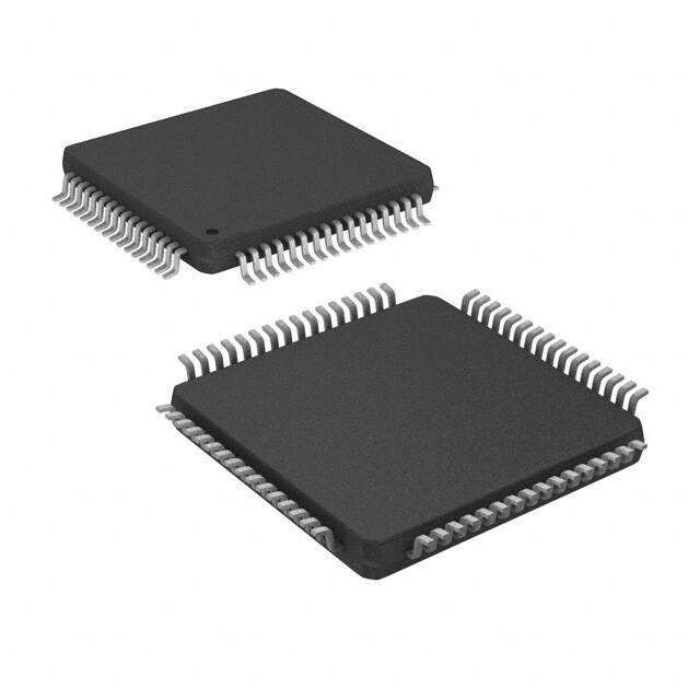


 工商网监
湘ICP备2023018690号
工商网监
湘ICP备2023018690号
