Analog Frequency Multiplier
PL560-XX VCXO Family
PRODUCT DESCRIPTION
The Analog Frequency Multiplier (AFM) is the
industry’s first ‘Balanced Oscillator’ utilizing analog
multiplication of the fundamental frequency (at
double or quadruple frequency), combined with an
attenuation of the fundamental of the reference
crystal, without the use of a phase-locked loop
(PLL), in CMOS technology.
Micrel’s world’s best performing AFM products can
achieve up to 800 MHz output frequency with little
jitter or phase noise deterioration. In addition, the
low frequency input crystal requirement makes the
AFMs the most affordable high-performance timingsource in the market.
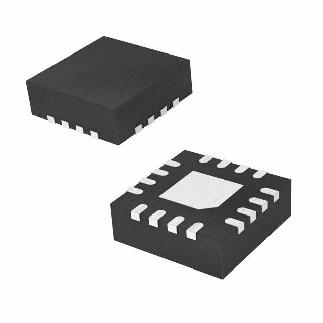
PL560/5-xx family of products utilize low-power
CMOS technology and are housed in Green / RoHS
compliant 16-pin TSSOP, and 16-pin 3x3 QFN
packages.
Non-PLL frequency multiplication
Input frequency from 30-200 MHz
Output frequency from 60-800 MHz
Low phase noise and jitter (equivalent to fundamental
crystal at the output frequency)
Ultra-low jitter
o RMS phase jitter < 0.25 ps (12kHz-20MHz)
o RMS period jitter < 2.5 ps
Low phase noise
o -142 dBc/Hz @100kHz offset from 155.52 MHz
o -150 dBc/Hz @10MHz offset from 155.52 MHz
High linearity pull range (typ. 5%)
+/- 120 PPM pullability VCXO
Low input frequency eliminates the need for expensive
crystals
Differential output levels (PECL, LVDS), or single ended CMOS
Single 3.3V, ±10% power supply
Optional industrial temperature range (-40C to +85C)
Available in 16-pin Green/RoHS compliant TSSOP, and
3x3 QFN packages
FEATURES
Figure 1: 2x AFM Phase Noise at 311.04MHz
Micrel Inc. • 2180 Fortune Drive • San Jose, CA 95131 • USA • tel +1(408) 944 -0800 • fax +1(408) 474-1000 • www.micrel.com Rev 11/04/11 Page 1
�Analog Frequency Multiplier
PL56X-XX VCXO Family
L2X
VCON
OE
XIN
Oscillator
Amplifier
XOUT
QBAR
Frequency
X2
Frequency
X4
Q
Only required in x4 designs
L4X
Figure 2: Block Diagram of VCXO AFM
Figure 3 shows the period jitter histogram of the 2x Analog Frequency Multiplier at 311.04 MHz, while F igure 4
shows the very low rejection levels of sub-harmonics that correspond to the exceptionally low jitter performance.
Figure 3: Period Jitter Histogram at 311.04 MHz
Analog Frequency Multiplier (2x)
with 155.52MHz crystal
Figure 4: Spectrum Analysis at 311.04 MHz
Analog Frequency Multiplier (2x)
with sub-harmonics below –72 dBc
OE LOGIC SELECTION
OUTPUT
OESEL
0 (Default)
LVPECL
1
0 (Default)
LVDS or LVCMOS
1
OE
Output State
0 (Default)
Enabled
1
Tri-state
0
Tri-state
1 (Default)
Enabled
0
Tri-state
1 (Default)
Enabled
0 (Default)
Enabled
1
Tri-state
OESEL and OE: Connect to VDD or leave floating to set to “1”, connect to GND to set to “0”.
Internally set to default through pull-down / -up.
Micrel Inc. • 2180 Fortune Drive • San Jose, CA 95131 • USA • tel +1(408) 944 -0800 • fax +1(408) 474-1000 • www.micrel.com Rev 11/04/11 Page 2
�Analog Frequency Multiplier
PL56X-XX VCXO Family
PRODUCT SELECTION GUIDE
FREQUENCY VERSUS PHASE NOISE PERFORMANCE
Phase Noise at Frequency Offset From Carrier (dBc/Hz)
Part
Number
Input
Frequency
Range
(MHz)
Analog
Frequency
Multiplication
Factor
Output
Frequency
Range
(MHz)
Output
Type
PL560-37
30 - 80
4
120 - 320
PL560-38
30 - 80
4
PL560-39
30 - 80
PL560-47
Carrier
Freq.
(MHz)
10Hz
100Hz
1kHz
10kHz
100kHz
1MHz
10MHz
LVCMOS
155.52
-50
-82
-110
-128
-142
-148
-150
120 - 320
LVPECL
155.52
-50
-82
-110
-128
-142
-148
-150
4
120 - 320
LVDS
155.52
-50
-82
-110
-128
-142
-148
-150
30 - 80
2
60 - 160
LVCMOS
155.52
-65
-95
-122
-138
-142
-148
-149
PL560-48
30 - 80
2
60 - 160
LVPECL
155.52
-65
-95
-122
-138
-142
-148
-149
PL560-49
30 - 80
2
60 - 160
LVDS
155.52
-65
-95
-122
-138
-142
-148
-149
PL560-68
75 - 200
2
150 - 400
LVPECL
311.04
-60
-85
-112
-135
-142
-150
-151
PL560-69
75 - 200
2
150 - 400
LVDS
311.04
-60
-85
-112
-135
-142
-150
-151
Phase noise was measured using Agilent E5500.
FREQUENCY VERSUS JITTER, AND SUB-HARMONIC PERFORMANCE
Part
Number
RMS
Period Jitter
(ps)
Peak to Peak
RMS
RMS Phase Jitter
Period Jitter Accumulated 12kHz to 20MHz Spectral Specifications / Sub-harmonic Content (dBc),
Output
(ps)
(L.T.) Jitter (ps)
(ps)
Frequency (MHz)
Freq.
Carrier
@
@
@
@
@
@
(MHz)
Min Typ Max Min Typ Max Min Typ Max Min Typ Max Freq. -75% -50% -25% +25% +50% +75%
(Fc)
(Fc)
(Fc)
(Fc)
(Fc)
(Fc)
(Fc)
PL560-37
155
2.5
3
18
20
3
0.25
155.52
-75
-62
-65
-75
PL560-38
155
2.5
3
18
20
3
0.25
155.52
-75
-62
-65
-75
PL560-39
155
2.5
3
18
20
3
0.25
155.52
-75
-62
-65
-75
PL560-47
155
2.5
3
18
20
3
0.25
155.52
-68
-68
PL560-48
155
2.5
3
18
20
3
0.25
155.52
-68
-68
PL560-49
155
2.5
3
18
20
3
0.27
155.52
-68
-68
PL560-68
311
2.5
3
18
20
3
0.18
311.04
-72
-85
PL560-69
311
2.5
3
18
20
3
0.18
311.04
-72
-85
Note: Wavecrest data 10,000 hits. No filtering was used in jitter calculations.
Agilent 5500 was used for phase jitter measurements.
Spectral specifications were obtained using Agilent E7401A.
Micrel Inc. • 2180 Fortune Drive • San Jose, CA 95131 • USA • tel +1(408) 944 -0800 • fax +1(408) 474-1000 • www.micrel.com Rev 11/04/11 Page 3
�Analog Frequency Multiplier
PL56X-XX VCXO Family
CRYSTAL SPECIFICATIONS AND BOARD LAYOUT CONSIDERATIONS
BOARD LAYOUT CONSIDERATIONS
AFM IC
AFM IC
XTAL
XIN (Pin # 4 )
XIN (Pin # 4 )
XTAL
XOUT (Pin # 5)
XOUT (Pin # 5)
Ceramic
SMD
To minimize parasitic effects, and improve performanc e:
Place the crystal as close as possible to the IC.
Make the board traces that are connected to the crystal pins symmetrical.
The board trace symmetry is important, as it reduces the negative parasitic effects to produce a clean
frequency multiplication with low jitter. Parasitic effects reduce frequency pulling of the VCXO and
increase jitter.
CRYSTAL SPECIFICATIONS & TUNING PERFORMANCE
CRYSTAL SPECIFICATIONS
PART
NUMBER
CRYSTAL
CL (xtal)
RESONATOR
MODE
FREQUENCY
CONDITYP
(FXIN)
TIONS
PL565-08
At
FundaPL560-09
75 to 200MHz
VCON =
mental
PL560-68/69
1.65V
PL56037/38/39
PL56047/48/49
TUNING PERFORMANCE
30 to 80MHz
At
FundaVCON =
mental
1.65V
5pF
5pF
ESR
(RE)
MAX
CRYSTAL
TUNING (Typical)
CRYSTAL
FREQ (MHz)
C0
C1
C0/C1
VC:
1.65V
0V
VC:
1.65V 3.3V
155.52
3.0pF
12.2fF
245
-145 ppm
+108 ppm
155.52
1.8pF
5.7fF
316
-134 ppm
+87 ppm
30.72
2.8pF
12.4fF
228
-167ppm
+176 ppm
30.72
4.5pF
19.1fF
236
-163 ppm
+167 ppm
38.88
5.1pF
20.9fF
242
-131 ppm
+98 ppm
38.88
5.3pF
25.6fF
207
-157 ppm
+141 ppm
77.76
2.0pF
6.7fF
305
-92 ppm
+110 ppm
30Ω
30Ω
Note: Non specified parameters can be chosen as standard values from crystal suppliers.
CL ratings larger than 5pF require a crystal frequency adjustment. Request detailed crystal specifications from Micrel.
Micrel Inc. • 2180 Fortune Drive • San Jose, CA 95131 • USA • tel +1(408) 944 -0800 • fax +1(408) 474-1000 • www.micrel.com Rev 11/04/11 Page 4
�Analog Frequency Multiplier
PL56X-XX VCXO Family
VOLTAGE CONTROL SPECIFICATION
PARAMETERS
VCXO Stabilization Time
SYMBOL
T VCXOSTB
CONDITIONS
MIN.
From power valid
VCXO Tuning Range
XTAL C0 /C 1
很抱歉,暂时无法提供与“PL560-48QC”相匹配的价格&库存,您可以联系我们找货
免费人工找货