(Prelim inary )
Analog Frequency Multiplier
PL560/565-08 VCXO Family
PRODUCT DESCRIPTION
FEATURES
The Analog Frequency Multiplier (AFM) is the
industry’s first ‘Balanced Oscillator’ utilizing analog
multiplication of the fundamental frequency (at
quadruple frequency), combined with an attenuation
of the fundamental of the reference crystal, without
the use of a phase-locked loop (PLL), in CMOS
technology.
Micrel’s world’s best performing AFM products can
achieve up to 800 MHz output frequency with little
jitter or phase noise deterioration. In addition, the
low frequency input crystal requirement makes the
AFM the most affordable high-performance timingsource in the market.
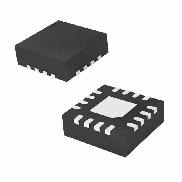
PL560-08 and PL565-08 products utilize low-power
CMOS technology and are housed in Green / RoHS
compliant 16-pin TSSOP, and 16-pin 3x3 QFN
packages.
12
14
VDDOSC
15
L2X
16
GNDBUF
Q
10
9
P560/5-08
1
2
3
4
8
VDDOSC
7
L4X
6
OE
5
XOUT
PL560-08 / PL565-08 BLOCK DIAGRAM
XIN
OESEL
11
VCON
13
OSCOFF
SEL
GNDOSC
VDDANA
QBAR
VDDBUF
QFN PACKAGE PIN-OUT
Non-PLL frequency multiplication by 4.
Input frequency from 62.5-200 MHz
Output frequency
o PL560-08: 250-600MHz
o PL565-08: 600-800MHz
Low phase noise and jitter (equivalent to fundamental
crystal at the output frequency)
Ultra-low jitter
o RMS phase jitter < 100 fs (12kHz-20MHz)
o RMS random period jitter < 2 ps
Low phase noise
o -142 dBc/Hz @100kHz offset from the carrier
o -150 dBc/Hz @10MHz offset from the carrier
High linearity pull range (typ. 5%)
VCXO, set pullability ±100ppm ~ ±200ppm
Low input frequency eliminates the need for expensive
crystals
Differential output levels: LVPECL
Single 3.3V, ±10% power supply
Optional industrial temperature range (-40C to +85C)
Available in 16-pin Green/RoHS compliant 3x3 QFN
packages and as die.
L2X
VCON
OE
XIN
Oscillator
Amplifier
XOUT
Frequency
X2
Frequency
X4
QBAR
Q
L4X
Micrel Inc. • 2180 Fortune Drive • San Jose, CA 95131 • USA • tel +1(408) 944 -0800 • fax +1(408) 474-1000 • www.micrel.com Rev 6/22/11 Page 1
�(Prelim inary )
Analog Frequency Multiplier
PL560/565-08 VCXO Family
DIE SPECIFICATIONS
16
17
15
14
Chip size, active area
13
12
19
11
20
1.385mm
Y
0,0
1
2
3
PAD size
80µm x 80µm
9
Scribe Line Dimension
X = 80µm
Y = 80µm
8
Chip Base
GND level
X
7
22
200 ± 20µm
10
Die ID
21
1.414mm x 1.385mm
Chip thickness
4
6
5
SCRIBE LINE
18
Die ID:
PL560-08DC
PL565-08DC
C561A 3222222
C561A 7777722
SCRIBE LINE
PAD/PIN ASSIGNMENT AND DESCRIPTION (The X/Y coordinates indicate pad centers)
Name
L4X
VDDOSC
GNDANA
GNDANA
GNDBUF
GNDBUF
GNDBUF
PECLB
PECL
VDDBUF
VDDBUF
VDDANA
N.C.
OESEL
VDDOSC
L2X
OSCOFFSEL
GNDOSC
VCON
XIN
XOUT
OE
Pad Assignment*
Pad # X (µm) Y (µm)
1
2
3
4
5
6
7
8
9
10
11
12
13
14
15
16
17
18
19
20
21
22
-352
-183
+15
+144
+292
+469
+502
+502
+502
+502
+571
+571
+377
+183
-57
-214
-410
-572
-572
-572
-572
-572
-557
-557
-557
-557
-557
-557
-365
-215
-54
+79
+236
+413
+554
+554
+554
+554
+554
+554
+394
+199
-309
-521
QFN
Pin #
Type
7
8
9
10
11
12
13
14
15
16
1
2
3
4
5
6
Description
I
P
P
P
P
P
P
O
O
P
P
P
External inductor connection
VDD connection
GND connection
GND connection
GND connection
GND connection
GND connection
LVPECL complementary output
LVPECL output
VDD connection
VDD connection
VDD connection
I
P
I
I
P
I
I
O
I
OE style selection pin
VDD connection
External inductor connection
Oscillator Off selection pin
GND connection
Control voltage input
Crystal Input pad
Crystal Output pad
Output Enable input
* Note: Pad coordinates referenced to the center of the die.
Micrel Inc. • 2180 Fortune Drive • San Jose, CA 95131 • USA • tel +1(408) 944 -0800 • fax +1(408) 474-1000 • www.micrel.com Rev 6/22/11 Page 2
�(Prelim inary )
Analog Frequency Multiplier
PL560/565-08 VCXO Family
AFM Phase Noise at 491.52MHz, using 122.88MHz crystal
AFM Spectrum at 491.52MHz, using 122.88MHz crystal
The analog frequency multiplication preserves the low phase noise of the quartz crystal oscillator while keeping
unwanted sub harmonics from the multiplication at very low levels. Sub harmonics appear only at large distance
from the carrier, far outside the loop bandwidth of a PLL that uses the AFM signal to multiply up further to a
multiple GHz network clock. This means the impact of the sub harmonics on the application is negligible.
Micrel Inc. • 2180 Fortune Drive • San Jose, CA 95131 • USA • tel +1(408) 944 -0800 • fax +1(408) 474-1000 • www.micrel.com Rev 6/22/11 Page 3
�(Prelim inary )
Analog Frequency Multiplier
PL560/565-08 VCXO Family
PHASE NOISE PERFORMANCE
Part
Number
Input
Freq.
Range
(MHz)
Output
Freq.
Range
(MHz)
PL560-08
62.5 - 150
250 - 600
10
Hz
100
Hz
1
kHz
10
kHz
100
kHz
1
MHz
10
MHz
Phase
Jitter
12KHz ~
20MHz
(ps)
-64
-96
-123
-135
-141
-150
-155
0.05
-56
-87
-113
-134
-143
-149
-153
0.04
Phase Noise at Frequency Offset From Carrier (dBc/Hz)
Carrier
Freq.
(MHz)
491.52
PL565-08
150 - 200
600 - 800
622.08
Phase noise was measured using Agilent E5052B.
SUB-HARMONIC PERFORMANCE
Part
Number
Input
Output
Frequency Frequency
(MHz)
(MHz)
Spectral Specifications / Sub-harmonic Content (dBc), Freq. (MHz)
Carrier
Freq.
(Fc)
@
-75%
(Fc)
@
-50%
(Fc)
@
-25%
(Fc)
@
+25%
(Fc)
@
+50%
(Fc)
@
+75%
(Fc)
PL560-08
122.88
491.52
491.52
-60
-40
-70
-70
-40
-70
PL565-08
155.52
622.08
622.08
-60
-40
-40
-40
-40
-50
Note: Spectral specifications were obtained using Agilent E7401A
AFM MULTIPLYING TECHNIQUE
The analog frequency multiplication is achieved through a “squaring” operation.
The math is as follows: SIN²(x) = 0.5 - 0.5×COS(2x)
A very important property of this processing is that the result is a pure sine wave with double frequency. In theory
there are no sub harmonics but in practice the squaring operation is not perfect and a low level of sub harmonics
is present anyway. The key is that the resulting sub harmonics are very low and simple filtering with o nly one
inductor per squarer is adequate for excellent performance.
Micrel Inc. • 2180 Fortune Drive • San Jose, CA 95131 • USA • tel +1(408) 944 -0800 • fax +1(408) 474-1000 • www.micrel.com Rev 6/22/11 Page 4
�(Prelim inary )
Analog Frequency Multiplier
PL560/565-08 VCXO Family
AFM DIE APPLICATION CIRCUIT
A 7x5mm ceramic substrate was designed to assemble and operate the AFM die at optimum performance:
VDD
VCON
PECLB
PECL
OE
GND
Substrate part number: Kyocera KD-VB0F48
Please see PL560-08DC and PL565-08DC Tuning Assistant documents for passive component values.
Micrel Inc. • 2180 Fortune Drive • San Jose, CA 95131 • USA • tel +1(408) 944 -0800 • fax +1(408) 474-1000 • www.micrel.com Rev 6/22/11 Page 5
�(Prelim inary )
Analog Frequency Multiplier
PL560/565-08 VCXO Family
AFM QFN PACKAGE APPLICATION CIRCUIT
RECOMMENDED PCB LAYOUT
Avoid ground planes underneath the crystal
and inductor traces to limit parasitic
capacitance.
Add bypass capacitor close to VDDBUF pin.
Avoid bypass capacitors near VDDOSC pins to
lower cross-talk of unwanted frequencies.
L1X(a,b) can be used to increase the VCXO
pulling range. Using a ferrite core inductor
limits the oscillation amplitude which can have
a positive effect on phase noise.
L2X and L4X tune the frequency multiplier tank
circuits. They need to be wire wound inductors
with high Q-factor, preferably >20.
The large center pad is the “thermal relief” pad
and can be connected to ground.
Micrel Inc. • 2180 Fortune Drive • San Jose, CA 95131 • USA • tel +1(408) 944 -0800 • fax +1(408) 474-1000 • www.micrel.com Rev 6/22/11 Page 6
�(Prelim inary )
Analog Frequency Multiplier
PL560/565-08 VCXO Family
INDUCTOR VALUE OPTIMIZATION
The required inductor values for the best performance depend on the operating frequency, and the board layout
or module specifications. The listed values in this datasheet are based on the calculated parasitic values fr om
Micrel’s evaluation board design. These inductor values provide the user with a starting point to determine the
optimum inductor values. Additional fine -tuning may be required to determine the optimal solution.
The inductor is recommended to be a hi gh Q small size 0402 or 0603 SMD component, and must be placed
between L2X / L4X and adjacent VDDOSC pin. Place inductor as close to the IC as possible to minimize parasitic
effects and to maintain inductor Q.
To assist with the inductor value optimization, Micrel has developed AFM “Tuning Assistant” documents. You can
download these documents from Micrel’s web site (www.micrel.com). The documents consist of tables with
recommended inductor values for certain output frequency ranges.
Figure 10: Diagram Representation of the Related System Inductance and Capacitance
DIE SIDE
- Cinternal at L2X = 7.625 pF , at L4X = 6.25 pF
- Cpad = 1.0 pF, Bond pad and its ESD circuitry
- C11 = 0.4 pF, The following amplifier stage
PCB side
- LWB1 = 2 nH, (2 places), Stray inductance
- Cstray = 0.5 pF, Stray capacitance
- L2X (L4X) = 2x or 4x inductor
- C2X (C4X) = range (0.1 to 2.7 pF), Fine tune
the tank, if used.
Work out the resonance of this network and you have a good first guess for the require d inductor values for
optimum performance. Non-linear behavior at large signal amplitudes can shift the tank resonance significantly,
especially at the L2X side, to a lower frequency than the calculation suggests. The Tuning Assistant documents
are based upon actual lab tests and are corrected for the non -linear behavior.
Micrel Inc. • 2180 Fortune Drive • San Jose, CA 95131 • USA • tel +1(408) 944 -0800 • fax +1(408) 474-1000 • www.micrel.com Rev 6/22/11 Page 7
�(Prelim inary )
Analog Frequency Multiplier
PL560/565-08 VCXO Family
ELECTRICAL SPECIFICATIONS
ABSOLUTE MAXIMUM RATINGS
PARAMETERS
SYMBOL
Supply Voltage
MIN.
V DD
MAX.
UNITS
4.6
V
Input Voltage, DC
VI
GND-0.5
V DD+0.5
V
Output Voltage, DC
VO
GND-0.5
V DD+0.5
V
Storage Temperature
TS
-65
150
C
Ambient Operating Temperature, Industrial
T A_ I
-40
+85
C
Ambient Operating Temperature, Commercial
T A_ C
0
+70
C
125
C
260
C
2
kV
Junction Temperature
TJ
Lead Temperature (soldering, 10s)
Input Static Discharge Voltage Protection (HBM)
Exposure of the device under conditions beyond the limits specified by Maximum Ratings for extended periods may cause permane nt damage to the
device and affect product reliability. These conditions represent a stress rating only, and functional operations of the device at these or any other
conditions above the operational limits noted in this specification is not implied .
VOLTAGE CONTROL SPECIFICATION
PARAMETERS
VCXO Stabilization Time
SYMBOL
T VCXOSTB
CONDITIONS
MIN.
From power valid
VCXO Tuning Range*
XTAL C0 /C 1
很抱歉,暂时无法提供与“PL565-08QC-R”相匹配的价格&库存,您可以联系我们找货
免费人工找货