PL60708X
PCIe Octal, Ultra-Low Jitter,
HCSL Frequency Synthesizer
General Description
Features
The PL607081 and PL607082 are members of the PCI
Express family of devices from Micrel and provide
extremely low-noise spread-spectrum clocks for PCI
Express requirements.
Generates eight HCSL clock outputs
PL607081 output frequencies: 25MHz, 100MHz, or
200MHz
PL607082 output frequencies: 25MHz, 125MHz, or
250MHz
Spread spectrum for EMI reduction
2.5V or 3.3V operating range
Typical phase jitter @ 100MHz: 320fs for 1.5MHz to
10MHz
Compliant with PCI Express Gen1, Gen2, and Gen3
Industrial temperature range (–40°C to +85°C)
RoHS and PFOS compliant
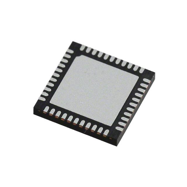
Available in a 44-pin 7mm × 7mm QFN package
The devices operate from a 3.3V or 2.5V power supply
and synthesize eight HCSL output clocks. The PL607081
synthesizes 25MHz, 100MHz, or 200MHz frequencies and
the PL607082 synthesizes 25MHz, 125MHz, or 250MHz
frequencies. The PL60708x devices accept a 25MHz
crystal or LVCMOS reference clock.
Datasheets and support documentation are available on
Micrel’s web site at: www.micrel.com.
Block Diagram
Applications
Servers
Storage systems
Switches and routers
Gigabit Ethernet
Set-top boxes/DVRs
Ripple Blocker is a trademark of Micrel, Inc.
Micrel Inc. • 2180 Fortune Drive • San Jose, CA 95131 • USA • tel +1 (408) 944-0800 • fax + 1 (408) 474-1000 • http://www.micrel.com
April 1, 2014
Revision 1.2
tcghelp@micrel.com or (408) 955-1690
�Micrel, Inc.
PL60708X
Ordering Information(1)
Part Number
Marking
Shipping
Junction Temperature Range
Package
PL607081UMG
PL607
081
Tray
–40°C to +85°C
44-Pin QFN
PL607081UMG TR
PL607
081
Tape and Reel
–40°C to +85°C
44-Pin QFN
PL607082UMG
PL607
082
Tray
–40°C to +85°C
44-Pin QFN
PL607082UMG TR
PL607
082
Tape and Reel
–40°C to +85°C
44-Pin QFN
Note:
1. Devices are RoHS and PFOS compliant.
April 1, 2014
2
Revision 1.2
tcghelp@micrel.com or (408) 955-1690
�Micrel, Inc.
PL60708X
Pin Configuration
44-Pin QFN
(Top View)
Pin Description
Pin Number
Pin Name
Pin Type
Pin Level
1, 2
4, 5
7, 8
25, 26
29, 30
32, 33
36, 37
41, 42
/Q5, Q5
/Q6, Q6
/Q7, Q7
/Q0, Q0
/Q1, Q1
/Q2, Q2
/Q3, Q3
/Q4, Q4
O, (DIF)
HCSL
14
FSEL
I, (SE)
LVCMOS
12, 13, 34
VDD
PWR
Power supply
31
VDDO1
PWR
Power supply for outputs Q0–Q3
43
VDDO2
PWR
Power supply for outputs Q4–Q7
16, 19, 20, 21,
44
VSS
(exposed
pad)
PWR
Core power supply ground. The exposed pad must be
connected to the VSS ground plane.
24
VSSO1
PWR
Power supply ground for outputs Q0–Q3
39
VSSO2
PWR
Power supply ground for outputs Q4–Q7
10
GND
I
April 1, 2014
Pin Name
Differential clock output
LVCMOS
3
Frequency select, 45kΩ pull-up
PL607081: 1 = 100MHz, 0 = 200MHz
PL607082: 1 = 125MHz, 0 = 250MHz
This pin is not a power supply ground but must be tied to
VSS for proper operation.
Revision 1.2
tcghelp@micrel.com or (408) 955-1690
�Micrel, Inc.
PL60708X
Pin Description (Continued)
Pin Number
Pin Name
Pin Type
Pin Name
LVCMOS
PLL bypass, selects output source.
0 = normal PLL operation
1 = output from input reference clock or crystal
45kΩ pull-down
9
PLL_BYPASS
3, 11, 17, 18,
23, 27, 35
TEST
40
XIN/FIN
I, (SE)
15pF crystal
Crystal or reference clock input, no load caps needed (see
Figure 7)
38
XOUT
O, (SE)
15pF crystal
Crystal output, no load caps needed (see Figure 7)
15
OE1
I, (SE)
LVCMOS
Output enable, outputs Q0–Q3 disable to tri-state,
0 = Disabled, 1 = Enabled, 45kΩ pull-up
22
OE2
I, (SE)
LVCMOS
Output enable, outputs Q4–Q7 disable to tri-state,
0 = Disabled, 1 = Enabled, 45kΩ pull-up
28
SS0
I, (SE)
LVCMOS
Spread-spectrum select, 60kΩ pull-up
0 = Spread OFF, 1 = Spread ON
6
SS1
I, (SE)
LVCMOS
April 1, 2014
I, (SE)
Pin Level
Factory test pins. Do not connect anything to these pins.
4
Spread-spectrum select, 60kΩ pull-up
0 = 0.25%, 1 = Spread 0.50%
Revision 1.2
tcghelp@micrel.com or (408) 955-1690
�Micrel, Inc.
PL60708X
EMI Reduction
Spread-spectrum modulation reduces the emission of
spectral components in the clock signal. The spectrum plot
on the right (Figure 1) shows measurement results with the
two spread settings versus no spread. This plot refers to
the 11th harmonic in a 100MHz clock, at 1.1GHz. The
scale is normalized to the strength of this spur without
spread. The plot shows about 21dB reduction for 0.25%
spread magnitude and 24dB for 0.50% spread magnitude.
The plot also shows
downwards.
how the frequency spreads
Figure 1. Spectrum Plot
April 1, 2014
5
Revision 1.2
tcghelp@micrel.com or (408) 955-1690
�Micrel, Inc.
PL60708X
Absolute Maximum Ratings(2)
Operating Ratings(3)
Supply Voltage (VDD, VDDO1/2) ...................................... +4.6V
Input Voltage (VIN) ............................... 0.50V to VDD +0.5V
Lead Temperature (soldering, 20s) ............................ 260°C
Case Temperature ..................................................... 115°C
Storage Temperature (TS) ......................... 65°C to +150°C
Supply Voltage (VDD, VDDO1/2) ............... +2.375V to +3.465V
Ambient Temperature (TA) .......................... –40°C to +85°C
(4)
Junction Thermal Resistance
QFN (JA) Still-Air ............................................... 24°C/W
QFN (JB) Junction-to-Board ............................... 8°C/W
DC Electrical Characteristics(5)
VDD = VDDO1/2 = 3.3V ±5% or 2.5V ±5%
VDD = 3.3V ±5%, VDDO1/2 = 3.3V ±5% or 2.5V ±5%
TA = 40°C to +85°C
Symbol
Parameter
VDD,
VDDO1/2
VDD,
VDDO1/2
IDD
Min.
Typ.
Max.
Units
2.5V Operating Range
2.375
2.5
2.625
V
3.3V Operating Range
3.135
3.3
3.465
V
Eight outputs enabled, 100MHz
Outputs 50Ω to VSS
230
285
Eight outputs enabled, 200MHz
Outputs 50Ω to VSS
240
300
Four outputs enabled, 100MHz
Outputs 50Ω to VSS, OE1 or OE2 = 0
160
200
Four outputs enabled, 200MHz
Outputs 50Ω to VSS, OE1 or OE2 = 0
170
210
Min.
Typ.
Max.
Units
Supply Current VDD + VDDO
Condition
mA
HCSL DC Electrical Characteristics(5)
VDD = VDDO1/2 = 3.3V ±5% or 2.5V ±5%
VDD = 3.3V ±5%, VDDO1/2 = 3.3V ±5% or 2.5V ±5%
TA = 40°C to +85°C. RL = 50Ω to VSS
Symbol
Parameter
Condition
VOH
Output High Voltage
660
700
850
mV
VOL
Output Low Voltage
150
0
27
mV
VCROSS
Crossing Point Voltage
250
350
550
mV
Notes:
2. Exceeding the absolute maximum ratings may damage the device.
3. The device is not guaranteed to function outside its operating ratings.
4. Package thermal resistance assumes that the exposed pad is soldered (or equivalent) to the device’s most negative potential on the PCB.
5. Specification for packaged product only.
April 1, 2014
6
Revision 1.2
tcghelp@micrel.com or (408) 955-1690
�Micrel, Inc.
PL60708X
LVCMOS (PLL_BYPASS, FSEL, OE1, OE2, SS0, SS1) DC Electrical Characteristics(5)
VDD = 3.3V ±5% or 2.5V ±5%, TA = 40°C to +85°C.
Symbol
Parameter
Condition
Min.
VIH
Input High Voltage
VIL
Input Low Voltage
IIH
Input High Current
VDD = VIN = 3.465V
IIL
Input Low Current
VDD = 3.465V, VIN = 0V
150
Parameter
Condition
Min.
Mode of Oscillation
15pF load
Typ.
Max.
Units
2
VDD + 0.3
V
0.3
0.8
V
150
µA
µA
Crystal Characteristics
Typ.
Max.
Units
Fundamental, parallel resonant
Frequency
25
Equivalent Series Resistance (ESR)
MHz
50
Ω
Shunt Capacitor, C0
2
5
pF
Correlation Drive Level
10
100
µW
April 1, 2014
7
Revision 1.2
tcghelp@micrel.com or (408) 955-1690
�Micrel, Inc.
PL60708X
AC Electrical Characteristics(4, 6)
VDD = VDDO1/2 = 3.3V ±5% or 2.5V ±5%
VDD = 3.3V ±5%, VDDO1/2 = 3.3V ±5% or 2.5V ±5%
TA = 40°C to +85°C. RL = 50Ω to VSS
Symbol
FOUT
Parameter
Condition
Min.
Typ.
Max.
Units
PL607081
25
100
200
MHz
PL607082
25
125
250
MHz
Output Frequency
FREF
Crystal Input Frequency
25
MHz
FIN
Reference Input Frequency
25
MHz
FIN
FIN Signal Amplitude
Internally AC Coupled
0.9
TR/TF
HCSL Output Rise/Fall Time
20%80%
150
ODC
Output Duty Cycle
48
TSKEW
Output-to-Output Skew
TLOCK
PLL Lock Time
(8)
RMS Phase Jitter
Tjit()
VDD
Vpp
300
450
ps
50
52
%
45
ps
20
ms
Note 7
100MHz
Integration Range (1.5MHz to 10MHz)
320
Cycle to Cycle Jitter
fs
30
ps,
peak
Spread Spectrum Characteristics
Parameter
Modulation Rate
Condition
Min.
(9)
Modulation Magnitude
Typ.
Max.
31.6
(10)
Units
kHz
Setting is 0.25%
-0.073 to -0.265
0 to 0.250
+0.031 to -0.375
%
Setting is 0.50%
-0.136 to -0.383
0 to 0.500
+0.078 to -0.589
%
Notes:
6. All phase noise measurements were taken with an Agilent 5052B phase noise system.
7. Defined as skew between outputs at the same supply voltage and with equal load conditions; measured at the output differential crossing points.
8. Measured using a 25MHz crystal as the input reference source. If using an external reference input, use a low phase noise source. With an external
reference, the phase noise follows the input source phase noise up to about 1MHz.
9. The modulation rate is the crystal frequency divided by 792.
10. The typical modulation makes the output frequency sweep between the target frequency (0%) and the down-spread value (0.25% or 0.5%). There
is process variation on the modulation magnitude; the smallest and largest possible modulation magnitude sweep ranges are listed in the Spread
Spectrum Characteristics table.
April 1, 2014
8
Revision 1.2
tcghelp@micrel.com or (408) 955-1690
�Micrel, Inc.
PL60708X
Truth Tables
OE2
OE1
OUTPUT
0
1
Q4-Q7 Tri-state
1
0
Q0-Q3 Tri-state
FSEL
PLL_BYPASS
0
Output Frequency (MHz)
PL607081
PL607082
0
200
250
1
0
100
125
X
1
25
25
Spread Type
Spread
SS1
(11)
SS0
(11)
0
0
Spread is OFF
No Spread
0
1
Down Spread
0.25%
1
0
Spread is OFF
No Spread
1
1
Down Spread
0.50%
Note:
11. SS0 turns ON/OFF spread-spectrum modulation and SS1 selects the spread magnitude.
April 1, 2014
9
Revision 1.2
tcghelp@micrel.com or (408) 955-1690
�Micrel, Inc.
PL60708X
Phase Noise Plot
Phase Noise Plot: 100MHz, 1.5MHz to 10MHz 320fs
April 1, 2014
10
Revision 1.2
tcghelp@micrel.com or (408) 955-1690
�Micrel, Inc.
PL60708X
Figure 2. Duty Cycle Timing
Figure 3. All Outputs Rise/Fall Time
Figure 4. RMS Phase/Noise Jitter
Figure 5. HCSL Output Load and Test Circuit
April 1, 2014
11
Revision 1.2
tcghelp@micrel.com or (408) 955-1690
�Micrel, Inc.
PL60708X
Figure 6. HCSL Recommended Application Termination (source terminated)
Figure 7. Crystal Input Interface
April 1, 2014
12
Revision 1.2
tcghelp@micrel.com or (408) 955-1690
�Micrel, Inc.
PL60708X
Application Information
The impedance value of the ferrite bead (FB) must be
between 240Ω and 600Ω with a saturation current
≥150mA.
Crystal Layout
Keep the layers under the crystal as open as possible
and do not place switching signals or noisy supplies
under the crystal. Crystal load capacitance is built inside
the die so no external capacitance is needed. See the
Selecting a Quartz Crystal for the Clockworks Flex Family
of Precision Synthesizers application note for more
details.
The VDDO1 and VDDO2 pins connect directly to the
VDD plane. All VDD pins on the PL60708X connect to
VDD after the power supply filter.
HCSL Outputs
Terminate HCSL outputs with 50Ω to VSS. For best
performance, load all outputs. If you want to AC-couple or
change the termination, contact Micrel’s applications
group at: tcghelp@micrel.com (see Figure 6).
Contact
Micrel’s HBW
applications group
at:
tcghelp@micrel.com if you need help selecting a suitable
crystal for your application
Power Supply Decoupling
Place the smallest value decoupling capacitor (4.7nF)
between the VDD and VSS pins, as close as possible to
those pins and at the same side of the PCB as the IC.
The shorter the physical path from VDD to capacitor and
back from capacitor to VSS, the more effective the
decoupling. Use one 4.7nF capacitor for each VDD pin
on the PL60708X.
Power Supply Filtering Recommendations
Preferred filter, using Micrel MIC94300 or MIC94310 Ripple Blocker™:
Alternative, traditional filter, using a ferrite bead:
April 1, 2014
13
Revision 1.2
tcghelp@micrel.com or (408) 955-1690
�Micrel, Inc.
PL60708X
Package Information(12)
44-Pin QFN
Note:
12. Package information is correct as of the publication date. For updates and most current information, go to www.micrel.com.
MICREL, INC. 2180 FORTUNE DRIVE SAN JOSE, CA 95131 USA
TEL +1 (408) 944-0800 FAX +1 (408) 474-1000 WEB http://www.micrel.com
Micrel makes no representations or warranties with respect to the accuracy or completeness of the information furnished in this data sheet. This
information is not intended as a warranty and Micrel does not assume responsibility for its use. Micrel reserves the right to change circuitry,
specifications and descriptions at any time without notice. No license, whether express, implied, arising by estoppel or otherwise, to any intellectual
property rights is granted by this document. Except as provided in Micrel’s terms and conditions of sale for such products, Micrel assumes no liability
whatsoever, and Micrel disclaims any express or implied warranty relating to the sale and/or use of Micrel products including liability or warranties
relating to fitness for a particular purpose, merchantability, or infringement of any patent, copyright or other intellectual property right.
Micrel Products are not designed or authorized for use as components in life support appliances, devices or systems where malfunction of a product
can reasonably be expected to result in personal injury. Life support devices or systems are devices or systems that (a) are intended for surgical
implant into the body or (b) support or sustain life, and whose failure to perform can be reasonably expected to result in a significant injury to the user. A
Purchaser’s use or sale of Micrel Products for use in life support appliances, devices or systems is a Purchaser’s own risk and Purchaser agrees to fully
indemnify Micrel for any damages resulting from such use or sale.
© 2014 Micrel, Incorporated.
April 1, 2014
14
Revision 1.2
tcghelp@micrel.com or (408) 955-1690
�