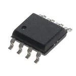
QT118HA-ISG
lQ
NOT RECOMMENDED FOR NEW DESIGNS
Less expensive than many mechanical switches
Projects a ‘touch button’ through any dielectric
100% autocal for life - no adjustments required
No active external components
Piezo sounder direct drive for ‘tactile’ click feedback
LED drive for visual feedback
2 ~ 5V single supply operation
10µ
µA at 2.5V - very low power drain
Toggle mode for on/off control (via option pins)
10s or 60s auto-recalibration timeout (via option pins)
Pulse output mode (via option pins)
Gain settings in 3 discrete levels
Simple 2-wire operation possible
HeartBeat™ health indicator on output
Pb-Free package
Vdd
1
Out
2
Opt1
3
Opt2
4
QT118HA
�
�
�
�
�
�
�
�
�
�
�
�
�
�
�
8
Vss
7
Sns2
6
Sns1
5
Gain
The QT118HA is a Flash version of the QT118H. The QT118HA is form, fit and function
compatible with the older device, except that the QT118HA is more sensitive than the
older device, necessitating a significant reduction in Cs capacitance. See Section 1 on page 2 for
differences.
This device is intended as a replacement for the QT118H in existing
designs already in production, but is not recommended for new designs.
For further device migration plans please
consult your local Atmel or Quantum representative.
lq
©1999-2008 Quantum Research Group
QT118HA_AR1.02_0408
�Figure 1-1 Standard mode options
1 - OVERVIEW
The QT118HA is intended to replace the QT118H as a lower
cost alternative. This device functions identically to the QT118H,
except that it is more sensitive. To compensate for the sensitivity
increase, it is required to do either of these two things:
+2 ~~+5
+2.5
+5
1. Increase the Cx loading to ground on SNS2 by 10pF
2. Decrease the Cs value
1
2
Option 1 is very simple and guarantees that the sensitivity of the
QT118HA is identical to the older device. Option 2 requires
some trial and error to test the sensitivity of the touch pad or
prox field, so that it is about the same as before. Cs changes
ranging from 10 - 60% may be required depending on the circuit
layout and electrode design.
3
Vdd
OUT
SNS2
OPT1
GAIN
RE
7
5
Rs
Cs
4
OUTPUT = DC
TIMEOUT = 10 Secs
TOGGLE = OFF
GAIN = HIGH
All other aspects of this datasheet are identical to the QT118H
datasheet except for this section and specifications on pages 9
and 10, and the part marking.
1.1 BASIC OPERATION
The QT118HA employs short, low duty cycle bursts of QT cycles
to acquire capacitance. Burst mode permits power consumption
in the low microamp range, dramatically reduces RF emissions,
lowers susceptibility to EMI, and yet permits excellent response
time. Internally the signals are digitally processed to reject
impulse noise, using a 'consensus' filter which requires four
consecutive confirmations of a detection before the output is
activated.
OPT2
SNS1
SENSING
ELECTRODE
Cx
6
2nF - 500nF
Vss
8
Option pins allow the selection or alteration of several special
features and sensitivity.
1.2 ELECTRODE DRIVE
The internal ADC treats Cs as a floating transfer capacitor; as a
direct result, the sense electrode can in theory be connected to
either SNS1 or SNS2 with no performance difference. However,
the noise immunity of the device is improved by connecting the
electrode to SNS2, preferably via a series resistor Re (Figure
1-1) to roll off higher harmonic frequencies, both outbound and
inbound.
The QT switches and charge measurement hardware functions
are all internal to the QT118HA (Figure 1-3). A single-slope
switched capacitor ADC includes both the required QT charge
and transfer switches in a configuration that provides direct ADC
conversion. The sensitivity depends on the values of Cs, Cx,
and to a smaller degree, Vdd. Vdd is used as the charge
reference voltage.
In order to reduce power consumption and to assist in
discharging Cs between acquisition bursts, a 470K series
resistor Rs should always be connected across Cs (Figure 1-1).
The rule Cs >> Cx must be observed for proper operation.
Normally Cx is on the order of 10pF or so, while Cs might be
10nF (10,000pF), or a ratio of about 1:1000.
Higher values of Cs increase gain; higher values of Cx load
reduce it. The value of Cs can thus be increased to allow larger
values of Cx to be tolerated (Figures 4-1 and 4-2, page 10).
It is important to minimize the amount of unnecessary stray
capacitance Cx, for example by minimizing trace lengths and
widths and backing off adjacent ground traces and planes so as
keep gain high for a given value of Cs, and to allow for a larger
sensing electrode size if so desired.
Piezo sounder drive: The QT118HA can drive a piezo sounder
after a detection for feedback. The piezo sounder replaces or
augments the Cs capacitor; this works since piezo sounders are
also capacitors, albeit with a large thermal drift coefficient. If
Cpiezo is in the proper range, no additional capacitor. If Cpiezo is
too small, it can simply be ‘topped up’ with a ceramic capacitor
in parallel. The QT118HA drives a ~4kHz signal across SNS1
and SNS2 to make the piezo (if installed) sound a short tone for
75ms immediately after detection, to act as an audible
confirmation.
The PCB traces, wiring, and any components associated with or
in contact with SNS1 and SNS2 will become touch sensitive and
should be treated with caution to limit the touch area to the
desired location.
Figure 1-2 2-wire operation, self-powered
+
3.5 - 5.5V
CMOS
LOGIC
1K
Twisted
pair
10µF
1
1N4148
2
Vdd
OUT
SNS2
n-ch Mosfet
3
4
OPT1
GAIN
OPT2
SNS1
RE
7
5
SENSING
ELECTRODE
Cs
Rs
Cx
6
Vss
8
lq
2
QT118HA_AR1.02_0408
�1.3 ELECTRODE DESIGN
Figure 1-3 Internal Switching & Timing
1.3.1 ELECTRODE GEOMETRY AND SIZE
E LEC TRO DE
Result
Single -Slo pe 14-bit
Switched Cap acito r AD C
Start
S NS2
Bu rst C ontroller
There is no restriction on the shape of
the electrode; in most cases common
sense and a little experimentation can
result in a good electrode design. The
QT118HA will operate equally well with
long, thin electrodes as with round or
square ones; even random shapes are
acceptable. The electrode can also be
a 3-dimensional surface or object.
Sensitivity is related to electrode
surface area, orientation with respect
to the object being sensed, object
composition, and the ground coupling
quality of both the sensor circuit and
the sensed object.
Do ne
Cs
Cx
S NS1
C harg e
Amp
1.3.2 KIRCHOFF’S CURRENT LAW
Like all capacitance sensors, the
QT118HA relies on Kirchoff’s Current
Law (Figure 1-5) to detect the change
in capacitance of the electrode. This law as applied to
capacitive sensing requires that the sensor’s field current
must complete a loop, returning back to its source in order for
capacitance to be sensed. Although most designers relate to
Kirchoff’s law with regard to hardwired circuits, it applies
equally to capacitive field flows. By implication it requires that
the signal ground and the target object must both be coupled
together in some manner for a capacitive sensor to operate
properly. Note that there is no need to provide actual
hardwired ground connections; capacitive coupling to ground
(Cx1) is always sufficient, even if the coupling might seem
very tenuous. For example, powering the sensor via an
isolated transformer will provide ample ground coupling,
since there is capacitance between the windings and/or the
transformer core, and from the power wiring itself directly to
'local earth'. Even when battery powered, just the physical
size of the PCB and the object into which the electronics is
embedded will generally be enough to couple a few
picofarads back to local earth.
1.3.3 VIRTUAL CAPACITIVE GROUNDS
When detecting human contact (e.g. a fingertip), grounding
of the person is never required. The human body naturally
has several hundred picofarads of ‘free space’ capacitance to
the local environment (Cx3 in Figure 1-4), which is more than
two orders of magnitude greater than that required to create
a return path to the QT118HA via earth. The QT118HA's PCB
however can be physically quite small, so there may be little
‘free space’ coupling (Cx1 in Figure 1-4) between it and the
environment to complete the return path. If the QT118HA
circuit ground cannot be earth grounded by wire, for example
via the supply connections, then a ‘virtual capacitive ground’
may be required to increase return coupling.
crumpled into a ball. Virtual ground planes are more effective
and can be made smaller if they are physically bonded to
other surfaces, for example a wall or floor.
‘Ground’ as applied to capacitive fields can also mean power
wiring or signal lines. The capacitive sensor, being an AC
device, needs only an AC ground return.
1.3.5 SENSITIVITY ADJUSTMENT
1.3.5.1 Gain Pin
The QT118HA can be set for one of 3 gain levels using
option pin 5 (Table 1-1). This sensitivity change is made by
altering the internal numerical threshold level required for a
detection. Note that sensitivity is also a function of other
things: like the values of Cs and Cx, electrode size, shape,
and orientation, the composition and aspect of the object to
be sensed, the thickness and composition of any overlaying
panel material, and the degree of ground coupling of both
sensor and object.
The Gain input should never be connected to a pullup or
pulldown resistor or tied to anything other than SNS1 or
SNS2, or left unconnected (for high gain setting).
Figure 1-4 Kirchoff's Current Law
CX2
Se nse E le ctro de
A ‘virtual capacitive ground’ can be created by connecting the
QT118HA’s own circuit ground to:
SENSO R
- A nearby piece of metal or metallized housing;
- A floating conductive ground plane;
- Another electronic device (to which its might be
connected already).
CX1
Free-floating ground planes such as metal foils should
maximize exposed surface area in a flat plane if possible. A
square of metal foil will have little effect if it is rolled up or
lq
Su rro und ing e nv iro nm en t
3
C X3
QT118HA_AR1.02_0408
�Drift compensation (Figure 2-1) is performed by making the
reference level track the raw signal at a slow rate, but only
while there is no detection in effect. The rate of adjustment
must be performed slowly, otherwise legitimate detections
could be ignored. The QT118HA drift compensates using a
slew-rate limited change to the reference level; the threshold
and hysteresis values are slaved to this reference.
Table 1-1 Gain Strap Options
Gain
High
Medium
Low
Tie Pin 5 to:
Leave open
Pin 6
Pin 7
1.3.5.2 Changing Cs, Cx
The values of Cs and Cx have a dramatic effect on
sensitivity, and Cs can be easily increased in value to
improve gain. Sensitivity is directly proportional to Cs and
inversely proportional to Cx:
S=
k$C S
CX
Where ‘k’ depends on a variety of factors including the gain
pin setting (see prior section), Vdd, etc.
Sensitivity plots are shown in Figures 4-1 and 4-2, page 10.
1.3.5.3 Electrode / Panel Adjustments
Sensitivity can often be increased by using a bigger
electrode, or reducing overlying panel thickness. Increasing
electrode size can have a diminishing effect on gain, as the
attendant higher values of Cx will start to reduce sensor gain.
Also, increasing the electrode's surface area will not
substantially increase touch sensitivity if its diameter is
already much larger in surface area than the object being
detected.
The panel or other intervening material can be made thinner,
but again there are diminishing rewards for doing so. Panel
material can also be changed to one having a higher
dielectric constant, which will help propagate the field through
to the front. Locally adding some conductive material to the
panel (conductive materials essentially have an infinite
dielectric constant) will also help; for example, adding carbon
or metal fibers to a plastic panel will greatly increase frontal
field strength, even if the fiber density is too low to make the
plastic bulk-conductive.
1.3.5.3 Ground Planes
Grounds around and under the electrode and its SNS trace
will cause high Cx loading and destroy gain. The possible
signal-to-noise ratio benefits of ground area are more than
negated by the decreased gain from the circuit, and so
ground areas around electrodes are discouraged. Keep
ground, power, and other signals traces away from the
electrodes and SNS wiring
Once an object is sensed, the drift compensation mechanism
ceases since the signal is legitimately high, and therefore
should not cause the reference level to change.
The QT118HA's drift compensation is 'asymmetric': the
reference level drift-compensates in one direction faster than
it does in the other. Specifically, it compensates faster for
decreasing signals than for increasing signals. Increasing
signals should not be compensated for quickly, since an
approaching finger could be compensated for partially or
entirely before even touching the sense pad. However, an
obstruction over the sense pad, for which the sensor has
already made full allowance for, could suddenly be removed
leaving the sensor with an artificially elevated reference level
and thus become insensitive to touch. In this latter case, the
sensor will compensate for the object's removal very quickly,
usually in only a few seconds.
2.1.2 THRESHOLD AND HYSTERESIS
The internal signal threshold level can be set to one of three
settings (Table 1-1). These are fixed with respect to the
internal reference level, which in turn moves in accordance
with the drift compensation mechanism.
The QT118HA employs a hysteresis dropout below the
threshold level of 17% of the delta between the reference and
threshold levels.
2.1.3 MAX ON-DURATION
If an object or material obstructs the sense pad the signal
may rise enough to create a detection, preventing further
operation. To prevent this, the sensor includes a timer which
monitors detections. If a detection exceeds the timer setting,
the timer causes the sensor to perform a full recalibration.
This is known as the Max On-Duration feature.
After the Max On-Duration interval, the sensor will once again
function normally, even if partially or fully obstructed, to the
best of its ability given electrode conditions. There are two
timeout durations available via strap option: 10 and 60
seconds.
2.1.4 DETECTION INTEGRATOR
It is desirable to suppress detections generated by electrical
noise or from quick brushes with an object. To accomplish
2 - QT118HA SPECIFICS
2.1 SIGNAL PROCESSING
The QT118HA digitally processes all signals
using a number of algorithms pioneered by
Quantum. The algorithms are specifically
designed to provide for high survivability in the
face of all kinds of adverse environmental
changes.
Figure 2-1 Drift Compensation
Signal
H ysteresis
Threshold
R eference
2.1.1 DRIFT COMPENSATION ALGORITHM
Signal drift can occur because of changes in Cx
and Cs over time. It is crucial that drift be
compensated for, otherwise false detections,
non-detections, and sensitivity shifts will follow.
Output
lq
4
QT118HA_AR1.02_0408
�this, the QT118HA incorporates a detect integration counter
that increments with each detection until a limit is reached,
after which the output is activated. If no detection is sensed
prior to the final count, the counter is reset immediately to
zero. The required count is 4.
The Detection Integrator can also be viewed as a 'consensus'
filter, that requires four detections in four successive bursts to
create an output. As the basic burst spacing is 95ms, if this
spacing was maintained through 4 consecutive bursts the
sensor would be very slow to respond. In the QT118HA, after
an initial detection is sensed, the remaining three bursts are
spaced only about 2ms apart, so that the slowest reaction
time possible is the fastest possible.
2.1.5 FORCED SENSOR RECALIBRATION
The QT118HA has no recalibration pin; a forced recalibration
is accomplished only when the device is powered up.
However, the supply drain is so low it is a simple matter to
treat the entire IC as a controllable load; simply driving the
QT118HA's Vdd pin directly from another logic gate or a
microprocessor port (Figure 2-2) will serve as both power and
'forced recal'. The source resistance of most CMOS gates
and microprocessors is low enough to provide direct power
without any problems. Almost any CMOS logic gate can
directly power the QT118HA.
A 0.01uF minimum bypass capacitor close to the device is
essential; without it the device can break into high frequency
oscillation.
remain active for the duration of the detection, or until the
Max On-Duration expires, whichever occurs first. If the latter
occurs first, the sensor performs a full recalibration and the
output becomes inactive until the next detection.
In this mode, two nominal Max On-Duration timeouts are
available: 10 and 60 seconds.
2.2.2 TOGGLE MODE OUTPUT
This makes the sensor respond in an on/off mode like a flip
flop. It is most useful for controlling power loads, for example
in kitchen appliances, power tools, light switches, etc.
Max On-Duration in Toggle mode is fixed at 10 seconds.
When a timeout occurs, the sensor recalibrates but leaves
the output state unchanged.
Table 2-1 Output Mode Strap Options
Tie
Pin 3 to:
Tie
Pin 4 to:
Max OnDuration
DC Out
Vdd
Vdd
10s
DC Out
Vdd
Gnd
60s
Toggle
Gnd
Gnd
10s
Pulse
Gnd
Vdd
10s
2.2.3 PULSE MODE OUTPUT
Option strap configurations are read by the QT118HA only on
powerup. Configurations can only be changed by powering
the QT118HA down and back up again; a microcontroller can
directly alter most of the configurations and cycle power to
put them in effect.
This generates a positive pulse of 95ms duration with every
new detection. It is most useful for 2-wire operation (see
Figure 1-2), but can also be used when bussing together
several devices onto a common output line with the help of
steering diodes or logic gates, in order to control a common
load from several places.
2.2 OUTPUT FEATURES
Max On-Duration is fixed at 10 seconds if in Pulse output
mode.
The QT118HA is designed for maximum flexibility and can
accommodate most popular sensing requirements. These
are selectable using strap options on pins OPT1 and OPT2.
All options are shown in Table 2-1.
OPT1 and OPT2 should never be left floating. If they are
floated, the device will draw excess power and the options
will not be properly read on powerup. Intentionally, there are
no pullup resistors on these lines, since pullup resistors add
to power drain if the pin(s) are tied low.
2.2.1 DC MODE OUTPUT
The output of the device can respond in a ‘DC mode’, where
the output is active-high upon detection. The output will
Figure 2-2 Powering From a CMOS Port Pin
P ORT X.m
0.01µF
C MO S
m ic rocon troller
V dd
P ORT X.n
OU T
QT118
QT118HA
The piezo beeper drive does not operate in Pulse mode.
2.2.4 HEARTBEAT™ OUTPUT
The output has a full-time HeartBeat™ ‘health’ indicator
superimposed on it. This operates by taking 'Out' into a
tri-state mode for 350µs once before every QT burst. This
output state can be used to determine that the sensor is
operating properly, or, it can be ignored using one of several
simple methods.
Since Out is normally low, a pullup resistor will create positive
HeartBeat pulses (Figure 2-3) when the sensor is not
detecting an object; when detecting an object, the output will
remain active for the duration of the detection, and no
HeartBeat pulse will be evident.
If the sensor is wired to a microcontroller as shown in Figure
2-4, the controller can reconfigure the load resistor to either
ground or Vcc depending on the output state of the device,
so that the pulses are evident in either state.
Electromechanical devices will usually ignore this short
pulse. The pulse also has too low a duty cycle to visibly
activate LED’s. It can be filtered completely if desired, by
adding an RC timeconstant to filter the output, or if interfacing
directly and only to a high-impedance CMOS input, by doing
nothing or at most adding a small non-critical capacitor from
Out to ground (Figure 2-5).
V ss
lq
5
QT118HA_AR1.02_0408
�Figure 2-3
Figure 2-4
Getting HB pulses with a pullup resistor when not active
Using a micro to obtain HB pulses in either output state
+2 ~ +5
2.2.5 PIEZO ACOUSTIC DRIVE
A piezo drive signal is generated for use with a piezo sounder
immediately after a detection is made; the tone lasts for a
nominal 95ms to create a ‘tactile feedback’ sound.
The sensor drives the piezo using an H-bridge configuration
for the highest possible sound level. The piezo is connected
across pins SNS1 and SNS2 in place of Cs or in addition to a
parallel Cs capacitor. The piezo sounder should be selected
to have a peak acoustic output in the 3.5kHz to 4.5kHz
region.
Since piezo sounders are merely high-K ceramic capacitors,
the sounder will double as the Cs capacitor, and the piezo's
metal disc can even act as the sensing electrode. Piezo
transducer capacitances typically range from 6nF to 30nF in
value; at the lower end of this range an additional capacitor
should be added to bring the total Cs across SNS1 and
SNS2 to at least 10nF, or possibly more if Cx is above 5pF.
Piezo sounders have very high, uncharacterized thermal
coefficients and should not be used if fast temperature
swings are anticipated, especially at high gains. They are
also generally unstable at high gains; even if the total value
of Cs is largely from an added capacitor the piezo can cause
periodic false detections.
The burst acquisition process induces a small but audible
voltage step across the piezo resonator, which occurs when
SNS1 and SNS2 rapidly discharge residual voltage stored on
the resonator. The resulting slight clicking sound can be
greatly reduced by placing a 470K resistor Rs in parallel with
the resonator; this acts to slowly discharge the resonator,
attenuating of the harmonic-rich audible step (Figure 2-6).
Note that the piezo drive does not operate in Pulse mode.
2.2.6 OUTPUT DRIVE
The QT118HA’s output is active high and it can source or
sink 1mA of non-inductive current.
Care should be taken when the IC and the load are both
powered from the same supply, and the supply is minimally
regulated. The device derives its internal references from the
power supply, and sensitivity shifts can occur with changes in
Vdd, as happens when loads are switched on. This can
induce detection ‘cycling’, whereby an object is detected, the
load is turned on, the supply sags, the detection is no longer
sensed, the load is turned off, the supply rises and the object
is reacquired, ad infinitum. To prevent this occurrence, the
output should only be lightly loaded if the device is operated
from an unregulated supply, e.g. batteries. Detection
‘stiction’, the opposite effect, can occur if a load is shed when
Out is active.
3 - CIRCUIT GUIDELINES
3.1 SAMPLE CAPACITOR
When used for most applications, the charge sampler Cs can
be virtually any plastic film or good quality ceramic capacitor.
The type should be relatively stable in the anticipated
Figure 2-5 Eliminating HB Pulses
Figure 2-6 Piezo Sounder Circuit
+2 ~~ +5
+2.5
+5
GATE O R
MICR O IN P UT
1
O UT
S NS 2
O PT1
GA IN
2
7
Co
100pF
3
3
5
4
4
O PT2
S NS 1
6
Vdd
OUT
SNS1
OPT1
GAIN
OPT2
SNS2
RE
7
5
Piezo Sounder
10-30nF
2
C M OS
Rs
SENSING
ELECTRODE
Cx
6
Vss
8
lq
6
QT118HA_AR1.02_0408
�temperature range. If fast temperature swings are expected,
especially with higher sensitivities, more stable capacitors be
required, for example PPS film. In most moderate gain
applications (ie in most cases), low-cost X7R types will work
fine.
3.2 ELECTRODE WIRING
See also Section 3.4.
The wiring of the electrode and its connecting trace is
important to achieving high signal levels and low noise.
Certain design rules should be adhered to for best results:
1. Use a ground plane under the IC itself and Cs and Rs
but NOT under Re, or under or closely around the
electrode or its connecting trace. Keep ground away
from these things to reduce stray loading (which will
dramatically reduce sensitivity).
2. Keep Cs, Rs, and Re very close to the IC.
3. Make Re as large as possible. As a test, check to be
sure that an increase of Re by 50% does not appreciably
decrease sensitivity; if it does, reduce Re until the 50%
test increase has a negligible effect on sensitivity.
4. Do not route the sense wire near other ‘live’ traces
containing repetitive switching signals; the trace will pick
up noise from external signals.
3.3 POWER SUPPLY, PCB LAYOUT
The power supply can range from 2.0 to 5.0 volts. At 2.5 volts
current drain averages less than 10µA with Cs = 10nF,
provided a 470K Rs resistor is used (Figure 1-1). Sample Idd
curves are shown in Figure 4-3.
Higher values of Cs will raise current drain. Higher Cx values
can actually decrease power drain. Operation can be from
batteries, but be cautious about loads causing supply droop
(see Output Drive, Section 2.2.6) if the batteries are
unregulated.
As battery voltage sags with use or fluctuates slowly with
temperature, the IC will track and compensate for these
changes automatically with only minor changes in sensitivity.
If the power supply is shared with another electronic system,
care should be taken to assure that the supply is free of
digital spikes, sags, and surges which can adversely affect
the device. The IC will track slow changes in Vdd, but it can
be affected by rapid voltage steps.
if desired, the supply can be regulated using a conventional
low current regulator, for example CMOS LDO regulators that
have nanoamp quiescent currents. Care should be taken that
the regulator does not have a minimum load specification,
which almost certainly will be violated by the QT118HA's low
current requirement. Furthermore, some LDO regulators are
unable to provide adequate transient regulation between the
quiescent and acquire states, creating Vdd disturbances that
will interfere with the acquisition process. This can usually be
solved by adding a small extra load from Vdd to ground, such
as 10K ohms, to provide a minimum load on the regulator.
Conventional non-LDO type regulators are usually more
stable than slow, low power CMOS LDO types. Consult the
regulator manufacturer for recommendations.
For proper operation a 100nF (0.1uF) ceramic bypass
capacitor must be used between Vdd and Vss; the bypass
cap should be placed very close to the device’s power pins.
lq
Without this capacitor the part can break into high frequency
oscillation, get physically hot, stop working, or become
damaged.
PCB Cleanliness: All capacitive sensors should be treated
as highly sensitive circuits which can be influenced by stray
conductive leakage paths. QT devices have a basic
resolution in the femtofarad range; in this region, there is no
such thing as ‘no clean flux’. Flux absorbs moisture and
becomes conductive between solder joints, causing signal
drift and resultant false detections or temporary loss of
sensitivity. Conformal coatings can trap existing amounts of
moisture which will then become highly temperature
sensitive.
The designer should strongly consider ultrasonic cleaning as
part of the manufacturing process, and in more extreme
cases, the use of conformal coatings after cleaning and
baking.
3.3.1 SUPPLY CURRENT
Measuring average power consumption is a challenging task
due to the burst nature of the device’s operation. Even a
good quality RMS DMM will have difficulty tracking the
relatively slow burst rate, and will show erratic readings.
The easiest way to measure Idd is to put a very large
capacitor, such as 2,700µF across the power pins, and put a
220 ohm resistor from there back to the power source.
Measure the voltage across the 220 resistor with a DMM and
compute the current based on Ohm’s law. This circuit will
average out current to provide a much smoother reading.
To reduce the current consumption the most, use high or low
gain pin settings only, the smallest value of Cs possible that
works, and a 470K resistor (Rs) across Cs (Figure 1-1). Rs
acts to help discharge capacitor Cs between bursts, and its
presence substantially reduces power consumption.
3.3.2 ESD PROTECTION
In cases where the electrode is placed behind a dielectric
panel, the IC will be protected from direct static discharge.
However even with a panel transients can still flow into the
electrode via induction, or in extreme cases via dielectric
breakdown. Porous materials may allow a spark to tunnel
right through the material. Testing is required to reveal any
problems. The device has diode protection on its terminals
which will absorb and protect the device from most ESD
events; the usefulness of the internal clamping will depending
on the dielectric properties, panel thickness, and rise time of
the ESD transients.
The best method available to suppress ESD and RFI is to
insert a series resistor Re in series with the electrode as
shown in Figure 1-1. The value should be the largest that
does not affect sensing performance. If Re is too high, the
gain of the sensor will decrease.
Because the charge and transfer times of the QT118HA are
relatively long (~2µs), the circuit can tolerate a large value of
Re, often more than 10k ohms in most cases.
Diodes or semiconductor transient protection devices or
MOV's on the electrode trace are not advised; these devices
have extremely large amounts of nonlinear parasitic
capacitance which will swamp the capacitance of the
electrode and cause false detections and other forms of
instability. Diodes also act as RF detectors and will cause
serious RF immunity problems.
7
QT118HA_AR1.02_0408
�3.4 EMC AND RELATED NOISE ISSUES
External AC fields (EMI) due to RF transmitters or electrical
noise sources can cause false detections or unexplained
shifts in sensitivity.
In brief summary, the following design rules should be
adhered to for best ESD and EMC results:
1. Use only SMT components.
2. Keep Cs, Rs, Re and Vdd bypass cap close to the IC.
The influence of external fields on the sensor is reduced by
means of the Rseries described in Section 3.2. The Cs
capacitor and Rseries (see Figure 1-1) form a natural
low-pass filter for incoming RF signals; the roll-off frequency
of this network is defined by -
FR =
3. Maximize Re to the limit where sensitivity is not
noticeably affected.
4. Do not place the electrode or its connecting trace near
other traces, or near a ground plane.
1
2�R series C s
5. Do use a ground plane under and around the QT118HA
itself, back to the regulator and power connector (but not
beyond the Cs capacitor).
If for example Cs = 22nF, and Rseries = 10K ohms, the rolloff
frequency to EMI is 723Hz, vastly lower than any credible
external noise source (except for mains frequencies i.e. 50 /
60 Hz). However, Rseries and Cs must both be placed very
close to the body of the IC so that the lead lengths between
them and the IC do not form an unfiltered antenna at very
high frequencies.
7. Keep the electrode (and its wiring) away from other
traces carrying AC or switched signals.
PCB layout, grounding, and the structure of the input circuitry
have a great bearing on the success of a design to withstand
electromagnetic fields and be relatively noise-free.
8. If there are LEDs or LED wiring near the electrode or its
wiring (ie for backlighting of the key), bypass the LED
wiring to ground on both its ends.
6. Do not place an electrode (or its wiring) of one QT
device near the electrode or wiring of another device, to
prevent cross interference.
9. Use a voltage regulator just for the QT118HA to
eliminate power noise coupling from other switching
sources. Make sure the regulator’s transient load stability
provides for stable voltage just before each burst
commences.
For further tips on construction, PCB design, and EMC issues
browse the application notes and faq at www.qprox.com
lq
8
QT118HA_AR1.02_0408
�4.1 ABSOLUTE MAXIMUM SPECIFICATIONS
Operating temp. . . . . . . . . . . . . . . . . . . . . . . . . . . . . . . . . . . . . . . . . . . . . . . . . . . . . . . . . . . . . . . . . . . . . . . . . . . . . -40 - 85C
Storage temp. . . . . . . . . . . . . . . . . . . . . . . . . . . . . . . . . . . . . . . . . . . . . . . . . . . . . . . . . . . . . . . . . . . . . . . . . -55OC to +125OC
VDD. . . . . . . . . . . . . . . . . . . . . . . . . . . . . . . . . . . . . . . . . . . . . . . . . . . . . . . . . . . . . . . . . . . . . . . . . . . . . . . . . . . . -0.5 to +5.5V
Max continuous pin current, any control or drive pin. . . . . . . . . . . . . . . . . . . . . . . . . . . . . . . . . . . . . . . . . . . . . . . . ±20mA
Short circuit duration to ground, any pin. . . . . . . . . . . . . . . . . . . . . . . . . . . . . . . . . . . . . . . . . . . . . . . . . . . . . . . . . . . infinite
Short circuit duration to VDD, any pin. . . . . . . . . . . . . . . . . . . . . . . . . . . . . . . . . . . . . . . . . . . . . . . . . . . . . . . . . . . . . . infinite
Voltage forced onto any pin. . . . . . . . . . . . . . . . . . . . . . . . . . . . . . . . . . . . . . . . . . . . . . . . . . . . . -0.6V to (Vdd + 0.6) Volts
4.2 RECOMMENDED OPERATING CONDITIONS
VDD. . . . . . . . . . . . . . . . . . . . . . . . . . . . . . . . . . . . . . . . . . . . . . . . . . . . . . . . . . . . . . . . . . . . . . . . . . . . . . . . . . . . . +2.0 to 5.0V
Short-term supply ripple+noise. . . . . . . . . . . . . . . . . . . . . . . . . . . . . . . . . . . . . . . . . . . . . . . . . . . . . . . . . . . . . . . . . . . ±5mV
Long-term supply stability. . . . . . . . . . . . . . . . . . . . . . . . . . . . . . . . . . . . . . . . . . . . . . . . . . . . . . . . . . . . . . . . . . . . . ±100mV
Cs value. . . . . . . . . . . . . . . . . . . . . . . . . . . . . . . . . . . . . . . . . . . . . . . . . . . . . . . . . . . . . . . . . . . . . . . . . . . . . . . . 2nF to 500nF
Cx value. . . . . . . . . . . . . . . . . . . . . . . . . . . . . . . . . . . . . . . . . . . . . . . . . . . . . . . . . . . . . . . . . . . . . . . . . . . . . . . . . . 0 to 100pF
Rs value. . . . . . . . . . . . . . . . . . . . . . . . . . . . . . . . . . . . . . . . . . . . . . . . . . . . . . . . . . . . . . . . . . . . . . . . . . . . . . . . . . . . . 470K
4.3 AC SPECIFICATIONS
Vdd = 3.0, Cs = 10nF, Rs = 470K, Cx = 20pF, Gain = High, Ta = 20OC, unless otherwise noted.
Parameter
Description
Min
Typ
Max
Notes
TRC
Recalibration time
TQ
Charge, transfer duration
2
µs
TBS
Burst spacing interval
75
95
ms
ms
@ 5.0V Vdd
@ 3.3V Vdd
ms
Depends on Cs, Cx
TBL
Burst length
TR
Response time
550
Units
ms
0.5
50
129
3.6
ms
FP
Piezo drive frequency
TP
Piezo drive duration
75
4
4.4
kHz
ms
TPO
Pulse output width on Out
75
ms
THB
Heartbeat pulse width
300
µs
FQ
Burst frequency
165
kHz
4.4 SIGNAL PROCESSING
Vdd = 3.0, Cs = 10nF, Rs = 470K, Cx = 20pF, Gain = High, Ta = 20OC, unless otherwise noted.
Description
Min
Typ
Threshold differential
Hysteresis
Detect integrator filter length
Positive drift compensation rate
Negative drift compensation rate
Post-detection recalibration timer duration (typical min/max)
Max
Notes
6, 12, or 24
counts
1
17
%
2
4
samples
750
ms/level
4
ms/level
4
75
10
Units
60
secs
3, 4
Note 1: Pin options
Note 2: Percentage of signal threshold
Note 3: Pin option
Note 4: Cs, Cx dependent
lq
9
QT118HA_AR1.02_0408
�4.5 DC SPECIFICATIONS
Vdd = 3.0, Cs = 10nF, Rs = 470K, Cx = 20pF, Gain = High, Ta = 20OC Unless otherwise noted.
Parameter
Description
Min
Typ
Max
Units
VDDL
IDD
Guaranteed min Vdd
2
Supply current
Supply turn-on slope
VIL
Low input logic level
VHL
High input logic level
VOL
Low output voltage
VOH
High output voltage
IIL
Input leakage current
AR
Acquisition resolution
S
Sensitivity range
100
0.8
2.2
0.6
Vdd-0.7
9
1,000
µA
@ Vdd = 5.0V
@ Vdd = 3.3V
@ Vdd = 2.5V
V/s
Required for proper startup
V
OPT1, OPT2
V
OPT1, OPT2
V
OUT, 4mA sink
V
OUT, 1mA source
OPT1, OPT2
±1
µA
14
bits
28
fF
Figure 4-2 - Typical Threshold Sensitivity vs. Cx, Medium
Gain, Selected Values of Cs; Vdd = 3.0
Chart 1 - Threshold Sensitivity vs. Cx, High Gain
at Selected Values of Cs
10.00
1.00
Detection Threshold, pF
10.00
Detection Threshold, pF
V
30
10
8
VDDS
Notes
10nF
20nF
50nF
100nF
200nF
500nF
0.10
1.00
10nF
20nF
50nF
100nF
200nF
500nF
0.10
0.01
0.01
10
20
30
40
10
50
20
30
40
50
Cx Load, pF
Cx Load
Figure 4-3 Typical Supply Current Vs Vdd
Rs = 470K, Cx = 10pF, Gain = High
40
Idd, Microamperes
35
30
Cs = 20nF
25
20
..
.
15
Cs = 10nF
10
5
2.5
3
3.5
4
4.5
5
Vdd
lq
10
QT118HA_AR1.02_0408
�4.6 MECHANICAL
Package type: 8 pin SOIC
SYMBOL
Min
Millimeters
Max
M
W
Aa
H
h
D
L
E
e
ß
Ø
4.800
5.816
3.81
1.371
0.101
1.27
0.355
0.508
0.19
0.381
0º
4.979
6.198
3.988
1.728
0.762
1.27
0.483
1.016
0.249
0.762
8º
Notes
Min
Inches
Max
BSC
0.189
0.229
0.15
0.054
0.004
0.050
0.014
0.02
0.007
0.229
0º
0.196
0.244
0.157
0.068
0.01
0.05
0.019
0.04
0.01
0.03
8º
Notes
BSC
5 - ORDERING INFORMATION
PART
TEMP RANGE
PACKAGE
MARKING
QT118HA-ISG
-40 - 85C
SO-8
Pb-Free
Microchip markings
lq
11
QT118HA_AR1.02_0408
�lQ
Copyright © 1999 - 2008 QRG Ltd. All rights reserved.
Patented and patents pending
Corporate Headquarters
1 Mitchell Point
Ensign Way, Hamble SO31 4RF
Great Britain
Tel: +44 (0)23 8056 5600 Fax: +44 (0)23 80565600
admin1@qprox.com
www.qprox.com
This device covered under one or more of the following United States and international patents: 5,730,165, 6,288,707, 6,377,009, 6,452,514,
6,457,355, 6,466,036, 6,535,200. Numerous further patents are pending which may apply to this device or the applications thereof.
The specifications set out in this document are subject to change without notice. All products sold and services supplied by QRG are subject
to our Terms and Conditions of sale and supply of services which are available online at www.qprox.com and are supplied with every order
acknowledgement. QProx, QTouch, QMatrix, QLevel, and QSlide are trademarks of QRG. QRG products are not suitable for medical
(including lifesaving equipment), safety or mission critical applications or other similar purposes. Except as expressly set out in QRG's Terms
and Conditions, no licenses to patents or other intellectual property of QRG (express or implied) are granted by QRG in connection with the
sale of QRG products or provision of QRG services. QRG will not be liable for customer product design and customers are entirely
responsible for their products and applications which incorporate QRG's products.
�