SAM9X60 SIP
SAM9X60 System-In-Package (SIP) MPU with up to 1 Gbit
DDR2 SDRAM and up to 64 Mbits SDR-SDRAM
Scope
This document is an overview of the main features of the SAM9X60 SIP microprocessor. The sole reference
documents for product information on the SAM9X60 and the DDR2/SDR-SDRAM memories are listed in Reference
Documents.
Introduction
™
®
®
The SAM9X60 SIP integrates the ARM926EJ-S Arm Thumb processor-based SAM9X60 MPU with up to 1-Gbit
DDR2-SDRAM or 64-Mbit SDR-SDRAM in a single package.
By combining the SAM9X60 with DDR2/SDR-SDRAM in a single package, PCB routing complexity, area and number
of layers are reduced in the majority of cases. This makes board design easier and more robust by facilitating design
for EMI, ESD and signal integrity.
DDR2-SDRAM memory sizes and package options available:
• 512-Mbit and 1-Gbit DDR2-SDRAM, TFBGA233
SDR-SDRAM memory sizes and package options available:
• 64-Mbit SDRAM, TFBGA196
While the smallest option targets applications with a small OS or bare metal, the larger options are suitable for
®
applications using Linux .
Reference Documents
Type
Document Title
Available
Ref. No.
Data sheet
SAM9X60
www.microchip.com
DS60001579
Errata
SAM9X60 Device Silicon Errata and
Data Sheet Clarification
www.microchip.com
DS80000846
Data sheet
8 Mwords × 4 Banks × 16 bits
DDR2 SDRAM (512 Mbits)
www.winbond.com
W9751G6KB
Data sheet
8 Mwords × 8 Banks × 16 bits
DDR2 SDRAM (1 Gbit)
www.winbond.com
W971GG6SB
Data sheet
1 Mword x 4 Banks x 16 bits SDR
SDRAM (64 Mbits)
www.winbond.com
W9864G6KH
© 2020 Microchip Technology Inc.
Datasheet
DS60001580B-page 1
�SAM9X60 SIP
Features
•
•
•
•
•
CPU
– ARM926EJ-S Arm Thumb processor running up to 600 MHz
– 32-Kbyte data cache, 32-Kbyte instruction cache, Memory Management Unit (MMU)
Memories
– One 160-Kbyte internal ROM
• 64-Kbyte internal ROM embedding a secure bootloader program supporting boot on NandFlash,
SDCard, SPI or QSPI Flash. Bootloader features selectable by OTP bits.
• 96-Kbyte ROM for NAND Flash BCH ECC table
– DDR2-SDRAM memory up to 1 Gbit or 64-Mbit SDR-SDRAM memory, 16-bit data bus
– One 64-Kbyte internal SRAM (SRAM0), single-cycle access at system speed
– High Bandwidth Multi-port DDR2/LPDDR Controller (MPDDRC)
– 8-bit External Bus Interface (EBI) supporting 8-bit NAND Flash connected on D16-D23
– NAND Flash Controller, with up to 24-bit Programmable Multi-bit Error Correcting Code (PMECC)
– One 11-Kbyte OTP memory for secure key storage with emulation mode (OTP bits are emulated by a 4Kbyte SRAM (SRAM1))
System Running up to 200 MHz
– Power-on Reset cells, Reset Controller, Shutdown Controller, Periodic Interval Timer, Watchdog Timer
running on internal low-power 32-kHz RC and Real Time Clock running on external crystal
– Two internal trimmed RC oscillators: 32 kHz (low-power) and 12 MHz
– Two selectable crystal oscillators: 32.768 kHz (low-power) and 8 to 50 MHz
– One PLL for the system and one PLL optimized for USB high-speed operation (480 MHz)
– One dual-port 16-channel DMA Controller (XDMAC)
– Advanced Interrupt Controller (AIC) and Debug Unit (DBGU)
– JTAG port with disable bit in OTP memory
– Two programmable external clock signals
Low Power Modes
– Backup mode with RTC, eight 32-bit general purpose backup registers, and Shutdown Controller to control
the external power supply
– Clock Generator and Power Management Controller
– Software-programmable Ultra-Low Power modes: Very Slow Clock Operating Mode (ULP0), and No-Clock
Operating Mode (ULP1) with fast wake-up capabilities
– Software programmable power optimization capabilities
Peripherals
– LCD Controller with overlay, alpha-blending, rotation, scaling and color conversion. Up to 1024 x 768
resolution
– 2D Graphics Controller supporting Fill BLT, Copy BLT, Transparent BLT, Blend/Alpha BLT, ROP4 BLT
(Raster Operations) and Command Ring Buffer
– ITU-R BT. 601/656, up to 12-bit Image Sensor Interface (ISI)
– One USB Device High Speed, three USB Host High Speed with dedicated On-Chip Transceivers
– Two 10/100 Mbps Ethernet Mac Controller
– Two 4-bit Secure Digital MultiMedia Card Controller (SDMMC)
– Two CAN Controllers
– One Quad I/O SPI Controller
– Two three-channel 32-bit Timer/Counters
– One high resolution (64-bit) Periodic Interval Timer
– One Synchronous Serial Controller
– One Inter-IC Sound (I²S) Multi-Channel Controller (I2SMCC) with TDM support
– One Audio Class D Controller with Single-Ended (SE) or Bridge Tied Load (BTL) connection to power stage
– One four-channel 16-bit PWM Controller
© 2020 Microchip Technology Inc.
Datasheet
DS60001580B-page 2
�SAM9X60 SIP
•
•
•
•
•
– Thirteen FLEXCOMs (USART, SPI and TWI)
– One 12-channel 12-bit Analog-to-Digital Converter with 4/5 wires resistive touchscreen support
Hardware Cryptography
– SHA (SHA1, SHA224, SHA256, SHA384, SHA512): compliant with FIPS PUB 180-2
– AES: 256-, 192-, 128-bit key algorithm, compliant with FIPS PUB 197
– TDES: two-key or three-key algorithms, compliant with FIPS PUB 46-3
– True Random Number Generator (TRNG) compliant with NIST Special Publication 800-22 Test Suite and
FIPS PUBs 140-2 and 140-3
I/O Ports
– Four 32-bit Parallel Input/Output Controllers
– Up to 112 programmable I/O Lines multiplexed with up to three peripheral I/Os
– Input change interrupt capability on each I/O line, optional Schmitt trigger input
– Individually programmable open-drain, pull-up and pull-down resistor, synchronous output
– General-purpose analog and digital inputs tolerant to positive and negative current injection
Package
– DDR2-SDRAM variant: 233-ball BGA, 14x14 mm², 0.8 mm pitch, optimized for standard class PCB layout
(down to 2 layers)
– SDR-SDRAM variant: 196-ball BGA, 11x11 mm², 0.65 mm pitch, optimized for standard class PCB layout
(down to 4 layers)
Design for Low Electromagnetic Interference (EMI)
– Slew rate controlled I/Os
– DDR/SDR Phy with impedance-calibrated drivers
– Spread spectrum PLLs
– Careful BGA power/ground ball assignment to provide optimum decoupling capacitors placement
Operating Conditions
– Ambient temperature range (TA): -40°C to +85°C
– Junction temperature range (TJ) : -40°C to +125°C
© 2020 Microchip Technology Inc.
Datasheet
DS60001580B-page 3
�SAM9X60 SIP
Table of Contents
Scope............................................................................................................................................................. 1
Introduction.....................................................................................................................................................1
Reference Documents....................................................................................................................................1
Features......................................................................................................................................................... 2
1.
DDR2-SDRAM Features......................................................................................................................... 6
2.
SDR-SDRAM Features........................................................................................................................... 7
3.
Configuration Summary.......................................................................................................................... 8
4.
Block Diagram.........................................................................................................................................9
5.
Chip Identifier........................................................................................................................................ 10
6.
Package and Ballout..............................................................................................................................11
6.1.
6.2.
Packages....................................................................................................................................11
Ballout.........................................................................................................................................11
7.
Memories.............................................................................................................................................. 24
8.
Electrical Characteristics.......................................................................................................................25
8.1.
8.2.
9.
Decoupling................................................................................................................................. 25
Power Sequences...................................................................................................................... 25
Mechanical Characteristics................................................................................................................... 26
9.1.
9.2.
233-Ball TFBGA......................................................................................................................... 26
196-Ball TFBGA......................................................................................................................... 30
10. Ordering Information............................................................................................................................. 34
11. Revision History.................................................................................................................................... 35
11.1. DS60001580B - 02/2020............................................................................................................35
11.2. DS60001580A - 10/2019............................................................................................................35
The Microchip Website.................................................................................................................................36
Product Change Notification Service............................................................................................................36
Customer Support........................................................................................................................................ 36
Product Identification System.......................................................................................................................37
Microchip Devices Code Protection Feature................................................................................................ 37
Legal Notice................................................................................................................................................. 38
Trademarks.................................................................................................................................................. 38
Quality Management System....................................................................................................................... 39
© 2020 Microchip Technology Inc.
Datasheet
DS60001580B-page 4
�SAM9X60 SIP
Worldwide Sales and Service.......................................................................................................................40
© 2020 Microchip Technology Inc.
Datasheet
DS60001580B-page 5
�SAM9X60 SIP
DDR2-SDRAM Features
1.
DDR2-SDRAM Features
•
•
•
•
•
•
•
•
•
•
•
•
•
•
•
•
Part Numbers:
– 1-Gbit DDR2-SDRAM device (SAM9X60D1G-I): Winbond W971G16SG2-5I
– 512-Mbit DDR2-SDRAM device (SAM9X60D5M-I): Winbond W975116KG2-5I
Power Supply: DDRM_VDD = 1.8V ±0.1V
Double Data Rate Architecture: Two Data Transfers per Clock Cycle
CAS Latency: 3
Burst Length: 8
Bi-Directional, Differential Data Strobes (DQS and DQSN) are Transmitted/Received with Data
Edge-Aligned with Read Data and Center-Aligned with Write Data
DLL Aligns DQ and DQS Transitions with Clock
Differential Clock Inputs (CLK and CLKN)
Data Masks (DM) for Write Data
Commands Entered on Each Positive CLK Edge, Data and Data Mask are Referenced to Both Edges of DQS
Auto-Refresh and Self-Refresh Modes
Precharged Power-Down and Active Power-Down
Write Data Mask
Write Latency = Read Latency - 1 (WL = RL - 1)
Interface: SSTL_18
© 2020 Microchip Technology Inc.
Datasheet
DS60001580B-page 6
�SAM9X60 SIP
SDR-SDRAM Features
2.
SDR-SDRAM Features
•
•
•
•
•
•
•
•
•
•
•
Part Number:
– 64-Mbit SDR-SDRAM device (SAM9X60D6K-I): Winbond W986416KG-5I
Power Supply: DDRM_VDD = 3.3V ±0.3V
1,048,576 Words x 4 Banks x 16 Bits Organization
Self-Refresh Current: Standard and Low-Power
CAS Latency: 2 and 3
Burst Length: 1
Sequential Burst
Byte Data Controlled by LDQM, UDQM
Controlled Precharge
Burst Read Operation
4K Refresh Cycles/16 ms
© 2020 Microchip Technology Inc.
Datasheet
DS60001580B-page 7
�SAM9X60 SIP
Configuration Summary
3.
Configuration Summary
Feature
Package
Embedded SDRAM
SAM9X60-D5M
SAM9X60-D1G
TFBGA233, 14x14 mm², 0.80-mm pitch
512-Mbit DDR2-SDRAM
TFBGA196, 11x11 mm²,
0.65-mm pitch
1-Gbit DDR2-SDRAM
DRAM Data Bus
Core
SAM9X60-D6K
16 bits
ARM926EJ @ 600MHz
SRAM0 + SRAM1
64 Kbytes + 4 Kbytes
L1 Cache (I + D)
32 Kbytes + 32 Kbytes
External Bus I/F
NAND Flash connected on D16-D23
Camera I/F (ISI)
1x 12-bit
EMAC 10/100
1x MII / RMII + 1x RMII
USB
3x HS Transceivers
2x Host + 1x (H or D)
CAN
2x
LCD / GFX2D
SDIO / SDCard / eMMC
24-bit RGB
Up to 1024 x 768 @ 60 fps
2x (4-bit / up to 52 MHz)
ADC
1x 12-bit ADC
Serial I/F
13x FLEXCOM
DDR QSPI
1x
Audio Peripherals
SSC / I2S /CLASSD
Security
© 2020 Microchip Technology Inc.
64-Mbit SDR-SDRAM
1/1/1
TDES / AES / SHA + Secure Bootloader
Datasheet
DS60001580B-page 8
�SAM9X60 SIP
Block Diagram
Block Diagram
Figure 4-1. SAM9X60 SIP Series Block Diagram
ARM926EJ-S
JTAG
Boundary
Scan
DDR_CAL
DDR_VREF
In-Circuit Emulator
ICache
32 Kbytes
NTRST
DCache
32 Kbytes
MMU
+
or
MPDDRC
DDR2SDRAM
Bus Interface Unit
Key
I
D
(Dynamic Memory
Controller)
Digital
Analog
Memories
PIO
M
SRAM0
(64 Kbytes)
S
SRAM1
(4 Kbytes)
S
XDMA
M
M
M
S
S
S
Backup Area
M
S
Processor and
Crypto-accelerators
Matrix Master
Matrix Slave
ROM
(96 KB +
64 KB)
SDRSDRAM
SDRC
EBI
SMC
S
PIO
JTAGSEL
TMS, TCK
TDI
TDO, RTCK
PMECC
PMERRLOC
OTP memory
(11 KB)
NWAIT
A[20:25]
D[16:31]
NCS2..5
NANDOE, NANDWE
NANDALE, NANDCLE
NANDCS
S
M
OTPC
Private
Key Bus
S
DMA
Peripheral
Bridge
M
M
USB HOST
HS EHCI
FS OHCI
PC
HS
Trans
HHSDPC
HHSDMC
PB
PA
HS
Trans
FLEXCOM
HHSDPB
HHSDMB
RTUNE
CLASSD
I2SMCC_MCK, I2SMCC_ DO
I2SMCC_WS, I2SMCC_CK
I2SMCC_DIN
I2SMCC
DMA
CLASSD_L0..3
HS USB
DMA
SSC
Peripheral Bus 1
TF, TK
TD
RF, RK
RD
AES
ISI
M
DMA
4–5 & 11–12
(x4)
LCDC
M
DMA
(USART / SPI / TWI)
FLEXCOMx_IO0..7
GFX2D
M
M
AHB
TDES
PIO
TRNG
Peripheral
Bridge
TC
TIOAx, TIOBx
TCLKx
HS
Trans
S
ADVREFP, ADVREFN
AD0..11
ADTRG
EMAC1
(RMII)
E1_REFCK, E1_RXER
E1_TXEN, E1_TX[1:0]
E1_CRSDV, E1_RX[1:0]
E1_MDIO
E1_MDC
M
M
SDMMC
(x2)
SDMMCx_CMD
SDMMCx_CK
SDMMCx_DAT[3:0]
PIO
12-bit
12-channel
ADC
Peripheral Bus 0
PWM
PWM0..3
M
CAN
(x2)
PIT64B
DBGU
AIC
WDT
Clock
Sources
PLLA
UPLL
Main RC
OSC
SLOW RC
OSC.
Main XTAL 32768 Hz
OSC
XTAL OSC
VDDOUT25
REG
PMC
GPBR
(8 x 32)
RTC /
RTT
VDDBU SHDWC
POR
PIO
P
VDDCORE
POR
N
R
N
R
ST ST
_O
U
PC T
W K0–
KU
1
P1
–1
3
N
D
KU
SH
W
U
T3
XI 2
N
32
U
T
XI
N
VDDIN33
POR
RSTC
Backup Area
XO
T
EX _FI
T_ Q
IR
Q
D D
R
XD
EX
TX
Clock Generator
(64-b Timer)
PIO
QSCK
QCS
QIO0..3
System Clocks
System Controller
PIO
A–D
QSPI
S
XO
CANTXx
CANRXx
PIO
EMAC0
FLEXCOM
(USART / SPI / TWI)
0–3 & 6–10
(x9)
E0_TXEN, E0_TXER
E0_TX[3:0], E0_MDC
E0_TXCK, E0_RXCK
E0_CRS, E0_COL, E0_RX[3:0]
E0_RXER, E0_RXDV
E0_MDIO
DMA
M
LCDDAT[23:0]
LCDVSYNC, LCDHSYNC
LCDPCLK, LCDEN
LCDDISP, LCDPWM
DMA
(x6)
ISI_D[11/0]
ISI_PCK
ISI_HSYNC, ISI_VSYNC
ISI_MCK
DMA
32-bit Timer
FLEXCOMx_IO0..7
DHSDP / HHSDPA
DHSDM / HHSDMA
MultiLayer
SHA
MATRIX
D
4.
© 2020 Microchip Technology Inc.
Datasheet
DS60001580B-page 9
�SAM9X60 SIP
Chip Identifier
5.
Chip Identifier
Table 5-1. SAM9X60 SIP Chip ID Registers
Chip Name
Memory Type
Memory Size
SAM9X60D5M
DDR2-SDRAM
512 Mbits
SAM9X60D1G
DDR2-SDRAM
1 Gbit
SAM9X60D6K
SDR-SDRAM
64 Mbits
© 2020 Microchip Technology Inc.
Datasheet
CHIPID_CIDR
CHIPID_EXID
0x00000001
0x819B35A1
0x00000010
0x00000011
DS60001580B-page 10
�SAM9X60 SIP
Package and Ballout
6.
Package and Ballout
6.1
Packages
The SAM9X60 SIP is available in the packages listed in the following table.
Table 6-1. SAM9X60 SIP Packages
6.2
Package Name
Ball Count
Ball Pitch
Package Size
Memory Type
TFBGA233
233
0.80 mm
14 x 14 mm²
DDR2
TFBGA196
196
0.65 mm
11 x 11 mm²
SDRAM
Ballout
Figure 6-1. BGA233 Ballout
A
GND
PB12
PB2
PB17
PB13
PB19
PB21
PA25
PA22
PA28
GND
DDR
_VREF
GND
DDRM
VDD
DDRM
VSS
B
ADV
REFP
GND
PB0
PB9
PB10
PB25
PB22
PB24
PA24
PA21
GND
GND
DDRM
VDD
DDRM
VSS
DDRM
VDD
C
ADV
REFN
VDD
ANA
GND
ANA
PB15
PB11
VDD
QSPI
PB23
DDR
_CAL
GND
PA29
PA23
DDRM
VSS
GND
DDRM
VDD
DDRM
VSS
DDRM
VDD
PD6
D
PB1
PB3
PB6
GND
PB8
VDD
CORE
PB18
VDD
CORE
PB20
PA26
VDD
IOM
PA27
DDRM
VDD
DDRM
VSS
DDRM
VDD
PD8
PD13
E
PB5
PB16
PB4
PB14
GND
GND
GND
DDRM
VDD
DDRM
VDD
DDRM
VSS
VDD
IOM
PD11
PD12
PD10
GND
PB7
VDD
IOP0
GND
GND
DDRM
VSS
DDRM
VSS
DDRM
VDD
PD14
DDRM
VSS
VDD
CORE
GND
DDRM
VSS
DDRM
VDD
VDD
IOM
PD18
PD19
PD21
F
G
PA13
PA14
PA11
PA12
H
PA30
PA31
PA18
PA17
GND
GND
GND
PD15
PD1
PD16
PD17
J
PA19
PA16
GND
PA20
GND
GND
GND
PD9
GND
PD3
PD4
K
PA15
PA2
PA3
VDD
IOP0
GND
GND
GND
PD5
PD20
PD7
PD2
L
PA4
PA0
PA1
VDD
IOP0
GND
VDD
CORE
WK
UP0
PD0
VDD
IOP1
PA10
GND
GND
VDD
CORE
M
GND
GND
GND
TDI
GND
GND
GND
GND
VDD
NF
VDD
IN33
GND
GND
JTAG
SEL
PC3
TDO
PC3
TMS
SHDN
N
PA6
PA9
PA5
RTCK
GND
GND
GND
IN33
P
NRST
PA7
PA8
GND
PC25
PC19
GND
IN33
PC21
PC29
GND
VDD
OUT25
TCK
PC28
GND
HS
DMC
HS
DPC
RTU
NE
R
PC9
PC7
GND
PC13
PC4
VDD
BU
PC18
PC17
GND
PC16
GND
VDD
IN33
PC26
PC22
GND
GND
HS
DMB
T
PC3
GND
PC11
PC2
PC12
PC6
PC10
PC23
XOUT
32
XIN
PC30
PC20
HS
DPA
GND
HS
DPB
U
GND
PC14
PC1
PC5
PC15
PC8
PC0
PC27
XIN
32
XOUT
PC31
PC24
GND
HS
DMA
GND
1
2
3
4
5
7
8
9
10
11
13
14
15
16
17
Power
© 2020 Microchip Technology Inc.
Ground
6
12
Analog Signals
Datasheet
DS60001580B-page 11
�SAM9X60 SIP
Package and Ballout
Figure 6-2. BGA196 Ballout
PB0
PB18
PB3
PB2
PB23
PB20
PB17
DDRM
VSS
PB7
PB4
TDO
PB6
PB1
PB19
PB21
PB9
DDRM
VDD
PB15
DDRM
VDD
GND
ANA
ADV
REFN
PB12
VDD
QSPI
PB22
PB10
PB11
DDRM
VSS
DDRM
VDD
PB24
PB16
VDD
CORE
PB13
A
GND
B
PB5
C
PA21
PB14
D
PA28
PA30
PA24
E
PA22
PA27
TMS
F
PA25
PA20
TDI
PA9
G
PA18
PA16
PA31
GND
H
PA14
PA10
PA2
PA13
PA26
GND
GND
PD7
J
PA1
PA6
PA
VDD
IOP0
VDD
IOP0
GND
GND
PD18
K
PA8
PA15
PA 7
GND
L
PA11
PA3
PA7
PC4
M
PA4
PA1
PA19
N
PA2
GND
PC2
P
NRST
PA5
R
PA0
T
GND
1
PB25
ADV
REFP
VDD
ANA
PB8
PC0
GND
VDD
CORE
VDD
IN33
VDD
IOP1
PC21
PC25
PC8
PC27
GND
IN33
GND
DDRM
VDD
DDRM
VSS
DDRM
VDD
DDRM
VSS
DDRM
VDD
DDRM
VSS
VDD
IOM
DDRM
VDD
PD10
PD8
GND
VDD
IOM
PD6
DDRM
VSS
PD15
PD13
PD14
PD21
PD12
PD16
PD9
PD17
GND
VDD
NF
PD20
PD19
PC15
PC19
PD3
PD4
PC23
PC3
PD5
PC3
PD11
PC17
GND
PD2
PC31
PD0
PC11
PC13
RTU
NE
VDD
IN33
XIN
SHDN
HS
DMA
GND
IN33
HS
DMC
XIN
32
XOUT
WK
UP0
HS
DPA
HS
DPB
HS
DMB
HS
DPC
GND
9
10
11
12
13
14
15
16
PC10
VDD
BU
PC20
JTAG
SEL
VDD
TCK
PC5
PC12
PC16
PC22
PC24
XOUT
32
RTCK
PC7
PC9
PC14
PC18
PC30
PC26
2
3
4
5
6
7
8
© 2020 Microchip Technology Inc.
DDR
_CAL
PC28
PC3
Ground
DDRM
VDD
PC29
PC1
Power
GND
GND
VDD
IOM
GND
DDRM
VSS
DDR
_VREF
VDD
CORE
PC6
DDRM
VSS
PD1
Analog Signals
Datasheet
DS60001580B-page 12
�© 2020 Microchip Technology Inc.
Table 6-2. Ball Description
Primary
196-ball
BGA
rotatethispage90
R1
M2
N1
L2
Datasheet
M1
233-ball
BGA
L2
L3
K2
K3
L1
Power Rail
VDDIOP0
VDDIOP0
VDDIOP0
VDDIOP0
VDDIOP0
I/O Type
GPIO
GPIO
GPIO
GPIO
GPIO
Signal
PA0
PA1
PA2
PA3
PA4
Alternate
Dir
I/O
I/O
I/O
I/O
I/O
Signal
–
–
WKUP1
–
–
Dir
–
–
–
–
–
P2
N3
VDDIOP0
GPIO
PA5
I/O
–
–
J2
N1
VDDIOP0
GPIO
PA6
I/O
–
–
L3
P3
VDDIOP0
VDDIOP0
GPIO
GPIO
PA7
PA8
I/O
I/O
–
–
–
–
N2
VDDIOP0
GPIO
PA9
I/O
WKUP2
–
H2
M4
VDDIOP0
GPIO
PA10
I/O
WKUP3
–
L1
G3
VDDIOP0
GPIO
PA11
I/O
–
–
Func
Signal
Dir
A
FLEXCOM0_IO0
I/O
B
FLEXCOM5_IO4
O
C
FLEXCOM4_IO4
O
A
FLEXCOM0_IO1
I/O
B
FLEXCOM4_IO5
O
A
FLEXCOM0_IO4
O
B
SDMMC1_DAT1
I/O
C
E0_TX0
O
A
FLEXCOM0_IO3
I/O
B
SDMMC1_DAT2
I/O
C
E0_TX1
O
A
FLEXCOM0_IO2
I/O
B
SDMMC1_DAT3
I/O
C
E0_TXER
O
A
FLEXCOM1_IO0
I/O
B
CANTX1
O
A
FLEXCOM1_IO1
I/O
B
CANRX1
I
A
FLEXCOM2_IO0
I/O
B
FLEXCOM4_IO4
O
C
FLEXCOM5_IO4
O
A
FLEXCOM2_IO1
I/O
B
FLEXCOM5_IO3
I/O
C
FLEXCOM4_IO5
O
A
DRXD
I
B
CANRX0
I
A
DTXD
O
B
CANTX0
O
A
FLEXCOM4_IO1
I/O
B
SDMMC1_DAT0
I/O
PIO, I, PU, ST
PIO, I, PU, ST
PIO, I, PU, ST
PIO, I, PU, ST
PIO, I, PU, ST
PIO, I, PU, ST
PIO, I, PU, ST
PIO, I, PU, ST
PIO, I, PU, ST
PIO, I, PU, ST
PIO, I, PU, ST
PIO, I, PU, ST
SAM9X60 SIP
DS60001580B-page 13
F5
Reset State
Signal, Dir, PU,
PD, HiZ, ST, SEC,
FILTER
Package and Ballout
K1
P2
PIO Peripheral
�© 2020 Microchip Technology Inc.
...........continued
Primary
196-ball
BGA
233-ball
BGA
Power Rail
I/O Type
J1
G4
VDDIOP0
H4
G1
H1
K2
Alternate
PIO Peripheral
Reset State
Func
Signal
Dir
Signal, Dir, PU,
PD, HiZ, ST, SEC,
FILTER
A
FLEXCOM4_IO0
I/O
B
SDMMC1_CMD
I/O
A
FLEXCOM4_IO2
I/O
B
SDMMC1_CK
I/O
Signal
Dir
Signal
Dir
GPIO
PA12
I/O
–
–
VDDIOP0
GPIO
PA13
I/O
–
–
G2
VDDIOP0
GPIO
PA14
I/O
–
–
A
FLEXCOM4_IO3
I/O
PIO, I, PU, ST
K1
VDDIOP0
GPIO
PA15
I/O
–
–
A
SDMMC0_DAT0
I/O
PIO, I, PU, ST
G2
J2
VDDIOP0
GPIO
PA16
I/O
–
–
A
SDMMC0_CMD
I/O
PIO, I, PU, ST
K3
H4
VDDIOP0
GPIO
PA17
I/O
–
–
A
SDMMC0_CK
I/O
PIO, I, PU, ST
rotatethispage90
PIO, I, PU, ST
PIO, I, PU, ST
Datasheet
G1
H3
VDDIOP0
GPIO
PA18
I/O
–
–
A
SDMMC0_DAT1
I/O
PIO, I, PU, ST
M3
J1
VDDIOP0
GPIO
PA19
I/O
–
–
A
SDMMC0_DAT2
I/O
PIO, I, PU, ST
F2
J4
VDDIOP0
GPIO
PA20
I/O
–
–
A
SDMMC0_DAT3
I/O
PIO, I, PU, ST
A
TIOA0
I/O
B
FLEXCOM5_IO1
I/O
A
TIOA1
I/O
B
FLEXCOM5_IO0
I/O
A
TIOA2
I/O
B
FLEXCOM5_IO2
I/O
A
TCLK0
I
B
TK
I/O
C
CLASSD_L0
O
A
TCLK1
I
B
TF
I/O
C
CLASSD_L1
O
A
TCLK2
I
B
TD
O
C
CLASSD_L2
O
A
TIOB0
I/O
B
RD
I
C
CLASSD_L3
O
A
TIOB1
I/O
B
RK
I/O
C1
B11
VDDIOP0
GPIO
PA21
I/O
–
–
E1
A10
VDDIOP0
GPIO
PA22
I/O
–
–
H3
C11
VDDIOP0
GPIO
PA23
I/O
–
–
D3
B10
VDDIOP0
GPIO
PA24
I/O
–
–
F1
D1
D12
A11
VDDIOP0
VDDIOP0
VDDIOP0
GPIO
GPIO
GPIO
GPIO
PA25
PA26
PA27
PA28
I/O
I/O
I/O
I/O
–
–
–
WKUP4
–
–
–
–
PIO, I, PU, ST
PIO, I, PU, ST
PIO, I, PU, ST
PIO, I, PU, ST
PIO, I, PU, ST
PIO, I, PU, ST
SAM9X60 SIP
DS60001580B-page 14
E2
D10
VDDIOP0
PIO, I, PU, ST
Package and Ballout
H5
A9
PIO, I, PU, ST
�© 2020 Microchip Technology Inc.
...........continued
Primary
196-ball
BGA
233-ball
BGA
Power Rail
I/O Type
J3
C10
VDDIOP0
GPIO
rotatethispage90
D2
G3
H1
H2
VDDIOP0
VDDIOP0
GPIO
GPIO
Alternate
Signal
Dir
Signal
Dir
PA29
I/O
–
–
PA30
PA31
I/O
I/O
–
–
–
–
Datasheet
VDDANA
GPIO
PB0
I/O
WKUP5
–
B6
D1
VDDANA
GPIO
PB1
I/O
–
–
A6
A3
VDDANA
GPIO
PB2
I/O
–
–
A5
D2
VDDANA
GPIO
PB3
I/O
WKUP6
–
B3
E3
VDDANA
GPIO
PB4
I/O
–
–
B1
E1
VDDANA
GPIO
PB5
I/O
–
–
B5
D3
VDDANA
GPIO
PB6
I/O
AD7
–
A11
F4
VDDANA
GPIO
PB7
I/O
AD8
E6
D5
VDDANA
GPIO
PB8
I/O
AD9
Func
Signal
Dir
A
TIOB2
I/O
B
RF
I/O
C
FLEXCOM2_IO7
I
A
FLEXCOM6_IO0
I/O
B
FLEXCOM5_IO6
O
C
E0_MDC
O
A
FLEXCOM6_IO1
I/O
B
FLEXCOM5_IO5
O
C
E0_TXEN
O
A
E0_RX0
I
B
FLEXCOM2_IO4
O
A
E0_RX1
I
B
FLEXCOM2_IO3
I/O
A
E0_RXER
I
B
FLEXCOM2_IO2
I/O
A
E0_RXDV
I
B
FLEXCOM4_IO6
O
A
E0_TXCK
I/O
B
FLEXCOM8_IO0
I/O
A
E0_MDIO
I/O
B
FLEXCOM8_IO1
I/O
A
E0_MDC
B
FLEXCOM0_IO7
–
A
–
A
DS60001580B-page 15
B9
B4
VDDANA
GPIO
PB9
I/O
AD10
–
C9
B5
VDDANA
GPIO
PB10
I/O
AD11
–
C10
C5
VDDANA
GPIO
PB11
I/O
AD0
–
PIO, I, PU, ST
PIO, I, PU, ST
PIO, I, PU, ST
PIO, I, PU, ST
PIO, I, PU, ST
PIO, I, PU, ST
PIO, I, PU, ST
PIO, I, PU, ST
PIO, I, PU, ST
O
PIO, I, PU, ST
E0_TXEN
O
PIO, I, PU, ST
E0_TXER
O
PIO, I, PU, ST
A
E0_TX0
O
B
PCK1
O
A
E0_TX1
O
B
PCK0
O
A
E0_TX2
O
B
PWM0
O
PIO, I, PU, ST
PIO, I, PU, ST
PIO, I, PU, ST
SAM9X60 SIP
B3
Reset State
Signal, Dir, PU,
PD, HiZ, ST, SEC,
FILTER
Package and Ballout
A3
PIO Peripheral
�© 2020 Microchip Technology Inc.
...........continued
Primary
196-ball
BGA
233-ball
BGA
Power Rail
I/O Type
C6
A2
VDDANA
E9
A5
C2
Alternate
PIO Peripheral
Reset State
Func
Signal
Dir
Signal, Dir, PU,
PD, HiZ, ST, SEC,
FILTER
A
E0_TX3
O
B
PWM1
O
A
E0_RX2
I
B
PWM2
O
A
E0_RX3
I
B
PWM3
O
Signal
Dir
Signal
Dir
GPIO
PB12
I/O
AD1
–
VDDANA
GPIO
PB13
I/O
AD2
–
E4
VDDANA
GPIO
PB14
I/O
AD3
–
B11
C4
VDDANA
GPIO
PB15
I/O
AD4
–
A
E0_RXCK
I
PIO, I, PU, ST
D9
E2
VDDANA
GPIO
PB16
I/O
AD5
–
A
E0_CRS
I
PIO, I, PU, ST
A9
A4
VDDANA
GPIO
PB17
I/O
AD6
–
PIO, I, PU, ST
rotatethispage90
A4
D7
VDDANA
GPIO
PB18
I/O
WKUP7
–
B7
A7
VDDQSPI
GPIO
PB19
I/O
–
–
Datasheet
A8
B8
C8
D9
A8
B8
VDDQSPI
VDDQSPI
VDDQSPI
GPIO
GPIO
GPIO
PB20
PB21
PB22
I/O
I/O
I/O
–
–
–
–
–
–
VDDQSPI
GPIO
PB23
I/O
–
–
D8
B9
VDDQSPI
GPIO
PB24
I/O
–
–
A2
B7
VDDIOP0
GPIO
PB25
I/O
WKUP8
–
M4
U8
VDDIOP1
GPIO
PC0
I/O
–
–
I
IRQ
I
B
ADTRG
I
A
QSCK
O
B
I2SMCC_CK
I/O
C
FLEXCOM11_IO0
I/O
A
QCS
O
B
I2SMCC_WS
I/O
C
FLEXCOM11_IO1
I/O
A
QIO0
I/O
B
I2SMCC_DIN0
I
C
FLEXCOM12_IO0
I/O
A
QIO1
I/O
B
I2SMCC_DOUT0
O
C
FLEXCOM12_IO1
I/O
A
QIO2
I/O
B
I2SMCC_MCK
O
A
QIO3
I/O
A
NRST_OUT
O
B
NTRST
I
O
A
LCDDAT0
B
ISI_D0
I
C
FLEXCOM7_IO0
I/O
PIO, I, PU, ST
PIO, I, PU, ST
PIO, I, PU, ST
PIO, I, PU, ST
PIO, I, PU, ST
PIO, I, PU, ST
PIO, I, PU, ST
PIO, I, PU, ST
NRST_OUT, O, PD
PIO, I, PU, ST
SAM9X60 SIP
C7
E0_COL
PIO, I, PU, ST
Package and Ballout
DS60001580B-page 16
A7
A
A
PIO, I, PU, ST
�© 2020 Microchip Technology Inc.
...........continued
Primary
196-ball
BGA
233-ball
BGA
Power Rail
I/O Type
P4
U3
VDDIOP1
GPIO
rotatethispage90
N3
P5
L5
Datasheet
R4
M6
T3
N8
R5
U4
T7
R2
U7
R1
T8
VDDIOP1
VDDIOP1
VDDIOP1
VDDIOP1
VDDIOP1
VDDIOP1
VDDIOP1
VDDIOP1
GPIO
GPIO
GPIO
GPIO
GPIO
GPIO
GPIO
GPIO
GPIO
Dir
Signal
Dir
PC1
I/O
–
–
PC2
PC3
PC4
PC5
PC6
PC7
PC8
PC9
PC10
I/O
I/O
I/O
I/O
I/O
I/O
I/O
I/O
I/O
–
–
–
–
–
–
–
–
–
–
–
–
–
–
–
–
–
–
Reset State
Func
Signal
Dir
Signal, Dir, PU,
PD, HiZ, ST, SEC,
FILTER
A
LCDDAT1
O
B
ISI_D1
I
C
FLEXCOM7_IO1
I/O
A
LCDDAT2
O
B
ISI_D2
I
C
TIOA3
I/O
A
LCDDAT3
O
B
ISI_D3
I
C
TIOB3
I/O
A
LCDDAT4
O
B
ISI_D4
I
C
TCLK3
I
A
LCDDAT5
O
B
ISI_D5
I
C
TIOA4
I/O
A
LCDDAT6
O
B
ISI_D6
I
C
TIOB4
I/O
A
LCDDAT7
O
B
ISI_D7
I
C
TCLK4
I
A
LCDDAT8
O
B
ISI_D8
I
C
FLEXCOM9_IO0
I/O
A
LCDDAT9
O
B
ISI_D9
I
C
FLEXCOM9_IO1
I/O
A
LCDDAT10
O
B
ISI_D10
I
C
PWM0
O
PIO, I, PU, ST
PIO, I, PU, ST
PIO, I, PU, ST
PIO, I, PU, ST
PIO, I, PU, ST
PIO, I, PU, ST
PIO, I, PU, ST
PIO, I, PU, ST
PIO, I, PU, ST
PIO, I, PU, ST
SAM9X60 SIP
P6
T1
VDDIOP1
Signal
PIO Peripheral
Package and Ballout
DS60001580B-page 17
T4
T4
Alternate
�© 2020 Microchip Technology Inc.
...........continued
Primary
196-ball
BGA
233-ball
BGA
Power Rail
I/O Type
M11
T3
VDDIOP1
GPIO
rotatethispage90
R5
M13
T5
Datasheet
L12
R6
N14
T6
U2
U5
R10
R8
R7
P6
T14
VDDIOP1
VDDIOP1
VDDIOP1
VDDIOP1
VDDIOP1
VDDIOP1
VDDIOP1
VDDIOP1
GPIO
GPIO
GPIO
GPIO
GPIO
GPIO
GPIO
GPIO
GPIO
Dir
Signal
Dir
PC11
I/O
–
–
PC12
PC13
PC14
PC15
PC16
PC17
PC18
PC19
PC20
I/O
I/O
I/O
I/O
I/O
I/O
I/O
I/O
I/O
–
–
–
–
–
–
–
–
–
–
–
–
–
–
–
–
–
–
Reset State
Func
Signal
Dir
Signal, Dir, PU,
PD, HiZ, ST, SEC,
FILTER
A
LCDDAT11
O
B
ISI_D11
I
C
PWM1
O
A
LCDDAT12
O
B
ISI_PCK
I
C
TIOA5
I/O
A
LCDDAT13
O
B
ISI_VSYNC
I
C
TIOB5
I/O
A
LCDDAT14
O
B
ISI_HSYNC
I
C
TCLK5
I
A
LCDDAT15
O
B
ISI_MCK
O
C
PCK0
O
A
LCDDAT16
O
B
E1_RXER
I
C
FLEXCOM10_IO0
I/O
A
LCDDAT17
O
B
FLEXCOM1_IO7
I
C
FLEXCOM10_IO1
I/O
A
LCDDAT18
O
B
E1_TX0
O
C
PWM0
O
A
LCDDAT19
O
B
E1_TX1
O
C
PWM1
O
A
LCDDAT20
O
B
E1_RX0
I
C
PWM2
O
PIO, I, PU, ST
PIO, I, PU, ST
PIO, I, PU, ST
PIO, I, PU, ST
PIO, I, PU, ST
PIO, I, PU, ST
PIO, I, PU, ST
PIO, I, PU, ST
PIO, I, PU, ST
PIO, I, PU, ST
SAM9X60 SIP
P8
R4
VDDIOP1
Signal
PIO Peripheral
Package and Ballout
DS60001580B-page 18
L14
T5
Alternate
�© 2020 Microchip Technology Inc.
...........continued
Primary
196-ball
BGA
233-ball
BGA
Power Rail
I/O Type
M8
P8
VDDIOP1
GPIO
rotatethispage90
Alternate
Signal
Dir
Signal
Dir
PC21
I/O
–
–
Datasheet
R7
R14
VDDIOP1
GPIO
PC22
I/O
–
–
M14
T9
VDDIOP1
GPIO
PC23
I/O
–
–
R8
U14
VDDIOP1
GPIO
PC24
I/O
WKUP9
–
M9
P5
VDDIOP1
GPIO
PC25
I/O
WKUP10
–
T8
R13
VDDIOP1
GPIO
PC26
I/O
–
–
N9
U9
VDDIOP1
GPIO
PC27
I/O
–
–
P11
N12
T13
U13
VDDIOP1
VDDIOP1
VDDIOP1
GPIO
GPIO
GPIO
GPIO
PC28
PC29
PC30
PC31
I/O
I/O
I/O
I/O
–
–
–
WKUP11
–
–
–
–
Func
Signal
Dir
A
LCDDAT21
O
B
E1_RX1
I
C
PWM3
O
A
LCDDAT22
O
B
FLEXCOM3_IO0
I/O
A
LCDDAT23
O
B
FLEXCOM3_IO1
I/O
A
LCDDISP
O
B
FLEXCOM3_IO4
O
A
–
–
B
FLEXCOM3_IO3
I/O
A
LCDPWM
O
B
FLEXCOM3_IO2
I/O
A
LCDVSYNC
O
B
E1_TXEN
O
C
FLEXCOM1_IO4
O
A
LCDHSYNC
O
B
E1_CRSDV
I
C
FLEXCOM1_IO3
I/O
A
LCDDEN
O
B
E1_TXCK
I/O
C
FLEXCOM1_IO2
I/O
A
LCDPCK
O
B
E1_MDC
O
C
FLEXCOM3_IO7
I
A
FIQ
I
B
E1_MDIO
I/O
C
PCK1
O
PIO, I, PU, ST
PIO, I, PU, ST
PIO, I, PU, ST
PIO, I, PU, ST
PIO, I, PU, ST
PIO, I, PU, ST
PIO, I, PU, ST
PIO, I, PU, ST
PIO, I, PU, ST
PIO, I, PU, ST
PIO, I, PU, ST
P16
L17
VDDNF
GPIO
PD0
I/O
–
–
A
NANDOE
O
R16
H15
VDDNF
GPIO
PD1
I/O
–
–
A
NANDWE
O
PIO, I, PU, ST
PIO, I, PU, ST
N16
K17
VDDNF
GPIO
PD2
I/O
–
–
A
A21/NANDALE
O
A21,O, PD, ST
SAM9X60 SIP
DS60001580B-page 19
P15
P9
VDDIOP1
Reset State
Signal, Dir, PU,
PD, HiZ, ST, SEC,
FILTER
Package and Ballout
T7
P13
PIO Peripheral
�© 2020 Microchip Technology Inc.
...........continued
Primary
196-ball
BGA
233-ball
BGA
Power Rail
I/O Type
L15
J16
VDDNF
L16
J17
VDDNF
M15
K14
G15
C17
H12
F16
J15
Alternate
PIO Peripheral
Reset State
Signal
Dir
Signal, Dir, PU,
PD, HiZ, ST, SEC,
FILTER
Datasheet
Dir
Signal
Dir
Func
GPIO
PD3
I/O
–
–
A
A22/NANDCLE
O
A22,O, PD
GPIO
PD4
I/O
–
–
A
NCS3/NANDCS
O
PIO, I, PU, ST
VDDNF
GPIO
PD5
I/O
–
–
A
NWAIT
I
PIO, I, PU, ST
VDDNF
GPIO
PD6
I/O
–
–
A
D16
I/O
PIO, I, PU, ST
K16
VDDNF
GPIO
PD7
I/O
–
–
A
D17
I/O
PIO, I, PU, ST
D16
VDDNF
GPIO
PD8
I/O
–
–
A
D18
I/O
PIO, I, PU, ST
J14
VDDNF
GPIO
PD9
I/O
–
–
A
D19
I/O
PIO, I, PU, ST
F15
E17
VDDNF
GPIO
PD10
I/O
–
–
A
D20
I/O
PIO, I, PU, ST
M16
E15
VDDNF
GPIO
PD11
I/O
–
–
A
D21
I/O
PIO, I, PU, ST
J13
E16
VDDNF
GPIO
PD12
I/O
–
–
A
D22
I/O
PIO, I, PU, ST
H14
D17
VDDNF
GPIO
PD13
I/O
–
–
A
D23
I/O
PIO, I, PU, ST
H15
F14
VDDNF
GPIO
PD14
I/O
–
–
A
D24
I/O
PIO, I, PU, ST
A
D25
I/O
B
A20
O
A
D26
I/O
B
A23
O
A
D27
I/O
B
A24
O
A
D28
I/O
B
A25
O
A
D29
I/O
B
NCS2
O
A
D30
I/O
B
NCS4
O
A
D31
I/O
B
NCS5
O
H14
VDDNF
GPIO
PD15
I/O
–
–
J14
H16
VDDNF
GPIO
PD16
I/O
–
–
J16
H17
VDDNF
GPIO
PD17
I/O
WKUP12
–
J12
G15
VDDNF
GPIO
PD18
I/O
WKUP13
–
K16
G16
VDDNF
GPIO
PD19
I/O
–
–
K15
K15
VDDNF
GPIO
PD20
I/O
–
–
H16
G17
VDDNF
GPIO
PD21
I/O
–
–
A20, O, PD
A23, O, PD
A24, O, PD
A25, O, PD
PIO, I, PU, ST
PIO, I, PU, ST
PIO, I, PU, ST
A15
C8
VDDIOM
–
DDR_CAL
I/O
–
–
–
–
–
I
D12
A14
VDDIOM
–
DDR_VREF
I/O
–
–
–
–
–
I
D5
B1
VDDANA
–
ADVREFP
I
–
–
–
–
–
I
C5
C1
VDDANA
–
ADVREFN
I
–
–
–
–
–
I
P12
P17
VDDIN33
–
RTUNE
I/O
–
–
–
–
–
I
SAM9X60 SIP
H13
Package and Ballout
DS60001580B-page 20
Signal
rotatethispage90
�© 2020 Microchip Technology Inc.
...........continued
Primary
196-ball
BGA
rotatethispage90
233-ball
BGA
Power Rail
I/O Type
Alternate
Signal
Dir
PIO Peripheral
Reset State
Signal
Dir
Func
Signal
Dir
Signal, Dir, PU,
PD, HiZ, ST, SEC,
FILTER
T12
T15
VDDIN33
–
HHSDPA
I/O
DHSDP
–
–
–
–
O, PD
R12
U16
VDDIN33
–
HHSDMA
I/O
DHSDM
–
–
–
–
O, PD
T13
T17
VDDIN33
–
HHSDPB
I/O
–
–
–
–
–
O, PD
T14
R17
VDDIN33
–
HHSDMB
I/O
–
–
–
–
–
O, PD
T15
P16
VDDIN33
–
HHSDPC
I/O
–
–
–
–
–
O, PD
R14
P15
VDDIN33
–
HHSDMC
I/O
–
–
–
–
–
O, PD
T11
L16
VDDBU
–
WKUP0
I
–
–
–
–
–
I, ST
R11
N17
VDDBU
–
SHDN
O
–
–
–
–
–
O, PD
P9
N14
VDDBU
–
JTAGSEL
I
–
–
–
–
–
I, PD
R3
P12
VDDIOP0
–
TCK
I
–
–
–
–
–
I, ST
F3
L15
VDDIOP0
–
TDI
I
–
–
–
–
–
I, ST
B4
N15
VDDIOP0
–
TDO
O
–
–
–
–
–
O
E3
N16
VDDIOP0
–
TMS
I
–
–
–
–
–
I, ST
Datasheet
T2
N4
VDDIOP0
–
RTCK
O
–
–
–
–
–
O
P1
P1
VDDIOP0
–
NRST
I
–
–
–
–
–
I, PU, ST
T9
U10
VDDBU
–
XIN32
I
–
–
–
–
–
I
R9
T10
VDDBU
–
XOUT32
I/O
–
–
–
–
–
O
R10
T11
VDDIN33
–
XIN
I
–
–
–
–
–
I
T10
U11
VDDIN33
–
XOUT
I/O
–
–
–
–
–
O
F11, F12,
G14
D11, E14,
G14
VDDIOM
power
–
–
–
–
–
–
–
–
SAM9X60 SIP
Package and Ballout
DS60001580B-page 21
�© 2020 Microchip Technology Inc.
...........continued
Primary
196-ball
BGA
rotatethispage90
233-ball
BGA
Alternate
PIO Peripheral
Reset State
Signal
Dir
Signal
Dir
Func
Signal
Dir
Signal, Dir, PU,
PD, HiZ, ST, SEC,
FILTER
ground
–
–
–
–
–
–
–
–
Power Rail
I/O Type
GND
A1, U1, B2,
T2, F3, J3,
R3, D4, P4,
E5, L5, M5,
N5, E6, F6,
G6, M6, N6,
E7, F7, H8,
Datasheet
A1, T1, N2,
G5, K5, E7,
M7, H8, J8,
H9, J9, E10,
G12, K12,
B13, N15,
A16, T16
J8, K8, C9,
H9, J9, K9,
R9, H10,
J10, K10,
P10, M11,
R11, L12,
M12, N12,
A13, B13,
C13, L13,
M13, N13,
B14, L14,
M14, P14,
A15, J15,
R15, U15,
R16, T16,
U17
VDDNF
power
–
–
–
–
–
–
–
–
VDDIOP0
power
–
–
–
–
–
–
–
–
N5
M3
VDDIOP1
power
–
–
–
–
–
–
–
–
P7
R6
VDDBU
power
–
–
–
–
–
–
–
–
E4
C2
VDDANA
power
–
–
–
–
–
–
–
–
C4
C3
GNDANA
ground
–
–
–
–
–
–
–
–
P10
P11
VDDOUT25
output
–
–
–
–
–
–
–
–
L11, P13
R12, N11
VDDIN33
power
–
–
–
–
–
–
–
–
M10, R13
P7, N7
GNDIN33
ground
–
–
–
–
–
–
–
–
SAM9X60 SIP
M15
K4, L4, F5
Package and Ballout
DS60001580B-page 22
K14
J4, J5
�© 2020 Microchip Technology Inc.
...........continued
Primary
Datasheet
196-ball
BGA
233-ball
BGA
Power Rail
I/O Type
E8, F6, L6
G5, D6, L6,
M7, D8
VDDCORE
C7
C6
B10, B12,
B14, C12,
C15, D14,
E14, F14
D15, C16,
B17, E11,
E12, D13,
F13, G13,
C14, B15,
A16
A10, A13,
A14, C11,
C16, D16,
E15, G16
E11, C13,
E13, D15,
B16, E16,
A12
rotatethispage90
Alternate
PIO Peripheral
Reset State
Signal
Dir
Signal
Dir
Func
Signal
Dir
Signal, Dir, PU,
PD, HiZ, ST, SEC,
FILTER
power
–
–
–
–
–
–
–
–
VDDQSPI
power
–
–
–
–
–
–
–
–
DDRM_VDD
power
–
–
–
–
–
–
–
–
F15, F11,
C12, F12,
G12, E13,
D14, C15,
B16, A17
DDRM_VSS
ground
–
–
–
–
–
–
–
–
–
–
NC
–
–
–
–
–
–
–
–
SAM9X60 SIP
Package and Ballout
DS60001580B-page 23
�SAM9X60 SIP
Memories
7.
Memories
The SAM9X60 SIP is available with up to 1 Gbit of DDR2-SDRAM memory, and with up to 64 Mbits of SDR-SDRAM
memory. For the features of these memories, see 1. DDR2-SDRAM Features and 2. SDR-SDRAM Features.
For power consumption, electrical characteristics and timings of these memories, refer to the data sheets referenced
below on the manufacturer’s website.
Table 7-1. Memory Data Sheet References
Memory Type
DDR2-SDRAM
SDR-SDRAM
Density
Manufacturer Packaged PN
Data Sheet Reference Number
512 Mbits
Winbond W9751G6KB25I
W9751G6KB
1 Gbit
Winbond W971GG6SB25I
W971GG6SB
64 Mbits
Winbond W9864G6KH
W9864G6KH (Speed Grade 5I)
© 2020 Microchip Technology Inc.
Datasheet
DS60001580B-page 24
�SAM9X60 SIP
Electrical Characteristics
8.
Electrical Characteristics
8.1
Decoupling
100 nF (min) decoupling capacitors must be added on each power supply pin, as close as possible to the device.
8.2
Power Sequences
The DDRM_VDD power rail must be connected to VDDIOM (1.8V or 3.3V) on the PCB. Refer to the section
“Recommended Power Supply Sequencing” in the SAM9X60 data sheet (see Reference Documents).
© 2020 Microchip Technology Inc.
Datasheet
DS60001580B-page 25
�SAM9X60 SIP
Mechanical Characteristics
9.
Mechanical Characteristics
9.1
233-Ball TFBGA
233-Ball Thin Fine Pitch Ball Grid Array (4FB) - 14x14 mm Body [TFBGA]
Note:
For the most current package drawings, please see the Microchip Packaging Specification located at
http://www.microchip.com/packaging
233X
D
NOTE 1
A
D
4
1 2 3 4 5 6 7 8 9 10 11 12 13 14 15 16 17
E
4
(DATUM B)
(DATUM A)
A
B
C
D
E
F
G
H
J
K
L
M
N
P
R
T
U
0.12 C
0.20 C
B
E
TOP VIEW
A1
SEATING
C
PLANE
1 2 3 4 5 6 7 8 9 10 11 12 13 14 15 16 17
SIDE VIEW
U
T
R
P
N
M
L
K
J
H
G
F
E
D
C
B
A
NOTE 1
A
e
E1
233X Øb
e
0.15
0.08
D1
BOTTOM VIEW
C A B
C
Microchip Technology Drawing C04-21501 Rev A Sheet 1 of 2
© 2020 Microchip Technology Inc.
Datasheet
DS60001580B-page 26
© 2019 Microchip Technology Incorporated
�SAM9X60 SIP
Mechanical Characteristics
233-Ball Thin Fine Pitch Ball Grid Array (4FB) - 14x14 mm Body [TFBGA]
Note:
For the most current package drawings, please see the Microchip Packaging Specification located at
http://www.microchip.com/packaging
Units
Dimension Limits
N
Number of Terminals
e
Pitch
Overall Height
A
Standoff
A1
Overall Length
D
Overall Ball Pitch
D1
Overall Width
E
Overall Ball Pitch
E1
b
Terminal Width
MIN
0.27
0.38
MILLIMETERS
NOM
233
0.80 BSC
0.32
14.00 BSC
12.80 BSC
14.00 BSC
12.80 BSC
0.40
MAX
1.20
0.37
0.48
Notes:
1. Terminal A1 visual index feature may vary, but must be located within the hatched area.
2. Dimensioning and tolerancing per ASME Y14.5M
BSC: Basic Dimension. Theoretically exact value shown without tolerances.
REF: Reference Dimension, usually without tolerance, for information purposes only.
Microchip Technology Drawing C04-21501 Rev A Sheet 2 of 2
© 2019 Microchip Technology Incorporated
© 2020 Microchip Technology Inc.
Datasheet
DS60001580B-page 27
�SAM9X60 SIP
Mechanical Characteristics
233-Ball Thin Fine Pitch Ball Grid Array (4FB) - 14x14 mm Body [TFBGA]
Note:
For the most current package drawings, please see the Microchip Packaging Specification located at
http://www.microchip.com/packaging
1
2
3
4
5
6
7
8
9 10 11 12 13 14 15 16 17
A
B
C
D
E
F
G
H
C2
J
K
L
M
N
P
R
T
U
SILK SCREEN
ØX
E
C1
RECOMMENDED LAND PATTERN
Units
Dimension Limits
Contact Pitch
E
Contact Pad Spacing
C1
Contact Pad Spacing
C2
Contact Pad Width (Xnn)
X1
MIN
MILLIMETERS
NOM
0.80 BSC
12.80
12.80
MAX
0.35
Notes:
1. Dimensioning and tolerancing per ASME Y14.5M
BSC: Basic Dimension. Theoretically exact value shown without tolerances.
Microchip Technology Drawing C04-23501 Rev A
© 2019 Microchip Technology Incorporated
© 2020 Microchip Technology Inc.
Datasheet
DS60001580B-page 28
�SAM9X60 SIP
Mechanical Characteristics
Table 9-1. 233-Ball TFBGA Package Characteristics
Moisture Sensitivity Level
3
Table 9-2. Device and 233-Ball TFBGA Package Weight
Device
Weight (mg)
SAM9X60D5M
394
SAM9X60D1G
399
Table 9-3. Package Reference
JEDEC Drawing Reference
NA
J-STD-609 Classification
e8
Table 9-4. 233-Ball TFBGA Package Information
Ball Land
0.45 ± 0.05 mm
Nominal Ball Diameter
0.4 mm
Solder Mask Opening
0.35 ± 0.03 mm
Solder Mask Definition
SMD
Solder
SAC105
© 2020 Microchip Technology Inc.
Datasheet
DS60001580B-page 29
�SAM9X60 SIP
Mechanical Characteristics
9.2
196-Ball TFBGA
196-Lead Thin Fine Pitch Ball Grid Array (4GB) - 11x11x1.2 mm Body [TFBGA]
Note:
For the most current package drawings, please see the Microchip Packaging Specification located at
http://www.microchip.com/packaging
196X
0.08 C
D
A
NOTE 1
1
2
3
4
5
6
7
8
0.20 C
B
9 10 11 12 13 14 15 16
A
B
C
D
E
F
G
H
E
J
K
L
M
N
P
R
2X
0.15 C
T
2X
TOP VIEW
0.15 C
A1
D1
1
2
3
4
5
6
7
8
(S)
9 10 11 12 13 14 15 16
(M)
A
SEATING
C
PLANE
T
R
P
N
SIDE VIEW
M
L
K
J
E1
H
G
F
E
D
C
B
A
e
2
NOTE 1
e
196X Øb
0.15
0.08
BOTTOM VIEW
C A B
C
Microchip Technology Drawing C04-21507 Rev A Sheet 1 of 2
© 2019 Microchip Technology Incorporated
© 2020 Microchip Technology Inc.
Datasheet
DS60001580B-page 30
�SAM9X60 SIP
Mechanical Characteristics
196-Lead Thin Fine Pitch Ball Grid Array (4GB) - 11x11x1.2 mm Body [TFBGA]
Note:
Notes:
For the most current package drawings, please see the Microchip Packaging Specification located at
http://www.microchip.com/packaging
Number of Terminals
Pitch
Overall Height
Standoff
Substraight Thickness
Mold Cap Height
Overall Length
Overall Terminal Pitch
Overall Width
Overall Terminal Pitch
Terminal Diameter
Units
Dimension Limits
N
e
A
A1
S
M
D
D1
E
E1
b
MIN
0.22
0.32
MILLIMETERS
NOM
196
0.65 BSC
0.26 REF
0.53 REF
11.00 BSC
9.75 BSC
11.00 BSC
9.75 BSC
-
MAX
1.20
0.32
0.42
1. Pin 1 visual index feature may vary, but must be located within the hatched area.
2. Dimensioning and tolerancing per ASME Y14.5M
BSC: Basic Dimension. Theoretically exact value shown without tolerances.
REF: Reference Dimension, usually without tolerance, for information purposes only, displayed in parentheses.
Microchip Technology Drawing C04-21507 Rev A Sheet 2 of 2
© 2019 Microchip Technology Incorporated
© 2020 Microchip Technology Inc.
Datasheet
DS60001580B-page 31
�SAM9X60 SIP
Mechanical Characteristics
196-Lead Thin Fine Pitch Ball Grid Array (4GB) - 11x11x1.2 mm Body [TFBGA]
Note:
For the most current package drawings, please see the Microchip Packaging Specification located at
http://www.microchip.com/packaging
1
2
3
4
5
6
7
8
9
10 11 12 13 14 15 16
T
R
P
N
M
L
K
J
C2
H
G
F
E
D
C
B
A
G
SILK SCREEN
ØX
E
C1
RECOMMENDED LAND PATTERN
Units
Dimension Limits
Contact Pitch
E
Contact Pad Spacing
C1
Contact Pad Spacing
C2
Contact Pad Width (X196)
X
Space Between Contact Pads
G
MIN
MILLIMETERS
NOM
0.65 BSC
9.75
9.75
MAX
0.45
0.20
Notes:
1. Dimensioning and tolerancing per ASME Y14.5M
BSC: Basic Dimension. Theoretically exact value shown without tolerances.
Microchip Technology Drawing C04-23507 Rev B
Table 9-5. 196-Ball TFBGA Package Characteristics
Moisture Sensitivity Level
3
Table 9-6. Device and 196-Ball TFBGA Package Weight
Device
Weight (mg)
SAM9X60D6K
251
© 2020 Microchip Technology Inc.
Datasheet
DS60001580B-page 32
�SAM9X60 SIP
Mechanical Characteristics
Table 9-7. Package Reference
JEDEC Drawing Reference
NA
J-STD-609 Classification
e8
Table 9-8. 196-Ball TFBGA Package Information
Ball Land
0.4 ± 0.05 mm
Nominal Ball Diameter
0.35 mm
Solder Mask Opening
0.30 ± 0.03 mm
Solder Mask Definition
SMD
Solder
SAC105
© 2020 Microchip Technology Inc.
Datasheet
DS60001580B-page 33
�SAM9X60 SIP
Ordering Information
10.
Ordering Information
Table 10-1. Ordering Information
Ordering Code
Memory Type
Memory Size
Package
Carrier Type
Operating
Temperature
Range
SAM9X60D5M-I/4FB
DDR2-SDRAM
512 Mbits
TFBGA233
Tray
-40°C to +85°C
SAM9X60D5MT-I/4FB
DDR2-SDRAM
512 Mbits
TFBGA233
Tape and reel
-40°C to +85°C
SAM9X60D1G-I/4FB
DDR2-SDRAM
1 Gbit
TFBGA233
Tray
-40°C to +85°C
SAM9X60D1GT-I/4FB
DDR2-SDRAM
1 Gbit
TFBGA233
Tape and reel
-40°C to +85°C
SAM9X60D6K-I/4GB
SDR-SDRAM
64 Mbits
TFBGA196
Tray
-40°C to +85°C
SAM9X60D6KT-I/4GB
SDR-SDRAM
64 Mbits
TFBGA196
Tape and reel
-40°C to +85°C
© 2020 Microchip Technology Inc.
Datasheet
DS60001580B-page 34
�SAM9X60 SIP
Revision History
11.
Revision History
11.1
DS60001580B - 02/2020
Section
Changes
Reference Documents
Corrected hyperlink to SAM9X60 data sheet
DDR2-SDRAM Features
Added memory part numbers
SDR-SDRAM Features
Block Diagram
11.2
Added memory part number
Updated Burst Length feature
Updated SAM9X60 SIP Series Block Diagram
DS60001580A - 10/2019
Changes
First issue.
© 2020 Microchip Technology Inc.
Datasheet
DS60001580B-page 35
�SAM9X60 SIP
The Microchip Website
Microchip provides online support via our website at http://www.microchip.com/. This website is used to make files
and information easily available to customers. Some of the content available includes:
•
•
•
Product Support – Data sheets and errata, application notes and sample programs, design resources, user’s
guides and hardware support documents, latest software releases and archived software
General Technical Support – Frequently Asked Questions (FAQs), technical support requests, online
discussion groups, Microchip design partner program member listing
Business of Microchip – Product selector and ordering guides, latest Microchip press releases, listing of
seminars and events, listings of Microchip sales offices, distributors and factory representatives
Product Change Notification Service
Microchip’s product change notification service helps keep customers current on Microchip products. Subscribers will
receive email notification whenever there are changes, updates, revisions or errata related to a specified product
family or development tool of interest.
To register, go to http://www.microchip.com/pcn and follow the registration instructions.
Customer Support
Users of Microchip products can receive assistance through several channels:
•
•
•
•
Distributor or Representative
Local Sales Office
Embedded Solutions Engineer (ESE)
Technical Support
Customers should contact their distributor, representative or ESE for support. Local sales offices are also available to
help customers. A listing of sales offices and locations is included in this document.
Technical support is available through the website at: http://www.microchip.com/support
© 2020 Microchip Technology Inc.
Datasheet
DS60001580B-page 36
�SAM9X60 SIP
Product Identification System
To order or obtain information, e.g., on pricing or delivery, refer to the factory or the listed sales office.
SAM9X60 D5M
I
–
/
4FB
Architecture
Memory
Temperature Range
Package
Architecture:
Memory Type and Size:
Carrier Type:
Temperature Range:
Package:
SAM9X60
= ARM926EJ-S Arm Thumb CPU
D5M
= 512-Mbit DDR2-SDRAM
D1G
= 1-Gbit DDR2-SDRAM
D6K
= 64-Mbit SDR-SDRAM
Blank
= Standard packaging (tray)
T
= Tape and Reel
I
= -40°C to +85°C (industrial)
4FB
= TFBGA233
4GB
= TFBGA196
Examples:
• SAM9X60D5M-I/4FB: ARM926EJ-S Arm Thumb CPU, 512-Mbit DDR2-SDRAM, standard packaging, industrial
temperature, 233-ball, TFBGA package
• SAM9X60D6KT-I/4GB: ARM926EJ-S Arm Thumb CPU, 64-Mbit SDR-SDRAM, tape and reel, industrial
temperature, 196-ball, TFBGA package
Note:
1. Tape and Reel identifier only appears in the catalog part number description. This identifier is used for ordering
purposes and is not printed on the device package. Check with your Microchip Sales Office for package
availability with the Tape and Reel option.
2. Small form-factor packaging options may be available. Please check http://www.microchip.com/packaging for
small-form factor package availability, or contact your local Sales Office.
Microchip Devices Code Protection Feature
Note the following details of the code protection feature on Microchip devices:
•
•
•
•
•
Microchip products meet the specification contained in their particular Microchip Data Sheet.
Microchip believes that its family of products is one of the most secure families of its kind on the market today,
when used in the intended manner and under normal conditions.
There are dishonest and possibly illegal methods used to breach the code protection feature. All of these
methods, to our knowledge, require using the Microchip products in a manner outside the operating
specifications contained in Microchip’s Data Sheets. Most likely, the person doing so is engaged in theft of
intellectual property.
Microchip is willing to work with the customer who is concerned about the integrity of their code.
Neither Microchip nor any other semiconductor manufacturer can guarantee the security of their code. Code
protection does not mean that we are guaranteeing the product as “unbreakable.”
Code protection is constantly evolving. We at Microchip are committed to continuously improving the code protection
features of our products. Attempts to break Microchip’s code protection feature may be a violation of the Digital
© 2020 Microchip Technology Inc.
Datasheet
DS60001580B-page 37
�SAM9X60 SIP
Millennium Copyright Act. If such acts allow unauthorized access to your software or other copyrighted work, you
may have a right to sue for relief under that Act.
Legal Notice
Information contained in this publication regarding device applications and the like is provided only for your
convenience and may be superseded by updates. It is your responsibility to ensure that your application meets with
your specifications. MICROCHIP MAKES NO REPRESENTATIONS OR WARRANTIES OF ANY KIND WHETHER
EXPRESS OR IMPLIED, WRITTEN OR ORAL, STATUTORY OR OTHERWISE, RELATED TO THE INFORMATION,
INCLUDING BUT NOT LIMITED TO ITS CONDITION, QUALITY, PERFORMANCE, MERCHANTABILITY OR
FITNESS FOR PURPOSE. Microchip disclaims all liability arising from this information and its use. Use of Microchip
devices in life support and/or safety applications is entirely at the buyer’s risk, and the buyer agrees to defend,
indemnify and hold harmless Microchip from any and all damages, claims, suits, or expenses resulting from such
use. No licenses are conveyed, implicitly or otherwise, under any Microchip intellectual property rights unless
otherwise stated.
Trademarks
The Microchip name and logo, the Microchip logo, Adaptec, AnyRate, AVR, AVR logo, AVR Freaks, BesTime,
BitCloud, chipKIT, chipKIT logo, CryptoMemory, CryptoRF, dsPIC, FlashFlex, flexPWR, HELDO, IGLOO, JukeBlox,
KeeLoq, Kleer, LANCheck, LinkMD, maXStylus, maXTouch, MediaLB, megaAVR, Microsemi, Microsemi logo, MOST,
MOST logo, MPLAB, OptoLyzer, PackeTime, PIC, picoPower, PICSTART, PIC32 logo, PolarFire, Prochip Designer,
QTouch, SAM-BA, SenGenuity, SpyNIC, SST, SST Logo, SuperFlash, Symmetricom, SyncServer, Tachyon,
TempTrackr, TimeSource, tinyAVR, UNI/O, Vectron, and XMEGA are registered trademarks of Microchip Technology
Incorporated in the U.S.A. and other countries.
APT, ClockWorks, The Embedded Control Solutions Company, EtherSynch, FlashTec, Hyper Speed Control,
HyperLight Load, IntelliMOS, Libero, motorBench, mTouch, Powermite 3, Precision Edge, ProASIC, ProASIC Plus,
ProASIC Plus logo, Quiet-Wire, SmartFusion, SyncWorld, Temux, TimeCesium, TimeHub, TimePictra, TimeProvider,
Vite, WinPath, and ZL are registered trademarks of Microchip Technology Incorporated in the U.S.A.
Adjacent Key Suppression, AKS, Analog-for-the-Digital Age, Any Capacitor, AnyIn, AnyOut, BlueSky, BodyCom,
CodeGuard, CryptoAuthentication, CryptoAutomotive, CryptoCompanion, CryptoController, dsPICDEM,
dsPICDEM.net, Dynamic Average Matching, DAM, ECAN, EtherGREEN, In-Circuit Serial Programming, ICSP,
INICnet, Inter-Chip Connectivity, JitterBlocker, KleerNet, KleerNet logo, memBrain, Mindi, MiWi, MPASM, MPF,
MPLAB Certified logo, MPLIB, MPLINK, MultiTRAK, NetDetach, Omniscient Code Generation, PICDEM,
PICDEM.net, PICkit, PICtail, PowerSmart, PureSilicon, QMatrix, REAL ICE, Ripple Blocker, SAM-ICE, Serial Quad
I/O, SMART-I.S., SQI, SuperSwitcher, SuperSwitcher II, Total Endurance, TSHARC, USBCheck, VariSense,
ViewSpan, WiperLock, Wireless DNA, and ZENA are trademarks of Microchip Technology Incorporated in the U.S.A.
and other countries.
SQTP is a service mark of Microchip Technology Incorporated in the U.S.A.
The Adaptec logo, Frequency on Demand, Silicon Storage Technology, and Symmcom are registered trademarks of
Microchip Technology Inc. in other countries.
GestIC is a registered trademark of Microchip Technology Germany II GmbH & Co. KG, a subsidiary of Microchip
Technology Inc., in other countries.
All other trademarks mentioned herein are property of their respective companies.
©
2020, Microchip Technology Incorporated, Printed in the U.S.A., All Rights Reserved.
ISBN: 978-1-5224-5580-6
AMBA, Arm, Arm7, Arm7TDMI, Arm9, Arm11, Artisan, big.LITTLE, Cordio, CoreLink, CoreSight, Cortex, DesignStart,
DynamIQ, Jazelle, Keil, Mali, Mbed, Mbed Enabled, NEON, POP, RealView, SecurCore, Socrates, Thumb,
TrustZone, ULINK, ULINK2, ULINK-ME, ULINK-PLUS, ULINKpro, µVision, Versatile are trademarks or registered
trademarks of Arm Limited (or its subsidiaries) in the US and/or elsewhere.
© 2020 Microchip Technology Inc.
Datasheet
DS60001580B-page 38
�SAM9X60 SIP
Quality Management System
For information regarding Microchip’s Quality Management Systems, please visit http://www.microchip.com/quality.
© 2020 Microchip Technology Inc.
Datasheet
DS60001580B-page 39
�Worldwide Sales and Service
AMERICAS
ASIA/PACIFIC
ASIA/PACIFIC
EUROPE
Corporate Office
2355 West Chandler Blvd.
Chandler, AZ 85224-6199
Tel: 480-792-7200
Fax: 480-792-7277
Technical Support:
http://www.microchip.com/support
Web Address:
http://www.microchip.com
Atlanta
Duluth, GA
Tel: 678-957-9614
Fax: 678-957-1455
Austin, TX
Tel: 512-257-3370
Boston
Westborough, MA
Tel: 774-760-0087
Fax: 774-760-0088
Chicago
Itasca, IL
Tel: 630-285-0071
Fax: 630-285-0075
Dallas
Addison, TX
Tel: 972-818-7423
Fax: 972-818-2924
Detroit
Novi, MI
Tel: 248-848-4000
Houston, TX
Tel: 281-894-5983
Indianapolis
Noblesville, IN
Tel: 317-773-8323
Fax: 317-773-5453
Tel: 317-536-2380
Los Angeles
Mission Viejo, CA
Tel: 949-462-9523
Fax: 949-462-9608
Tel: 951-273-7800
Raleigh, NC
Tel: 919-844-7510
New York, NY
Tel: 631-435-6000
San Jose, CA
Tel: 408-735-9110
Tel: 408-436-4270
Canada - Toronto
Tel: 905-695-1980
Fax: 905-695-2078
Australia - Sydney
Tel: 61-2-9868-6733
China - Beijing
Tel: 86-10-8569-7000
China - Chengdu
Tel: 86-28-8665-5511
China - Chongqing
Tel: 86-23-8980-9588
China - Dongguan
Tel: 86-769-8702-9880
China - Guangzhou
Tel: 86-20-8755-8029
China - Hangzhou
Tel: 86-571-8792-8115
China - Hong Kong SAR
Tel: 852-2943-5100
China - Nanjing
Tel: 86-25-8473-2460
China - Qingdao
Tel: 86-532-8502-7355
China - Shanghai
Tel: 86-21-3326-8000
China - Shenyang
Tel: 86-24-2334-2829
China - Shenzhen
Tel: 86-755-8864-2200
China - Suzhou
Tel: 86-186-6233-1526
China - Wuhan
Tel: 86-27-5980-5300
China - Xian
Tel: 86-29-8833-7252
China - Xiamen
Tel: 86-592-2388138
China - Zhuhai
Tel: 86-756-3210040
India - Bangalore
Tel: 91-80-3090-4444
India - New Delhi
Tel: 91-11-4160-8631
India - Pune
Tel: 91-20-4121-0141
Japan - Osaka
Tel: 81-6-6152-7160
Japan - Tokyo
Tel: 81-3-6880- 3770
Korea - Daegu
Tel: 82-53-744-4301
Korea - Seoul
Tel: 82-2-554-7200
Malaysia - Kuala Lumpur
Tel: 60-3-7651-7906
Malaysia - Penang
Tel: 60-4-227-8870
Philippines - Manila
Tel: 63-2-634-9065
Singapore
Tel: 65-6334-8870
Taiwan - Hsin Chu
Tel: 886-3-577-8366
Taiwan - Kaohsiung
Tel: 886-7-213-7830
Taiwan - Taipei
Tel: 886-2-2508-8600
Thailand - Bangkok
Tel: 66-2-694-1351
Vietnam - Ho Chi Minh
Tel: 84-28-5448-2100
Austria - Wels
Tel: 43-7242-2244-39
Fax: 43-7242-2244-393
Denmark - Copenhagen
Tel: 45-4450-2828
Fax: 45-4485-2829
Finland - Espoo
Tel: 358-9-4520-820
France - Paris
Tel: 33-1-69-53-63-20
Fax: 33-1-69-30-90-79
Germany - Garching
Tel: 49-8931-9700
Germany - Haan
Tel: 49-2129-3766400
Germany - Heilbronn
Tel: 49-7131-72400
Germany - Karlsruhe
Tel: 49-721-625370
Germany - Munich
Tel: 49-89-627-144-0
Fax: 49-89-627-144-44
Germany - Rosenheim
Tel: 49-8031-354-560
Israel - Ra’anana
Tel: 972-9-744-7705
Italy - Milan
Tel: 39-0331-742611
Fax: 39-0331-466781
Italy - Padova
Tel: 39-049-7625286
Netherlands - Drunen
Tel: 31-416-690399
Fax: 31-416-690340
Norway - Trondheim
Tel: 47-72884388
Poland - Warsaw
Tel: 48-22-3325737
Romania - Bucharest
Tel: 40-21-407-87-50
Spain - Madrid
Tel: 34-91-708-08-90
Fax: 34-91-708-08-91
Sweden - Gothenberg
Tel: 46-31-704-60-40
Sweden - Stockholm
Tel: 46-8-5090-4654
UK - Wokingham
Tel: 44-118-921-5800
Fax: 44-118-921-5820
© 2020 Microchip Technology Inc.
Datasheet
DS60001580B-page 40
�
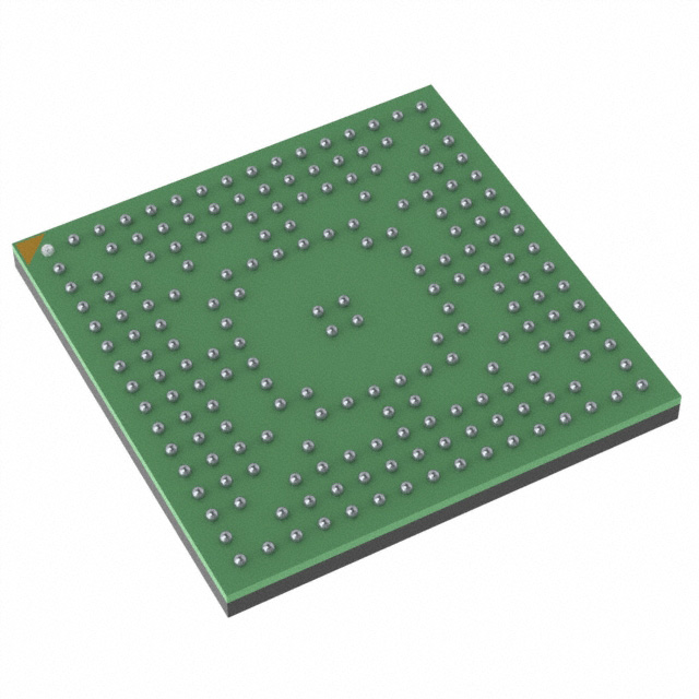


 工商网监
湘ICP备2023018690号
工商网监
湘ICP备2023018690号

