SEC1110/SEC1210
Smart Card Bridge to USB and UART Interfaces
General Description
The SEC1110 and SEC1210 provide a single-chip
solution for a Smart Card bridge to USB and UART
interfaces. These bridges are controlled by an
enhanced 8051 micro controller and all chip peripherals are accessed and controlled through the SFR or
XDATA register space. TrustSpanTM Technology
enables digital systems to securely communicate, process, move and store information on system boards,
across networks and through the cloud.
Feature Highlights
• Smart Card
- The SEC1110 provides one Smart Card interface and the SEC1210 provides two
- Fully compliant with ISO/IEC 7816, EMV 4.2/
4.3, ETSI TS 102 221 and PC/SC standards
- Versatile ETU rate generation, supporting
current and proposed rates (up to 826 Kbps)
- Full support of both T=0 and T=1 protocols
- Full-packet FIFO (261 bytes), for transmit
and receive
- Half-duplex operation (no software intervention required between transmit and receive
phases of exchange)
- Loose real-time response required of software (approximately 180 ms)
- Dynamically programmable FIFO threshold
with byte granularity
- Time-out FIFO flush interrupt, independent of
threshold
- Programmable Smart Card clock frequency
- UART-like register file structure
- Supports Class A, Class B, Class C, or Class
AB Smart Cards (1.8 V, 3.0 V and 5.0 V
cards)
- Automatic character repetition for T=0 protocol parity error recovery
- Automatic card deactivation on card removal
and on other system events, including persistent parity errors
- Internal procedure byte filtering for T=0 protocol
2013 - 2020 Microchip Technology Inc.
- Protocol timers (Guard, Timeout, and CWT)
for EMV-defined timing parameters
–Detection of an unresponsive card
–Activation/deactivation sequences
–Cold/warm resets
–Monitoring for all EMV timing constraints
–16-bit general purpose down counter for software
timing use
- Fully compliant ESD protection on card pins
• USB
- 12 Mbps USB operation compliant to the
USB 2.0 Specification
- Integrated USB 1.5 K pull-up resistor and
Dp,Dm series termination resistors
- Integrated USB devices controller with:
–8/16/32/64 byte control buffer
–Five 8/16/32/64 byte programmable (bulk/
interrupt) endpoint buffers
• 8051 Processor
- Reduced instruction cycle time (approximately 9 times 80C51)
- 9.6 MHz max clock speed
- Enhanced peripherals; three 16-bit timers,
watchdog timer, interrupt controller, JTAG
- OTP (One Time Programmable)
ROM : 16 KB RAM : 1.5 KB
• Boot ROM : 16 KB UART (SEC1210 only)
— Standard PC baud rates supported
— 3 M baud high-speed rate (not PC standard)
• SPI (SEC1210 only)
- Host capability with 12 MHz max performance
• General
- 5.0 V tolerance on user accessible IO pins
- Self-clocking internal oscillator, no external
crystal required
- 3.6 V - 5.5 V supply input
–Internal 4.8 V comparator disables Class A card
support if the input voltage is too low
- Available in commercial (0ºC to +70ºC) and
industrial (-40ºC to +85ºC) temperature
ranges
Applications
• USB Smart Card reader
• UART-based Smart Card reader
• Dual Smart Card reader
DS00001561D-page 1
�SEC1110/SEC1210
TO OUR VALUED CUSTOMERS
It is our intention to provide our valued customers with the best documentation possible to ensure successful use of your Microchip
products. To this end, we will continue to improve our publications to better suit your needs. Our publications will be refined and
enhanced as new volumes and updates are introduced.
If you have any questions or comments regarding this publication, please contact the Marketing Communications Department via
E-mail at docerrors@microchip.com. We welcome your feedback.
Most Current Data Sheet
To obtain the most up-to-date version of this data sheet, please register at our Worldwide Web site at:
http://www.microchip.com
You can determine the version of a data sheet by examining its literature number found on the bottom outside corner of any page.
The last character of the literature number is the version number, (e.g., DS30000000A is version A of document DS30000000).
Errata
An errata sheet, describing minor operational differences from the data sheet and recommended workarounds, may exist for current devices. As device/documentation issues become known to us, we will publish an errata sheet. The errata will specify the
revision of silicon and revision of document to which it applies.
To determine if an errata sheet exists for a particular device, please check with one of the following:
• Microchip’s Worldwide Web site; http://www.microchip.com
• Your local Microchip sales office (see last page)
When contacting a sales office, please specify which device, revision of silicon and data sheet (include -literature number) you are
using.
Customer Notification System
Register on our web site at www.microchip.com to receive the most current information on all of our products.
DS00001561D-page 2
2013 - 2020 Microchip Technology Inc.
�SEC1110/SEC1210
Table of Contents
1.0 Introduction ..................................................................................................................................................................................... 4
2.0 Block Diagrams ............................................................................................................................................................................... 7
3.0 Pin Table ......................................................................................................................................................................................... 9
4.0 Pin Configurations ......................................................................................................................................................................... 11
5.0 Pin Descriptions ............................................................................................................................................................................ 13
6.0 Pin Reset States ........................................................................................................................................................................... 16
7.0 8051 Embedded Controller ........................................................................................................................................................... 19
8.0 EC External Interrupts ................................................................................................................................................................... 24
9.0 8051 Special Function Registers .................................................................................................................................................. 27
10.0 Smart Card Interface ................................................................................................................................................................... 46
11.0 USB Controller Description ......................................................................................................................................................... 92
12.0 GPIO and LED Interface ........................................................................................................................................................... 117
13.0 Two Pin Serial Port (UART) ...................................................................................................................................................... 132
14.0 Serial Peripheral Interconnect (SPI1) - Host ............................................................................................................................. 145
15.0 Clock and Reset ........................................................................................................................................................................ 150
16.0 OTP ROM Test Interface .......................................................................................................................................................... 176
17.0 TEST Modes, JTAG, and XNOR .............................................................................................................................................. 187
18.0 DC Parameters ......................................................................................................................................................................... 188
19.0 8051 Timers .............................................................................................................................................................................. 197
20.0 Timing Diagrams ....................................................................................................................................................................... 206
21.0 Package Outlines
................................................................................................................................................................................................. 208
Appendix A: Acronyms, Definitions and Conventions ....................................................................................................................... 210
Appendix B: References ................................................................................................................................................................... 213
Appendix C: Revision History ........................................................................................................................................................... 214
The Microchip Web Site .................................................................................................................................................................... 216
Customer Change Notification Service ............................................................................................................................................. 216
Customer Support ............................................................................................................................................................................. 216
Product Identification System ........................................................................................................................................................... 217
2013 - 2020 Microchip Technology Inc.
DS00001561D-page 3
�SEC1110/SEC1210
1.0
INTRODUCTION
The SEC1110 and SEC1210 provide a single-chip solution for a Smart Card bridge to USB and UART interfaces. These
bridges are controlled by an enhanced 8051 micro controller and all chip peripherals are accessed and controlled
through the SFR or XDATA register space.
1.1
Features
• Smart Card
- Fully compliant with standards: ISO/IEC 7816, EMV 4.2/4.3, ETSI TS 102 221 and PC/SC
- Versatile ETU rate generation, supporting current and proposed rates (to 826 Kbps and beyond)
- Full support of both T=0 and T=1 protocols
- Full-packet FIFO (261 bytes), for transmit and receive
- Half-duplex operation, with no software intervention required between Transmit and Receive phases of an
exchange
- Very loose real-time response required of software: approximately 180 ms worst case
- Dynamically programmable FIFO threshold, with byte granularity
- Time-out FIFO flush interrupt, independent of threshold
- Programmable Smart Card clock frequency
- UART-like register file structure
- Supports Class A, Class B, Class C, or Class AB Smart Cards (all 1.8 V, 3.0 V and 5.0 V cards)
- Automatic character repetition for T=0 protocol parity error recovery
- Automatic card deactivation on card removal and on other system events, including persistent parity errors
- Internal procedure byte filtering for T=0 protocol
- Protocol timers (guard, time-out and CWT) for EMV-defined timing parameters
-
Detection of an unresponsive card
Activation/deactivation sequences
Cold/warm resets
Monitoring for all EMV timing constraints
16-bit general purpose down counter for software timing use
- Fully compliant ESD protection on card pins per JESD22-A114D (March 2006) and JESD22-A115A “Machine
Model” from AN1181
- Fully EMV compliant, internal signal current limits
- 3.3 V internal operation with 5.0 V tolerant buffers where required
- Self-contained management of Smart Card power:
-
SC1_VCC and SC2_VCC, supply output
Regulator for 1.8 V, 3.0 V, and 5.0 V from supply input
Current limiter with over-current sense interrupt (short circuit detect)
Hardware-ensured, compliant deactivation sequence on card removal
Synchronous card support
• USB
- 12 Mbps USB operation compliant with the USB 2.0 Specification
- Integrated USB 1.5 K pull-up resistor
- Integrated Series resistors on USB_DP, USB_DM
- Integrated USB devices controller with:
- 8/16/32/64 byte control endpoint 0 buffer
- Five 8/16/32/64 byte programmable (bulk/interrupt) endpoint buffers
• 8051
- Reduced instruction cycle time (approximately 9 times 80C51)
- 9.6 MHz max clock speed
- Enhanced peripherals: two 16-bit timers, watch dog timer, interrupt controller, JTAG
- 16 KB One Time Programmable (OTP) ROM
- 1.5 KB RAM
- 4 KB (SEC1100/SEC1200)/ 16KB (SEC1110/SEC1210) ROM
DS00001561D-page 4
2013 - 2020 Microchip Technology Inc.
�SEC1110/SEC1210
• UART
- Standard PC (9600, 19200, 38400 and 115200) baud rates supported
- 3 M baud high-speed rate (non-PC standard)
• SPI
- Host capability with 12 MHz max performance
• General
- 5.0 V tolerance on user accessible IO pins
- Self-clocking internal oscillator, no external crystal required
- 3.6 V-5.5 V supply input
- Internal 4.8 V comparator disables Class A card support if the input voltage is too low
1.2
Smart Card Subsystem
The SEC1110 and SEC1210 are fully compliant with the prevailing Smart Card standards: ISO7816, EMV, and PC/SC.
It meets and exceeds all existing requirements for communication bit rate (ETU duration) and includes support for proposed bit rates up to 826 Kbps. Signal levels and current limits are also fully compliant.
The Smart Card power is regulated and switched internally, supporting all 5.0 V, 3.0 V, and 1.8 V Smart Cards (classes
A, B, and C, respectively). Over-current protection is provided, and a detected over-current condition is available as an
interrupt. The required standard activation and deactivation sequences are provided with software interaction. However,
deactivation is handled in hardware as the card is being removed. This scenario ensures the required sequence regardless of software participation. If the system clock is inactive at the time, the card movement is detected asynchronously,
and the Wake-On Event feature is used to re-start the system clock so that the de-activation sequence can continue.
Interface signals to the Smart Card are designed to meet both standard drive levels and current limitations internally,
requiring no external series resistors. ESD protection on these signals meets the full standard requirements.
The device is a superset of the familiar 16450 UART architecture, with extensions in the form of a larger FIFO, specialized state machines for T=0 protocol parsing, automatic half-duplex turnaround at the completion of a transmitted message, and a specially-designed set of timers to enforce standards compliance in timing (as required of a terminal by the
ISO7816 and EMV standards).
With the full-packet-depth FIFO on-chip, software is almost totally excluded from real-time requirements. It loads an outgoing message into the FIFO, triggers the transfer, and reads the returned data at any time after it becomes available.
The reset sequence (cold or warm) is equally hands-off: software sets up the sequence and activates the reset, and is
alerted when the ATR message has been received (via the FIFO Threshold Interrupt). The threshold is dynamically programmable with byte granularity, so that threshold interrupts can be received at various stages in the processing of a
message of initially unknown length (such as ATR).
For detecting data time-outs, and for other mandatory timing tasks having to do with communication with a Smart Card,
a set of three protocol timers is provided:
• Time-out timer, for monitoring the standard WWT, BWT and WTX time-out intervals
• CWT timer, for monitoring the T=1 CWT time-out interval
• Guard timer, for ensuring the BGT and EGT transmission intervals, with special usage during a Reset sequence.
A separate general purpose timer is provided for software driver use.
Synchronous card support using GPIOs controlled via registers in the Smart Card device.
2013 - 2020 Microchip Technology Inc.
DS00001561D-page 5
�SEC1110/SEC1210
1.3
USB Subsystem
The USB Subsystem is made up of the following 3 functional blocks
• FS USB PHY
• USB Device Controller (UDC)
• Interface Bridge with USB endpoint buffers
FIGURE 1-1:
USB SUBSYSTEM BLOCK
USB D+
USB
FS
PHY
USB 1.1
Device Controller
USB D-
1.3.1
Interface
Bridge
+
Endpoint
Buffers
XDATA
Interrupt
FS USB PHY AND DEVICE CONTROLLER
The FS USB PHY contains the D+ pull-up resistor and handles the reception of USB data. The D+ and D- signals are
passed through the differential receiver (which is external to the device controller core) to get a single-ended bit stream.
The device controller has a digital phase-locked loop (DPLL) to extract the clock and data information. The clock and
data are passed to the SIE (serial interface engine) block to identify the sync pattern and for NRZI-NRZ conversion. This
NRZ data is then passed through a bit-stripper which strips off excessive inserted zeros. The data stream is passed
through a PID decoder and checker to identify different PID’s. The SIE block handles the protocol according to the type
of PID and the endpoint to which the current transaction is addressed. If it is a data PID, the serial data is assembled
into byte format and the received data is CRC is checked, then put into a one-byte buffer. The protocol layer takes the
data from the buffer and forwards it to the Interface Bridge. On control transfers to endpoint 0, the protocol layer forwards
the transfers to the endpoint block. If the application violates the data transfer protocol during the transfer of data from
the buffer to the application bus, the protocol layer controls the SIE to recover from this error.
1.3.2
INTERFACE BRIDGE AND ENDPOINT BUFFERS
These act as the interface between the 8051 micro controller and the USB device controller. The USB endpoint buffers
are memory mapped on the 8051 XDATA bus. A simple buffer scheme is employed, which assigns a single/ping-pong
buffer to each USB endpoint for ease of software control. Each buffer must be cleared before the next data transfer can
be started.
When USB OUT data is received, it is placed into the appropriate OUT endpoint buffer and the 8051 is signaled with an
interrupt (polling is also available)
When an IN request is received, the 8051 is signaled with an interrupt and the 8051 will transfer data to the appropriate
IN endpoint buffer and set a ready flag. The data will automatically be encoded for transfer over the USB bus.
1.4
Power Management Unit
The programmable clock divider supports division of the 48 MHz main clock. Additionally it enables power down under
program or hardware control. Exit from power down is accomplished through a single input pin. The power management
methods employed will enable a USB Suspend current of 200 A typical (400 A typical including Rpu current). In STOP
Mode, 1 A is the maximum current for a bare bones design.
DS00001561D-page 6
2013 - 2020 Microchip Technology Inc.
�SEC1110/SEC1210
2.0
BLOCK DIAGRAMS
FIGURE 2-1:
SEC1110 BLOCK DIAGRAM
Reset
VDD33
1
1
Power On Reset
Power Fail Detect
D+
D-
2
3.0 V - 5.5 V or VBUS
1
USB/GPIO/Core
Regulators
3.3 V
1.2 V
Smart
Card
Power
Control
Smart
Card
Regulators
5.0 V
3.0 V
1.8 V
USB
XDATA
Device
Controller
ISO7816 /
Smart
Card
Interface
USB
PHY
1.5
KB
RAM
CLK_PWR
48 MHz
Oscillator
16
KB
OTP
ROM
4/16
KB
ROM
Smart Card 1
7 pins
8051
CPU
Watchdog
Timer
256 x 8
RAM
CPU Power
Management
CPU Clock
Management
Timer 0
External
Interrupts
On Chip
Debug
JTAG
Timer 1
6
6
Timer 2
4
GPIO
4
Miscellaneous
2013 - 2020 Microchip Technology Inc.
DS00001561D-page 7
�SEC1110/SEC1210
FIGURE 2-2:
SEC1210 BLOCK DIAGRAM
Reset
1
Power On Reset
Power Fail Detect
D+
D-
2
USB
PHY
USB
Device
Controller
3.0 V - 5.5 V or VBUS
1
1
USB/GPIO/Core
Regulators
3.3 V
1.2 V
Smart
Card
Regulators
5.0 V
3.0 V
1.8 V
Smart Card
Power
Control
Smart
Card
Regulators
5.0 V
3.0 V
1.8 V
CLK_PWR
1
3
Smart Card
Power
Control
16
KB
OTP
ROM
4/16
KB
OTP
ROM
Smart Card1
7 pins
6+3
8051
CPU
Watchdog
Timer
256 x 8
RAM
CPU Power
Management
CPU Clock
Management
Timer 0
External
Interrupts
On Chip
Debug
JTAG
SAM2
4
1
ISO7816 /
Smart
Card
Interface
XDATA
1.5 KB
RAM
48 MHz
Oscillator
VDD33
Timer 1
Timer 2
6
UART
16550
4
6
SPI1
4
GPIO
Miscellaneous 8
DS00001561D-page 8
2013 - 2020 Microchip Technology Inc.
�SEC1110/SEC1210
3.0
PIN TABLE
3.1
SEC1110 16-Pin QFN
TABLE 3-1:
SEC1110 16-PIN PACKAGE
SMART CARD (7 PINS)
SC1_VCC
SC1_C8
Sc1_rst_N
sc1_clk
SC1_PRSNT_N/
SC1_C4
sc1_io
JTAG_TMS
USB INTERFACE (2 PINS)
USB_DP
usb_DM
MISC (5 PINS)
RESET_N
SC_LED_ACT_N/
JTAG_TDO
TEST
JTAG_CLK
JTAG_TDI
DIGITAL, POWER (2 PINS)
VDD33
VDD5
TOTAL 16 (VSS - THERMAL SLUG)
3.2
SEC1210 24-Pin QFN
TABLE 3-2:
SEC1210 24-PIN PACKAGE
SMART CARD (7 PINS)
SC1_VCC
SC1_C8
Sc1_rst_N
sc1_clk
SC1_PRSNT_N/
SC1_C4
sc1_io
JTAG_TMS
SMART CARD 2/SECURITY AUTHENTICATION MODULE (5 PINS)
SC2_VCC
Sc2_rst_N
sc2_clk
sc2_io
SC2_PRSNT_N/
JTAG_TDI
USB INTERFACE (2 PINS)
USB_DP
usb_DM
SPI1/UART (4 PINS)
SPI1_MISO/RXD
SPI1_MOSI/TXD
SPI1_CLK/CTS_OUT
SPI1_CE/RTS_IN
MISC (4 PINS)
2013 - 2020 Microchip Technology Inc.
DS00001561D-page 9
�SEC1110/SEC1210
TABLE 3-2:
SEC1210 24-PIN PACKAGE
RESET_N
SC_LED_ACT_N/
JTAG_TDO
TEST
JTAG_CLK
DIGITAL, POWER (2 PINS)
VDD33
VDD5
TOTAL 24 (VSS - THERMAL SLUG)
Note:
The NC pins are “No Connects”. There are no NC pads in the Known Good Die (KGD).
DS00001561D-page 10
2013 - 2020 Microchip Technology Inc.
�SEC1110/SEC1210
PIN CONFIGURATIONS
RESET_N
16
USB_DM
10
TEST
USB_DP
11
9
VDD33
Thermal Slug
(must be connected to
VSS)
4
15
SC1_IO
JTAG_TDI
SEC1110
(Top View QFN-16)
3
14
SC1_C4
SC_LED_ACT_N/JTAG_TDO
2
13
SC1_C8
JTAG_CLK
12
SEC1110 16-PIN QFN PACKAGE
1
FIGURE 4-1:
VDD5
4.0
8
SC1_PRSNT_N/JTAG_TMS
7
SC1_VCC
6
SC1_RST_N
5
SC1_CLK
Indicates pins on the bottom of the device
2013 - 2020 Microchip Technology Inc.
DS00001561D-page 11
�SEC1110/SEC1210
VDD33
USB_DP
USB_DM
TEST
SPI1_MOSI/TXD
SPI1_CE/ RTS
17
16
15
14
13
SEC1210 24-PIN QFN PACKAGE
18
FIGURE 4-2:
JTAG_CLK
19
12
SPI1_CLK/CTS
SC_LED_ACT_N/JTAG_TDO
20
11
SPI1_MISO/RXD
SC2_PRSNT_N/JTAG_TDI
21
10
SC1_PRSNT_N/JTAG_TMS
RESET_N
22
SC2_IO
23
SC2_CLK
24
SEC1210
(Top View QFN-24)
1
2
3
4
5
6
SC2_RST_N
SC2_VCC
VDD5
SC1_C8
SC1_C4
SC1_IO
Thermal Slug
(must be connected to VSS)
9
SC1_VCC
8
SC1_RST_N
7
SC1_CLK
Indicates pins on the bottom of the device
DS00001561D-page 12
2013 - 2020 Microchip Technology Inc.
�SEC1110/SEC1210
5.0
PIN DESCRIPTIONS
This section provides a detailed description of each signal. The signals are arranged in functional groups according to
their associated interface.
An N at the end of a signal name indicates that the active (asserted) state occurs when the signal is at a low voltage
level. When the N is not present, the signal is asserted when it is at a high voltage level. The terms assertion and negation are used exclusively in order to avoid confusion when working with a mixture of active low and active high signals.
The term assert, or assertion, indicates that a signal is active, independent of whether that level is represented by a high
or low voltage. The term negate, or negation, indicates that a signal is inactive.
5.1
SEC1110 and SEC1210 Pin Descriptions
TABLE 5-1:
Name
SEC1110 AND SEC1210 PIN DESCRIPTIONS
Symbol
Buffer
Type
Description
SMART CARD INTERFACE
SC Reset
Output
SC1_RST_N/
GPIO2
Note 5-1
SC2_RST_N/
GPIO18
SC Clock Output
SC1_CLK/
GPIO1
GPIO2, GPIO18: These pins may alternatively be configured
as a general purpose I/O pins.
Note 5-1
SC2_CLK/
GPIO17
SC Data I/O
SC Voltage for
Card
SC1_IO/
GPIO0
SC1_RST_N, SC2_RST_N: A low pulse resets the card and
triggers an “answer to reset” (ATR) response message. This
pin should be held low when the interface is not active.
SC1_CLK, SC2_CLK: The clock reference for communication
with the flash media card. This pin should be held low when
the interface is not active.
GPIO1, GPIO17: These pins may alternatively be configured
as general purpose I/O pins.
Note 5-1
SC1_IO, SC2_IO: The bidirectional serial data pin, which
should be held low when the interface is not active.
SC2_IO/
GPIO16
GPIO0, GPIO16: These pins may alternatively be configured
as general purpose I/O pins.
SC1_VCC/
SC2_VCC
The voltage supply pin, where the output of the pin can be set
to 1.8, 3.0, or 5.0 volts, depending on the type of Smart Card
detected. These pins require an external1 F capacitor.
The same voltage must be applied to power SCx_RST#,
SCx_CLK, SCx_IO, SCx_C4, and SCx_C8 pins as digital
inputs.
SC Standard or
Proprietary Use
Contact
SC Present
SC1_C8
(SC1_SPU)/
Note 5-1
GPIO4
SC1_PRSNT_N/
JTAG_TMS/
TIMER0_IN/
GPIO6
This pin can alternatively be used as general purpose I/O pin.
I/O8PUD
SC1_C4
(SC1_FCB)/
GPIO3
2013 - 2020 Microchip Technology Inc.
SC1_PRSNT_N, SC2_PRSNT_N: Active-low signals used to
detect the Smart Card device. These pins have an internal
pull-up which can be activated by software to detect the Smart
Card device.
JTAG_TMS, JTAG_TDI: These pins can alternatively be
configured in debug mode by software.
SC2_PRSNT_N/
JTAG_TDI/
GPIO19
SC1_FCB
SC1_C8, SC1_SPU: These pins can be used for either
standard or proprietary use as an input and/or output.
GPIO6, GPIO19: These pins can alternatively be used as
general purpose I/O pins, or as the Timer 0 input pin.
Note 5-1
SC1_C4: This pin is to attach to C4 of the Smart Card for
cards that support Function Code.
GPIO3: This pin may alternatively be configured as a general
purpose I/O pin.
DS00001561D-page 13
�SEC1110/SEC1210
TABLE 5-1:
SEC1110 AND SEC1210 PIN DESCRIPTIONS (CONTINUED)
Symbol
Buffer
Type
SC_LED_ACT_N/
I/O8PUD
Name
SC Active
Indicator
JTAG_TDO/
Description
The driver for the active LED.
This pin can alternatively be configured in debug mode by
software.
TIMER2_T2EX/
GPIO5
This pin may alternatively be used as general purpose I/O pin,
or as the Timer 2 “t2ex” input pin.
USB INTERFACE
USB Bus Data
USB_DM,
USB_DP
I/O-U
These pins connect to the upstream USB bus data signals.
SPI1/UART INTERFACE (QFN24)
SPI1 Chip
Enable
SPI1_CE_N/
I/O8PUD
If the SPI1 interface is disabled, this pin must be driven high
in idle state by software.
RTS/
This pin can alternatively function as the UART RTS signal,
when UART is used instead of SPI1.
GPIO11
SPI1 Clock
SPI1 Data In
The active-low chip-enable output (Host mode).
SPI1_CLK/
This pin may also be used as a general purpose I/O pin.
I/O8PUD
The SPI1 clock output (Host mode).
CTS/
This pin can alternatively function as the UART CTS signal,
when UART is used instead of SPI1.
GPIO10
This pin can alternatively be used as a general purpose I/O
pin.
SPI_MISO/
I/O8PUD
The Host data in to the controller.
This pin must have a weak internal pull-down applied at all
times to prevent floating.
SPI1 Data Out
RXD/
This pin alternatively function as the UART RXD input signal,
when UART is used instead of SPI1.
GPIO8
This pin can alternatively be configured as a general purpose
I/O pin.
SPI_MOSI/
I/O8PUD
This is the Host data output from the controller.
This pin must have a weak internal pull-down applied when
used as input to prevent floating.
TXD/
This pin can alternatively function as the UART TXD output
signal, when UART is used instead of SPI1.
GPIO9
GPIO9: This pin can alternatively be used as a general
purpose I/O pin.
MISC
TEST
TEST
I/O8PUD
This signal is used for testing the chip. If the test function is
not used, this pin must be tied low externally.
RESET input
RESET_N
IS
This active low signal is used by the system to reset the chip
and enter STOP mode. The active low pulse should be at
least 1 s wide. This pin is an analog input signal with Vil=100
mV.
JTAG Clock
JTAG_CLK
I/O8PUD
This input pad is used for JTAG debugging and has a weak
pull down. It can be left floating or grounded when not used.
If the JTAG is connected, this signal will be detected high, and
the software disables the pull-up after reset.
GPIO 28
GPIO28
I/O8PUD
General Purpose I/O pin.
GPIO 29
GPIO29
I/O8PUD
General Purpose I/O pin.
GPIO 30
GPIO30
I/O8PUD
General Purpose I/O pin.
DS00001561D-page 14
2013 - 2020 Microchip Technology Inc.
�SEC1110/SEC1210
TABLE 5-1:
SEC1110 AND SEC1210 PIN DESCRIPTIONS (CONTINUED)
Buffer
Type
Name
Symbol
Description
VBUS 5V Power
VDD5
5.0 V (or VBUS) power input.
3.3V Analog
Power Output
VDD33
3.3 V analog power output for decoupling capacitor. This pad
requires an external 1 F capacitor.
DIGITAL / POWER / GROUND
Ground
VSS
Note:
All pins OTP_VPP_MON, OTP_VREF, OTP_VREFA, OTP_VREF_SA are NC’s.
Note 5-1
5.2
Ground reference
This pin has a unique function, detailed in Section 18.0, "DC Parameters," on page 188.
Buffer Type Descriptions
TABLE 5-2:
SEC1110 AND SEC1210 BUFFER TYPE DESCRIPTIONS
Buffer Type
Description
I
Input
IPU
Input with weak internal pull-up resistor
IS
Input with Schmitt trigger
I/O12
Input/output buffer with 12 mA sink and 12 mA source
I/O8PD
Input/output buffer with 8 mA sink and 8 mA source, with an internal weak
pull-down resistor
I/O8PU
Input/output buffer with 8 mA sink and 8 mA source with an internal weak
pull-up resistor
I/O8PUPD
Input/output buffer with 8 mA sink and 8 mA source, with a selectable pullup and pull-down resistors
I/OD8PU
Input/open drain output buffer with a 8 mA sink
I/O12PD
Input/output buffer with 12 mA sink and 12 mA source, with an internal weak
pull-down resistor
I/O12PU
Input/output buffer with 12 mA sink and 12 mA source with an internal weak
pull-up resistor
I/O12PUPD
Input/output buffer with 12 mA sink and 12 mA source, with a selectable
pull-up and pull-down resistors
I/OD12PU
Input/open drain output buffer with a 12 mA sink
O12
Output buffer with a 12 mA sink and a 12 mA source
O12PD
Output buffer with 12 mA sink and 12 mA source, with a pull-down resistor
O12PU
Output buffer with 12 mA sink and 12 mA source, with a pull-up resistor
ICLKx
XTAL clock input
OCLKx
XTAL clock output
I/O-U
Analog input/output defined in USB specification
I-R
RBIAS
2013 - 2020 Microchip Technology Inc.
DS00001561D-page 15
�SEC1110/SEC1210
6.0
PIN RESET STATES
TABLE 6-1:
PIN RESET STATES
Hardware
Initialization
Voltage
Signal (V)
TABLE 6-2:
Firmware
Operational
RESET
VDD5
RESET
VSS
Time (t)
LEGEND FOR PIN RESET STATES TABLE
Symbol
Description
Y
Hardware enables function
0
Output low
1
Output high
--
Hardware disables function
Z
Hardware disables output driver (high impedance)
PU
Hardware enables pull-up
PD
Hardware enables pull-down
HW
Hardware controls function, but state is protocol dependent
(FW)
Firmware controls function through registers
VDD
Hardware supplies power through pin, applicable only to
CARD_PWR pins
none
Hardware disables pad
TABLE 6-3:
SEC1110 QFN 16-PIN RESET STATES
Reset State
Pin
Pin Name
Function
1
VDD5
5.0 V supply
2
SC1_C8
Smart Card1 C8 pin
Z
3
SC1_C4
Smart Card1 C4 pin
Z
4
SC1_IO
Smart Card1 IO pin
Z
DS00001561D-page 16
Output
PU/PD
Input
ANALOG
2013 - 2020 Microchip Technology Inc.
�SEC1110/SEC1210
TABLE 6-3:
SEC1110 QFN 16-PIN RESET STATES
Reset State
Pin
Pin Name
Function
Output
5
SC1_CLK
Smart Card1 CLK pin
Z
6
SC1_RST_N
Smart Card1 RST_N pin
Z
7
SC1_VCC
Smart Card1 Power supply
output 5.0V/3.3V/1.8V
Note 6-1
Note 6-2
8
SC1_PRSNT_N/JTAG_TMS
GPIO input for Smart Card1
presence detect.
Z
9
TEST
Test mode pin
Z
10
USB_DM
USB D-
Z
11
USB_DP
USB D+
Z
12
VDD33
13
JTAG_CLK
JTAG clock pin
Z
14
SC_LED_ACT_N/JTAG_TDO
GPIO output for
Smart Card1 LED
Z
15
JTAG_TDI
JTAG data in pin
Z
16
RESET_N
Reset input
-
VSS
Package ground
TABLE 6-4:
3.3 V power supply output
PU/PD
Input
ANALOG
PD
Note 6-8
Note 6-3
Yes
Note 6-6
ANALOG
PD
Yes
Note 6-6
PD
Yes
Note 6-6
Note 6-4
Note 6-8
Z
ANALOG
Note 6-5
ANALOG
SEC1210 QFN 24-PIN RESET STATES
Reset State
Pin
Pin Name
Function
Output
1
SC2_RST_N
Smart Card2 RST_N pin
Z
2
SC2_VCC
Smart Card2 power supply
output 5.0V/3.3V/1.8V
Note 6-1
Note 6-2
3
VDD5
5.0 V supply
4
SC1_C8
Smart Card1 C8 pin
Z
5
SC1_C4
Smart Card1 C4 pin
Z
6
SC1_IO
Smart Card1 IO pin
Z
7
SC1_CLK
Smart Card1 CLK pin
Z
8
SC1_RST_N
Smart Card1 RST_N pin
Z
9
SC1_VCC
Smart Card1 Power supply
output 5.0V/3.3V/1.8V
Note 6-1
Note 6-2
10
SC1_PRSNT_N/JTAG_TMS
GPIO input for Smart Card1
presence detect.
Z
11
SPI1_MISO/RXD
GPIO pin for SPI1 data
Z
2013 - 2020 Microchip Technology Inc.
PU/PD
Input
ANALOG
ANALOG
ANALOG
DS00001561D-page 17
�SEC1110/SEC1210
TABLE 6-4:
SEC1210 QFN 24-PIN RESET STATES
Reset State
Pin
Pin Name
Function
Output
12
SPI1_CLK/CTS
GPIO pin for SPI1 clock
Z
13
SPI1_CE/RTS
GPIO pin for SPI1 chip enable
Z
14
SPI1_MOSI/TXD
GPIO pin for SPI1 data
Z
15
TEST
Test mode pin
Z
16
USB_DM
USB D-
Z
17
USB_DP
USB D+
Z
18
VDD33
19
JTAG_CLK
JTAG clock pin
Z
20
SC_LED_ACT_N/JTAG_TDO
GPIO output for
Smart Card1 LED
Z
21
SC2+PRSNT_N/JTAG_TDI
GPIO input for Smart Card1
presence detect.
Z
22
RESET_N
Reset input
23
SC2_IO
Smart Card2 IO pin
Z
24
SC2_CLK
Smart Card2 CLK pin
Z
-
VSS
Package ground
PU/PD
Input
PD
Yes
Note 6-6
Note 6-8
Note 6-3
ANALOG
PD
Yes
Note 6-6
PD
Yes
Note 6-6
Note 6-8
Note 6-8
Z
ANALOG
Note 6-5
ANALOG
Note 6-1
The Smart Card1 and Smart Card2 power supply output is powered down at reset state.
Note 6-2
The Smart Card1 and Smart Card2 power supply output requires an external 1.0 F capacitor.
Note 6-3
Internal voltage regulator output for USB, GPIO 3.3 V IO Supply. This pin requires an external 1.0 F
capacitor.
Note 6-4
A weak pull down is present on the TEST, JTAG_CLK, and JTAG_TDI pads. If JTAG is connected,
and this pad is pulled high, then the reset state of the pins 8 (JTAG_TMS), 13(JTAG_CLK),
14(JTAG_TDO), and 15(JTAG_TDI) functions in JTAG Mode. The weak pull-down can be disabled
after reset release by software.
Note 6-5
RESET_N is an analog input, which when low, powers down all internal voltage regulators and the
pads are in high impedance state. The pads function as input, including pull-ups pull-downs
functionality after internal 3.3V power (VDD33) is good.
Note 6-6
The TEST, JTAG_CLK, and JTAG_TDI/GPIO[19] values at internal power on reset release (after
RESET_N release) is captured in the chip to enter various functional or test modes.
Note 6-7
Smart Card2 power supply output is powered down at reset state.
Note 6-8
A weak pull-down is present on TEST, JTAG_CLK, and JTAG_TDI pads if JTAG is connected, and
this pad is pulled high. The reset state of the pins 10(JTAG_TMS), 19(JTAG_CLK), 20(JTAG_TDO),
and 21(JTAG_TDI) function in JTAG Mode. The weak pull-down can be disabled after reset release
by software.
Note 6-9
The LCD regulator LDO4 and Smart Card2 output is powered down at reset state.
DS00001561D-page 18
2013 - 2020 Microchip Technology Inc.
�SEC1110/SEC1210
7.0
8051 EMBEDDED CONTROLLER
The embedded controller used in the SEC1110 and SEC1210 is an R8051XC2 from Evatronix. The R8051XC2 is a high
performance 8-bit embedded processor. The processor core is a low gate count core, with low-latency interrupt processing that features:
• Single clock per machine cycle: an average of 2.12 machine cycles per instruction
• Industry standard MCS51 instruction set
• Dual Data Pointers (2 x DPTR)
The R8051XC2’s interrupt controller is closely integrated with the processor core to achieve low latency interrupt processing, incorporating the following features:
• 13 external interrupts
• 4 priority levels for each interrupt
The embedded controller provides low-cost debug solutions, including:
• JTAG port for debugging using EASE OCDS debugging
• Software and 4 hardware breakpoints
The R8051XC2 bus interfaces include:
•
•
•
•
256 bytes internal data memory RAM
Program Memory Write Mode
Supports 128 KB program memory space with banking
Supports 128 KB of external data memory space with banking
2013 - 2020 Microchip Technology Inc.
DS00001561D-page 19
�SEC1110/SEC1210
FIGURE 7-1:
R8051XC2 Block Diagram
OCDS
EASE on-chip
Debugging block and
JTAG Interface
R8051XC2
CPU
JTAG
Clkper Peripherals
Timer 0
256 Bytes IRAM
Timer 1
SFR
Registers
Timer 2
OTP
ROM
Watchdog
Timer
ROM
External
Interrupts
UDC
USB
SPI
Host
SPI1
16550
UART
UART
SmartCard1,
2*
SC1, SC2
SFR Mux
Engine Clock
Peripheral Clock
Engine Clock
Enable
Peripheral Clock
Enable
Reset
ref_clk
GPIO
ISR
8051-compatible
Power Management,
Reset & Wake-Up
Control Units
Oscillators
External
Memory
XDATA
SRAM
GPIO
SMSC Trace FIFO,
SPI XIP
SPI2
* SEC1210 only
CLK_PWR
.
7.1
Sleep/Power Management
The R8051XC2 has a power management control unit that generates clock enable signals for the main CPU and for
peripherals; serves Power Down Modes IDLE and STOP; and generates an internal synchronous reset signal (upon
external reset, watchdog timer overflow, or software reset condition). The IDLE Mode leaves the clock of the internal
peripherals running. Any interrupt will wake the CPU.
The STOP Mode turns off all internal clocks. The CPU will exit this state when an external interrupt (0 or 1)or reset
occurs and internally generated interrupts are disabled since they require clock activity.
The Wake-up From Power-Down Mode control unit services two external interrupts during power-down modes. They
can combinationally force the clock enable outputs back to active state so the clock generation can be resumed.
DS00001561D-page 20
2013 - 2020 Microchip Technology Inc.
�SEC1110/SEC1210
7.1.1
EC DATA MEMORY
The EC has 1.5 KB data memory that is accessed through the XDATA Bus which is implemented with static RAM and
organized as 1.5 K x 8 bits. The base address of the memory is 8000h in the EC address space and extends to location
85FFh.
7.1.2
EC OTP INSTRUCTION MEMORY
The primary instruction memory for the EC is a 16 Kx 8 bit OTP ROM memory, located at locations 0000h through 3FFFh
in the EC address space. There is also a 4 K x 8 bit ROM that is used to overlay the OTP memory when it has not been
programmed. A bit in the OTP disables the ROM overlay. The OTP memory is also mapped into the XDATA space when
the overlay is active so that the CPU can program the OTP from the USB bus.
7.2
EC Registers
TABLE 7-1:
CODE EXECUTION TRUTH TABLE
EXT_SPI_EN/
BOND[2]
CODE
EXECUTION
X
1
External SPI2
0
0
ROM
0
1
0
OTP
1
X
X
OTP
OTP_CFG.FORCE_OTP_ROM
OTP_CFG.OTP_ROM_EN
0
0
The truth table indicates which memory is mapped into the 8051 CODE space depending on the three signals ROM_EN,
defined in the OTP_CFG Register. OTP_ROM_EN, and the EXT_SPI_EN (BOND2 bond option).
7.3
EC Memory Map
TABLE 7-2:
CODE SPACE
Name
Address Range
INTERNAL ROM (4 K) (SEC1110 and SEC1210)
INTERNAL ROM (16 K) (later versions)
0000h-0FFFh
C000h-CFFFh (alias address range) (deprecated)
18000h-18FFFh (alias address range)
1A000h-1DFFFh (alias address range) (later
versions)
OTP ROM (16 K)
0000h-3FFFh
EXTERNAL SPI
0000-FFFFh
SRAM (1.5 K)
19000h-195FFh (alias address range)
2013 - 2020 Microchip Technology Inc.
DS00001561D-page 21
�SEC1110/SEC1210
TABLE 7-3:
XDATA SPACE RANGES
Name
Address Range
OTP ROM (Note 7-1)
0000h-7FFFh
SRAM (1.5 K)
8000h-85FFh
Smart Card1,2
9000h-93FFh
UART
9500h-95FFh
USB DEVICE CONTROLLER
9600h-96FFh
SPI2 CODE MAIN
9A00h-9A18h
GPIO
9C00h-9DFFh
CLK_PWR
A000h-A3FFh
OTP_TEST
A400h-A7FFh
SPI2 CODE MAIN (TRACE FIFO)
BFFEh-BFFFh
INTERNAL ROM (4 K) (SEC1110 and SEC1210)
INTERNAL ROM (16 K) (later versions)
C000h-CFFFh (alias address range) (deprecated)
18000h-18FFFh (alias address range)
1A000h-1DFFFh (alias address range) (later
versions)
Note 7-1
OTP ROM is only visible in the XDATA space if the Internal ROM is enabled (see Table 7-1).
There is 128 KB of program space available. The lower 32 KB always is mapped to 0000-7FFFh. The higher ranges
32 KB to 128 KB are accessed through a window at 8000h-FFFFh using the pagesel registers.The ROM and SRAM are
also mapped to address at 96 KB. This enables access to ROM code while executing from OTP_ROM. This also
enables downloading code to SRAM and executing for test modes.
TABLE 7-4:
CPU BOOT ADDRESS MAPPING
CPU CODE
MAPPED
ADDRESS[15:
0]
00000h-7FFFh
CPU UNMAPPED ADDRESS[16:0]
COMMENT
INTERNAL ROM
BOOTING
INTERNAL
OTP_ROM
BOOTING
EXTERNAL SPI
BOOTING
FORCE_OTP_ROM
=0
OTP_ROM_EN=0
(FORCE_OTP_RO
M=1) | (
EXT_SPI_EN=0 &
OTP_ROM_EN=1)
FORCE_OTP_ROM=
0&
EXT_SPI_EN=1
ROM=
00000h-00FFFh
OTP_ROM_16K=
00000h-03FFFh
EXT_SPI=
00000h-07FFFh
If size of internal ROM/
OTP_ROM/ External
SPI is less than 32KB,
then rest of the region
is reserved.
pagesel[2:0]=000 must
not be used.
Reserved=
(OTP_ROM_16K)
08000h-0FFFFh
EXT_SPI=
08000h-07FFFh
pagesel[1:0]=01
Upper 32K of
ROM/OTP_ROM/EXT_
SPI code execution
8000h-FFFFh
8000h-FFFFh
DS00001561D-page 22
pagesel[1:0]=10
32KB OTP_ROM code
execution
2013 - 2020 Microchip Technology Inc.
�SEC1110/SEC1210
TABLE 7-4:
CPU BOOT ADDRESS MAPPING
CPU CODE
MAPPED
ADDRESS[15:
0]
8000h-FFFFh
CPU UNMAPPED ADDRESS[16:0]
Reserved=
18000h-1FFFFh
ROM=
18000h-18FFFh
ROM=
18000h-18FFFh
SRAM_1.5K=
19000h-195FFh
SRAM_1.5K=
19000h-195FFh
SRAM_1.5K=
19000h-195FFh
Reserved=
(SRAM_1.5K)
19600h-19FFFh
Reserved=
(SRAM_1.5K)
19600h-19FFFh
Reserved=
(SRAM_1.5K)
19600h-19FFFh
In
SEC1110/SEC1210
ROM=
1A000h-1DFFFh else
Reserved=
1A000h-1FFFFh
In
SEC1110/SEC1210
ROM=
1A000h-1DFFFh else
Reserved=
1A000h-1FFFFh
In
SEC1110/SEC1210
ROM=
1A000h-1DFFFh else
Reserved=
1A000h-1FFFFh
2013 - 2020 Microchip Technology Inc.
COMMENT
pagesel[1:0]=11
SRAM code execution
DS00001561D-page 23
�SEC1110/SEC1210
8.0
EC EXTERNAL INTERRUPTS
8.1
General Description
The R8051XC2 is 80515-compatible and will be configured to support thirteen external interrupt sources and four priority levels. In addition, there are individual internal interrupt sources for the R8051XC2 configured peripherals such as
the timers and SPI1 interfaces. Each source has its own request flag(s). Each interrupt requested by the corresponding
flag can be individually enabled or disabled by dedicated enable bits in the SFRs.
8.2
Interrupt Summary
TABLE 8-1:
INTERRUPT VECTOR MAPPING
INTERRUPT
INTPUT/
VECTOR
SOURCE
DESCRIPTION
int_vect_03
ie0
External Interrupt 0 - all interrupts ORed except GPIOs
In SEC1110/SEC1210 version, the SPI1, Power Status interrupts will not
cause an ie0 interrupt.
int_vect_0B
t0_f0
Timer 0 overflow
int_vect_13
ie1
External Interrupt 1 - GPIO Port 0,1,2 interrupts
int_vect_1B
tf1_gate
Timer 1 overflow
int_vect_23
uart_int
Serial Port 0 Interrupt
int_vect_2B
unused
Reserved
int_vect_43
iex7_gate
External Interrupt 7 - Reserved
int_vect_4B
iex2_gate
External Interrupt 2 - SPI1 Interrupt
int_vect_53
EP3INT
External Interrupt 3 - Endpoint 3 Interrupt. Also is active for Timer2 crc/cc0
comparator output.
int_vect_5B
EP4INT
External Interrupt 4 - Endpoint 4 Interrupt. Also is active for Timer2 cc1
comparator output.
int_vect_63
USB_INT_REG
External Interrupt 5 - USB Interrupt. Also is active for Timer2 cc2 comparator
output.
In SEC1110/SEC1210, the Timer2 cc2 comparator output will not cause an
interrupt.
int_vect_6B
POWER_STS
External Interrupt 6 - Power status event. Also is active for Timer2 cc3
comparator output.
In SEC1110/SEC1210, the Timer2 cc3 comparator output will not cause an
interrupt.
int_vect_83
unused
External Interrupt -Reserved
int_vect_8B
EP1INT
External Interrupt 8 - Endpoint 1 Interrupt
int_vect_93
EP2INT
External Interrupt 9 - Endpoint 2 Interrupt
int_vect_9B
EP5INT
External Interrupt 10 - Endpoint 5 Interrupt
int_vect_A3
EP0INT
External Interrupt 11 - Endpoint 0 Interrupt
int_vect_AB
iex12
External Interrupt 12 - Smart Card1 and Smart Card2 Interrupt
Note:
In SEC1110/SEC1210 version, External Interrupts 4, 5, and 6 are not active when TImer2 comparator outputs for cc1, cc2, and cc3 respectively are active. This Anomaly 24 is fixed in later versions.
DS00001561D-page 24
2013 - 2020 Microchip Technology Inc.
�SEC1110/SEC1210
8.3
EC ISR
The Interrupt Service Routine (ISR) unit, is a subcomponent responsible for interrupt handling. It receives up to 19 interrupt requests. Each of the interrupt sources can be individually enabled or disabled by the corresponding enable flag in
the ien0, ien1, ien2, and ien4 SFR registers. Additionally all interrupts can be globally enabled or disabled by the ea flag
in the ien0 Special Function Register.
All interrupt sources are divided into 6 interrupts groups. The definition of each group is shown in Table 8-2.
TABLE 8-2:
INTERRUPT PRIORITY GROUPS
Highest Priority in Group
GROUP
INTERRUPT
VECTOR
INTERRUPT
ENABLE BIT
NAME(BIT)
Lowest Priority in
Group
INTERRUPT
VECTOR
INTERRUPT
ENABLE BIT
INTERRUPT
VECTOR
INTERRUPT
ENABLE BIT
INTERRUPT
VECTOR
INTERRU
PT
ENABLE
BIT
Group0
int_vect_03
(External
Interrupt 0 - all
interrupts
ORed except
GPIOs)
ien0(0)
int_vect_83
(unused)
ien2(0)
int_vect_43
(External
Interrupt 7 reserved)
ien1(0)
Group1
int_vect_0B
(Timer 0
Interrupt)
ien0(1)
int_vect_8B
(External
Interrupt 8 Endpoint 1)
ien2(1)
int_vect_4B
(External
Interrupt 2 SPI1
Interrupt)
ien1(1)
Group2
int_vect_13
(External
Interrupt 1 GPIO 0,1,2)
ien0(2)
int_vect_93
(External
Interrupt 9 Endpoint 2)
ien2(2)
int_vect_53
(External
Interrupt 3Endpoint 3)
ien1(2)
Group3
int_vect_1B
(Timer 1
Interrupt)
ien0(3)
int_vect_9B
(External
Interrupt 10 Endpoint 5)
ien2(3)
int_vect_5B
(External
Interrupt 4Endpoint 4)
ien1(3)
Group4
int_vect_23
(16550 UART
Interrupt)
ien0(4)
int_vect_A3
(External
Interrupt 11 Endpoint 0)
ien2(4)
int_vect_63
(External
Interrupt 5USB
Interrupt)
ien1(4)
Group5
int_vect_2B
(Timer 2
Interrupt)
ien0(5)
int_vect_AB
(External
Interrupt 12 Smart Card
1/2)
ien2(5)
int_vect_6B
(External
Interrupt 6 Power Status
Event)
ien1(5)
int_vect_EB
(reserved)
ien4(5)
Inside a group, hardware dictates the interrupt priority structure. Interrupt sources from the first column have the highest
priority, sources from second column have middle priority, and sources from last column have the lowest priority. The
interrupt priority inside the group cannot be changed, where there is also an interrupt priority structure between the
groups. Group0 has the highest priority and Group5 has the lowest. The priority between groups can be programmed
by changing priority level (priority level can be set from 0 to 3) that is assigned to each group. The priority level of an
interrupt group is defined by flags of the ip0 and ip1 SFRs. When the priority levels for two groups are programmed to
the same level, the priority among them is in the order, from high to low (Group0 down to Group5).
To determine which interrupt has the highest priority (which must be serviced in the first order) the following steps are
completed:
1.
2.
3.
From all groups, those with the highest priority level are chosen.
From those with the highest priority level, the one with the highest natural priority between the groups in chosen.
From the group with highest priority, the interrupt with the highest priority inside the group is chosen.
The currently running interrupt service subroutine can be interrupted only by interrupts with a higher priority level. No
interrupt with the same or lower priority level can interrupt the currently running interrupt service subroutine. Therefore
there can be a maximum of four interrupts in service at the same time.
2013 - 2020 Microchip Technology Inc.
DS00001561D-page 25
�SEC1110/SEC1210
The ISR block inserts two CPU clock cycle delays between an interrupt request sent to the ISR and an interrupt request
sent by ISR to the CPU. When the ISR sends an interrupt request to the CPU, it responds by executing an interrupt
acknowledge cycle.
The interrupt vector table is located at 0000h, which is in the Internal ROM or OTP.
8.4
Wake-up Interrupt Source Register
The R8051XC2 controller contains a WAKEUP feature that allows either the EXT0 or EXT1 Interrupt to wake-up the
processor from the STOP or IDLE Mode. Since the clocks to the processor will be stopped, the interrupt sources for
EXT0 and EXT1 must be combinatorial. An additional register will provide masking for the available wake-up sources.
FIGURE 8-1:
WAKE-UP INTERRUPT
USB Interface
USB_INT
EP0INT
USB_WU_INT
EP1INT
Endpoint DMA
EP2INT
EP3INT
EP4INT
EP5INT
CLK_PWR
SPI1_INT
SmartCard1/2
UART
POWER_STS_INT
SPI1_INT
EXT0_INT
SC_INT
UART_INT
8051
WAKEUPCTRL
GPIO_INT (ie1)
GPIO 0, 1, 2
EXT1_INT
WOE_GPIO_INT
WOE (CLK_PWR)
If the interrupt is active and the corresponding bit in the Wakeup Enable Register is set, then the EXT0 Interrupt will be
active. If in IDLE or STOP Mode, this will wakeup the 8051.
The External Interrupt 1 (EXT1_INT) is connected to GPIO (0,1,2) interrupts. For a GPIO interrupt to occur, the CPU
clock must be active. The rest of the interrupt sources are ORed and connected to External Interrupt 0 (EXT0_INT),
including WOE_GPIO_INT. Additionally, the wake on event GPIO interrupt can occur when the clocks are in Sleep
Mode. Hence, the software can exit CPU_STOP Mode by any of the external interrupts.
In the SEC1110/SEC1210 version, the GPIO block runs off cpu_clk, and if the 8051 is in CPU_IDLE state, the GPIO
debounce feature does not function, as cpu_clk is gated.
In subsequent revisions, if the OSC48_SETTLE_CLKS.A1_COMPATIBILITY bit is set, the GPIO block runs off cpu_per_clk.
Hence if the 8051 is in CPU_IDLE state, the GPIO debounce feature functions normally.
DS00001561D-page 26
2013 - 2020 Microchip Technology Inc.
�SEC1110/SEC1210
9.0
8051 SPECIAL FUNCTION REGISTERS
9.1
Special Function Registers Locations
The map of special function registers is shown below in Table 9-1. Some addresses are occupied, while others are not
implemented. Read and write access to addresses that are not implemented will have no effect.
TABLE 9-1:
HEX
SPECIAL FUNCTION REGISTER LOCATIONS
0X0
0X1
0X2
0X3
0X4
0X5
0X6
0X7
F8
HEX
FF
B
F0
SRST
E8
F7
EF
ACC
E0
SPSTA
SPCON
SPDAT
SPSSN
E7
D8
DF
D0
PSW
C8
T2CON
D7
CCEN
C0
IEN1
B8
CRCL
CRCH
TL2
TH2
CCL1
CCH1
CCL2
CCH2
CF
CCL3
CCH3
IP1
C7
BF
B0
B7
IEN0
A8
IP0
AF
A0
A7
98
IEN2
90
DPS
DPC
PAGESE
L
D_PAGE
SEL
97
TMOD
TL0
TL1
TH0
TH1
8F
SP
DPL
DPH
DPL1
DPH1
TCON
88
80
Note:
9F
WDTREL PCON
87
The boxes shaded regions are undefined registers.
9.1.1
ACCUMULATOR REGISTER – ACC
The Accumulator Register is used by most of the R8051XC2 instructions to hold the operand and to store the result of
an operation. The mnemonics for accumulator-specific instructions refer to accumulator as A, not ACC.
TABLE 9-2:
ACC
ACC
(SFR 0XE0 - RESET=0X00)
ACCUMULATOR
BIT
NAME
R/W
DESCRIPTION
7:0
A
R/W
Accumulator
2013 - 2020 Microchip Technology Inc.
DS00001561D-page 27
�SEC1110/SEC1210
9.1.2
B REGISTER – B
TABLE 9-3:
B REGISTER
B
(SFR 0XF0 - RESET=0X00)
B
BIT
NAME
R/W
DESCRIPTION
7:0
B
R/W
Used during multiplying and division instructions. It can also be used
as a scratch-pad register to hold temporary data.
9.1.3
PROGRAM STATUS WORD REGISTER – PSW
The PSW Register contains status bits that reflect the current state of the CPU.
Note:
The parity bit can only be modified by hardware by the state of ACC Register.
TABLE 9-4:
PROGRAM STATUS WORD REGISTER
PSW
(SFR 0XD0 - RESET=0X00)
STACK POINTER
BIT
NAME
R/W
DESCRIPTION
7
cy
R/W
Carry flag:
The carry bit in arithmetic operations and the accumulator for Boolean
operations.
6
ac
R/W
Auxiliary Carry Flag:
Set if there is a carry-out from 3rd bit of the accumulator in BCD
operations.
5
f0
R/W
General Purpose Flag 0:
Available for general use.
4
rs1
R/W
Register Bank Select Control Bit 1:
3
rs0
R/W
Register Bank Select Control Bit 0:
Used to select the working register bank.
Used to select the working register bank.
2
ov
R/W
Overflow Flag:
1
f1
R/W
General Purpose Flag 1:
Set in case of overflow in accumulator during arithmetic operations.
Available for general use.
0
p
R
Parity Flag:
Reflects the number of 1s in the accumulator.
1 : If the accumulator contains an odd number of 1s
0 : If the accumulator contains an even number of 1s
The state of the rs1 and rs0 bits selects the working register bank as outlined in Table 9-5.
TABLE 9-5:
REGISTER BANK LOCATIONS
rs1
rs0
SELECTED REGISTER BANK
LOCATION
0
0
Bank 0
(00H – 07H)
0
1
Bank 1
(08H – 0FH)
1
0
Bank 2
(10H – 17H)
1
1
Bank 3
(18H – 1FH)
DS00001561D-page 28
2013 - 2020 Microchip Technology Inc.
�SEC1110/SEC1210
9.1.4
STACK POINTER REGISTER – SP
TABLE 9-6:
STACK POINTER REGISTER
SP
(SFR 0X81 - RESET=0X07)
STACK POINTER
BIT
NAME
R/W
DESCRIPTION
7:0
SP[7:0]
R/W
Clock Divide Low Byte:
Points to the top of the stack in the internal data memory space.
The Stack Pointer Register is used to store the return address of a program before executing an interrupt routine or
subprograms. The SP is incremented before executing a PUSH or CALL instruction, and it is decremented after executing a POP or RET(I) instruction (it always points the top of stack).
9.1.5
DATA POINTER AND DATA POINTER 1 REGISTERS – DPH, DPL AND DPH1, DPL1
TABLE 9-7:
DATA POINTER(1) LOW REGISTER
DPL
(SFR 0X82 - RESET=0X00)
DPL1
(SFR 0X84 - RESET=0X00)
DATA POINTER LOW
BIT
NAME
R/W
DESCRIPTION
7:0
DPL[7:0]
R/W
Data Pointer Low Byte
TABLE 9-8:
DATA POINTER(1) HIGH REGISTER
DPH
(SFR 0X83 - RESET=0X00)
DPH1
(SFR 0X85 - RESET=0X00)
DATA POINTER HIGH
BIT
NAME
R/W
DESCRIPTION
7:0
DPH[7:0]
R/W
Data Pointer High Byte
One of two data pointer registers can be accessed through DPL and DPH. The actual Data Pointer is selected by the
DPSEL Register.
These registers are intended to hold a 16-bit address in the Indirect Addressing Mode used by MOVX (move external
memory), MOVC (move program memory) or JMP (computed branch) instructions. They may be manipulated as a 16bit register or as two separate 8-bit registers. DPH holds the high byte and DPL holds the low byte of the indirect
address.
In general, the Data Pointer registers are used to access external code or data space (e.g., MOVC A,@A+DPTR or MOV
A,@DPTR, respectively).
The Data Pointer 1 Register can be accessed through DPL1 and DPH1. These SFR locations always refer to the
DPTR1, regardless of the actual data pointer selection by the DPS Register. This 16-bit register is used by all DPTRrelated instructions when the LSB of the DPS Register is set to 1, otherwise the DPTR is taken from DPH and DPL.
2013 - 2020 Microchip Technology Inc.
DS00001561D-page 29
�SEC1110/SEC1210
9.1.6
DATA POINTER SELECT REGISTER – DPS
TABLE 9-9:
DATA POINTER SELECT REGISTER
DPS
(SFR 0X92 - RESET=0X00)
DATA POINTER SELECT REGISTER
BIT
NAME
R/W
DESCRIPTION
7:1
Reserved
R
Always read as 0
0
dpsel0
R/W
Data Pointer Register Select:
0 : Data pointer 0 selected
1 : Data pointer 1 selected
The R8051XC2 contains up to two data pointer registers. Each of these registers can be used as 16-bit address source
for indirect addressing. The DPS Register serves for selecting the active data pointer register.
9.1.7
DATA POINTER CONTROL REGISTER – DPC
TABLE 9-10:
DATA POINTER CONTROL REGISTER
DPC
(SFR 0X93 - RESET=0X00)
DATA POINTER CONTROL REGISTER
BIT
NAME
R/W
DESCRIPTION
7:6
Reserved
R
Always read as 0
5:4
dpc[5:4]
R/W
Not used
3
dpc.3
R/W
Next Data Pointer Selection:
The contents of this field is loaded to the DPS Register bit 0 after
each MOVX @DPTR instruction.
Note:
2
dpc.2
R/W
This feature is not always enabled. Therefore, for each of
the DPS registers this field has to contain a different value
pointing to itself so that the auto-switching does not occur
with default (reset) values.
Auto-Modification Size:
When 0, the current DPTR is automatically modified by 1 after each
MOVX @DPTR instruction when dps.0=1. When 1, the current DPTR
is automatically modified by 2 after each MOVX @DPTR instruction
when dps.0=1.
1
dps.1
R/W
Auto-Modification Direction:
When 0, the current DPTR is automatically incremented after each
MOVX @DPTR instruction when dps.0=1. When 1, the current DPTR
is automatically decremented after each MOVX @DPTR instruction
when dps.0=1.
0
dps.0
R/W
Auto-Modification Enable:
When set, enables auto-modification of the current DPTR after each
MOVX @DPTR instruction
The R8051XC2 contains an optional DPTR-related arithmetic unit. It provides auto-increment/auto-decrement by 1 or
2, and auto-switching between active DPTRs. These functions are controlled by the DPC Register, where there are separate DPC register bits for each DPTR, to provide high flexibility in data transfers. The DPC Register address 0x93
points to the window where the actual dpc is selected using the DPS Register, same as for the DPTR.
DS00001561D-page 30
2013 - 2020 Microchip Technology Inc.
�SEC1110/SEC1210
9.1.8
PROGRAM MEMORY PAGE SELECTOR REGISTER – PAGESEL
TABLE 9-11:
PROGRAM MEMORY PAGE SELECTOR REGISTER
PAGESEL
(SFR 0X94 - RESET=0X01)
PROGRAM MEMORY PAGE SELECTOR REGISTER
BIT
NAME
R/W
DESCRIPTION
7:2
Reserved
R
Always read as 0
1:0
pagesel[1:0]
R/W
Provides an additional address for program memory in banking
scheme for memaddr[16:15]. Note that the default value is 1, to
provide normal address generation (logical address of 8000h equals
the physical address) when the PAGESEL Register is not written at
all after reset. The value of 0 should not be used since it causes the
banked area (logical address between 8000h-FFFFh) to overlap
physically with the common bank (0000h-7FFFh).
The program memory address bus (memaddr) can be extended up to 17 bits with the use of banking. When the CPU
targets addresses between 0000h and 7FFFh, the additional bits of the address bus are always 0, as the lowest 32 kB
is the common bank to store reset and interrupt vectors, and all common/shared/root subroutines. When the CPU
address is higher than 7FFFh of the program memory, the 2-bit contents of the PAGESEL Register is placed into the
memaddr[16:15] bits. The maximum number of pages is 4 (the common one at 0-32 kB, and 3 pages (banks) logically
visible at addresses between 32 kB-64 kB).
Note:
9.1.9
The 0 value of the PAGESEL Register should not be used since it leads to accessing the same physical
area at logical address space 8000h-FFFFh as 0000h-7FFFh. This causes the banked area to overlap with
the common bank.
DATA MEMORY PAGE SELECTOR REGISTER – D_PAGESEL
TABLE 9-12:
DATA MEMORY PAGE SELECTOR REGISTER
D_PAGESEL
(SFR 0X95 - RESET=0X01)
BIT
DATA MEMORY PAGE SELECTOR REGISTER
NAME
R/W
DESCRIPTION
7:2
Reserved
R
Always read as 0
1:0
d_pagesel[1:0]
R/W
Provides an additional address for data memory in banking scheme.
The default value is 1, to provide normal address generation (logical
address of 8000h equals the physical address) when the
D_PAGESEL Register is not written to after reset. The value of 0
should not be used since it causes the banked area (logical address
between 8000h-FFFFh) to overlap physically with the common bank
(0000h-7FFFh).
The external data memory address bus (memaddr) can be extended up to 17 bits with the use of banking. When the
CPU targets addresses between 0000h and 7FFFh, the additional bits of the address bus are always 0. When the CPU
addresses higher than 7FFFh of the program memory, the 2-bit contents of the D_PAGESEL Register is placed onto
the memaddr[16:15] bits. The maximum number of pages is 4 (the common one at 0-32 kB, and 3 pages (banks) logically visible at addresses between 32 kB-64 kB).
Note:
The 0 value of the D_PAGESEL Register should not be used since it leads to accessing the same physical
area at logical address space 8000h-FFFFh as 0000h-7FFFh. This causes the banked area to overlap with
the common bank.
2013 - 2020 Microchip Technology Inc.
DS00001561D-page 31
�SEC1110/SEC1210
9.1.10
TIMER/COUNTER CONTROL REGISTER – TCON
The TCON Register reflects the current status of R8051XC2 Timer 0 and Timer 1 and it is used to control operation of
these modules. The tf0, tf1 (Timer 0 and Timer 1 overflow flags), ie0 and ie1 (External Interrupt 0 and 1 flags) will be
automatically cleared by hardware when the corresponding service routine is called.
TABLE 9-13:
TIMER/COUNTER CONTROL REGISTER
TCON
(SFR 0X88 - RESET=0X00)
TIMER/COUNTER CONTROL REGISTER
BIT
NAME
R/W
DESCRIPTION
7
tf1
R/W
Timer 1 Overflow Flag:
Set by hardware when Timer 1 overflows. This flag can be cleared by
software and is automatically cleared when an interrupt is processed.
6
tr1
R/W
Timer 1 Run Control:
If cleared, Timer 1 stops.
5
tf0
R/W
Timer 0 Overflow Flag:
Set by hardware when Timer 0 overflows. This flag can be cleared by
software and is automatically cleared when an interrupt is processed.
4
tr0
R/W
Timer 0 Run Control:
If cleared, Timer 0 stops.
3
ie1
R/W
External Interrupt 1 Flag:
Set by hardware when an external interrupt int1 (edge/level,
depending on settings) is observed. It is cleared by hardware when
an interrupt is processed.
2
it1
R/W
External Interrupt 1 Type Control:
If set, External Interrupt 1 is activated at falling edge on input pin. If
cleared, External Interrupt 1 is activated at low level on input pin.
1
ie0
R/W
External Interrupt 0 Flag:
Set by hardware when an external interrupt int0 (edge/level,
depending on settings) is observed. Cleared by hardware when
interrupt is processed.
0
it0
R/W
External Interrupt 0 Type Control:
If set, External Interrupt 0 is activated at falling edge on input pin. If
cleared, External Interrupt 0 is activated at low level on input pin.
DS00001561D-page 32
2013 - 2020 Microchip Technology Inc.
�SEC1110/SEC1210
9.1.11
TIMER MODE REGISTER – TMOD
The TMOD Register is used in configuration of the R8051XC2 Timer 0 and Timer 1.
TABLE 9-14:
TIMER MODE REGISTER
TMOD
(SFR 0X89 - RESET=0X00)
TIMER MODE REGISTER
BIT
NAME
R/W
DESCRIPTION
7
gate
R/W
Timer 1 Gate Control:
If set, enables external gate control (pin int(1)) for Counter 1. When
int(1) is high, and tr1 bit is set, the Counter 1 is incremented every
falling edge on the t1 input pin.
6
c/t
R/W
Timer 1 Counter/Timer Select:
Selects the timer or counter operation. When set to 1, a counter
operation is performed; when cleared to 0, the Timer/Counter 1 will
function as a timer.
5
m1
4
m0
3
gate
R/W
Timer 1 Mode:
R/W
Timer 0 Gate Control:
Selects mode for Timer/Counter 1, as shown in Table 9-15 below.
If set, enables external gate control (pin int(0)) for Counter 0. When
int(0) is high, and tr0 bit is set, the Counter 0 is incremented every
falling edge on the t0 input pin
2
c/t
R/W
Timer 0 Counter/Timer Select:
Selects the timer or counter operation. When set to 1, a counter
operation is performed; when cleared to 0, the Timer/Counter 0 will
function as a timer.
1
m1
0
m0
R/W
Timer 0 Mode:
Selects the mode for Timer/Counter 0, as shown in Table 9-15 below.
TABLE 9-15:
TIMER/COUNTER MODES
M0
M1
MODE
FUNCTION
0
0
Mode 0
13-bit Counter/Timer, with 5 lower bits in the TL0 (TL1) Register and 8 bits
in TH0 (TH1) Register (for Timer 0 or Timer 1, respectively). Note, that
unlike in the 80C51, the 3 high-order bits of TL0 (TL1) are zeroed
whenever Mode 0 is enabled.
0
1
Mode 1
16-bit Counter/Timer
1
0
Mode 2
8-bit auto-reload counter/timer. The reload value is kept in TH0 (TH1),
while TL0 (TL1) is incremented every machine cycle. When TL0 (TL1)
overflows, a value from TH0 (TH1) is copied to TL0 (TL1).
1
1
Mode 3
For Timer 1: Timer 1 is stopped.
For Timer 0: Timer 0 acts as two independent 8-bit timers / counters – TL0,
TH0.
• TL0 uses the Timer 0 control bits and sets the tf0 flag on overflow.
• TH0 operates as the timer, which is enabled by the tr1 bit and sets the
tf1 flag on overflow.
2013 - 2020 Microchip Technology Inc.
DS00001561D-page 33
�SEC1110/SEC1210
9.1.12
TIMER 0,1,2 – TH0, TL0, TH1, TL1, TH2, TL2
TABLE 9-16:
TIMER 0, 1, AND 2 LOW BYTE
TL0
(SFR 0X8A - RESET=0X00)
TL1
(SFR 0X8B - RESET=0X00)
TL2
(SFR 0XCC - RESET=0X00)
TIMER 0/1/2 LOW BYTE
BIT
NAME
R/W
DESCRIPTION
7:0
TL0[7:0]/TL1[7:0]/ TL2[7:0]
R/W
Timer 0/ Timer 1/Timer 2 Low Byte
TABLE 9-17:
TIMER 0, 1, AND 2 HIGH BYTE
TH0
(SFR 0X8C - RESET=0X00)
TH1
(SFR 0X8D - RESET=0X00)
TH2
(SFR 0XCD - RESET=0X00)
TIMER 0/1/2 HIGH BYTE
BIT
NAME
R/W
DESCRIPTION
7:0
TH0[7:0]/ TH1[7:0]
R/W
TImer 0/ Timer 1/Timer 2 High Byte
•
•
•
•
•
•
TH0, TL0 registers reflect the state of Timer 0. TH0 holds higher byte and TL0 holds lower byte.
Timer 0 can be configured to operate as either a timer or counter.
TH1, TL1 registers reflect the state of Timer 1. TH1 holds the higher byte and TL1 holds the lower byte.
Timer 1 can be configured to operate as either a timer or counter.
TH2, TL2 registers reflect the state of Timer 2. TH2 holds the higher byte and TL2 holds the lower byte.
Timer 2 can be configured to operate in compare, capture or reload modes.
9.1.13
TIMER 2 CONTROL REGISTER – T2CON
The T2CON Register reflects the current status of the R8051XC2 Timer 2 and is used to control Timer 2 operation.
TABLE 9-18:
TIMER 2 CONTROL REGISTER
T2CON
(SFR 0XC8 - RESET=0X00)
TIMER 2 CONTROL REGISTER
BIT
NAME
R/W
DESCRIPTION
7
t2ps
R/W
Prescaler Select:
0 : Timer 2 is clocked with 1/12 of the oscillator frequency.
1 : Timer 2 is clocked with 1/24 of the oscillator frequency.
6
i3fr
R/W
Active edge selection for external interrupt “int3”, (used also as a
compare and capture signal):
0 : Falling edge
1 : Rising edge
5
i2fr
R/W
Active edge selection for external interrupt “int2”:
0 : Falling edge
1 : Rising edge
DS00001561D-page 34
2013 - 2020 Microchip Technology Inc.
�SEC1110/SEC1210
TABLE 9-18:
TIMER 2 CONTROL REGISTER (CONTINUED)
T2CON
(SFR 0XC8 - RESET=0X00)
TIMER 2 CONTROL REGISTER
BIT
NAME
R/W
DESCRIPTION
4
t2r1
R/W
Timer 2 Reload Mode Selection:
3
t2r0
0X : Reload disabled
10 : Mode 0
11 : Mode 1
2
t2cm
R/W
Timer 2 Compare Mode Selection:
0 : Mode 0
1 : Mode 1
1
t2i1
0
t2i0
R/W
Timer 2 Input Selection (t2i1, t2i0):
00 : Timer 2 stopped
01 : Input frequency f/12 or f/24
10 : Timer 2 is incremented by falling edge detection at pin “t2”.
11 : Input frequency f/12 or f/24 gated by external pin “t2”.
9.1.14
TIMER 2 COMPARE/CAPTURE ENABLE REGISTER – CCEN
The CCEN Register serves as a configuration register for the compare/capture unit associated with the Timer 2.
TABLE 9-19:
TIME 2 COMPARE/CAPTURE ENABLE REGISTER
CCEN
(SFR 0XC1 - RESET=0X00)
TIMER 2 CCEN REGISTER
BIT
NAME
R/W
DESCRIPTION
7
cocah3
R/W
Compare/Capture Mode for the CC3 Register:
6
cocal3
00 : Compare/capture disabled
01 : Capture on rising edge at pin TIMER2_CC0
10 : Compare enabled
11 : Capture on write operation into register CC3
5
cocah2
4
cocal2
R/W
Compare/Capture Mode for the CC2 Register:
00 : Compare/capture disabled
01 : Capture on rising edge at pin TIMER2_CC1
10 : Compare enabled
11 : Capture on write operation into register CC2
3
cocah1
2
cocal1
R/W
Compare/Capture Mode for the CC1 Register:
00 : Compare/capture disabled
01 : Capture on rising edge at pin TIMER2_CC2
10 : Compare enabled
11 : Capture on write operation into register CC1
1
cocah0
0
cocal0
R/W
Compare/Capture Mode for CRC Register
00 : Compare/capture disabled
01 : Capture on falling/rising edge at pin TIMER2_CC3 (not used)
10 : Compare enabled
11 : Capture on write operation into register CRCL
2013 - 2020 Microchip Technology Inc.
DS00001561D-page 35
�SEC1110/SEC1210
9.1.15
TIMER 2 COMPARE/CAPTURE REGISTERS – CC1, CC2, CC3
TABLE 9-20:
TIMER 2 COMPARE/CAPTURE REGISTERS LOW BYTE
CCL1
(SFR 0XC2 - RESET=0X00)
CCL2
(SFR 0XC4 - RESET=0X00)
CCL3
(SFR 0XC6 - RESET=0X00)
TIMER 2 COMPARE/CAPTURE 1,2,3 LOW BYTE
BIT
NAME
R/W
DESCRIPTION
7:0
CCL1[7:0]/ CCL2[7:0]/
CCL3[7:0]
R/W
TImer 2 Compare/Capture Register Low Byte
TABLE 9-21:
TIMER 2 COMPARE/CAPTURE REGISTERS HIGH BYTE
CCH1
(SFR 0XC3 - RESET=0X00)
CCH2
(SFR 0XC5 - RESET=0X00)
CCH3
(SFR 0XC7 - RESET=0X00)
TIMER 2 COMPARE/CAPTURE 1,2,3 HIGH BYTE
BIT
NAME
R/W
DESCRIPTION
7:0
CCH1[7:0]/ CCH2[7:0]/
CCH3[7:0]
R/W
TImer 2 Compare/Capture Register High Byte
Compare/Capture Registers (CC1, CC2, CC3) are 16-bit registers used in the operation of the compare/capture unit
associated with Timer 2. CCHn holds the higher byte and CCLn holds the lower byte of the CCn Register.
9.1.16
TIMER 2 COMPARE/CAPTURE REGISTERS – CRCH, CRCL
Compare/Capture Registers (CRCH, CRCL) are 16-bit registers used in the operation of the compare/capture unit associated with the Timer 2. CRCH holds higher byte and CRCL holds lower byte.
TABLE 9-22:
TIMER 2 COMPARE/CAPTURE REGISTERS
CRCL
(SFR 0XCA - RESET=0X00)
TIMER 2 COMPARE/CAPTURE 1,2,3 LOW BYTE
BIT
NAME
R/W
DESCRIPTION
7:0
CRCL[7:0]
R/W
TImer 2 Compare/Capture Register Low Byte
TABLE 9-23:
TIMER 2 COMPARE/CAPTURE REGISTER
CRCH
(SFR 0XCB - RESET=0X00)
TIMER 2 COMPARE/CAPTURE 1,2,3 HIGH BYTE
BIT
NAME
R/W
DESCRIPTION
7:0
CRCH[7:0]
R/W
TImer 2 Compare/Capture Register High Byte
DS00001561D-page 36
2013 - 2020 Microchip Technology Inc.
�SEC1110/SEC1210
9.1.17
WATCHDOG TIMER RELOAD REGISTER – WDTREL
The WDTREL Register holds the reload value of 7 high-order bits of the watchdog timer. It also configures the frequency
prescaler for the watchdog timer.
TABLE 9-24:
WATCHDOG TIMER RELOAD REGISTER
WDTREL
(SFR 0X86 - RESET=0X00)
DATA POINTER LOW
BIT
NAME
R/W
DESCRIPTION
7
WDTREL7
R/W
Prescaler Select:
When set, the watchdog is clocked through an additional divide-by16 prescaler.
6:0
WDTREL[6:0]
R/W
Watchdog Reload Value:
Reload value for the highest 7 bits of the watchdog timer. This value
is loaded to the watchdog timer when a refresh is triggered by a
consecutive setting of bits IEN0.wdt and IEN1.swdt).
9.1.18
INTERRUPT ENABLE 0 REGISTER – IEN0
TABLE 9-25:
INTERRUPT ENABLE 0 REGISTER
IEN0
(SFR 0XA8 - RESET=0X00)
INTERRUPT ENABLE 0 REGISTER
BIT
NAME
R/W
DESCRIPTION
7
eal
R/W
Interrupts Enable:
When set to 0 – all interrupts are disabled. Otherwise enabling each
interrupt is done by setting the corresponding interrupt enable bit.
6
wdt
R/W
Watchdog Timer Refresh Flag:
Set to initiate a refresh of the watchdog timer.
This bit must be set directly before IEN1.swdt is set to prevent an
unintentional refresh of the watchdog timer. The wdt bit is cleared by
hardware after the next instruction executed after the one that had
set this bit. Therefore, a watchdog refresh can only be done by
sequentially setting wdt followed by swdt.
5
et2
R/W
Timer 2 Interrupt Enable:
et2=0 : Timer 2 Interrupt is disabled.
et2=1 : and eal=1 Timer 2 Interrupt is enabled.
4
es0
R/W
16550 Serial Port 0 Interrupt Enable:
es0=0 : Serial Port 0 Interrupt is disabled.
es0=1 and eal=1 : Serial Port 0 Interrupt is enabled.
3
et1
R/W
Timer 1 Overflow Interrupt Enable:
et1=0 : Timer 1 Overflow Interrupt is disabled.
et1=1 and eal=1 : Timer 1 Overflow Interrupt is enabled.
2
ex1
R/W
External Interrupt 1 Enable (GPIO Ports 0,1,2):
ex1=0 : External Interrupt 1 is disabled.
ex1=1 and eal=1 : External Interrupt 1 is enabled.
2013 - 2020 Microchip Technology Inc.
DS00001561D-page 37
�SEC1110/SEC1210
TABLE 9-25:
INTERRUPT ENABLE 0 REGISTER (CONTINUED)
IEN0
(SFR 0XA8 - RESET=0X00)
INTERRUPT ENABLE 0 REGISTER
BIT
NAME
R/W
DESCRIPTION
1
et0
R/W
Timer 0 Overflow Interrupt Enable:
et0=0 : Timer 0 Overflow Interrupt is disabled.
et0=1 and eal=1 : Timer 0 Overflow Interrupt is enabled.
0
ex0
R/W
External Interrupt 0 Enable (or of all interrupts except GPIOs)
ex0=0 : External Interrupt 0 is disabled.
ex0=1 : and eal=1 External Interrupt 0 is enabled.
9.1.19
INTERRUPT ENABLE 1 REGISTER – IEN1
TABLE 9-26:
INTERRUPT ENABLE 1 REGISTER
IEN1
(SFR 0XB8 - RESET=0X00)
INTERRUPT ENABLE 1 REGISTER
BIT
NAME
R/W
DESCRIPTION
7
exen2
R/W
Timer 2 External Reload Interrupt Enable:
exen2=0 : Timer 2 External Reload Interrupt 2 is disabled.
exen2=1 and eal=1 : Timer 2 External Reload Interrupt 2 is enabled.
6
swdt
R/W
Watchdog Timer Start/Refresh Flag: set to activate/refresh the
watchdog timer.
When set directly after setting IEN0.wdt, a watchdog timer refresh is
performed. This bit is immediately cleared by hardware.
5
ex6
R/W
External Interrupt 6 Enable (Power Status Event):
ex6=0 : External Interrupt 6 is disabled.
ex6=1 and eal=1 : External Interrupt 6 is enabled.
4
ex5
R/W
External Interrupt 5 Enable (USB):
ex5=0 : External Interrupt 5 is disabled.
ex5=1 and eal=1 : External Interrupt 5 is enabled.
3
ex4
R/W
External Interrupt 4 Enable (Endpoint 4):
ex4=0 : External Interrupt 4 is disabled.
ex4=1 and eal=1 : External Interrupt 4 is enabled.
2
ex3
R/W
External Interrupt 3 Enable (Endpoint 3):
ex3=0 : External Interrupt 3 is disabled.
ex3=1 and eal=1 : External Interrupt 3 is enabled.
1
ex2
R/W
External Interrupt 2 Enable (SPI1):
ex2=0 : External Interrupt 2 is disabled.
ex2=1 and eal=1 : External Interrupt 2 is enabled.
0
ex7
DS00001561D-page 38
R/W
External Interrupt 7 Enable (Interrupt not connected to any source)
2013 - 2020 Microchip Technology Inc.
�SEC1110/SEC1210
9.1.20
INTERRUPT ENABLE 2 REGISTER – IEN2
TABLE 9-27:
INTERRUPT ENABLE 2 REGISTER
IEN2
(SFR 0X9A - RESET=0X00)
INTERRUPT ENABLE 2 REGISTER
BIT
NAME
R/W
DESCRIPTION
7:6
Reserved
R
Always read as 0
5
ex12
R/W
External Interrupt 12 Enable (Smart Card 1 or 2):
ex12=0 : External Interrupt 12 is disabled.
ex12=1 and eal=1 : External Interrupt 12 is enabled.
4
ex11
R/W
External Interrupt 11 Enable (Endpoint 0):
ex11=0 : External Interrupt 11 is disabled.
ex11=1 and eal=1 : External Interrupt 11 is enabled.
3
ex10
R/W
External Interrupt 10 Enable (Endpoint 5):
ex10=0 : External Interrupt 10 is disabled.
ex10=1 and eal=1 : External Interrupt 10 is enabled.
2
ex9
R/W
External Interrupt 9 Enable (Endpoint 2):
ex9=0 : External Interrupt 9 is disabled.
ex9=1 and eal=1 : External Interrupt 9 is enabled.
1
ex8
R/W
External Interrupt 8 Enable (Endpoint 1):
ex8=0 : External Interrupt 8 is disabled.
ex8=1 and eal=1 : External Interrupt 8 is enabled.
0
Reserved
2013 - 2020 Microchip Technology Inc.
R
Always read as 0
DS00001561D-page 39
�SEC1110/SEC1210
9.1.21
INTERRUPT PRIORITY REGISTERS – IP0, IP1
The 18 interrupt sources are grouped into 6 priority groups. For each of the groups, one of four priority levels can be
selected. It is achieved by setting appropriate values in the IP0 and IP1 registers.
The contents of the interrupt priority registers define the priority levels for each interrupt source according to the tables
below.
TABLE 9-28:
INTERRUPT PRIORITY 0 REGISTER
IP0
(SFR 0XA9 - RESET=0X00)
INTERRUPT PRIORITY 0 REGISTER
BIT
NAME
R/W
DESCRIPTION
7
Reserved
R/W
Always read as 0
6
wdts
R/W
Watchdog Timer Status Flag:
This bit is not set by hardware when the watchdog timer reset occurs.
If the RESET_SRC_WDOG bit in the CLKPWR_TEST4 Register is set,
it indicates that the chip reset was due to a watchdog timer reset.
5:0
-
R/W
Interrupt Priority:
Each bit together with the corresponding bit from the IP1 Register
specifies the priority level of the respective interrupt priority group.
TABLE 9-29:
INTERRUPT PRIORITY 1 REGISTER
IP1
(SFR 0XB9 - RESET=0X00)
BIT
NAME
INTERRUPT PRIORITY 1 REGISTER
R/W
DESCRIPTION
7:6
Reserved
R/W
Always read as 0
5:0
-
R/W
Interrupt Priority:
Each bit together with the corresponding bit from the IP0 Register
specifies the priority level of the respective interrupt priority group.
TABLE 9-30:
PRIORITY GROUPS
GROUP
CORRESPONDING
INTERRUPTS IN EACH GROUP
INTERRUPT BITS
0
IP1.0, IP0.0
Ext Interrupt 0 - or
of all interrupts
except GPIOs
1
IP1.1, IP0.1
Timer 0 Interrupt
External Interrupt 8
- Endpoint 1
External Interrupt 2
- SPI1 Interrupt
2
IP1.2, IP0.2
External Interrupt 1 External Interrupt 9
- GPIO port 0,1
- Endpoint 2
External Interrupt 3
- Endpoint 3
3
IP1.3, IP0.3
Timer 1 Interrupt
External Interrupt
10 - Endpoint 5
External Interrupt 4
- Endpoint 4
4
IP1.4, IP0.4
16550 UART
Interrupt
External Interrupt
11 - Endpoint 0
External Interrupt 5
- USB Interrupt
5
IP1.5, IP0.5
Timer 2 Interrupt
External Interrupt
12 - Smart Card
1/2
DS00001561D-page 40
Ext Interrupt 7 Reserved
Reserved
External Interrupt 6
- Power Status
Event
2013 - 2020 Microchip Technology Inc.
�SEC1110/SEC1210
TABLE 9-31:
PRIORITY LEVELS
IP1.X
IP0.X
PRIORITY LEVEL
0
0
Level 0 (lowest)
0
1
Level 1
1
0
Level 2
1
1
Level 3 (highest)
Note:
9.1.22
X represents the priority group
POWER CONTROL REGISTER – PCON
TABLE 9-32:
POWER CONTROL REGISTER
PCON
(SFR 0X87 - RESET=0X08)
POWER CONTROL REGISTER
BIT
NAME
R/W
DESCRIPTION
7
smod
R/W
This bit is not used.
6
wdt_tm
R/W
Watchdog Timer Test Mode Flag:
When set to 1, the fclk/12 divider at the input of the watchdog timer
is skipped.
5
isr_tm
R/W
Interrupt Service Routine Test Mode Flag:
When set to 1, the interrupt vectors assigned to Timer 0 and 1, Serial
Port 0 and 1, and SPI interfaces can be triggered only with the use
of external inputs of the core.
4
pmw
R/W
Program Memory Write Mode:
Setting this bit enables the Program Memory Write Mode.
3
p2sel
R/W
This bit is not used.
2
gf0
R/W
General Purpose Flag
1
stop
R/W
STOP Mode Control:
0
idle
R/W
Idle Mode Control:
Setting this bit activates the STOP Mode. This bit is always read as 0.
Setting this bit activates the IDLE Mode. This bit is always read as 0.
9.1.22.1
pmw
The MOVX instructions perform one of two actions depending on the state of pmw bit (PCON.4). The pmw bit selects the
standard or advanced behavior of the microcontroller during execution of MOVX instruction.
When the pmw is cleared or after reset, MOVX instructions allow read/write access to external data memory space. The
software can set the pmw bit to enable access to program memory space. Once pmw is set, MOVX data memory instructions become MOVX program memory instructions with 8 or 16-bit addressing modes. The software clears pmw to
switch back to normal MOVX behavior.
Setting or clearing pmw does not influence the execution of MOVC instruction and it does not change the behavior of
program memory reading.
9.1.22.2
CPU_IDLE
When the CPU_IDLE Mode is invoked, the ISR and other peripherals are clocked normally and interrupts are generated
normally. Therefore the irq signal coming from the ISR module can directly wake-up the CPU from CPU_IDLE Mode.
2013 - 2020 Microchip Technology Inc.
DS00001561D-page 41
�SEC1110/SEC1210
9.1.22.3
CPU_STOP
When the CPU_STOP Mode is invoked, neither the clkcpu nor clkper are working. The ISR module can’t generate an
interrupt since no peripherals are working. The only interrupts that may be accepted in the CPU_STOP Mode are External Interrupt 0 and 1. Hence before entering STOP Mode, the software must activate interrupts for the expected GPIO
port 0/1/2 interrupts (or USB Interrupt due to resume). An interrupt event would enable the clocks clkcpu, clkper to continue CPU processing.
9.1.23
SOFTWARE RESET REGISTER – SRST
TABLE 9-33:
SOFTWARE RESET REGISTER
SRST
(SFR 0XF7 - RESET=0X00)
SOFTWARE RESET REGISTER
BIT
NAME
R/W
DESCRIPTION
7:1
Reserved
R
Always read as 0
0
srstreq
R/W
Software Reset Request:
Writing a 0 to this bit will have no effect.
Single writing a 1 value to this bit will have no effect.
Double writing 1 value (in two consecutive instructions) will generate
an internal software reset.
Reading this bit will NOT provide feedback about the reset source.
The RESET_SRC_SRST bit in the CLKPWR_TEST4 Register if one
indicates that the chip reset was due to software reset request.
9.1.24
SPI1 SERIAL PERIPHERAL STATUS REGISTER – SPSTA
TABLE 9-34:
SPI1 SERIAL PERIPHERAL STATUS REGISTER
SPSTA
(SFR 0XE1 - RESET=0X00)
SERIAL PERIPHERAL (SPI1) STATUS REGISTER
BIT
NAME
R/W
DESCRIPTION
7
spif
R
Serial Peripheral Data Transfer Flag:
Set by hardware upon data transfer completion.
Cleared by hardware when data transfer is in progress. Can also be
cleared by reading the SPSTA.spif bit set, and then reading the
SPDAT Register.
6
wcol
R
Write Collision Flag:
Set by hardware upon write collision to SPDAT.
Cleared by hardware upon data transfer completion when no collision
has occurred. Can be also cleared by an access to the SPSTA
Register and an access to SPDAT Register.
5
sserr
R
Synchronous Serial Client Error Flag:
Set by hardware when SPI1_CE input is de-asserted before the end
of receive sequence. Cleared by disabling the SPI1 module (clearing
the SPCON.spen bit).
DS00001561D-page 42
2013 - 2020 Microchip Technology Inc.
�SEC1110/SEC1210
TABLE 9-34:
SPI1 SERIAL PERIPHERAL STATUS REGISTER
SPSTA
(SFR 0XE1 - RESET=0X00)
SERIAL PERIPHERAL (SPI1) STATUS REGISTER
BIT
NAME
R/W
DESCRIPTION
4
modf
R
Mode Fault Flag:
Set by hardware when the SPI1_CE pin level is in conflict with the
actual mode of the SPI_MS controller (configured as Host while
externally selected as Client).
Cleared by hardware when the ssn pin is at appropriate level. Can be
also cleared by software by reading the SPSTA Register with modf
set.
3:0
Reserved
R
Always read as 0
The SPSTA Register contains flags to signal data transfer complete, write collision, and inconsistent logic level on
SPI1_CE (Client select) pin (mode fault error).
9.1.25
SPI1 SERIAL PERIPHERAL CONTROL REGISTER – SPCON
The Serial Peripheral Control Register is used to configure the SPI module. It selects the Host clock rate, selects the
serial clock polarity and phase, enables the SPI1_CE input, and enables/disables the whole SPI1 module.
TABLE 9-35:
SPI1 SERIAL PERIPHERAL CONTROL REGISTER
SPCON
(SFR 0XE2 - RESET=0X14)
SERIAL PERIPHERAL (SPI1) CONTROL REGISTER
BIT
NAME
R/W
DESCRIPTION
7
spr2
R/W
Serial Peripheral Rate 2:
6
spen
R/W
Serial Peripheral Enable:
Together with spr[1:0] defines the clock rate in Host Mode.
When cleared, disables the SPI1 Interface. When set enables the
SPI1 Interface.
5
ssdis
R/W
SS Disable:
When cleared enables the SPI1_CE input. When set disables the
SPI1_CE input.
When ssdis is set, no SPSTA.modf interrupt request will be generated.
4
mstr
R/W
Serial Peripheral Host:
3
cpol
R/W
Clock Polarity:
When set configures the SPI1 as a Host.
When cleared, the SPI1_CLK is set to 0 in idle state. When set, the
SPI1_CLK is set to 1 in idle state.
2
cpha
R/W
Clock Phase:
When cleared, data is sampled when the SPI1_CLK leaves the idle
state (see SPCON.cpol). When set, data is sampled when the
SPI1_CLK returns to idle state (see SPCON.cpol).
1:0
spr[1:0]
R/W
Serial Peripheral Rate:
Together with spr2 specify the serial clock rate in Host Mode.
2013 - 2020 Microchip Technology Inc.
DS00001561D-page 43
�SEC1110/SEC1210
TABLE 9-36:
SPI1 TRANSFER RATE
SPR2
SPR1
SPR0
SERIAL PERIPHERAL RATE (SPI1_RATE)
0
0
0
spi1_clk/2
0
0
1
spi1_clk/4
0
1
0
spi1_clk/8
0
1
1
spi1_clk/16
1
0
0
spi1_clk/32
1
0
1
spi1_clk/64
1
1
0
spi1_clk/128
1
1
1
The Host clock is not generated (when SPCON.cpol=1, the SPI1_CLK output
is high level, otherwise is low level)
9.1.26
SPI1 SERIAL PERIPHERAL DATA REGISTER – SPDAT
The SPDAT Register is a read/write buffer for the “receive data” register. While writing to the SPDAT, data is placed
directly into the shift register (there is no transmit buffer).
TABLE 9-37:
SPI1 SERIAL PERIPHERAL DATA REGISTER
SPDAT
(SFR 0XE3 - RESET=0X00)
SERIAL PERIPHERAL (SPI1) DATA REGISTER
BIT
NAME
R/W
DESCRIPTION
7:0
spdat[7:0]
R/W
Serial Peripheral Data:
Reading returns the value located in the receive buffer, not the shift
register.
9.2
Special Function Registers Summary
The R8051XC can access up to 128 Special Function Registers. These registers can only be accessed directly.
TABLE 9-38:
SPECIAL FUNCTION REGISTERS SUMMARY
REGISTER
ADDRESS
DEFAULT
DESCRIPTION
SP
81h
07h
Stack Pointer
DPL
82h
00h
Data Pointer 0 Low
DPH
83h
00h
Data Pointer 0 High
DPL1
84h
00h
Data Pointer 1 Low
DPH1
85h
00h
Data Pointer 1 High
WDTREL
86h
00h
Watchdog Timer Reload Register
PCON
87h
00h
Power Control
TCON
88h
00h
Timer/Counter Control Register
TMOD
89h
00h
Timer Mode Register
TL0
8Ah
00h
Timer 0, Low Byte
TL1
8Bh
00h
Timer 1, Low Byte
TH0
8Ch
00h
Timer 0, High Byte
TH1
8Dh
00h
Timer 1, High Byte
DPS
92h
00h
Data Pointer Select Register
DS00001561D-page 44
2013 - 2020 Microchip Technology Inc.
�SEC1110/SEC1210
TABLE 9-38:
SPECIAL FUNCTION REGISTERS SUMMARY (CONTINUED)
REGISTER
ADDRESS
DEFAULT
DESCRIPTION
DPC
93h
00h
Data Pointer Control Register
PAGESEL
94h
01h
Program Memory Page Selector
D_PAGESEL
95h
01h
External Data Page Selector
IEN2
9Ah
00h
Interrupt Enable Register 2
IEN0
A8h
00h
Interrupt Enable Register 0
IP0
A9h
00h
Interrupt Priority Register 0
IP/IEN1
B8h
00h
Interrupt Priority Register/Enable Register 1
IP1
B9h
00h
Interrupt Priority Register 1
CCEN
C1h
00h
Compare/Capture Enable Register
CCL1
C2h
00h
Compare/Capture Registers – CC1 Low Byte
CCH1
C3h
00h
Compare/Capture Registers – CC1 High Byte
CCL2
C4h
00h
Compare/Capture Registers – CC2 Low Byte
CCH2
C5h
00h
Compare/Capture Registers – CC2 High Byte
CCL3
C6h
00h
Compare/Capture Registers – CC3 Low Byte
CCH3
C7h
00h
Compare/Capture Registers – CC3High Byte
T2CON
C8h
00h
Timer 2 Control Register
CRCL
CAh
00h
Compare/Capture Registers – CRC Low Byte
CRCH
CBh
00h
Compare/Capture Registers – CRC High Byte
TL2
CCh
00h
Timer 2, Low Byte
TH2
CDh
00h
Timer 2, High Byte
PSW
D0
00h
Program Status Word
IEN4
D1h
00h
Interrupt Enable Register 4
ACC
E0h
00h
Accumulator
SPSTA
E1h
00h
Serial Peripheral Status Register
SPCON
E2h
14h
Serial Peripheral Control Register
SPDAT
E3h
00h
Serial Peripheral Data Register
B
F0
00h
B Register
SRST
F7h
00h
Software Reset Register
2013 - 2020 Microchip Technology Inc.
DS00001561D-page 45
�SEC1110/SEC1210
10.0
SMART CARD INTERFACE
The SEC1110 provides one Smart Card Interface based on the ISO/IEC 7816 Standard, while the SEC1210 provides
two interfaces. The SEC1210, however, provides only one shared Packet FIFO. Hence, only one of the Smart Cards
can transfer data at any point of time, though both may be active and operational.
10.1
Interconnect to Smart Card Terminal
FIGURE 10-1:
SMART CARD 1 INTERCONNECT
TERMINAL
SC1_VCC (5.0 V/ 3.0 V/ 1.8 V)
SC1_RST_N/GPIO2
SC1_IO/GPIO0
SC1_CLK/GPIO1
SC1_C4/GPIO3
SEC1110/
SEC1210
1
5
2
6
3
7
4
8
SC1_C8/GPIO4
SC1_LED_ACT_N/GPIO5
SC1_PRSNT_N(GPIO6)
FIGURE 10-2:
S.A.M INTERFACE (SMART CARD 2)
TERMINAL
SC2_VCC
1
5
SC2_RST_N/ GPIO[18]
SC2_IO/ GPIO[16]
2
6
SC2_CLK/ GPIO[17]
3
7
4
8
SEC1210
SC2_PSNT_N/ GPIO[19]
DS00001561D-page 46
2013 - 2020 Microchip Technology Inc.
�SEC1110/SEC1210
10.2
Top Level of the Smart Card Interface
The Smart Card interface can alternatively be used as GPIOs. The synchronous ISO/IEC 7816-10 is supported by this
block by bit-addressable GPIOs (controls in the SC1 and SC2), or it can be configured to output the signals from the
GPIO block itself.
The muxing of the signals of the three different interfaces is shown in the figure below. The selection of whether the
GPIOs or the Smart Card logic controls the pins is controlled by auxiliary registers in GPIO block.
FIGURE 10-3:
SMART CARD1,2 INTERCONNECT
5 .0 /3 .0 /1 .8 V O L T
R EG U LATO R
5 .0 V
(F R O M
C LK_PW R
BLO C K)
V R EG _C TL
O C S2
O C S1
SC 2_V C C
PAD
SC 1_V C C
3 .0 V
PAD
1 .8 V
(F R O M
G P IO
BLO C K)
VDD 33
SC 1_PR SN T _N /
G P IO 6
PAD
SC 2_PR SN T _N /
G P IO 1 9
SC _LE D _SE L
PAD
G P IO 5
SC _L ED _A C T _N /
G P IO 5
PAD
GPIO6 (SC_PRSNT_N)
(For Auto Disconnect)
SC _LE D _A C T_N
SC 1_G P IO _E N
G P IO 2
G P IO 1
G P IO 0
G P IO 3
W RAPPER
G P IO 4
SC _LED _A C T_N
S C 1 _ R S T _ N /G P IO 2
PAD
S C 1 _ C L K /G P I O 1
SC1
UART
IP
(A sy n c )S C _ R S T _ N
S C 1 _ IO /G P IO 0
S C 1 _ F C B /S C 1 _ C 4 /
G P IO 3
(A sy n c )S C _ IO
SC _R ST _N
SC _C L K
S C _ IO
SC _SPU
(S y n c )S C _ C L K
XDATA
W RAPPER
G P IO
B lo c k m u x
SC _FC B
(S y n c )S C _ R S T _ N
SC
F IF O
(S y n c )S C _ IO
S C 2 _ G P IO _ E N
PAD
1 .8 /3 .0 /5 .0 V P o w e r P A D
PAD
1 .8 /3 .0 /5 .0 V IO P A D
PAD
3 .3 V IO P A D
PAD
1 .8 /3 .0 /5 .0 V IO P A D
SC_FC B
G P IO 1 8
SC _SPU
G P IO 1 7
G P I O 1 9 (S C _ P R S N T _ N )
(F o r A u to D isc o n n e c t)
G P IO 1 6
S C 2 _ R S T _ N /G P I O 1 8
S C 2 _ C L K /G P IO 1 7
(A sy n c )S C _ R S T _ N
S C 2 _ IO /G P IO 1 6
(A sy n c )S C _ C L K
PAD
PAD
PAD
(A sy n c )S C _ IO
SC m ux
SC _R ST _N
SC _C LK
S C _ IO
(S y n c )S C _ R S T _ N
(S y n c )S C _ C L K
SC2
S ync
In tfc
PAD
PAD
S C 1 _ S P U /S C 1 _ C 8 /
G P IO 4
SY N C _M O D E_SEL
SC _LED _A C T_N
SC2
UART
IP
PAD
(A sy n c )S C _ C L K
SC m ux
SC1
Sync
In tfc
PAD
G P IO
B lo c k m u x
SC _FC B
SC _SPU
(S y n c )S C _ IO
SY N C _M O D E_SEL
SC_FC B
SC _SPU
2013 - 2020 Microchip Technology Inc.
DS00001561D-page 47
�SEC1110/SEC1210
10.3
General Description
The Smart Card Interface serves as the core of a Terminal, or Interface Device (IFD), which communicates with an
insertable Smart Card, also called an Integrated Circuit Card (ICC).
The Smart Card interface is a UART-like interface that supports the ISO 7816 asynchronous protocols named T=0 and
T=1. It transmits and receives serial data via the SCx_IO (x is 1 or 2) signal pin. Each byte transmitted or received is
transferred as a character with a start bit, 8 data bits, a parity bit, and an amount of Guard Time (stop bits) that depends
on the protocol used and the declared characteristics of the card.
To initiate communication with the Smart Card, the Smart Card must be inserted into the terminal device. A mechanical
or electrical sensor will detect this event, pulling the SCx_PRSNT_N(GPIO6 or GPIO19) pin low to indicate that the electrical contacts are seated. The insertion of the card will cause a GPIO6 or GPIO19 Interrupt after the debounce period.
If the system is in suspend state, the GPIO transition will cause the system to be woken up first, followed by the interrupt
to the processor.
Once it is established that a Smart Card is present, firmware will use the VREG_CTL Register to apply power to the
card. Once the interface is powered, the terminal can initiate communication with the Smart Card by driving the SCx_RST_N pin low. There are two types of resets: a cold reset and a warm reset. The cold reset sequence is used immediately after power is applied to the interface: it generates the SCx_CLK output, sets the SCx_IO pin as an input with a
weak pull-up, and keeps the SCx_RST_N pin low (its initial state) for a defined period of time after the clock starts running. The warm reset only affects the SCx_RST_N pin, which is pulled low for a defined period of time: it requires that
the interface already be powered and a steady clock be already applied to the card. Bits have been provided in the
SC_ICR Register that may be controlled by software to initiate these sequences. When either of these resets terminates
(SCx_RST_N going high) the Smart Card will return a sequence of characters called the Answer to Reset (ATR) message as defined by ISO 7816-3. The Smart Card is required to respond to a reset sequence as shown in the cold reset
and warm reset timing diagrams (see Figure 10-10 and FIGURE 10-11: on page 62).
The first character of the ATR message, called TS, is interpreted by hardware in the SEC1110 and SEC1210, determining the bit encoding convention used by the card (direct or inverse) as defined by ISO 7816-3, which defines the polarity
and the order of the data and parity bits in the character. The TS byte, interpreted according to the convention it selects,
is placed into the FIFO, and data received from that point onward is assembled according to the selected convention
and loaded into the FIFO to be read by software.
The rest of the ATR response from the Smart Card returns the operational limits of the Smart Card. Software must interpret this response and set the SEC1110 and SEC1210 runtime registers accordingly. During the ATR message, data
will be received based on a default value of the bit time, called the Elementary Time Unit (etu). Two ATR parameters
named F and D are used to define a new etu time. Once this is determined, software can program the BRG Divisor
(SC_DLM and SC_DLL) and the sampling rate for the baud rate generator accordingly. The hardware divides the
Mhzsc1_clk (typically 48 MHz) system clock, by the BRG divisor and the sampling rate to determine the etu value (bit
time). The SCx_CLK frequency is generated by dividing the sc1_clk clock by the SC_CLK_DIV DIVISOR field. Software
will also set up the Extra Guard Time Register (SC_EGT), the Block Guard Time (SC_BGT) Register and the protocol
Mode (T=0 or T=1 Mode) to set the required amount of Guard Time between character transmissions.
A negotiation phase called PPS may occur, or communication may begin immediately using the parameters provided
by the card’s ATR message. In either case, all communication after the ATR message consists of individual exchanges,
in which the IFD transmits a block of data and the ICC responds with a return message. For this reason, and because
the response time from the ICC can be too short for software intervention, software will enable both the SEC1110 and
SEC1210 transmitter and receiver at the same time, and the receiver hardware will remain inactive until the transmission
phase of the exchange has completed.
An additional stop clock feature has been provided to hold the SCx_CLK output at a particular voltage level between
exchanges, as may be allowed by the card for power savings. Clock switching is glitch free.
Hardware protocol timers, set according to default timings, will monitor the Smart Card interface during the reset/ATR
sequence for an unresponsive or defective card, based on the EMV, ISO and PC/SC timing requirements. If the ATR
response is not received within the given time, or does not obey the required timings, a Timer Interrupt will result. The
software can then take corrective action or initiate the deactivation sequence to stop and power-down the card.
After the ATR sequence, the same set of hardware timers are used, based on ATR parameters EGT, CWT, BWT, and/or
WWT, to monitor timings for the subsequent data exchanges.
DS00001561D-page 48
2013 - 2020 Microchip Technology Inc.
�SEC1110/SEC1210
One of two protocols is selected, defined by a parameter T in the ATR message, and potentially negotiated in a PPS
exchange. The protocol T=0 is character-oriented, with parity error detection and re-transmission on a character-bycharacter basis. The protocol T=1 is block-oriented, with an error-free link layer based on block re-transmission, resembling the X.25 communication standard. In the T=1 protocol, both individual character parity and a block check field are
used to detect errors.
The SEC1110 and SEC1210 SC_FIFO is deep enough to hold an entire message of maximum length (259 bytes in
SEC1110/SEC1210 and 261 bytes in SEC1110/SEC1210). It transmits data, pre-loaded into the SC_FIFO, when the
transmit control bit is set by software. It immediately turns around, enabling the Receiver to put data received back into
the SC_FIFO. The SC_FIFO Threshold Interrupt is triggered by received data only, though a separate interrupt is available to signal when the transmit phase has ended. The hardware has significant knowledge of the protocol being implemented, and can be set up to filter out bytes that would lead to a message longer than the SC_FIFO depth.
After deactivation of the ICC, it is required to perform a block reset to the smart clock block using SC1_RESET or
SC2_RESET, or initialize all the registers to desired values.
10.4
Character Framing
The SEC1110 and SEC1210 meets the requirements for a character frame as defined by ISO 7816-3. The T=0 and T=1
protocol differ in the minimum amount of Guard Time: 2 etus for T=0, and 1 etu for T=1, which does not require a character-by-character parity error response.
Character parity is checked as each byte is received by hardware. If a parity error is detected when a byte is received,
the parity error status bit will be set. This status bit can be polled by software, or it can be programmed to generate an
interrupt and/or to deactivate the card in hardware. If character repetition is enabled (used in the T=0 protocol) the
SEC1110 and SEC1210 will pull the SCx_IO line low following a received parity error, for the duration of 1 etu as defined
by ISO 7816-3. If the card signals receipt with a parity error while the SEC1110 and SEC1210 is transmitting, it will repeat
the character up to 4 additional times. Whether transmitting or receiving, failure after 5 transmissions of the same character will cause a Parity Error Interrupt and/or hardware deactivation of the ICC.
Note:
Software should not try to initiate a RESYNCH until the transaction has completed, because the card may
still be trying to send data to the IFD. Timeout timers and an Activity Detection bit are provided to assist
software in this determination, in case of an error.
FIGURE 10-4:
Note:
T=0 MODE CHARACTER TRANSMISSION AND REPETITION DIAGRAM
Timing is measured in etus. 1 etu = time to transmit 1 bit. The default etu is equal to 372/f, where f is the
clock frequency.
2013 - 2020 Microchip Technology Inc.
DS00001561D-page 49
�SEC1110/SEC1210
TABLE 10-1:
CHARACTER FRAME FORMAT
TRANSMISSION
DEFINITION
Start Bit
The I/O signal is held low for the duration of one etu after the Guard Time before
transmitting data.
Data Byte
The 8 bits immediately following the start bit that represents a single character byte. The
logical value of the data byte transmitted is dependent on the convention selected by TS
of the ATR.
Direct Convention: logical 1 equals VCC and bits are transmitted LSB first.
Inverse Convention: logical 0 equals VCC and bits are transmitted MSB first.
Note:
Data received is interpreted according to the encoding convention selected by the
ICC.
Parity Bit
The parity bit is used for error detection. It is used to provide even parity, operating on 1
and 0 as defined by the convention. The parity bit itself is also represented with the same
polarity as the data field, according to the selected encoding convention.
Guard Time
The Guard Time is defined as the time between the transmission of the parity bit and the
next start bit transmitted. During this time, both the Transmitter and Receiver release the
bus. Only the Receiver is permitted to pull the bus low during this time (in all except T=1)
to indicate a parity error has occurred.
Guard time = minimum Guard Time + Extra Guard Time (N); for 0 N 254
Guard time = minimum Guard Time; for N=255.
T=0 (including ATR and PPS) requires a minimum Guard Time of 2 etus. T=1 requires a
minimum Guard Time of 1 etu. The minimum Guard Time is determined by whether T=0
or T=1 Mode is chosen in the Protocol Mode Register.
Extra Guard Time (N) is programmable from 0 to 254 etus, as requested by the card in
the ATR message. The default value is 0. The value of N received in the ATR should be
directly programmed in the EGT Register.
10.5
Clocking and Baud Rate Generation
The frequency of the SCx_CLK signal to the ICC, and the rate at which bits are transmitted and sampled, are determined
from the frequency of sc1_clk clock, which is a divided version of 48 MHz clock.
No other clock frequency is available in the SEC1110 and SEC1210.
10.5.1
CLOCK RATE GENERATION
The internal clock rate generator determines the frequency of the clock to be provided to the ICC on the SCx_CLK pin.
This is expressed in the least-significant 6 bits of the SC_CLK_DIV Register as a divisor on the system clock. To find
the correct value, the Fi value is read from the card, and Fmax is determined. The divisor is chosen such that SCx_CLK
is the highest possible frequency without violating the Fmax parameter. The frequency of the clock to the Smart Card
blocks is selected to be the minimum required to satisfy SCx_CLK frequency and the etu rate. This is done to lower
dynamic power dissipation of the block.
Frequency of clock to Smart Card 1 block is Fsc1_clk = 48 MHz / SC1_CLK_DIV.
Frequency of SC1_CLK pin = Fsc1_clk / DIVISOR[4:0]
10.5.2
ETU RATE GENERATION
The internal Baud Rate Generator (BRG) sets the duration of an etu (bit time). In the ATR message from the ICC, a
divisor term (F) and a multiplier term (D) come from two 4-bit values Fi and Di. (If the ICC does not provide these values,
the default is Fi=1 and Di=1, which specify a simple division by 372). The Fi and Di values are specified relative to the
SCx_CLK frequency. But within SEC1110 and SEC1210, this must be translated to a simple divisor of the system clock.
There are two components to this divisor: a Sampling Mode and a Divisor Latch value (DL). The divisor latch value is
held as a 16-bit value in the SC_DLL/SC_DLM register pair. The sampling mode is contained in the most-significant two
bits of the SC_CLK_DIV Register.
DS00001561D-page 50
2013 - 2020 Microchip Technology Inc.
�SEC1110/SEC1210
The value in the DLL/DLM registers is interpreted according to the separate Sampling Mode, held in the most-significant
two bits of the SC_CLK_DIV Register. The sampling mode is a pre-scaler and one of three valid settings:
• 00b : prescaler of 31
• 10b : prescaler of 16
• 01b : no prescaler. The divisor directly specifies the etu rate in units of the sc1_clk clock, and each bit is sampled
directly by that clock. This form gives better accuracy. Also, even in a non-standard application, it is not allowed to
specify fewer than 16 sample times per etu.
For example assume during ATR,TA bits 8~5 = 0010b (Fi=558), and bits 4~1 = 0011b (Di=4) then Fmax = 6 MHz, and
the desired divisor = 139.5.
This means:
• Fmax = 6 MHz (based on Fi)
• Desired divisor = 558/4 = 139.5
Desired baud rate = 4.8 MHz/139.5 = 34408.6 bps. This means based on a 48 MHz clock the divisor latch value must
be: 48 MHz/34408 = 1395. To set the SCx_CLK frequency close to Fmax, then SCx_CLK divisor (DIVISOR[4:0]) must
be set to 48 M/4.8 M = 10.
The single bit error due to the terminal’s sampling rate = (1 / 48 MHz) / (1 ETU) = (1/48e6) / (1/34408.6) = 0.071%. The
error accumulated over a byte (starting from START bit, 8 data bits, parity bit, pause sample) = 10 * 2% = 20%.
The maximum error allowed per bit is determined by maximum rise/fall times (8%), minimum sampling time (0.2 etu,
i.e., 20%), and maximum clock jitter (1% p-p).
When the Receiver samples, the maximum allowed error per bit = 0.2 etu/10 = 20.0% /10 = 2.00%
For some of the Fi/Di ratios, lower power consumption can be achieved by reducing the Smart Card block frequency,
while maintaining the maximum line rate. This requires operating within the maximum allowed error rate per bit.
10.5.3
RECOMMENDED ETU RATES AND SETTINGS
Table 10-2 lists the valid etu rates supported, and the recommended settings of the DL divisor (in the DLL/DLM registers) and the sampling field of the CLK Register that are used to select them.
The settings shown are for the maximum block frequency (48 MHz, i.e., SCx_CLK_DIV=1) to the Smart Card block to
reduce error to a minimum.
TABLE 10-2:
RECOMMENDED SETTINGS FOR VALID TA1 ETU RATES
FI
(DEC)
DI
(DEC)
FI/DI
(REAL)
SAMPLING
FIELD
(BINARY)
SCLK
(ACTUAL)
MHZ
DL DIVISOR
VALUE
(DECIMAL)
0
1
372
01
4.8
3720
12903.23
0
2
186
01
4.8
1860
25806.45
0.00%
0
3
93
01
4.8
930
51613.90
0.00%
BAUD RATE
(BITS/SEC)
BIT
ERROR (%)
0.00%
0
4
46.5
01
4.8
465
103226.81
0.00%
0
5
23.25
01
4.8
233
206008.58
0.22%
0
6
11.625
01
4.8
116
413793.10
-0.22%
0
7
5.813
01
4.8
58
827586.21
-0.22%
0
8
32
01
4.8
31
154838.71
0.00%
0
9
18.6
01
4.8
186
258064.52
0.00%
1
1
372
01
4.8
3720
12903.23
0.00%
1
2
186
01
4.8
1860
25806.45
0.00%
1
3
93
01
4.8
930
51613.90
0.00%
1
4
46.5
01
4.8
465
103226.81
0.00%
1
5
23.25
01
4.8
233
206008.58
0.22%
1
6
11.625
01
4.8
116
413793.10
-0.22%
1
7
5.813
01
4.8
58
827586.21
-0.22%
2013 - 2020 Microchip Technology Inc.
DS00001561D-page 51
�SEC1110/SEC1210
TABLE 10-2:
RECOMMENDED SETTINGS FOR VALID TA1 ETU RATES (CONTINUED)
FI
(DEC)
DI
(DEC)
FI/DI
(REAL)
SAMPLING
FIELD
(BINARY)
SCLK
(ACTUAL)
MHZ
DL DIVISOR
VALUE
(DECIMAL)
1
8
31
01
4.8
31
154838.71
0.00%
1
9
18.6
01
4.8
186
258064.52
0.00%
2
1
558
01
4.8
5580
8602.15
0.00%
2
2
279
01
4.8
2790
17204.30
0.00%
2
3
139.5
01
4.8
1395
34408.60
0.00%
2
4
69.75
01
4.8
698
68767.91
0.07%
2
5
34.875
01
4.8
349
137535.82
0.07%
2
6
17.438
01
4.8
174
275862.07
-0.22%
2
7
8.719
01
4.8
87
551724.14
-0.22%
2
8
46.5
01
4.8
465
103225.81
0.00%
2
9
27.9
01
4.8
279
172043.01
0.00%
3
1
744
01
4.8
7440
6451.61
0.00%
3
2
372
01
4.8
3720
12903.23
0.00%
3
3
186
01
4.8
1860
25806.45
0.00%
3
4
93
01
4.8
930
51612.90
0.00%
3
5
46.5
01
4.8
465
3
6
23.25
01
4.8
233
206008.58
3
7
11.625
01
4.8
116
413793.10
0.22%
3
8
62
01
4.8
620
77419.35
0.00%
3
9
37.2
01
4.8
372
129032.26
0.00%
4
1
1116
01
4.8
11160
4
2
558
01
4.8
5580
8602.15
0.00%
4
3
279
01
4.8
2790
17204.30
0.00%
BAUD RATE
(BITS/SEC)
103225.81
4301.08
BIT
ERROR (%)
0.00%
0.22%
0.00%
4
4
139.5
01
4.8
1395
34408.60
0.07%
4
5
69.75
01
4.8
698
68767.91
0.07%
4
6
34.875
01
4.8
349
137535.82
0.07%
4
7
17.438
01
4.8
174
275862.07
-0.22%
4
8
93
01
4.8
930
51612.90
0.00%
4
9
55.8
01
4.8
558
86021.51
0.00%
5
1
1488
01
4.8
14880
3225.81
0.00%
5
2
744
01
4.8
7440
6451.61
0.00%
5
3
372
01
4.8
3720
12903.23
0.00%
5
4
186
01
4.8
1860
25806.45
0.00%
5
5
93
01
4.8
930
51612.90
0.00%
5
6
46.5
01
4.8
465
103225.81
0.00%
5
7
23.25
01
4.8
233
206008.58
0.22%
5
8
124
01
4.8
1240
38709.68
0.00%
5
9
74.4
01
4.8
744
64516.13
0.00%
6
1
1860
01
4.8
18600
2580.65
0.00%
6
2
930
01
4.8
9300
5161.29
0.00%
6
3
465
01
4.8
4650
10322.58
0.00%
6
4
232.5
01
4.8
2325
20645.16
0.00%
6
5
116.25
01
4.8
1163
41272.57
0.04%
DS00001561D-page 52
2013 - 2020 Microchip Technology Inc.
�SEC1110/SEC1210
TABLE 10-2:
RECOMMENDED SETTINGS FOR VALID TA1 ETU RATES (CONTINUED)
FI
(DEC)
DI
(DEC)
FI/DI
(REAL)
SAMPLING
FIELD
(BINARY)
SCLK
(ACTUAL)
MHZ
DL DIVISOR
VALUE
(DECIMAL)
6
6
58.125
01
4.8
581
82616.18
-0.04%
6
7
29.063
01
4.8
291
164948.45
-0.13%
6
8
155
01
4.8
1550
30967.74
0.00%
6
9
93
01
4.8
930
51612.90
0.00%
9
1
512
01
4.8
5120
9375.00
0.00%
9
2
256
01
4.8
2560
18750.00
0.00%
9
3
128
01
4.8
1280
37500.00
0.00%
9
4
64
01
4.8
640
75000.00
0.00%
9
5
32
01
4.8
320
150000.00
0.00%
9
6
16
01
4.8
160
300000.00
0.00%
9
7
8
01
4.8
80
600000.00
0.00%
9
8
42.667
01
4.8
427
112412.18
0.08%
9
9
25.6
01
4.8
256
187500.00
0.00%
10
1
768
01
4.8
7680
6250.00
0.00%
10
2
384
01
4.8
3840
12500.00
0.00%
10
3
192
01
4.8
1920
25000.00
0.00%
10
4
96
01
4.8
960
50000.00
0.00%
10
5
48
01
4.8
480
100000.00
0.00%
10
6
24
01
4.8
240
200000.00
0.00
BAUD RATE
(BITS/SEC)
BIT
ERROR (%)
10
7
12
01
4.8
120
400000.00
0.00
10
8
64
01
4.8
640
75000.00
0.00%
10
9
38.4
01
4.8
384
125000.00
0.00%
11
1
1024
01
4.8
4688
4687.50
0.00%
11
2
512
01
4.8
9375
9375
0.00%
11
3
256
01
4.8
18750
18750
0.00%
11
4
128
01
4.8
37500
37500
0.00%
11
5
64
01
4.8
75000
75000
0.00%
11
6
32
01
4.8
150000
150000
0.00%
11
7
16
01
4.8
300000
300000
0.00%
11
8
85.333
01
4.8
56250
56271.98
0.04%
11
9
51.2
01
4.8
93750
93750
0.00%
12
1
1536
01
4.8
15360
3125.00
0.00%
12
2
768
01
4.8
7680
6250.00
0.00%
12
3
384
01
4.8
3840
12500.00
0.00%
12
4
192
01
4.8
1920
25000.00
0.00%
12
5
96
01
4.8
960
50000.00
0.00%
12
6
48
01
4.8
480
100000.00
0.00%
12
7
24
01
4.8
240
200000.00
0.00%
12
8
128
01
4.8
1280
37500.00
0.00%
12
9
76.8
01
4.8
768
62500.00
0.00%
13
1
2048
01
4.8
20480
2343.75
0.00%
13
2
1024
01
4.8
10240
4687.50
0.00%
13
3
512
01
4.8
5120
9375.00
0.00%
2013 - 2020 Microchip Technology Inc.
DS00001561D-page 53
�SEC1110/SEC1210
TABLE 10-2:
RECOMMENDED SETTINGS FOR VALID TA1 ETU RATES (CONTINUED)
FI
(DEC)
DI
(DEC)
FI/DI
(REAL)
SAMPLING
FIELD
(BINARY)
SCLK
(ACTUAL)
MHZ
DL DIVISOR
VALUE
(DECIMAL)
13
4
256
01
4.8
2560
18750.00
0.00%
13
5
128
01
4.8
1280
37500.00
0.00%
13
6
64
01
4.8
640
7500.00
0.00%
13
7
32
01
4.8
320
150000.00
0.00%
13
8
170.667
01
4.8
1707
28119.51
0.02%
13
9
102.4
01
4.8
1024
46875.00
0.00%
Note 10-1
10.6
BAUD RATE
(BITS/SEC)
BIT
ERROR (%)
Some of the test equipment are not capable of operating with non-integer values of Fi/Di ratios.
16-bit General Purpose Counter
A 16-bit general-purpose down counter is located in the SC_DCL and SC_DCM register pair. Writing to these registers
stores the preload value for the counter. Reading these registers will yield the current count value. Once the counter is
enabled and begins counting, it will continue counting down either until it reaches 0000h or until a new preload value is
written to the counter. At 0000h the counter wraps around to FFFFh and will generate the General Purpose Down
Counter Interrupt.
The counter is clocked by a 10 kHz clock input (i.e., 100 sec/lsb) derived from the system clock.
The counter loads the stored preload value and begins counting when the Counter Enable bit is set to 1. On a POR or
when the Counter Interrupt Enable bit is cleared to 0, the preload value used by the counter is initialized to FFFFh. Setting the Counter Enable bit to 1 loads the current preload value. This allows software to write the preload value before
enabling the counter. Therefore, when this enable bit is set to 1 the counter begins counting down from the preload
value, which will be either the default preload value (FFFFh) or a programmed preload value. The Counter Enable bit
is located in the LCR Register.
To write the Pre-load value:
If the counter is disabled, the SC_DCL and SC_DCM registers may be written in any order. If the counter is enabled,
write the LSB first into the SC_DCL Register. Writing the MSB into the SC_DCM Register loads the pre-load value into
the counter and resets the divider used to scale the clock. The counter, if enabled, begins counting down as soon as
the preload value is loaded into the register and the clock is re-initialized.
To read the Count value:
Read the LSB first from the SC_DCL Register. Reading the SC_DCL Register latches the MSB of the count value into
the SC_DCM Register.
10.7
T=1 Operation
In T=1 Mode, a transmission is immediately followed by received data. Therefore, when the Receiver is newly enabled
(see the FCR Register), this is interpreted as meaning that the Receiver will begin accepting data only when transmission is finished. According to the various standards, the card is supposed to have a minimum turnaround delay before
it starts transmitting data, but in practice the controller does not rely on that, and will accept data as soon as the last
character has been transmitted.
10.7.1
OPERATION OF TIMERS IN T=1 MODE
Transactions between the controller and a Smart Card are performed in an exchange of data: the controller transmits a
command, and the Smart Card must respond. Because the Smart Card is allowed to respond very quickly after receiving
the last byte of the command, the timers must be set up before the command is sent, and software cannot interact with
the exchange until the response has been received, or a timeout has occurred. Both of these events trigger an interrupt.
DS00001561D-page 54
2013 - 2020 Microchip Technology Inc.
�SEC1110/SEC1210
FIGURE 10-5:
T=1 EVENTS
T = 1 Protocol,
Sequence of Events
TERMINAL
SIDE
Command
CARD
SIDE
Response
SCx_IO
BGT
min
A
B
CWT: no
underrun
EGT: as
demanded
by card
BGT min, BWT max
C
CWT+4: max. char. spacing
D
E
Character min. Guard times are guaranteed on transmit and monitored on receipt.
In FIGURE 10-5: on page 55, T=1 Exchange, the sequence of events is shown in the exchange of data with the Smart
Card. The operation of the controller at points A, B, C, D and E is described in the sections below.
10.7.1.1
Setup Before First T=1 Transmission
• Software directly pre-loads the Guard Timer SC_BGT Reload Register with a value based on the BGT parameter
from the ATR message. The Guard Timer resolution is one etu.
• Software loads the Guard Timer SC_EGT Reload Register with a value based on the current EGT.
• Software enables the Guard Timer, which is used to inhibit transmission until it underflows.
• The initial state of the Guard Timer is waiting for a transmitted character for EGT timing. Therefore, the first time it
is enabled, the first BGT value must be ensured by software using different means prior to progressing to point A.
10.7.1.2
Point A: Software Initiates Exchange
• Software writes the entire message to be transmitted into the SC_FIFO.
• Software writes the value 0x02 to the SC_FIFO Threshold Register, to get an interrupt when three bytes have
been received in response.
• Software loads the Timeout Timer with the current BWT value, in units of 1.25 milliseconds.
• Software loads the CWT Timer with a value based on the current CWT value, and enables the CWT timer.
• Software enables both the Transmitter and the Receiver. Transmission begins after any delay imposed by the
Guard Time, proceeding to point B.
• Software waits for interrupts occurring at point E.
10.7.1.3
Point B: Transmission Begins
•
•
•
•
The first character is fetched from FIFO.
Transmission of the first character begins.
At each transmitted character, the Guard Timer reloads from its SC_EGT Reload Register (EGT value).
At the end of each character, after the 1 etu of mandatory guard time, the Guard Timer counts down, and it inhibits
transmission until it underflows. On underflow, the Guard Timer permits transmission and stops.
• Characters will be fetched from the FIFO and are held until the EGT value from the Guard Timer expires.
• When the SC_FIFO becomes empty of characters to be transmitted, the SEC1110 and SEC1210 will immediately
disable the Transmitter (clearing the FTE bit in the SC_FCR Register), and will transition to the receive phase of
the exchange.
2013 - 2020 Microchip Technology Inc.
DS00001561D-page 55
�SEC1110/SEC1210
10.7.1.4
Point C: Preparation for Reception
When the entire Transmit message has been sent, the Timeout Timer begins monitoring for the first received character.
When it is received, the Timeout Timer stops and does nothing else until software re-enables it. If instead the Timeout
Timer underflows (at the BWT time), it stops, disables the Receiver (by clearing the FRE bit in the SC_FCR Register)
and presents the TMO Interrupt.
In a second Mode of operation (WTX), the Timeout Timer will continue running and posting interrupts, for counting down
(in software) the number of underflows of this timer before detecting an error. In this Mode, the underflow simply reloads
and continues, posting the interrupt, but it does not automatically disable the Receiver. When the appropriate number
of underflows has occurred, the software will place the timer back into BWT Mode, and it will then interrupt, stop, and
disable the Receiver if it underflows again.
10.7.1.5
Point D: Message Being Received
At the first received start bit, the CWT Timer begins operation. This timer counts in units of etu. It has been loaded by
software, before transmission, with the maximum distance between received characters. The value also includes the
tolerance value (4 or 5 etu) which is required by the EMV standard. This timer is reloaded, and retriggered, on receipt
of each character. If it elapses, it stops, clears the FRE bit to disable the Receiver to the SC_FIFO, and posts the CWT
Interrupt request.
After the first three bytes have been received, the FIFO Threshold Interrupt is posted. Software reads three bytes from
the SC_FIFO, and interprets them to determine the remaining length of the response from the card. Software re-sets
the FIFO Threshold to the expected number of bytes, minus 1.
10.7.1.6
Point E: End of Message
The end of a message will be detected either by software, seeing the FIFO Threshold Interrupt, or by the CWT Timer
Interrupt if not enough characters come in. (The CWT Timer event will also set the Threshold Interrupt automatically.) If
too many characters are received, software will detect this from extra bytes in the SC_FIFO. If enough characters are
received that the SC_FIFO overflows, the OE Interrupt is set. Both the OE and CWT Timer event disable the Receiver
from placing any more characters into the SC_FIFO, by clearing the FRE bit in the FIFO Control Register.
10.8
T=0 Operation
The T=0 protocol is highly interactive, and there is no timeout constraint placed on the controller side. For this Mode, to
support high bit rates, there are timer interactions defined for this Mode, and a pair of state machines to filter incoming
data.
In T=0 Mode, unless ATR Mode is also specified, a transmission is immediately followed by received data. Therefore,
when in T=0 Mode and not ATR Mode, and the Receiver is newly enabled (see the SC_FCR Register), this is interpreted
as meaning that the Receiver will begin accepting data only when transmission is finished. According to the various
standards, the card is supposed to have a minimum turnaround delay before it starts transmitting data, but in practice
the controller does not rely on that, and will accept data as soon as the last character has been transmitted.
T=0 protocol commands specify the length of the expected response from the card. Therefore, software can be interrupted once by the FIFO Threshold Interrupt, when the entire expected message has been received, or when it has
been ended prematurely by the card (Timeout Timer [WWT] error, EOM Interrupt for early SW1/SW2 presentation, or
Parity error).
10.8.1
T=0 TIMER OPERATION
In T=0 Mode, the Guard Timer will be used to ensure the DGT requirement (turnaround Guard Time) when beginning
transmission, and to insert the Extra Guard Time (EGT) delay between characters. DGT and EGT are not monitored
when receiving from the card.
As when beginning T=1 Mode, the Guard Timer is not effective until at least one character has been transmitted or
received. Therefore, when software enables the Guard Timer for the first time, it must ensure by other means that the
DGT Guard Time has elapsed before enabling the Transmitter.
In T=0 Mode, the Timeout Timer will be used to monitor the card’s performance relative to WWT, which defines both the
maximum allowed turn-around time in a card’s response, and the maximum allowed spacing between characters while
the card is transmitting. In this Mode, the Timeout Timer will start on the last transmitted character, will reload and continue on each received character, but will post an interrupt, disable the Receiver and stop if it underflows.
DS00001561D-page 56
2013 - 2020 Microchip Technology Inc.
�SEC1110/SEC1210
The minimum character Guard Time (2 etu) on transmission will be ensured by the fact that T=0 Mode is selected in the
Protocol Mode Register. On transmission, the guard period will be monitored only for a Parity Error response from the
Smart Card, and not for any other form of interference.
10.9
T=0 Byte Filtering
There is a new consideration regarding FIFO space. The Smart Card may insert NULL characters at various points in
the communication, whose purpose is to reset the Timeout Timer (being used for WWT). Also, there are an unpredictable number of INS bytes, which signal when a card is prepared to transfer only one byte instead of the whole remaining
block. A pair of state machines are provided to filter out these extra bytes in a T=0 exchange, thus ensuring that no valid
exchange will ever overflow the SC_FIFO.
Both state machines filter only bytes that are being received from the card, but they are called Incoming and Outgoing
based on the nature of the command being executed. The direction is defined relative to the card, so that Outgoing
means reading data out of the card, and Incoming means writing data into the card.
The special procedure bytes are those bytes sent by the card that are not data. These are:
• NULL, encoded as 0x60, which is used as padding to reset the WWT timing monitor
• SW1, encoded as 0x61-0x6F and 0x90-0x9F. This is the first byte of status, which flags the end of a transfer. It is
always followed by one byte, SW2, which completes the status indication and is the last byte of the transaction.
• INS and INS are used as flags, and represent a true (INS) and complemented (INS) echo of the Instruction byte
(sent by the terminal) that is being executed by the card. The encodings of INS and INS are such that they can
never be confused with NULL or SW1.
10.9.1
T=0 OUTGOING BYTE FILTER
The first (outgoing) state machine is used when a command is being issued that reads data from the card. In this scenario, the card responds on receipt of the command, and it does not stop transmitting until the entire requested block
of data has been transferred. The format of this response is variable depending on the card’s performance. The Outgoing state machine, then, filters out the variable portions of this response, leaving only the outgoing data and status, which
will be of a predictable maximum size of 258 bytes (256 bytes of information data plus the status bytes SW1 and SW2).
If the firmware requires a maximum packet size greater than 258 bytes (CCID firmware needs 259), then firmware can
split the packet.
To operate this filter, software specifies in the register set the number of data bytes it intends to read from the Smart
Card, and the INS byte value that it intends to send. It then enables the state machine with the dedicated Enable bit
(OSME, in the Protocol Mode Register), and transmits its command. When the transmission is completed (as determined by the Message Length Register used for transmission), the state machine becomes active. As the card
responds, any NULL characters at appropriate places are detected and discarded, and all INS and INS procedure bytes
are discarded, leaving only the data bytes and the two status bytes (SW1 and SW2) to be placed into the SC_FIFO.
A typical sequence of events for a T=0 outgoing exchange is shown in the figure below.
2013 - 2020 Microchip Technology Inc.
DS00001561D-page 57
�SEC1110/SEC1210
FIGURE 10-6:
OUTGOING T=0 COMMAND SEQUENCE
T=0 Protocol, Sequence of Events
(Outgoing Data from Card)
TERMINAL
SIDE
Command
Response
SW1, SW2
CARD
SIDE
SCx_IO
DGT min,
no max
EGT: as
demanded
by card
DGT min, WWT max
(DGT not enforced)
WWT: max. char. spacing
DGT min, no max
End of Message
determined by presence
of SW1/SW2
Character min. Guard Times are guaranteed on transmit and monitored on receipt.
The Response block consists of:
~INS followed by one data byte, repeated as desired by the card
INS followed by the rest of the requested data
SW1 followed by SW2, flagging the end of the response
NULL(s) appearing before any INS, ~INS or SW1 byte
NULL(s), INS or ~INS appearing after all data and before SW1.
A state diagram for the Outgoing Byte Filter is shown in FIGURE 10-6: on page 58. It accepts from software:
• A 9-bit count of the number of data bytes expected from the card, initialized by software to be in the range of 1 to
256 (00h written by software to the 8-bit SC_FLL Register sets the count to 256, not zero). This number of data
bytes are collected and placed into the FIFO, followed by the SW1 and SW2 bytes, for a total of 258 bytes maximum.
• The INS byte being sent to the card. This defines the encodings of the INS and INS procedure bytes.
• An enable bit (OSME, in the Protocol Mode Register) for this specific state machine. When the Enable bit is turned
on, the state machine will wait for the Transmitter to finish transmitting the command to the card, then it will start
filtering the response.
When the state machine detects the end of a message, or a fatal error in communication, it activates the EOM Interrupt
(End of Message), and disables the Receiver. If it is terminating communication because of an error in encoding, it will
also set the CV (Code Violation) error status bit. If the Timeout Timer (measuring WWT) underflows during a received
message, it will also disable the Receiver and stop the state machine. The EOM Interrupt will be posted in this case,
and also the TMO Interrupt from the Timeout Timer itself.
As characters are received, the least-significant 8 bits of count may be examined by reading the SC_FLL Register. The
value 00h, which might mean 0 or 256, can be interpreted by looking at the FIFO count to determine whether any characters have been received.
DS00001561D-page 58
2013 - 2020 Microchip Technology Inc.
�SEC1110/SEC1210
FIGURE 10-7:
T=0 OUTGOING BYTE FILTER STATE DIAGRAM
S/W INPUTS:
COUNT (9 bits)
IDLE
INS (8 bits)
Last Character
Transmitted
(Turnaround)
and
ENABLE == 1
ENABLE (1 bit)
Note: COUNT is modified by this state machine.
It is specified by software as an 8-bit value with
hex '00' meaning 256 rather than zero. This
state machine will not be activated for counts of
0; the Incoming Filter will be used instead.
Else /
CV Flag;
EOM;
Disable
Receiver
WWT
Violation /
WWT Flag;
EOM; Disable
Receiver
Any Char /
EOM; Disable
Receiver
IDLE
IDLE
(~INS) &&
(COUNT > 0)
NULL
Collect 1 Data
Awaiting Procedure Byte
(Any Character) &&
(COUNT > 0) /
COUNT--; FIFO
SW1 &&
(COUNT ==
0) / FIFO
IDLE
WWT
Violation /
WWT Flag;
EOM; Disable
Receiver
10.9.2
Else /
CV Flag;
EOM;
Disable
Receiver
(Any Character) &&
(COUNT == 1) /
COUNT--; FIFO
SW1 &&
(COUNT > 0) /
FIFO
Else /
CV Flag;
EOM;
Disable
Receiver
IDLE
(INS || ~INS) &&
(COUNT == 0)
Awaiting SW2
WWT
Violation /
WWT Flag;
EOM; Disable
Receiver
IDLE
INS &&
(COUNT > 0)
IDLE
IDLE
Else /
CV Flag;
EOM;
Disable
Receiver
Collect Multiple
Data
WWT
Violation /
WWT Flag;
EOM; Disable
Receiver
(Any Character) &&
(COUNT > 1) /
COUNT--; FIFO
T=0 INCOMING BYTE FILTER
This state machine is active when a command is being executed that writes data into the card. In spite of this, the bytes
being filtered are only the responses that are coming from the card. When the controller is intending to transmit data,
the state machine is simpler, because there are fewer ways that the Smart Card can respond. The command is executed
in multiple exchanges between the controller and the card, and as far as the controller hardware is concerned, each of
these (starting with transmission of a 5-byte command header from the controller) is an independent exchange. See
Figure 10-8 for an example of an T=0 incoming command sequence.
A state diagram for the Incoming Byte Filter is shown in FIGURE 10-9: on page 61.
2013 - 2020 Microchip Technology Inc.
DS00001561D-page 59
�SEC1110/SEC1210
When expecting an INS or INS response, this filter will remove only initial NULL bytes from the Smart Card’s responses,
leaving the INS or INS response byte in the FIFO for software to interpret. When expecting an SW1 byte (when the count
of data to be transferred is zero), any initial NULL, INS or INS byte is discarded. Software must provide a valid Count
value, along with INS and the Enable bit (ISME, in the Protocol Mode Register), for each Transmit/Receive exchange of
information in the command sequence.
The Incoming byte filter does not interpret the Count in the same way as the Outgoing byte filter. For the Incoming byte
filter, a value of 00h provided by software in the SC_FLL Register actually means zero, and the maximum valid count
value is 254 for T=0 Incoming traffic. The SC_FLL Register is not changed except by software, so there is no ambiguity
in values as there is when software reads the SC_FLL Register under the Outgoing filter.
FIGURE 10-8:
INCOMING T=0 COMMAND SEQUENCE EXAMPLE
T = 0 Protocol,
Sequence of Events
(Incoming Data to Card)
TERMINAL
SIDE
1 byte
data
INS
Command
INS
Rest of Data
CARD
SIDE
SW1, SW2
...
SCx_IO
DGT
min, no
max
EGT: As
demanded by
card.
DGT min,
No max.
WWT max
(DGT not
enforced)
DGT
min,
no
max
DGT min, no
max
DGT min,
WWT max
(DGT not
enforced)
EGT: As
demanded
by card.
No max.
DGT min,
WWT max
(DGT not
enforced)
WWT:
max.
char.
spacing
DGT
min,
no
max
Character min. Guard Times are guaranteed on transmit and monitored on receipt.
NULL characters may appear from card before any INS, INS or SW1 bytes.
If present, the interval between them may be no more than WWT.
Command
Format
CLA
INS
Defines
INS, INS
above
DS00001561D-page 60
P1
P2
P3
End of Message is determined by
appearance of SW1
Length
2013 - 2020 Microchip Technology Inc.
�SEC1110/SEC1210
FIGURE 10-9:
T=0 INCOMING BYTE FILTER STATE DIAGRAM
S/W INPUTS:
IDLE
INS (8 bits)
(End Transmission)
&& (Count == 0) &&
(ENABLE == 1)
ENABLE (1 bit)
(End
Transmission)
&&
(Count > 0) &&
(ENABLE == 1)
WWT Violation /
WWT Flag;
EOM; Disable
Receiver
WWT Violation /
WWT Flag;
EOM; Disable
Receiver
IDLE
Awaiting Final
Response
NULL ||
INS ||
~INS
COUNT (9 bits)
Other Data /
CV Flag; EOM;
Disable Receiver
Awaiting
Response
NULL
Other Data / FIFO;
CV Flag; End of
Message
SW1 / FIFO
INS || ~INS / FIFO;
Disable Receiver
SW1 / FIFO
IDLE
Awaiting SW2
IDLE
WWT Violation /
WWT Flag;
EOM; Disable
Receiver
Any Character /
FIFO; EOM;
Disable Receiver
Note: COUNT is not decremented by this state machine.
Effectively, COUNT is only a mode flag, provided by software.
Software provides non-zero here unless SW1 is expected.
If it is 0, INS and ~INS are also discarded, as well as NULL.
If SW1 occurs when it is not expected (COUNT>0), then it
and SW2 are both received. Software must parse the SW1
byte to determine that it expects an SW2 byte from the FIFO.
2013 - 2020 Microchip Technology Inc.
DS00001561D-page 61
�SEC1110/SEC1210
10.9.3
ATR RECEPTION
The Answer to Reset (ATR) sequence is a series of bytes sent by the Smart Card in response to the Reset signal from
the controller. Certain timers and specialized circuitry are used in receiving the ATR information.
FIGURE 10-10:
ATR SEQUENCE, COLD RESET
Answer to Reset
(ATR): Sequence of
Events
Cold Reset
TERMINAL
SIDE
CARD
SIDE
SCx_VCC
SCx_RST_N
...
TS
T0
TCK
TAi, TBi, TCi, TDi, HIST . . .
...
SCx_IO
Guard Timer
(BGT Reload)
defines
duration
Guard
Timer
(EGT
Reload)
max
CWT
Timer
max
CWT
Timer
max
CWT
Timer
max
CWT
Timer
max
CWT Timer
signals end,
disables receiver
SCx_CLK
(Running)
FIGURE 10-11:
ATR SEQUENCE, WARM RESET
Answer to Reset
(ATR): Sequence of
Events
Warm Reset
TERMINAL
SIDE
CARD
SIDE
SCx_VCC
SCx_RST_N
...
TS
T0
TCK
TAi, TBi, TCi, TDi, HIST . . .
...
SCx_IO
Guard
Timer
Guard Timer
(EGT
(BGT Reload)
Reload)
defines duration
max
CWT
Timer
max
CWT
Timer
max
CWT
Timer
max
CWT
Timer
max
CWT Timer
signals end,
disables receiver
SCx_CLK
(Running)
DS00001561D-page 62
2013 - 2020 Microchip Technology Inc.
�SEC1110/SEC1210
To anticipate the ATR sequence, the controller is placed by software into a special Mode called ATR. In the ATR Mode,
two of the timers are in a special Mode to validate the timing of the sequence. Figure 10-10 shows the sequence of
events in a Cold Reset, where power has been removed from the card. Figure 10-11 shows the sequence of events in
a Warm Reset, where power is maintained, but a new SCx_RST_N pulse is applied to reset the card.
In preparing for the ATR sequence, the software must establish the default etu time: the equivalent of TA1=0x11, or 372
periods of the selected SCx_CLK frequency.
At the beginning of the sequence, the two reload registers of the Guard Timer determine the duration of the Reset pulse
and measure the response time from the Smart Card to enforce a valid delay. After the first character, the CWT Timer
starts, and counts the maximum amount of time the card is allowed to spend between characters. When the CWT Timer
expires, an interrupt (CWT) is sent to the software, which can then read the message from the SC_FIFO. This event will
also set the FIFO Threshold Interrupt active. Software will be able to parse the message and determine whether it is
complete.
Software may, rather than using the CWT Timer for this purpose, set thresholds for the SC_FIFO such that it is periodically interrupted either by the individual characters or by larger expected fields. The CWT Timer will still be useful as
an error indication.
The first byte (TS) is interpreted by hardware. One of two values is allowed, which from that point onward determines
the convention used by the card. The possible conventions used are listed below. L means a bit time with the SCx_IO
pin held low, and H means a bit time with the SCx_IO pin held high.
• Direct Convention, which is signaled by the TS bit sequence LHHLHHHLLHHH. In this convention, bits of a character are sent least-significant bit first, 0 bits in the data field are represented by the Low state, and a true Even
parity is used. The first byte will always appear in the SC_FIFO, in Direct/Indirect convention as was seen on the
SCx_IO pin. Subsequent bytes will be decoded as per the convention and loaded into the SC_FIFO. The first byte
will appear as 0x3B in the SC_FIFO in Direct convention.
• Inverse Convention, which is signalled by the TS bit sequence LHHLLLLLLHHH. In this convention, bits of a character are sent most-significant bit first, 0 bits in the data field are represented by the High state, and an inverted
Even parity bit is used (appearing as a parity error to any circuit reading it according to the Direct convention). This
byte will appear as 0x03 in the SC_FIFO.
• The Direct or Inverse Convention will be selected automatically by hardware after receiving the TS byte after a rising edge on the SCx_RST_N signal. This setting will be reported in the TSM bit of the Protocol Status Register,
and will be used to interpret all characters until the next SCx_RST_N pulse. If any TS value other than the two
above is seen, the Receiver will be disabled, and the CV bit (Code Violation) will be set in the PRIP Register to
indicate the error. If a FIFO threshold larger than one byte was selected, the eventual CWT Timer Interrupt will
both set the FIFO Threshold Interrupt and alert the software to look at the error flag.
While power is not applied to the card, the terminal is required to hold the SCx_RST_N, SCx_CLK and SCx_IO pins low
(not floating). When power is first applied to the card (a Cold Reset, shown in FIGURE 10-10: ATR Sequence, Cold
Reset on page 62), the SCx_RST_N pin must be held low until SCx_CLK begins running. SCx_IO must rise to its idle
state (high) after power has been applied, and no later than 200 cycles of SCx_CLK. The SCx_RST_N pin must then be
set high between 108 and 120 default etu times after the clock starts.
When the card has already been initialized from a Cold Reset, it may be reset without removing power (Warm Reset,
as shown in FIGURE 10-11: ATR Sequence, Warm Reset on page 62). In this case, the clock keeps running, SCx_IO
should remain high, and the time range of 108 to 120 default etu times applies to the width of the SCx_RST_N pulse.
10.9.4
GUARD TIME ALGORITHM
A special case occurs under some circumstances, in which software thinks that an exchange is finished, but the card
does not, and keeps transmitting characters. One such case is when a parity error occurs in a T=1 message. The
SC_FIFO stops receiving characters after the faulty one (for diagnostic purposes, to indicate the character with the
error), and signals to software an End of Message with an error.
In this circumstance, it is necessary that any transmission commanded by the software (e.g., the packet complaining
about the parity error) must wait until the card is finished transmitting. However, if the card is misbehaving and does not
stop transmitting, then software must be informed of this error so that the card can be deactivated. The Guard Time
algorithm hardware serves both of these purposes.
A specific error flag is provided (TF), and a timing register (GSR), to support this feature. The feature is not optional,
and so it cannot be disabled.
2013 - 2020 Microchip Technology Inc.
DS00001561D-page 63
�SEC1110/SEC1210
The Guard Spacing Register (GSR) is programmed by software with the expected maximum spacing between received
characters in units of etus, including Extra Guard Time EGT. (This is required in a separate register by the implementation). The value in the GSR is interpreted as a maximum amount of time allowed from start bit to start bit, and so it
must be at least 12 etus.
As each new character is received within this window, an internal counter (CPT) is decremented once. This counter
restarts, starting from the maximum legal number of characters in a packet (258 for T=0, 259 for T=1) as soon as characters start being received in an exchange, regardless of whether the Receiver remains enabled or not, and regardless
of errors. The CPT counter reloads and stops when no character is received within the GSR window.
If software attempts to transmit while this counter is still active, the transmission is inhibited and held pending. If, however, while a transmission is pending, the CPT count underflows, then the transmission is abandoned, and the TF error
(Transmit Failure) is posted, which is an interrupt. See Figure 10-12 for this case. Note that, in T=0 Mode, the Incoming
or Outgoing filter remains applied as selected, so that any procedure bytes (NUL, INS, and INS) are not counted.
If there is no such error, then, after the vacant window time has passed, the Transmitter waits for the Designated Guard
Time amount (DGT or BGT) and begins transmitting. See FIGURE 10-13: Guard Time Algorithm, No Error, Transmit
Held on page 65 for this case.
FIGURE 10-12:
Last
Expected
GUARD TIME ALGORITHM WITH ERROR, TRANSMIT ABANDONED
1st
Unexpected
2nd
Unexpected
Last Legal
1st Illegal
...
SCx_IO
All durations within limit
Count Violated
FRE
FTE
LSR bit 5
Limit = GSR register at offset 0x001B
SW attempts new
exchange, Transmitter waits
Interrupt
posted
SW reads
LSR
Error: Transmit attempted and Card has been transmitting too long.
DS00001561D-page 64
2013 - 2020 Microchip Technology Inc.
�SEC1110/SEC1210
FIGURE 10-13:
Last
Expected
GUARD TIME ALGORITHM, NO ERROR, TRANSMIT HELD
1st
Unexpected
Last
Unexpected
(Legal count)
2nd
Unexpected
1st
Transmitted
...
SCx_IO
GSR
Limit
Durations within limit
BGT
reg
FRE
FTE
Line detected idle;
Guard Time pause begins
Error or SW:
stops receiving
SW requests
new exchange
LSR bit 5
GSR Limit = from GSR (Guard Spacing Register) at location 0x001B
Most Normal Case: early cut-off (e.g., T=1 Parity Error).
Transmitted response is delayed until Card is idle.
10.9.5
CARD POWER FOR SMART CARD INTERFACE
The pins on this interface are powered by SCx_VCC. If the Smart Card interface is not used, the SCx_VCC can be used
to implement variable voltage GPIOs. The control for the regulator is in the CLK_PWR block.
The power to the Smart Card should not be turned on till a card is detected. When there is no card present, enable the
synchronous Smart Card interface, turn all the bits to inputs, and enable the pull-down resistors. This will ensure that
the output signals are held at ground. Once a card is detected, enable the power first, wait at least 1 mS, then enable
the asynchronous or synchronous interface as necessary.
2013 - 2020 Microchip Technology Inc.
DS00001561D-page 65
�SEC1110/SEC1210
FIGURE 10-14:
SMART CARD POWER-UP
RESET_N
SCx_VCC
SCx_PRSNT_N
1 ms
High (Pull up)
Hi Z
Software
Control
SCx_IO Pad
Input Enabled
Hi Z
10.9.6
Interface
active
Interface enabled
Power Stable
SCx_VCC turned on
Card insertion
detected
Software assert pull
up on SCx_PRSNT_N
Software sets
INF_IDLE_CTL_EN
Interface Idle (Pull Down)
SCx Module
Enabled
Reset deasserted
Smart Card
Interface
LED CONTROL FOR SMART CARD INTERFACE
The Smart Card LED can be driven in one of three ways. It can be driven directly by the Smart Card IP in asynchronous
Mode. This Mode is selected by selecting the GPIO5 to be Auxiliary Port A Mode (SC_LED_ACT_N bit in the GPIO block).
When running in synchronous Mode firmware must control the LED directly by controlling SC_LEDC Register. The LED
can either be set to blink automatically, or run under full manual control. Blinking is controlled by the LED1_GPIO1_CTL.
Alternatively, the firmware can set the GPIO5 to be in GPIO Mode, and can control the LED directly by writing to GPIO_POR0_OUT bit 5. Full manual is done by controlling the register directly.
DS00001561D-page 66
2013 - 2020 Microchip Technology Inc.
�SEC1110/SEC1210
10.9.7
ENABLING THE SYNCHRONOUS SMART CARD INTERFACE
The synchronous interface is enabled through the Control Register in the Wrapper Block.
10.10 Register Map
TABLE 10-3:
SMART CARD MEMORY MAP
(0X9000-0X93FF)
SMART CARD CONTROL REGISTER
ADDRESS
DESCRIPTION
NAME
0x9000-0x90FF Smart Card 1 registers
Base address of Smart Card 1 registers. The register offsets from
this base address are defined in Table 10-5 on page 68.
0x9100-0x92FF Smart Card SC_FIFO
Common SC_FIFO for Smart Card 1 and 2. The SC1_SC_FIFO_DIS
bit in the SC_CTL Register controls which of the Smart Card
controllers are using the SC_FIFO.
In the SEC1110, the SC_FIFO is controlled only by Smart Card 1
controller.
0x9300-0x90FF Smart Card 2 Registers
Base address of Smart Card 2 registers. The register offsets from
this base address are defined in Table 10-5, “Smart Card Control
Register,” on page 68.
The Smart Card Controller Register offsets to the base addresses are defined below.
TABLE 10-4:
SMART CARD1, 2 CONTROLLER REGISTERS
OFFSET
ADDRESS
NAME
R/W
DESCRIPTION
PAGE
0x0000
SC_TBR_RBR
R/W
8 bit FIFO Data
74
0x0001
SC_IEN
R/W
Interrupt enable
74
0x0002
SC_INT_ID
R
Interrupt ID
75
0x0003
SC_LCR
R/W
Line control
76
0x0004
SC_INTF_MON
R/W
Interface Monitor
77
0x0005
SC_LSR
R
Line status
78
0x0006
SC_BMC
R/W
Block Main Control
78
0x0007
SC_ICR
R/W
Interface Control
79
0x0008~ 0x000B
SC_DATA
R/W
32 bit FIFO Data
79
0x000C
SC_PRS
R/W
Protocol Status
80
0x000D
SC_PRIP
R/W
Protocol/Timer Interrupts Pending
80
0x000E
SC_PRIE
R/W
Protocol/Timer Interrupts Enables
81
0x000F
SC_TMS
R
Timer Status
82
0x0010~
0x0011
SC_DLL/SC_DLM
R/W
Baud Rate Divisor
82
0x0012
SC_FCR
R/W
FIFO Control
82
0x0013~ 0x0015
SC_TOL/SC_TOM
R/W
Timeout Timer
83
0x0016 ~ 0x0017
SC_DCL/SC_DCM
R/W
Down Counter
84
0x0018 ~ 0x0019
SC_CWTL/SC_CWTM
R/W
CWT Timer reload value
84
0x001B
SC_GSR_MSB
R/W
Guard Algorithm Spacing Register
84
0x001C
SC_EGT
R/W
Guard Timer Reload A
85
0x001D
SC_BGT
R/W
Guard Timer Reload B
85
0x001E
SC_PRM
R/W
Protocol Mode
86
0x001F
SC_TCTL
R/W
Timer Control
86
0x0025
SC_CLK_DIV
R/W
Frequency control
87
0x0026
SC_CFG
R/W
SC Configuration
87
2013 - 2020 Microchip Technology Inc.
DS00001561D-page 67
�SEC1110/SEC1210
TABLE 10-4:
SMART CARD1, 2 CONTROLLER REGISTERS (CONTINUED)
OFFSET
ADDRESS
NAME
R/W
DESCRIPTION
PAGE
0x0027
SC_LEDC
R/W
LED Control
88
0x0028~ 0x0029
SC_FTHL/SC_FTHM
R/W
FIFO Threshold
88
0x002A~ 0x002B
SC_FCL/SC_FCM
R
Number of bytes in FIFO
89
0x002C
SC_FLL
R/W
Filter Length
89
0x002D
SC_FINS
R/W
Filter INS Byte
90
0x0030 ~ 0x0035
SC_TEST3
R/W
Test Registers
91
0x0080
SC_CTL
R/W
SC Control Register
68
0x0081
PAD_CTL_SC
R/W
Pad current control
69
0x0090
SC_Sync_RST
R/W
Synchronous Mode Reset
69
0x0094
SC_Sync_CLK
R/W
Synchronous Mode Clock
70
0x0098
SC_Sync_FCB
R/W
Synchronous Mode FCB
70
0x009C
SC_Sync_SPU
R/W
Synchronous Mode SPU
71
0x00A0
SC_Sync_IO
R/W
Synchronous Mode Data
72
0x00A4
SC_Sync_ALL
R/W
Synchronous Mode ALL
72
10.11 Smart Card Wrapper Control Registers
TABLE 10-5:
SMART CARD CONTROL REGISTER
SC_CTL
(0X0080- RESET=0X00)
BYTE
SMART CARD CONTROL REGISTER
NAME
R/W
DESCRIPTION
7
INTERFACE_ENABLE
R/W
If the interface is not enabled, the interface pins are tri-stated.
6
INF_IDLE_CTL_EN
R/W
Enable automatic control of interface idle condition.
Setting this bit will automatically drives SCx_CLK, SCx_RST_N,
SCx_C4, SCx_C8 pins to logic LOW and SCx_IO pin to a value
programmed in INF_IDLE_IO_VAL bit when INTERFACE_ENABLE=0.
When INTERFACE_ENABLE=1 all IOs are controlled by the SCC,
where the state of the SYNC_MODE_SEL does not matter.
5
Reserved
R
Always read as 0
4
INF_IDLE_IO_VAL
R/W
This bit indicates the value to be driven on the SCx_IO line when
INF_IDLE_CTL_EN bit is set.
This bit is available in SEC1110/SEC1210
3
SC1_SC_FIFO_DIS
R/W
This bit indicates if Smart Card 1 is using the SC_FIFO.
0: SC1 using SC_FIFO
1: In SEC1210, SC2 is using SC_FIFO. In SEC1110 this bit is a don’t
care.
2
SC_SLOW_CLK
R/W
Must be set when SCx_CLK is running under 10 MHz.
This bit is not used in the SEC1110/SEC1210 parts.
1
SC_MODE
R/W
Forces the pads into a low current Smart Card Mode with increased
hysteresis. This applies to all Smart Card pins except SC_CLK.
This bit is not used in the SEC1110/SEC1210 parts.
0
SYNC_MODE_SEL
DS00001561D-page 68
R/W
Setting this bit put the Smart Card interface into the synchronous
Mode.
2013 - 2020 Microchip Technology Inc.
�SEC1110/SEC1210
The pads SCx_RST_N, SCx_CLK, SCx_IO, SCx_C4, SCx_C8 are controlled by the SCC block when GPIO[4:0] for
Smart Card1 and GPIO[18:16] for Smart Card2 are in GPIO Auxiliary A Mode. The GPIO5 must also be in Auxiliary A
Mode to support LED functionality for both Smart Cards.
The INF_IDLE_IO_EN, INF_IDLE_IO_VAL bits may be used during Smart card activation and deactivation sequence
to ensure SCx_RST_N, SCx_CLK, SCx_IO, SCx_C4, SCx_C8 pins are low even in the presence of external pull-up
loads.
Note:
10.11.1
In SEC1110/SEC1210 version of the chip, the INF_IDLE_CTL_EN bit asserts the pull-down (67 k) to the
Smart Card pads, which may be insufficient to ensure Vol is met in the presence of external pull-up loads.
Hence the GPIO mode must be used during the activation and deactivation sequence.
AUTOMATIC CONTROL OF IDLE CONDITION ON SMART CARD INTERFACE
Smart Card specification requires that the interface signals be held at zero until a card is inserted, power is applied to
the card, and the reset sequence is started. The INF_IDLE_CTL_EN bit works in conjunction with the INTERFACE_ENABLE bit to do this. When the interface is in the idle state, (INTERFACE_ENABLE=0), pull-downs are enabled, and the
control signals are driven zero. As soon as the interface is enabled, (INTERFACE_ENABLE=1) control of IO pad signals
reverts to the Smart Card Controller (SCC). See figure FIGURE 10-14: on page 66.
The INF_IDLE_CTL_EN bit asserts the pull-down (67 K) to the Smart Card pads, which may be insufficient to ensure
VOL is met in the presence of external pull-up loads. Hence the GPIO mode must be used during the activation and
deactivation sequence.
TABLE 10-6:
SMART CARD CURRENT CONTROL REGISTER
PAD_CTL_SC
(0X0081 - RESET=0X00)
PAD CURRENT CONTROL
BIT
NAME
R/W
DESCRIPTION
7:2
Reserved
R
Always read as 0
1:0
SEL
R/W
This register is not used.
10.12 Synchronous Interface Registers
All registers in the Synchronous Interface are byte addressable. This allows the firmware to toggle the output using byte
writes without affecting any other register bits. There are five control lines associated with the interface that are controlled by five identical registers.
Each of the Synchronous Interface registers consists of two bytes, a low address byte and a high address byte.
TABLE 10-7:
SMART CARD SYNC RST CONTROL REGISTER
SC_SYNC_RST
(0X0091- RESET=0X00)
SMART CARD CONTROL REGISTER
BIT
NAME
R/W
DESCRIPTION
7:6
Reserved
R
Always read as 0
5
INPUT_EN
R/W
1 : Input is enabled
0 : Input is disabled
4
OUTPUT_EN
R/W
1 : Output is enabled
0 : Output is disabled
3
FAST_OPEN_DRAIN
R/W
If this bit is set, and the Mode is Output, the signal is driven low when
the data is 0. When the data transitions to 1, it is actively driven high
for one clock cycle before being tri-stated.
2
OPEN_DRAIN
R/W
If this bit is set, and the Mode is Output, the SCx_RST_N output is
driven open drain; 0 are driven, 1 are tri-stated.
1
PULL_UP_EN
R/W
When set, it enables the pull-up to this pin.
2013 - 2020 Microchip Technology Inc.
DS00001561D-page 69
�SEC1110/SEC1210
TABLE 10-7:
SMART CARD SYNC RST CONTROL REGISTER (CONTINUED)
SC_SYNC_RST
(0X0091- RESET=0X00)
SMART CARD CONTROL REGISTER
BIT
NAME
R/W
DESCRIPTION
0
PULL_DN_EN
R/W
When set, it enables the pull-down to this pin.
(0X0090- RESET=0X00)
7:2
Reserved
R
Always read as 0
1
RST_IN
R
This bit reflects the state of the SCx_RST_N pin when select muxes
are set to Smart Card Mode and synchronous Mode.
0
RST_OUT
R/W
This bit reflects the state of the SCx_RST_N pin when select muxes
are set to Smart Card Mode and synchronous Mode.
Note:
In the SEC1110/SEC1210 version, the OPEN_DRAIN bit is not functional. The FAST_OPEN_DRAIN bit can
be used instead. This Anomaly 16 is fixed in later versions.
TABLE 10-8:
SMART CARD SYNC CLK CONTROL REGISTER
SC_SYNC_CLK
(0X0095- RESET=0X00)
SMART CARD SYNC CLOCK CONTROL REGISTER
BIT
NAME
R/W
DESCRIPTION
7:6
Reserved
R
Always read as 0
5
INPUT_EN
R/W
1 : Input is enabled
0 : Input is disabled
4
OUTPUT_EN
R/W
1 : Output is enabled
0 : Output is disabled
3
FAST_OPEN_DRAIN
R/W
If this bit is set, and the Mode is Output, the signal is driven low when
the data is 0. When the data transitions to 1, it is actively driven high
for one system clock cycle before being tri-stated.
2
OPEN_DRAIN
R/W
If this bit is set, and the Mode is output, the SC_CLK output is driven
open drain. 0 are driven, 1 are tri-stated.
1
PULL_UP_EN
R/W
When set, it enables the pull-up to this pin.
0
PULL_DN_EN
R/W
When set, it enables the pull-down to this pin.
(0X0094- RESET=0X00)
7:2
Reserved
R
Always read as 0
1
CLK_IN
R
This bit reflects the state of the SCx_CLK pin when select muxes are
set to Smart Card Mode and synchronous Mode.
0
CLK_OUT
R/W
This bit reflects the state of the SCx_CLK pin when select muxes are
set to Smart Card Mode and synchronous Mode.
TABLE 10-9:
SMART CARD SYNC FCB CONTROL REGISTER
SC_SYNC_FCB
(0X0099)- RESET=0X00)
SMART CARD FCB CONTROL REGISTER
BIT
NAME
R/W
DESCRIPTION
7:6
Reserved
R
Always read as 0
5
INPUT_EN
R/W
1 : Input is enabled
0 : Input is disabled
4
OUTPUT_EN
R/W
1 : Output is enabled
0 : Output is disabled
DS00001561D-page 70
2013 - 2020 Microchip Technology Inc.
�SEC1110/SEC1210
TABLE 10-9:
SMART CARD SYNC FCB CONTROL REGISTER (CONTINUED)
SC_SYNC_FCB
(0X0099)- RESET=0X00)
SMART CARD FCB CONTROL REGISTER
BIT
NAME
R/W
DESCRIPTION
3
FAST_OPEN_DRAIN
R/W
If this bit is set, and the Mode is output, the signal is driven low when
the data is 0. When the data transitions to 1, it is actively driven high
for one system clock cycle before being tri-stated.
2
OPEN_DRAIN
R/W
If this bit is set, and the Mode is output, the SCx_C4 output is driven
open drain; 0 are driven, 1 are tri-stated.
1
PULL_UP_EN
R/W
When set, it enables the pull-up to this pin.
0
PULL_DN_EN
R/W
When set, it enables the pull-down to this pin.
(0X0098)- RESET=0X00)
7:2
Reserved
R
Always read as 0
1
FCB_IN
R
This bit reflects the state of the SCx_C4 pin when select muxes are
set to Smart Card Mode. Synchronous or asynchronous Mode does
not matter.
0
FCB_OUT
R/W
This bit reflects the state of the SCx_C4 pin when select muxes are
set to Smart synchronous Mode. Synchronous or asynchronous Mode
does not matter.
TABLE 10-10: SMART CARD SYNC SPU CONTROL REGISTER
SC_SYNC_SPU
(0X009D- RESET=0X00)
SMART CARD SPU CONTROL REGISTER
BIT
NAME
R/W
DESCRIPTION
7:6
Reserved
R
Always read as 0
5
INPUT_EN
R/W
1 : Input is enabled
0 : Input is disabled
4
OUTPUT_EN
R/W
1 : Output is enabled
0 : Output is disabled
3
FAST_OPEN_DRAIN
R/W
If this bit is set, and the Mode is output, the signal is driven low when
the data is 0. When the data transitions to 1, it is actively driven high
for one system clock cycle before being tri-stated.
2
OPEN_DRAIN
R/W
If this bit is set, and the Mode is output, the SCx_C8 output is driven
open drain; 0 are driven, 1 are tri-stated.
1
PULL_UP_EN
R/W
When set, it enables the pull-up to the SCx_C8 pin.
0
PULL_DN_EN
R/W
When set, it enables the pull-down to the SCx_C8 pin.
(0X009C- RESET=0X00)
7:2
Reserved
R
Always read as 0
1
SPU_IN
R
This bit reflects the state of the SCx_SPU pin when select muxes are
set to Smart Card Mode. Synchronous or asynchronous Mode does
not matter.
0
SPU_OUT
R/W
This bit reflects the state of the SCx_SPU pin when select muxes are
set to Smart Card Mode. Synchronous or asynchronous Mode does
not matter.
2013 - 2020 Microchip Technology Inc.
DS00001561D-page 71
�SEC1110/SEC1210
TABLE 10-11: SMART CARD SYNC IO CONTROL REGISTER
SC_SYNC_IO
(0X00A1- RESET=0X00)
SMART CARD IO CONTROL REGISTER
BIT
NAME
R/W
DESCRIPTION
7:6
Reserved
R
Always read as 0
5
INPUT_EN
R/W
1 : Input is enabled
0 : Input is disabled
4
OUTPUT_EN
R/W
1 : Output is enabled
0 : Output is disabled
3
FAST_OPEN_DRAIN
R/W
If this bit is set, and the Mode is output, the signal is driven low when
the data is 0. When the data transitions to 1, it is actively driven high
for one system clock cycle before being tri-stated.
2
OPEN_DRAIN
R/W
If this bit is set, and the Mode is output, the SC_IO output is driven
open drain; 0 are driven, 1 are tri-stated.
1
PULL_UP_EN
R/W
When set, it enables the pull-up to this pin.
0
PULL_DN_EN
R/W
When set, it enables the pull-down to this pin.
(0X00A0- RESET=0X00)
7:2
Reserved
R
Always read as 0
1
IO_IN
R
This bit reflects the state of the SCx_IO pin when select muxes are
set to Smart Card Mode as well as synchronous Mode.
0
IO_OUT
R/W
This bit reflects the state of the SCx_IO pin when select muxes are
set to Smart synchronous Mode.
The SC_SYNC_ALL Register provides parallel control to read and write all of the Smart Card pads at the same time.
The bits CARD_RST_CNTL, CARD_CLK_CNTL, CARD_IO_CNTL, CARD_FCB_CNTL, and CARD_SPU_CNTL provide read
(and write) access to the respective Synchronous registers IN (and OUT) bits respectively.
The Synchronous Register controls for each pad, such as INPUT_EN, OUTPUT_EN, FAST_OPEN_DRAIN, OPEN_DRAIN,
PULL_UP, and PULL_DOWN in the respective registers need to be programmed before write access to this register.
Note:
The Smart Card 2 interface does not have C4, C8 pins defined.
TABLE 10-12: SMART CARD SYNC ALL CONTROL REGISTER
SC_SYNC_ALL
(0X00A4- RESET=0X00)
SMART CARD ALL CONTROL REGISTER
BIT
NAME
R/W
DESCRIPTION
7:6
Reserved
R
Always read as 0
5
CARD_SPU_CNTL
(CARD_C8_CNTL)
R/W
A read indicates the status of the SC_SYNC_SPU.SPU_IN bit.
4
CARD_FCB_CNTL
(CARD_C4_CNTL)
R/W
3
CARD_IO_CNTL
R/W
A read indicates the status of the SC_SYNC_IO.IO_IN bit.
2
CARD_CLK_CNTL
R/W
A read indicates the status of the SC_SYNC_CLK.CLK_IN bit.
A write to this bit writes the SC_SYNC_SPU.SPU_OUT bit.
A read indicates the status of the SC_SYNC_FCB.FCB_IN bit.
A write to this bit writes the SC_SYNC_FCB.FCB_OUT bit.
A write to this bit writes the SC_SYNC_IO.IO_OUT bit.
A write to this bit writes the SC_SYNC_CLK.CLK_OUT bit.
1
CARD_RST_CNTL
R/W
A read indicates the status of the SC_SYNC_RST.RST_IN bit.
A write to this bit writes the SC_SYNC_RST.RST_OUT bit.
DS00001561D-page 72
2013 - 2020 Microchip Technology Inc.
�SEC1110/SEC1210
TABLE 10-12: SMART CARD SYNC ALL CONTROL REGISTER (CONTINUED)
SC_SYNC_ALL
(0X00A4- RESET=0X00)
SMART CARD ALL CONTROL REGISTER
BIT
NAME
R/W
DESCRIPTION
0
CARD_VCC_CNTL
R/W
This bit when reset disables power to the Smart Card 1 (or 2) pads.
Resetting this bit causes masking of PWR_SC1_EN (or PWR_SC2_EN)
bit in the POWER_CTL1 Register, controlling the voltage regulators to
the Smart Card pads.
This bit when set enables the PWR_SC1_EN (or PWR_SC2_EN) bit to
control the voltage regulators to the Smart Card pads. The voltage
applied is indicated by non-zero values of the PWR_SC1_EN (or
PWR_SC2_EN) bit.
10.12.1
SYNCHRONOUS INTERFACE OUTPUT
The timing diagram shows how the output behaves under different register setting for the synchronous interface when
configured as an output.
FIGURE 10-15:
SMART CARD SYNCHRONOUS OUTPUT CONFIGURATIONS
System Clock
INPUT
OUTPUT
OPEN_DRAIN = 0 FAST_OPEN_DRAIN = X
PULL_UP_EN = X, PULL_DN_EN = X
OUTPUT
Z
OPEN_DRAIN = 1 FAST_OPEN_DRAIN = 0
PULL_UP_EN = 0, PULL_DN_EN = 0
OUTPUT
OPEN_DRAIN = 1 FAST_OPEN_DRAIN = 0
PULL_UP_EN = 1, PULL_DN_EN = 0
OUTPUT
OPEN_DRAIN = 1 FAST_OPEN_DRAIN = 1
PULL_UP_EN = 0, PULL_DN_EN = 0
OUTPUT
OPEN_DRAIN = 1 FAST_OPEN_DRAIN = 1
PULL_UP_EN = 1, PULL_DN_EN = X
2013 - 2020 Microchip Technology Inc.
High (Pull up)
High
High
Z
Pull up
DS00001561D-page 73
�SEC1110/SEC1210
10.13 Power
The Smart Card block is enabled when the SC1_CLK_EN (or SC2_CLKEN) is turned on in the SC1_CLK_DIV (or SC2_CLK_DIV) Register.
10.14 Asynchronous Interface Registers
The SEC1110 and SEC1210 have Smart Card Interfaces based on the ISO/IEC 7816 Standard.
10.14.1
ASYNCHRONOUS MODE REGISTERS
TABLE 10-13: SMART CARD TRANSMIT/RECEIVE BUFFER REGISTER
SC_TBR_RBR
(0X0000- RESET=0XXX)
SMART CARD TRANSMIT/RECEIVE BUFFER REGISTER
BIT
NAME
R/W
DESCRIPTION
7:0
DATA
R/W
Writing to this register causes the byte to be written to the FIFO, and
an internal count is incremented for determining the length of the
message to be transmitted. Writing too much information will cause
the message to be silently truncated to the length of the FIFO.
Reading from this register causes a byte to be read from the FIFO.
This decrements the FIFO Count Register. If the FIFO Count Register
is already zero, this causes the UE bit in the Line Status Register to
be set to 1, and the Receiver is disabled from writing to the FIFO.
TABLE 10-14: SMART CARD INTERRUPT ENABLE REGISTER
SC_IEN
(0X0001- RESET=0X00)
SMART CARD INTERRUPT ENABLE REGISTER
BIT
NAME
R/W
DESCRIPTION
7
PRTI
R/W
1: Enables the Protocol and Timer Interrupt. The sources of this
interrupt are itemized in register PRIP.
6
AUTO_DA_PWR_OFF
R/W
For the SEC1110 and SEC1210 A0 version, this bit is not used.
In the SEC1110 and SEC1210 A1 version onwards, the behavior is as
follows:
When this bit is set to 1, it indicates that SCx_VCC power is turned
off automatically during auto-deactivation. Auto-deactivation occurs
when a Smart Card is removed (SCx_PRSNT_N goes high), or the
APDE bit is set and a non-recoverable parity error is encountered.
This bit must not be set to 1 in SEC1110 and SEC1210 A1 version,
for Class A, Class B modes.
When this bit is set to 0 (default), it indicates that the hardware will
go through the auto-deactivation sequence of driving RST, CLK, and
IO lines low, but not power down SCx_VCC. An interrupt is raised
when auto-deactivation occurs and software must follow the power
down sequence. The interrupt source is from the GPIO (Card remove)
due to the RLSI (non-recoverable parity error).
5
GPI
R/W
Set to 0. Do not use for SEC1110 and SEC1210.
4
PTI
R/W
Set to 0. Do not use for SEC1110 and SEC1210.
3
Reserved
R/W
Always write 0
2
RLSI
R/W
1 : Enables an interrupt on Line Status errors: Parity, Framing,
Overflow or Underflow.
1
THRRI
R/W
1 : Enables an interrupt when the Transmitter has finished
transmission of a message, including the minimum Guard Time (stop
bits).
0
RDAI
R/W
1 : Enables an interrupt when FIFO data is available to read, either
by the threshold value or by any data at all in the FIFO after a timeout
condition (e.g., the CWT Timer).
DS00001561D-page 74
2013 - 2020 Microchip Technology Inc.
�SEC1110/SEC1210
10.14.1.1
Interrupt Identification
By accessing this register, the host CPU can determine the highest priority interrupt and its source. Four levels of priority
interrupt exist with a descending order of priority as follows:
1.
2.
3.
4.
Receiver line status (highest priority)
Received data ready
Transmitter holding register empty or threshold has been reached
Protocol/Timer Interrupt
Information indicating that a prioritized interrupt is pending and the source of that interrupt is stored in the SC Interrupt
Identification Register (refer to interrupt control table). When the CPU accesses the IIR, the Smart Card Interface
freezes all interrupts and indicates the highest priority pending interrupt to the CPU. During this CPU access, even if the
Smart Card Interface records new interrupts, the current indication does not change until either the interrupt is reenabled or the event causing the interrupt is cleared and re-asserted. The contents of the SC_IIR are described below.
Note:
Interrupts are re-enabled by writing a 1 to the interrupt enable bit. This bit does not need to be cleared to
re-enable interrupts.
TABLE 10-15: SMART CARD INTERRUPT IDENTIFICATION REGISTER
SC_INT_ID
(0X0002- RESET=0B00XX00XX1)
SMART CARD INTERRUPT IDENTIFICATION REGISTER
BIT
NAME
R/W
DESCRIPTION
7
PRTI
R/W
1 : Indicates the presence of a Protocol or Timer Interrupt. The
sources of this interrupt are itemized in register PRIP, and are cleared
by reading that register.
6
AUTO_DA_PWR_OFF
R/W
This bit is not used in the SEC1110/SEC1210 version.
In SEC1110/SEC1210 version onwards, the behavior is as follows:
This bit is set to 1 if the SC_IEN.AUTO_DA_PWR_OFF bit is set, and an
auto-deactivation event occurred.
This bit is cleared when both the SC_INTF_MON.CRMV bit and
SC_LCR.APDE bits are cleared by software.
5
GPI
R/W
Do not use, SC_IEN to keep disabled
4
PTI
R/W
Do not use, SC_IEN to keep disabled
3
FTO
R/W
FIFO Timeout:
1 : Indicates a FIFO Data Timeout caused by the CWT Timer, or by
the Timeout Timer in T=0 Mode, rather than the amount of received
data reaching the Threshold value. It also indicates that the Receiver
will be delivering no more data bytes to the FIFO.
This bit is not an interrupt source, but is instead a status bit, which
should be examined when processing the RDAI Interrupt. This bit is
cleared by emptying or resetting the FIFO.
2:1
PRI
R/W
If the IP bit in this register is 0 (active), then this field holds the source
of the interrupt
0
IP
R/W
0 : Indicates that an interrupt is pending, and that the PRI field of this
register indicates the highest priority level pending.
1 : Indicates that no interrupt is pending.
Note:
The traditional UART FIFO Control Register functions are no longer in a write-only register at this address.
Instead, the FCR Register is a read/write register at location offset 0x0012, and the Threshold is in a
separate pair of registers.
2013 - 2020 Microchip Technology Inc.
DS00001561D-page 75
�SEC1110/SEC1210
TABLE 10-16: INTERRUPT CONTROL TABLE
INTERRUPT ID REGISTER FIELDS
PRTI
OCSI
GPI
PTI
FTO
PRI
IP
BITS
PRIORITY
LEVEL
& ENABLE INTR. TYPE
INTR.
SOURCE
INTR.
RESET
CONTROL
None
-
7
6
5
4
3
2
1
0
X
NA
NA
NA
X
X
X
1
-
None
X
1
NA
NA
X
1
1
0
First
SC_IEN
bit 6
AUTO_DA_PW
R_OFF
X
NA
NA
NA
X
1
1
0
First
&
SC_IEN bit 2
Line Status
Overrun
Error, Parity
Error,
Frame
Error,
Underflow
Error, or TF
(Guard
Algorithm
Timeout)
Reading the
Line Status
Register
X
NA
NA
NA
0
1
0
0
Second
&
SC_IEN bit 0
Received Data
available
Receiver Data
available
Reading from
the FIFO until its
level drops
below the
threshold level
X
NA
NA
NA
1
1
0
0
Second
&
SC_IEN bit 0
Character
Timeout
indication
CWT or
Timeout Timer
underflow with
data in FIFO.
Reading from
the FIFO
X
NA
NA
NA
X
0
1
0
Third
&
SC_IEN bit 1
Transmit
Finished
Transmit Phase
of Exchange is
complete
Reading the IID
Register
1
NA
NA
NA
X
0
0
0
Fourth
&
SC_IEN bit 7
Protocol Timer
Timeout
GP Counter
underflow
(normal) or
Timeout, CWT
or Guard Timer
underflow
(errors)
Reading the
PRIP Register
Clearing the
AutoSC_IEN.AUTO_
deactivation
DA_PWR_OFF
due to Smart
bit
Card removal or
non-recoverable
parity error
TABLE 10-17: SMART CARD LINE CONTROL REGISTER
SC_LCR
(0X0003- RESET=0X00)
SMART CARD LINE CONTROL REGISTER
BIT
NAME
R/W
DESCRIPTION
7:6
DLAB
R/W
These bits are forced to zero.
5
DCEN
R/W
General Purpose Down Counter Enable:
1 : Starts the counter. See Section 10.5.3, "Recommended etu Rates
and Settings," on page 51 for details.
4
CARD_FAKE
R/W
In SEC1110/SEC1210, always read as 0.
In SEC1110/SEC1210 this bit is used to fake the SCx_PRSNT_N
input as active.
0 : No card fake. (default). The card presence is based on
SCx_PRSNT_N pin through the GPIO block.
1 : Fake card presence. This bit if set, causes the Smart card
hardware to ignore SCx_PRSNT_N pin, and assume card is present.
The fake card presence is still validated through debounce delays.
This feature enables usage of SCx_PRSNT_N pin for other purposes.
DS00001561D-page 76
2013 - 2020 Microchip Technology Inc.
�SEC1110/SEC1210
TABLE 10-17: SMART CARD LINE CONTROL REGISTER (CONTINUED)
SC_LCR
(0X0003- RESET=0X00)
SMART CARD LINE CONTROL REGISTER
BIT
NAME
R/W
DESCRIPTION
3
PER_SIG_MODE
R/W
In SEC1110/SEC1210, always read as 0.
In SEC1110/SEC1210 this bit indicates the assertion time of parity
error.
0 : Parity error is signaled for one ETU, as measured by internal block
sc_clk. The actual width of parity error depends on rise/fall delays of
SCx_IO line. (default)
1 : Parity error is signaled for 1.25 ETU, as measured by internal
block sc_clk. This setting ensures, that the parity error assertion width
is independent of rise/fall time on SCx_IO line.
2
TMO_CONFIG
R/W
This bit defines the unit resolution of Timeout Timer.
0 : Timeout Timer Unit Resolution is in 1.25 milliseconds.
1 : Timeout Timer Unit Resolution is one ETU.
1
APDE
R/W
Automatic Parity-Error Deactivate Enable:
1 : Causes the ICC to be deactivated by hardware upon a nonrecoverable parity error. The device must also be in T=0 Mode for this
to occur. If the CRE bit is also 0, this will occur without performing
character repetition or signalling to the ICC.
0
CRE
R/W
Character Repeat Enable:
1 : Enables character repeat in T=0 Mode if a Parity Error is signalled
by the ICC.
TABLE 10-18: SMART CARD INTERFACE MONITOR REGISTER
SC_INTF_MON
(0X0004- RESET=0B00X10XX0)
SMART CARD INTERFACE MONITOR REGISTER
BIT
NAME
R/W
DESCRIPTION
7
FFULL
R/W
FIFO Full: indicates that the FIFO is completely full with data to be
transmitted.
6
Reserved
R
Always read as 0
5
PSNT
R/W
This pin reflects the state of the SCx_PRSNT_N pin.
4
CRMV
R/W
Card Removed:
This bit is set to 1 when a card is being removed. It is a read-only 1,
and cannot be cleared by software, as long as the debounced version
of the SCx_PRSNT_N signal is high.
When SCx_PRSNT_N goes low, this bit can be cleared by writing a 1
to it. While this bit is 1, the SC_ICR Register is held to its default
state, which holds the signals SCx_IO, SCx_CLK and SCx_RST_N
low.
3
FTH
R/W
2
RST_N
R/W
Indicates the current state of the SCx_RST_N pin.
1
IO
R/W
Indicates the current state of the SCx_IO pin.
0
CRPT
R/W
Indicates, in T=0 Mode, whether any characters needed to be
repeated to the ICC. This bit may be cleared by writing a 1 to it. This
is an indicator only.
2013 - 2020 Microchip Technology Inc.
1 : Indicates the presence of a FIFO Threshold Interrupt request.
DS00001561D-page 77
�SEC1110/SEC1210
TABLE 10-19: SMART CARD LINE STATUS REGISTER
SC_LSR
(0X0005- RESET=0XXX)
SMART CARD LINE STATUS REGISTER
BIT
NAME
R/W
DESCRIPTION
7
ETR
R/W
Indicates whether a Parity Error (bit 2) occurred in the Transmit phase
(0) or the Receive phase (1) of an exchange.
6
TRANSMIT_EMPTY
R/W
This bit is cleared to 0 at the beginning of transmission, and is set to
1 when the transmission completes, including Guard Time (stop bit(s))
of the last character.
5
TRANSMIT_FAILURE
R/W
Indicates that a Guard Time algorithm failure occurred.
4
UNDERFLOW_ERROR
R/W
1 : Indicates that a software error has caused an attempt to read from
the FIFO while it is empty. Since this can add indeterminate bytes to
a message, the Receiver is disabled to the FIFO, by clearing the FRE
bit.
3
FRAMING_ERROR
R/W
1 : Indicates that a Framing Error has been seen on received data. It
disables the Receiver from the FIFO, by clearing the FRE bit in the
FCR Register upon its occurrence, after placing the character with the
error into the FIFO.
Reading this register clears this bit.
2
PARITY_ERROR
R/W
1 : Indicates a Parity Error. It disables the Receiver or the Transmitter
from the FIFO upon its occurrence, by clearing the FRE or FTE bit in
the FCR Register.
If the error is seen while receiving, the FRE bit will be cleared after
receiving the character with the error into the FIFO. Reading this
register clears this bit. If the APDE bit in the LCR Register is 1, the
error will also deactivate the ICC immediately by hardware action.
1
OVERRUN_ERROR
R/W
1 : Indicates that too much data has been received from the ICC, so
that the FIFO became completely full and lost a character. This error
disables the Receiver or the Transmitter from the FIFO upon its
occurrence, by clearing the FRE bit.
Note:
0
DATA_READY
Note:
R/W
Attempting to transmit a message longer than the FIFO
length will silently truncate the message, but will not set this
bit.
1 : Indicates that the FIFO is not empty of received data. This bit is
not affected by reading this register.
All bits except SC_LSR.DATA_READY (bit 0) are automatically cleared after reading this register.
TABLE 10-20: SMART CARD BLOCK MAIN CONTROL REGISTER
SC_BMC
(0X0006- RESET=0X00)
SMART CARD BLOCK MAIN CONTROL REGISTER
BIT
NAME
R/W
DESCRIPTION
7:2
Reserved
R
Always read as 0
1
GIE
R/W
Global Interrupt Enable:
A 0 in this bit position disables all interrupts from the Smart Card
interface.
0
MRST
R/W
Software-Controlled Main Reset Control:
Set this bit to 1 to reset the Smart Card block. The configuration
section is not affected, and the GPIO section is not affected except
that interrupts are disabled in the IEN Register. When the bit returns
to 0, hardware is indicating that the reset is complete.
DS00001561D-page 78
2013 - 2020 Microchip Technology Inc.
�SEC1110/SEC1210
TABLE 10-21: SMART CARD INTERFACE CONTROL REGISTER
SC_ICR
(0X0007- RESET=0B00001000)
SMART CARD INTERFACE CONTROL REGISTER
BIT
NAME
R/W
DESCRIPTION
7
RST_N
R/W
SCx_RST_N Pin Control:
The default value (0) holds the SC_RST_N pin low. A 1 in this bit
causes the SCx_RST_N pin to drive high. This bit may be written to 1
or 0 by software, and the first underflow of the Guard Timer, while the
Protocol Mode Register is indicating ATR Mode, sets this bit to 1, and
causes the SC_RST_N pin to rise as part of the Reset/ATR sequence.
6
ENG
R/W
Enable Guard Timer:
Writing 1 enables the Guard Timer to begin counting at the next
triggering event. Writing 0 has no effect: to clear this bit, write 1 to the
RSG bit in the Timer Control Register. This bit is cleared by hardware
in ATR Mode when the first start bit is seen, or on an underflow from
the BGT reload. In the second case, an interrupt request is also
presented
5:4
VPIN
R/W
Not used.
3
CSTP
R/W
Clock Stop:
1 : Stops the SCx_CLK signal either high or low, depending on the
CSTL bit.
0 : Causes the SCx_CLK signal to run. This signal is initially 1 on
reset, causing SCx_CLK to be stopped in the low state.
When setting this bit, the CPU clock must be multiple of SCx_CLK
and CPU frequency must not be changed. Otherwise a clock glitch
can occur on SCx_CLK. To avoid this, software synchronization must
be done to read SCx_CLK and CSTP bit must be set with CSTL=0
when SCx_CLK is low.
2
CSTL
R/W
Clock Stop Level:
When the CLKSTP bit is set, this bit indicates the state in which the
SCx_CLK pin should stop: 1 means stop the clock high, 0 means stop
the clock low. This bit is initially 0 on reset, causing SCx_CLK to be
stopped in the low state.
1
IO
R/W
SCx_IO Pin Control:
The default value (0) forces the SCx_IO pin low. Writing a 1 to this bit
enables the SCx_IO pin to float and to drive high.
0
IOPU
R/W
1 : Enables a weak pull-up device on the SCx_IO pin. This device is
internally disabled while the Transmitter is actively driving the SCx_IO
pin.
TABLE 10-22: SMART CARD DATA REGISTER
SC_DATA
(0X0008~0X000B- RESET=0XXX)
SMART CARD DATA REGISTER
BIT
NAME
R/W
DESCRIPTION
7:0
DATA
R/W
Perform all transfers at the location DATA, regardless of size.
Transferring a value at the DATA location has the same effect as
transferring the individual bytes (LS byte first) at the SC_TBR_RBR
location (0000), but is more efficient for the larger data types.
In the SEC1110 and SEC1210, these registers are present for
software compatibility to other parts.
2013 - 2020 Microchip Technology Inc.
DS00001561D-page 79
�SEC1110/SEC1210
TABLE 10-23: SMART CARD PROTOCOL STATUS REGISTER
SC_PRS
(0X000C- RESET=0X04)
SMART CARD PROTOCOL STATUS REGISTER
BIT
NAME
R/W
DESCRIPTION
7
Reserved
R
Always read as 0
6
INVALID_START_STS
R
This bit is set when an invalid start bit received.
Invalid start bit is detected when any of the below checks fail.
• Start bit period less than 0.5 etu
• A level LOW check on SCx_IO pin at the sample time specified in
the START_WIDTH_TOL register
This bit is reset when read or when RSE bit in SC_FCR register is set.
In SEC1110/SEC1210, always read as 0.
5
SMB
R/W
State Machine Busy:
1 : Indicates that a transfer is in progress
0 : Indicates that no transfer is in progress (idle/finished)
4
PWR
R/W
This bit is forced to 0
3
ACTV
R/W
Activity Bit:
1 : Indicates that a character has been received since the last time
this bit was cleared by software. This bit is cleared by software, by
writing a 0 to this bit location (this is the only writable bit in this
register). Only the RSE bit in the SC_FCR Register has to be 1 in
order for this bit to detect activity, and the FRE bit does not have to
be 1.
2
GPH
R/W
Guard Timer Phase:
Indicates the current phase of operation for the Guard Timer:
0 : next reload will be from the SC_EGT Register
1 : next reload will be from the BGT Register
1
TSM
R/W
TS Mode:
Indicates the current convention: 0 = direct, 1 = inverse. Writing a 1
to the ATR bit in the Protocol Mode Register initializes this bit to 0,
and it can be manipulated using some test register features.
Otherwise, it is a read-only bit.
0
TSC
R/W
TS Captured:
1 : Indicates that a convention has been automatically captured from
an ATR TS byte. Writing a 1 to the ATR bit in the Protocol Mode
Register initializes this bit to 0, and it can be manipulated using some
test register features. Otherwise, it is a read-only bit.
TABLE 10-24: SMART CARD PROTOCOL INTERRUPT PENDING REGISTER
SC_PRIP
(0X000D- RESET=0X00)
SMART CARD PROTOCOL INTERRUPT PENDING REGISTER
BIT
NAME
7
GPT
R/W
1 : General Purpose Down Counter Interrupt
6
TSW
R/W
1 : Timeout waiting for the TS byte in ATR Mode. (Guard Timer, EGT
reload phase.)
5
TMO
R/W
1 : Timeout on the Timeout Timer (WWT, BWT or WTX)
4
CWT
R/W
1 : Timeout on the CWT Timer (CWT, or timeout waiting for the ATR
TS byte)
DS00001561D-page 80
R/W
DESCRIPTION
2013 - 2020 Microchip Technology Inc.
�SEC1110/SEC1210
TABLE 10-24: SMART CARD PROTOCOL INTERRUPT PENDING REGISTER (CONTINUED)
SC_PRIP
(0X000D- RESET=0X00)
SMART CARD PROTOCOL INTERRUPT PENDING REGISTER
BIT
NAME
R/W
DESCRIPTION
3
NULL
R
This bit if set indicates to the processor that a NULL byte was
received. This bit may be used in T=0 Mode, to detect NULL byte
reception, and indicate to host software.
2
EOM
R/W
1 : End of Message indication from one of the T=0 Filter State
Machines. If communication terminates prematurely or with an error,
the CV bit will also be 1.
1
COLL
R/W
This bit gets set on a collision detection, when the chip is transmitting
on the SCx_IO line, and the feedback value on the SCx_IO line
sampled at the middle of ETU, is different from the value transmitted.
This error raises an interrupt if SC_PRIE.COLL bit This error indication
causes resets to all Smart Card block state machines and clears FRE
and FTE.
If this bit is disabled, hardware ignores the collision and proceeds
normally. However, the collision status will be available to SW. There
is a possibility that further collisions will cause parity or timeout errors.
This bit is also set if SCx_RST_N collision occurs (i.e., Terminal is
asserting SCx_RST_N low, and this line is high, or vice-versa).
0
CV
Note:
R/W
This is a status bit, not an interrupt source. 1 indicates that a code
violation has occurred; either a bad TS value during ATR.In T=0 Mode
with a Filter State Machine enabled, a code violation can be either an
unrecognized Procedure Byte or an SW1 byte earlier than expected.
Some erroneous Smart Cards assert SCx_IO at 11 etu instead of 10.5 etu.
TABLE 10-25: SMART CARD PROTOCOL INTERRUPT ENABLE REGISTER
SC_PRIE
(0X000E- RESET=0X00)
BIT
SMART CARD PROTOCOL INTERRUPT ENABLE REGISTER
NAME
R/W
DESCRIPTION
7
GPT
R/W
1 : Enables General Purpose Down Counter Timeout
6
TSW
R/W
1 : Enables TSW Timeout waiting for the TS byte in ATR Mode.
(Guard Timer, EGT reload phase)
5
TMO
R/W
1 : Enables TMO Timeout on the Timeout Timer
4
CWT
R/W
1 : Enables CWT Timeout on the CWT Timer
3
NULL
R
This bit if set enables an interrupt to the processor when a NULL byte
is received. This bit may be enabled in T=0 Mode, to detect NULL
byte reception, and indicate to host software.
2
EOM
R/W
1 : Enables EOM End of Message
1
COLL
R/W
1 : Enables COLL error detection
If this bit is enabled, and a collision occurs, then only COLL status bit
is updated, and the current transaction is aborted by the hardware.
0
CV
Note:
R/W
1 : Enables CV Interrupt
This register enables the interrupts coming from the PRIP Register.
2013 - 2020 Microchip Technology Inc.
DS00001561D-page 81
�SEC1110/SEC1210
TABLE 10-26: SMART CARD TIMER STATUS REGISTER
SC_TMS
(0X000F- RESET=0X10)
SMART CARD TIMER STATUS REGISTER
BIT
NAME
R/W
DESCRIPTION
7:5
Reserved
R
Always read as 0
4
GS_MAX_TIMEOUT
R
This bit if set indicates that the maximum guard spacing timeout has
happened.
3
TORUN
R
1 : Indicates that the Timeout Timer has been triggered and is running
2
Reserved
R
Always read as 0
1
CRUN
R
1 : Indicates that the CWT Timer has been triggered and is running
0
GRUN
R
1 : Indicates that the Guard Timer has been triggered and is running
TABLE 10-27: SMART CARD BAUD DIVISOR LSB REGISTER
SC_DLL
(0X0010- RESET=0X01)
SMART CARD BAUD DIVISOR LSB REGISTER
BIT
NAME
R/W
DESCRIPTION
7:0
BAUD_DIV_7_0
R/W
These are the lower 8 bits of the 16 bit baud rate divisor. The most
significant 8 bits are held in the SC_DLM Register.
The baud rate divisor, with the Sampling field of the CLK Register,
divides the etu rate from the sc1_clk/sc2_clk input clock from the
CLK_PWR block.
TABLE 10-28: SMART CARD BAUD DIVISOR MSB REGISTER
SC_DLM
(0X0011- RESET=0X00)
SMART CARD BAUD DIVISOR MSB REGISTER
BIT
NAME
R/W
DESCRIPTION
7:0
BAUD_DIV_15_8
R/W
These are the most significant 8 bits of the 16 bit baud rate divisor.
The least significant 8 bits are held in the SC_DLL Register.
The baud rate divisor, with the Sampling field of the CLK Register,
divides the etu rate from the sc1_clk/sc2_clk input clock from the
CLK_PWR block.
TABLE 10-29: SMART CARD FIFO CONTROL REGISTER
SC_FCR
(0X0012- RESET=0X00)
SMART CARD FIFO CONTROL REGISTER
BIT
NAME
R/W
DESCRIPTION
7:6
Reserved
R
Always read as 0
5
RFS
R
Receiver FIFO Status:
This bit indicates whether the Receiver is actively prepared to place
characters into the FIFO. It may not match the FRE bit, if the Receiver
is still waiting for a trigger to begin (e.g., waiting for transmission to
complete).
4
RSS
R
Receiver Sampling Status:
This bit indicates whether the Receiver is actively sampling for
characters. It may not match the RSE bit, if the Receiver is still waiting
for a trigger to begin. For example, in ATR Mode, it may not yet be
active, pending a rising edge on the SCx_RST_N pin.
DS00001561D-page 82
2013 - 2020 Microchip Technology Inc.
�SEC1110/SEC1210
TABLE 10-29: SMART CARD FIFO CONTROL REGISTER (CONTINUED)
SC_FCR
(0X0012- RESET=0X00)
SMART CARD FIFO CONTROL REGISTER
BIT
NAME
R/W
DESCRIPTION
3
RSE
R/W
Receiver Sampling Enable:
1 written to this bit enables the Receiver to sample the SCx_IO pin
for characters. In ATR Mode, the sampling does not occur
immediately, but waits for a rising edge on the SCx_RST_N pin first.
This bit is cleared by an incoming error (e.g., repeated parity error in
T=0 Mode, or CWT violation in T=1 Mode, or Overrun Error). While
the Receiver is sampling, the BGT or DGT value in the Guard Timer
Register continues to be used to inhibit the Transmitter, regardless of
the state of the FRE bit.
2
FRST
W
FIFO Reset:
Always reads as 0. A 1 written to this bit resets the FIFO to an Empty
state. If an error has occurred while transmitting to the card, this
function must be used to re-initialize the FIFO.
1
FRE
R/W
FIFO Receive Enable:
Allows reception into the FIFO. Except in ATR Mode, a transmission
has to occur before the Receiver is actually activated. In ATR Mode,
a rising edge must occur on the SCx_RST_N pin before the Receiver
is activated. This bit is turned off by errors occurring during reception
or transmission (e.g., CWT timeout error); otherwise software must
turn it off after receipt of a message, to prepare for the next exchange
0
FTE
R/W
FIFO Transmit Enable:
Writing 1 to this bit triggers transmission from the FIFO. This bit is
turned off by the normal end of transmission, when all bytes in the
FIFO have been transmitted. It is also turned off by errors occurring
during transmission (e.g., parity error after retransmissions in T=0
Mode).
Note 1: This register provides control for FIFO access, and enables the Receiver and the Transmitter.
2: In SEC1110/SEC1210 version, if the FIFO is disabled before a GSR timeout occurs, then the GSR timer is
not reset. The software work-around is to wait for the GSR timer to expire. This Anomaly 6 is fixed in later
versions (SEC1110/SEC1210).
TABLE 10-30: SMART CARD TIMEOUT TIMER LEAST SIGNIFICANT BYTE (LSB) RELOAD
REGISTER
SC_TOL
(0X0014- RESET=0X00)
SMART CARD TIMEOUT TIMER LSB RELOAD REGISTER
BIT
NAME
R/W
DESCRIPTION
7:0
TIMER_RELOAD_LO
R/W
This register holds the LSB of the reload value for the Timeout Timer.
TABLE 10-31: SMART CARD TIMEOUT TIMER MIDDLE SIGNIFICANT BYTE (MSB) RELOAD
REGISTER
SC_TOM
(0X0015- RESET=0X00)
SMART CARD TIMEOUT TIMER MIDDLE MSB RELOAD
REGISTER
BIT
NAME
R/W
DESCRIPTION
7:0
TIMER_RELOAD_MI
R/W
This register holds the middle MSB of the reload value for the Timeout
Timer.
2013 - 2020 Microchip Technology Inc.
DS00001561D-page 83
�SEC1110/SEC1210
TABLE 10-32: SMART CARD TIMEOUT TIMER HIGH SIGNIFICANT BYTE (HSB) RELOAD
REGISTER
SC_TOH
(0X0013- RESET=0X00)
SMART CARD TIMEOUT TIMER HSB RELOAD REGISTER
BIT
NAME
R/W
DESCRIPTION
7:0
TIMER_RELOAD_HI
R/W
This register holds the HSB of the reload value for the Timeout Timer.
The Timeout Reload Register is a 24-bit register (SC_TOH, SC_TOM, SC_TOL) with unit resolution of 1.25 ms.
TABLE 10-33: SMART CARD DOWN COUNTER LSB REGISTER
SC_DCL
(0X0016- RESET=0XFF)
SMART CARD DOWN COUNTER LSB REGISTER
BIT
NAME
R/W
DESCRIPTION
7:0
DOWN_CNT_LO
R/W
This register holds the LSB of the General Purpose Down Counter.
TABLE 10-34: SMART CARD DOWN COUNTER MSB RELOAD REGISTER
SC_DCM
(0X0017- RESET=0XFF)
SMART CARD DOWN COUNTER MSB REGISTER
BIT
NAME
R/W
DESCRIPTION
7:0
DOWN_CNT_HI
R/W
This register holds the MSB of the General Purpose Down Counter.
TABLE 10-35: SMART CARD CWT TIMER LSB RELOAD REGISTER
SC_CWTL
(0X0018- RESET=0X00)
SMART CARD CWT TIMER LSB RELOAD REGISTER
BIT
NAME
R/W
DESCRIPTION
7:0
TIMER_RELOAD_LO
R/W
This register holds the LSB of the reload value for the CWT Timer.
TABLE 10-36: SMART CARD CWT TIMER MSB RELOAD REGISTER
SC_CWTM
(0X0019- RESET=0X00)
SMART CARD CWT TIMER MSB RELOAD REGISTER
BIT
NAME
R/W
DESCRIPTION
7:0
TIMER_RELOAD_HI
R/W
This register holds the MSB of the reload value for the CWT Timer.
TABLE 10-37: SMART CARD GUARD ALGORITHM SPACING REGISTER
SC_GSR_MSB
(0X001B- RESET=0X00)
SMART CARD GUARD ALGORITHM SPACING REGISTER
BIT
NAME
R/W
DESCRIPTION
7:0
GUARD_ETUS_MSB
R/W
This register holds the MSB of maximum spacing between characters,
specified as the number of etus from the leading edges of consecutive
start bits.
DS00001561D-page 84
2013 - 2020 Microchip Technology Inc.
�SEC1110/SEC1210
TABLE 10-38: SMART CARD GUARD ALGORITHM SPACING REGISTER
SC_GSR_LSB
(0X001B- RESET=0X00)
SMART CARD GUARD ALGORITHM SPACING REGISTER
BIT
NAME
R/W
DESCRIPTION
7:0
GUARD_ETUS_LSB
R/W
This register holds the LSB of maximum spacing between characters,
specified as the number of etus from the leading edges of consecutive
start bits.
TABLE 10-39: SMART CARD GUARD TIMER RELOAD A REGISTER
SC_EGT
(0X001C- RESET=0X00)
SMART CARD GUARD TIME RELOAD A REGISTER
BIT
NAME
R/W
7:0
RELOAD_A
R/W
DESCRIPTION
This register holds the Extra Guard Time value in T=0 or T=1 Mode.
In ATR Mode, this register holds the maximum number of etus
allowed from the rising edge of SCx_RST_N to the start bit of the TS
byte. If the timer elapses, the TSW Interrupt is asserted, and the
Receiver is disabled to the FIFO.
Values are expressed in units of etu.
The SC_PRM Register must be written after writing to this register, in
order to latch the change.
TABLE 10-40: SMART CARD GUARD TIMER RELOAD B REGISTER
SC_BGT
(0X001D- RESET=0X00)
SMART CARD GUARD TIME RELOAD B REGISTER
BIT
NAME
R/W
DESCRIPTION
7:0
RELOAD_B
R/W
This register holds the BGT value in T=1 Mode, or the DGT value in
T=0 Mode, preventing transmission until the specified number of etus
has elapsed since the last received character. Monitoring of
characters for this purpose does not depend on whether the Receiver
is enabled to the FIFO. This timer must be enabled, or it will not delay
transmission.
In ATR Mode, this register holds the desired width of the SCx_RST_N
pulse (Warm Reset) or the duration of the clock before the removal of
SCx_RST_N.
Values are expressed in units of etu.
The SC_PRM Register must be written after writing to this register, in
order to latch the change.
10.14.1.2
Protocol Mode Register
The Guard Time reload registers EGT and BGT must be initialized to their desired values before writing to this register.
Changing them afterward may fail to register the change.
All non-reserved bits are read/write. The ATR bit may be set to 1 only if the TE1 bit is also set to 0. Valid settings for these
two bits are:
• ATR Mode: ATR=1 and TE1=0. In this Mode, the Protocol Timers and the Receiver are conditioned to expect an
ATR message from the ICC. Character framing is as per the T=0 protocol. This is the one case where the
Receiver does not wait for the SEC1110 and SEC1210 to transmit first; instead, it waits for a rising edge on the
SCx_RST_N pin, which is being controlled by the Guard Timer.
2013 - 2020 Microchip Technology Inc.
DS00001561D-page 85
�SEC1110/SEC1210
• T=0 Mode: ATR=0 and TE1=0. In this Mode, character framing and parity handling are as per the T=0 protocol.
The Receiver waits until a message has been transmitted before it becomes active.
• T=1 Mode: ATR=0 and TE1=1. In this Mode, character framing and parity handling are as per the T=1 protocol.
The Receiver waits until a message has been transmitted before it becomes active.
The OSME and ISME bits are mutually exclusive: only one of them may be set to 1, and neither may be set to 1 without
the TE1 bit also being set to 0 and the ATR bit set to 0.
TABLE 10-41: SMART CARD PROTOCOL MODE REGISTER
SC_PRM
(0X001E- RESET=0X00)
SMART CARD REGISTER
BIT
NAME
R/W
DESCRIPTION
7:5
Reserved
R
Always read as 0
4
ISME
R/W
1 : Indicates that the Incoming Filter State Machine is enabled. The
TE1 bit and ATR bit must also be set to 0.
3
OSME
R/W
1 : Indicates that the Outgoing Filter State Machine is enabled. The
TE1 bit and ATR bit must also be set to 0.
2
Reserved
R
Always read as 0
1
TE1
R/W
0 : Indicates that T=0 character framing is being used, either in T=0
protocol communication or receiving the ATR message.
1 : Indicates that the T=1 protocol is being used. This bit may not be
set to 1 with any of bits ATR, OSME or ISME also set to 1.
0
ATR
R/W
Answer to Reset Mode:
1 : Indicates that a Reset sequence is to be presented, expecting a
response from the card. The TE1 bit must also be 0 in this Mode.
Writing a 1 to this bit also clears the TSC and TSM bits in the Protocol
Status Register, which causes the first byte received to be interpreted
by hardware as the TS byte, setting the bit encoding convention
based on what is received.
ATR bit in SC_PRM Register should not be set once the ATR from the
card is received.
TABLE 10-42: SMART CARD TIMER CONTROL REGISTER
SC_TCTL
(0X001F- RESET=0X00)
SMART CARD TIMER CONTROL REGISTER
BIT
NAME
R/W
DESCRIPTION
7
RSG
R/W
Reset Guard Timer:
This bit always reads as 0. Writing a 1 to this bit clears the ENG bit in
the Interface Control Register to 0, and removes any pending interrupt
request from the Guard Timer. (The ENG bit, which enables the Guard
Timer, is in the Interface Control Register so that the Guard Timer
may be started atomically with the presentation of SC_RST_N and
SC_CLK to the Smart Card.)
6:5
Reserved
R
Always read as 0
4
RSC
R/W
Resets the CWT Timer:
This bit always reads as 0. Writing a 1 to this bit clears the ENC bit to
0, and removes any pending interrupt request from the CWT Timer.
3
ENC
R/W
Writing 1 enables the CWT Timer to begin counting at the next
triggering event.
Writing 0 has no effect: to clear this bit, write 1 to the RSC bit in the
Timer Control Register. This bit is cleared by hardware action in order
to stop the timer.
DS00001561D-page 86
2013 - 2020 Microchip Technology Inc.
�SEC1110/SEC1210
TABLE 10-42: SMART CARD TIMER CONTROL REGISTER (CONTINUED)
SC_TCTL
(0X001F- RESET=0X00)
SMART CARD TIMER CONTROL REGISTER
BIT
NAME
R/W
DESCRIPTION
2
WTX
R/W
1 : Places the Timeout Timer in WTX Mode
0 : Places it in BWT Mode. In WTX Mode, the Timeout Timer
underflow reloads the Timeout Timer instead of stopping it, and the
Receiver is not disabled on underflow.
1
RSTO
R/W
Reset the Timeout Timer:
This bit reads as 0 always. Writing a 1 to this bit clears the ENTO bit
to 0, and removes any pending interrupt request from the Timeout
Timer.
0
ENTO
R/W
Writing 1 enables the Timeout Timer to begin counting at the next
triggering event.
Writing 0 has no effect: to clear this bit, write 1 to the RSTO bit in the
Timer Control Register. This bit is cleared by hardware action in order
to stop the timer.
TABLE 10-43: SMART CARD CLOCK DIVISOR REGISTER
SC_CLK_DIV
(0X0025- RESET=0X58)
BIT
NAME
7:6
SAMPLING
SMART CARD CLOCK DIVISOR REGISTER
R/W
DESCRIPTION
This field indicates a divisor to apply from the DLL/DLM value in order
to get the final etu rate:
00
10
01
11
:
:
:
:
divide by 31
divide by 16
divide by 1
reserved for future use
The SC_CLK_DIV divisor field is reduced in size to 6 bits
5:0
DIVISOR
R/W
This field gives the divisor to apply to the SEC1110 and SEC1210
system clock in order to generate the SCx_CLK signal to the ICC.
TABLE 10-44: SMART CARD CONFIGURATION BLOCK REGISTER
SC_CFG
(0X0026- RESET=0X60)
SMART CARD CONFIGURATION BLOCK REGISTER
BIT
NAME
R/W
DESCRIPTION
7:0
Reserved
R
Always read as 0
Note:
In SEC1110 and SEC1210, the SC_CFG is hardwired to zero.
2013 - 2020 Microchip Technology Inc.
DS00001561D-page 87
�SEC1110/SEC1210
TABLE 10-45: SMART CARD LED CONTROL REGISTER
SC_LEDC
(0X0027- RESET=0X00)
SMART CARD LED CONTROL REGISTER
BIT
NAME
R/W
DESCRIPTION
7:4
BLINK[3:0]
R/W
This field is reserved for the SEC1110/SEC1210 version.
In SEC1110/SEC1210, this field indicates the LED blinking time in
units of 25 ms. For instance, a value of 4 would indicate 5 blinks per
second.
3
LED_PRGM_TIME_EN
R/W
This field is reserved for the SEC1110/SEC1210 version.
In SEC1110/SEC1210, this bit controls the blinking of LED.
0 : (default). LED ON/OFF time is fixed as defined by LMD, LCTL
fields.
1 : LED ON/OFF time is based on the value programmed in BLINK
field. If LMD is set, then the LED blinking (BLINK field controls the
rate) is based on SCx_IO pin activity.
2
LMD
R/W
LED Mode:
0 : LED is controlled by the LED control field in this register.
1 : LED is controlled by activity on the SCx_IO pin. When there is
activity on the SCx_IO pin the LED will blink at an approximate
6.25 Hz rate with a 50% duty cycle (80 msec on, 80 msec off).
1:0
LCTL
R/W
LED Control, when LED_PRGM_TIME_EN bit is 0.
00 = Off
01 = Blink at 1Hz rate with a 50% duty cycle (0.5 sec on, 0.5 sec off)
10 = Blink at ½ HZ rate with a 25% duty cycle (0.5 sec on, 1.5 sec off)
11 = On
When LED_PRGM_TIME_EN bit is set to 1,
00 = Off
01 = BLINK * 25 ms ON and BLINK * 25 ms OFF
10 = BLINK * 25 ms ON and BLINK * 3 * 25 ms OFF (25% duty cycle)
11 = ON
10.14.1.3
FIFO Threshold Registers
These registers hold the FIFO threshold for received bytes. The FIFO Threshold Interrupt is asserted when the number
of received/written bytes in the FIFO exceeds the number provided here. For example, set these registers to 0000h to
be interrupted on every byte received. The interrupt is also asserted on a timeout of the CWT Timer, or of the Timeout
Timer in T=0 Mode, regardless of the contents of these registers.
These registers have no effect on transmission: the number of bytes present in the FIFO at the time that the FTE bit is
set to 1 determines the length of the message transmitted.
TABLE 10-46: SMART CARD FIFO THRESHOLD LSB REGISTER
SC_FTHL
(0X0028- RESET=0X00)
SMART CARD FIFO THRESHOLD LSB REGISTER
BIT
NAME
R/W
DESCRIPTION
7:0
FIFO_THRESHOLD_LO
R/W
This register hold the LSB FIFO threshold for received bytes.
DS00001561D-page 88
2013 - 2020 Microchip Technology Inc.
�SEC1110/SEC1210
TABLE 10-47: SMART CARD FIFO THRESHOLD MSB REGISTER
SC_FTHM
(0X0029- RESET=0X00)
SMART CARD FIFO THRESHOLD MSB REGISTER
BIT
NAME
R/W
DESCRIPTION
7:0
FIFO_THRESHOLD_HI
R/W
This register hold the MSB FIFO threshold for received bytes.
10.14.1.4
FIFO Count Registers
This register pair holds the number of bytes currently in the FIFO.
While setting up for transmission, and during transmission, this register tracks bytes being transmitted. If there is an
error in transmission, the Transmitter stops and this register holds the number of bytes remaining in the FIFO. In case
of a transmission error, the FIFO must be reset using the FRST bit in the FCR Register. This action will also clear these
registers to zero. During transmission (i.e., while the Receiver is not active), the value in these registers is not compared
against the Threshold value in the FTHL/FTHM register pair.
While the Receiver is active, this register pair also tracks the number of bytes in the FIFO, and this value is compared
against the FIFO Threshold in the FTHL/FTHM register pair in order to provide the FIFO Threshold Interrupt.
To determine whether an error happened during the Transmit or Receive phase of an exchange (and hence which count
is being displayed in this register), software may inspect the ETR bit in the Line Status Register.
TABLE 10-48: SMART CARD FIFO COUNT LSB REGISTER
SC_FCL
(0X002A- RESET=0X00)
SMART CARD FIFO COUNT LSB REGISTER
BIT
NAME
R/W
DESCRIPTION
7:0
FIFO_COUNT_LO
R/W
This register holds the LSB of the FIFO count in bytes.
TABLE 10-49: SMART CARD FIFO COUNT MSB REGISTER
SC_FCM
(0X002B- RESET=0X00)
SMART CARD FIFO COUNT MSB REGISTER
BIT
NAME
R/W
DESCRIPTION
7:0
FIFO_COUNT_HI
R/W
This register holds the MSB of the FIFO count in bytes.
TABLE 10-50: SMART CARD FILTER LENGTH REGISTER
SC_FLL
(0X002C- RESET=0X00)
SMART CARD FILTER LENGTH REGISTER
BIT
NAME
R/W
DESCRIPTION
7:0
FILTER_LEN
R/W
This register holds the number of expected data bytes in a T=0
exchange, for the sake of the T=0 filter state machines.
This register is decremented as needed by the outgoing filter state
machine. An initial value of 00h, when the outgoing filter is activated,
is interpreted as 256. An initial value of 00h, when the incoming filter
is activated, is interpreted as 0. Any T=0 command that does not
involve a data transfer will use the incoming filter with an initial count
of 00h. This register returns the least-significant 8 bits of the current
count value when read.
2013 - 2020 Microchip Technology Inc.
DS00001561D-page 89
�SEC1110/SEC1210
TABLE 10-51: SMART CARD INS CODE REGISTER
SC_FINS
(0X002D- RESET=0X00)
SMART CARD FILTER STATE MACHINE INS CODE REGISTER
BIT
NAME
R/W
DESCRIPTION
7:0
INS
R/W
This register holds the INS byte for the current T=0 exchange, so that
the T=0 Filter state machines can recognize the INS and INS
Procedure Bytes
TABLE 10-52: SMART CARD DEBOUNCE REGISTER
SC_TEST1
(0X0030, - RESET=0X14)
SMART CARD TEST REGISTERS
BIT
NAME
R/W
DESCRIPTION
7:0
DEBOUNCE_MAX
R/W
This register indicates the debounce counter value for the
SCx_PRSNT_N signal, in 1 ms resolution. If a value of zero is written,
then the debounce logic is avoided, and the SCx_PRSNT_N signal is
sampled directly.
The DEBOUNCE_CLK_EN and DEBOUNCE_FREQ bits in
OSC48_SETTLE_CLKS Register must be enabled for the debouncing
to work.
TABLE 10-53: SMART CARD DEBOUNCE REGISTER
SC_TEST2
(0X0031, - RESET=0X1F)
SMART CARD TEST REGISTERS
BIT
NAME
R/W
DESCRIPTION
7:2
START_WIDTH_TOL[7:2]
R/W
After the leading edge of the start bit, a check is done for a low on
the SCx_IO line, for the sample number indicated by this start bit
tolerance register before the next bit.
If SCx_IO is not low at start bit tolerance sample before the next bit,
that start bit will be invalidated and the Receiver will search for next
start byte.
This width check if violated, will likely result in wrong data received
with a parity error or TMO.
1
OEN_EXT
RW
When this bit is 0, it disables the OEN extension feature. The Output
enable for the SCx_IO pad is driven for one internal Smart Card clock,
at the end of transmit, and at the end of parity error signaling. This
setting may cause insufficient time, for the SCx_IO pad to switch from
0 to 1, before tristating and enabling the pull-up, during high Smart
Card block frequencies.
When this bit is 1 (default), it indicates that the Output enable
extension for SCx_IO is enabled. This setting ensures that a 0 to 1
transition occurs on the pad, and then the pad is tristated and pull-up
enabled on SCx_IO.
The OEN_CLKS field indicates the OEN extension time.
0
START_BIT_NEG_EDGE
RW
When this bit is 0, it indicates the detection of start bit (after a parity
error is signaled) occurs when a negative edge is seen on SCx_IO.
When this bit is 1 (default), it indicates the detection of start bit (after
a parity error is signaled) occurs when a 0 level is seen on SCx_IO.
This setting may cause a parity error signaling to be wrongly identified
as the next start bit when the Smart Card block runs internally at high
frequencies.
DS00001561D-page 90
2013 - 2020 Microchip Technology Inc.
�SEC1110/SEC1210
TABLE 10-54: SMART CARD TEST REGISTER
SC_TEST3
(0X0032 - RESET=0XFF)
SMART CARD TEST REGISTERS
BIT
NAME
R/W
DESCRIPTION
7:0
TEST3[7:0]
R/W
This field defines the number of SC block clock time between the
events
• Reset assertion and clock stop during hardware auto-deactivation
• Clock stop and SCx_VCC switch off signal to smart card pins
TABLE 10-55: SMART CARD TEST REGISTER
SC_TEST4
(0X0033~0033, - RESET=0X00)
SMART CARD TEST REGISTERS
BIT
NAME
R/W
7:0
START_WIDTH_TOL[15:8] R/W
DESCRIPTION
The start width tolerance is a 16-bit wide register. Bits 1:0 are used
for OEN_EXT, START_BIT_NEG_EDGE also.
TABLE 10-56: SMART CARD TEST DEBOUNCE REGISTER
SC_TEST0
(0X0035, - RESET=0X00)
BIT
NAME
SMART CARD TEST REGISTERS
R/W
DESCRIPTION
7:4
Reserved
R
Always read as 0
3:1
OEN_CLKS
R/W
These 3 bits of FAST_DEBOUNCE[2:0] are reused as OEN_CLKS field.
It indicates the number of internal Smart Card block clocks to extend
OEN for SCx_IO pad. This field is used when OEN_EXT bit is set.
000 : 2 clocks
001 : 2 ~ 4 clocks in SEC1110/SEC1210. 4 clocks in later versions
010 : 4 ~ 8 clocks in SEC1110/SEC1210. 8 clocks in later versions
011 : 8 ~ 16 clocks in SEC1110/SEC1210. 16 clocks in later versions
100 : 16~ 32 clocks in SEC1110/SEC1210. 32 clocks in later versions
101 : 32 ~ 64 clocks in SEC1110/SEC1210. 64 clocks in later versions
0
Reserved
R/W
Must be 0.
TABLE 10-57: SMART CARD FIFO TEST REGISTER
SC_FIFO_TEST
(0X0100~02FF, - RESET=0XXX)
SMART CARD FIFO TEST1
BIT
NAME
R/W
DESCRIPTION
7:0
FIFO_TEST
R/W
The SC_FIFO is memory mapped to the 8051 CPU on the XDATA
bus. Only the first 261 (259 for SEC1110/SEC1210) bytes are valid,
and rest is an alias access.
2013 - 2020 Microchip Technology Inc.
DS00001561D-page 91
�SEC1110/SEC1210
11.0
USB CONTROLLER DESCRIPTION
The SEC1110 and SEC1210 implements a USB device controller supporting 12 Mbps data transfer. In addition to the
default control Endpoint 0, it provides 5 other endpoints, which can be configured in Control, Bulk, Interrupt or Isochronous modes:
• Endpoint 0: 8/16/32/64-byte buffer, default control endpoint
• Endpoints 1,2,3,4,5: 8/16/32/64 -byte buffer or buffers in ping-pong Mode.
The Digital Phase-Locked Loop (DPLL) blocks main function is to extract the USB clock and data from the USB cable.
Its main input is an external differential transceiver. The DPLL block has a built-in digital PLL that runs on a user-provided 48 MHz clock in 12 Mbps configuration. The DPLL block also extracts from the 48 MHz clock, a 12 MHz clock that
it can supply to the SIE and UBL blocks.
The D+ and D- signals on the USB lines are passed through a differential receiver (external to the UDC core) and NRZIformatted data is obtained from the differential receiver output. The DPLL uses this differential receiver output to extract
clock information. The DPLL block also has single-ended zero (SE0) detection logic to detect SE0 signals in the data
stream on the USB transceiver.
The clock and reset block generates a separate 12 MHz clock, by dividing the reference 48 MHz clock by 4 (for 12 Mbps
applications). The UDC core uses this 12 MHz clock, which is also provided on the application bus.
FIGURE 11-1:
USB BLOCK DIAGRAM
The Serial Interface Engine (SIE) block performs all front-end USB protocol functions, such as SYNC field identification,
NRZI-NRZ conversion, token packet decoding, bit stripping, bit stuffing, NRZ-NRZI conversion, CRC5 checking, and
CRC16 generation and checking. The SIE block also converts serial packets to 8-bit parallel data. The SIE block has a
built-in 1-byte buffer for buffering data during transmission and reception of IN, OUT, and setup transactions. The SIE
block interfaces to the device logic through the USB bridge layer.
The SIE runs on the 1x clock provided by the DPLL block, even though the data from the USB is received on the USB
clock. For actual packet data, the SIE assembles the bits into bytes and forwards them to the application.
The main SIE block functions include:
• SYNC field identification
• NRZI-NRZ conversion during data reception
• Token packet identification
DS00001561D-page 92
2013 - 2020 Microchip Technology Inc.
�SEC1110/SEC1210
•
•
•
•
•
•
•
•
•
•
•
•
•
Data packet identification
Handshake packet identification
Bit stripping during packet reception
Bit stuffing during packet transmission
NRZ-NRZI conversion during data transmission
CRC5 checking for token packets
CRC16 generation and checking for data packets
Time-out checking
Serial-to-parallel and parallel-to-serial data conversion
Data/handshake packet assembly
Identifying the USB Reset signal
Identifying USB Suspend Mode
Remote wake-up capability
The USB Bridge Layer (UBL) sits between the SIE block and the function interface on the device side (see FIGURE 111: USB Block Diagram on page 92). The UBL’s main purposes are to control the SIE block by providing the necessary
handshake signals and to transfer data between the SIE block and application bus while handling the application bus
protocol.
The UBL handles the error recovery mechanism during transactions while interfacing to the application, and decodes
and handles all standard control transfers addressed to Endpoint 0. The UBL passes all vendor and class commands
onto the application bus for the application to decode and act on. This provides the flexibility of using the UDC core in
multiple applications. The UBL supports an additional single programmable configuration (Configuration 0 has only Endpoint 0), with this configuration having a maximum of 4 interfaces. Each interface can have up to 4 alternate settings.
The configuration is loaded from the on-chip ERAM at USB block initialization time to the EPINFO block.
The UBL receives information from the EPINFO block about the characteristics of the endpoint to which the current
transaction is addressed. Based on this endpoint information, the UBL issues necessary control signals to the SIE block.
The UBL also decodes the standard commands received in Endpoint 0 control transfer setup packets. The UBL forwards
vendor and class commands to Endpoint 0 onto the application bus. The Get Descriptor command is forwarded to the
application bus.
The USB Bridge:
• Provides a simple read/write interface on the device side.
• Handles all transactions to the standard Endpoint 0, shielding those transactions from the device side of the application bus except for the following:
- Get_Descriptor command, enabling the SW to have programmable configurations
- Set_Descriptor command
- Class and Vendor Specific commands
- Sync_Frame command
• Supports all USB standard commands, decoding and acting on the USB standard commands received in a control
transfer’s setup transaction.
• Provides a state machine for the current device state (default, addressed, configured, suspended).
• Maintains each endpoint’s enabled, disabled, or stalled status. If an endpoint is stalled or disabled, the UDC
issues an appropriate handshake to the host. The transaction is not reflected on the application bus (UDC interface) side.
• Forwards all class or vendor control transfers to Endpoint 0 and transactions to non-zero control endpoints. The
application must decode 8 setup packet bytes and act on them. The transaction flow is explained in FIGURE 11-3:
on page 95.
The UBL block contains two sub-blocks, called the Protocol Layer (PL) and Endpoint (EP) blocks.
The PL block controls the SIE block by providing necessary handshake signals to the SIE and by interfacing with the
application bus logic. It also has an error recovery mechanism for data transfer protocol violations on the application
bus. The protocol layer receives input about the endpoint characteristics from the EPINFO block and transfers the data
between the SIE interface and the application bus (device interface). In transactions to Endpoint 0 (standard commands), the setup packet is routed to the EP block for decoding.
2013 - 2020 Microchip Technology Inc.
DS00001561D-page 93
�SEC1110/SEC1210
The EP block handles all control transfers to Endpoint 0. The EP block decodes and responds to all USB standard commands and passes the USB class and vendor commands to the application bus. The EP block maintains buffers for the
device address and for storing the present active configuration, and logic for determining the present device state. All
other vendor/class commands are forwarded onto the application bus (this includes the control transaction’s setup, data
and the status stages). The EP block has a buffer that stores the information received in the setup packet and a state
machine to decode the setup data. The EP block also maintains the state machine for the current device state.
FIGURE 11-2:
DS00001561D-page 94
USB BRIDGE LAYER
2013 - 2020 Microchip Technology Inc.
�SEC1110/SEC1210
11.1
Transaction Flow
FIGURE 11-3:
Note:
TYPICAL TRANSACTION
FIFOs are shown. Should be DPRAM.
FIGURE 11-4:
BULK/INTERRUPT OUT TRANSACTION
An endpoint should first be enabled and configured before being able to receive bulk or interrupt packets. The PingPong
bit is reset for this endpoint.
2013 - 2020 Microchip Technology Inc.
DS00001561D-page 95
�SEC1110/SEC1210
When a valid OUT packet is received on an endpoint, the RXOUTB (and BUF0_RDY) bit is set by the USB controller. This
triggers an interrupt, if enabled. The firmware has to select the corresponding endpoint, and store the number of data
bytes by reading the COUNT0 Register. If the received packet is a ZLP (Zero Length Packet), the COUNT0 Register
value is equal to 0 and no data must be read.
When all the endpoint data bytes have been read, the firmware should clear the RXOUTB (or BUF0_RDY) bit to allow the
USB controller to accept the next OUT packet on this endpoint. Until the RXOUTB (or BUF0_RDY) bit has been cleared
by the firmware, the USB controller will answer a NAK handshake for each OUT requests for this endpoint.
If the Host sends more bytes than supported by the endpoint data buffer, the overflow data would not be stored, but the
USB controller will consider that the packet is valid if the CRC is correct and the endpoint byte counter contains the
number of bytes sent by the Host.
FIGURE 11-5:
BULK / INTERRUPT OUT TRANSACTION IN PING-PONG MODE
An endpoint should be first enabled and configured before being able to receive bulk or interrupt packets. The PingPong
bit is set. When a valid OUT packet is received on the Endpoint Bank 0, the RXOUTB (and BUF0_RDY) bit is set by the
USB controller. This triggers an interrupt, if enabled. The firmware has to select the corresponding endpoint, store the
number of data bytes by reading the USB_EPN_BYTE_CNT_REG Register. If the received packet is a ZLP (Zero
Length Packet), the COUNT0 Register value is equal to 0 and no data has to be read.
When all the endpoint data bytes have been read, the firmware should clear the BUF0_RDY bit to allow the USB controller to accept the next OUT packet on the Endpoint Buffer 0.
When a new valid OUT packet is received on the Endpoint Bank 1, the RXOUTB (and BUF1_RDY) bit is set by the USB
controller. This triggers an interrupt, if enabled. The firmware empties the bank 1 endpoint data before clearing the
BUF1_RDY bit.
The BUF0_RDY and BUF1_RDY bits are alternatively set by the USB controller at each new valid packet receipt.
DS00001561D-page 96
2013 - 2020 Microchip Technology Inc.
�SEC1110/SEC1210
The firmware has to clear one of these two bits after having read all the data to allow a new valid packet to be stored in
the corresponding bank.
A NAK handshake is sent by the USB controller only if the banks 0 and 1 have not been released by firmware.
The firmware can reset the hardware pointers by writing a 1 to both BUF0_RDY and BUF1_RDY in a single write.
FIGURE 11-6:
BULK/INTERRUPT IN TRANSACTIONS IN PING-PONG MODE
An endpoint will first be enabled and configured before being able to send bulk or interrupt packets with the PingPong
bit set.
The firmware will fill the data bank 0 with the data to be sent and set the TXRDY (or BUF0_RDY) bit in the USB_EPn_CTL_REG (or USB_EPn_BUFRDY_REG) Register to allow the USB controller to send the data stored in data at the next
IN request concerning the endpoint. The firmware can immediately write into the Endpoint 1 data bank. The firmware
can set BUF1_RDY bit when this buffer is ready.
When the IN packet concerning the bank 0 has been sent and acknowledged by the Host, the TXRDY (and BUF0_RDY)
bit is reset by the USB controller. This triggers a USB interrupt if enabled. The firmware will check if the BUF0_RDY bit
is reset before filling the Endpoint 0 Data Bank with new data.
When the IN packet concerning the bank 1 has been sent and acknowledged by the Host, the TXRDY (and BUF1_RDY)
bit is reset by the USB controller. This triggers a USB interrupt if enabled. The firmware will check if the BUF1_RDY bit
is reset before filling the Endpoint 1 Data Bank with new data.
The bank switch is performed by the USB controller after each packet. Until the TXRDY bit has been set by the firmware
for an endpoint bank, the USB controller will answer a NAK handshake for each IN requests concerning this bank.
The firmware will never write more bytes than supported by the endpoint data buffer.
2013 - 2020 Microchip Technology Inc.
DS00001561D-page 97
�SEC1110/SEC1210
11.2
11.2.1
Control Transactions
SETUP STAGE
Receiving Setup packets is the same as receiving bulk out packets, except that the RXSETUP bit in the USB_EPn_CTL_REG Register is set by the USB controller instead of the RXOUTB bit to indicate that an Out packet with a Setup PID
has been received on the Control Endpoint. When the RXSETUP bit has been set, all the other bits of the USB_EPn_CTL_REG Register are cleared and an interrupt is triggered, if enabled. The firmware has to read the Setup request stored
in the Control Endpoint data before clearing the RXSETUP bit to free the endpoint data for the next transaction.
11.2.2
DATA STAGE: CONTROL ENDPOINT 0 DIRECTION
The data stage management is similar to bulk management.
A control endpoint is managed by the USB controller as a full-duplex endpoint: IN and OUT. All other endpoint types are
managed as half-duplex endpoint: IN or OUT.
There are separate Read and Write buffers for Control Endpoint 0.
• If the data stage consists of INs, the firmware writes the data buffer and sets to 1 the TXRDY (or BUF0_RDY) bit in
the USB_EPn_CTL_REG (or USB_EPn_BUFRDY_REG) Register. The IN transaction is complete when the
TXRDY (or BUF0_RDY) bit has been reset by the hardware.
• If the data stage consists of OUTs, the RXOUTB (and BUF0_RDY) bit is set by hardware when a new valid packet
has been received on the endpoint. The firmware must read the data stored into the buffer and then clear the
RXOUTB (or BUF0_RDY) bit to reset the buffer and to allow the next transaction.
To send a STALL handshake, see Section 11.4.
11.2.3
STATUS STAGE
The status stage management is similar to bulk management.
• For a Control Write transaction or a No-Data Control transaction, the status stage consists of a IN Zero Length
Packet (see “Bulk/Interrupt IN Transactions In Standard Mode” on page). To send a STALL handshake, see
Section 11.4.
• For a Control Read transaction, the status stage consists of an OUT Zero Length Packet.
11.3
USB Reset
The USB_RESET_INT bit in the USB_INT_REG Register is set by hardware when a Reset has been detected on the USB
bus. This triggers a USB interrupt, if enabled. The USB controller is still enabled. The End of USB Reset can be determined by reading the USB_RESET_STS bit in UDC Status Register.
11.4
STALL Handshake
This function is only available for Control, Bulk, and Interrupt endpoints. The firmware has to set the STALLRQ bit in the
USB_EPn_CTL_REG Register to send a STALL handshake at the next request of the Host on the endpoint. The
RXSETUP, TXRDY, RXOUTB bits must be first reset to 0. The bit UNSUCESSFUL is set to 1 by the USB controller when a
STALL has been sent. This triggers an interrupt if enabled.
The firmware should clear the STALLRQ and UNSUCESSFUL bits after each STALL sent. The STALLRQ bit is cleared
automatically by hardware when a valid SETUP PID is received on a Control type endpoint.
11.5
Start of Frame Detection
The USB_SOF_INT bit in the USB_INT_REG Register is set when the USB controller detects a Start of Frame PID. This
triggers an interrupt if enabled. The firmware should clear the SOFINT bit to allow the next Start of Frame detection. The
SOF_MISSED bit is set if within 16383 FS bits times, a SOF frame is not received. The SOF_GOOD bit is set if SOF frame
is received and the timestamp matches the expected value. After initialization or loss of frame sync, the timestamp value
is loaded when an SOF is received.
11.6
Data Toggle Bit
The Data Toggle bit is set by hardware when a DATA 0 packet is received and accepted by the USB controller and
cleared by hardware when a DATA 1 packet is received and accepted by the USB controller. This bit is reset when the
firmware resets the endpoint data buffer using the UEPRST Register.
DS00001561D-page 98
2013 - 2020 Microchip Technology Inc.
�SEC1110/SEC1210
For Control endpoints, each SETUP transaction starts with a DATA 0 and data toggling is then used as for Bulk endpoints until the end of the Data stage (for a control write transfer). The Status stage completes the data transfer with a
DATA 1 (for a control read transfer).
11.7
NAK Handshakes
When a NAK handshake is sent by the USB controller to a IN or OUT request from the Host, the UNSUCESSFUL bit will
not be set by hardware.
11.8
Suspend
The Suspend state can be detected by the USB controller if all the USB clocks are enabled and if the USB controller is
enabled. The bit USB_SUSPEND_INT is set by hardware when an idle state is detected for more than 3 ms. This triggers
a USB interrupt, if enabled.
In order to reduce current consumption, the firmware can put the USB pads in suspend Mode, stop the clocks and put
the chip in Idle or Power-Down Mode. The Resume detection is still active.
The USB suspend Mode is entered when the firmware sets PWR_CORE_DIS0 to shutdown LDO3A regulator and then
writes to the OSC48_CTL Register. The two writes to these registers must be consecutive. If operating from external
clock then EXT_OSC_SLEEP bit is set in the second write, and if operating from the internal clock, then OSC_MODE[2] bit
is set.
The hardware shuts the clocks and the oscillator. It also powers down all the logic except for the USB subsystem, ERAM
(optional), IRAM (optional), GPIO logic. Hence the firmware must save all the CPU registers in ERAM before entering
suspend Mode. The USB PAD automatically exits from idle Mode when a wake-up event is detected on GPIO or USB
pads.
The stop of the 48 MHz clock from the oscillator should be done in the following order:
1.
2.
Disable all other peripherals not required during suspend Mode. Save CPU and SFR registers state in ERAM.
Disable the oscillator by writing OSC_MODE[2] as 0 in the OSC48_CTL Register or enter low power Mode by writing 000b to OSC_MODE bits (4 MHz). In case of external oscillator Mode EXT_OSC_SLEEP bit is set.
11.9
Resume
When the USB controller is in Suspend state, the Resume detection is active even if all the clocks are disabled and if
the chip is in Idle or Power-Down Mode. The USB_WU_INT bit is set by hardware when a non-idle state occurs on the
USB bus. This triggers an interrupt if enabled. This interrupt wakes up the oscillator and CPU from its idle or powerdown state and the interrupt function is then executed. The firmware will first enable the 48 MHz generation.
The firmware has to clear the USB_WU_INT bit in the USB_INT_REG Register before any other USB operation in order
to wake up the USB controller from its Suspend Mode. The USB controller is then re-activated.
11.10 Remote Wake-Up
A USB device can be allowed by the Host to send an upstream resume for Remote Wake-Up purpose. The firmware
must set the USB_REMOTE_WU_CAP bit indicating to the core that the device is remote wake-up capable. The USB controller automatically responds to Set Feature and Clear Feature commands for the Remote Wake-Up capability.
If the device is in SUSPEND Mode, and the device is in low power state, the USB controller can send an upstream
Resume by setting to 1 the USB_REMOTE_WU bit in the USB_UDC_CTL Register. All clocks must be enabled first. The
UDC core ensures that the bus was idle for 6 ms before indicating Suspend. Hence the Resume would be initiated
immediately after USB_REMOET_WU bit is set. When the upstream Resume is completed, the USB_REMOTE_WU bit is
reset to 0 by hardware. The firmware should then clear the USB_WU_INT interrupt bit.
2013 - 2020 Microchip Technology Inc.
DS00001561D-page 99
�SEC1110/SEC1210
FIGURE 11-7:
USB REMOTE SUSPEND/RESUME
11.11 USB Registers Summary
The USB registers are at XDATA base address 0x9600.
TABLE 11-1:
USB REGISTER OFFSETS
XDATA OFFSET
REGISTER NAME
EC TYPE
0x00
USB_CFGL_ADDR_REG
R/W
0x01
USB_CFGH_ADDR_REG
R/W
0x02
USB_CFG_STS_REG
R
0x03
USB_UDC_CONTROL
R/W
0x04
USB_STS_REG
R
0x05
USB_SOF_REG
R
0x06
USB_INT_REG
R/W
0x07
USB_ISR_EN_REG
R/W
0x08
USB_EP0_CTL_REG
R/W
0x09
USB_EP1_CTL_REG
R/W
0x0A
USB_EP2_CTL_REG
R/W
0x0B
USB_EP3_CTL_REG
R/W
0x0C
USB_EP4_CTL_REG
R/W
DS00001561D-page 100
2013 - 2020 Microchip Technology Inc.
�SEC1110/SEC1210
TABLE 11-1:
USB REGISTER OFFSETS (CONTINUED)
XDATA OFFSET
REGISTER NAME
EC TYPE
0x0D
USB_EP5_CTL_REG
R/W
0x0E
USB_EP0W_ADDRL_REG
R/W
0x0F
USB_EP0W_ADDRH_REG
R/W
0x10
USB_EP0W_BYTE_CNT_REG
R/W
0x11
USB_EP0R_ADDRL_REG
R/W
0x12
USB_EP0R_ADDRH_REG
R/W
0x13
USB_EP0R_BYTE_CNT_REG
R/W
0x14
USB_EP1_ADDRL_REG
R/W
0x15
USB_EP1_ADDRH_REG
R/W
0x16
USB_EP1_CNT_REG
R/W
0x17
USB_EP1_BUFRDY_REG
R/W
0x18
USB_EP2_ADDRL_REG
R/W
0x19
USB_EP2_ADDRH_REG
R/W
0x1A
USB_EP2_CNT_REG
R/W
0x1B
USB_EP2_BUFRDY_REG
R/W
0x1C
USB_EP3_ADDRL_REG
R/W
0x1D
USB_EP3_ADDRH_REG
R/W
0x1E
USB_EP3_CNT_REG
R/W
0x1F
USB_EP3_BUFRDY_REG
R/W
0x20
USB_EP4_ADDRL_REG
R/W
0x21
USB_EP4_ADDRH_REG
R/W
0x22
USB_EP4_CNT_REG
R/W
0x23
USB_EP4_BUFRDY_REG
R/W
0x24
USB_EP5_ADDRL_REG
R/W
0x25
USB_EP5_ADDRH_REG
R/W
0x26
USB_EP5_CNT_REG
R/W
0x27
USB_EP5_BUFRDY_REG
R/W
0x28
USB_EP_ISR_REG
R/W
0x29
USB_EP_ISR_EN_REG
R/W
0x2A
USB_EP1_CNT1_REG
R/W
0x2B
USB_EP2_CNT1_REG
R/W
0x2C
USB_EP3_CNT1_REG
R/W
0x2D
USB_EP4_CNT1_REG
R/W
0x2E
USB_EP5_CNT1_REG
R/W
2013 - 2020 Microchip Technology Inc.
DS00001561D-page 101
�SEC1110/SEC1210
11.12 USB Configuration Registers
The USB core is configured at initialization time. The configuration data is written to on-chip ERAM memory, and the
start address is written to the USB_CFGL_ADDR Register, then the USB_CFGH_ADDR Register. The UDC core loads
this data once at initialization time.
TABLE 11-2:
USB CONFIG ADDRESS LOW REGISTER
USB_CFGL_ADDR_REG
(0X9600 RESET=0X00
USB Config Address Low Register
BIT
NAME
R/W
DESCRIPTION
7:0
USB_CFG_AdrPtr[7:0]
R/W
Address pointer (lower 8 bits) in on-chip ERAM for the configuration
data. The USB core loads 30 bytes from this location.
TABLE 11-3:
USB CONFIG ADDRESS HIGH REGISTER
USB_CFGH_ADDR_REG
(0X9601 RESET=0X00
USB Config Address High Register
BIT
NAME
R/W
DESCRIPTION
15
USB_CFG_LoadCfgData
R/W
This bit if set enables the USB to be configured. This must be done
only once after reset. The USB core reads 30 bytes from
USB_CFG_AdrPtr to the EPINFO block.
14
USB_CFG_LoadCfgDone
R
This bit if set indicates that the USB core has read all 30 bytes from
USB_CFG_AdrPtr to the EPINFO block, and load configuration is
done. The USB core is ready for normal operation.
13:12
Reserved
R
Always read as 0
11:8
USB_CFG_AdrPtr[11:8]
R/W
Address pointer (higher 4 bits) in on-chip ERAM for the
configuration data.
The USB core loads 30 bytes from this location.
The UDC core automatically handles commands such as Set Configuration, Set Interface (with Alternative Interface settings). The current configuration, Interface and Alternate Interface values are indicated in Table 11-4, "USB Config Status Register". Any update to this register would cause an interrupt.
TABLE 11-4:
USB CONFIG STATUS REGISTER
USB_CFG_STS_REG
(0X9602 RESET=0X00
BIT
USB Config Status Register
NAME
R/W
DESCRIPTION
7:6
Reserved
R
Always read as 0
5:4
Alt_InterfaceVal[1:0]
R
These bits indicate the Alternate Settings value to which a Set
Interface Setup Command is addressed.
3:2
InterfaceVal[1:0]
R
These bit indicate the Interface value to which a Set Interface
Setup Command is addressed.
1:0
ConfigVal[1:0]
R
These bits indicate the new Configuration value of a Set
Configuration Setup Command.
On an update to the ConfigVal field, the InterfaceVal and
Alt_InterfaceVal fields are reset to zero.
The configuration data for the 6 maximum physical endpoints possible, consists of 6 40-bit values (30 bytes), with each
value written most significant byte first (at lower address memory). This format is shown in Table 11-5, "EndPoint 0-5
Config Memory".
DS00001561D-page 102
2013 - 2020 Microchip Technology Inc.
�SEC1110/SEC1210
The Endpoint 0 is common to all configurations and interfaces of the device. The UDC core ignores the programmed
value of Ep_Config, Ep_Interface, Ep_AltSettings for Endpoint 0.
Note:
The USB core successfully completes the status stage for the SET_INTERFACE command as long as the
interface and alternate setting specified in the command is less than five, regardless of the actual number
of interfaces/alternate settings reported in the configuration descriptor and interface descriptor by firmware.
Typically hosts do not send SET_INTERFACE to interface/alternate settings that is not reported by the
device. For example, if the device reports 2 interfaces and 3 alternate settings, the commands will complete
successfully, which is correct. A problem would arise only if a host issues SET_INTERFACE to interface 4
even if the device supports only 3 interfaces.
TABLE 11-5:
ENDPOINT 0-5 CONFIG MEMORY
USB_EP_0_CFG(0X00~0X04 RESET=0XXX
USB_EP_1_CFG
(0X05~0X09 RESET=0XXX
USB_EP_2_CFG
(0X0A~0X0E RESET=0XXX
USB_EP_3_CFG
(0X0F~0X13 RESET=0XXX
USB_EP_4_CFG
(0X14~0X18 RESET=0XXX
USB_EP_5_CFG
(0X19~0X1D RESET=0XXX
EndPoint 0-5 Config Memory
BIT
NAME
DESCRIPTION
7:4
EpNum
BYTE
Logical Endpoint Number:
The valid values are 0, 1, 2, 3, 4, 5.
3:2
Ep_Config
Configuration number to which the endpoint belongs:
0
1:0
Ep_Interface
• Must be 0 for Endpoint 0
• Value for other endpoints is 1 (one other configuration supported)
Interface number to which the endpoint belongs:
• Must be 0 for Endpoint 0
• Value for other endpoints is up to the maximum number of interfaces supported as reported in the Descriptor
2013 - 2020 Microchip Technology Inc.
DS00001561D-page 103
�SEC1110/SEC1210
TABLE 11-5:
ENDPOINT 0-5 CONFIG MEMORY
USB_EP_0_CFG(0X00~0X04 RESET=0XXX
USB_EP_1_CFG
(0X05~0X09 RESET=0XXX
USB_EP_2_CFG
(0X0A~0X0E RESET=0XXX
USB_EP_3_CFG
(0X0F~0X13 RESET=0XXX
USB_EP_4_CFG
(0X14~0X18 RESET=0XXX
USB_EP_5_CFG
(0X19~0X1D RESET=0XXX
EndPoint 0-5 Config Memory
BIT
NAME
DESCRIPTION
7:6
Ep_AltSetting
BYTE
Alternate setting to which the endpoint belongs:
• Must be 0 for Endpoint 0
• Value for other endpoints is up to the maximum number of interfaces supported as reported in the Descriptor
5:4
Ep_Type
Endpoint type:
00
01
10
11
:
:
:
:
Control
Reserved
Bulk
Interrupt
Must be 00 for Endpoint 0.
1
3
Ep_Dir
The values for other endpoints is user programmable as 01, 10, 11,
and is same as reported in the Descriptor.
Endpoint direction:
0 : OUT Endpoint
1 : IN Endpoint
This bit is ignored for control endpoints.
Must be 0 for Endpoint 0.
Value for other endpoints is programmable, and is the same as
reported in the Descriptor.
2:0
Ep_MaxPktSize[9:7]
7:1
Ep_MaxPktSize[6:0]
Maximum packet size for this endpoint (64 Max). The valid values
are 8: 00_0000_1000b
16: 00_0001_0000b
32: 00_0010_0000b
64: 00_0100_0000b
0
Ep_UserBit
2
This bit is reflected to the application bus as the UDC_UserBit
signal for the transaction to this particular endpoint.
• Must be 1 for endpoints 2 and 3
• It is 0 for all other endpoints
7:0
Ep_BufAdrPtr[15:8],
Ep_BufAdrPtr[7:0]
DS00001561D-page 104
3,
4
Address pointer for the associated endpoint is encoded as follows:
Ep_BufAdrPtr15 = EP_Dir
Ep_BufAdrPtr[14:12] = EpNum[2:0] (The physical endpoint number
0~5)
Ep_BufAdrPtr[11:10] = Ep_Config[1:0]
Ep_BufAdrPtr[9:8] = Ep_Interface[1:0]
Ep_BufAdrPtr[7:6] = Ep_AltSettings[1:0]
Ep_BufAdrPtr[5:4] = Ep_Type[1:0]
Ep_BufAdrPtr[3:0] = Ep_MaxPktSize[6:3]
2013 - 2020 Microchip Technology Inc.
�SEC1110/SEC1210
11.13 USB Control, Status and Interrupt Registers
TABLE 11-6:
USB UDC CONTROL REGISTERS
USB_UDC_CONTROL
(0X9603RESET=0X01
USB UDC Control Registers
BIT
NAME
R/W
DESCRIPTION
7
USB_RTEST
R/W
This test bit must be 0 for proper USB operation.
Setting this bit to 0 (default) causes opening of SW2 for Resistor
pull-up (causes high impedance) in transmission Mode. When this
bit is set to 1, SW2 for resistor pull-up is closed in transmission
Mode.
6
Reserved
R/W
Reserved as a test bit
If this bit is zero, the Rpu SW2 switch toggles on a J-to-K transition
detected on USB bus in Receive mode within 0.5 to 0.75 bit time.
If this bit is one, the Rpu SW2 switch toggles on a J-to-K transition
detected on USB bus in Receive mode within 0.25 to 0.5 bit time.
5:4
Reserved
R
Always read as 0
3
USB_SELF_POWER
R/W
This bit if set indicates that the device is self powered. This bit if
reset indicates that the device is VBUS powered.
2
USB_REMOTE_WU
R/W
If the USB device is in SUSPEND and remote wake-up has been
enabled, setting this bit to 1 will generate a 3ms wake-up event on
the USB bus. This bit will auto clear.
1
USB_REMOTE_WU_CAP
R/W
This bit when set indicates to the UDC core that the device is
remote wake-up capable. The UDC core responds to the Set/Clear
Feature (DEVICE_REMOTE_WAKEUP) command if this bit is set.
If this bit is reset, then the UDC responds to such a Set/Clear
Feature (DEVICE_REMOTE_WAKEUP) command with a Stall.
0
USB_DETACH
R/W
Detach from USB: Remove 1.5 k pull-up
0 : Attach - the USB core follows the resistor_ecn specification
defined for USB 2.0 specification.
1 : Detach
TABLE 11-7:
USB UDC STATUS REGISTER
USB_STS_REG
(0X9604 RESET=0X00
USB Status Register
BIT
NAME
R/W
DESCRIPTION
7:5
USB_TIMESTAMP[10:8]
R
This field indicates the higher 3-bits of the time stamp received on
a valid SOF.
4
UDC_REMOTE_STS
R
This bit, if set indicates the host has enabled the device for Remote
wake-up using the Set_Feature (DEVICE_REMOTE_WAKEUP)
Command.
3
SOF_GOOD
R
This bit is set when received SOF timestamps compare with the
expected value. This bit is reset when SOF is missed or when
timestamp does not compare with expected value.
2
SOF_MISSED
R
This bit is set when an SOF is not received within 16383 FS bit
times. This bit is reset when this register is read.
1
USB_RESET_STS
R
This bit is set when the core detects more than 2.5 S (32 FS bit
times) of SE0 on the D+ and D- lines. It continues to be set as long
as SE0 is seen on the D+/D- lines.
This bit is relevant only if USB_REMOTE_WU_CAP bit is 1.
This bit resets when the USB lines change from SE0 after a USB
reset condition.
2013 - 2020 Microchip Technology Inc.
DS00001561D-page 105
�SEC1110/SEC1210
TABLE 11-7:
USB UDC STATUS REGISTER (CONTINUED)
USB_STS_REG
(0X9604 RESET=0X00
USB Status Register
BIT
NAME
R/W
DESCRIPTION
0
USB_SUSPEND_STS
R
This bit is set by hardware when a USB Suspend is detected (idle
for 6 ms). This bit remains asserted until a non-idle (K) state is on
the USB cable or the USB_REMOTE_WU bit is asserted.
TABLE 11-8:
USB SOF REGISTER
USB_SOF_REG
(0X9605 RESET=0X00
USB SOF Register
BIT
NAME
R/W
DESCRIPTION
7:0
USB_TIMESTAMP[7:0]
R
This field indicates the lower 8-bits of the time stamp received on
a valid SOF.
TABLE 11-9:
USB INTERRUPT REGISTER
USB_INT_REG
(0X9606 RESET=0X00
USB Interrupt Register
BIT
NAME
R/W
DESCRIPTION
7
USB_WU_INT
R/W1C
USB Wake Up CPU Interrupt:
This bit is set when the USB controller is in the SUSPEND State
and is activated by a non-idle signal from the USB line.
This bit is cleared by software.
6
USB_RESET_INT
R/W1
This bit is set when the core detects more than 2.5 S (32 FS bit
times) of SE0 on the D+ and D- lines. It continues to be set as long
as SE0 is seen on the D+/D- lines.
5
USB_SOF_INT
R/W1
This bit is set when an USB Start of Frame PID (SOF) has been
successfully received.This bit should be cleared by software.
4:2
Reserved
R
Always read as 0
1
USB_CFG_STS_INT
R/W1
This bit is set when an update to the USB Configuration Status
Register occurs for the following conditions:
This bit should be reset by software.
• A Set Configuration setup command is received and Config_Val[1:0] is updated.
• A Set Interface setup command is received and Interface_Val[1:0] and Alt_InterfaceVal[1:0] are updated.
0
USB_SUSPEND_INT
R/W1
This bit is set by hardware when a USB Suspend is detected (idle
for 6 ms). This bit should be cleared by software before powering
down the microcontroller.
The USB Interrupt register bits are cleared by software by writing a 1 in the corresponding bit.
DS00001561D-page 106
2013 - 2020 Microchip Technology Inc.
�SEC1110/SEC1210
TABLE 11-10: USB INTERRUPT ENABLE REGISTER
USB_ISR_EN_REG
(0X9607 RESET=0X00
USB Interrupt Enable Register
BIT
NAME
R/W
DESCRIPTION
7
USB_WU_INT_EN
R/W
Set this bit to enable the USB Wake Up CPU Interrupt.
Clear this bit to disable the USB Wake Up CPU Interrupt.
6
USB_RESET_INT_EN
R/W
Set this bit to enable the USB_RESET CPU Interrupt.
5
USB_SOF_INT_EN
R/W
Set this bit to enable the USB SOF CPU Interrupt.
Clear this bit to disable the USB_RESET CPU Interrupt.
Clear this bit to disable the USB SOF CPU Interrupt.
4:2
Reserved
R
Always read as 0
1
USB_CFG_STS_EN
R/W
Set this bit to enable the USB_CFG_STS Update Interrupt.
Clear this bit to disable the USB_CFG_STS Update Interrupt.
0
USB_SUSPEND_INT_EN
R/W
Set this bit to enable the USB SUSPEND CPU Interrupt.
Clear this bit to disable the USB SUSPEND CPU Interrupt.
11.14 USB Endpoint 0~5 Status and Control Registers
TABLE 11-11: USB ENDPOINT 0~5 STATUS AND CONTROL REGISTER
USB_EP0_CTL_REG
(0X9608 RESET=0X00
USB_EP1_CTL_REG
(0X9609 RESET=0X00
USB_EP2_CTL_REG
(0X960A RESET=0X00
USB_EP3_CTL_REG
(0X960B RESET=0X00
USB_EP4_CTL_REG
(0X960C RESET=0X00
USB_EP5_CTL_REG
(0X960D RESET=0X00
USB Endpoint 0~5 Status and Control Register
BIT
NAME
R/W
DESCRIPTION
7
TIMEOUT
R
This bit is valid when the UNSUCESSFUL bit is set. This bit is set
when a USB timeout occurs for this endpoint.
6
STALL_CLR_EP0_HLT
R/W
This bit is valid only for Endpoint 0:
This bit controls the behavior of response to the Clear Feature
(ENDPOINT0 HALT) command.
When this bit is set, the UDC core will send STALL for such a
command. If this bit is reset, the core will send an ACK response.
5
STALLRQ
R/W
Stall Handshake Request
Set this bit to request a STALL response to the next handshake.
Clear this bit otherwise. For Control endpoints, it is cleared by
hardware when a valid SETUP PID is received. This bit is cleared
when RXSETUP is set.
If a Clear Feature command is received, then any new transaction
on this endpoint will depend on the status of this bit, whether it will
be accepted (bit is reset), or it is stalled again (bit is still set).
2013 - 2020 Microchip Technology Inc.
DS00001561D-page 107
�SEC1110/SEC1210
TABLE 11-11: USB ENDPOINT 0~5 STATUS AND CONTROL REGISTER (CONTINUED)
USB_EP0_CTL_REG
(0X9608 RESET=0X00
USB_EP1_CTL_REG
(0X9609 RESET=0X00
USB_EP2_CTL_REG
(0X960A RESET=0X00
USB_EP3_CTL_REG
(0X960B RESET=0X00
USB_EP4_CTL_REG
(0X960C RESET=0X00
USB_EP5_CTL_REG
(0X960D RESET=0X00
USB Endpoint 0~5 Status and Control Register
BIT
NAME
R/W
DESCRIPTION
4
TXRDY
R/W
TX Packet Ready:
Set this bit after a valid packet has been placed into the endpoint
buffer for IN transfers. This bit is reset by hardware after the host
has acknowledged the packet for Control, Bulk, or Interrupt
endpoints.This bit is reset by hardware after data is transmitted for
Isochronous IN endpoints. When this bit is cleared, the Endpoint
Interrupt is triggered (if enabled).
In PingPong Mode, for an IN transaction, this bit is set if either
BUF0_RDY or BUF1_RDY are set.
3
UNSUCCESSFUL
R/W1
Unsuccessful USB Transaction:
This bit is set for the following conditions:
• A STALL handshake has been sent as requested by STALLRQ
• USB timeout
• Error in data packet on USB
If this bit is set, the application must reset its buffer pointers to
restart the transaction and ignore the data received in the current
transaction.
If a NAK is issued, the NAK bit is set. The UNSUCCESSFUL bit is
write one to clear.
2
RXSETUP
R/W1
Received SETUP:
This bit is set by hardware when a valid SETUP packet has been
received from the host. Then, all of the other bits of the register are
cleared by hardware and the Endpoint Interrupt is triggered (if
enabled). It should be cleared by the device software after reading
the SETUP data from the endpoint data buffer.
Any data on Endpoint 0 write buffer may be overwritten, on
reception of a setup packet.
Note:
Even if an incomplete setup packet is received (i.e., an
error was detected, or the UDC core internally handles it),
the received bytes are written to the Endpoint 0 write
buffer. Additionally, the address and count registers are
reset.
The RXSETUP bit is write one to clear.
DS00001561D-page 108
2013 - 2020 Microchip Technology Inc.
�SEC1110/SEC1210
TABLE 11-11: USB ENDPOINT 0~5 STATUS AND CONTROL REGISTER (CONTINUED)
USB_EP0_CTL_REG
(0X9608 RESET=0X00
USB_EP1_CTL_REG
(0X9609 RESET=0X00
USB_EP2_CTL_REG
(0X960A RESET=0X00
USB_EP3_CTL_REG
(0X960B RESET=0X00
USB_EP4_CTL_REG
(0X960C RESET=0X00
USB_EP5_CTL_REG
(0X960D RESET=0X00
USB Endpoint 0~5 Status and Control Register
BIT
NAME
R/W
DESCRIPTION
1
RXOUTB
R/W1
Received OUT Data Bank:
This bit is set by hardware after a new packet has been stored in
the Endpoint 0 data buffer. If PingPong is enabled, then this bit is
set when either buffer 0 or 1 is full (BUF0_RDY or BUF1_RDY is set).
Then, the Endpoint Interrupt is triggered if enabled. All following
OUT packets to the Endpoint Bank 0 are rejected (NAK’d) until this
bit has been cleared. (If PingPong is enabled, NAK is sent if both
buffers are full), except for Isochronous endpoints. However, for
Control endpoints, an early SETUP transaction (RXOUTB is not
set), may overwrite the contents of the endpoint data buffer, even
if its data packet is received while this bit is set.
This bit should be cleared by software after reading the OUT data
from the endpoint buffer.
The RXOUTB bit is write one to clear.
0
NAK
R
This bit is set when a NAK handshake is issued for this endpoint.
11.15 USB Endpoint 0 Buffer Registers
The endpoint buffers (0~5) are part of the on-chip ERAM memory, and its start locations are programmable. The firmware views the buffers as memory mapped.
The bi-directional control Endpoint 0 has 2 DMA buffers, one for write, and one for read. It is possible that there is write
data in Endpoint 0 Write Buffer, when a Setup packet is received. The USB controller would reset the Address pointer
and Count for Endpoint 0 Write Buffer automatically, enabling reception of this packet. Some of the Setup packets are
handled by the UDC core automatically. As the USB bytes are received, the data is stored in Endpoint 0 Write Buffer.
But if the UDC core can handle it internally, then the Endpoint 0 Write Address and count registers are reset automatically, and a packet reception is informed to the CPU as an OVERWRITE.
TABLE 11-12: USB ENDPOINT 0 WRITE ADDRESS LOW REGISTER
USB_EP0W_ADDRL_REG
(0X960E RESET=0X00)
USB Endpoint Write Address Low Register
BIT
NAME
R/W
DESCRIPTION
7:0
AdrPtr[7:0]
R/W
Base Address lower bits pointing to on-chip ERAM for the Endpoint
0 Write Data. The address must be aligned to an address boundary
which is a multiple of the size.
8B buffer: AdrPtr[2:0] must be 000
16B buffer: AdrPtr[3:0] must be 0000
32B buffer: AdrPtr[4:0] must be 00000
64B buffer: AdrPtr[5:0] must be 000000
As each byte is transferred to USB, this register increments and
points to the next address. The address rolls over based on the
size of the buffer.
2013 - 2020 Microchip Technology Inc.
DS00001561D-page 109
�SEC1110/SEC1210
TABLE 11-13: USB ENDPOINT 0 WRITE ADDRESS HIGH REGISTER
USB_EP0W_ADDRH_REG
(0X960F RESET=0X00)
USB Endpoint 0 Write Address High Register
BIT
NAME
R/W
DESCRIPTION
7
Reserved
R
Always read as 0
6
Reserved
R
Always read as 0
5:4
Size
R/W
This field indicates the Endpoint 0 buffer size:
00
01
10
11
3:0
AdrPtr[11:8]
R/W
:
:
:
:
8B buffer
16B buffer
32B buffer
64B buffer
Base Address higher bits pointing to on-chip ERAM for the
Endpoint 0 write data.
TABLE 11-14: USB ENDPOINT 0 WRITE BYTE COUNT REGISTER
USB_EP0W_BYTE_CNT_REG
(0X9610 RESET=0X00)
USB Endpoint 0 Byte Count Register
BIT
NAME
R/W
DESCRIPTION
7
OVERWRITE
R
This bit is set when a Setup packet is received from the USB, and
the previous buffer data has not been read by the software yet. The
software must ignore the previous USB command and respond to
the Setup command.
6:0
COUNT
R/W
Byte Count:
This is the number of valid bytes that have been received. This
value will never be greater than the MaxPktSize for the endpoint.
As bytes are received from the USB, this counter increments. If the
packet was not received successfully, then it is automatically reset
to 0. The Count Register is also cleared when the RXOUTB bit for
EP0 is reset by firmware.
Note:
Anomaly 10 in SEC1110/SEC1210 chip: when a SETUP packet overwrites an earlier SETUP/OUT packet
in Endpoint 0 the write buffer may show a byte-count other than 8 in the USB_EP0W_BYTE_CNT_REG.
The byte-count could be the sum of the previous packet and the current packet. Since SETUP packets are
always 8 bytes, firmware must ignore the USB_EP0W_BYTE_CNT_REG and assume that 8 bytes were
received unless an error was indicated. This anomaly is fixed in SEC1110/SEC1210.
TABLE 11-15: USB ENDPOINT 0 READ ADDRESS LOW REGISTER
USB_EP0R_ADDRL_REG
(0X9611 RESET=0X00)
USB Endpoint Read Address Low Register
BIT
NAME
R/W
DESCRIPTION
7:0
AdrPtr[7:0]
R/W
Base Address lower bits pointing to on-chip ERAM for the Endpoint
0 read data. The address must be aligned to an address boundary
which is a multiple of the size.
8B buffer: AdrPtr[2:0] must be 000b
16B buffer: AdrPtr[3:0] must be 0000b
32B buffer: AdrPtr[4:0] must be 00000b
64B buffer: AdrPtr[5:0] must be 000000b
As each byte is transferred to USB, this register increments and
points to the next address. The address rolls over based on the
size of the buffer.
DS00001561D-page 110
2013 - 2020 Microchip Technology Inc.
�SEC1110/SEC1210
TABLE 11-16: USB ENDPOINT 0 READ ADDRESS HIGH REGISTER
USB_EP0R_ADDRH_REG
(0X9612 RESET=0X00)
USB Endpoint 0 Read Address High Register
BIT
NAME
R/W
DESCRIPTION
7
Reserved
R
Always read as 0
6
Reserved
R
Always read as 0.
5:4
Size
R/W
This field indicates the Endpoint 0 buffer size:
00
01
10
11
3:0
AdrPtr[11:8]
R/W
:
:
:
:
8B buffer
16B buffer
32B buffer
64B buffer
Base Address higher bits pointing to on-chip ERAM for the
Endpoint 0 read data.
TABLE 11-17: USB ENDPOINT 0 READ BYTE COUNT REGISTER
USB_EP0R_BYTE_CNT_REG
(0X9613 RESET=0X00)
USB Endpoint 0 Read Byte Count Register
BIT
NAME
R/W
DESCRIPTION
7
Reserved
R
Always read as 0
6:0
COUNT
R/W
This field is the number of valid bytes to send in the next IN. This
value should never be greater than the MaxPktSize for the
endpoint.
As the bytes are transferred over USB, this register decrements,
and it indicates the number of bytes left in the buffer.
11.16 Endpoints 1~5 Buffer Registers
Each endpoints numbered 1~5 may be configured to be used with the UDC core or SPI1 or UART, as indicated by the
PERIPHERAL[1:0] bits. Each of these may be configured as IN (data is transmitted) or OUT (data is received) endpoint
as indicated by the Direction bit.
TABLE 11-18: USB ENDPOINT 1-5 ADDRESS LOW REGISTER
USB_EP1_ADDRL_REG
(0X9614 RESET=0X00)
USB_EP2_ADDRL_REG
(0X9618 RESET=0X00)
USB_EP3_ADDRL_REG
(0X961C RESET=0X00)
USB_EP4_ADDRL_REG
(0X9620 RESET=0X00)
USB_EP5_ADDRL_REG
(0X9624 RESET=0X00)
USB Endpoint 1-5 Address Low Register
BIT
NAME
R/W
DESCRIPTION
7:0
AdrPtr[7:0]
R/W
Base Address lower bits pointing to on-chip ERAM for the Endpoint
1-5 read/write data. The address must be aligned to an address
boundary which is a multiple of the size.
8B buffer: AdrPtr[2:0] must be 000b
16B buffer: AdrPtr[3:0] must be 0000b
32B buffer: AdrPtr[4:0] must be 00000b
64B buffer: AdrPtr[5:0] must be 000000b
2013 - 2020 Microchip Technology Inc.
DS00001561D-page 111
�SEC1110/SEC1210
TABLE 11-19: USB ENDPOINT 1~5 ADDRESS HIGH REGISTER
USB_EP1_ADDRH_REG
(0X9615 RESET=0X00)
USB_EP2_ADDRH_REG
(0X9619 RESET=0X00)
USB_EP3_ADDRH_REG
(0X961D RESET=0X00)
USB_EP4_ADDRH_REG
(0X9621 RESET=0X00)
USB_EP5_ADDRH_REG
(0X9625 RESET=0X00)
USB Endpoint 1~5 Write Address High Register
BIT
NAME
R/W
DESCRIPTION
7
Direction
R/W
This bit indicates the direction of the endpoint.
0 : OUT (data is received)
1 : IN (data is transmitted)
6
PingPong
R/W
If the PingPong bit is set, then there are 2 Size buffers allocated for
this endpoint. The AdrPtr[7:0] field must be aligned to an address
boundary which is a multiple of twice that of Size.
5:4
Size
R/W
This field indicates the endpoint buffer size:
00
01
10
11
3:0
AdrPtr[11:8]
R/W
:
:
:
:
8B buffer
16B buffer
32B buffer
64B buffer
Base Address higher bits pointer to on-chip ERAM for the endpoint
1~5 data.
The USB firmware must maintain a copy of the PingPong bit in firmware to distinguish which buffer was first
received/transmitted when both buffers are full.
TABLE 11-20: USB ENDPOINT 1~5 BYTE COUNT0 REGISTER
USB_EP1_CNT_REG
(0X9616 RESET=0X00)
USB_EP2_CNT_REG
(0X961A RESET=0X00)
USB_EP3_CNT_REG
(0X961E RESET=0X00)
USB_EP4_CNT_REG
(0X9622 RESET=0X00)
USB_EP5_CNT_REG
(0X9626 RESET=0X00)
USB Endpoint 1~5 Byte Count0 Register
BIT
NAME
R/W
DESCRIPTION
7
Reserved
R
Always read as 0
6:0
COUNT0
R/W
Byte Count:
This field is the number of valid bytes that have been received for
an OUT endpoint or the number of valid bytes to send in the next
IN, for an IN endpoint. This value would never be greater than the
MaxPktSize for the endpoint.
As bytes are received (OUT)/transmitted (IN) from the USB, this
counter increments (IN)/decrements (OUT). If the packet was not
received successfully, then it is automatically reset to 0 for an OUT
endpoint.
DS00001561D-page 112
2013 - 2020 Microchip Technology Inc.
�SEC1110/SEC1210
TABLE 11-21: USB ENDPOINT 1~5 BYTE COUNT1 REGISTER
USB_EP1_CNT1_REG
(0X962A RESET=0X00)
USB_EP2_CNT1_REG
(0X962B RESET=0X00)
USB_EP3_CNT1_REG
(0X962C RESET=0X00)
USB_EP4_CNT1_REG
(0X962D RESET=0X00)
USB_EP5_CNT1_REG
(0X962E RESET=0X00)
USB Endpoint 1~5 Byte Count1 Register
BIT
NAME
R/W
DESCRIPTION
7
Reserved
R
Always read as 0
6:0
COUNT1
R/W
Byte Count: used when BUF1_RDY bit is set.
This field is the number of valid bytes that have been received for
an OUT endpoint or the number of valid bytes to send in the next
IN, for an IN endpoint. This value would never be greater than the
MaxPktSize for the endpoint.
As bytes are received (OUT)/transmitted (IN) from the USB, this
counter increments (IN)/decrements (OUT). If the packet was not
received successfully, then it is automatically reset to 0 for an OUT
endpoint.
TABLE 11-22: USB ENDPOINT 0~5 BUFFER READY REGISTER
USB_EP1_BUFRDY_REG
(0X9617 RESET=0X00)
USB_EP2_BUFRDY_REG
(0X961B RESET=0X00)
USB_EP3_BUFRDY_REG
(0X961F RESET=0X00)
USB_EP4_BUFRDY_REG
(0X9623 RESET=0X00)
USB_EP5_BUFRDY_REG
(0X9627 RESET=0X00)
USB Endpoint 1~5 Buffer ready Registers
BIT
NAME
R/W
DESCRIPTION
7:6
PERIPHERAL[1:0]
R/W
These bits indicate which peripheral device IO the endpoints are
mapped to.
00
01
10
11
:
:
:
:
USB
SPI1
UART
Reserved
5:2
Reserved
R
Always read as 0
1
BUF1_RDY
R/W
This bit is used only if the PingPong bit is enabled for the endpoint.
For an IN endpoint (data is transmitted), the firmware sets this bit
to indicate buffer 1 is ready. The hardware resets this bit after data
is transmitted.
The COUNT1 Register indicates the number of bytes (can be
maximum size packet or less than that for last packet) received or
transmitted.
2013 - 2020 Microchip Technology Inc.
DS00001561D-page 113
�SEC1110/SEC1210
TABLE 11-22: USB ENDPOINT 0~5 BUFFER READY REGISTER
USB_EP1_BUFRDY_REG
(0X9617 RESET=0X00)
USB_EP2_BUFRDY_REG
(0X961B RESET=0X00)
USB_EP3_BUFRDY_REG
(0X961F RESET=0X00)
USB_EP4_BUFRDY_REG
(0X9623 RESET=0X00)
USB_EP5_BUFRDY_REG
(0X9627 RESET=0X00)
USB Endpoint 1~5 Buffer ready Registers
BIT
NAME
R/W
DESCRIPTION
0
BUF0_RDY
R/W
For an IN endpoint (data is transmitted), this bit is set by the
firmware to indicate that data is ready to be sent. The COUNT0
Register indicates the number of bytes (can be maximum size
packet or less than that for last packet). After the data is transmitted
by the device, the hardware would reset this bit for Buffer 0 ready.
If PingPong is enabled, then the firmware sets the BUF0_RDY bit
for first packet, BUF1_RDY for the second packet and so on. The
hardware empties the buffers similarly, and resets the ready bits. If
data is not available (ready bit is not set), then a NACK would be
sent for that endpoint (USB), or an underflow (SPI1 or UART) may
occur.
For an OUT endpoint (data is received), this bit is set by the
hardware to indicate the buffer has data. The COUNT0 Register
indicates the number of bytes (can be maximum size packet or less
than that for last packet). After the firmware has read the data, it
indicates the buffer is available for hardware, by writing a 1 to reset
this bit. If the PingPong bit is enabled, then hardware fills Buffer 0
and 1 alternatively and sets the BUF0_RDY, then BUF1_RDY bits
accordingly. The firmware resets these bits when data is read. The
hardware will not write data to a buffer if its ready bit is set,
indicating that the firmware has not read the data. This may cause
a NACK to be sent for that endpoint (USB), or an overflow (SPI1
or UART) may occur.
If the firmware does a write with both bits (BUF0_RDY and
BUF1_RDY) set, then both hardware internal pointers to buffer and
BUF0_RDY, BUF1_RDY bits are reset, irrespective of the PingPong
bit setting.
If the PERIPHERAL[1:0] bits indicate an endpoint as mapped to USB core, then for an OUT endpoint, setting of the
BUF0_RDY or BUF1_RDY bits would also cause setting the TXRDY bit in corresponding EPx_CTL_REG. Similarly, for an
IN endpoint mapped to USB core, resetting of BUF0_RDY or BUF1_RDY would also cause resetting the RXOUTB0 bit in
the corresponding EPx_CTL_REG.
The COUNT0 and COUNT1 registers indicate the byte count valid for buffers 0 and 1 when BUF0_RDY and BUF1_RDY
are set, respectively.
TABLE 11-23: USB ENDPOINT INTERRUPT REGISTER
USB_EP_ISR_REG
(0X9628 RESET=0X00
USB Endpoint Interrupt Register
BIT
NAME
R/W
DESCRIPTION
7:6
Reserved
R
Always reads as 0
5
EP5INT
R/W1
Endpoint 5 Interrupt:
This bit is set when an interrupt has been detected on Endpoint 5.
The interrupt sources are part of the USB_EP5_CTL_REG Register
and can be: TXCMP, RXOUTB0 (BUF0_RDY/BUF1_RDY),
UNSUCESSFUL. A USB interrupt is triggered when
USB_EP_ISR_IE_REG.EP5INT_EN is set.
This bit is cleared by hardware when a 1 is written.
DS00001561D-page 114
2013 - 2020 Microchip Technology Inc.
�SEC1110/SEC1210
TABLE 11-23: USB ENDPOINT INTERRUPT REGISTER (CONTINUED)
USB_EP_ISR_REG
(0X9628 RESET=0X00
USB Endpoint Interrupt Register
BIT
NAME
R/W
DESCRIPTION
4
EP4INT
R/W1
Endpoint 4 Interrupt:
This bit is set when an interrupt has been detected on Endpoint 4.
The interrupt sources are part of the USB_EP4_CTL_REG Register
and can be: TXCMP, RXOUTB0 (BUF0_RDY/BUF1_RDY),
UNSUCESSFUL. A USB interrupt is triggered when
USB_EP_ISR_IE_REG.EP4INT_EN is set.
This bit is cleared by hardware when a 1 is written.
3
EP3INT
R/W1
Endpoint 3 Interrupt:
This bit is set when an interrupt has been detected on Endpoint 3.
The interrupt sources are part of the USB_EP3_CTL_REG Register
and can be: TXCMP, RXOUTB0 (BUF0_RDY/BUF1_RDY),
UNCESSFUL. A USB interrupt is triggered when
USB_EP_ISR_IE_REG.EP3INT_EN is set.
This bit is cleared by hardware when a 1 is written.
2
EP2INT
R/W1
Endpoint 2 Interrupt:
This bit is set when an interrupt has been detected on Endpoint 2.
The interrupt sources are part of the USB_EP2_CTL_REG Register
and can be: TXCMP, RXOUTB0 (BUF0_RDY/BUF1_RDY),
UNSUCESSFUL. A USB interrupt is triggered when
USB_EP_ISR_IE_REG.EP2INT_EN is set.
This bit is cleared by hardware when a 1 is written.
1
EP1INT
R/W1
Endpoint 1 Interrupt:
This bit is set when an interrupt has been detected on Endpoint 1.
The interrupt sources are part of the USB_EP1_CTL_REG Register
and can be: TXCMP, RXOUTB0 (BUF0_RDY/BUF1_RDY),
UNCESSFUL. A USB interrupt is triggered when
USB_EP_ISR_IE_REG.EP1INT_EN is set.
This bit is cleared by hardware when a 1 is written.
0
EP0INT
R/W1
Endpoint 0 Interrupt:
This bit is set when an interrupt has been detected on Endpoint 0.
The interrupt sources are part of the USB_EP0_CTL_REG Register
and can be: TXCMPL, RXOUTB0, RXOUTB1, RXSETUP, or
UNSUCCESSFUL. A USB interrupt is triggered when
USB_EP_ISR_IE_REG.EP0INT_EN is set.
This bit is cleared by hardware when a 1 is written.
TABLE 11-24: USB ENDPOINT INTERRUPT ENABLE REGISTER
USB_EP_ISR_EN_REG
(0X9629 RESET=0X00
USB Endpoint Interrupt Enable Register
BIT
NAME
R/W
DESCRIPTION
7:6
Reserved
R
Always read as 0
5
EP5INT_EN
R/W
Endpoint 5 Interrupt Enable:
Set this bit to enable the interrupts for this endpoint.
Clear this bit to disable the interrupts for this endpoint.
4
EP4INT_EN
R/W
Endpoint 4 Interrupt Enable:
Set this bit to enable the interrupts for this endpoint.
Clear this bit to disable the interrupts for this endpoint.
2013 - 2020 Microchip Technology Inc.
DS00001561D-page 115
�SEC1110/SEC1210
TABLE 11-24: USB ENDPOINT INTERRUPT ENABLE REGISTER (CONTINUED)
USB_EP_ISR_EN_REG
(0X9629 RESET=0X00
USB Endpoint Interrupt Enable Register
BIT
NAME
R/W
DESCRIPTION
3
EP3INT_EN
R/W
Endpoint 3 Interrupt Enable:
Set this bit to enable the interrupts for this endpoint.
Clear this bit to disable the interrupts for this endpoint.
2
EP2INT_EN
R/W
Endpoint 2 Interrupt Enable:
Set this bit to enable the interrupts for this endpoint.
Clear this bit to disable the interrupts for this endpoint.
1
EP1INT_EN
R/W
Endpoint 1 Interrupt Enable:
Set this bit to enable the interrupts for this endpoint.
Clear this bit to disable the interrupts for this endpoint.
0
EP0INT_EN
R/W
Endpoint 0 Interrupt Enable:
Set this bit to enable the interrupts for this endpoint.
Clear this bit to disable the interrupts for this endpoint.
DS00001561D-page 116
2013 - 2020 Microchip Technology Inc.
�SEC1110/SEC1210
12.0
GPIO AND LED INTERFACE
The registers in this block are on the 8051 XDATA bus. They are defined as an offset.
The SEC1110 and SEC1210 GPIO Interface provides general purpose input monitoring and output control, as well as
managing many aspects of pin functionality; including, multi-function pin multiplexing control, output buffer type control,
PU/PD resistors, asynchronous wake-up and synchronous interrupt detection, GPIO direction, pad current control, and
polarity control.
Features of the GPIO Interface include:
• Inputs:
- Asynchronous rising and falling edge wake-up detection
- Interrupt High or Low Level
- Can disable input (always reads as 0) to disable wake-up detection
• Pull-up or pull-down resistor control
• Interrupt and wake capability available for all GPIOs
• Debounce filter with individual programmable timer (10 s - 256 ms)
12.1
GPIO Pin Mapping
Each GPIO pad may be operated as a General Purpose Input Output pin (GPIO), or connected through two auxiliary
interfaces (A or B) to an internal functional block. An internal functional block must be initialized first before switching its
GPIO pins to Auxiliary Mode. In Auxiliary Mode, the output, output enable, input, and input enable of the Auxiliary block
are connected to the corresponding pad signals. Additionally, if the pull-up/pull-down enable bit of the GPIO_PORTx_PUD_EN is zero, the functional block connected to the Auxiliary port controls the pull-up, and pull-down resistor of the
pads.
If an auxiliary block does not have pull-up/pull-down control, then the GPIO_PORTx_PUD_EN bit can be set to enable
pull-up or pull-down to the pad.
For GPIO0 (SC1_IO) and GPIO16 (SC2_IO) pads, there are additional register bits defined to indicate the strength of
pull-up resistor, as 20 k or 11 k.
The GPIO_IN Register is writable. If GPIO_IN_EN register bit is disabled, then a pad input may be disabled, and the input
value written by software.
The GPIO PORT3 is configured as a read-only port in SEC1110/SEC1210.
TABLE 12-1:
GPIO PIN MAPPING
SEC1110 AND SEC1210 PACKAGE
PORT#
PORT0
COMMENT
GPIO
AUX A
GPIO0
GPIO0
SC1_IO
SC1_VCC
(Note 12-2)
GPIO1
GPIO1
SC1_CLK
SC1_VCC
(Note 12-2)
GPIO2
GPIO2
SC1_RST_N
SC1_VCC
(Note 12-2)
GPIO3
GPIO3
SC1_C4
SC1_VCC
(Note 12-2)
GPIO4
GPIO4
SC1_C8
SC1_VCC
(Note 12-2)
GPIO5
GPIO5/
TIMER2_T2EX
SC_LED_ACT_N
GPIO6
SC1_PRSNT_N/
GPIO6/
TIMER0_IN
GPIO7
GPIO7
2013 - 2020 Microchip Technology Inc.
Reserved
AUX B
POWER RAIL,
DEBOUNCE
GPIO#
JTAG_TDO
VDD33
(Note 12-7)
JTAG_TMS
VDD33,
DEBOUNCE
(Note 12-8)
Reserved
VDD33
(Note 12-10)
DS00001561D-page 117
�SEC1110/SEC1210
TABLE 12-1:
GPIO PIN MAPPING (CONTINUED)
SEC1110 AND SEC1210 PACKAGE
PORT#
COMMENT
GPIO
AUX A
AUX B
GPIO8
GPIO8
SPI1_MISO
RXD
VDD33,
DEBOUNCE
GPIO9
GPIO9
SPI1_MOSI
TXD
VDD33,
DEBOUNCE
GPIO10
GPIO10
SPI1_CLK
CTS
VDD33,
DEBOUNCE
GPIO11
GPIO11
SPI1_CE_N
RTS
VDD33,
DEBOUNCE
GPIO12
GPIO12
SPI2_MI
Reserved
VDD33
DEBOUNCE
(Note 12-1)
GPIO13
GPIO13
SPI2_MO
Reserved
VDD33
DEBOUNCE
(Note 12-1)
GPIO14
GPIO14
SPI2_CLK
Reserved
VDD33
DEBOUNCE
(Note 12-1)
GPIO15
GPIO15
SPI2_CE_N
Reserved
VDD33
DEBOUNCE
(Note 12-1)
GPIO16
GPIO16/
TIMER2_CC_IN0
SC2_IO
TIMER2_CC_OUT0
SC2_VCC
DEBOUNCE
(Note 12-1, Note 123)
GPIO17
GPIO17/
TIMER2_CC_IN1
SC2_CLK
TIMER2_CC_OUT1
SC2_VCC
DEBOUNCE
(Note 12-1, Note 123)
GPIO18
GPIO18/
TIMER2_CC_IN2
SC2_RST_N
TIMER2_CC_OUT2
SC2_VCC
DEBOUNCE
(Note 12-1, Note 123)
GPIO19
SC2_PRSNT_N
JTAG_TDI
TIMER1_IN
VDD33,
DEBOUNCE
(Note 12-1, Note 129, Note 12-10)
GPIO20
GPIO20/TIMER2_C
C_IN3
PCLK_ENABLE
TIMER2_CC_OUT3
VDD33
DEBOUNCE
GPIO21
GPIO21
JTAG_CLK
TIMER2_IN
VDD33,
DEBOUNCE
(Note 12-5)
GPIO22
GPIO22
TEST/
EXT_OSC_48MHZ
Unassigned
VDD33
(Note 12-6)
GPIO23
PCLK_IN_48MHZ/G
PIO23
Reserved
Reserved
VDD33
DEBOUNCE
PORT1
PORT2
POWER RAIL,
DEBOUNCE
GPIO#
DS00001561D-page 118
2013 - 2020 Microchip Technology Inc.
�SEC1110/SEC1210
TABLE 12-1:
GPIO PIN MAPPING (CONTINUED)
SEC1110 AND SEC1210 PACKAGE
PORT#
PORT3
COMMENT
GPIO#
GPIO
AUX A
AUX B
POWER RAIL,
DEBOUNCE
GPIO24
BOND0
Reserved
Reserved
VDD33
GPIO25
BOND1
Reserved
Reserved
VDD33
GPIO26
BOND2/EXT_SPI2_
EN
Reserved
Reserved
VDD33
GPIO27
BOND3/GPIO27
Reserved
Reserved
VDD33
GPIO28
PJTAG_TMS
Reserved
Reserved
VDD33
DEBOUNCE
GPIO29
PJTAG_TDI
Reserved
Reserved
VDD33
DEBOUNCE
GPIO30
PJTAG_TDO
Reserved
Reserved
VDD33
DEBOUNCE
GPIO31
Reserved
Reserved
Reserved
VDD33
The mapping of the GPIO pins to the package pins is shown in Table 12-1, “GPIO Pin Mapping,” on page 117.
Note 12-1
The SPI2_MI, SPI2_MO, SPI2_CLK, SPI2_CE pads are not available in the SEC1110 and SEC1210
packages. The SPI2 Host can also be observed using the SC2 pads in the SEC1210 package. The
selection of these alternate ports is based on Auxiliary Enable and Auxiliary Select registers
(aux_port2_b_en[3:0]) and if the SPI2 clock is enabled (SPI2_CLK_EN). If SPI2 is disabled, the
Timer 2 ccbus[2:0] is connected to the GPIO[18:16] as outputs. The SPI2 interface is enabled by
BOND2 in the QFN48 debug package.
Note 12-2
The SC1_CLK, SC1_IO, SC1_RST_N, SC1_C4, and SC1_C8 pads are in the SC1_VCC power rail
(5V/3.0V/1.8V/0V). The pad’s pull-ups and pull-downs are controlled by the Smart Card 1 Block in
Auxiliary A Mode.
Note 12-3
The SC2_CLK, SC2_IO, and SC2_RST_N pads are in the SC2_VCC power rail (5V/3.0V/1.8V/0V).
The pad’s pull-ups and pull-downs are controlled by the Smart Card 2 Block in Auxiliary A Mode.
Note 12-4
VDD33 power rail is powered down in STOP power mode.
Note 12-5
The power up state of the GPIO21 pin when RESET_N is released controls the JTAG Mode. The
JTAG_CLK pad has a weak pull-down at reset time. An external pull-up is applied to enable JTAG
at reset time. This pull-down can be disabled if software determines the chip is in Debug Mode. The
JTAG Mode is disabled if the OTP_JTAG_DIS bit is programmed. The GPIO21 pad powers up as
JTAG_CLK in Auxiliary A Mode if JTAG is enabled. If not in JTAG Mode, this pin may be used as
TIMER2_IN(t2) input or as GPIO21.
Note 12-6
The power up state of the TEST pin when RESET_N is released controls the Test Mode. The TEST
pad has a weak pull-down. In Functional Mode, the software disables the input enable for this bit and
disables the pull-down.
Note 12-7
The GPIO5/TIMER2_T2EX input may be used to control the Timer 2 in Reload Mode 1. The
TIMER2_CC_OUT[2:0] outputs of Timer 2 are output through GPIO[18:16] pins in Auxiliary B Mode.
These are used to generate a pulse-width modulated waveform. Alternatively, these pads may be
used as TIMER2_CC_IN[2:0] inputs in Capture Mode.
Note 12-8
The GPIO6/TIMER0_IN pin may be used as a t0 input for Timer 0 In Auxiliary A Mode, this pin may
be used as JTAG_TDI input (if JTAG is enabled), or SPI2_MI (If SPI2 is enabled in SEC1210
package). The GPIO19/TIMER1_IN pin may be used as an “t1” input for Timer 1. Additionally, the
Ref_Clk_Out signal is observed in Auxiliary B Mode for monitoring the frequency of the oscillator
clocks.
Note 12-9
The GPIO19/TIMER1_IN pin may be used as a t1 input for Timer 1. Additionally, the Ref_Clk_Out
signal is observed in Auxiliary B Mode for monitoring the frequency of the oscillator clocks.
Note 12-10 There is no GPIO7 package pin. The GPIO_PORT0_OUT7 Register, when zero, allows the GPIO5
pin to function normally. The GPIO_PORT0_DIR[7] Register, when zero, enables normal functionality
2013 - 2020 Microchip Technology Inc.
DS00001561D-page 119
�SEC1110/SEC1210
of the GPIO6 and GPIO19 pads. When the GPIO_PORT0_DIR[7] Register is set, it disables the
updates to the GPIO_PORT0_IN[6] and GPIO_PORT0_IN[19] register bits from the pads. This
functionality is used when JTAG_CLK_LAT is enabled and functionality of SC1_PRSNT_N and
SC2_PRSNT_N can be emulated by software.
Note 12-11
In the SEC1110/SEC1210 revision, the BOND3 pad is used as JTAG_TRSTN (active low) pins for
8051 JTAG and TEST_JTAG controllers. In SEC1110/SEC1210 version, the BOND3 is not used as
JTAG_TRSTN (not needed). The internal pull-up is enabled for this pin in functional and test modes.
Note 12-12 In QFN48 debug package, the PJTAG_TDI, PJTAG_TMS inputs are used for JTAG. In other
packages, these inputs are disabled.
Note 12-13 In other packages, these inputs are disabled.
Note 12-14 Though PJTAG_TDO is connected as GPIO[30] which is part of read-only GPIO3 ports, this pad is
an output in QFN48 debug package. It is driven when chip is out of reset. The input enable is
controlled by the GPIO registers.
The bond options are shown in Table 12-2, "Bond Options".
TABLE 12-2:
PART
BOND OPTIONS
BOND0
BOND1
BOND2
SEC1110
0
0
X
H (internal SEC1110 Mode
pull-up)
SEC1210
0
1
X
H (internal SEC1210 Mode
pull-up)
Reserved
1
0
X
Debug
1
1
0
BOND3
DESCRIPTION
Reserved
1
SEC1110 Debug Package
SPI2 port present
CPU executes from internal ROM/ OTP ROM
CFG_DEBUG=1
Debug
1
1
1
1
SEC1110 Debug Package
SPI2 port present
CPU executes from external SPI2 ROM
EXT_SPI_EN=1 for this case, and EXT_SPI_EN=0
otherwise
CFG_DEBUG=1
12.1.1
PROCEDURE FOR READING THE BOND_OPT REGISTER
To read the BOND bits:
1.
2.
3.
4.
Enable the pull-ups on the BOND GPIO pads.
Wait (at least) 1 sec for the pull-ups to take effect.
Read the GPIO_PORT3_IN Register.
Disable the pull-ups, tristate the BOND pads, and disable input reads.
The BOND2 input indicates if reset execution is from external SPI2 or internal ROM/OTP_ROM.
12.2
Functional Mode and Test Modes
The chip is in low power STOP Mode, when the RESET_N signal is asserted low. All the GPIO pads are powered down
in this state. On release of the internal RESET_N pin signal, the power to the pads is applied and the state of the TEST,
JTAG_CLK, and JTAG_TDI pins are latched. When latched, these values are referred to as the TEST_LAT, JTAG_CLK_LAT, and JTAG_TDI_LAT. The desired state of TEST, JTAG_CLK, and JTAG_TDI must be not changed for 1.4 ms
after the release of RESET_N. After this time, the TEST and JTAG_CLK pins may be used as described in Table 12-3,
“Functional Mode and Test Modes,” on page 121.
DS00001561D-page 120
2013 - 2020 Microchip Technology Inc.
�SEC1110/SEC1210
The TEST and JTAG_CLK pads have a weak pull-down just after the reset state (internal regulators are powered up).
In normal functional modes, the TEST and JTAG_CLK pins are grounded.
If JTAG debugging support is required, then a pull-up may be applied on the JTAG_CLK and TEST pin is grounded.
The JTAG_TDI_LAT value is used by the boot ROM firmware to decide the MEM_CLK_DIV value at boot time for External Clock Mode.
A power cycle is required to switch the chip mode.
TABLE 12-3:
FUNCTIONAL MODE AND TEST MODES
RESET_N=0,
RESET_N RELEASED (T < 1.4 MS)
RESET STATE
FUNCTION
TEST
STOP Mode when
RESET_N=0
0
STOP Mode when
RESET_N=0
0
T > 1.4 MS AFTER RESET_N RELEASE
JTAG_
CLK/G
PIO21
0
TEST
X
JTAG_CLK/G
PIO21
PIO21/
TIMER2_IN
RESET RELEASED FUNCTION
Functional Mode:
Chip Functional Mode with JTAG
disabled.
TEST_LAT=0, JTAG_CLK_LAT=0
1
X (0
JTAG_CLK
recommended
)
Debug1 Mode:
Chip Functional Mode with JTAG
enabled, provided the JTAG_DIS bit
is 0 (OTP Register).
If the JTAG_DIS bit is 1, then the chip
functions in Functional Mode.
TEST_LAT=0, JTAG_CLK_LAT=1
STOP Mode when
RESET_N=0
1
1
EXT_OSC_48
MHZ
JTAG_CLK
Debub2 Mode:
Chip Functional Mode with JTAG
enabled provided the JTAG_DIS bit is
0 (OTP Register). The TEST pin is
used as an external 48 MHz
oscillator input.
OSC48_CTL.EXT_OSC48_PRESENT is
1 in this Mode.
If the JTAG_DIS bit is 1, then the chip
functions in Functional Mode.
TEST_LAT=1, JTAG_CLK_LAT=1
STOP Mode when
RESET_N=0
12.3
1
0
X
X
Test Mode:
TEST_LAT=1, JTAG_CLK_LAT=0
GPIO Registers Summary
The register addresses indicated below are XDATA memory addresses. The GPIO ports are configured as 8-bits wide,
and there are four GPIO ports numbered 0,1,2,3. There are two memory decode regions for the GPIO registers. The
Alternate XDATA address decode enables access as a bit-indexed array.
2013 - 2020 Microchip Technology Inc.
DS00001561D-page 121
�SEC1110/SEC1210
TABLE 12-4:
GPIO REGISTER MAP
XDATA
ADDRESS
ALTERNATE
XDATA
ADDRESS
GPIO_AUX_PORT0_EN
0x9C00
0x9D00
GPIO_PORT0_DIR
0x9C01
0x9D04
R/W
GPIO_PORT0_IN
0x9C02
0x9D08
R/W
GPIO_PORT0_OUT
0x9C03
0x9D0C
R/W
GPIO_PORT0_PUD_EN
0x9C04
0x9D10
R/W
GPIO_PORT0_DEBOUNCE_CNT
0x9C05
0x9D14
R/W
GPIO_AUX_PORT0_SEL
0x9C06
0x9D18
R/W
GPIO_PORT0_INT_EN
0x9C07
0x9D1C
R/W
GPIO_PORT0_PUD
0x9C08
0x9D20
R/W
PORT#
PORT0
PORT1
REGISTER NAME
EC
TYPE
R/W
GPIO_PORT0_OE
0x9C09
0x9D24
R/W
GPIO_PORT0_INTYPE
0x9C0A
0x9D28
R/W
GPIO_PORT0_INT_EDGE
0x9C0B
0x9D2C
R/W
GPIO_PORT0_IN_EN
0x9C0C
0x9D30
R/W
GPIO_PORT0_INT_STS
0x9C0D
0x9D34
R/W
GPIO_PORT0_PUS
0x9C0E
0x9D38
R/W
GPIO_PORT0_DEBOUNCE_EN
0x9C0F
0x9D3C
R/W
GPIO_AUX_PORT1_EN
0x9C10
0x9D01
R/W
GPIO_PORT1_DIR
0x9C11
0x9D05
R/W
GPIO_PORT1_IN
0x9C12
0x9D09
R/W
GPIO_PORT1_OUT
0x9C13
0x9D0D
R/W
GPIO_PORT1_PUD_EN
0x9C14
0x9D11
R/W
GPIO_PORT1_DEBOUNCE_CNT
0x9C15
0x9D15
R/W
GPIO_AUX_PORT1_SEL
0x9C16
0x9D19
R/W
GPIO_PORT1_INT_EN
0x9C17
0x9D1D
R/W
GPIO_PORT1_PUD
0x9C18
0x9D21
R/W
GPIO_PORT1_OE
0x9C19
0x9D25
R/W
GPIO_PORT1_INTYPE
0x9C1A
0x9D29
R/W
GPIO_PORT1_INT_EDGE
0x9C1B
0x9D2D
R/W
GPIO_PORT1_IN_EN
0x9C1C
0x9D31
R/W
GPIO_PORT1_INT_STS
0x9C1D
0x9D35
R/W
GPIO_PORT1_PUS
0x9C1E
0x9D39
R/W
GPIO_PORT1_DEBOUNCE_EN
0x9C1F
0x9D3D
R/W
DS00001561D-page 122
2013 - 2020 Microchip Technology Inc.
�SEC1110/SEC1210
TABLE 12-4:
GPIO REGISTER MAP (CONTINUED)
XDATA
ADDRESS
ALTERNATE
XDATA
ADDRESS
GPIO_AUX_PORT2_EN
0x9C20
0x9D02
GPIO_PORT2_DIR
0x9C21
0x9D06
R/W
GPIO_PORT2_IN
0x9C22
0x9D0A
R/W
GPIO_PORT2_OUT
0x9C23
0x9D0E
R/W
GPIO_PORT2_PUD_EN
0x9C24
0x9D12
R/W
GPIO_PORT2_DEBOUNCE_CNT
0x9C25
0x9D16
R/W
GPIO_AUX_PORT2_SEL
0x9C26
0x9D1A
R/W
GPIO_PORT2_INT_EN
0x9C27
0x9D1E
R/W
GPIO_PORT2_PUD
0x9C28
0x9D22
R/W
PORT#
PORT2
PORT3
12.4
REGISTER NAME
EC
TYPE
R/W
GPIO_PORT2_OE
0x9C29
0x9D26
R/W
GPIO_PORT2_INTYPE
0x9C2A
0x9D2A
R/W
GPIO_PORT2_INT_EDGE
0x9C2B
0x9D2E
R/W
GPIO_PORT2_IN_EN
0x9C2C
0x9D32
R/W
GPIO_PORT2_INT_STS
0x9C2D
0x9D36
R/W
GPIO_PORT2_PUS
0x9C2E
0x9D3A
R/W
GPIO_PORT2_DEBOUNCE_EN
0x9C2F
0x9D3E
R/W
GPIO_AUX_PORT3_EN
0x9C30
0x9D03
R/W
GPIO_PORT3_DIR
0x9C31
0x9D07
R/W
GPIO_PORT3_IN
0x9C32
0x9D0B
R/W
GPIO_PORT3_OUT
0x9C33
0x9D0F
R/W
GPIO_PORT3_PUD_EN
0x9C34
0x9D13
R/W
GPIO_PORT3_DEBOUNCE_CNT
0x9C35
0x9D17
R/W
GPIO_AUX_PORT3_SEL
0x9C36
0x9D1B
R/W
GPIO_PORT3_INT_EN
0x9C37
0x9D1F
R/W
GPIO_PORT3_PUD
0x9C38
0x9D23
R/W
GPIO_PORT3_OE
0x9C39
0x9D27
R/W
GPIO_PORT3_INTYPE
0x9C3A
0x9D2B
R/W
GPIO_PORT3_INT_EDGE
0x9C3B
0x9D2F
R/W
GPIO_PORT3_IN_EN
0x9C3C
0x9D33
R/W
GPIO_PORT3_INT_STS
0x9C3D
0x9D37
R/W
GPIO_PORT3_PUS
0x9C3E
0x9D3B
R/W
GPIO_PORT3_DEBOUNCE_EN
0x9C3F
0x9D3F
R/W
GPIO Registers
In the SEC1110/SEC1210 version, the GPIO block uses the CPU clock. Therefore, if the CPU is in CPU_STOP mode,
the GPIO_PORTx_IN registers do not reflect the value of the pins. This is due to the absence of the CPU clock in
CPU_STOP mode when debounce clock is enabled. In SEC1110/SEC1210 version, the CPU peripheral clock is connected to GPIO block and hence can wakeup the processor.
The GPIO_PORT3 registers are read only, with controls for pull-up and pull-down. They are used for reading the bond
options.
2013 - 2020 Microchip Technology Inc.
DS00001561D-page 123
�SEC1110/SEC1210
TABLE 12-5:
GPIO AUXILIARY PORT 0,1,2,3 ENABLE REGISTER
GPIO_AUX_PORT0_EN
(0X9C00~0X9C00 - RESET=
GPIO_AUX_PORT1_EN
(0X9C10~0X9C10 - RESET=
GPIO_AUX_PORT2_EN
(0X9C20~0X9C20 - RESET=
GPIO_AUX_PORT3_EN
(0X9C30~0X9C30 - RESET=
Table 12-21 on page 130)
Table 12-21 on page 130
Table 12-21 on page 130)
GPIO AUXILIARY PORT 0,1,2,3 ENABLE
REGISTER
Table 12-21 on page 130)
BIT
NAME
R/W
DESCRIPTION
7:0
GPIO_AUX_PORT_EN[7:0]
R/W
GPIO Auxiliary Port Enable:
0 : Pads controlled by GPIO registers
1 : Pads controlled by Auxiliary Ports A or B.
The GPIO_AUX_PORT3_EN Register is read only,
and is always 0.
TABLE 12-6:
GPIO PORT 0,1,2,3 DIRECTION REGISTER
GPIO_PORT0_DIR
(0X9C01~0X9C01- RESET=0X00)
GPIO_PORT1_DIR
(0X9C11~0X9C11- RESET=0X00)
GPIO_PORT2_DIR
(0X9C21~0X9C21- RESET=0X00)
GPIO_PORT3_DIR
(0X9C31~0X9C31- RESET=0X00)
GPIO PORT 0,1,2,3 DIRECTION REGISTER
BIT
NAME
R/W
DESCRIPTION
7:0
GPIO_PORT_DIR[7:0]
R/W
GPIO Direction:
Controlls the output enable of the pad, when the
GPIO_AUX_PORT_EN bit is 0.
0 : In, the input state is controlled by the
GPIO_IN_EN bits
1 : Out
The GPIO_PORT3_DIR register is read only, and is
always 0.
TABLE 12-7:
GPIO PORT 0,1,2,3 IN REGISTER
GPIO_PORT0_IN
(0X9C02~9C02- RESET=0X00)
GPIO_PORT1_IN
(0X9C12~9C12- RESET=0X00)
GPIO_PORT2_IN
(0X9C22~9C22- RESET=0X00)
GPIO_PORT3_IN
(0X9C32~9C32- RESET=0X00)
GPIO PORT 0,1,2,3 IN REGISTER
BIT
NAME
R/W
DESCRIPTION
7:0
GPIO_IN[7:0]
R/W
GPIO Pad Input Buffer Data
DS00001561D-page 124
2013 - 2020 Microchip Technology Inc.
�SEC1110/SEC1210
TABLE 12-8:
GPIO PORT 0,1,2,3 OUTPUT REGISTER
GPIO_PORT0_OUT
(0X9C03~0X9C03- RESET=0X00)
GPIO_PORT1_OUT
(0X9C13~0X9C13- RESET=0X00)
GPIO_PORT2_OUT
(0X9C23~0X9C23- RESET=0X00)
GPIO_PORT3_OUT
(0X9C33~0X9C33- RESET=0X00)
GPIO PORT 0,1,2,3 OUT REGISTER
BIT
NAME
R/W
DESCRIPTION
7:0
GPIO_OUT
R/W
GPIO Pad Output Buffer Data when
GPIO_PORT0_OE.GPIO_OE is enabled.
If the pad is configured as an input, then this register
bit acts as a GPIO interrupt polarity register.
0 : GPIO input changes to 0 (level) or falling edge
generates an interrupt.
1 : GPIO input changes to 1(level) or rising edge
generates an interrupt.
The GPIO_PORT3_OUT Register is read only, and
is always 0.
TABLE 12-9:
GPIO PORT 0,1,2 PULL UP/DOWN ENABLE REGISTER
GPIO_PORT0_PUD_EN
(0X9C04~0X9C04- RESET=Table 12-21
GPIO_PORT1_PUD_EN
(0X9C14~0X9C14- RESET=Table 12-21
GPIO_PORT2_PUD_EN
(0X9C24~0X9C24- RESET=Table 12-21
GPIO_PORT2_PUD_EN
(0X9C34~0X9C34- RESET=Table 12-21
on page 130)
on page 130)
on page 130)
GPIO PORT 0,1,2,3 PULL UP/DOWN ENABLE
REGISTER
on page 130)
BIT
NAME
R/W
DESCRIPTION
7:0
GPIO_PUD_EN[7:0]
R/W
0 : Disables the pull-up/down resistor on the GPIO
pad.
1 : Enables the pull-up/down resistor on the GPIO
pad.
The pull-up/down resistor control to the Auxiliary ports are enabled for a GPIO bit only if the corresponding bit in the
GPIO_PORTx_PUD_EN Register is zero.
An internal peripheral using Auxiliary ports can ensure that the pin is pulled-up or pulled-low, when it is not driven, by
enabling the corresponding bit in these registers.
2013 - 2020 Microchip Technology Inc.
DS00001561D-page 125
�SEC1110/SEC1210
TABLE 12-10: GPIO PORT 0,1,2,3 DEBOUNCE COUNT REGISTER
GPIO_PORT0_DEBOUNCE_CNT
(0X9C05~0X09C05- RESET=0X00)
GPIO_PORT0_DEBOUNCE_CNT
(0X9C15~0X09C15- RESET=0X00)
GPIO_PORT0_DEBOUNCE_CNT
(0X9C25~0X09C25- RESET=0X00)
GPIO_PORT3_DEBOUNCE_CNT
(0X9C35~0X09C35- RESET=0X00)
GPIO PORT 0,1,2,3 DEBOUNCE COUNT
REGISTER
BIT
NAME
R/W
DESCRIPTION
7:0
GPIO_DEBOUNCE_CNT[7:0]
R/W
This field indicates the number of debounce clocks
(1 ms or 0.01 ms) to wait after any change in a GPIO
pad, to ensure the pad has not changed its value.
The count restarts after every change of GPIO pad,
when enabled.
The GPIO_PORT3_DEBOUNCE_CNT Register is
read only, and is always 0.
A register value of 0, behaves as value 1.
The SEC1110 and SEC1210 GPIO_PORT3 does not have a debounce count register.
TABLE 12-11: GPIO AUXILIARY PORT 0,1,2,3 SELECT A/B REGISTER
GPIO_AUX_PORT0_SEL
(0X9C06~0X9C06 - RESET=
GPIO_AUX_PORT1_SEL
(0X9C16~0X9C16 - RESET=
GPIO_AUX_PORT2_SEL
(0X9C26~0X9C26 - RESET=
GPIO_AUX_PORT3_SEL
(0X9C36~0X9C36 - RESET=
Table 12-21 on page 130)
Table 12-21 on page 130)
Table 12-21 on page 130)
GPIO AUXILIARY PORT 0,1,2,3 A/B SELECT
REGISTER
Table 12-21 on page 130)
BIT
NAME
R/W
DESCRIPTION
7:0
GPIO_AUX_PORT_SEL[7:0]
R/W
GPIO Auxiliary Port A/B Select.
0 : Pads controlled by Auxiliary Port A
1 : Pads controlled by Auxiliary Port B.
The GPIO_AUX_PORT3_SEL Register is read only,
and is always 0.
DS00001561D-page 126
2013 - 2020 Microchip Technology Inc.
�SEC1110/SEC1210
TABLE 12-12: GPIO PORT 0,1,2,3 INTERRUPT ENABLE REGISTER
GPIO_PORT0_INT_EN
(0X9C07~0X9C07 - RESET=0X00)
GPIO_PORT1_INT_EN
(0X9C17~0X9C17 - RESET=0X00
GPIO_PORT2_INT_EN
(0X9C27~0X9C27 - RESET=0X00)
GPIO_PORT3_INT_EN
(0X9C37~0X9C37 - RESET=0X00)
GPIO PORT 0,1,2,3 INTERRUPT ENABLE
REGISTER
BIT
NAME
R/W
DESCRIPTION
7:0
GPIO_PORT_INT_EN[7:0]
R/W
GPIO Interrupt Enable Register
The corresponding GPIO_PORT_IN_EN bit must be
enabled for the pad inputs to be seen.
0 : Interrupts from this GPIO pad is disabled
1 : Interrupts from this GPIO pad is enabled
The GPIO_PORT3_INT_EN Register is read only,
and is always 0.
TABLE 12-13: GPIO PORT 0,1,2,3 PULL UP/DOWN SELECT REGISTER
GPIO_PORT0_PUD
(0X9C08~0X09C08GPIO_PORT1_PUD
(0X9C18~0X09C18GPIO_PORT2_PUD
(0X9C28~0X09C28GPIO_PORT3_PUD
(0X9C38~0X09C38-
RESET=Table 12-21 on page 130)
RESET=Table 12-21 on page 130)
RESET=Table 12-21 on page 130)
GPIO PORT 0,1,2,3 PULL UP/DOWN SELECT
REGISTER
RESET=Table 12-21 on page 130)
BIT
NAME
R/W
DESCRIPTION
7:0
GPIO_PUD[7:0]
R/W
0 : Selects pull-down resistor on the GPIO pad.
1 : Selects pull-up resistor on the GPIO pad.
The corresponding GPIO_PUD_EN bit must be enabled
for pull-up or pull-down resistor to be active.
Note:
Both the pull-up and pull-down resistors to the
pads are never active at the same time.
For GPIO PORT4, in auxiliary A mode (keyboard mode), the input enable, pull-up/pull-down enable values of the pad
are controlled by the GPIO register values, since the keyboard block does not control these values. Hence, before
enabling auxiliary port 4, the appropriate values have to be programmed for the above mentioned registers based on
the keyboard configuration.
2013 - 2020 Microchip Technology Inc.
DS00001561D-page 127
�SEC1110/SEC1210
TABLE 12-14: GPIO PORT 0,1,2,3 OUTPUT ENABLE REGISTER
GPIO_PORT0_OE
(0X9C09~0X09C09GPIO_PORT1_OE
(0X9C19~0X09C19GPIO_PORT2_OE
(0X9C29~0X09C29GPIO_PORT3_OE
(0X9C39~0X09C39-
RESET=0X00)
RESET=0X00)
GPIO PORT 0,1,2,3 OUTPUT ENABLE REGISTER
RESET=0X00)
RESET=0X00)
BIT
NAME
R/W
DESCRIPTION
7:0
GPIO_OE[7:0]
R/W
The GPIO Output Enable to pad, when GPIO_AUX_PORTx_EN
bit is 0.
0 : GPIO pad is tri-stated
1 : GPIO pad is driven
The GPIO_PORT3_OE Register is read only, and is always 0.
TABLE 12-15: GPIO PORT 0,1,2,3 INPUT TYPE REGISTER
GPIO_PORT0_INTYPE
(0X9C0A~0X09C0A- RESET=0X00)
GPIO_PORT1_INTYPE
(0X9C1A~0X09C1A- RESET=0X00)
GPIO_PORT2_INTYPE
(0X9C2A~0X09C2A- RESET=0X00)
GPIO_PORT3_INTYPE
(0X9C3A~0X09C3A- RESET=0X00)
GPIO PORT 0,1,2,3 INPUT TYPE REGISTER
BIT
NAME
R/W
DESCRIPTION
7:0
GPIO_INTYPE[7:0]
R/W
GPIO Input Capture Type:
0 : GPIO pad input is double synced on system clock.
1 : GPIO pad is registered on the system clock. If debounce
is enabled then register data after debounce time. Else,
register state change after double syncing.
The GPIO_PORT3_INTYPE Register is read only, and is
always 0.
TABLE 12-16: GPIO PORT 0,1,2,3 INTERRUPT EDGE ENABLE REGISTER
GPIO_PORT0_INT_EDGE
(0X9C0B~0X09C0B- RESET=0X00)
GPIO_PORT1_INT_EDGE
(0X9C1B~0X09C1B- RESET=0X00)
GPIO_PORT2_INT_EDGE
(0X9C2B~0X09C2B- RESET=0X00)
GPIO_PORT3_INT_EDGE
(0X9C3B~0X09C3B- RESET=0X00)
GPIO PORT 0,1,2,3 INTERRUPT EDGE REGISTER
BIT
NAME
R/W
DESCRIPTION
7:0
GPIO_INT_EDGE[7:0]
R/W
GPIO Interrupt: it is either edge or level triggered.
0 : GPIO pad input is level triggered
1 : GPIO pad input is edge triggered
The GPIO_PORT3_INT_EDGE Register is read only, and is
always 0.
DS00001561D-page 128
2013 - 2020 Microchip Technology Inc.
�SEC1110/SEC1210
TABLE 12-17: GPIO PORT 0,1,2,3 INPUT ENABLE REGISTER
GPIO_PORT0_IN_EN
(0X9C0C~0X9C0C - RESET=
GPIO_PORT1_IN_EN
(0X9C1C~0X9C1C - RESET=
GPIO_PORT2_IN_EN
(0X9C2C~0X9C2C - RESET=
GPIO_PORT3_IN_EN
(0X9C3C~0X9C3C - RESET=
Table 12-21 on page 130)
Table 12-21 on page 130)
GPIO PORT 0,1,2,3 INPUT ENABLE REGISTER
Table 12-21 on page 130)
Table 12-21 on page 130)
BIT
NAME
R/W
DESCRIPTION
7:0
GPIO_IN_EN[7:0]
R/W
GPIO Input Enable register enables the pad input. If
this bit is disabled, then the input value seen is
default 0.
0 : Inputs from this GPIO pad are disabled
1 : Inputs from this GPIO pad are enabled
TABLE 12-18: GPIO PORT 0,1,2,3 INTERRUPT STATUS REGISTER
GPIO_PORT0_INT_STS
(0X9C0D~0X09C0D- RESET=0X00)
GPIO_PORT1_INT_STS
(0X9C1D~0X09C1D- RESET=0X00)
GPIO_PORT2_INT_STS
(0X9C2D~0X09C2D- RESET=0X00)
GPIO_PORT3_INT_STS
(0X9C3D~0X09C3D- RESET=0X00)
GPIO INTERRUPT STATUS REGISTER
BIT
NAME
R/W
DESCRIPTION
7:0
GPIO_INT_STS[7:0]
R/W1
GPIO Interrupt Polarity Register:
0 : If a bit is reset, then no interrupt event occurred
for this GPIO pad input.
1 : If a bit is set, then an interrupt event occurred for
this GPIO pad input. Write 1 to clear this interrupt bit.
The GPIO_PORT3_INT_STS Register is read only,
and is always 0.
Writing a 1 to a bit clears the bit and enables the detection of the next level transition. If enabled in the GPIO_PORTx_INT_EN Register, a 1 in corresponding bit in this register will force a 1 on the 8051 core’s external INT1 interrupt input.
TABLE 12-19: GPIO PORT 0,1,2,3 PULL UP STRENGTH REGISTER
GPIO_PORT0_PUS
(0X9C0E~0X9C0E- RESET=0X00)
GPIO_PORT1_PUS
(0X9C1E~0X9C1E- RESET=0X00)
GPIO_PORT2_PUS
(0X9C2E~0X9C2E- RESET=0X00)
GPIO_PORT3_PUS
(0X9C3E~0X9C3E- RESET=0X00)
GPIO PORT 0,1,2,3 PULL UP/DOWN ENABLE
REGISTER
BIT
NAME
R/W
DESCRIPTION
7:1
Reserved
R
Always read as 0
0
GPIO_PUS0
R/W
0 : Weak pull-up resistor on the GPIO pad
1 : Strong pull-up resistor on the GPIO pad
The GPIO pull-up resistor strength is programmable only for the SC1_IO (GPIO0) and SC2_IO (GPIO16) pads. An internal weak pull-up of 20 k or 11 k may be used. The register bits for other GPIOs are read only as 0.
2013 - 2020 Microchip Technology Inc.
DS00001561D-page 129
�SEC1110/SEC1210
TABLE 12-20: GPIO PORT 0,1,2,3 DEBOUNCE ENABLE REGISTER
GPIO_PORT0_DEBOUNCE_EN
(0X9C0F~0X09CFD- RESET=0X00)
GPIO_PORT1_DEBOUNCE_EN
(0X9C1F~0X09C1F- RESET=0X00)
GPIO_PORT2_DEBOUNCE_EN
(0X9C2F~0X09C2F- RESET=0X00)
GPIO_PORT3_DEBOUNCE_EN
(0X9C3F~0X09C3F- RESET=0X00)
GPIO DEBOUNCE ENABLE REGISTER
BIT
NAME
R/W
DESCRIPTION
7:0
GPIO_DEBOUNCE_EN[7:0]
R/W1
GPIO Input Data Debounce Enable:
0 : Debouncing on this input is disabled
1 : Debouncing is enabled on this input
The GPIO_PORT3_DEBOUNCE_EN Register is
read only, and is always 0.
The debounce register bit must be disabled if operating in Auxiliary Port Mode, and debouncing is not required. Therefore, an internal peripheral is required to directly control the GPIO pad. The debounce clock is gated off when oscillator
is in Sleep Mode.
The Debounce Register is valid only for the following pads:
•
•
•
•
•
•
•
GPIO6/SC1_PRSNT_N
GPIO19/SC2_PRSNT_N
GPIO21/JTAG_CLK
GPIO8/RXD
GPIO9/TXD
GPIO10/CTS
GPIO11/RTS
Note:
The other bits are read only as zero.
TABLE 12-21: POWER ON RESET STATE OF GPIO REGISTERS
GPIO#
RESET STATE OF REGISTERS
GPIO_AUX_POR GPIO_AUX_ GPIO_PORT_IN_
T_EN
PORT_SEL
EN
COMMENT
GPIO_PUD_EN
GPIO_PUD
GPIO0
0
0
0
0
0
I/O disabled.
GPIO1
0
0
0
0
0
I/O disabled.
GPIO2
0
0
0
0
0
I/O disabled.
GPIO3
0
0
0
0
0
I/O disabled.
GPIO4
0
0
0
0
0
I/O disabled.
GPIO5
!CFG_DEBUG &
JTAG_CLK_LAT
1
0
!CFG_DEBUG &
JTAG_CLK_LAT
1
JTAG_TDO
GPIO6
!CFG_DEBUG &
JTAG_CLK_LAT
1
!CFG_DEBUG &
JTAG_CLK_LAT
!CFG_DEBUG &
JTAG_CLK_LAT
1
JTAG_TMS
GPIO7
0
0
0
0
0
Reserved
GPIO8
0
0
0
0
0
I/O disabled.
GPIO9
0
0
0
0
0
I/O disabled.
GPIO10
0
0
0
0
0
I/O disabled.
GPIO11
0
0
0
0
0
I/O disabled.
DS00001561D-page 130
2013 - 2020 Microchip Technology Inc.
�SEC1110/SEC1210
TABLE 12-21: POWER ON RESET STATE OF GPIO REGISTERS (CONTINUED)
GPIO#
RESET STATE OF REGISTERS
GPIO_AUX_POR GPIO_AUX_ GPIO_PORT_IN_
T_EN
PORT_SEL
EN
COMMENT
GPIO_PUD_EN
GPIO_PUD
GPIO12
EXT_SPI_EN
0
0
0
0
SPI2_MI
GPIO13
EXT_SPI_EN
0
0
0
0
SPI2_MO
GPIO14
EXT_SPI_EN
0
0
0
0
SPI2_CLK
GPIO15
EXT_SPI_EN
0
EXT_SPI_EN
1
SPI2_CE
GPIO16
0
0
0
0
0
I/O disabled.
GPIO17
0
0
0
0
0
I/O disabled.
GPIO18
0
0
0
0
0
I/O disabled.
GPIO19
!CFG_DEBUG &
JTAG_CLK_LAT
0
!CFG_DEBUG &
JTAG_CLK_LAT
!CFG_DEBUG &
JTAG_CLK_LAT
1
JTAG_TDI
GPIO20
1
0
1: A1 version
CFG_DEBUG :
later versions
1
GPIO21
JTAG_CLK_LAT
0
1
1
0
JTAG_CLK
GPIO22
1
0
1
1
0
TEST/
EXT_OSC_48
MHZ
GPIO23
0
0
1
0
PCLK_IN_48M
HZ
GPIO24
0
0
1
1
1
BOND0
GPIO25
0
0
1
1
1
BOND1
1: A1 version
CFG_DEBUG :
later versions
0
CLK_ENABLE
GPIO26
0
0
1
1
1
BOND2
GPIO27
0
0
1
1
1
BOND3/JTAG_
TRSTN
GPIO28
0
0
CFG_DEBUG
1: A1 version
CFG_DEBUG &
JTAG_CLK_LAT :
later versions
1
PJTAG_TMS
GPIO29
0
0
1: A1 version
CFG_DEBUG
CFG_DEBUG &
JTAG_CLK_LAT :
later versions
1
PJTAG_TDI
GPIO30
0
0
0: A1 version
CFG_DEBUG
CFG_DEBUG &
JTAG_CLK_LAT :
later versions
1
PJTAG_TDO
GPIO31
0
0
12.4.1
0
0
0
Reserved
GPIO WAKE-UP EVENT
The GPIO can be programmed as input with interrupt enabled, and a change in the pads can be detected to wake up
the CPU from SLEEP/IDLE states or wake up the oscillator. Refer to Table 15-14, “Wake on Event Register,” on
page 161.
2013 - 2020 Microchip Technology Inc.
DS00001561D-page 131
�SEC1110/SEC1210
13.0
TWO PIN SERIAL PORT (UART)
The SEC1110 and SEC1210 incorporates full function UARTs. The UART is software compatible with the 16C450 and
16C550A. The UART performs serial-to-parallel conversion on received characters and parallel-to-serial conversion on
transmit characters. The character options are programmable for 1 start; 1, 1.5 or 2 stop bits; even, odd, sticky or no
parity; and prioritized interrupts. The UART contains a programmable baud rate generator that is capable of dividing the
input clock or crystal by a number from 1 to 65535. The UART is accessible on the EC_SPB.
•
•
•
•
•
•
•
•
•
•
Programmable word length (5 to 8), stop bits (1, 1.5, 2) and parity (even, odd, sticky or no parity)
Programmable baud rate generator
Interrupt generator
Loop-Back Mode
Interface registers
16-byte Transmit FIFO
16-byte Receive FIFO
Multiple clock sources
Pin polarity control
Low Power Sleep Mode
13.1
Transmit Operation
The SEC1110 and SEC1210 do not support external connections for the MODEM control inputs (nDSR, nRI and nDCD)
or for the MODEM control outputs (nDTR, OUT1 and OUT2).
Transmission is initiated by writing the data to be sent to the TX Holding Register or to the TX FIFO (if enabled). The
data is then transferred to the TX Shift Register together with a start bit and parity and stop bits as determined by settings
in the Line Control Register. The bits to be transmitted are then shifted out of the TX Shift Register in the order start bit,
data bits (LSB first), parity bit, and stop bit, using the output from the Baud Rate Generator (divided by 16) as the clock.
If enabled, a TX Holding Register Empty Interrupt will be generated when the TX Holding Register or the TX FIFO (if
enabled) becomes empty.
When FIFOs are enabled (i.e., bit 0 of the FIFO Control Register is set), the M16550S can store up to 16 bytes of data
for transmission at a time. Transmission will continue until the TX FIFO is empty. The FIFO’s readiness to accept more
data is indicated by an interrupt.
13.2
Receive Operation
Data is sampled into the RX Shift Register using the Receive clock, divided by 16. The Receive clock is provided by the
Baud Rate Generator. A filter is used to remove spurious inputs that last for less than two periods of the Receive clock.
When the complete word has been clocked into the Receiver, the data bits are transferred to the RX Buffer Register or
to the RX FIFO (if enabled) to be read by the CPU. (The first bit of the data to be received is placed in bit 0 of this register.) The Receiver also checks that the parity bit and stop bits are as specified by the Line Control Register.
If enabled, an RX Data Received Interrupt will be generated when the data has been transferred to the RX Buffer Register or, if FIFOs are enabled, when the RX Trigger Level has been reached. Interrupts can also be generated to signal
a RX FIFO character timeout, incorrect parity, a missing stop bit (frame error) or other line status errors.
When FIFOs are enabled (i.e., bit 0 of the FIFO Control Register is set), the M16550S can store up to 16 bytes of
received data at a time. Depending on the selected RX Trigger Level, the interrupt will go active to indicate that data is
available when the RX FIFO contains 1, 4, 8 or 14 bytes of data.
13.3
13.3.1
Power, Clocks and Reset
POWER
This block is only active if UART_CLK_DIV.UART_CLK_EN is set to 1, otherwise this block is disabled and the clocks are
shut off.
13.3.2
CLOCKS
The UART_CLK is sourced from the 48 MHz oscillator clock divided by UART_CLK_DIV as explained in 15.4.8 UART
Clock Register on page 157.
DS00001561D-page 132
2013 - 2020 Microchip Technology Inc.
�SEC1110/SEC1210
13.3.3
RESET
Table 13-1 details the effect of a RESET event on each of the runtime registers of the Serial Port.
TABLE 13-1:
RESET FUNCTION TABLE
REGISTER/SIGNAL
RESET CONTROL
RESET STATE
Interrupt Enable Register
All bits low
Interrupt Identification Reg.
Bit 0 is high; bits 1 - 7 low
FIFO Control
Line Control Reg.
MODEM Control Reg.
All bits low
RESET
Line Status Reg.
All bits low except bits 5 and 6 are high
MODEM Status Reg.
Bits 0 - 3 low; bits 4 - 7 input
TXD1, TXD2
High
INTRPT (RCVR errs)
RESET/Read LSR
INTRPT (RCVR Data Ready)
RESET/Read RBR
INTRPT (THRE)
RESET/Read IIR/Write THR
Low
OUT2B
RTSB
RESET
DTRB
High
OUT1B
RCVR FIFO
RESET/
FCR1*FCR0/_FCR0
XMIT FIFO
RESET/
FCR1*FCR0/_FCR0
13.4
All bits low
Interrupts
The Runtime registers are reset on a RESET event. Refer to Section 15.1, "Reset," on page 151 definitions of RESET
event.
The two-pin Serial Port (UART) can generate an interrupt event. The interrupt source (INTR) is a level, active high signal.
13.5
Registers
Table 13-3 is a register summary for one instance of the two-pin Serial Port (UART). Each EC address is indicated as
an offset address from the XDATA base address 0x9500. Table 13-2 summarizes the registers allocated for the controller.
TABLE 13-2:
TWO PIN SERIAL PORT (UART) REGISTER SUMMARY
REGISTER NAME
DLAB
(Note 13-1)
XDATAOFFSET
ADDRESS
EC TYPE
Receive Buffer Register (RB)
0
0x00
R
Transmit Buffer Register (TB)
0
0x00
W
Programmable Baud Rate Generator (and Divisor)
1
0x00
R/W
Programmable Baud Rate Generator (and Divisor)
1
0x01
R/W
Interrupt Enable Register (IER)
0
0x01
R/W
FIFO Control Register (FCR),
X
0x02
W
Interrupt Identification Register (IIR)
X
0x02
R
Line Control Register (LCR)
X
0x03
R/W
2013 - 2020 Microchip Technology Inc.
DS00001561D-page 133
�SEC1110/SEC1210
TABLE 13-2:
REGISTER NAME
DLAB
(Note 13-1)
XDATAOFFSET
ADDRESS
Modem Control Register (MCR)
X
0x04
R/W
Line Status Register (LSR)
X
0x05
R
Modem Status Register (MSR)
X
0x06
R
Scratchpad Register (SCR)
X
0x07
R/W
EC TYPE
UART_Configuration Select Register
X
0x30
R/W
UART_Configuration Active Register
X
0x31
R/W
Note 13-1
13.6
TWO PIN SERIAL PORT (UART) REGISTER SUMMARY (CONTINUED)
DLAB is bit 7 of the Line Control Register
Register Summary
TABLE 13-3:
ADDRESS
(Note 13-2)
REGISTER SUMMARY
R/W
REGISTER
NAME
BIT 7
BIT 6
BIT 5
BIT 4
BIT 3
BIT 2
BIT 1
BIT 0
ADDR = 0
DLAB = 0
R
Receive Buffer r
Data Bit 7
Data Bit 6
Data Bit 5
Data Bit 4
Data Bit 3
Data Bit 2
Data Bit 1
Data Bit 0
(Note 13-3)
ADDR = 0
DLAB = 0
W
Transmitter Holding r
Data Bit 7
Data Bit 6
Data Bit 5
Data Bit 4
Data Bit 3
Data Bit 2
Data Bit 1
Data Bit 0
ADDR = 1
DLAB = 0
R/W
Interrupt Enable r
Enable
Modem
Status
Interrupt
(EMSI)
Enable
Receiver
Line Status Interrupt (ELSI)
Enable
Trans-mitter Holding
Register
Empty
Interrupt
(ETHREI)
Enable
Received
Data Available Interrupt
(ERDAI)
ADDR = 2
R
Interrupt Ident. r
FIFOs
Enabled
(Note 13-7)
FIFOs
Enabled
(Note 13-7)
Reserved
Interrupt ID
Bit
(Note 13-7)
Interrupt ID
Bit
Interrupt ID
Bit
"0" if interrupt pending
ADDR = 2
W
FIFO Control r
RCVR Trigger MSB
RCVR Trigger LSB
Reserved
DMA Mode
Select
(Note 13-8)
XMIT FIFO
Reset
RCVR
FIFO
Reset
FIFO
Enable
ADDR = 3
R/W
Line Control r
Divisor
Latch
Access Bit
(DLAB)
Set Break
Even Parity
Select
(EPS)
Parity
Enable
(PEN)
Number of
Stop Bits
(STB)
Word
Length
Select Bit 1
(WLS1)
Word
Length
Select Bit 0
(WLS0)
ADDR = 4
R/W
MODEM Control r
Loop
OUT2
(Note 13-5)
OUT1
(Note 13-5)
Request to
Send
(RTS)
Data Terminal Ready
(DTR)
ADDR = 5
R/W
Line Status r
Error in
RCVR
FIFO
(Note 13-7)
Transmitter Empty
(TEMT)
(Note 13-4)
Transmitter Holding
Regis-ter
(THRE)
Break
Interrupt
(BI)
Framing
Error (FE)
Parity Error
(PE)
Overrun
Error (OE)
Data
Ready
(DR)
ADDR = 6
R/W
MODEM Status r
Data Carrier Detect
(DCD)
Ring
Indica-tor
(RI)
Data Set
Ready
(DSR)
Clear to
Send
(CTS)
Delta Data
Carrier
Detect
(DDCD)
Trailing
Edge Ring
Indicator
(TERI)
Delta Data
Set Ready
(DDSR)
Delta Clear
to Send
(DCTS)
ADDR = 7
R/W
Scratch r (Note 13-6)
Bit7
Bit6
Bit5
Bit4
Bit3
Bit2
Bit1
Bit0
ADDR = 0
DLAB = 1
R/W
Divisor Latch (LS)
Bit7
Bit6
Bit5
Bit4
Bit3
Bit2
Bit1
Bit0
ADDR = 1
DLAB = 1
R/W
Divisor Latch (MS)
Bit15
Bit14
Bit13
Bit12
Bit11
Bit10
Bit9
Bit8
Reserved
Stick Parity
Reserved
Note 13-2
DLAB is bit 7 of the Line Control Register (ADDR = 3).
Note 13-3
Bit 0 is the least significant bit, and is the first bit serially transmitted or received.
Note 13-4
When operating in the XT Mode, this bit will be set any time that the Transmitter Shift Register is
empty.
Note 13-5
This bit no longer has a pin associated with it.
Note 13-6
When operating in the XT Mode, this register is not available.
Note 13-7
These bits are always zero in the Non-FIFO Mode.
Note 13-8
Writing a one to this bit has effect. DMA modes are supported in this chip.
DS00001561D-page 134
2013 - 2020 Microchip Technology Inc.
�SEC1110/SEC1210
13.7
13.7.1
Detailed Description of Accessible Runtime Registers
RECEIVE BUFFER REGISTER (RB)
UART_RX_DATA (DLAB=0)
(OFFSET 0X00 RESET=0X00)
UART RECEIVED DATA
BIT
NAME
R/W
DESCRIPTION
7:0
DATA
R
This register holds the received incoming data byte. Bit 0 is the least
significant bit, which is transmitted and received first. Received data
is double buffered; this uses an additional shift register to receive the
serial data stream and convert it to a parallel 8-bit word which is
transferred to the Receive Buffer Register. The shift register is not
accessible.
If enabled via IER0, an RX Buffer Register Interrupt is generated
when the buffer contains data to read. If the FIFOs are disabled, this
register is undefined after reset. If the FIFOs are enabled, this register
will return zero after a reset, if the RX FIFO is empty.
13.7.2
TRANSMIT BUFFER REGISTER (TB)
UART_TX_DATA (DLAB=0)
(OFFSET 0X00 RESET=0X00)
UART TRANSMIT DATA
BIT
NAME
R/W
DESCRIPTION
7:0
TX_DATA
W
This register contains the data byte to be transmitted. The transmit
buffer/TX Holding Register is double buffered, utilizing an additional
shift register (not accessible) to convert the 8-bit data word to a serial
format. This shift register is loaded from the Transmit Buffer when the
transmission of the previous byte is complete, and transmission is bit
0 first.
13.7.3
INTERRUPT ENABLE REGISTER (IER)
The lower four bits of this register control the enables of the five interrupt sources of the Serial Port Interrupt. It is possible to totally disable the interrupt system by resetting bits 0 through 3 of this register. Similarly, setting the appropriate
bits of this register to a high, selected interrupts can be enabled. Disabling the interrupt system inhibits the Interrupt Identification Register and disables any Serial Port Interrupt out of the SEC1110 and SEC1210. All other system functions
operate in their normal manner, including the Line Status and MODEM Status registers. The contents of the Interrupt
Enable Register are described below.
UART_INTERRUPT_EN (DLAB=0)
(OFFSET 0X01 RESET=0X00)
UART INTERRUPT ENABLE
BIT
NAME
R/W
7:4
Reserved
R
Always read as 0
3
EMSI
R/W
This bit enables the MODEM Status Interrupt when set to logic 1. This
is caused when one of the Modem Status register bits DDCD, TERI,
DDSR or DCTS (MSR[3:0]) changes state.
2
ELSI
R/W
This bit enables the Received Line Status Interrupt when set to logic
1. The error sources causing the interrupt are overrun, parity, framing,
and break (LSR[4:1]). The Line Status Register must be read to
determine the source.
2013 - 2020 Microchip Technology Inc.
DESCRIPTION
DS00001561D-page 135
�SEC1110/SEC1210
UART_INTERRUPT_EN (DLAB=0)
(OFFSET 0X01 RESET=0X00)
UART INTERRUPT ENABLE
BIT
NAME
R/W
DESCRIPTION
1
ETHREI
R/W
This bit enables the Transmitter Holding Register or the TX FIFO
becomes empty (i.e., LSA5 becomes set).
0
ERDAI
R/W
This bit enables the Received Data Available Interrupt (i.e., LSR.0
becomes set) or, if FIFOs are enabled, the RX Trigger Level is
reached. If the FIFOs are enabled, setting this bit also enabled the
RX FIFO Character Timeout Interrupt.
13.7.4
FIFO CONTROL REGISTER (FCR)
UART_FIFO_CTL (DLAB=X)
(OFFSET 0X02 RESET=0X00)
UART FIFO CONTROL REGISTER
BIT
NAME
R/W
DESCRIPTION
7:6
RECV_FIFO_TRIG
R
These bits are used to set the trigger level for the RCVR FIFO
Interrupt
Value (trigger level):
00
01
10
11
:
:
:
:
1 Bytes
4 Bytes
8 Bytes
14 Bytes
5:4
Reserved
R/W
Always read as 0
3
DMA_MODE_SEL
R/W
This bit, if set, enables DMA Mode for RX and TX. Two of the unused
USB endpoints must be configured for RX and TX, and PERIPHERAL
bits set appropriately as indicated in Section 11.16, "Endpoints 1~5
Buffer Registers," on page 111.
2
CLR_XMIT_FIFO
W
Setting this bit to a logic 1 clears all bytes in the XMIT FIFO and
resets its counter logic to 0. The shift register is not cleared. However,
this bit is self-clearing
1
CLR_RCV_FIFO
W
Setting this bit to a logic 1 clears all bytes in the RCVR FIFO and
resets its counter logic to 0. The shift register is not cleared. However,
this bit is self-clearing.
0
EXRF
W
Enable XMIT and RECV FIFO. Setting this bit to a logic 1 enables
both the XMIT and RCVR FIFOs. Clearing this bit to a logic 0
disables both the XMIT and RCVR FIFOs and clears all bytes from
both FIFOs. When changing from FIFO Mode to Non-FIFO (16450)
Mode, data is automatically cleared from the FIFOs. This bit must be
a 1 when other bits in this register are written to or they will not be
properly programmed.
Note:
13.7.5
This is a write only register at the same location as the IIR.
INTERRUPT IDENTIFICATION REGISTER (IIR)
UART_INT_ID (DLAB=X)
(OFFSET 0X02 RESET=0X01)
UART INTERRUPT IDENTIFICATION REGISTER
BIT
NAME
R/W
DESCRIPTION
7:6
FIFO_EN
R
These two bits are set when the FIFO CONTROL Register bit 0
equals 1
5:4
Reserved
R
Always read as 0
DS00001561D-page 136
2013 - 2020 Microchip Technology Inc.
�SEC1110/SEC1210
UART_INT_ID (DLAB=X)
(OFFSET 0X02 RESET=0X01)
UART INTERRUPT IDENTIFICATION REGISTER
BIT
NAME
R/W
DESCRIPTION
3:1
INTLD
R
These three bits of the IIR are used to identify the highest priority
interrupt pending as indicated by Table 13-4, "Interrupt Control Table".
In Non-FIFO Mode, bit 3 is a logic 0. In FIFO Mode, bit 3 is set along
with bit 2 when a timeout interrupt is pending.
0
IPEND
R
This bit can be used in either a hardwired prioritized or polled
environment to indicate whether an interrupt is pending. When bit 0
is a logic 0, an interrupt is pending and the contents of the IIR may
be used as a pointer to the appropriate internal service routine. When
bit 0 is a logic 1, no interrupt is pending.
By accessing this register, the CPU can determine the highest priority interrupt and its source. Four levels of priority
interrupt exist. They are in descending order of priority as follows:
1.
2.
3.
4.
Receiver Line Status (highest priority)
Received Data Ready
Transmitter Holding Register Empty
MODEM Status (lowest priority)
Information indicating that a prioritized interrupt is pending and the source of that interrupt is stored in the Interrupt Identification Register (Table 13-4). When the CPU accesses the IIR, the Serial Port freezes all interrupts and indicates the
highest priority pending interrupt to the CPU. During this CPU access, even if the Serial Port records new interrupts, the
current indication does not change until access is completed. The contents of the IIR are described below.
TABLE 13-4:
FIFO
MODE
ONLY
INTERRUPT CONTROL TABLE
INTERRUPT
IDENTIFICATION
REGISTER
INTERRUPT SET AND RESET FUNCTIONS
BIT 3
BIT 2
BIT 1
BIT 0
PRIORITY
LEVEL
0
0
0
1
-
1
1
0
0
INTERRUPT
RESET CONTROL
None
-
Highest
Receiver Line
Status
Overrun Error,
Parity Error,
Framing Error or
Break Interrupt
Reading the Line
Status Register
Second
Received Data
Available
Receiver Data
Available or RX
Trigger Level
reached
Read Receiver
Buffer or the RX
FIFO drops below
the trigger level.
Character Timeout
Indication
No characters have Reading the
been removed from Receiver Buffer
or input to the
Register
RCVR FIFO during
the last 4 char
times and there is
at least 1 char in it
during this time
0
1
Third
0
0
Fourth
2013 - 2020 Microchip Technology Inc.
INTERRUPT
SOURCE
None
1
0
INTERRUPT TYPE
Transmitter Holding Transmitter Holding Reading the IIR
Register Empty
Register Empty
Register (if source
of interrupt) or
writing the
Transmitter Holding
Register or TX
FIFO (if enabled)
MODEM Status
Clear to Send or
Reading the
Data Set Ready or MODEM Status
Ring Indicator or
Register
Data Carrier Detect
DS00001561D-page 137
�SEC1110/SEC1210
13.7.6
LINE CONTROL REGISTER (LCR)
This register contains the format information of the serial line.
UART_LINE_CTL (DLAB=X)
(OFFSET 0X03 RESET=0X01)
UART LINE CONTROL REGISTER
BIT
NAME
R/W
DESCRIPTION
7
DLAB
R/W
Divisor Latch Access Bit (DLAB):
This bit must be set to logic 1 to access the Divisor Latches of the
Baud Rate Generator during read or write operations. It must be set
to logic 0 to access the Receiver Buffer Register, the Transmitter
Holding Register, or the Interrupt Enable Register.
6
BREAK_CTL
R/W
Set Break Control Bit:
When set to logic 1, the transmit data output (TXD) is forced to the
spacing or logic 0 state and remains there (until reset by a low level
bit 6) regardless of other transmitter activity. This feature enables the
Serial Port to alert a terminal in a communications system.
5
STICK_PARITY
R/W
Stick Parity Bit:
When enabled, this bit is used in conjunction with bit 4 to select Mark
or Space Parity. When LCR bits 3, 4 and 5 are 1, the parity bit is
transmitted and checked as a 0 (Space Parity). If bits 3 and 5 are 1
and bit 4 is a 0, then the parity bit is transmitted and checked as 1
(Mark Parity). If bit 5 is 0 Stick Parity is disabled.
If bit 3 is a logic 1 and bit 5 is a logic 1, the parity bit is transmitted
and then detected by the Receiver in the opposite state indicated by
bit 4.
4
PARITY_SEL
R/W
Even Parity Select Bit:
When bit 3 is a logic 1 and bit 4 is a logic 0, an odd number of logic
1s are transmitted or checked in the data word bits and the parity bit.
When bit 3 is a logic 1 and bit 4 is a logic 1 an even number of bits
are transmitted and checked.
3
PARITY_EN
R/W
Parity Enable Bit:
When bit 3 is a logic 1, a parity bit is generated (transmit data) or
checked (receive data) between the last data word bit and the first
stop bit of the serial data. (The parity bit is used to generate an even
or odd number of 1s when the data word bits and the parity bit are
summed).
2
STOP_BITS
R/W
This bit specifies the number of stop bits in each transmitted or
received serial character. Table 13-5, "Stop Bits" summarizes the
information.
1:0
WORD_LEN
R/W
These two bits specify the number of bits in each transmitted or
received serial character. The encoding of bits 0 and 1 is as follows:
Value (word length):
00
01
10
11
:
:
:
:
5
6
7
8
bits
bits
bits
bits
The start, stop and parity bits are not included in the word length
DS00001561D-page 138
2013 - 2020 Microchip Technology Inc.
�SEC1110/SEC1210
TABLE 13-5:
STOP BITS
BIT 2
WORD LENGTH
NUMBER OF
STOP BITS
0
--
1
1
5 bits
1.5
6 bits
2
7 bits
8 bits
Note:
13.7.7
The Receiver will ignore all stop bits beyond the first, regardless of the number used in transmitting.
MODEM CONTROL REGISTER (MCR)
This 8-bit register controls the interface with the MODEM or data set (or device emulating a MODEM). The contents of
the MODEM control register are described below.
UART_MODEM_CTL (DLAB=X)
(OFFSET 0X04 RESET=0X01)
UART MODEM CONTROL REGISTER
BIT
NAME
R/W
DESCRIPTION
7:5
Reserved
R
Always read as 0
4
LOOPBACK
R/W
This bit provides the loopback feature for diagnostic testing of the
Serial Port. When bit 4 is set to logic 1, the following occur:
1.
2.
3.
The TXD is set to the Marking State (logic 1).
The Receiver Serial Input (RXD) is disconnected.
The output of the Transmitter Shift Register is looped-back into
the Receiver Shift register input.
4. All MODEM control inputs (nCTS, nDSR, nRI and nDCD) are
disconnected.
5. The four MODEM control outputs (nDTR, nRTS, OUT1 and
OUT2) are internally connected to the four MODEM control
inputs (nDSR, nCTS, RI, DCD).
6. The Modem control output pins are forced inactive high.
7. Data that is transmitted is immediately received.
This feature allows the processor to verify the transmit and receive
data paths of the Serial Port. In the Diagnostic Mode, the Receiver
and the Transmitter interrupts are fully operational. The MODEM
control interrupts are also operational but the interrupts' sources are
now the lower four bits of the MODEM Control Register instead of the
MODEM control inputs. The interrupts are still controlled by the
Interrupt Enable Register
3
OUT2
R/W
Output 2 (OUT2):
This bit is used to enable a UART interrupt. When OUT2 is a logic 0,
the serial port interrupt output is forced to a high impedance state
(disabled). When OUT2 is a logic 1, the serial port interrupt outputs
are enabled.
2
OUT1
R/W
This bit controls the Output 1 (OUT1) bit. This bit does not have an
output pin and can only be read or written by the CPU.
1
RTS
R/W
This bit controls the Request To Send (nRTS) output. Bit 1 affects the
nRTS output in a manner identical to that described above for bit 0.
2013 - 2020 Microchip Technology Inc.
DS00001561D-page 139
�SEC1110/SEC1210
UART_MODEM_CTL (DLAB=X)
(OFFSET 0X04 RESET=0X01)
UART MODEM CONTROL REGISTER
BIT
NAME
R/W
DESCRIPTION
0
DTR
R/W
This bit controls the Data Terminal Ready (nDTR) output. When bit 0
is set to a logic 1, the nDTR output is forced to a logic 0. When bit 0
is a logic 0, the nDTR output is forced to a logic 1.
13.7.8
LINE STATUS REGISTER (LSR)
UART_LINE_STAT (DLAB=X)
(OFFSET 0X05 RESET=0X60)
UART LINE STATUS REGISTER
BIT
NAME
R/W
DESCRIPTION
7
FIFO_ERROR
R
This bit is permanently set to logic 0 in the 450 Mode. In the FIFO
Mode, this bit is set to a logic 1 when there is at least one parity error,
framing error, or break indication in the FIFO. This bit is cleared when
the LSR is read if there are no subsequent errors in the FIFO.
6
XMIT_ERROR
R
Transmitter Empty (TEMT):
This bit is set to a logic 1 whenever the Transmitter Holding Register
(THR) and Transmitter Shift Register (TSR) are both empty. It is reset
to logic 0 whenever either the THR or TSR contains a data character.
5
XMIT_EMPTY
R
Transmitter Holding Register Empty (THRE):
This bit indicates that the Serial Port is ready to accept a new
character for transmission. In addition, this bit causes the serial port
to issue an interrupt when the Transmitter Holding Register interrupt
enable is set high. The THRE bit is set to a logic 1 when a character
is transferred from the Transmitter Holding Register into the
Transmitter Shift Register. The bit is reset to logic 0 whenever the
CPU loads the Transmitter Holding Register. In the FIFO Mode this
bit is set when the XMIT FIFO is empty, it is cleared when at least 1
byte is written to the XMIT FIFO.
4
BREAK_INT
R
Break Interrupt (BI).:
This bit is set to a logic 1 whenever the received data input is held in
the Spacing state (logic 0) for longer than a full word transmission
time (that is, the total time of the start bit + data bits + parity bits +
stop bits). BI is reset after the CPU reads the contents of the Line
Status Register. In the FIFO Mode this error is associated with the
particular character in the FIFO it applies to. This error is indicated
when the associated character is at the top of the FIFO. When break
occurs only one zero character is loaded into the FIFO. Restarting
after a break is received, requires the serial data (RXD) to be logic 1
for at least 1/2 bit time.
Bits 1 through 4 are the error conditions that produce a Receiver Line
Status interrupt bit 3.
Note:
3
FRAME_ERROR
R
Whenever any of the corresponding conditions are detected
and the interrupt is enabled.
Framing Error (FE):
This bit indicates that the received character did not have a valid stop
bit. Bit 3 is set to a logic 1 whenever the stop bit following the last
data bit or parity bit is detected as a zero bit (Spacing level). The FE
is reset to a logic 0 whenever the Line Status Register is read. In the
FIFO Mode this error is associated with the particular character in the
FIFO it applies to. This error is indicated when the associated
character is at the top of the FIFO. The Serial Port will try to
resynchronize after a framing error. To do this, it assumes that the
framing error was due to the next start bit, so it samples this start bit
twice and then takes in the data.
DS00001561D-page 140
2013 - 2020 Microchip Technology Inc.
�SEC1110/SEC1210
UART_LINE_STAT (DLAB=X)
(OFFSET 0X05 RESET=0X60)
UART LINE STATUS REGISTER
BIT
NAME
R/W
DESCRIPTION
2
PARITY_ERROR
R
Parity Error (PE):
This bit indicates that the received data character does not have the
correct even or odd parity, as selected by the even parity select bit.
The PE is set to a logic 1 upon detection of a parity error and is reset
to a logic 0 whenever the Line Status Register is read. In the FIFO
Mode this error is associated with the particular character in the FIFO
it applies to. This error is indicated when the associated character is
at the top of the FIFO.
1
OVERRUN_ERROR
R
Overrun Error (OE):
This bit indicates that data in the Receiver Buffer Register was not
read before the next character was transferred into the register,
thereby destroying the previous character. In FIFO Mode, an overrun
error will occur only when the FIFO is full and the next character has
been completely received in the shift register. The character in the
shift register is overwritten but not transferred to the FIFO. The OE
indicator is set to a logic 1 immediately upon detection of an overrun
condition, and reset whenever the Line Status Register is read
0
DATA_READY
R
Data Ready (DR):
This bit is set to a logic 1 whenever a complete incoming character
has been received and transferred into the Receiver Buffer Register
or the FIFO. DR is reset to a logic 0 by reading all of the data in the
Receive Buffer Register or the FIFO
13.7.9
MODEM STATUS REGISTER (MSR)
This 8-bit register provides the current state of the control lines from the MODEM (or peripheral device). In addition to
this current state information, four bits of the MODEM Status Register (MSR) provide change information.
These bits are set to logic 1 whenever a control input from the MODEM changes state. They are reset to logic 0 whenever the MODEM Status Register is read. The bits DDCD, TERI, DDSR, and DCTS are also reset by writing a 1 to the
respective bit.
UART_LINE_STAT (DLAB=X)
(OFFSET 0X06 RESET=0BXXXX0000)
UART MODEM STATUS REGISTER
BIT
NAME
R/W
DESCRIPTION
7
DCD#
R
This bit is the complement of the Data Carrier Detect (nDCD) input.
If bit 4 of the MCR is set to logic 1, this bit is equivalent to OUT2 in
the MCR.
6
RI#
R
This bit is the complement of the Ring Indicator (nRI) input. If bit 4 of
the MCR is set to logic 1, this bit is equivalent to OUT1 in the MCR.
5
DSR
R
This bit is the complement of the Data Set Ready (nDSR) input. If bit
4 of the MCR is set to logic 1, this bit is equivalent to DTR in the MCR.
4
CTS
R
This bit is the complement of the Clear To Send (nCTS) input. If bit 4
of the MCR is set to logic 1, this bit is equivalent to nRTS in the MCR.
3
DDCD
RW1
Delta Data Carrier Detect (DDCD):
2
TERI
RW1
Bit 3 indicates that the nDCD input to the chip has changed state.
Trailing Edge of Ring Indicator (TERI):
Bit 2 indicates that the nRI input has changed from logic 0 to logic 1.
2013 - 2020 Microchip Technology Inc.
DS00001561D-page 141
�SEC1110/SEC1210
UART_LINE_STAT (DLAB=X)
(OFFSET 0X06 RESET=0BXXXX0000)
UART MODEM STATUS REGISTER
BIT
NAME
R/W
DESCRIPTION
1
DDSR
RW1
Delta Data Set Ready (DDSR):
Bit 1 indicates that the nDSR input has changed state since the last
time the MSR was read.
0
DCTS
RW1
Delta Clear To Send (DCTS):
Bit 0 indicates that the nCTS input to the chip has changed state
since the last time the MSR was read.
Note:
Whenever bit 0, 1, 2, or 3 is set to a logic 1, a MODEM Status Interrupt is generated.
The Modem Status Register (MSR) only provides the current state of the UART MODEM control lines in Loopback
Mode. The SEC1110 and SEC1210 do not support external connections for the MODEM control inputs (nDSR, nRI and
nDCD) or for the four MODEM control outputs (nDTR, OUT1 and OUT2).
13.7.10
SCRATCHPAD REGISTER (SCR)
UART_RX_DATA (DLAB=X)
(OFFSET 0X07 RESET=0X00)
UART SCRATCH PAD REGISTER
BIT
NAME
R/W
DESCRIPTION
7:0
SCRATCH
R/W
This register has no effect on the operation of the Serial Port. It is
intended as a scratchpad register to hold data temporarily.
13.7.11
PROGRAMMABLE BAUD RATE GENERATOR (AND DIVISOR)
The incoming clock is divided by the value held in the DLL and DLM registers(1 - 65535) to produce the Baud Rate
Generator Output signal (BAUD).
UART_DIV_LAT_LO (DLAB=1)
(OFFSET 0X00 RESET=0X01)
UART DIVISOR LATCH LOW
BIT
NAME
R/W
DESCRIPTION
7:0
BAUD_DIVISOR[7:0]
R/W
Least significant 8 bits of the baud rate divisor is stored here.
UART_DIV_LAT_HI (DLAB=1)
(OFFSET 0X01 RESET=0X00)
UART SCRATCH PAD REGISTER
BIT
NAME
R/W
DESCRIPTION
7:0
BAUD_DIVISOR[14:8]
R/W
Most significant 8 bits of the baud rate divisor is stored here.
Note:
DLL and DLM can only be updated if the DLAB bit is set (1). Additionally, unlike the original device, division
by 1 generates a BAUD signal that is constantly high.
DS00001561D-page 142
2013 - 2020 Microchip Technology Inc.
�SEC1110/SEC1210
The table below shows the divisor needed to generate a given baud rate from CLOCK inputs of 48 MHz. The effective
clock enable generated is 16x the required baud rate. For clock frequencies (fCLOCK) not covered by this table, the
required divisor can be calculated as follows:
Divisor value = uart_clk / (16x desired baud rate)
DESIRED
BAUD RATE
DIVISOR USED TO GENERATE 16X
CLOCK
50
60000
0.00
75
40000
0.000
PERCENT ERROR
110
27273
0.00
134.5
22305
0.00
150
20000
0.00
300
10000
0.00
600
5000
0.00
1200
2500
0.00
1800
1667
-0.02
2000
1500
0.00
2400
1250
0.00
3600
833
0.04
4800
625
0.00
7200
417
-0.08
9600
313
-0.16
19200
156
0.16
38400
78
0.16
57600
52
0.16
115200
26
0.16
250000
12
0.00
500000
6
0.00
1000000
3
0.00
3000000
1
0.00
DESIRED
BAUD RATE
DIVISOR USED TO GENERATE 16X
CLOCK
PERCENT ERROR
0.16
9600
26
19200
13
0.16
38400
7
-6.99
2013 - 2020 Microchip Technology Inc.
DS00001561D-page 143
�SEC1110/SEC1210
13.7.12
UART CONFIGURATION SELECT REGISTER
UART_CTL1
(OFFSET 0X31 RESET=0X00)
UART CONTROL REGISTER
BIT
NAME
R/W
DESCRIPTION
7:4
Reserved
R
Always read as 0
3
baud_clk_src_alt
R/W
This bit must be 0.
2
POLARITY
R/W
1 : UARTsin_outand UARTsin_in pins functions are inverted.
0 : UARTsin_outand UARTsin_in pins functions are not inverted.
1
power
R/W
This bit must be 0.
0
baud_clk_src
R/W
This bit must be 0.
This divider in CRM block is bypassed so that uart_clk directly goes
to the Inventra core when divisor is 1.
DS00001561D-page 144
2013 - 2020 Microchip Technology Inc.
�SEC1110/SEC1210
14.0
SERIAL PERIPHERAL INTERCONNECT (SPI1) - HOST
The SPI1 module allows full-duplex, synchronous, and serial communication between the EC and off-chip peripherals,
including other micro controllers (MCU).
The module works as a Host device.
The SPI_MS provides the following features:
The embedded controller has the following timers:
•
•
•
•
•
•
•
•
•
•
•
Full Duplex Mode
Three wire synchronous transfers
Host Mode
Seven SPI1 Host baud rates
Serial clock with programmable polarity and phase
Host Mode fault error flag with MCU interrupt capability
Write collision flag protection
8-bit data transmitted Most Significant Bit (MSB) first, Least Significant Bit (LSB) last or the other way around
1-bit Client Select Output port to control external client devices
Special function registers interface to the 8051 CPU
No bi-directional ports; standard SPI pins to be externally connected to 3-state buffers, through the GPIO Auxiliary
ports
The component communicates with host microprocessor through SFR interface and INT interface (i.e., intspi). Communication with other off-chip devices is realized through the TR interface (i.e., mosi: group/SPI1_MOSI, miso:
group/SPI1_MISO, sck: group/SPI1_CLK, ssn: /SPI1_CE_N).
The functional blocks of SPI_MS module are INT, SFR, TR blocks.
The SFR sub-block controls the write/read operations on SFR registers of SPI_MS module. It contains the following:
• Address decoder
• SFR registers, described in SPCON, SPSTA, SPDAT
• Output multiplexer
The TR block controls the SPI transmission process. It is composed of the following:
• The Finite State Machine which plays a key role in operation of the SPI_MS module; it controls the Host functionality
• System clock counter/divider, which is used to generate the SPI Host clock scko (SPI1_CLK); the Host clock is
selected from one of seven clock rates: the spi1_clk clock divided by 2, 4, 8, 16, 32, 64 or 128
• Transmission end detector
• Level and falling edge detector on ssn (SPI1_CE_N) input pin
• Data shift register
The INT block generates interrupt request upon spif and modf flags. The spif flag is when the transmission is finished
and the modf bit is set when the level on SPI1_CE_N input is in conflict with actual Mode, i.e., it is 0 in Host Mode (if
ssdis=0).
2013 - 2020 Microchip Technology Inc.
DS00001561D-page 145
�SEC1110/SEC1210
FIGURE 14-1:
SPI1 HOST BLOCK DIAGRAM
intspi1
spssn
Int_ctrl
spsta
SFR bus
spcon
SPI1_MISO_in
spdat
SPI1_MOSI_in
SPI1_MISO_out
SPI1_MOSI_out
SFR
SPI1_MOSI_oe_n
tri_state_ctrl
SPI1_MISO_oe_n
SPI1_CLK_oe_n
ctrl_shift_reg
ctrl_send
clk_div
Spi_FSM
scki_edge_detect
ss_detect
SPI1_CLK_out
SPI1_CLK_in
SPI1_CE_N
TR
14.1
SPI1 Host Mode
In Host Mode (the mstr bit of SPCON Register is set) the SPI1 block waits on write operation to the SPDAT Register. If
write operation to the SPDAT Register is done, transmission is started. Data shifts out on the SPI1_MOSI output pin at
the SPI1_CLK serial clock output transition (send_edge). Simultaneously, another data byte shifts in from the Client on
Host's SPI1_MISO input pin (capture_edge).
Depending on the settings of SPI1 module, the bits of data are sent in turn on rising edge (cpol= 0) or on falling edge
(cpol=1) of Host clock SPI1_CLK. Data are received at the falling edge (cpol=0) or rising edge (cpol=1) of Host clock
(scko). This applies either for Host or Client Transmitter/Receiver, assuming that SPI1_CLK is the main clock of the
transmission. If cpha bit is set, the first bit (MSB) will be sent on the SPI1_MOSI output/SPI1_MISO output at the first
active edge of SPI1_CLK. If cpha bit is cleared, the first bit (MSB) will be sent half a period of SPI1_CLK signal before
active edge of this signal. In addition, the data input (SPI1_MISO) is sampled in the half of each bit transmitted, at the
opposite edge of the clock at which data are shifted out to SPI1_MOSI output.
DS00001561D-page 146
2013 - 2020 Microchip Technology Inc.
�SEC1110/SEC1210
In Host Mode the SPCON Register is written to the setting desired. In this Mode, mstr=1, ssdis=0, spen=1, cpha=x,
cpol=x and spr[2:0] indicate the baud rate. Setting the spen bit, enables the SPI1_CE_N to be driven (assuming GPIO
is configured in SPI1 Mode). Then the SPI1 block waits on write operation to the spdat Register. If write operation to the
spdat Register is done, transmission is started (SPI1_MOSI pad is enabled). Data shifts out on the SPI1_MOSI pin at
the SPI1_CLK serial clock transition (send_edge). Simultaneously, another data byte shifts in from the Client on Host's
misoi pin (capture_edge).
FIGURE 14-2:
SPI1 DATA FORMAT IN HOST MODE (CPHA=0, CPOL=0)
ref_clk 48 MHz
spi1_clk 48 MHz
Host
cpu_clk
4 MHz
shift
spdat write
M7
SPI1_MOSI
M6
M5
M4
M3
M2
M1
M0
S6
S5
S4
S3
S2
S1
S0
MOSI enabled
MOSI disabled
S7
SPI1_MISO
Send edge
spif set
SPI1_CLK
1st Capture edge
Last Capture edge
SPI1_CE_N
Bits mstr=1, spen=1, cpha=0, cpol=0, spr[2:0]=001
2013 - 2020 Microchip Technology Inc.
DS00001561D-page 147
�SEC1110/SEC1210
FIGURE 14-3:
SPI1 DATA FORMAT IN HOST MODE (CPHA=0, CPOL=1)
ref_clk 48 MHz
spi1_clk 48 MHz
Host
cpu_clk
4 MHz
shift
spdat write
M7
SPI1_MOSI
M6
MOSI enabled
SPI1_MISO
X
M5
M4
M3
M2
M1
M0
MOSI disabled
Send edge
S7
S6
S5
S4
S3
S2
S1
S0
spif set
SPI1_CLK
Last Capture edge
1st Capture edge
SPI1_CE_N
Bits mstr=1, spen=1, cpha=1, cpol=0, spr[2:0]=001
FIGURE 14-4:
SPI1 DATA FORMAT IN HOST MODE (CPHA=1, CPOL=0)
ref_clk 48 MHz
spi1_clk 48 MHz
Host
cpu_clk
4 MHz
shift
spdat write
M7
SPI1_MOSI
M6
MOSI enabled
SPI1_MISO
X
M5
M4
M3
M2
M1
M0
MOSI disabled
Send edge
S7
S6
S5
S4
S3
S2
S1
S0
spif set
SPI1_CLK
1st Capture edge
Last Capture edge
SPI1_CE_N
Bits mstr=1, spen=1, cpha=1, cpol=0, spr[2:0]=001
DS00001561D-page 148
2013 - 2020 Microchip Technology Inc.
�SEC1110/SEC1210
FIGURE 14-5:
SPI1 DATA FORMAT IN HOST MODE (CPHA=1, CPOL=1)
ref_clk 48 MHz
spi1_clk 48 MHz
HOST
cpu_clk
4 MHz
shift
spdat write
M7
SPI1_MOSI
M6
MOSI enabled
SPI1_MISO
X
M5
M4
M3
M2
M1
M0
MOSI disabled
Send edge
S7
S6
S5
S4
S3
S2
S1
S0
spif set
SPI1_CLK
1st Capture edge
Last Capture edge
SPI1_CE_N
Bits mstr=1, spen=1, cpha=1, cpol=1, spr[2:0]=001
2013 - 2020 Microchip Technology Inc.
DS00001561D-page 149
�SEC1110/SEC1210
15.0
CLOCK AND RESET
This block generates all the clocks for the CPU and sub-system peripherals. It also has the control registers needed for
oscillator testing and power controls. The block diagram of this block is shown in Figure 15-1.
FIGURE 15-1:
Clock Generation
DEBUG
ONLY
TEST_LAT |
CFG_DEBUG
S
EXT_CLK_48MHZ
OSC48_CTL,
OSC32KHZ_CTL
OSC_MODE
EN
OSC 4/
48Mhz
LOGIC
BLOCK
4~48 MHz
REF_CLK
DEFINED
REGISTER
OSC_STABLE
WAKE
UP
dma bus
usb_clk_4x
USB_CLK_EN
UDC
WAKE SIGNAL
*_CLK_EN
uart_clk
÷
UART_CLK_EN
UART
spi1_clk
÷
SPI1_CLK_EN
SPI1
XDATA bus
clkcpuen,
clkperen
E
E
Q
clkper
Q
8051
cpu_clk
Program
bus
cpu_clk
÷
÷
DS00001561D-page 150
mem_clk
xdata bus
Code
ROM,
OTP
ERAM
2013 - 2020 Microchip Technology Inc.
�SEC1110/SEC1210
15.1
Reset
The following are the reset sources to the chip:
• Internal power on reset from voltage level detector.
• Exit from STOP Mode (low pulse on RESET_N pad). The regulators are off in STOP Mode, and this is similar to
power on reset.
• Watchdog timer overflow occurs.
• Reset from debug OCDS unit (through JTAG) is received.
• A software reset will be generated after two consecutive 1 value writes to the srstreq bit in the srst register (0F7h).
On the above reset events, the following occurs:
1.
2.
3.
4.
All registers are set to their default values.
All endpoints are disabled.
If the SEC1110 or SEC1210 was in the power down state, then it is cleared.
All peripheral IOs: SPI1, SPI2, UART, USB, SC1, SC2, and GPIOs go to their reset state.
A reset from debug OCDS unit (through JTAG) resets only the 8051 and SFR peripherals.
15.2
Oscillator
The internal oscillator frequency is 4 or 48 MHz. If the oscillator is turned off, a wake-up event (USB wake-up or GPIO
activity) can be programmed to start it. Once it has started, the 8051 can turn it off manually through the OSC48_CTL
Register.
15.2.1
SYSTEM CLOCK SHUTDOWN
To shutdown the 48 MHz oscillator, the 8051 clears the OSC_MODE2 bit.
15.2.2
SYSTEM CLOCK WAKE-UP
If the oscillator is turned off, a wake-up event can be programmed to start it. The WakeOn Event block enables various
wake-up events such as USB, or GPIO activity. When a wake-up event is detected, the following happens:
1.
The system clock source is indicated by OSC48_SEL[1:0] bits. In case of 48 MHz oscillator selection, the OSC_MODE[1:0] bits indicate the frequency selected, before clock shutdown.
2.
3.
The hardware waits for the selected oscillator source to settle down.
Once the clock is stable, the system clock is enabled to the CPU sub-system. If the CPU sub-system was powered down, then the CPU executes out of reset. If the CPU sub-system was powered but in a low-power state,
then the CPU resumes executing instructions, from where it was suspended.
If it was a USB wake-up event, the firmware will receive a USB_WU_INT interrupt from USB.
Firmware must ensure that the clocks to synchronous devices are enabled before accessing them.
Non-synchronous devices can be accessed at any time.
4.
5.
6.
If the chip was expected to respond to a USB wake-up event, then the firmware must have selected the 48 MHz oscillator before going to suspend. If fast response to a wake-up event is not required, then the firmware selects the low
frequency modes of the oscillator before going to suspend.
15.3
CLK_PWR Registers Summary
The register addresses indicated below are offset address to XDATA base memory address 0xA000.
TABLE 15-1:
CLK_PWR REGISTER MAP
REGISTER NAME
XDATA ADDRESS
EC TYPE
OSC48_CTL
0x00
R/W
OSC48_SETTLE_CLKS
0x01
R/W
OSC32KHZ_CTL
OSC_TEST_REGS
MEM_CLK_DIV
2013 - 2020 Microchip Technology Inc.
0x02
R/W
0x03 ~ 0x09
R/W
0x0A
R/W
DS00001561D-page 151
�SEC1110/SEC1210
TABLE 15-1:
CLK_PWR REGISTER MAP (CONTINUED)
REGISTER NAME
XDATA ADDRESS
EC TYPE
CPU_CLK_DIV
0x0B
R/W
USB_CLK_CTL
0x0C
R/W
UART_CLK_DIV
0x0D
R/W
SPI1_CLK_DIV
0x0E
R/W
SPI2_CLK_DIV
0x0F
R/W
SC1_CLK_DIV
0x10
R/W
SC2_CLK_DIV
0x11
R/W
WOE_CTL
0x12
R/W
WOE_STS
0x13
R/W
POWER_STS1
0x14
R/W
POWER_CTL1
0x15
R/W
POWER_CTL2
0x16
R/W
POWER_STS2
0x17
R/W
OTP_CFG
0x18
R/W
Reserved
0x19~0x1A
R
CLKPWR_VERSION
0x1B
R
0x1C~0x1F
R
CLKPWR_TEST1
0x20
R/W
CLKPWR_TEST2
0x21
R/W
CLKPWR_TEST3
0x22
R/W
CLKPWR_TEST4
0x23
R
OSC4_FTRIM_LSB
0x26
R/W
OSC4_FTRIM_MSB
0x27
R/W
Reserved
15.4
15.4.1
Oscillator Registers
OSCILLATOR CONTROL REGISTER
TABLE 15-2:
OSCILLATOR 48 MHZ CLOCK CONTROL REGISTER
OSC48_CTL
(0X000~0X000 – RESET=0X00 OR 0X03)
OSCILLATOR CONTROL REGISTER
BIT
NAME
R/W
DESCRIPTION
7
EXT_OSC_SLEEP
R/W
If in external 48 MHz oscillator setting this bit enters Sleep Mode,
where the clock is gated.
6
OSC_DTRIM
R/W
When this bit is set, it enables the dynamic tuning of the internal
oscillator. The USB interface must also be enabled.
0 : Disable dynamic tuning (default)
1 : Enable dynamic tuning
DS00001561D-page 152
2013 - 2020 Microchip Technology Inc.
�SEC1110/SEC1210
TABLE 15-2:
5:3
OSCILLATOR 48 MHZ CLOCK CONTROL REGISTER (CONTINUED)
OSC_MODE[2:0]
R/W
These bits indicate the mode of the internal oscillator. Bit 2 indicates
if the 48 MHz oscillator is in Sleep Mode. Bits 1:0 indicate the mode
of the 48 MHz internal oscillator.
000 : The oscillator is enabled in low power state and outputs
4 MHz. This setting is default when the external oscillator is not
selected (OSC48_SEL=0).
001 : Reserved.
010 : The oscillator is enabled and outputs 48 MHz
011/111 : Reserved in SEC1110/SEC1210. When Bit 2 is also set,
the 111 code indicates that the Oscillator is powered, but its output
is gated to lower power consumption. The OSC_MODE[1:0] bits are
not updated when OSC_MODE[2:0] is written with 111, thus
preserving the oscillator frequency mode. This feature is used when
instant start up time is required out of sleep modes.
Bit 2 = 1: The internal 48 MHz oscillator is in Sleep Mode. An
external event from the WIC block can enable the oscillator if the
OSC48_SEL0 bit is 0. On wake-up, the oscillator powers up to
48 MHz or 4 MHz depending on OSC_MODE[1:0] setting, after
settling time.
When OSC_MODE[1:0] bits are changed (and OSC_MODE2=0), the
clocks are gated until the oscillator setting time.
If External Oscillator Mode is selected, then the internal oscillator is
powered down automatically except when Trimming (OSC_DTRIM) is
enabled. In this case, the OSC_MODE[2:0] bits cannot be changed
when OSC48_SEL0 bit is set
2:1
OSC48_SEL[1:0]
R/W
These bits indicate the oscillator selection.
00 : Internal 48 MHz oscillator selected, and oscillator clocks is seen
after settling time.
01 : External 48 MHz oscillator selected. This state can be written to
only if EXT_OSC48_PRESENT is 1.
10 : Reserved
11 : Reserved.
0
EXT_OSC48_PRESENT
R
This bit indicates if external oscillator is connected.
0 : (default) No external oscillator.
1 : External 48 MHz oscillator connected
There are two primary sources of clock to the chip, the external or internal 48 MHz oscillator. Note that the external oscillator input is disabled in production parts and is used for test only. The internal oscillator operates in 3 modes as indicated by the OSC_MODE bits, at 48 MHz, 4 MHz or Sleep Mode. The above bits (OSC48_SEL and OSC_MODE) select
the clock named reference clock (ref_clk).
The default after power on reset or exiting STOP Mode or deassertion of RESET_N is to use the internal oscillator at
4 MHz. After reset is released (the later of power on reset or external RESET_N signal), the Clock and Reset block waits
for the oscillator to be stable. The settling times of the oscillator may be changed by writing to the OSC48_SETTLE_CLKS Register. This settling time is also used when the OSC48_SEL0 bit is reset or OSC_MODE[1:0] bits are changed.
In normal functional mode, the oscillator operates in 48 MHz mode, and the firmware can switch from 4 MHz to 48 MHz.
This mode is required for accurate timing reference, to operate peripheral blocks such as USB, UART, SPI1, SPI1, and
SC1. If the peripheral blocks such as USB, UART, SPI1, SPI2, and SC1 are not enabled, then Low Power Mode may
be entered by selecting OSC_MODE[2:0]=000b. In this mode, the oscillator output is approximately 4 MHz.
The reference clock is running in 8051 IDLE and STOP modes. If the oscillator source needs to be shutdown in Lower
Power Mode, then the firmware must write a one to the OSC_MODE2 bit.
Note:
In the SEC1110 and SEC1210 chips, the 32.768 kHz oscillator is not present.
2013 - 2020 Microchip Technology Inc.
DS00001561D-page 153
�SEC1110/SEC1210
15.4.2
OSCILLATOR 48 MHZ SETTLE TIME REGISTER
TABLE 15-3:
OSCILLATOR 48 MHZ SETTLING TIME
OSC48_SETTLE_CLKS
(0X001~0X001 – RESET=0X0A)
OSCILLATOR 48MHZ SETTLE TIME REGISTER
BIT
NAME
R/W
DESCRIPTION
7
DEBOUNCE_CLK_EN
R/W
This bit if set, it enables a 100 kHz or 1 kHz debounce clock.
6
DEBOUNCE_FREQ
R/W
0 : 1 kHz debounce clock
1 : 100 kHz debounce clock
5
A1_COMPATIBLE
R/W
In the SEC1110/SEC1210 version, this bit is always 0.
In other versions,
0: indicates the GPIO block runs off cpu_clk, and if the 8051 is in
CPU_IDLE state. The GPIO debounce feature would not function,
since cpu_clk is gated.
1: indicates the GPIO block runs off cpu_per_clk. Therefore, if the
8051 is in CPU_IDLE state, the GPIO debounce feature functions
normally.
4:0
OSC48_SETTLE_CLKS
R/W
This field indicates the time to wait before the internal oscillator is
stable at 48 MHz. Each increment of this field is approximately,
480 * (1/48) = 10 s, when OSC48_SEL1 is 0 (48 MHz).
The settling time is OSC48_SETTLE_CLKS * 10 s.
The default settling time is 100 s.
The reset value of this register, after the following events, is 0x0A (100 s for 48 MHz):
• Power on reset, or RESET_N release
• Exit from STOP Mode
This value may be changed by firmware to 0x5 (50 s) before entering low power modes, in which the 48 MHz oscillator
is used after a wake-up event.
15.4.3
OSCILLATOR 32 KHZ REGISTERS
TABLE 15-4:
OSCILLATOR 32 KHZ CLOCK CONTROL REGISTERS
OSC32KHZ_CTL
(0X002~0X002 - RESET=0X00)
OSCILLATOR 32KHZ CONTROL REGISTER
BIT
NAME
R/W
DESCRIPTION
7:4
Reserved
R
Always read as 0
3:2
Reserved
R
Always read as 0
1
Reserved
R
Always read as 0
0
OSC32KHZ_PRESENT
R
Always read as 0
The 32.768 Khz Oscillator can be shutdown under the following conditions:
• When the reference clock (ref_clk) is in 4/8/48 Mhz mode and RTC and LCD are not enabled, and core regulators
are not going to be powered down (PWR_CORE_DIS[2:0]=000).
• When the reference clock is in 32.768 Khz mode, then resetting OSC32KHZ_ENABLE powers down this oscillator.
• When reference clock is in 32.768 Khz mode, and any of the PWR_CORE_DIS[2:0] bits are set and
OSC32KHZ_ENABLE bit is reset.
DS00001561D-page 154
2013 - 2020 Microchip Technology Inc.
�SEC1110/SEC1210
15.4.4
OSCILLATOR TEST REGISTERS
TABLE 15-5:
OSCILLATOR TEST REGISTERS
OSC_TEST_REGS
(0X003~0X009) - RESET=0XXX)
OSCILLATOR TEST REGISTER
BIT
NAME
R/W
DESCRIPTION
7:0
Reserved
R/W
These bits are reserved for test and must not be written to. Writes
to this register may cause the part to be inoperable.
15.4.5
MEMORY CLOCK DIVIDE REGISTER
TABLE 15-6:
MEMORY CLOCK DIVIDE REGISTER
MEM_CLK_DIV
(0X00A~0X00A – RESET=0X0C)
MEMORY CLOCK DIVIDER REGISTER
BIT
NAME
R/W
DESCRIPTION
7:4
Reserved
R
Always read as 0
3:0
MEM_CLK_DIV[3:0]
R/W
This field indicates the divide factor of the reference clock (48 MHz
or 4 MHz), to generate the CPU clock.
The Clock and Reset blocks stop the memory clock, and
consequently any clock derived from the memory clock. temporarily
when this register is written to, and before enabling the clock to the
new frequency. A value of zero indicates 16.
The default divide factor is 12.
mem_clk = ref_clk/MEM_CLK_DIV
The reset value of this register, after the following events is 12:
• Power on reset, or RESET_N release
• Exit from STOP Mode
When the 48 MHz (or 4 MHz) oscillator (external or internal) is used, the memory clock frequency is 4 MHz
(333.33 kHz). The memory bandwidth of on-chip ERAM is shared by the CPU, and by the peripherals such as USB,
SPI1 or UART. The CPU clock is derived from memory clock, and both run at the same frequency after reset. This
ensures that the CPU would have zero wait states accessing on-chip ERAM. But if other peripherals such as USB, SPI1
or UART are enabled, then the CPU clock must be lower than the memory clock frequency to avoid wait states to onchip ERAM.
If the USB block is enabled, then the memory clock frequency must be a minimum 8 MHz. The valid values of MEM_CLK_DIV with respect to divide factors of other peripherals is shown in Section 15.6, "Valid Clock Frequencies," on
page 162.
Note:
In the SEC1110/SEC1210 version, before updating the CPU_CLK_DIV register the MEM_CLK_DIV register should be changed to 2 or higher first followed by writing to the CPU_CLK_DIV register. This is to avoid
Anomaly 4: writing to the CPU_CLK_DIV register when the MEM_CLK_DIV register is equal to 1 causes
the SRAM to malfunction. This anomaly is fixed in later SEC1110/SEC1210 versions.
2013 - 2020 Microchip Technology Inc.
DS00001561D-page 155
�SEC1110/SEC1210
15.4.6
CPU CLOCK DIVIDE REGISTER
TABLE 15-7:
CPU CLOCK DIVIDE REGISTER
CPU_CLK_DIV
(0X00B–0X00B RESET=0X01)
CPU CLOCK DIVIDER REGISTER
BIT
NAME
R/W
DESCRIPTION
7
Reserved
R
Always read as 0
6
Reserved
R
Always read as 0
5
Reserved
R
Always read as 0
4:2
Reserved
R
Always read as 0
1:0
CPU_CLK_DIV[1:0]
R/W
This field indicates the divide factor of the reference clock(48 MHz or
4 MHz), to generate the CPU clock.
The Clock and Reset blocks stop the CPU clock, and the 8051
peripheral clock (clkper) temporarily when this register is written to,
and before enabling the clock to the new frequency.
The default divide factor is 1. A value of 0 indicates 4.
cpu_clk = mem_clk/CPU_CLK_DIV)
The reset value of this register, after the following events is 1:
• Power on reset, or RESET_N release
• Exit from STOP Mode
When the 48 MHz oscillator (external or internal) is used, the memory and CPU clock frequencies are 4 MHz. If other
peripherals such as USB, SPI1 or UART are enabled, then the CPU clock must be lower than memory clock frequency
to avoid wait states to on-chip ERAM.
The Clocks block generates a CPU phase signal with respect to the memory clock. Hence at least one slot of the memory bandwidth is allocated to the CPU. The ERAM memory arbiter uses other slots of memory bandwidth for all peripherals such as USB, SPI1, UART first. The CPU slot is used by the peripherals only in the worst case, when bandwidth
is insufficient. The CPU is held in wait if an access occurs at the same time, in such a case.
The valid values of CPU_CLK_DIV with respect to divide factors of other peripherals is shown in Table 15-16, “Valid Clock
Frequencies,” on page 162.
When reference clock is same as CPU_CLK/MEM_CLK, any change to CPU_CLK_DIV, MEM_CLK_DIV,
(SPI1/SPI2/UART/USB/SC1/SC2)_CLK_DIV registers requires 10 CPU clocks to take effect before any peripheral is
accessed, or other clock divider register is accessed.
To decrease the mem_clk frequency, then mem_clk_div must be written first and cpu_clk_div second. To increase the
mem_clk frequency, then cpu_clk_div needs to be written first, and then mem_clk_div. This will ensure that cpu_clk does
not exceed the maximum supported frequency.
The CPU peripheral clock is used by the 8051 CPU and internal peripherals such as Timer 0, Timer 1, Timer 2, WDT,
and GPIO blocks. The peripherals UART, SPI1, SPI2 (TraceFIFO), and USB also use the CPU clock for their register
interface. However, these peripherals also have separate IO function clocks.
After a reset event (power on reset, STOP Mode, soft resets such as watchdog timeout, or OCDS), the OTP is read to
determine the security configuration. Next, the reset to the CPU sub-system is released.
The cpu_clk is gated in 8051 CPU_IDLE Mode, but the internal 8051 peripherals (Timer 0, Timer 1, Timer 2) and GPIO
blocks are receiving cpu_clkper.
Both the cpu_clk and cpu_clkper are gated in 8051 CPU_STOP mode. Here the clocks to the external peripherals SPI1,
SPI2, UART, USB, SC1, SC2, etc. may have clocks running based on their clock enable bits. An interrupt from these
peripherals can wake up the CPU. If the external peripherals also have their clocks disabled, then only an external event
from the chip can wake-up the CPU.
This external event could be from GPIO blocks (if enabled) or USB resume.
DS00001561D-page 156
2013 - 2020 Microchip Technology Inc.
�SEC1110/SEC1210
Note 1: In SEC1110/SEC1210 version, when writing to the CPU_CLK_DIV register when the MEM_CLK_DIV register is equal to 1, causes the SRAM to malfunction. Before updating the CPU_CLK_DIV register the MEM_CLK_DIV register should be changed to 2 or higher first followed by writing to the CPU_CLK_DIV register.
This Anomaly 4 errata is fixed in later versions.
2: In SEC1110/SEC1210 silicon, the CPU_CLK_DIV value of 0, indicating divide by 4, must not be used. This
Anomaly 20 errata is fixed in later versions.
15.4.7
USB CLOCK REGISTER
TABLE 15-8:
USB CLOCK REGISTER
USB_CLK_CTL
(0X00C~0X00C – RESET=0X00)
USB CLOCK REGISTER
BIT
NAME
R/W
DESCRIPTION
7
USB_CLK_EN
R/W
When this bit is set, it enables the reference clock (48 MHz if
selected) to the USB block. It also supplies a further divide by 4 clock
(12 MHz) to the SIE engine. This bit must be enabled for a USB
resume condition (normal resume or remote wake-up).
The default value is 0.
The clocks to the USB block can be halted by resetting this bit,
without resetting the USB block (controlled by USB_RESET).
6
USB_RESET
R/W
This bit when set, resets the USB SIE block.
5
USB_PHY_SUSPEND
R/W
When this bit is set, it forces the USB PHY to into Suspend Mode.
This bit may be used to reduce power consumption of the PHY, if
USB is not used.
This bit is absent in SEC1110/SEC1210 but is present in later
versions.
4:0
Reserved
R
Always read as 0
The USB must be enabled by firmware only when the 48 MHz oscillator (external or internal) is used (OSC_MODE=010b
and OSC48_SEL=00b or 01b).
The firmware need not reset the USB_CLK_EN bit, before entering USB suspend.The hardware shuts off the USB clocks
automatically when PWR_CORE_DIS0 is set. In this case, on resumption from USB suspend, as detected by the Wake
on Event registers, the hardware would re-enable the USB clocks to continue USB operations.
15.4.8
UART CLOCK REGISTER
TABLE 15-9:
UART CLOCK REGISTER
UART_CLK_DIV
(0X00D~0X00D – RESET=0X01)
UART CLOCK DIVIDER REGISTER
BIT
NAME
R/W
7
UART_CLK_EN
R/W
DESCRIPTION
When this bit is set, it enables the reference clock after division by
UART_CLK_DIV to the USB block.
The default value is 0.
The clocks to the UART block can be halted by resetting this bit,
without resetting the UART block (controlled by UART_RESET).
6
UART_RESET
R/W
When this bit is set, it resets the UART block.
5:0
UART_CLK_DIV
R/W
This field indicates the division factor to reference clock (48 MHz if
selected), to generate uart_clk. The frequency however must be a
multiple of the cpu_clk frequency, which is enforced by software.
The default value is 1.
uart_clk = ref_clk/UART_CLK_DIV, with the constraint
MEM_CLK_DIV * CPU_CLK_DIV = UART_CLK_DIV * U, where U is
an integer.
2013 - 2020 Microchip Technology Inc.
DS00001561D-page 157
�SEC1110/SEC1210
The frequency selected for the UART block depends on the maximum baud rate desired. For low baud rates such as
9600, and 19200 a UART clock frequency of 4 MHz (cpu_clk) is sufficient. But for higher baud rates, the UART clock
frequency must be 16 MHz or higher.
In Clock Bypass Mode (i.e., ref_clk = mem_clk = clk_clk since MEM_CLK_DIV=1 and CPU_CLK_DIV=1), any write to
enable the USB_CLK_DIV Register would require 10 CPU clocks for the UART clocks to be enabled again, after
UART_RESET is reset or UART_CLK_EN is set. Hence, the UART block must not be accessed during this time.
15.4.9
SPI1 CLOCK REGISTER
TABLE 15-10: SPI1 CLOCK REGISTER
SPI1_CLK_DIV
(0X00E~0X00E – RESET=0X01)
SPI1 CLOCK DIVIDER REGISTER
BIT
NAME
R/W
7
SPI1_CLK_EN
R/W
DESCRIPTION
When this bit is set, it enables the reference clock after division by
SPI1_CLK_DIV to the SPI1 block.
The default value is 0.
The clocks to the SPI1 block can be halted by resetting this bit,
without resetting the SPI1 block (controlled by SPI1_RESET).
6
SPI1_RESET
R/W
When this bit is set, it resets the SPI1 block.
5:0
SPI1_CLK_DIV
R/W
This field indicates the division factor to reference clock (48 MHz if
selected), to generate the spi1_clk. The frequency, however, must be
a multiple of the cpu_clk frequency, which is enforced by software.
The default value is 1.
spi1_clk = ref_clk/SPI1_CLK_DIV, with the constraint
MEM_CLK_DIV * CPU_CLK_DIV = SPI1_CLK_DIV * SP1, where
SP1 is an integer.
The SPI1 port is the functional Host SPI interface. The frequency selected for the SPI1 block depends on the maximum
baud rate desired.The SPI1 baud rate maximum is half the spi1_clk frequency. For low baud rates a SPI1 clock frequency of 4 MHz is sufficient. But for higher baud rates, the SPI1 clock frequency must be higher.
In Clock Bypass Mode (i.e., ref_clk = mem_clk = clk_clk since MEM_CLK_DIV=1 and CPU_CLK_DIV=1), any write to
enable the SPI1_CLK_DIV Register would require 10 CPU clocks for the SPI1 clocks to be enabled again, after
SPI1_RESET is reset or SPI1_CLK_EN is set. Hence the SPI1 block must not be accessed during this time.
15.4.10
SPI2 CLOCK REGISTER
TABLE 15-11: SPI2 CLOCK REGISTER
SPI2_CLK_DIV
(0X00F~0X00F – RESET=0X0C/0X8C/
0X01/0X81)
SPI1 CLOCK DIVIDER REGISTER
BIT
NAME
R/W
DESCRIPTION
7
SPI2_CLK_EN
R/W
When this bit is set, it enables the reference clock after division by
SPI2_CLK_DIV to the SPI2 block.
The default value is 0. The default is 1 if configured to execute out
of External SPI as indicated in TABLE 7-1: Code Execution Truth
Table on page 21 This occurs if BOND2 pin is high in Debug
package.
The clocks to the SPI2 block can be halted by resetting this bit,
without resetting the SPI2 block (controlled by SPI2_RESET).
6
SPI2_RESET
DS00001561D-page 158
R/W
When this bit is set, it resets the SPI2 block.
2013 - 2020 Microchip Technology Inc.
�SEC1110/SEC1210
TABLE 15-11: SPI2 CLOCK REGISTER (CONTINUED)
SPI2_CLK_DIV
(0X00F~0X00F – RESET=0X0C/0X8C/
0X01/0X81)
SPI1 CLOCK DIVIDER REGISTER
BIT
NAME
R/W
DESCRIPTION
5:0
SPI2_CLK_DIV
R/W
This field indicates the division factor to reference clock (48 MHz if
selected), to generate spi2_clk. The frequency however must be a
multiple of the cpu_clk frequency, which is enforced by software.
The default value is 1.
uart_clk = ref_clk/SPI2_CLK_DIV, with the constraint
MEM_CLK_DIV * CPU_CLK_DIV = SPI2_CLK_DIV * SP2, where
SP2 is an integer.
If EXT_SPI_EN (BOND2) is high, then the reset value of this field is
12, otherwise the reset value is 1.
The SPI2 port is the Host SPI interface for external program space execution and instrumentation trace used in Debug
Mode. The frequency selected for the SPI1 block depends on the maximum baud rate desired. For low baud rates a
SPI2 clock frequency of 4 MHz is sufficient. But for higher baud rates, the SPI2 clock frequency must be higher.
In Clock Bypass Mode (i.e., ref_clk = mem_clk = clk_clk since MEM_CLK_DIV=1 and CPU_CLK_DIV=1), any write to
enable the SPI2_CLK_DIV Register would require 10 CPU clocks for the SPI2 clocks to be enabled again, after
SPI1_RESET is reset or SPI1_CLK_EN is set. Hence the SPI2 block must not be accessed during this time.
15.4.11
SMART CARD1 CLOCK REGISTER
TABLE 15-12: SC1 CLOCK REGISTER
SC1_CLK_DIV
(0X010~0X010 – RESET=0X01)
SC1 CLOCK DIVIDER REGISTER
BIT
NAME
R/W
7
SC1_CLK_EN
R/W
DESCRIPTION
When this bit is set, it enables the reference clock after division by
SC1_CLK_DIV to the Smart Card 1 block.
The default value is 0.
The clocks to the SC1 block can be halted by resetting this bit,
without resetting the SC1 block (controlled by SC1_RESET).
6
SC1_RESET
R/W
When this bit is set, it resets the SC1 block.
5:0
SC1_CLK_DIV
R/W
This field indicates the division factor to reference clock (48 MHz if
selected), to generate sc1_clk.
The default value is 1.
sc1_clk = ref_clk/SC1_CLK_DIV, with the constraint
MEM_CLK_DIV * CPU_CLK_DIV = SC1_CLK_DIV * SC1, where
SC1 is an integer.
The frequency selected for the SC1 block depends on the maximum baud rate desired. The SCC block has the ability
to divide this clock generated by the values in the SC_DLL/SC_DLM registers and the SC_CLK_DIV Register to generate the etu. Hence this clock divider is to select the lowest frequency to the block to reduce dynamic power.
The SC1 clock frequency selected must a integer multiple of the CPU clock. For example, if the Smart Card must operate at 16 MHz, the CPU clock is also at 4 MHz or 8 MHz, or if the Smart Card operates at 24 MHz, the CPU clock is
also at 4.8 MHz.
The SC1_CLK_EN bit must be enabled to write to the SC1_SC_FIFO_DIS bit in the Smart Card 1 registers.
In Clock Bypass Mode (i.e., ref_clk = mem_clk = clk_clk since MEM_CLK_DIV=1 and CPU_CLK_DIV=1), any write to
enable the SC1_CLK_DIV Register would require 10 CPU clocks for the SC1 clocks to be enabled again, after SC1_RESET is reset or SC1_CLK_EN is set. Hence, the SC1 block must not be accessed during this time.
2013 - 2020 Microchip Technology Inc.
DS00001561D-page 159
�SEC1110/SEC1210
15.4.12
SMART CARD2 CLOCK REGISTER
This register is valid only in the SEC1110. It is read only for the SEC1210.
TABLE 15-13: SC2 CLOCK REGISTER
SC2_CLK_DIV
(0X011~0X011 – RESET=0X01)
SC2 CLOCK DIVIDER REGISTER
BIT
NAME
R/W
7
SC2_CLK_EN
R/W
DESCRIPTION
When this bit is set, it enables the reference clock after division by
SC_CLK_DIV to the Smart Card 2 block.
The default value is 0.
The clocks to the SC2 block can be halted by resetting this bit,
without resetting the SC2 block (controlled by SC2_RESET).
6
SC2_RESET
R/W
This bit when set, resets the SC2 block.
5:0
SC2_CLK_DIV
R/W
This field indicates the division factor to reference clock (48 MHz if
selected), to generate sc1_clk or sc2_clk.
The default value is 1.
sc1_clk = ref_clk/SC1_CLK_DIV, with the constraint
MEM_CLK_DIV * CPU_CLK_DIV = SC1_CLK_DIV * SC1, where
SC1 is an integer.
The frequency selected for the SC2 block depends on the maximum baud rate desired. The SCC block has the ability
to divide this clock generated by the values in SC_DLL/SC_DLM and SC_CLK_DIV registers to generate the “etu”.
Hence this clock divider is to select the lowest frequency to the block to reduce dynamic power.
The SC2 clock frequency selected must a integer multiple of the CPU clock. For example, if Smart Card must operate
at 16 MHz, the CPU clocks is also at 4 MHz or 8 MHz, or if the Smart Card operates at 4.8 MHz, the CPU clock is also
at 4.8 MHz or 9.6 MHz. Though there are 2 Smart Card interfaces, they share the same UART, and only one of them is
in operation at any point of time.
Though there are 2 Smart Card interfaces, they share the same SC_FIFO, and only one of them is in operation at any
point of time for data transfer. But both blocks may be active at the same time, and may be operating at different baud
rates. But both the Smart Card clocks must be a multiple of CPU clock. For example, if each operate at 4.8 MHz and
4 MHz, then 48 MHz clock is routed to both blocks (SC1_CLK_DIV=1, SC2_CLK_DIV=1).
In Clock Bypass Mode (i.e., ref_clk = mem_clk = clk_clk since MEM_CLK_DIV=1, CPU_CLK_DIV=1), any write to
enable SC2_CLK_DIV register would require 10 CPU clocks for the SC2 clocks to be enabled again, after SC1_RESET
is reset or SC1_CLK_EN is set. Hence the SC2 block must not be accessed during this time.
DS00001561D-page 160
2013 - 2020 Microchip Technology Inc.
�SEC1110/SEC1210
15.5
Wake On Event Register
TABLE 15-14: WAKE ON EVENT REGISTER
WOE_CTL
(0X012~0X012 – RESET=0X00)
WAKEON EVENT REGISTER
BIT
NAME
R/W
DESCRIPTION
7:6
Reserved
R
Always read as 0
5
PWR_STS_WOE_MSK
R/W
Always read as 0 in SEC1110/SEC1210. Setting this bit enables
waking up on a power status event.
4
Reserved
R/W
Always read as 0
3
Reserved
R
Always read as 0
2
Reserved
R
Always read as 0
1
USB_WOE_MASK
R/W
Setting this bit enables waking up the oscillator (enabling the
reference clock) from power down state due to USB resume.
Resetting this bit disables wake-up on USB resume.
0
GPIO_WOE_MSK
R/W
Setting this bit enables waking up the oscillator (enabling the
reference clock) from power down state due to a GPIO event.
Resetting this bit disables wake-up on a GPIO event.
The GPIO registers must be enabled to detect a pad change.
TABLE 15-15: WAKE ON EVENT STATUS REGISTER
WOE_STS
(0X013~0X013 – RESET=0X00)
WAKEON EVENT STATUS REGISTER
BIT
NAME
R/W
DESCRIPTION
7:6
Reserved
R
Always read as 0
5
PWR_STS_WOE
R/W
Always read as 0 in SEC1110/SEC1210. This bit is set on waking
up on a power status event.
4
Reserved
R/W
Always read as 0
3
Reserved
R
Always read as 0
2
Reserved
R
Always read as 0
The firmware writes a 1 to reset it.
1
USB_WOE
R/W1
Hardware sets this bit on USB resume. The firmware writes a 1 to
reset it.
0
GPIO_WOE
R/W1
Hardware sets this bit on GPIO event. The firmware writes a 1 to
reset it.
2013 - 2020 Microchip Technology Inc.
DS00001561D-page 161
�SEC1110/SEC1210
15.6
Valid Clock Frequencies
TABLE 15-16: VALID CLOCK FREQUENCIES
INDEX
REF
MEM
CPU
SPI1
SPI2
UART
USB
(SIE)
1
48
4
MEM
SP1 *
CPU
SP2 *
CPU
U * CPU
2
48
8
MEM
SP1 *
CPU
SP2 *
CPU
4
48
4.8
MEM
SP1 *
CPU
5
48
9.6
MEM
6
48
9.6
7
4
REF
SC1
SC2
COMMENT
-
SC1 *
CPU (4)
U * CPU
12
SC1 *
CPU (4)
SC2 *
USB, a
CPU (4) multiple of
CPU
SC2 *
CPU (4)
SP2 *
CPU
U * CPU
-
SC1 *
CPU
(4.8)
SC2 *
CPU
(4.8)
SP1 *
CPU
SP2 *
CPU
U * CPU
12
SC1 *
CPU
(4.8)
SC2 *
CPU
(4.8)
MEM/2
SP1 *
CPU
SP2 *
CPU
U * CPU
12
SC1 *
CPU
(4.8)
SC2 *
CPU
(4.8)
MEM
CPU
CPU
CPU
-
USB, not a
multiple of
CPU
Low Power
mode
TABLE 15-17: VALID CLOCK FREQUENCIES
INDEX
REF
MEM
CPU
SPI1
SPI2
UART
USB
(SIE)
SC1
COMMENT
USB, a multiple
of CPU
1
48
4
MEM
SP1 *
CPU
SP2 *
CPU
U*
CPU
-
SC1 *
CPU (4)
2
48
8
MEM
SP1 *
CPU
SP2 *
CPU
U*
CPU
12
SC1 *
CPU (4)
4
48
4.8
MEM
SP1 *
CPU
SP2 *
CPU
U*
CPU
-
SC1 *
CPU
(4.8)
5
48
9.6
MEM
SP1 *
CPU
SP2 *
CPU
U*
CPU
12
SC1*
CPU
(4.8)
6
48
9.6
MEM/2
SP1 *
CPU
SP2 *
CPU
U*
CPU
12
SC1 *
CPU
(4.8)
7
4
REF
MEM
CPU
CPU
CPU
-
9
32.768
KHz
REF
MEM
CPU
CPU
CPU
USB, not a
multiple of CPU
Low Power
modes
If an interface is not used, its clock can be disabled and that cell is left blank. All frequencies are in MHz unless otherwise
stated.
•
•
•
•
•
SP1 is an integer such that the SPI1 clock frequency is a multiple of the CPU frequency.
SP2 is an integer such that the SPI2 clock frequency is a multiple of the CPU frequency.
U is an integer such that the UART clock frequency is a multiple of the CPU frequency.
Only one Smart Card can be in use at any time. Its frequency is a multiple of the CPU frequency.
The Memory clock frequency must be 8 Mhz or higher if USB is used. The 48 MHz oscillator mode is required for
USB operation.
There are 3 examples clock generation shown in FIGURE 15-2: on page 163, FIGURE 15-3: on page 164, and FIGURE
15-4: on page 165.
DS00001561D-page 162
2013 - 2020 Microchip Technology Inc.
� 2013 - 2020 Microchip Technology Inc.
CPU rd/wr request if present always serviced in 0
USB rd/wr request if present always serviced within 4 clocks
0
SPI rd/wr request if present always serviced in 3/2/1 within 4 clocks or if CPU rd/wr request absent in 0, then in 0
2 1 0
2 1 0
3 2 1 0
}
}
SPI clock out:
spi_clk = osc * (S/(mem_div*cpu_div), where mem_div*cpu_div/S is an integer. i.e. spi_clk is
OSC in: frequency input is 48 MHz/4 MHz(/32.768 kHz), 50% duty cycle. a multiple of cpu_clk.
Memory Clock:
cpu2spi2_phase=0 defines the spi_clk rising edge on which CPU writes/reads the SPI block.
period programmable mem_div 1 to 16 cycles of OSC in, 50% duty cycle.
spi request to memory serviced within 4 memory clocks.
Mem_clk = Osc / mem_div. e.g. Shown mem_div = 4
USB clock out:
CPU clock out:
clk_4x: Always 48 MHz Used by DPLL of USB.
period programmable 1 to 4 cycles of mem_clk, 50% duty cycle.
clk_1x: Always 12 MHz Used by USB SIE
Cpu_clk = Mem_clk / cpu_div
If mem_clk is a multiple of 4 MHz, i.e. 8/12 etc., USB accesses to memory are optimal.
cpu2mem_phase is 0 during last memory clock before cpu_clk rising edge. usb request to memory serviced within 4 clocks. In e.g. serviced within 3 clocks, in 2/1/0.
spi_clk
e.g. 4 MHz
cpu2spi_phase
spi_clk
e.g. 12 MHz
cpu2spi_phase
cpu_clk
e.g. 4 MHz
cpu2mem_phase
Memory clk
e.g. 12 MHz
usb_clk1x
(12 MHz)
Clock generation: example 1
FIGURE 15-2:
clk2x
(24 MHz)
osc48
usb_clk4x
Reset Release
SEC1110/SEC1210
CLOCK GENERATION EXAMPLE 1
DS00001561D-page 163
�DS00001561D-page 164
CPU rd/wr request if present always serviced in 0
}
}
UART clock out:
uart_clk = osc * (U/(mem_div*cpu_div), where mem_div*cpu_div/U is an integer. i.e.
uart_clk is a multiple of cpu_clk.
cpu2uart_phase defines the uart_clk rising edge on which CPU writes/reads the UART
block.
uart request to memory serviced within 4 memory clocks.
USB clock out:
clk_4x: Always 48 MHz Used by DPLL of USB.
clk_1x: Always 12 MHz Used by USB SIE
If mem_clk frequency is a multiple of 4Mhz (8/12/16 MHz etc), USB to memory access
are optimal.
SPI rd/wr request if present always serviced in 3/2/1 within 4 clocks or if CPU rd/wr request absent in 0, then in 0
0
USB rd/wr request if present always serviced within 4 clocks
OSC in: frequency input is 48 MHz/ 4 MHhz(/32.768 kHz), 50% duty cycle.
Memory Clock:
period programmable mem_div 1 to 16 cycles of OSC in, 50% duty cycle.
Mem_clk = Osc / mem_div. e.g. Shown mem_div = 6
CPU clock out:
period programmable 1 to 4 cycles of mem_clk, 50% duty cycle.
Cpu_clk = Mem_clk / cpu_div
cpu2mem_phase is high during last memory clock before cpu_clk rising edge.
In above e.g. where cpu_clk=mem_clk=8Mhz, where cpu2mem_phase=0, cpu
is wait stated to service priority 1-USB, priority 2-SPI, priority 3-SPI.
uart_clk
e.g. 16 MHz
cpu2uart_phase
uart_clk
e.g. 8 MHz
cpu2uart_phase
uart_clk
e.g. 8 MHz
cpu2mem_phase
Memory clk
e.g. 8 MHz
3 2 1 0
Clock generation : example 2
FIGURE 15-3:
usb_clk1x
(12 MHz)
clk2x
(24 MHz)
osc48
usb_clk4x
Reset Release
SEC1110/SEC1210
CLOCK GENERATION EXAMPLE 2
2013 - 2020 Microchip Technology Inc.
� 2013 - 2020 Microchip Technology Inc.
1
0
3 2 1 0
CPU rd/wr request if present always serviced in 0
}
SC1/SC2 clock out:
sc1_clk = osc * (SC1/(mem_div*cpu_div), where mem_div*cpu_div/SC1 is an integer.
i.e. sc1_clk is a multiple of cpu_clk.
cpu2sc1_phase=0 defines the sc1_clk rising edge on which CPU writes/reads the SC1
block.
USB clock out:
clk_4x: Always 48 MHz Used by DPLL of USB.
clk_1x: Always 12 MHz Used by USB SIE
If mem_clk is a multiple of 4Mhz (4/812/16 MHz etc.), then USB to memory access are
optimal.
usb request to memory serviced within 4 clocks. In e.g. serviced within 3 clocks, in 2/1/
0.
USB rd/wr request if present always serviced within 4 clocks
OSC in: frequency input is 48 MHz/4 MHz (/32.768 kHz), 50% duty cycle.
Memory Clock:
period programmable mem_div 1 to 16 cycles of OSC in, 50% duty cycle.
Mem_clk = Osc / mem_div. e.g. Shown mem_div = 4
CPU clock out:
period programmable 1 to 4 cycles of mem_clk, 50% duty cycle.
Cpu_clk = Mem_clk / cpu_div
cpu2mem_phase is 0 during last memory clock before cpu_clk rising edge.
cpu2sc1_phase
sc1_clk
e.g. 48
MHz
cpu_clk
e.g. 4.8 MHz
cpu2mem_phase
Memory clk
e.g. 9.6 MHz
usb_clk1x
(12 MHz)
Clock generation: example 3
FIGURE 15-4:
clk2x
(24 MHz)
osc48
usb_clk4x
Reset Release
SEC1110/SEC1210
CLOCK GENERATION EXAMPLE 3
DS00001561D-page 165
�SEC1110/SEC1210
15.7
Power
FIGURE 15-5:
SEC1110/SEC1210 POWER STATES
HALT3 Mode
Optional to power down
IRAM/ERAM/ USB
ERAM
ALL_CC +
CLK_PWR_CB
+
GPIO + KB
+
DFT
IRAM
USB +
DMA
USB Resume/ GPIO
WOE
PWR_CORE_DIS=
001,
OSC_MODE=
100/111/110
RUN1 Mode
GPIO WOE
ERAM
ALL_CC + ALL_CB +
CLK_PWR_CA
+
IRAM
CPU + Timers 0/½ +
ERAM
UART + SPI1 + SPI2 +
SC1/SC2 + OTP + ROM +
4/8 MHz
ALL_CC + ALL_CB +
CLK_PWR_CA
+
CPU + Timers 0/1/2 +
UART + SPI1 + SPI2 +
SC1 + OTP + ROM +
4/ 48 MHz OSC
USB +
DMA
OSC_MODE=
000/001
GPIO WOE
USB
off
CC : Powered by Low Quiescent regulator
CB : Powered by Standby regulator
CA : Powered by Active regulator
RUN2 (USB=on),
RUN3 (USB=off)
Modes
IRAM
RESET_N=0
RESET_N=1
PWR_CORE_DIS=
000,
OSC_MODE=
100/111/110
ALL_CC + ALL_CB +
CLK_PWR_CA
+
CPU + Timers 0/½ +
ERAM
IRAM
UART + SPI1 + SPI2 +
SC1/SC2 + OTP + ROM +
4Mhz/ PD OSC
RESET_N R=0
STOP Mode
USB +
DMA
HALT2 Mode
CPU Sleep
DS00001561D-page 166
2013 - 2020 Microchip Technology Inc.
�SEC1110/SEC1210
15.7.1
CPU SLEEP/POWER MANAGEMENT
The R8051XC2 has a power management control unit that generates clock enable signals for the main CPU and for
peripherals. This unit has two Power Down Modes: IDLE and STOP. It also generates an internal synchronous reset
signal (upon external reset, watchdog timer overflow, or software reset condition, OCDS). The IDLE Mode leaves the
clock of the internal peripherals running. Any interrupt will wake the CPU.
The CPU sleep modes may be entered in any of the RUN power states.
15.7.1.1
CPU_IDLE Mode
Setting the idle bit of the Power Control Register invokes the IDLE Mode. In the IDLE Mode, the clock for some peripherals (Timer 0, Timer 1, WDT, interrupt controller, reset, and wake-up units) is running (the clkper_en=1 and clkcpu_en=0). Dynamic power consumption drops because the CPU clock is stopped.
The CPU can exit the IDLE state with any interrupt or reset.
15.7.1.2
CPU_STOP Mode
The STOP Mode turns off both internal clocks: clk_cpu and clk_per. The CPU will exit this state when an External Interrupt 0 (reserved) or External Interrupt 1 (GPIO) occurs, or a reset occurs. Internally generated interrupts are disabled
since they require clock activity. Dynamic Power consumption drops further compared to IDLE Mode.
The CLK_PWR block is active, with oscillators up and running. Also, the peripherals such as SPI1, SPI2, SC1, SC2,
and UART may be running if they where enabled. The memory clock to the XDATA SRAM is also up.
The Wake-up from Power-Down Mode Control Unit services External Interrupt 0 (all interrupts except GPIOs) or External Interrupt 1 (GPIO0,1, or 2 interrupts) during power-down modes. They can combinationally force the clock enable
outputs back to active state so that the clock generation can be resumed.
15.7.2
15.7.2.1
POWER STATES
STOP Mode
This mode is entered when the chip is powered, and the external signal RESET_N is low. Entering this mode disables
all the voltage regulators for the core and all IO rails. The amount of power consumed is at its least while in this state.
The IO pads, GPIO, USB and Smart Card pads are in high impedance mode (no power), but the pad inputs are 5 V
tolerant.
The typical use is RESET_N signal being asserted when a system is in low power mode The RESET_N is released only
when the Host requires an interface to the Smart Card.
When RESET_N is released, the chip powers up and enters RUN1 Mode (Section 15.7.2.3).
15.7.2.2
HALT Mode
The HALT modes are entered only from RUN2/ RUN3 modes.
In this Mode, the software disables the clock to all peripherals such as SPI1, SPI2, UART, SC1, and SC2. If this mode
was entered due to USB suspend, then the USB clock is disabled. The software must enable the Wake on Event Register (USB/GPIO) before entering this mode.
The software enters this mode by setting the PWR_CORE_DIS bits and OSC_MODE[2] bit, which causes the oscillator
to be powered down. Now all main clocks in the core power domain are off, and the chip is in low power state.In order
to meet the 200uA USB suspend limit, there are two core power domains. In CoreB (Standby) domain the CLK_PWR,
UDC, XDATA ERAM, and IRAM are powered. All other core logic is powered down.
Only a wake-up event such as a USB Resume, GPIO event, or Reset event would cause the chip to exit this state to
RUN modes.
The 3.3 V core power to GPIOs and the USB transceiver is enabled.
2013 - 2020 Microchip Technology Inc.
DS00001561D-page 167
�SEC1110/SEC1210
15.7.2.3
RUN1 Mode
This mode is entered after a power on reset event, or when the software operates the oscillator in Low Power Mode,
where the internal oscillator runs at 4 MHz. The dynamic power consumption is low, and it depends on which peripherals
are enabled, such as SPI1 (SPI2 in Debug Mode), or UART.
The peripherals such as USB, and SC1, and SC2 require accurate frequency generation, and must not be enabled in
the RUN1 Mode.
15.7.2.4
RUN2 Mode
This mode is entered when the software operates the oscillator in normal mode, where the internal oscillator runs at
48 MHz. The dynamic power consumption is high, and it depends on which peripherals are enabled, such as SPI1 (SPI2
in Debug Mode), UART, USB, SC1, and SC2. The USB is not configured and disabled.
The difference between RUN2 and RUN3 modes, is that in RUN2 mode, the USB is off. Hence if operating the Smart
Card blocks at lower baud rate, then 48 Mhz oscillator is not required, and reference clock could be at 4.
If Smart Card 1 (or Smart Card 2) is to be enabled, then the variable voltage regulators LDO2A, (or LDO2B) is enabled.
The software can enter lower power states such as RUN1, or HALT states, by changing the OSC_MODE[2:0] bits. The
software must turn off power supplies to SC1_VCC and SC2_VCC before going to low power modes.
The chip may enter this mode from RUN1 Mode by changing the OSC_MODE[2:0] bits to 010b and OSC48_SEL[1] to 0b.
15.7.2.5
RUN3 Mode
This mode is entered when the software operates the Oscillator in normal mode, where the internal oscillator runs at 4
or 48 Mhz. The dynamic power consumption is higher, and it depends on which peripherals are enabled, such as SPI1
(SPI2 in debug mode), UART, USB, SC1, SC2.
If Smart Card 1 (or Smart Card 2)is to be enabled, then Variable voltage regulators LDO2A (or LDO2B) is enabled.
The Software can enter lower power states such as RUN1, or HALT states, by changing the PWR_CORE_DIS[2:0] and
OSC_MODE[2:0] bits. The software must turn off power supplies to SC1_VCC and SC2_VCC before going to low power
modes.
The chip may enter this mode from RUN1 mode by changing the OSC_MODE[2:0] bits to ‘b010 and OSC48_SEL[1] to
‘b0.
DS00001561D-page 168
2013 - 2020 Microchip Technology Inc.
�SEC1110/SEC1210
When RESET_N is low, all the regulators are in Power Down Mode. When RESET_N is released high, all the core voltage and 3.3 V IO voltage rails are powered up.
POWER-ON SEQUENCING
1.2V VDD_SOC domain up
RESET_N
Reset deasserted
FIGURE 15-6:
1.2V Standby Power domain up
PD_LOWIQ_LDO3_SOC
POWERGOOD_LDO3C
PD_STANDBY_LDO3_SOC
POWERGOOD_LDO3B_SOC
PD_LDO3_SOC
1.2V Active Power domain up
VDD5
3.3V Power domain up
POWERGOOD_LDO3A_SOC
PD_LDO1_SOC
POWERGOOD_LDO1_SOC
PW_GD
(POR_5)
PAD Outputs
(if enabled)
PAD (clamp0) Inputs
(if enabled)
Z
Clamp 0
CORE_RESET_N
PD_LDO2A_SOC=1,
PD_LDO2B_SOC=1
2013 - 2020 Microchip Technology Inc.
DS00001561D-page 169
�SEC1110/SEC1210
The power up state of internal voltage regulators is shown below.
15.7.3
POWER STATUS REGISTERS
If any bit changes in this register, then it causes a Power Status Event Interrupt.
TABLE 15-18: POWER STATUS1 REGISTER
POWER_STS1
(0X014 – RESET=001000XXB)
POWER STATUS1 REGISTER
BYTE
NAME
R/W
DESCRIPTION
7
POWERGOOD_LDO2A
R
If this bit is high, it indicates that SC2_VCC power is stable (100%).
It is low if the voltage drops below 85% of rated value.
If the SC2 smart card is in operation and this bit becomes low, it
indicates that SC2_VCC current limit has been reached, probably
due to a short circuit.
6
POWERGOOD_LDO2B
R
If this bit is high, it indicates that SC1_VCC power is stable (100%).
It is low if the voltage drops below 85% of rated value.
If the SC1 smart card is in operation and this bit becomes low, it
indicates that SC1_VCC current limit has been reached, probably
due to a short circuit.
5
POWERGOOD_LDO1
R
If this bit is high, it indicates that LDO1 3.3 V power is stable (100%).
It is low if the voltage drops below 85% of rated value.
4
Reserved
R
Reserved
3
SC2_VCC_OCS
R
This bit is normally zero.
If this bit is set, it indicates that the short circuit current exceeded the
limits for SC2_VCC.
If the LDO2A regulator is powered on, and POWERGOOD_LDO2A
is never high because of excess short circuit current, then this bit is
set.This bit is reset when software reads this register.
2
SC1_VCC_OCS
R
This bit is normally zero.
If this bit is set, it indicates that the short circuit current excessed the
limits for SC1_VCC.
If the LDO2B regulator is powered on, and POWERGOOD_LDO2B
is never high because of excess short circuit current, then this bit is
set. This bit is reset when software reads this register.
1
VDD5_LOW
RO
This bit is set when the VDD5 power supply voltage drops below
4.8V, indicating the Smart Card cannot be operated as a Class A
terminal.
This bit is zero, when the VDD5 power is above 4.9V. The VDD5
comparator has a 100mV hysteresis.
T
0
Reserved
R
This bit is low when VDD5 is powered. This bit is always low in since
the only power source is VDD5.
DS00001561D-page 170
2013 - 2020 Microchip Technology Inc.
�SEC1110/SEC1210
TABLE 15-19: POWER STATUS2 REGISTER
POWER_STS2
(0X017 – RESET=000XX11XB)
POWER STATUS2 REGISTER
BYTE
NAME
R/W
DESCRIPTION
7
SC2_VCC_PWR_OVRR
R/W
When this bit is set to 1, it allows powering up of the SC2 pads with
PWR_SC2_EN bits i.e., the SC register bit CARD2_VCC_CNTL need
not be configured to power the SC2 pads.
6:3
Reserved
R
Always read as 0
2
POWERGOOD_LDO3B
R
If this bit is high, it indicates that the Core 1.2 V standby power is
stable. It is low if the voltage drops below 85% of rated value.
1
POWERGOOD_LDO3A
R
If this bit is high, it indicates that the Core 1.2 V power is stable. It
is low if the voltage drops below 85% of rated value.
0
VDD5_LOW_3P5
R
This bit if high indicates that the VDD5 power supply is less than
3.5V. This bit if low, indicates that the VDD5 power supply is more
than 3.5V.
15.7.4
POWER CONTROL 1 REGISTER
These register bits control the power supply to the IO pads of the chip, except for the 3.3 V pads.
TABLE 15-20: POWER CONTROL 1 REGISTER
POWER_CTL1
(0X015 – RESET=0X00)
POWER CONTROL1 REGISTER
BYTE
NAME
R/W
DESCRIPTION
7
SC2_CLK_SLEW_RATE
R/W
Always read as 0 in the SEC1110/SEC1210 version.
If this bit is set, it causes the Smart Card pads to operate normally,
i.e., the rise and fall times are within 8% of 4.8 MHz, even with large
capacitive loads (85 pF). If this bit is reset, it reduces the slew rate
of the SC2_CLK pad to 33% slew rate of normal operation.
This feature enables software to reduce the edge rate of the
SC2_CLK pad when the load capacitance is normal (around 30 pF),
by setting this bit.
6
Reserved
R
Always read as 0
5
Reserved
R
Always read as 0
4
SC1_CLK_SLEW_RATE
R/W
Always read as 0 in the SEC1110/SEC1210 version.
If this bit is set, it causes the Smart Card pads to operate normally,
i.e., the rise and fall times are within 8% of 4.8 MHz, even with large
capacitive loads (85 pF). If this bit is reset, it reduces the slew rate
of the SC1_CLK pad to 33% slew rate of normal operation.
This feature enables software to reduce the edge rate of the
SC1_CLK pad when load capacitance is normal (around 30 pF), by
setting this bit.
3:2
PWR_SC2_EN
R/W
This register controls the voltage regulator for the Smart Card 2
pads, if the PWR_SC2_EN33 bit is zero. This is applicable only to the
SEC1210. Otherwise this field is read only.
00
01
10
11
:
:
:
:
SC2_VCC
SC2_VCC
SC2_VCC
SC2_VCC
is powered down.
supplies 5.0 V (Class A)
supplies 3.0 V (Class B)
supplies 1.8 V (Class C).
The VCC_CNTL bit in the Smart Card 2 SC_Sync_ALL Register must
be set to enable the PWR_SC2_EN values to control the voltage
regulator. If VCC_CNTL is reset, then it is equivalent to 00b setting.
2013 - 2020 Microchip Technology Inc.
DS00001561D-page 171
�SEC1110/SEC1210
TABLE 15-20: POWER CONTROL 1 REGISTER
POWER_CTL1
(0X015 – RESET=0X00)
POWER CONTROL1 REGISTER
BYTE
NAME
R/W
DESCRIPTION
1:0
PWR_SC1_EN
R/W
This register controls the voltage regulator for the Smart Card 1
pads, if PWR_SC1_EN33 bit is zero.
00
01
10
11
:
:
:
:
SC1_VCC
SC1_VCC
SC1_VCC
SC1_VCC
is powered down.
supplies 5.0 V (Class A)
supplies 3.0 V (Class B)
supplies 1.8 V (Class C).
The VCC_CNTL bit in the Smart Card 1 SC_Sync_ALL Register must
be set to enable PWR_SC1_EN values to control the voltage
regulator. If VCC_CNTL is reset, then it is equivalent to 00b setting.
The PWR_SC1_EN bit controls the power to all the Smart Card 1 pins, namely SC1_CLK, SC1_IO, SC1_RST_N, SC1_C4,
and SC1_C8.
The Power Control 2 Register controls the power supply to the core logic of the chip, and the power to the 3.3 V pads.
TABLE 15-21: POWER CONTROL 2 REGISTER
POWER_CTL2
(0X016 – RESET=0X00)
POWER CONTROL2 REGISTER
BYTE
NAME
R/W
DESCRIPTION
7
PWR_SC1_EN33
R/W
If this bit is high, it indicates that the SC1_VCC supplies 3.3 V. If this
bit is low, it allows the PWR_SC1_EN bit to control SC1_VCC power.
6
PWR_SC2_EN33
R/W
If this bit is high, it indicates that SC2_VCC supplies 3.3 V. This bit
if low, allows PWR_SC2_EN bit to control SC2_VCC power.
5
PWR_VDD33_DIS
R/W
This field indicates whether the power to the pads using VDD33 is
disabled in low power modes.
0 : Power to VDD3 pads is enabled.
1 : Power to VDD3 pads is disabled. Note that PWR_CORE_DIS[1]
also must also be 1 for 3.3 V pads to be disabled.
4
SC1_VCC_PWR_OVRRD
R/W
Always read as 0 in SEC1110/SEC1210 version.
If this bit is set, the LDO2B regulator can be controlled directly by
the PWR_SC1_EN register bits. If this bit is cleared, the Smart Card
controller bits control the LDO2B regulator.
3
PWR_RAMS_DIS
R/W
This field indicates whether the power to the RAMs in the core logic
is disabled in low power modes.
0 : Power to all RAM blocks is enabled.
1 : Power to the IRAM, ERAM blocks is disabled.
A write to this field only takes affect after a consecutive write to the
OSC48_CTL register.
2:0
PWR_CORE_DIS[2:0]
R/W
This field indicates whether the power to the core logic is disabled
in low power modes.
000 : Power to all core blocks is enabled.
Bit 0 : Controls power disable to voltage regulator LDO3A which
supplies power to most of the core logic except the USB core, and
some parts of CLK_PWR block.
Bit 1 : Reserved.
Bit 2 : Reserved.
A write to this field only takes effect after a consecutive write to the
OSC48_CTL register.
DS00001561D-page 172
2013 - 2020 Microchip Technology Inc.
�SEC1110/SEC1210
The PWR_SC2_EN bit controls the power to the Smart Card 2 pins, namely SC2_CLK, SC2_IO, and SC2_RST_N.
To enter low power modes, a write to PWR_STOP_MODE bit in PWR_CNTL1 register or a write to
PWR_CORE_DIS[2:0], PWR_RAMS_DIS and PWR_VDD33_DIS bits in PWR_CNTL2 register should be followed by
a write to OSC48_CTL register to take effect. Any writes to other bits of PWR_CNTL1 and PWR_CNTL2 registers are
ignored for this "two consecutive writes" rule. The hardware needs approximately 300 CPU clocks to enter the low power
states.
15.8
One Time Programmable ROM Configuration
This OTP Configuration Register is read only and is updated every time before reset release to the 8051 CPU. It captures the first byte of Table 15-22, “One Time Programmable Configuration Register,” on page 173. Since the initial
unprogrammed state of the OTP special registers is all zeroes, this register powers up as zero.
TABLE 15-22: ONE TIME PROGRAMMABLE CONFIGURATION REGISTER
OTP_CFG
(0X18 - RESET=0X00)
OTP CONFIG REGISTER
BYTE
NAME
R/W
DESCRIPTION
7
FORCE_OTP_ROM
R
1 : Forces execution out of the OTP ROM irrespective of the BOND2
value.
0 : Execute out of ROM or OTP_ROM, or external SPI2 depending
on Table 7-1, “Code Execution Truth Table,” on page 21.
6
OTP_ROM_EN
R
1 : Forces execution out of the OTP ROM if BOND2 (i.e.,
EXT_SPI2_EN) is zero.
5
JTAG_DIS
R
If this bit is programmed, then JTAG_CLK cannot be configured in
JTAG Mode. OCDS debug access to 8051 CPU is disabled. LVJTAG
access is also disabled.
4:3
Reserved
R
Reserved
2:1
LOCK[1:0]
R
Active high. Locks VPP switch in individual sectors 1 and 0.
0
MLOCK
R
Active high. Locks VPP switch to all sectors.
0 : Execute out of ROM, or external SPI2 depending on BOND2
15.9
Clock Power Test Registers
These registers at address offsets 0x20 to 0x23 are for Microchip Internal use only, and changing the default values may
cause faulty operation of the device.
TABLE 15-23: CLKPWR TEST1 REGISTER
CLKPWR_TEST1
(0X020 – RESET=0X00)
CLKPWR REGISTER
BIT
NAME
7:6
TEMPCOMPPRG_48MOS RO
C[1:0]
The default value is 00. The effect of changing these values is not
documented. This field is tied to 00.
5:3
IBIASPRG_48MOSC[2:0]
RW
The default value is 000. The effect of changing these values is not
documented.
2:0
STARTUP_48MOSC[2:0]
RW
The default value is 000. The effect of changing these values is not
documented.
2013 - 2020 Microchip Technology Inc.
R/W
DESCRIPTION
DS00001561D-page 173
�SEC1110/SEC1210
TABLE 15-24: CLKPWR TEST2 REGISTER
CLKPWR_TEST2
(0X021 – RESET=0X00)
CLKPWR TEST2 REGISTER
BIT
NAME
R/W
DESCRIPTION
7
TF_PG_LDO3A
RW
The default value is 0.
6
TF_PG_SEL_LDO3A
RW
The default value is 0. A value of 1 bypasses the power good
detector for LDO3A, and the value written in TF_PG_LDO3A is
observed in POWERGOOD_LDO3A field.
This field is defined for scan purposes.
5
TF_PG_LDO1
RW
The default value is 0.
4
TF_PG_SEL_LDO1
RW
The default value is 0. A value of 1 bypasses the power good
detector for LDO1, and the value written in TF_PG_LDO1 is
observed in POWERGOOD_LDO1 field.
These two fields can be tested in functional mode.
3
TF_PG_LDO2A
RW
The default value is 0, since Smart Card 2 is disabled by default.
2
TF_PG_SEL_LDO2A
RW
The default value is 0. A value of 1 bypasses the power good
detector for LDO2A, and the value written in TF_PG_LDO2A is
observed in POWERGOOD_LDO2A field.
1
TF_PG_LDO2B
RW
The default value is 0 since Smart Card 1 is disabled by default.
0
TF_PG_SEL_LDO2B
RW
The default value is 0. A value of 1 bypasses the power good
detector for LDO2B, and the value written in TF_PG_LDO2B is
observed in POWERGOOD_LDO2B field.
TABLE 15-25: CLKPWR TEST3 REGISTER
CLKPWR_TEST3
(0X022 – RESET=0X00)
CLKPWR TEST3 REGISTER
BIT
NAME
R/W
DESCRIPTION
7
TF_SFST_LDO3A
RW
The default value is 0. A value of 1 disables the soft start feature of
LDO3A.
6
TF_SFST_LDO1
RW
The default value is 0. A value of 1 disables the soft start feature of
LDO1.
5
TF_SFST_LDO2A
RW
The default value is 0. A value of 1 disables the soft start feature of
LDO2A.
4
TF_SFST_LDO2B
RW
The default value is 0. A value of 1 disables the soft start feature of
LDO2B.
3
TF_CL_LDO3A
RW
The default value is 0. A value of 1 doubles the current limit of
LDO3A.
2
TF_CL_LDO1
RW
The default value is 0. A value of 1 doubles the current limit of LDO1.
1
TF_CL_LDO2A
RW
The default value is 0. A value of 1 doubles the current limit of
LDO2A.
0
TF_CL_LDO2B
RW
The default value is 0. A value of 1 doubles the current limit of
LDO2B.
DS00001561D-page 174
2013 - 2020 Microchip Technology Inc.
�SEC1110/SEC1210
TABLE 15-26: CLKPWR TEST4 REGISTER
CLKPWR_TEST4
(0X023 – RESET=0X00)
CLKPWR TEST4 REGISTER
BIT
NAME
R/W
DESCRIPTION
7
Reserved
RO
This bit is always zero.
6
RESET_SRC_SRST
RO
This bit if set indicates that the reset of the chip was due to ssrstreq
bit in SRST register.
5
RESET_SRC_WDOG
RO
This bit if set indicates that the reset of the chip was due to
Watchdog reset.
4
FAKE_TF_PG_2A_REG
R/W
Always read as zero in SEC1110/SEC1210.
This bit if set disables powergood faking through the regulator
interface. Instead it enables PWR_GD pin of SC2 PADS to be
powergood faked directly. For the direct powergood faking, this bit
should be set along with both "TF_PG_LDO2A and
TF_PG_SEL_LDO2A" bits. When this bit is cleared, LDO2A
regulator interface will be used to powergood faking.
3
FAKE_TF_PG_2B_REG
R/W
Always read as zero in SEC1110/SEC1210.
This bit if set disables powergood faking through the regulator
interface. Instead it enables PWR_GD pin of SC1 PADS to be
powergood faked directly. For the direct powergood faking, this bit
should be set along with both "TF_PG_LDO2B and
TF_PG_SEL_LDO2B" bits. When this bit is cleared, LDO2B
regulator interface will be used to powergood faking.
2
JTAG_TDI_LAT
RO
This bit indicates the value of JTAG_TDI pin at internal reset release
time (3.3V pads are powered up).
1
JTAG_CLK_LAT
RO
This bit indicates the value of JTAG_CLK pin at internal reset release
time (3.3V pads are powered up).
0
TEST_LAT
RO
This bit indicates the value of TEST pin at internal reset release time
(3.3V pads are powered up).
In functional mode, if EXT_OSC48_PRESENT bit is one, then JTAG_TDI_LAT bit is used by boot ROM firmware to indicate the external clock frequency as 48 Mhz (JTAG_TDI_LAT=1), or 12 Mhz (JTAG_TDI_LAT=0). The firmware
changes the MEM_CLK_DIV factor as 12 (external 48 Mhz clock), or 1 (external 12 Mhz clock). This test feature is used
in ATE mode.
TABLE 15-27: CLKPWR VERSION REGISTER
CLKPWR_VERSION
(0X01B – RESET=0X01)
BIT
NAME
VERSION REGISTER
R/W
DESCRIPTION
7:4
Reserved
R
Always read as zero.
3:0
VERSION[3:0]
R
The field indicates the mask revision of silicon. The default value is
0001 : indicating A0
2013 - 2020 Microchip Technology Inc.
DS00001561D-page 175
�SEC1110/SEC1210
16.0
OTP ROM TEST INTERFACE
The One Time Programmable (OTP) ROM is 128 kbits in size, organized as 16 kB during Read Mode.
• Up to 4 bits may be programmed at a time
By default, the OTP ROM is read in Single-Ended Mode utilizing a single memory cell per logical bit of information. Two
additional read modes are provided to enhance margins and secure data in highly reliable, field programmable systems:
Differential Mode and Redundant Mode. The Read Mode is controlled by the Mode Register and can be dynamically
changed for different sections of the address space.
• In Single-Ended Read Mode, the memory cell is compared to a reference to determine its state. The main memory
is addressed by A[9:0] in Single-Ended Mode. The ROM memory size is 16 kB.
• In Differential Read Mode, two memory cells are compared to each other, one programmed and one not, without a
need for a reference. The main memory is addressed by A[9:1] in Differential Mode. The address bit A0 selects
between the two physical cells constituting one logical bit and is used during program and verification operations.
The ROM memory size is 8 kB.
• In Redundant Read Mode, two memory cells are accessed in parallel (wired-OR manner) and compared to a
higher reference, which results in increased signal margins. Redundant Mode offers improvement for defective
programmed cells only; there is no improvement for defective unprogrammed cells (leaky cells). In Redundant
Mode, the memory is addressed by A[9:2,0]. Bit A1 is ignored during read, but is used during program and verify
operations. The ROM memory size is 8 kB.
• The memory can also operate in Differential-Redundant Mode utilizing four cells per logical bit of information. In
Differential-Redundant Read Mode both address bits A[1:0] are ignored, but they are used for program and verification. The ROM memory size is 4 kB.
• The 8051 CPU can access the OTP in two ways. One is through the parallel interface, where the OTP looks like a
regular ROM, with 8051 issuing program or data address, and data being accessed parallelly. The processor also
has access to the OTP through a Serial Test Port interface for programming.
16.1
OTP ROM Test Registers Summary
The register addresses indicated below are offset address to XDATA base memory address A400h.
TABLE 16-1:
OTP TEST REGISTERS MAP
REGISTER NAME
XDATA ADDRESS
EC TYPE
OTP_SPECIAL
0x00 ~ 0x0F
R/W
OTP_REDUNDANCY_REG
0x20 ~ 0x2F
R/W
0x30
R/W
OTP_MODE_MRL
OTP_MODE_MRH
0x31
R/W
OTP_MODE_MRAL
0x32
R/W
OTP_MODE_MRAH
0x33
R/W
OTP_MODE_MRBL
0x34
R/W
OTP_MODE_MRBH
0x35
R/W
CPU_TCMD_REG
0x36
R/W
CPU_TCTL_REG
0x37
R/W
CPU_SHIFT_REG
0x38 ~ 0x3B
R/W
Reserved
0x3C ~ 0x3F
R
CPU_TDATA_REG
0x40 ~ 0x4F
R/W
16.2
OTP_ROM Description
The OTP ROM Non-Voltaile Memory (NVM) is organized into a regular structure of rows and columns of memory cells.
The memory array is further organized into two sectors and four banks. A sector has 512 words and occupies the A[8:0]
address space. The address bit A9 selects the sectors.
To reduce programming time, all banks are programmed simultaneously (i.e., in parallel).
DS00001561D-page 176
2013 - 2020 Microchip Technology Inc.
�SEC1110/SEC1210
When all the bits are in un-programmed state, a read of all even address (A0=0) is 0, and a read of all odd address
(A0=1) is 1.
Note:
16.2.1
In SEC1110/SEC1210 Silicon Anomaly 8: when running code from OTP that updates the CPU and memory
clock dividers, it must not be aligned to a 16 byte boundary. This is because 16 bytes of OTP is fetched at
a 16-byte address boundary, and cached for subsequent code fetches. Hence, in SEC1110/SEC1210 chip,
use the provided API function in ROM to perform the clock divider update. This function is 16-byte aligned,
and ensures that when the write to the CPU and memory clock dividers occurs, an OTP fetch is from the
cache and not the OTP ROM.
BOOT ROWS
In addition to the regular memory array, every sector includes 16 additional rows, called boot rows, for testing and memory bookkeeping purposes. The boot rows form non-continuous address spaces and are accessible when A10 is HIGH.
The A10 pin selects between the two address spaces: the main memory address space and the boot address space. A
typical boot space map is shown in Table 16-2 on page 177. The lowest boot address of sector 0 and sector 1 are
reserved for the power-up reset sequence with their content respectively loaded into the Special Register (sector 0) and
the Redundancy Register (sector 1). The user should program these locations with the desired content for the Special
and Redundancy registers.
The even locations in the boot rows other than location 0 and 2 can be used by the application either for testing or any
specific purpose such as a scratch pad or memory book-keeping. The odd location in the boot row memory are readonly locations used as examples of Mask ROM. Locations 1,3,5,7, 9, and 11 are unprogrammed and read as all 1s,
while locations 13 and 15 are programmed and read as all 0s.
All boot row reads are done in Single-Ended Mode even when the main NVM array is configured in Differential or Redundant Mode.
TABLE 16-2:
BOOT BLOCK ADDRESS MAP FOR A10:=1
WORD#
SECTO
R
ADDRE
SS
A9
A[8:4]
A[3:2]
A[1:0]
CONTENTS
PGM
ACCES
S
DATA ON ALL
OUTPUTS
0
0/1
xxxxx
00
00
For Testing or User Application
yes
0 or PGM.
1
0/1
xxxxx
00
01
Read Only, Unprogrammed
no
1
2
0/1
xxxxx
00
10
For Testing or User Application
yes
0 or PGM.
3
0/1
xxxxx
00
11
Read Only, Unprogrammed
no
1
4
0/1
xxxxx
01
00
For Testing or User Application
yes
0 or PGM.
5
0/1
xxxxx
01
01
Read Only, Unprogrammed
no
1
6
0/1
xxxxx
01
10
For Testing or User Application
yes
0 or PGM.
7
0/1
xxxxx
01
11
Read Only, Unprogrammed
no
1
8
0/1
xxxxx
10
00
For Testing or User Application
yes
0 or PGM.
9
0/1
xxxxx
10
01
Read Only, Unprogrammed
no
1
10
0/1
xxxxx
10
10
For Testing or User Application
yes
0 or PGM.
11
0/1
xxxxx
10
11
Read Only, Unprogrammed
no
1
12
0/1
xxxxx
11
00
For Testing or User Application
yes
0 or PGM.
13
0/1
xxxxx
11
01
Read Only, Unprogrammed
no
0
14
0/1
xxxxx
11
10
For Testing or User Application
yes
0 or PGM.
15
0/1
xxxxx
11
11
Read Only, Unprogrammed
no
0
2013 - 2020 Microchip Technology Inc.
DS00001561D-page 177
�SEC1110/SEC1210
16.2.2
REDUNDANT MODE
Redundant Mode (enabled by MR4) can be used in applications where the certainty of being able to program any information bit is required
The two words that store the information are located at A1=1 and A1=0. During a redundant mode read, the A1 address
is ignored; however, A1 is needed during program and program-verify to access the 2 words individually. Program-verify
is a programming step where the application sets up the macrocell to read in Single-Ended Mode using aggressive read
voltage and timing to verify proper data storage. To ensure that the data will be read back reliably during operation, the
same information should be stored into both A1 addresses, regardless of whether any cell is defective.
16.2.3
ROW REDUNDANCY
Redundant Mode can also be used with differential read, as Differential-Redundant Mode, in which case 4 cells would
be used to store one information bit. The 4 cells reside in the A[1:0] address space 00b to 11b.
Row redundancy is a word-oriented repair mechanism. It can repair both defective programmed and unprogrammed
cells, and can be used with all read modes: single-ended, differential, redundant, and differential-redundant.
Row redundancy can also be used to replace already programmed words in situations such as firmware update if the
application does not use row redundancy for repairs.
The Redundancy Register (RR) is used to achieve row redundancy and defective word repairs in the NVM memory.
16.2.3.1
Redundant words
In each memory sector there are 16 redundant words (spare entries). To repair a defective word in a sector, the entire
16-word segment containing the defective word is replaced with the 16 redundant words (spare entries) in the same
sector. The 16-word segments that can be replaced in the NVM memory are aligned on a 4-bit boundary (lowest 4 bits
of address from 0x0 to 0xF). The Redundancy Register stores the addresses of defective 16-word segments in the different sectors.
Only one replacement of 16 words as a group can be made per sector. All 16 redundant words must be programmed
with the data that would otherwise go to the normal words.
Typically, to program the redundant words the Mode register ‘row redundancy access’ bit (MR9) should be enabled. The
normal words are disabled, and memory operations (program, program-verify, read) are performed only on the redundant words. In this case, the redundant words are addressed as follows: A10=0, A9 selects the sector, A[3:0] selects
one of the 16 words, A[8:4] is ignored. Once redundant word programming has finished, disable the row redundancy
access bit.
16.2.3.2
Redundancy Register (RR)
TABLE 16-3:
OTP REDUNDANCY REGISTER
OTP_REDUNDANCY_REG
(0X20 ~ 0X2F - RESET = 0XXX)
OTP REDUNDANCY REGISTER
BIT
NAME
R/W
DESCRIPTION
7
OTP_RR_S2
R/W
Set to 0
6
OTP_RR_A8
R/W
A8 bit of defective word in sector
5
OTP_RR_A7
R/W
A7 bit of defective word in sector
4
OTP_RR_A6
R/W
A6 bit of defective word in sector
3
OTP_RR_BEMF
R/W
Byte Enable Main Fuse, when set to 1, indicates that the OTP_RR
byte contains a valid address to be detected. When no detection is
required, to prevent the RR byte from producing a match this bit
should be set to 0.
2
OTP_RR_A5
R/W
A5 bit of defective word in sector
1
OTP_RR_A4
R/W
A4 bit of defective word in sector.
0
Not used
R/W
Not used.
Each byte in the RR stores the address of a 16-word segment containing one or multiple defective words. A bit in each
byte indicates when the stored address is valid. The addresses stored in the RR are used by the address comparator
to detect defective rows to be replaced by the redundant words (spare entries). The number of bytes in the RR are 16.
DS00001561D-page 178
2013 - 2020 Microchip Technology Inc.
�SEC1110/SEC1210
Each byte in the RR corresponds to a memory sector. At power-up or macrocell reset, the RR is automatically loaded
from boot rows 0 and 2 of sector 1 (A9=1, A[8:4]=xxxxx, A[3:0]=0/2) in Redundant Mode. Thus the addresses to be
detected (defective 16-word segment addresses) must be programmed in boot rows 0 and 2 of sector 1 with the same
data.
The RR byte at 0x20 must be used for repairs in sector 0, and RR at 0x21 must be used for repairs in sector 1.
The other redundant words (spare entries) RR bytes 0x22 ~ 0x2F can be used for other purposes such as extra storage,
incremental memory updates/replacements, as long as bit 3 of these bytes are not programmed.
When boot rows 0 and 2 of sector 1 have never been programmed, such as during initial macrocell programming, the
boot read sequence will load all zeros into RR. Thus bit 3 of all RR bytes will be zero and the address detector will not
produce any matches even if the RED_EN port is high.
The RR bytes would be programmed at test time, if a defective bit is detected during cell stress test. If the OTP has no
defects and the RR bytes are unprogrammed, repairs may be done by the customer for other purposes such as code
patching.
16.2.3.3
Address detector
Row redundancy is enabled by setting the RED_EN pin HIGH. This pin enables the address comparator. The redundant
addresses may be accessed by setting MR9 HIGH for programming or read operations.
The address comparator compares the input addresses against the defective 16-word segment addresses stored in the
RR. When a match is found, the word at address A[3:0] in the spare 16-word segment is accessed instead of the normal
memory array word.
For 128 Kbits OTP ROM, the sector bits S0=A9, S[2:0]=00.
16.2.4
SPECIAL REGISTERS
TABLE 16-4:
OTP SPECIAL REGISTER
OTP_SPECIAL
(0X00 ~ 0X0F - RESET = 0XXX)
OTP SPECIAL REGISTERS
BIT
NAME
R/W
DESCRIPTION
7:0
OTP_SPECIAL[7:0]
R
Special registers
The OTP Special Register powers up in an all HIGH state and is loaded with the content of boot rows 0 and 2, sector 0
after a power-up or a RESET command. The SR may be used to control security lock, multiple-time programmability,
encryption keys and other customer-defined functions.
The assignment of the Special Register bytes are shown in Table 16-5, “OTP SR Byte Assignment,” on page 180. The
byte 0 location is registered in the OTP_CFG Register when the OTP is powered up the first time. Similarly bytes 1, and
2 are registered by the OSC_TEST_REGS, when the OTP is powered up the first time.
2013 - 2020 Microchip Technology Inc.
DS00001561D-page 179
�SEC1110/SEC1210
TABLE 16-5:
OTP SR BYTE ASSIGNMENT
BYTE
BITS
NAME
DESCRIPTION
0
7
FORCE_OTP_ROM
1 : Forces execution out of the OTP ROM irrespective of BOND2
value.
0 : Execute out of ROM or OTP_ROM, or external SPI2 depending on
Table 7-1, “Code Execution Truth Table,” on page 21.
6
OTP_ROM_EN
1 : Forces execution out of the OTP ROM if BOND2 (i.e.,
EXT_SPI2_EN) is zero.
0 :Execute out of OTP ROM, or external SPI depending on BOND2
5
JTAG_DIS
If this bit is programmed, then JTAG_CLK pin cannot be configured
in JTAG Mode. OCDS debug access to 8051 CPU is disabled.
LVJTAG access is also disabled.
4:3
Reserved
Reserved
2:1
LOCK[1:0]
Active high. Locks VPP switch in individual sectors 1 and 0.
0
MLOCK
Active high. Locks VPP switch to all sectors.
1
7:0
Reserved
Reserved field for test.
2
7:4
Reserved
Reserved field for test.
3:2
Reserved
Reserved field for test
1:0
Reserved
Reserved field for test.
3
7:0
Reserved
Reserved field for test
4
7:0
Reserved
Reserved field for test
5
7:0
Reserved
Reserved field for test.
6
7:0
Reserved
7
7:0
Reserved
8
7:0
Reserved
9
7:0
Reserved
10
7:0
Reserved
11
7:0
Reserved
Reserved field for test.
12
13
14
15
7:0
Reserved
UNIQUE_SNO
Reserved field for test.
This field is a Unique Serial number to make each die unique.
This field is used for 48 MHz oscillator trim.
This field is used for Band Gap trimming.
This field is used for 48 MHz oscillator trim.
16.2.5
Reserved field for test.
Reserved field for test
SERIAL TEST PORT INTERFACE
The test port is controlled by the following bits:
•
•
•
•
TSCK, TSI, TSO (serial interface)
TCMD[2:0] (test port instruction)
TRSTN (asynchronous reset)
TCLRN (asynchronous command clear)
DS00001561D-page 180
2013 - 2020 Microchip Technology Inc.
�SEC1110/SEC1210
The key objective for the test port design is to provide random access to the memory through a set of shift registers for
testing and programming purposes. This is achieved by shifting in and out data, address and command synchronously
with a serial clock. The length of all the registers is optimized for fastest test execution.
In addition, a burst mode is provided that allows the user to quickly scan, shift or compare all or selected memory
addresses under control of the internal address counter. An example of a READ CLEAN ARRAY test program using the
burst mode is provided later.
16.2.5.1
Serial Test Port Operations
The test port consists of an instruction decoder decoding the state of the test control pins TCMD[2:0], a 6-bit command
register (CMD), a 24-bit mode register (TMODE), a 24-bit shift register (SHIFT) and a variable length address register
(ADDRESS). SERIAL CONTROL logic is used to provide serial data input and serial data output connection.
The following instructions are decoded from pins TCMD[2:0]: IDLE, DIRECT, SHIFT, UPDATE_MODE,
UPDATE_ADDR, ROTATE, UPDATE_CMD, INC_ADDR. Table 16-6, “TCMD[2:0] Instruction Decoder,” on page 181
lists all valid instruction codes.
The shift register is controlled by the serial clock TSCK (through JTAG_CLK) while the SHIFT instruction is decoded.
The MSB is shifted first. The CMD, ADDRESS and TMODE registers are updated with the contents of the SHIFT register
synchronously with TSCK upon decoding the UPDATE_CMD, UPDATE_ADDR and UPDATE_MODE instructions
respectively. The mapping of the shift register bits to CMD, ADDRESS, TMODE bits is shown in Table 16-7, “TEST PORT
Registers Mapping,” on page 182. The 8051 CPU has parallel access to the shift register through CPU_SHIFT_REG
Register.
The CMD Register controls the macrocell commands: READ, WRITE, PGM, PCH, COMP and RESET. The state of the
CMD Register is synchronously with TSCK cleared by the IDLE instruction and asynchronously cleared by the TCLRN
pin LOW. The 8051 CPU has parallel access to the command register through CPU_TCMD_REG Register.
The TMODE Register controls macrocell control inputs. In addition, it controls the output TSO (to JTAG_TDO) multiplexer and a special burst/increment access mode.
The DIRECT, ROTATE instructions provide control asynchronously for the macrocell SEN pin. DIRECT instruction connects the TSCK and TSI to macrocell serial port pins SCK and SI, which allows for direct serial access to the macrocell
DATA REGISTER and macrocell MODE REGISTER. The ROTATE instruction connects the SO macrocell output to SI
macrocell input and connects the TSCK to macrocell SCK input.
The IDLE command clears the macrocell command register at the positive edge of the TSCK clock. The INC_ADDR
command acts like the IDLE command but increments the address by 1 or 2 depending on the INC2 bit in the Test Mode
Register.
If INC2 = 0, addr = addr + 1
If INC2 = 1, addr = addr + 2
The tables below provides detail description for instruction set, registers mapping, burst and output TSO mux operation.
TABLE 16-6:
TCMD[2:0] INSTRUCTION DECODER
TCMD[2:0]
DECODED STATE
DESCRIPTION
000
IDLE
Reset CMD Register, increment ADDR if BURST0 and
READ are active
001
DIRECT
Macro SEN=HIGH, SCK=TSCK, SI=TSI
010
SHIFT
Shift data in SHIFT Register by positive edge of TSCK
011
UPDATE_TMODE
Update TMODE Register by positive edge of TSCK
100
UPDATE_ADDR
Update ADDR Register by positive edge of TSCK
101
ROTATE
Macro SEN=HIGH, SCK=TSCK, SI=SO
110
UPDATE_CMD
Update CMD Register by positive edge of TSCK
111
INC_ADDR
Reset CMD Register, increment ADDR
2013 - 2020 Microchip Technology Inc.
DS00001561D-page 181
�SEC1110/SEC1210
TABLE 16-7:
TEST PORT REGISTERS MAPPING
SHIFT
TMODE REGISTER
CMD REGISTER
ADDRESS REGISTER
SR0
TSO_SEL0
COMP
A0
SR1
TSO_SEL1
PCH
A1
SR2
TSO_SEL2
PGM
A2
SR3
BURST0
READ
A3
SR4
BURST1
WRITE
A4
SR5
INC2
RESET
A5
SR6
MODE_SEL
A6
SR7
RESET_M
A7
SR8
AUX_UPDATE
A8
SR9
MACRO_SEL
A9
SR10
PWR_DOWN
A10
SR11
MLOCK
SR12
BIT_LOCK0
SR13
BIT_LOCK1
SR14
BIT_LOCK2
SR15
RED_EN
SR16
PWRUP_ENB
SR17
LOAD_QR
SR18
QS_TEST
SR19
PUP_DIS
SR20
P_START
SR21
ALL_BANKS
SR22
MRB
SR23
MRA
SR24
AB0
SR25
AB1
SR[26
AB2
SR27
Reserved
SR28
Reserved
SR29
Reserved
SR30
Reserved
SR31
Reserved
TABLE 16-8:
TSO OUTPUT MULTIPLEXER DESCRIPTION BURST CONTROL TABLE
TSO_SEL[2:0]
TSO FUNCTION
TSO_SEL[2:0]
TSO FUNCTION
000
STATUS
100
PWR_UP
001
SO
101
VPP_MON
010
A10
110
STATUS
011
STATUS
111
STATUS
DS00001561D-page 182
2013 - 2020 Microchip Technology Inc.
�SEC1110/SEC1210
BURST[1:0]
FUNCTION
00
no
01
READ
10
no
11
READ/COMP
16.2.6
PARALLEL ACCESS TO TEST PORT INTERFACE
Parallel access for the 8051 CPU. This enables parallel writes to the OTP Data and Mode registers.
16.2.6.1
OTP CPU Test Port Command Instruction Register
TABLE 16-9:
CPU TEST PORT COMMAND INSTRUCTION REGISTER
CPU_TCMD_REG
(0X36 - RESET = 0X10)
BIT
NAME
OTP TEST PORT COMMAND REGISTER
R/W
DESCRIPTION
7:5
Reserved
R
Always read as 0
4
TRSTN
R/W
OTP Test Port reset of TMODE, CMD, SHIFT registers.
3
TCLRN
R/W
OTP Test Port clear of the command register.
2:0
TCMD[2:0]
R/W
OTP Test Port Command instruction
16.2.6.2
OTP CPU Test Port Control Register
TABLE 16-10: CPU TEST PORT CONTROL REGISTER
CPU_TCTL_REG
(0X37 - RESET = 0X00)
OTP TEST PORT CONTROL REGISTER
BIT
NAME
R/W
DESCRIPTION
7
COUNT_EN
R/W
Generate clocks in TSCK, COUNT times. If this bit is set, TSCK is
generated every CPU clock and COUNT field is decrement by one;
until COUNT field becomes zero.
6:0
COUNT[5:0]
R/W
Indicated number of TSCK clocks to generate
16.2.6.3
OTP CPU Test Port Shift Register
TABLE 16-11: CPU TEST PORT SHIFT REGISTER
CPU_SHIFT_REG
(0X38 ~ 0X3B- RESET = 0X00)
BYTE
NAME
0
1
OTP TEST PORT SHIFT REGISTER
R/W
DESCRIPTION
SHIFT[7:0]
R/W
SHIFT[15:8]
R/W
2
SHIFT[23:16]
R/W
OTP Test Port Shift register. The mapping of shift register bits to
TMODE, CMD, ADDRESS registers of OTP is shown in Table 167, “TEST PORT Registers Mapping,” on page 182.
3
SHIFT[31:24]
R/W
2013 - 2020 Microchip Technology Inc.
DS00001561D-page 183
�SEC1110/SEC1210
16.2.6.4
OTP CPU Test Port Status Register
TABLE 16-12: CPU TEST PORT STATUS REGISTER
CPU_TP_STATUS_REG
(0X3C ~ 0X3C- RESET = 0X00)
OTP TEST PORT STATUS REGISTER
BIT
NAME
R/W
DESCRIPTION
7:5
Reserved
R
Always read as 0
4
OTP_TSO
R
Indicates the Test Port TSO value.
3
OTP_SO
R
Serial data output from DATA/MODE REGISTER
2
OTP_STATUS
R
Active high. Comparator output.
1
OTP_VPP_MON
R
Active high. If enabled (HIGH), indicates that VPP is applied.
0
OTP_PWR_UP
R
Active high Power-up reset output. HIGH when power detected.
Status bit, used by ROM firmware to ensure OTP is working.
The writes to OTP_TDATA_REG[7:0] at 0x40 offset (OTP_TDATA_REG at 0x41 to 0x4F must have been written earlier), cause this data to be input to OTP, and the WRITE command to be pulsed (a single ref_clk).
The bits in TMODE register must have been updated by the firmware by writing to the CPU_SHIFT register and
UPDATE_MODE command before any of the Mode register writes.
The reads to any register in OTP_TDATA_REG causes the current internal OTP data register values to be provided to
the CPU.
16.2.6.5
Mode Register (MR)
The Mode Register controls all internal references needed for read, program, verify and test operations. The RESET_M
command resets the Mode Register to its default settings. The MODE_SEL pin selects between the Data Register and
the Mode Register for serial shift and parallel write access. Both registers have common serial input and output (SI,SO)
pins, but they have separate parallel data input and output buses.
The hardware asserts RESET for a clock (clk48) to the OTPROM to reset the MR, MRA, MRB registers, to be ready for
Functional Mode.
TABLE 16-13: OTP MODE REGISTER LSB
OTP_MODE_MRL
(0X30 - RESET = 0X00)
OTP MODE REGISTER LSB
BIT
NAME
R/W
DESCRIPTION
7:0
MR[7:0]
R/W
Microchip use only.
TABLE 16-14: OTP MODE REGISTER MSB
OTP_MODE_MRH
(0X31 - RESET = 0X00)
OTP MODE REGISTER MSB
BIT
NAME
R/W
DESCRIPTION
7:0
MR[15:8]
R/W
Microchip use only.
DS00001561D-page 184
2013 - 2020 Microchip Technology Inc.
�SEC1110/SEC1210
16.2.6.6
Auxiliary Mode Register (MRA and MRB)
In addition to the main Mode Register (MR), OTP macrocells are equipped with Auxiliary Mode Registers (MRA and
MRB) controlling internal voltage regulators and charge pumps. These registers are accessed using AUX_UPDATE
command and the MRA and MRB settings.
TABLE 16-15: OTP MODE A REGISTER LSB
OTP_MODE_MRAL
(0X32 - RESET = 0X00)
OTP MODE A REGISTER LSB
BIT
NAME
R/W
DESCRIPTION
7:0
MRA[7:0]
R/W
Microchip use only.
TABLE 16-16: OTP MODE A REGISTER MSB
OTP_MODE_MRAH
(0X33 - RESET = 0X00)
OTP MODE A REGISTER MSB
BIT
NAME
R/W
DESCRIPTION
7:0
MRA[15:8]
R/W
Microchip use only.
TABLE 16-17: OTP MODE B REGISTER LSB
OTP_MODE_MRBL
(0X34 - RESET = 0X00)
OTP MODE B REGISTER LSB
BIT
NAME
R/W
DESCRIPTION
7:0
MRB[7:0]
R/W
Microchip use only.
TABLE 16-18: OTP MODE B REGISTER MSB
OTP_MODE_MRBH
(0X35 - RESET = 0X00)
OTP MODE B REGISTER MSB
BIT
NAME
R/W
DESCRIPTION
15:0
MRB15:0
R/W
Microchip use only.
The writes to OTP_MODE_MRL (OTP_MODE_MRH must have been written earlier), cause this data to be input to OTP,
and the WRITE command to be pulsed (a single ref_clk).
Similarly, the writes to OTP_MODE_MRAL (OTP_MODE_MRAH must have been written earlier), cause this data to be
input to OTP, and the WRITE command to be pulsed (a single ref_clk).
The writes to OTP_MODE_MRBL (OTP_MODE_MRBH must have been written earlier), cause this data to be input to
OTP, and the WRITE command to be pulsed (a single ref_clk).
The bits in TMODE register must have been updated by the firmware by writing to the CPU_SHIFT register and
UPDATE_MODE command before any of the Mode register writes.
The reads to OTP_MODE_MRH or OTP_MODE_MRL causes the current internal OTP Mode Register values to be
updated to these registers, and provided to the CPU.
The reads to OTP_MODE_MRAH or OTP_MODE_MRAL causes the current internal OTP Mode Register A values to
be updated to these registers, and provided to the CPU.
The reads to OTP_MODE_MRBH or OTP_MODE_MRBL causes the current internal OTP Mode Register B values to
be updated to these registers, and provided to the CPU.
2013 - 2020 Microchip Technology Inc.
DS00001561D-page 185
�SEC1110/SEC1210
16.2.7
16.2.7.1
MEMORY COMMANDS
WRITE Command
The user has full access to the Data and Mode registers through the parallel input/output ports using SHIFT and WRITE
commands. The WRITE command loads asynchronously data into the Data Register (or Mode Register). The selection
between the Data and Mode registers is done with the MODE_SEL bit. During programming, the SHIFT or WRITE commands are used to write data into the Data Register, which is then programmed into the NVM memory array using the
PROGRAM command. The commands are also used to setup the different registers (MR, MRA, MRB) of the SiPROM
macrocell.
16.2.7.2
SHIFT Command
The OTP ROM macrocell interface is implemented as a serial/parallel input/output interface to the shift registers
(Data/Mode registers). The SHIFT command interface includes the Shift Clock (SCK), the Shift Enable (SEN), the Shift
Input (SI) and the Shift Output (SO) pins. Bits are shifted serially through the SI pin into the Most Significant Bit (MSB)
of the Data/Mode Register. All bits inside the Data/Mode Register are shifted by one position lower at each SCK period
when SEN is held high. The Least Significant Bit (LSB) of the Data/Mode Register is output on the SO pin. All bits are
shifted synchronously with the SCK clock.
The selection between the Data and Mode registers is done with the MODE_SEL signal.
16.2.7.3
READ Command
The READ command asynchronously transfers data from the memory location addressed by the A[10:0] pins to the
Data Register output latch, without overriding the input latch set by the WRITE or SHIFT commands. Once retrieved,
the data is available on the parallel outputs Q[127:0] or can be shifted out through the SO pin using the serial clock SCK
and SHIFT command.
The READ command is externally controlled by the READ pulse width.
DS00001561D-page 186
2013 - 2020 Microchip Technology Inc.
�SEC1110/SEC1210
17.0
TEST MODES, JTAG, AND XNOR
There are two JTAG controllers in parallel, one for 8051 CPU Functional Mode and one for test modes. Only one of the
them is active at any time, depending on the mode of operation.
JTAG TEST BLOCK DIAGRAM
JTAG_TDO
FIGURE 17-1:
Test M odes
F u n c t io n a l M o d e
17.1
•
•
•
•
•
•
JTAG_TMS
8 0 5 1 J T A G (O C D S )
JTAG_CLK
JTAG_TDI
TE S T JTA G
Functional 8051 JTAG Capabilities
Fully compliant with IEEE1149.1 standard
4-bit Instruction Register
Standard 1-bit BYPASS register
Standard 32-bit IDCODE register
Four JTAG registers give access to on-chip memory and register resources
Boundary Scan for the chip
2013 - 2020 Microchip Technology Inc.
DS00001561D-page 187
�SEC1110/SEC1210
18.0
DC PARAMETERS
18.1
Maximum Ratings
PARAMETER
Storage
Temperature
SYMBOL
TSTOR
MIN
-55
MAX
UNITS
150
°C
Lead
Temperature
°C
VDD5 supply
voltage
VDD5
COMMENTS
Refer to JEDEC
Specification J-STD-020D
-0.3
5.5
V
Voltage on
USB_DP and
USB_DM pins
-0.3
3.6
V
3.3 V 10%.
Voltage on
RESET_N
0
VDD5 (Note 18-3)
V
This pin may be connected
to VDD5 externally
(optionally to a RC circuit), or
is between 3.0 to VDD5.
indefinitely, without damage
to the device as long as
VDD5 are less than 5.5 V and
TA is less than 70oC.
Voltage on any
signal pin
-0.3
5.5
V
• Positive Voltage on any
signal pin, with respect
to Ground 5.5 V
• Negative Voltage on any
pin, with respect to
Ground-0.3 V
• Maximum VDD5, +5.5 V
Note 18-1
Stresses above the specified parameters may cause permanent damage to the device. This is a
stress rating only. Functional operation of the device at any condition above those indicated in the
operation sections of this specification is not implied.
Note 18-2
When powering this device from laboratory or system power supplies the Absolute Maximum Ratings
must not be exceeded or device failure can result. Some power supplies exhibit voltage spikes on
their outputs when the AC power is switched on or off. In addition, voltage transients on the AC power
line may appear on the DC output. When this possibility exists, a clamp circuit should be used.
Note 18-3
RESET_N should not be set HIGH (e.g., 5.5 V) if VDD5 is 0 as the circuit will not be reliable.
FIGURE 18-1:
SUPPLY RISE TIME MODELS
V o lta g e
tR T
3 .0 V to 5 .5 V
VDD5
1 0 0%
90%
VSS
10%
t1 0 %
DS00001561D-page 188
t9 0 %
T im e
2013 - 2020 Microchip Technology Inc.
�SEC1110/SEC1210
18.2
Operating Conditions
PARAMETER
SYMBOL
MIN
MAX
UNITS
COMMENTS
Operating Temperature TA
Note 18-1
Note 18-2
°C
Ambient temperature in air.
5.0 V supply voltage
VDD5
3.6
5.5
V
This pin may be connected to
VBUS of USB. To support Class A
Smart Card a 4.8 V minimum is
required which may not be met by
VBUS.
VDD5 supply rise time
tRT
ns
(Figure 18-1)
Voltage on
USB_DP and USB_DM
pins
3.0
400
3.6
V
If VDD5 drops below 3.6 V, then
the MAX becomes VDD5
Voltage on RESET_N
0
VDD5
(Note 18-3)
V
This pin may be connected to
VDD5 externally (optionally to a
RC circuit), or is between 3.0 to
VDD5.
indefinitely, without damage to the
device as long as VDD5 are less
than 5.5 V and TA is less than
70oC.
Voltage on any signal
pin
-0.3
5.5
V
Other than USB_DP, USB_DM,
Smart Card pins, RESET_N
Note 18-1
0°C for commercial, -40°C for industrial.
Note 18-2
+70°C for commercial, +85°C for industrial.
18.3
DC Electrical Characteristics
(TA = 0°C - 70°C, VDD5 = +3.6 V to +5.5 V, unless otherwise noted)
PARAMETER
SYMBOL
MIN
TYP
MAX
UNITS
COMMENTS
I/O8PUD Type Bidir Pad
Low Output Level
VOL
-
-
0.4
V
IOL = -8 mA
High Output Level
VOH
VDD33
- 0.4
-
-
V
IOH = 8 mA
8 mA I/O sinking current
IOL8
8.3
12.6
18.4
mA
8 mA I/O sinking output impedance
ROL8
21.7
31.6
48.3
8 mA I/O sourcing current
IOH8
8.1
11.6
16
mA
VOUT = VDD33 - 0.4 V
8 mA I/O sourcing output
impedance
ROH8
25
34.6
50
VOUT = VDD33 - 0.4 V
1
µA
VIN= 0 to VDD33,27°C
Output Leakage
IIH5
1.4
-0.3
8
-
12
µA
VIN = 0 to 5.5 V, 27°C
µA
VIN = 0 to 5.5 V, 85°C
80
µA
VIN=0 to 5.5 V,125°C
(Note 18-3)
0.8
V
VIL
High Input Level
VIH5
2.0
-
5.5
V
Hysteresis
VHYSI
336
399
459
mV
Pull-Down
RDPD
46
65
90
k
IDPD
33
50
79
A
RDPU
53
66
80
k
IDPU
38
50
68
A
2013 - 2020 Microchip Technology Inc.
VOUT = 0.4 V
20
Low Input Level
Pull-Up
VOUT = 0.4 V
Condition Vpad =
VDD33
Condition Vpad = 0 V
(Note 18-8)
DS00001561D-page 189
�SEC1110/SEC1210
PARAMETER
SYMBOL
MIN
TYP
MAX
UNITS
IO-U
(Note 18-5)
COMMENTS
USB
(Note 18-5)
(Note 18-6)
RESET_N Rise Time
Trst_r
100
ns
RESET_N Fall Time
Trst_f
100
ns
RESET_N Low Input level
VILRST
Oscillator 48/8/4 MHz accuracy
-40 < T < 125 °C
3.6 < VDD5 < 6.8 V
0.1
RESET_N pad
(Note 18-3)
V
RESET_N low causes
STOP mode entry
F48acc
0.1
0.2
%
Internal oscillator @
48 MHz with USB
Dynamic Trim enabled
F48accd
0.82
1.5
%
Internal oscillator @
48 MHz without USB
Dynamic Trim enabled
F8acc
0.78
1.83
%
Internal oscillator @ 8
MHz
F4acc
0.78
1.83
%
Internal oscillator @ 4
MHz
Note 18-3
Output leakage is measured with the current pins in high impedance.
Note 18-4
See Chapter 7, USB Specification Revision 2.0 for USB DC electrical characteristics.
Note 18-5
See the USB 2.0 Specification, Chapter 7, for USB DC electrical characteristics.
Note 18-6
The minimum VDD5 voltage necessary for proper operation of USB is 3.6 V.
Note 18-7
The USB suspend mode current ICSBY includes the current drawn through the USB_DP pin, which is
mandatory to indicate it is connected as a 12 Mbps device.
Note 18-8
Pull-up and pull-down impedances change with pad output voltage due to 5 V protection circuitry, the
voltage measured on a 5 V tolerant I/O pad during pull-up is a volt tolerant below VDD33.
Note 18-9
See the ISO/IEC7816-3 Third Edition 2006-11-01, Section 5.2 for Smart Card electrical
characteristics.
Note 18-10 See the EMV 4.3 Specification for Smart Card Test and compliance setup.
Note 18-11
See the GSM Specification for Smart Card Test and compliance setup.
Note 18-12 All signal pins are 5 V tolerant
PARAMETER
SYMBOL
MIN
TYP
MAX
UNITS
COMMENTS
Smart Card SC1_VCC, SC2_VCC Regulator Output (IEC7816-3 Class A/B/C)
Smart Card Power Supply Voltage
Smart Card Power Supply current
Smart Card Over Current Sense
(OCS) Detection
Detection Time on OCS
SC1_VCC/SC2_VCC Turn Off Time
SC1_VCC/SC2_VCC Turn On Time
DS00001561D-page 190
VSC1_VCC,
VSC2_VCC
4.6
VDD50.2
min
((VDD50.285),
5.25)
V
Class A mode,
ISC1_VCC = 0 to 55 mA
Note 18-13
2.76
3.0
3.24
V
Class B mode
1.66
1.8
1.94
V
Class C mode
ISC1, ISC2
IOCS1, IOCS2
55
110
mA
Class A/B/C
mA
tOSCDET
1
s
tSCOFF
5
ms
SEC1110/SEC1210 A1
version
Note 18-14
500
s
All Later versions
1
ms
1.0 F load
Note 18-14
tSCON
2013 - 2020 Microchip Technology Inc.
�SEC1110/SEC1210
PARAMETER
SYMBOL
MIN
TYP
MAX
UNITS
COMMENTS
V
Class A:
SEC1110/SEC1210 A1
version:
100µA < IOL < 0,
Smart Card SC1_CLK/SC2_CLK Pin
SC1_CLK, SC2_CLK Low Output
Level at VSC1_VCC/VSC2_VCC=min
@ CL=30pF
Note 18-15
VOL
0
0.4
All Later versions:
IOLmax = -1 mA @125
°C
0
0.4
V
Class B:
SEC1110/SEC1210 A1
version:
100µA < IOL < 0,
Later versions:
IOLmax = -1 mA @125
°C
0
0.15
VSCx_VC
V
C
Class C:
SEC1110/SEC1210 A1
version:
100µA < IOL < 0,
Later versions:
IOLmax = -1 mA @125
°C
SC1_CLK, SC2_CLK High Output
Level at VSC1_VCC/VSC2_VCC=min
@ CL=30pF
Note 18-16
VOH
VSCx_VC
VSCx_VC
C
C
0.8
VSCx_VC
VSCx_VC
- 0.5V
V
Class A
0 Host data
SPI1 Data Out: Master data -> Host data
FIGURE 7-1: on page 20
SPI Master -> SPI Host
Table 7-3 on page 22
2x: SPI2 CODE MASTER -> SPI2 CODE MAIN
Table 9-34 on page 42
Bit 5: Synchronous Serial Slave -> Synchronous
Serial Client
Bit 4: configured as Master -> configured as Host,
selected as Slave -> selected as Client
Section 9.1.24 on page 42
(Slave select) -> (Client select)
Section 9.1.25 on page 43
Master clock rate -> Host clock rate
Table 9-35 on page 43
Bit 7: Master Mode -> Host Mode
Bit 4: Serial Peripheral Master -> Serial Peripheral
Host, SPI1 as a Master -> SPI1 as a Host
Bit 1:0: Master Mode -> Host Mode
Table 9-36 on page 44
The Master clock -> The Host clock
FIGURE 10-3: on page 47
XDATA SLAVE -> XDATA
Table 10-4 on page 67
Offset address: 0x0006: Block Master Control ->
Block Main Control
Table 10-20 on page 78
Title and caption: Block Master -> Block Main
Bit 0: Software-Controlled Master -> Software-Controlled Main
DS00001561D-page 214
Note 12-1
The SPI2 Master -> The SPI2 Host
Section 14.0 on page 145
Title: Master -> Host
... works as a Master device -> ... works as a Host
device
Master Mode -> Host Mode
Master baud rates -> Host baud rates
Slave Select Output -> Client Select Output
slave devices -> client devices
Master functionality -> Host functionality
Master clock -> Host clock
FIGURE 14-1: on page 146
Title: SPI1 Master -> SPI1 Host
2013 - 2020 Microchip Technology Inc.
�SEC1110/SEC1210
TABLE C-1:
REVISION HISTORY
REVISION LEVEL & DATE
SECTION/FIGURE/ENTRY
CORRECTION
Section 14.1 on page 146
Title: Master -> Host
Master Mode -> Host Mode
from the Slave -> from the Client
Master clock -> Host clock
Master or Slave -> Host or Client
Slave on Master’s misoi -> Client on Host’s misoi
FIGURE 14-2: on page 147
Title: Master -> Host
Master -> Host
FIGURE 14-3: on page 148
Title: Master Mode -> Host Mode
Master -> Host
FIGURE 14-4: on page 148
Title: Master Mode -> Host Mode
Master -> Host
FIGURE 14-5: on page 149
Title: Master Mode -> Host Mode
Master -> Host
Section 15.4.9 on page 158
Master SPI interface -> Host SPI interface
Section 15.4.10 on page 158
Master SPI interface -> Host SPI interface
Table 16-3 on page 178
Bit 3: Byte Enable Master Fuse -> Byte Enable Main
Fuse
Table 18-4, “Package Thermal Package Thermal Specifications adopted
Resistance Parameters,” on
page 195
DS00001561C (09-28-16)
DS00001561B (05-27-15)
Product Identification System
Added new SEC1210 part markings
Updated Trademark and Sales Listing pages
All
Removed SPI slave references.
Document is converted to Microchip template.
Package Outlines on page
208
Package diagrams updated
Features
Supply input changed from “3.0 V to 5.5 V” to “3.6 V
to 5.5 V”.
Section 18.2, "Operating Con- Corrected VDD5 minimum to 3.6V.
ditions," on page 189
Section 18.3, "DC Electrical
Characteristics," on page 189
SEC1110/SEC1210 REV A
replaces the previous SMSC
version, Revision 1.3
Corrected VDD5 minimum to 3.6V in “Oscillator
48/8/4 MHz accuracy” entry of Parameter column.
Added industrial temperature options and additional
ordering codes
Fixed misc. errors and typos.
Removed errant references to non
SEC1110/SEC1210 parts
Updated Appendix A acronyms section
Added Appendix A definitions section
2013 - 2020 Microchip Technology Inc.
DS00001561D-page 215
�SEC1110/SEC1210
THE MICROCHIP WEB SITE
Microchip provides online support via our WWW site at www.microchip.com. This web site is used as a means to make
files and information easily available to customers. Accessible by using your favorite Internet browser, the web site contains the following information:
• Product Support – Data sheets and errata, application notes and sample programs, design resources, user’s
guides and hardware support documents, latest software releases and archived software
• General Technical Support – Frequently Asked Questions (FAQ), technical support requests, online discussion
groups, Microchip consultant program member listing
• Business of Microchip – Product selector and ordering guides, latest Microchip press releases, listing of seminars and events, listings of Microchip sales offices, distributors and factory representatives
CUSTOMER CHANGE NOTIFICATION SERVICE
Microchip’s customer notification service helps keep customers current on Microchip products. Subscribers will receive
e-mail notification whenever there are changes, updates, revisions or errata related to a specified product family or
development tool of interest.
To register, access the Microchip web site at www.microchip.com. Under “Support”, click on “Customer Change Notification” and follow the registration instructions.
CUSTOMER SUPPORT
Users of Microchip products can receive assistance through several channels:
•
•
•
•
Distributor or Representative
Local Sales Office
Field Application Engineer (FAE)
Technical Support
Customers should contact their distributor, representative or field application engineer (FAE) for support. Local sales
offices are also available to help customers. A listing of sales offices and locations is included in the back of this document.
Technical support is available through the web site at: http://www.microchip.com/support
DS00001561D-page 216
2013 - 2020 Microchip Technology Inc.
�SEC1110/SEC1210
PRODUCT IDENTIFICATION SYSTEM
To order or obtain information, e.g., on pricing or delivery, refer to the factory or the listed sales office.
Note:
In 2013, the Microchip method for part marking changed. This transition is typically transparent to the customer. However, in the case of the SEC1210, 2013 and newer parts utilize new ordering codes. SEC1110
and legacy SEC1210 part markings are provided in the SEC1110 and Legacy SEC1210 Devices section.
The new SEC1210 part markings are provided in the New SEC1210 Devices (2013+) section.
SEC1110 and Legacy SEC1210 Devices
PART NO.
Device
[X]
XXX
-
Temperature
Range
Package/
Features
Device:
SEC1110, SEC1210
Temperature
Range:
Blank
I
Package/Features:
A5-02 =
A5-02NC=
CN-02=
CN-02NC=
[X](1)
-
Tape and Reel
Option
Examples:
a)
b)
c)
d)
=
0C to
= -40C to
+70C
+85C
(Commercial)
(Industrial)
e)
f)
Tape and Reel
Option:
Blank
TR
16-pin QFN, 5 x 5 x 9mm (SEC1110 only)
16-pin QFN, 5 x 5 x 9mm (SEC1110 only)
24-pin QFN, 5 x 5 x 9mm (SEC1210 only)
24-pin QFN, 5 x 5 x 9mm (SEC1210 only)
= Standard packaging (tray)
= Tape and Reel(1)
g)
h)
i)
j)
k)
l)
SEC1110-A5-02: Commercial temp
16-pin QFN, Tray
SEC1110-A5-02-TR: Commercial temp
16-pin QFN, Tape & Reel
SEC1110I-A5-02: Industrial temp
16-pin QFN, Tray
SEC1110I-A5-02-TR: Industrial temp
16-pin QFN, Tape & Reel
SEC1110-A5-02NC: Commercial temp
16-pin QFN, Tray, no ROM Code
SEC1110-A5-02NC-TR: Commercial temp
16-pin QFN, Tape & Reel, no ROM Code
SEC1210-CN-02: Commercial temp
24-pin QFN, Tray
SEC1210-CN-02-TR: Commercial temp
24-pin QFN, Tape & Reel
SEC1210I-CN-02: Industrial temp
24-pin QFN, Tray
SEC1210I-CN-02-TR: Industrial temp
24-pin QFN, Tape & Reel
SEC1210-CN-02NC: Commercial temp
24-pin QFN, Tray, no ROM Code
SEC1210-CN-02NC-TR: Commercial temp
24-pin QFN, Tape & Reel, no ROM Code
Note 1:
2013 - 2020 Microchip Technology Inc.
Tape and Reel identifier only appears in the
catalog part number description. This
identifier is used for ordering purposes and is
not printed on the device package. Check
with your Microchip Sales Office for package
availability with the Tape and Reel option.
Reel size is 5,000.
DS00001561D-page 217
�SEC1110/SEC1210
New SEC1210 Devices (2013+)
[X](1)
PART NO.
-
Device Tape and Reel
Option
[X]
/
Temperature
Range
XXX
Package/
Features
Examples:
a)
b)
Device:
SEC1210
Tape and Reel
Option:
Blank
TR
= Standard packaging (tray)
= Tape and Reel(1)
Temperature
Range:
Blank
I
=
0C to
= -40C to
Package/Features:
PV-URT=
PV-UR2=
c)
+70C
+85C
(Commercial)
(Industrial)
24-pin QFN, Smart Card bridge to UART
24-pin QFN, Dual Smart Card bridge to UART
d)
e)
f)
g)
h)
SEC1210/PV-URT
Commercial temp, 24-pin QFN, Tray,
Smart Card bridge to UART
SEC1210T/PV-URT
Commercial temp, 24-pin QFN, Tape & Reel,
Smart Card bridge to UART
SEC1210-I/PV-URT
Industrial temp, 24-pin QFN, Tray,
Smart Card bridge to UART
SEC1210T-I/PV-URT
Industrial temp, 24-pin QFN, Tape & Reel,
Smart Card bridge to UART
SEC1210/PV-UR2
Commercial temp, 24-pin QFN, Tray,
Dual Smart Card bridge to UART
SEC1210T/PV-UR2
Commercial temp, 24-pin QFN, Tape & Reel,
Dual Smart Card bridge to UART
SEC1210-I/PV-UR2
Industrial temp, 24-pin QFN, Tray,
Dual Smart Card bridge to UART
SEC1210T-I/PV-UR2
Industrial temp, 24-pin QFN, Tape & Reel,
Dual Smart Card bridge to UART
Note 1:
DS00001561D-page 218
Tape and Reel identifier only appears in the
catalog part number description. This
identifier is used for ordering purposes and is
not printed on the device package. Check
with your Microchip Sales Office for package
availability with the Tape and Reel option.
Reel size is 5,000.
2013 - 2020 Microchip Technology Inc.
�SEC1110/SEC1210
Note the following details of the code protection feature on Microchip devices:
•
Microchip products meet the specifications contained in their particular Microchip Data Sheet.
•
Microchip believes that its family of products is secure when used in the intended manner and under normal conditions.
•
There are dishonest and possibly illegal methods being used in attempts to breach the code protection features of the Microchip devices. We
believe that these methods require using the Microchip products in a manner outside the operating specifications contained in Microchip's Data
Sheets. Attempts to breach these code protection features, most likely, cannot be accomplished without violating Microchip's intellectual property
rights.
•
Microchip is willing to work with any customer who is concerned about the integrity of its code.
•
Neither Microchip nor any other semiconductor manufacturer can guarantee the security of its code. Code protection does not mean that we are
guaranteeing the product is "unbreakable." Code protection is constantly evolving. We at Microchip are committed to continuously improving the
code protection features of our products. Attempts to break Microchip's code protection feature may be a violation of the Digital Millennium
Copyright Act. If such acts allow unauthorized access to your software or other copyrighted work, you may have a right to sue for relief under that
Act.
Information contained in this publication is provided for the sole purpose of designing with and using Microchip products. Information regarding device
applications and the like is provided only for your convenience and may be superseded by updates. It is your responsibility to ensure that your application
meets with your specifications.
THIS INFORMATION IS PROVIDED BY MICROCHIP "AS IS". MICROCHIP MAKES NO REPRESENTATIONS OR WARRANTIES OF ANY KIND
WHETHER EXPRESS OR IMPLIED, WRITTEN OR ORAL, STATUTORY OR OTHERWISE, RELATED TO THE INFORMATION INCLUDING BUT
NOT LIMITED TO ANY IMPLIED WARRANTIES OF NON-INFRINGEMENT, MERCHANTABILITY, AND FITNESS FOR A PARTICULAR PURPOSE
OR WARRANTIES RELATED TO ITS CONDITION, QUALITY, OR PERFORMANCE.
IN NO EVENT WILL MICROCHIP BE LIABLE FOR ANY INDIRECT, SPECIAL, PUNITIVE, INCIDENTAL OR CONSEQUENTIAL LOSS, DAMAGE,
COST OR EXPENSE OF ANY KIND WHATSOEVER RELATED TO THE INFORMATION OR ITS USE, HOWEVER CAUSED, EVEN IF MICROCHIP
HAS BEEN ADVISED OF THE POSSIBILITY OR THE DAMAGES ARE FORESEEABLE. TO THE FULLEST EXTENT ALLOWED BY LAW, MICROCHIP'S TOTAL LIABILITY ON ALL CLAIMS IN ANY WAY RELATED TO THE INFORMATION OR ITS USE WILL NOT EXCEED THE AMOUNT OF
FEES, IF ANY, THAT YOU HAVE PAID DIRECTLY TO MICROCHIP FOR THE INFORMATION. Use of Microchip devices in life support and/or safety
applications is entirely at the buyer's risk, and the buyer agrees to defend, indemnify and hold harmless Microchip from any and all damages, claims,
suits, or expenses resulting from such use. No licenses are conveyed, implicitly or otherwise, under any Microchip intellectual property rights unless
otherwise stated.
Trademarks
The Microchip name and logo, the Microchip logo, Adaptec, AnyRate, AVR, AVR logo, AVR Freaks, BesTime, BitCloud, chipKIT, chipKIT logo,
CryptoMemory, CryptoRF, dsPIC, FlashFlex, flexPWR, HELDO, IGLOO, JukeBlox, KeeLoq, Kleer, LANCheck, LinkMD, maXStylus, maXTouch,
MediaLB, megaAVR, Microsemi, Microsemi logo, MOST, MOST logo, MPLAB, OptoLyzer, PackeTime, PIC, picoPower, PICSTART, PIC32 logo,
PolarFire, Prochip Designer, QTouch, SAM-BA, SenGenuity, SpyNIC, SST, SST Logo, SuperFlash, Symmetricom, SyncServer, Tachyon,
TimeSource, tinyAVR, UNI/O, Vectron, and XMEGA are registered trademarks of Microchip Technology Incorporated in the U.S.A. and other
countries.
AgileSwitch, APT, ClockWorks, The Embedded Control Solutions Company, EtherSynch, FlashTec, Hyper Speed Control, HyperLight Load,
IntelliMOS, Libero, motorBench, mTouch, Powermite 3, Precision Edge, ProASIC, ProASIC Plus, ProASIC Plus logo, Quiet-Wire, SmartFusion,
SyncWorld, Temux, TimeCesium, TimeHub, TimePictra, TimeProvider, WinPath, and ZL are registered trademarks of Microchip Technology
Incorporated in the U.S.A.
Adjacent Key Suppression, AKS, Analog-for-the-Digital Age, Any Capacitor, AnyIn, AnyOut, Augmented Switching, BlueSky, BodyCom,
CodeGuard, CryptoAuthentication, CryptoAutomotive, CryptoCompanion, CryptoController, dsPICDEM, dsPICDEM.net, Dynamic Average
Matching, DAM, ECAN, Espresso T1S, EtherGREEN, IdealBridge, In-Circuit Serial Programming, ICSP, INICnet, Intelligent Paralleling, Inter-Chip
Connectivity, JitterBlocker, maxCrypto, maxView, memBrain, Mindi, MiWi, MPASM, MPF, MPLAB Certified logo, MPLIB, MPLINK, MultiTRAK,
NetDetach, Omniscient Code Generation, PICDEM, PICDEM.net, PICkit, PICtail, PowerSmart, PureSilicon, QMatrix, REAL ICE, Ripple Blocker,
RTAX, RTG4, SAM-ICE, Serial Quad I/O, simpleMAP, SimpliPHY, SmartBuffer, SMART-I.S., storClad, SQI, SuperSwitcher, SuperSwitcher II,
Switchtec, SynchroPHY, Total Endurance, TSHARC, USBCheck, VariSense, VectorBlox, VeriPHY, ViewSpan, WiperLock, XpressConnect, and
ZENA are trademarks of Microchip Technology Incorporated in the U.S.A. and other countries.
SQTP is a service mark of Microchip Technology Incorporated in the U.S.A.
The Adaptec logo, Frequency on Demand, Silicon Storage Technology, and Symmcom are registered trademarks of Microchip Technology Inc. in
other countries.
GestIC is a registered trademark of Microchip Technology Germany II GmbH & Co. KG, a subsidiary of Microchip Technology Inc., in other
countries.
All other trademarks mentioned herein are property of their respective companies.
© 2013 - 2020, Microchip Technology Incorporated, All Rights Reserved.
ISBN: 978-1-5224-7020-5
For information regarding Microchip’s Quality Management Systems, please visit www.microchip.com/quality.
2013 - 2020 Microchip Technology Inc.
DS00001561D-page 219
�Worldwide Sales and Service
AMERICAS
ASIA/PACIFIC
ASIA/PACIFIC
EUROPE
Corporate Office
2355 West Chandler Blvd.
Chandler, AZ 85224-6199
Tel: 480-792-7200
Fax: 480-792-7277
Technical Support:
http://www.microchip.com/
support
Web Address:
www.microchip.com
Australia - Sydney
Tel: 61-2-9868-6733
India - Bangalore
Tel: 91-80-3090-4444
China - Beijing
Tel: 86-10-8569-7000
India - New Delhi
Tel: 91-11-4160-8631
Austria - Wels
Tel: 43-7242-2244-39
Fax: 43-7242-2244-393
China - Chengdu
Tel: 86-28-8665-5511
India - Pune
Tel: 91-20-4121-0141
Denmark - Copenhagen
Tel: 45-4485-5910
Fax: 45-4485-2829
China - Chongqing
Tel: 86-23-8980-9588
Japan - Osaka
Tel: 81-6-6152-7160
Finland - Espoo
Tel: 358-9-4520-820
China - Dongguan
Tel: 86-769-8702-9880
Japan - Tokyo
Tel: 81-3-6880- 3770
China - Guangzhou
Tel: 86-20-8755-8029
Korea - Daegu
Tel: 82-53-744-4301
France - Paris
Tel: 33-1-69-53-63-20
Fax: 33-1-69-30-90-79
China - Hangzhou
Tel: 86-571-8792-8115
Korea - Seoul
Tel: 82-2-554-7200
China - Hong Kong SAR
Tel: 852-2943-5100
Malaysia - Kuala Lumpur
Tel: 60-3-7651-7906
China - Nanjing
Tel: 86-25-8473-2460
Malaysia - Penang
Tel: 60-4-227-8870
China - Qingdao
Tel: 86-532-8502-7355
Philippines - Manila
Tel: 63-2-634-9065
China - Shanghai
Tel: 86-21-3326-8000
Singapore
Tel: 65-6334-8870
China - Shenyang
Tel: 86-24-2334-2829
Taiwan - Hsin Chu
Tel: 886-3-577-8366
China - Shenzhen
Tel: 86-755-8864-2200
Taiwan - Kaohsiung
Tel: 886-7-213-7830
Israel - Ra’anana
Tel: 972-9-744-7705
China - Suzhou
Tel: 86-186-6233-1526
Taiwan - Taipei
Tel: 886-2-2508-8600
China - Wuhan
Tel: 86-27-5980-5300
Thailand - Bangkok
Tel: 66-2-694-1351
Italy - Milan
Tel: 39-0331-742611
Fax: 39-0331-466781
China - Xian
Tel: 86-29-8833-7252
Vietnam - Ho Chi Minh
Tel: 84-28-5448-2100
Atlanta
Duluth, GA
Tel: 678-957-9614
Fax: 678-957-1455
Austin, TX
Tel: 512-257-3370
Boston
Westborough, MA
Tel: 774-760-0087
Fax: 774-760-0088
Chicago
Itasca, IL
Tel: 630-285-0071
Fax: 630-285-0075
Dallas
Addison, TX
Tel: 972-818-7423
Fax: 972-818-2924
Detroit
Novi, MI
Tel: 248-848-4000
Houston, TX
Tel: 281-894-5983
Indianapolis
Noblesville, IN
Tel: 317-773-8323
Fax: 317-773-5453
Tel: 317-536-2380
China - Xiamen
Tel: 86-592-2388138
China - Zhuhai
Tel: 86-756-3210040
Los Angeles
Mission Viejo, CA
Tel: 949-462-9523
Fax: 949-462-9608
Tel: 951-273-7800
Raleigh, NC
Tel: 919-844-7510
New York, NY
Tel: 631-435-6000
San Jose, CA
Tel: 408-735-9110
Tel: 408-436-4270
Canada - Toronto
Tel: 905-695-1980
Fax: 905-695-2078
2013 - 2020 Microchip Technology Inc.
Germany - Garching
Tel: 49-8931-9700
Germany - Haan
Tel: 49-2129-3766400
Germany - Heilbronn
Tel: 49-7131-72400
Germany - Karlsruhe
Tel: 49-721-625370
Germany - Munich
Tel: 49-89-627-144-0
Fax: 49-89-627-144-44
Germany - Rosenheim
Tel: 49-8031-354-560
Italy - Padova
Tel: 39-049-7625286
Netherlands - Drunen
Tel: 31-416-690399
Fax: 31-416-690340
Norway - Trondheim
Tel: 47-7288-4388
Poland - Warsaw
Tel: 48-22-3325737
Romania - Bucharest
Tel: 40-21-407-87-50
Spain - Madrid
Tel: 34-91-708-08-90
Fax: 34-91-708-08-91
Sweden - Gothenberg
Tel: 46-31-704-60-40
Sweden - Stockholm
Tel: 46-8-5090-4654
UK - Wokingham
Tel: 44-118-921-5800
Fax: 44-118-921-5820
DS00001561D-page 220
02/28/20
�
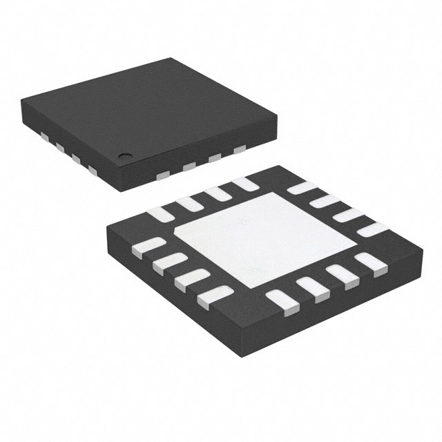


 工商网监
湘ICP备2023018690号
工商网监
湘ICP备2023018690号

