Obsolete Device
Please use SST25VF080B
SST25PF080B
8 Mbit 2.3-3.6V SPI Serial Flash
Features
Product Description
• Single Voltage Read and Write Operations
- 2.3-3.6V
• Serial Interface Architecture
- SPI Compatible: Mode 0 and Mode 3
• High Speed Clock Frequency
- 80 MHz (2.7-3.6V)
- 50 MHz (2.3-2.7V)
• Superior Reliability
- Endurance: 100,000 Cycles (typical)
- Greater than 100 years Data Retention
• Low Power Consumption:
- Active Read Current: 10 mA (typical)
- Standby Current: 5 μA (typical)
• Flexible Erase Capability
- Uniform 4 KByte sectors
- Uniform 32 KByte overlay blocks
- Uniform 64 KByte overlay blocks
• Fast Erase and Byte-Program:
- Chip-Erase Time: 35 ms (typical)
- Sector-/Block-Erase Time: 18 ms (typical)
- Byte-Program Time: 7 μs (typical)
• Auto Address Increment (AAI) Programming
- Decrease total chip programming time over
Byte-Program operations
• End-of-Write Detection
- Software polling the BUSY bit in Status Register
- Busy Status readout on SO pin in AAI Mode
• Hold Pin (HOLD#)
- Suspends a serial sequence to the memory
without deselecting the device
• Write Protection (WP#)
- Enables/Disables the Lock-Down function of the
status register
• Software Write Protection
- Write protection through Block-Protection bits in
status register
• Temperature Range
- Commercial: 0°C to +70°C
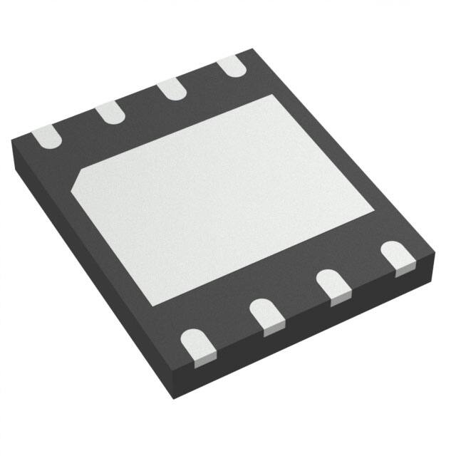
• Packages Available
- 8-lead SOIC (150 mils)
- 8-lead SOIC (200 mils)
- 8-contact WSON (6mm x 5mm)
• All devices are RoHS compliant
The 25 series Serial Flash family features a four-wire,
SPI-compatible interface that allows for a low pin-count
package which occupies less board space and ultimately lowers total system costs. The SST25PF080B
devices are enhanced with improved operating frequency and lower power consumption. SST25PF080B
SPI serial flash memories are manufactured with proprietary, high-performance CMOS SuperFlash technology. The split-gate cell design and thick-oxide tunneling
injector attain better reliability and manufacturability
compared with alternate approaches.
2014 Microchip Technology Inc.
The SST25PF080B devices significantly improve performance and reliability, while lowering power consumption. The devices write (Program or Erase) with a
single power supply of 2.3-3.6V for SST25PF080B.
The total energy consumed is a function of the applied
voltage, current, and time of application. Since for any
given voltage range, the SuperFlash technology uses
less current to program and has a shorter erase time,
the total energy consumed during any Erase or Program operation is less than alternative flash memory
technologies.
The SST25PF080B device is offered in 8-lead SOIC
(150 mils), 8-lead SOIC (200 mils), and 8-contact
WSON (6mm x 5mm). See Figure 2-1 for pin assignments.
DS20005137B-page 1
�SST25PF080B
1.0
BLOCK DIAGRAM
SuperFlash
Memory
X - Decoder
Address
Buffers
and
Latches
Y - Decoder
I/O Buffers
and
Data Latches
Control Logic
Serial Interface
25137 B1.0
CE#
FIGURE 1-1:
DS20005137B-page 2
SCK
SI
SO
WP#
HOLD#
FUNCTIONAL BLOCK DIAGRAM
2014 Microchip Technology Inc.
�SST25PF080B
2.0
PIN DESCRIPTION
CE#
1
SO
2
8
VDD
7
HOLD#
CE#
1
SO
2
Top View
8
VDD
7
HOLD#
Top View
WP#
3
6
SCK
WP#
3
6
SCK
VSS
4
5
SI
VSS
4
5
SI
25137 08-soic S2A P1.0
8-lead SOIC
FIGURE 2-1:
TABLE 2-1:
25137 08-wson A P2.0
8-contact WSON
PIN ASSIGNMENTS
PIN DESCRIPTION
Symbol
Pin Name
Functions
SCK
Serial Clock
To provide the timing of the serial interface.
Commands, addresses, or input data are latched on the rising edge of the clock
input, while output data is shifted out on the falling edge of the clock input.
SI
Serial Data Input
To transfer commands, addresses, or data serially into the device.
Inputs are latched on the rising edge of the serial clock.
SO
Serial Data Output
To transfer data serially out of the device.
Data is shifted out on the falling edge of the serial clock.
Outputs Flash busy status during AAI Programming when reconfigured as RY/BY#
pin. See “Hardware End-of-Write Detection” on page 9 for details.
CE#
Chip Enable
The device is enabled by a high to low transition on CE#. CE# must remain low for
the duration of any command sequence.
WP#
Write Protect
The Write Protect (WP#) pin is used to enable/disable BPL bit in the status register.
HOLD#
Hold
To temporarily stop serial communication with SPI flash memory without resetting
the device.
VDD
Power Supply
To provide power supply voltage: 2.3-3.6V for SST25PF080B
VSS
Ground
2014 Microchip Technology Inc.
DS20005137B-page 3
�SST25PF080B
3.0
used to select the device, and data is accessed through
the Serial Data Input (SI), Serial Data Output (SO), and
Serial Clock (SCK).
MEMORY ORGANIZATION
The SST25PF080B SuperFlash memory array is organized in uniform 4 KByte erasable sectors with 32
KByte overlay blocks and 64 KByte overlay erasable
blocks.
4.0
The SST25PF080B supports both Mode 0 (0,0) and
Mode 3 (1,1) of SPI bus operations. The difference
between the two modes, as shown in Figure 4-1, is the
state of the SCK signal when the bus master is in
Standby mode and no data is being transferred. The
SCK signal is low for Mode 0 and SCK signal is high for
Mode 3. For both modes, the Serial Data In (SI) is sampled at the rising edge of the SCK clock signal and the
Serial Data Output (SO) is driven after the falling edge
of the SCK clock signal.
DEVICE OPERATION
The SST25PF080B is accessed through the SPI (Serial
Peripheral Interface) bus compatible protocol. The SPI
bus consist of four control lines; Chip Enable (CE#) is
CE#
SCK
MODE 3
MODE 3
MODE 0
MODE 0
Bit 7 Bit 6 Bit 5 Bit 4 Bit 3 Bit 2 Bit 1 Bit 0
SI
MSB
HIGH IMPEDANCE
DON T CARE
Bit 7 Bit 6 Bit 5 Bit 4 Bit 3 Bit 2 Bit 1 Bit 0
SO
MSB
FIGURE 4-1:
4.1
25137 SPIprot.0
SPI PROTOCOL
Hold Operation
The HOLD# pin is used to pause a serial sequence
underway with the SPI flash memory without resetting
the clocking sequence. To activate the HOLD# mode,
CE# must be in active low state. The HOLD# mode
begins when the SCK active low state coincides with
the falling edge of the HOLD# signal. The HOLD mode
ends when the HOLD# signal’s rising edge coincides
with the SCK active low state.
If the falling edge of the HOLD# signal does not coincide with the SCK active low state, then the device
enters Hold mode when the SCK next reaches the
active low state. Similarly, if the rising edge of the
HOLD# signal does not coincide with the SCK active
low state, then the device exits in Hold mode when the
SCK next reaches the active low state. See Figure 4-2
for Hold Condition waveform.
Once the device enters Hold mode, SO will be in highimpedance state while SI and SCK can be VIL or VIH.
If CE# is driven active high during a Hold condition, the
device returns to Standby mode. As long as HOLD#
signal is low, the memory remains in the Hold condition.
To resume communication with the device, HOLD#
must be driven active high, and CE# must be driven
active low. See Figure 5-3 for Hold timing.
SCK
HOLD#
Active
Hold
Active
Hold
Active
25137 HoldCond.0
FIGURE 4-2:
DS20005137B-page 4
HOLD CONDITION WAVEFORM
2014 Microchip Technology Inc.
�SST25PF080B
4.2
4.2.1
Write Protection
The Write Protect (WP#) pin enables the lock-down
function of the BPL bit (bit 7) in the status register.
When WP# is driven low, the execution of the WriteStatus-Register (WRSR) instruction is determined by
the value of the BPL bit (see Table 4-1). When WP# is
high, the lock-down function of the BPL bit is disabled.
SST25PF080B provides software Write protection. The
Write Protect pin (WP#) enables or disables the lockdown function of the status register. The Block-Protection bits (BP2, BP1, BP0, and BPL) in the status register provide Write protection to the memory array and
the status register. See Table 4-3 for the Block-Protection description.
TABLE 4-1:
4.3
CONDITIONS TO EXECUTE WRITE-STATUS-REGISTER (WRSR) INSTRUCTION
WP#
BPL
L
1
Not Allowed
L
0
Allowed
H
X
Allowed
Execute WRSR Instruction
Security ID
SST25PF080B offers a 256-bit Security ID (Sec ID)
feature. The Security ID space is divided into two parts
– one factory-programmed, 64-bit segment and one
user-programmable 192-bit segment. The factory-programmed segment is programmed at Microchip with a
unique number and cannot be changed. The user-programmable segment is left unprogrammed for the customer to program as desired.
Use the Program SID command to program the Security ID using the address shown in Table 4-5. Once programmed, the Security ID can be locked using the
Lockout SID command. This prevents any future write
to the Security ID.
TABLE 4-2:
WRITE PROTECT PIN (WP#)
The factory-programmed portion of the Security ID can
never be programmed, and none of the Security ID can
be erased.
4.4
Status Register
The software status register provides status on
whether the flash memory array is available for any
Read or Write operation, whether the device is Write
enabled, and the state of the Memory Write protection.
During an internal Erase or Program operation, the status register may be read only to determine the completion of an operation in progress. Table 4-2 describes
the function of each bit in the software status register.
SOFTWARE STATUS REGISTER
Default at
Power-up
Read/Write
1 = Internal Write operation is in progress
0 = No internal Write operation is in progress
0
R
WEL
1 = Device is memory Write enabled
0 = Device is not memory Write enabled
0
R
2
BP0
Indicates current level of block write protection
1
R/W
3
BP1
Indicates current level of block write protection
1
R/W
4
BP2
Indicates current level of block write protection
5
SEC1
Security ID status
1 = Security ID space locked
0 = Security ID space not locked
6
AAI
7
BPL
Bit
Name
Function
0
BUSY
1
1
R/W
0 or 1
R
Auto Address Increment Programming status
1 = AII programming mode
0 = Byte-Program mode
0
R
1 = BP2, BP1, BP0 are read-only bits
0 = BP2, BP1, BP0 are readable/writable
0
R/W
1. The Security ID status will always be ‘1’ at power-up after a successful execution of the Lockout SID instruction; otherwise,
the default at power-up is ‘0’.
2014 Microchip Technology Inc.
DS20005137B-page 5
�SST25PF080B
4.4.1
BUSY
4.4.3
The Busy bit determines whether there is an internal
Erase or Program operation in progress. A “1” for the
Busy bit indicates the device is busy with an operation
in progress. A “0” indicates the device is ready for the
next valid operation.
4.4.2
The Auto Address Increment Programming-Status bit
provides status on whether the device is in AAI programming mode or Byte-Program mode. The default at
power up is Byte-Program mode.
4.4.4
WRITE ENABLE LATCH (WEL)
•
•
•
•
•
•
4.4.5
BLOCK PROTECTION (BP2, BP1,
BP0)
The Block-Protection (BP2, BP1, BP0) bits define the
size of the memory area, as defined in Table 4-3, to be
software protected against any memory Write (Program or Erase) operation. The Write-Status-Register
(WRSR) instruction is used to program the BP2, BP1
and BP0 bits as long as WP# is high or the Block-Protect-Lock (BPL) bit is 0. Chip-Erase can only be executed if Block-Protection bits are all 0. After power-up,
BP2, BP1 and BP0 are set to 1.
Power-up
Write-Disable (WRDI) instruction completion
Byte-Program instruction completion
Auto Address Increment (AAI) programming is
completed or reached its highest unprotected
memory address
Sector-Erase instruction completion
Block-Erase instruction completion
Chip-Erase instruction completion
Write-Status-Register instruction completion
Program SID instruction completion
Lockout SID instruction completion
TABLE 4-3:
SECURITY ID STATUS (SEC)
The Security ID Status (SEC) bit indicates when the
Security ID space is locked to prevent a Write command. The SEC is ‘1’ after the host issues a Lockout
SID command. Once the host issues a Lockout SID
command, the SEC can never be reset to ‘0’.
The Write-Enable-Latch bit indicates the status of the
internal memory Write Enable Latch. If the WriteEnable-Latch bit is set to “1”, it indicates the device is
Write enabled. If the bit is set to “0” (reset), it indicates
the device is not Write enabled and does not accept
any memory Write (Program/Erase) commands. The
Write-Enable-Latch bit is automatically reset under the
following conditions:
•
•
•
•
AUTO ADDRESS INCREMENT (AAI)
4.4.6
BLOCK PROTECTION LOCK-DOWN
(BPL)
WP# pin driven low (VIL), enables the Block-ProtectionLock-Down (BPL) bit. When BPL is set to 1, it prevents
any further alteration of the BPL, BP2, BP1, and BP0
bits. When the WP# pin is driven high (VIH), the BPL bit
has no effect and its value is “Don’t Care”. After powerup, the BPL bit is reset to 0.
SOFTWARE STATUS REGISTER BLOCK PROTECTION FOR SST25PF080B1
Status Register Bit2
Protection Level
Protected Memory Address
BP2
BP1
BP0
8 Mbit
None
0
0
0
None
Upper 1/16
0
0
1
F0000H-FFFFFH
Upper 1/8
0
1
0
E0000H-FFFFFH
Upper 1/4
0
1
1
C0000H-FFFFFH
Upper 1/2
1
0
0
80000H-FFFFFH
All Blocks
1
0
1
00000H-FFFFFH
All Blocks
1
1
0
00000H-FFFFFH
All Blocks
1
1
1
00000H-FFFFFH
1. X = Don’t Care (RESERVED) default is ‘0’
2. Default at power-up for BP2, BP1, and BP0 is ‘111’. (All Blocks Protected)
DS20005137B-page 6
2014 Microchip Technology Inc.
�SST25PF080B
4.5
Instructions
SCK starting with the most significant bit. CE# must be
driven low before an instruction is entered and must be
driven high after the last bit of the instruction has been
shifted in (except for Read, Read-ID, and Read-StatusRegister instructions). Any low to high transition on
CE#, before receiving the last bit of an instruction bus
cycle, will terminate the instruction in progress and
return the device to standby mode. Instruction commands (Op Code), addresses, and data are all input
from the most significant bit (MSB) first.
Instructions are used to read, write (Erase and Program), and configure the SST25PF080B. The instruction bus cycles are 8 bits each for commands (Op
Code), data, and addresses. Prior to executing any
Byte-Program, Auto Address Increment (AAI) programming, Sector-Erase, Block-Erase, Write-Status-Register, or Chip-Erase instructions, the Write-Enable
(WREN) instruction must be executed first. The complete list of instructions is provided in Table 4-4. All
instructions are synchronized off a high to low transition
of CE#. Inputs will be accepted on the rising edge of
TABLE 4-4:
DEVICE OPERATION INSTRUCTIONS
Instruction
Description
Op Code Cycle1
Address
Cycle(s)2
Dummy
Cycle(s)
Data
Cycle(s)
Read
Read Memory
0000 0011b (03H)
3
0
1 to
High-Speed Read
Read Memory at higher speed
0000 1011b (0BH)
3
1
1 to
4 KByte Sector-Erase3
Erase 4 KByte of
memory array
0010 0000b (20H)
3
0
0
32 KByte Block-Erase4
Erase 32 KByte block
of memory array
0101 0010b (52H)
3
0
0
64 KByte Block-Erase5
Erase 64 KByte block
of memory array
1101 1000b (D8H)
3
0
0
Chip-Erase
Erase Full Memory Array
0110 0000b (60H) or
1100 0111b (C7H)
0
0
0
To Program One Data Byte
0000 0010b (02H)
3
0
1
AAI-Word-Program
Auto Address Increment
Programming
1010 1101b (ADH)
3
0
2 to
RDSR7
Read-Status-Register
0000 0101b (05H)
0
0
1 to
EWSR
Enable-Write-Status-Register
0101b 0000b (50H)
0
0
0
WRSR
Write-Status-Register
0000 0001b (01H)
0
0
1
WREN
Write-Enable
0000 0110b (06H)
0
0
0
WRDI
Write-Disable
0000 0100b (04H)
0
0
0
RDID
Read-ID
1001 0000b (90H) or
1010 1011b (ABH)
3
0
1 to
Byte-Program
6
8
JEDEC-ID
JEDEC ID Read
1001 1111b (9FH)
0
0
3 to
EBSY
Enable SO to output RY/BY#
status during AAI programming
0111 0000b (70H)
0
0
0
DBSY
Disable SO to output RY/BY#
status during AAI programming
1000 0000b (80H)
0
0
0
Read SID
Read Security ID
1000 1000b (88H)
1
1
1 to 32
Program SID9
Program User Security ID area
1010 0101b (A5H)
1
0
1
Lockout Security ID Programming 1000 0101b (85H)
0
0
0
9
Lockout SID
1.
2.
3.
4.
5.
6.
One bus cycle is eight clock periods.
Address bits above the most significant bit of each density can be VIL or VIH.
4KByte Sector Erase addresses: use AMS-A12, remaining addresses are don’t care but must be set either at VIL or VIH.
32KByte Block Erase addresses: use AMS-A15, remaining addresses are don’t care but must be set either at VIL or VIH.
64KByte Block Erase addresses: use AMS-A16, remaining addresses are don’t care but must be set either at VIL or VIH.
To continue programming to the next sequential address location, enter the 8-bit command, ADH, followed by 2 bytes of data
to be programmed. Data Byte 0 will be programmed into the initial address [A23-A1] with A0=0, Data Byte 1 will be programmed into the initial address [A23-A1] with A0=1.
7. The Read-Status-Register is continuous with ongoing clock cycles until terminated by a low to high transition on CE#.
2014 Microchip Technology Inc.
DS20005137B-page 7
�SST25PF080B
8. Manufacturer’s ID is read with A0=0, and Device ID is read with A0=1. All other address bits are 00H. The Manufacturer’s ID
and Device ID output stream is continuous until terminated by a low-to-high transition on CE#.
9. Requires a prior WREN command.
4.5.1
READ (33/25 MHZ)
is reached, the address pointer will automatically increment to the beginning (wrap-around) of the address
space. Once the data from address location 1FFFFFH
has been read, the next output will be from address
location 000000H.
The Read instruction, 03H, supports up to 33 MHz (2.73.6V operation) or 25 MHz (2.3-2.7V operation) Read.
The device outputs the data starting from the specified
address location. The data output stream is continuous
through all addresses until terminated by a low to high
transition on CE#. The internal address pointer will
automatically increment until the highest memory
address is reached. Once the highest memory address
The Read instruction is initiated by executing an 8-bit
command, 03H, followed by address bits [A23-A0].
CE# must remain active low for the duration of the
Read cycle. See Figure 4-3 for the Read sequence.
CE#
MODE 3
SCK
0 1 2 3 4 5 6 7 8
23 24
15 16
31 32
39 40
47
48
55 56
63 64
70
MODE 0
03
SI
ADD.
ADD.
ADD.
MSB
MSB
N
DOUT
HIGH IMPEDANCE
SO
N+1
DOUT
N+2
DOUT
N+3
DOUT
N+4
DOUT
MSB
25137 ReadSeq 0.0
FIGURE 4-3:
4.5.2
READ SEQUENCE
HIGH-SPEED-READ (80/50 MHZ)
through all addresses until terminated by a low to high
transition on CE#. The internal address pointer will
automatically increment until the highest memory
address is reached. Once the highest memory address
is reached, the address pointer will automatically increment to the beginning (wrap-around) of the address
space. Once the data from address location FFFFFH
has been read, the next output will be from address
location 00000H.
The High-Speed-Read instruction supporting up to 80
MHz (2.7-3.6V operation) or 50 MHz (2.3-2.7V operation) Read is initiated by executing an 8-bit command,
0BH, followed by address bits [A23-A0] and a dummy
byte. CE# must remain active low for the duration of the
High-Speed-Read cycle. See Figure 4-4 for the HighSpeed-Read sequence.
Following a dummy cycle, the High-Speed-Read
instruction outputs the data starting from the specified
address location. The data output stream is continuous
CE#
MODE 3
SCK
0 1 2 3 4 5 6 7 8
15 16
23 24
31 32
39 40
47 48
55 56
63 64
71 72
80
MODE 0
0B
SI
MSB
ADD.
MSB
ADD.
ADD.
HIGH IMPEDANCE
SO
X
N
DOUT
N+1
DOUT
N+2
DOUT
N+3
DOUT
N+4
DOUT
MSB
Note: X = Dummy Byte: 8 Clocks Input Dummy Cycle (VIL or VIH)
FIGURE 4-4:
DS20005137B-page 8
25137 HSRdSeq.0
HIGH-SPEED-READ SEQUENCE
2014 Microchip Technology Inc.
�SST25PF080B
4.5.3
BYTE-PROGRAM
The Byte-Program instruction is initiated by executing
an 8-bit command, 02H, followed by address bits [A23A0]. Following the address, the data is input in order
from MSB (bit 7) to LSB (bit 0). CE# must be driven
high before the instruction is executed. The user may
poll the Busy bit in the software status register or wait
TBP for the completion of the internal self-timed ByteProgram operation. See Figure 4-5 for the Byte-Program sequence.
The Byte-Program instruction programs the bits in the
selected byte to the desired data. The selected byte
must be in the erased state (FFH) when initiating a Program operation. A Byte-Program instruction applied to a
protected memory area will be ignored.
Prior to any Write operation, the Write-Enable (WREN)
instruction must be executed. CE# must remain active
low for the duration of the Byte-Program instruction.
CE#
MODE 3
SCK
0 1 2 3 4 5 6 7 8
15 16
23 24
31 32
39
MODE 0
ADD.
02
SI
SO
ADD.
MSB
MSB
ADD.
DIN
MSB LSB
HIGH IMPEDANCE
25137 ByteProg.0
FIGURE 4-5:
4.5.4
BYTE-PROGRAM SEQUENCE
AUTO ADDRESS INCREMENT (AAI)
WORD-PROGRAM
The AAI program instruction allows multiple bytes of
data to be programmed without re-issuing the next
sequential address location. This feature decreases
total programming time when multiple bytes or entire
memory array is to be programmed. An AAI Word program instruction pointing to a protected memory area
will be ignored. The selected address range must be in
the erased state (FFH) when initiating an AAI Word
Program operation. While within AAI Word Programming sequence, only the following instructions are
valid: for software end-of-write detection—AAI Word
(ADH), WRDI (04H), and RDSR (05H); for hardware
end-of-write detection—AAI Word (ADH) and WRDI
(04H). There are three options to determine the completion of each AAI Word program cycle: hardware
detection by reading the Serial Output, software detection by polling the BUSY bit in the software status register, or wait TBP. Refer to“End-of-Write Detection” for
details.
Prior to any write operation, the Write-Enable (WREN)
instruction must be executed. Initiate the AAI Word
Program instruction by executing an 8-bit command,
ADH, followed by address bits [A23-A0]. Following the
addresses, two bytes of data are input sequentially,
each one from MSB (Bit 7) to LSB (Bit 0). The first byte
of data (D0) is programmed into the initial address [A23A1] with A0=0, the second byte of Data (D1) is programmed into the initial address [A23-A1] with A0=1.
CE# must be driven high before executing the AAI
Word Program instruction. Check the BUSY status
before entering the next valid command. Once the
2014 Microchip Technology Inc.
device indicates it is no longer busy, data for the next
two sequential addresses may be programmed, followed by the next two, and so on.
When programming the last desired word, or the highest unprotected memory address, check the busy status using either the hardware or software (RDSR
instruction) method to check for program completion.
Once programming is complete, use the applicable
method to terminate AAI. If the device is in Software
End-of-Write Detection mode, execute the Write-Disable (WRDI) instruction, 04H. If the device is in AAI
Hardware End-of-Write Detection mode, execute the
Write-Disable (WRDI) instruction, 04H, followed by the
8-bit DBSY command, 80H. There is no wrap mode
during AAI programming once the highest unprotected
memory address is reached. See Figures 4-8 and 4-9
for the AAI Word programming sequence.
4.5.5
END-OF-WRITE DETECTION
There are three methods to determine completion of a
program cycle during AAI Word programming: hardware detection by reading the Serial Output, software
detection by polling the BUSY bit in the Software Status
Register, or wait TBP. The Hardware End-of-Write
detection method is described in the section below.
4.5.6
HARDWARE END-OF-WRITE
DETECTION
The Hardware End-of-Write detection method eliminates the overhead of polling the Busy bit in the Software Status Register during an AAI Word program
operation. The 8-bit command, 70H, configures the
Serial Output (SO) pin to indicate Flash Busy status
during AAI Word programming. (see Figure 4-6) The 8-
DS20005137B-page 9
�SST25PF080B
While in AAI and Hardware End-of-Write detection
mode, the only valid instructions are AAI Word (ADH)
and WRDI (04H).
bit command, 70H, must be executed prior to initiating
an AAI Word-Program instruction. Once an internal
programming operation begins, asserting CE# will
immediately drive the status of the internal flash status
on the SO pin. A ‘0’ indicates the device is busy and a
‘1’ indicates the device is ready for the next instruction.
De-asserting CE# will return the SO pin to tri-state.
To exit AAI Hardware End-of-Write detection, first execute WRDI instruction, 04H, to reset the Write-EnableLatch bit (WEL=0) and AAI bit. Then execute the 8-bit
DBSY command, 80H, to disable RY/BY# status during
the AAI command. See Figures 4-7 and 4-8.
CE#
MODE 3
SCK
0 1 2 3 4 5 6 7
MODE 0
70
SI
MSB
SO
HIGH IMPEDANCE
25137 EnableSO.0
FIGURE 4-6:
ENABLE SO AS HARDWARE RY/BY# DURING AAI PROGRAMMING
CE#
MODE 3
SCK
0 1 2 3 4 5 6 7
MODE 0
80
SI
MSB
SO
HIGH IMPEDANCE
25137 DisableSO.0
FIGURE 4-7:
DS20005137B-page 10
DISABLE SO AS HARDWARE RY/BY# DURING AAI PROGRAMMING
2014 Microchip Technology Inc.
�SST25PF080B
CE#
MODE 3
0
7
0
0
7
7 8
15 16 23 24
31 32 39 40 47
0
7 8
15 16 23
SCK MODE 0
SI
AD
WREN
EBSY
A
A
A
D0
D1
AD
D2
D3
Load AAI command, Address, 2 bytes data
SO
Check for Flash Busy Status to load next valid1 command
CE# cont.
0
7 8
15 16 23
0
7
0
7
0
7 8
15
SCK cont.
Dn-1
AD
SI cont.
WRDI
Dn
Last 2
Data Bytes
RDSR
DBSY
WRDI followed by DBSY
to exit AAI Mode
DOUT
SO cont.
1
Check for Flash Busy Status to load next valid command
Note:
1. Valid commands during AAI programming: AAI command or WRDI command
2. User must configure the SO pin to output Flash Busy status during AAI programming
25137 AAI.HW.3
FIGURE 4-8:
AUTO ADDRESS INCREMENT (AAI) WORD-PROGRAM SEQUENCE WITH
HARDWARE END-OF-WRITE DETECTION
Wait TBP or poll Software Status
register to load next valid1 command
CE#
MODE 3
0
7 8
15 16 23 24
31 32 39 40 47
0
7 8
15 16 23
0
7 8
15 16 23
0
7
0
7 8
15
SCK MODE 0
SI
AD
A
A
A
D0
D1
Load AAI command, Address, 2 bytes data
AD
D2
D3
AD
Dn-1
Dn
Last 2
Data Bytes
SO
Note:
WRDI
RDSR
WRDI to exit
AAI Mode
DOUT
1. Valid commands during AAI programming: AAI command, RDSR command, or WRDI command
FIGURE 4-9:
25137 AAI.SW.3
AUTO ADDRESS INCREMENT (AAI) WORD-PROGRAM SEQUENCE WITH
SOFTWARE END-OF-WRITE DETECTION
2014 Microchip Technology Inc.
DS20005137B-page 11
�SST25PF080B
4.5.7
4-KBYTE SECTOR-ERASE
The Sector-Erase instruction clears all bits in the
selected 4 KByte sector to FFH. A Sector-Erase
instruction applied to a protected memory area will be
ignored. Prior to any Write operation, the Write-Enable
(WREN) instruction must be executed. CE# must
remain active low for the duration of any command
sequence. The Sector-Erase instruction is initiated by
executing an 8-bit command, 20H, followed by address
bits [A23-A0]. Address bits [AMS-A12] (AMS = Most Significant address) are used to determine the sector
address (SAX), remaining address bits can be VIL or VIH.
CE# must be driven high before the instruction is executed. The user may poll the Busy bit in the software
status register or wait TSE for the completion of the
internal self-timed Sector-Erase cycle. See Figure 4-10
for the Sector-Erase sequence.
CE#
MODE 3
SCK
0 1 2 3 4 5 6 7 8
15 16
23 24
31
MODE 0
ADD.
ADD.
20
SI
MSB
ADD.
MSB
SO
HIGH IMPEDANCE
25137 SecErase.0
FIGURE 4-10:
4.5.8
SECTOR-ERASE SEQUENCE
32-KBYTE AND 64-KBYTE BLOCKERASE
The 32-KByte Block-Erase instruction clears all bits in
the selected 32 KByte block to FFH. A Block-Erase
instruction applied to a protected memory area will be
ignored. The 64-KByte Block-Erase instruction clears all bits
in the selected 64 KByte block to FFH. A Block-Erase
instruction applied to a protected memory area will be
ignored. Prior to any Write operation, the Write-Enable
(WREN) instruction must be executed. CE# must remain
active low for the duration of any command sequence.
The 32-KByte Block-Erase instruction is initiated by
executing an 8-bit command, 52H, followed by address
bits [A23-A0]. Address bits [AMS-A15] (AMS = Most Sig-
nificant Address) are used to determine block address
(BAX), remaining address bits can be VIL or VIH. CE#
must be driven high before the instruction is executed. The
64-KByte Block-Erase instruction is initiated by executing an
8-bit command D8H, followed by address bits [A23-A0].
Address bits [AMS-A16] are used to determine block address
(BAX), remaining address bits can be VIL or VIH. CE# must
be driven high before the instruction is executed. The user
may poll the Busy bit in the software status register or wait
TBE for the completion of the internal self-timed 32KByte Block-Erase or 64-KByte Block-Erase cycles.
See Figures 4-11 and 4-12 for the 32-KByte BlockErase and 64-KByte Block-Erase sequences.
CE#
MODE 3
SCK
0 1 2 3 4 5 6 7 8
52
SI
MSB
SO
15 16
23 24
31
MODE 0
ADDR
ADDR
ADDR
MSB
HIGH IMPEDANCE
25137 32KBklEr.0
FIGURE 4-11:
DS20005137B-page 12
32-KBYTE BLOCK-ERASE SEQUENCE
2014 Microchip Technology Inc.
�SST25PF080B
CE#
MODE 3
SCK
0 1 2 3 4 5 6 7 8
23 24
15 16
31
MODE 0
ADDR
ADDR
D8
SI
MSB
ADDR
MSB
SO
HIGH IMPEDANCE
25137 63KBlkEr.0
FIGURE 4-12:
4.5.9
64-KBYTE BLOCK-ERASE SEQUENCE
CHIP-ERASE
The Chip-Erase instruction clears all bits in the device
to FFH. A Chip-Erase instruction will be ignored if any
of the memory area is protected. Prior to any Write operation, the Write-Enable (WREN) instruction must be executed. CE# must remain active low for the duration of
the Chip-Erase instruction sequence. The Chip-Erase
instruction is initiated by executing an 8-bit command,
60H or C7H. CE# must be driven high before the instruction
is executed. The user may poll the Busy bit in the software
status register or wait TCE for the completion of the
internal self-timed Chip-Erase cycle. See Figure 4-13
for the Chip-Erase sequence.
CE#
MODE 3
SCK
0 1 2 3 4 5 6 7
MODE 0
60 or C7
SI
MSB
SO
HIGH IMPEDANCE
25137 ChEr.0
FIGURE 4-13:
4.6
CHIP-ERASE SEQUENCE
Read Security ID
To execute a Read SID operation, the host drives CE#
low, sends the Read Security ID command cycle (88H),
one address cycle, and then one dummy cycle. Each
cycle is eight clock periods long, most significant bit
first.
After the dummy cycle, the device outputs data on the
falling edge of the SCK signal starting from the specified address location. The data output stream is continuous through all SID addresses until terminated by a
low-to-high transition on CE#. The internal address
pointer automatically increments until the last SID
address is reached, then outputs 00H until CE# goes
high.
2014 Microchip Technology Inc.
4.7
Lockout Security ID
The Lockout SID instruction prevents any future
changes to the Security ID. To execute a Lockout SID,
the host drives CE# low, sends the Lockout SID command cycle (85H), then drives CE# high. Each cycle is
eight clocks long, most significant bit first. Poll the
BUSY bit in the software status register, or wait TPSID,
for the completion of the Lockout SID operation.
DS20005137B-page 13
�SST25PF080B
4.8
Program Security ID
To execute a Program SID operation, the host drives
CE# low, sends the Program SID command cycle
(A5H), one address cycle, the data to be programmed,
then drives CE# high. Each cycle is eight clocks long,
most significant bit first. To determine the completion of
the internal, self-timed Program SID operation, poll the
BUSY bit in the software status register, or wait TPSID
for the completion of the internal self-timed Program
SID operation.
The Program SID instruction programs a byte of data in
the user-programmable, Security ID space. Security ID
addresses 08h-1FH are the user-programmable locations. The device ignores a Program Security ID
instruction pointing to an invalid or protected address,
see Table 4-5. Prior to the program operation, execute
WREN.
TABLE 4-5:
PROGRAM SECURITY ID
Program Security ID
Address Range
Pre-Programmed at factory
00H – 07H
User Programmable
08H – 1FH
4.8.1
READ-STATUS-REGISTER (RDSR)
properly received by the device. CE# must be driven
low before the RDSR instruction is entered and remain
low until the status data is read. Read-Status-Register
is continuous with ongoing clock cycles until it is terminated by a low to high transition of the CE#. See Figure
4-14 for the RDSR instruction sequence.
The Read-Status-Register (RDSR) instruction allows
reading of the status register. The status register may
be read at any time even during a Write (Program/
Erase) operation. When a Write operation is in progress, the Busy bit may be checked before sending any
new commands to assure that the new commands are
CE#
MODE 3
SCK
0
1
2
3
4
5
6
7
8
9
10
11
12
13
14
MODE 0
05
SI
MSB
SO
HIGH IMPEDANCE
Bit 7 Bit 6 Bit 5 Bit 4 Bit 3 Bit 2 Bit 1 Bit 0
MSB
Status
Register Out
25137 RDSRseq.0
FIGURE 4-14:
DS20005137B-page 14
READ-STATUS-REGISTER (RDSR) SEQUENCE
2014 Microchip Technology Inc.
�SST25PF080B
4.8.2
WRITE-ENABLE (WREN)
execution of the Write-Status-Register (WRSR)
instruction; however, the Write-Enable-Latch bit in the
Status Register will be cleared upon the rising edge
CE# of the WRSR instruction. CE# must be driven high
before the WREN instruction is executed.
The Write-Enable (WREN) instruction sets the WriteEnable-Latch bit in the Status Register to 1 allowing
Write operations to occur. The WREN instruction must
be executed prior to any Write (Program/Erase) operation. The WREN instruction may also be used to allow
CE#
MODE 3
SCK
0 1 2 3 4 5 6 7
MODE 0
06
SI
MSB
SO
HIGH IMPEDANCE
25137 WREN.0
FIGURE 4-15:
4.8.3
WRITE ENABLE (WREN) SEQUENCE
WRITE-DISABLE (WRDI)
ress. Any program operation in progress may continue
up to TBP after executing the WRDI instruction. CE#
must be driven high before the WRDI instruction is executed.
The Write-Disable (WRDI) instruction resets the WriteEnable-Latch bit and AAI bit to 0 disabling any new
Write operations from occurring. The WRDI instruction
will not terminate any programming operation in prog-
CE#
MODE 3
SCK
0 1 2 3 4 5 6 7
MODE 0
04
SI
MSB
SO
HIGH IMPEDANCE
25137 WRDI.0
FIGURE 4-16:
4.8.4
WRITE DISABLE (WRDI) SEQUENCE
ENABLE-WRITE-STATUSREGISTER (EWSR)
The Enable-Write-Status-Register (EWSR) instruction
arms the Write-Status-Register (WRSR) instruction
and opens the status register for alteration. The WriteStatus-Register instruction must be executed immediately after the execution of the Enable-Write-StatusRegister instruction. This two-step instruction
sequence of the EWSR instruction followed by the
WRSR instruction works like SDP (software data protection) command structure which prevents any accidental alteration of the status register values. CE# must
2014 Microchip Technology Inc.
be driven low before the EWSR instruction is entered
and must be driven high before the EWSR instruction
is executed.
DS20005137B-page 15
�SST25PF080B
4.8.5
WRITE-STATUS-REGISTER (WRSR)
The Write-Status-Register instruction writes new values to the BP2, BP1, BP0, and BPL bits of the status
register. CE# must be driven low before the command
sequence of the WRSR instruction is entered and
driven high before the WRSR instruction is executed.
See Figure 4-17 for EWSR or WREN and WRSR
instruction sequences.
Executing the Write-Status-Register instruction will be
ignored when WP# is low and BPL bit is set to “1”.
When the WP# is low, the BPL bit can only be set from
“0” to “1” to lock-down the status register, but cannot be
reset from “1” to “0”. When WP# is high, the lock-down
function of the BPL bit is disabled and the BPL, BP0,
BP1, and BP2 bits in the status register can all be
changed. As long as BPL bit is set to 0 or WP# pin is
driven high (VIH) prior to the low-to-high transition of the
CE# pin at the end of the WRSR instruction, the bits in
the status register can all be altered by the WRSR
instruction. In this case, a single WRSR instruction can
set the BPL bit to “1” to lock down the status register as
well as altering the BP0, BP1, and BP2 bits at the same
time. See Table 4-1 for a summary description of WP#
and BPL functions.
CE#
MODE 3
SCK
0 1 2 3 4 5 6 7
MODE 0
0 1 2 3 4 5 6 7 8 9 10 11 12 13 14 15
MODE 0
01
50 or 06
SI
MSB
SO
MODE 3
MSB
STATUS
REGISTER IN
7 6 5 4 3 2 1 0
MSB
HIGH IMPEDANCE
25137 EWSR.0
FIGURE 4-17:
DS20005137B-page 16
ENABLE-WRITE-STATUS-REGISTER (EWSR) OR WRITE-ENABLE (WREN) AND
WRITE-STATUS-REGISTER (WRSR) SEQUENCE
2014 Microchip Technology Inc.
�SST25PF080B
4.8.6
JEDEC READ-ID
out on the SO pin. Byte 1, BFH, identifies the manufacturer as Microchip. Byte 2, 25H, identifies the memory
type as SPI Serial Flash. Byte 3, 8EH, identifies the
device as SST25PF080B. The instruction sequence is
shown in Figure 4-18. The JEDEC Read ID instruction
is terminated by a low to high transition on CE# at any
time during data output.
The JEDEC Read-ID instruction identifies the device as
SST25PF080B and the manufacturer as Microchip.
The device information can be read from executing the
8-bit command, 9FH. Following the JEDEC Read-ID
instruction, the 8-bit manufacturer’s ID, BFH, is output
from the device. After that, a 16-bit device ID is shifted
CE#
MODE 3
SCK
0 1 2 3 4 5 6 7 8 9 10 11 12 13 14 15 16 17 18 19 20 21 22 23 24 25 26 27 28 29 30 31 32 33 34
MODE 0
SI
9F
HIGH IMPEDANCE
SO
25
BF
MSB
FIGURE 4-18:
TABLE 4-6:
8E
MSB
25137 JEDECID.1
JEDEC READ-ID SEQUENCE
JEDEC READ-ID DATA
Manufacturer’s ID
Device ID
Memory Type
Memory Capacity
Byte1
Byte 2
Byte 3
BFH
25H
8EH
2014 Microchip Technology Inc.
DS20005137B-page 17
�SST25PF080B
4.8.7
READ-ID (RDID)
A0]. Following the Read-ID instruction, the manufacturer’s ID is located in address 00000H and the device
ID is located in address 00001H. Once the device is in
Read-ID mode, the manufacturer’s and device ID output data toggles between address 00000H and 00001H
until terminated by a low to high transition on CE#.
The Read-ID instruction (RDID) identifies the devices
as SST25PF080B and manufacturer as Microchip. This
command is backward compatible and should be used
as default device identification when multiple versions
of SPI Serial Flash devices are used in a design. The
device information can be read from executing an 8-bit
command, 90H or ABH, followed by address bits [A23-
Refer to Tables 4-6 and 4-7 for device identification
data.
CE#
MODE 3
SCK
0 1 2 3 4 5 6 7 8
23 24
15 16
31 32
39 40
47 48
55 56
63
MODE 0
90 or AB
SI
00
MSB
00
ADD1
MSB
HIGH IMPEDANCE
SO
BF
Device ID
BF
Device ID
HIGH
IMPEDANCE
MSB
Note: The manufacturer s and device ID output stream is continuous until terminated by a low to high transition on CE#.
Device ID = 8EH for SST25PF080B
1. 00H will output the manfacturer s ID first and 01H will output device ID first before toggling between the two.
25137 RdID.0
FIGURE 4-19:
TABLE 4-7:
READ-ID SEQUENCE
PRODUCT IDENTIFICATION
Manufacturer’s ID
Address
Data
00000H
BFH
00001H
8EH
Device ID
SST25PF080B
DS20005137B-page 18
2014 Microchip Technology Inc.
�SST25PF080B
5.0
ELECTRICAL SPECIFICATIONS
Absolute Maximum Stress Ratings (Applied conditions greater than those listed under “Absolute Maximum Stress Ratings” may cause permanent damage to the device. This is a stress rating only and functional operation of the device at these conditions or conditions greater than those defined in the operational
sections of this data sheet is not implied. Exposure to absolute maximum stress rating conditions may
affect device reliability.)
Temperature Under Bias. . . . . . . . . . . . . . . . . . . . . . . . . . . . . . . . . . . . . . . . . . . . . . . . . . -55°C to +125°C
Storage Temperature . . . . . . . . . . . . . . . . . . . . . . . . . . . . . . . . . . . . . . . . . . . . . . . . . . . . -65°C to +150°C
D. C. Voltage on Any Pin to Ground Potential. . . . . . . . . . . . . . . . . . . . . . . . . . . . . . . . . -0.5V to VDD+0.5V
Transient Voltage (