Obsolete Device
Please contact Microchip Sales for replacement information.
64 Mbit SPI Serial Dual I/O Flash
SST25VF064C
EOL Data Sheet
The SST 25 series Serial Flash family features a four-wire, SPI-compatible interface that allows for a low pin-count package which occupies less board space and
ultimately lowers total system costs. SST25VF064C SPI serial flash memory is
manufactured with SST proprietary, high-performance CMOS SuperFlash technology. The split-gate cell design and thick-oxide tunneling injector attain better
reliability and manufacturability compared with alternate approaches.
Features
• Single Voltage Read and Write Operations
• Page-Program
– 2.7-3.6V
– 256 Bytes per page
– Single and Dual Input support
– Fast Page-Program time in 1.5 ms (typical)
• Serial Interface Architecture
– SPI Compatible: Mode 0 and Mode 3
• End-of-Write Detection
• Dual Input/Output Support
– Software polling the BUSY bit in Status Register
– Fast-Read Dual-Output Instruction
– Fast-Read Dual I/O Instruction
• Write Protection (WP#)
– Enables/Disables the Lock-Down function of the
status register
• High Speed Clock Frequency
– 80 MHz for High-Speed Read (0BH)
– 75 MHz for Fast-Read Dual-Output (3BH)
– 50 MHz for Fast-Read Dual I/O (BBH)
– 33 MHz for Read Instruction (03H)
• Software Write Protection
– Write protection through Block-Protection bits in status
register
• Superior Reliability
• Security ID
– Endurance: 100,000 Cycles (typical)
– Greater than 100 years Data Retention
– One-Time Programmable (OTP) 256 bit, Secure ID
- 64 bit Unique, Factory Pre-Programmed identifier
- 192 bit User-Programmable
• Low Power Consumption
– Active Read Current: 12 mA (typical @ 80 MHz) for single-bit read)
– Active Read Current: 14 mA (typical @ 75MHz) for dualbit read)
– Standby Current: 5 µA (typical)
• Flexible Erase Capability
– Uniform 4 KByte sectors
– Uniform 32 KByte overlay blocks
– Uniform 64 KByte overlay blocks
• Temperature Range
– Commercial = 0°C to +70°C
– Industrial: -40°C to +85°C
• Packages Available
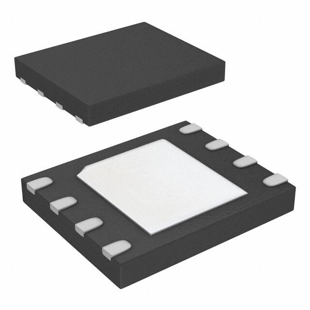
– 16-lead SOIC (300 mils)
– 8-contact WSON (6mm x 8mm)
– 8-lead SOIC (200 mils)
• All devices are RoHS compliant
• Fast Erase
– Chip-Erase Time: 35 ms (typical)
– Sector-/Block-Erase Time: 18 ms (typical)
©2015 Silicon Storage Technology, Inc.
www.microchip.com
DS20005036C
04/15
�64 Mbit SPI Serial Dual I/O Flash
SST25VF064C
EOL Data Sheet
Product Description
The SST 25 series Serial Flash family features a four-wire, SPI-compatible interface that allows for a
low pin-count package which occupies less board space and ultimately lowers total system costs.
SST25VF064C SPI serial flash memory is manufactured with SST proprietary, high-performance
CMOS SuperFlash technology. The split-gate cell design and thick-oxide tunneling injector attain better reliability and manufacturability compared with alternate approaches.
The SST25VF064C significantly improves performance and reliability, while lowering power consumption. The device writes (Program or Erase) with a single power supply of 2.7-3.6V. The total energy
consumed is a function of the applied voltage, current, and time of application. Since for any given voltage range, the SuperFlash technology uses less current to program and has a shorter erase time, the
total energy consumed during any Erase or Program operation is less than alternative flash memory
technologies.
The SST25VF064C device is offered in 16-lead SOIC (300 mils), 8-contact WSON (6mm x 8mm), and
8-lead SOIC (200 mils) packages. See Figure 2 for pin assignments.
©2015 Silicon Storage Technology, Inc.
DS20005036C
2
04/15
�64 Mbit SPI Serial Dual I/O Flash
SST25VF064C
EOL Data Sheet
Block Diagram
SuperFlash
Memory
X - Decoder
Address
Buffers
and
Latches
Y - Decoder
Page Buffer,
I/O Buffers
and
Data Latches
Control Logic
Serial Interface
CE#
SCK
SI/SIO0
SO/SIO1
WP#
RST#/HOLD#
1392 B1.0
Figure 1: Functional Block Diagram
©2015 Silicon Storage Technology, Inc.
DS20005036C
3
04/15
�64 Mbit SPI Serial Dual I/O Flash
SST25VF064C
EOL Data Sheet
Pin Description
RST#/HOLD#
SCK
VDD
SI/SIO0
Top View
NC
NC
NC
NC
NC
NC
NC
NC
CE#
VSS
SO/SIO1
WP#
1392 16-SOIC P1.0
CE#
1
8
SO/SIO1
2
7
WP#
3
6
SCK
VSS
4
5
SI/SIO0
Top View
VDD
RST#/HOLD#
1392 8-WSON P1.0
CE#
1
SO/SIO1
2
WP#
VSS
8
VDD
7
RST#/HOLD#
3
6
SCK
4
5
SI/SIO0
Top View
1392 8-soic S3A P3.1
Figure 2: Pin Assignments for 16-Lead SOIC, 8-Contact WSON, and 8-Lead SOIC
Table 1: Pin Description
Symbol
Pin Name
Functions
SCK
Serial Clock
To provide the timing of the serial interface. Commands, addresses, or input
data are latched on the rising edge of the clock input, while output data is
shifted out on the falling edge of the clock input.
SI
Serial Data Input
To transfer commands, addresses, or data serially into the device.
Inputs are latched on the rising edge of the serial clock.
SO
Serial Data Output To transfer data serially out of the device.
Data is shifted out on the falling edge of the serial clock.
SIO[0:1]
Serial Data Input/
Output for Dual I/
O Mode
To transfer commands, addresses, or data serially into the device, or data
out of the device. Inputs are latched on the rising edge of the serial clock.
Data is shifted out on the falling edge of the serial clock. These pins are for
Dual I/O mode.
CE#
Chip Enable
The device is enabled by a high to low transition on CE#. CE# must remain
low for the duration of any command sequence.
WP#
Write Protect
The Write Protect (WP#) pin is used to enable/disable BPL bit in the status
register.
RST#/HOLD# Reset
To reset the operation of the device and the internal logic. The device powers on with RST# pin functionality as default.
Hold
To temporarily stop serial communication with SPI Flash memory while
device is selected. This is selected by an instruction sequence. See “Reset/
Hold Mode” page 5 for details.
VDD
Power Supply
To provide power supply voltage: 2.7-3.6V
VSS
Ground
T1.0 25036
©2015 Silicon Storage Technology, Inc.
DS20005036C
4
04/15
�64 Mbit SPI Serial Dual I/O Flash
SST25VF064C
EOL Data Sheet
Memory Organization
The SST25VF064C SuperFlash memory array is organized in uniform 4 KByte erasable sectors with
32 KByte overlay blocks and 64 KByte overlay erasable blocks.
Device Operation
The SST25VF064C is accessed through the SPI (Serial Peripheral Interface) bus compatible protocol.
The SPI bus consists of four control lines; Chip Enable (CE#) is used to select the device, and data is
accessed through the Serial Data Input (SI), Serial Data Output (SO), and Serial Clock (SCK).
The SST25VF064C supports both Mode 0 (0,0) and Mode 3 (1,1) of SPI bus operations. The difference
between the two modes, as shown in Figure 3, is the state of the SCK signal when the bus master is in
Stand-by mode and no data is being transferred. The SCK signal is low for Mode 0 and SCK signal is
high for Mode 3. For both modes, the Serial Data In (SI) is sampled at the rising edge of the SCK clock
signal and the Serial Data Output (SO) is driven after the falling edge of the SCK clock signal.
CE#
SCK
SI
MODE 3
MODE 3
MODE 0
MODE 0
Bit 7 Bit 6 Bit 5 Bit 4 Bit 3 Bit 2 Bit 1 Bit 0
MSB
SO
HIGH IMPEDANCE
DON'T CARE
Bit 7 Bit 6 Bit 5 Bit 4 Bit 3 Bit 2 Bit 1 Bit 0
MSB
1392 F04.0
Figure 3: SPI Protocol
Reset/Hold Mode
The RST#/HOLD# pin provides either a hardware reset or a hold pin. From power-on, the RST#/
HOLD# pin defaults as a hardware reset pin (RST#). The Hold mode for this pin is a user selected
option where an EHLD instruction enables the Hold mode. Once selected as a hold pin (HOLD#), the
RST#/HOLD# pin will be configured as a HOLD# pin, and goes back to RST# pin only after a power-off
and power-on sequence.
©2015 Silicon Storage Technology, Inc.
DS20005036C
5
04/15
�64 Mbit SPI Serial Dual I/O Flash
SST25VF064C
EOL Data Sheet
Reset
If the RST#/HOLD# pin is used as a reset pin, RST# pin provides a hardware method for resetting the
device. Driving the RST# pin high puts the device in normal operating mode. The RST# pin must be
driven low for a minimum of TRST time to reset the device. The SO pin is in high impedance state while
the device is in reset. A successful reset will reset the status register to its power-up state (BPL, BUSY
and WEL = 0; BP3, BP2, BP1, and BP0 = 1). See Table 2 for default power-up modes. A device reset
during an active Program or Erase operation aborts the operation and data of the targeted address
range may be corrupted or lost due to the aborted erase or program operation.
CE#
TRECR
TRECP
TRECE
SCK
TRST
RST#
TRHZ
SO
SI
1292 F28.0
Figure 4: Reset Timing Diagram
Table 2: Reset Timing Parameters
Symbol
Parameter
Min
100
Max
Units
TRST
Reset Pulse Width
TRHZ
Reset to High-Z Output
105
ns
TRECR
Reset Recovery from Read
100
ns
TRECP
Reset Recovery from Program
10
µs
TRECE
Reset Recovery from Erase
1
ms
ns
T2.25036
©2015 Silicon Storage Technology, Inc.
DS20005036C
6
04/15
�64 Mbit SPI Serial Dual I/O Flash
SST25VF064C
EOL Data Sheet
Hold Operation
The EHLD instruction enables the hold pin functionality of the RST#/HOLD# pin. Once converted to a
hold pin, the RST#/HOLD# pin functions as a hold pin until the device is powered off and on. After the
power cycle, the pin functionality returns as a reset pin (RST#) after the power on.
The HOLD# pin is used to pause a serial sequence using the SPI flash memory, but without resetting
the clocking sequence. To activate the HOLD# mode, CE# must be in active low state. The HOLD#
mode begins when the SCK active low state coincides with the falling edge of the HOLD# signal. The
HOLD mode ends when the HOLD# signal’s rising edge coincides with the SCK active low state.
If the falling edge of the HOLD# signal does not coincide with the SCK active low state, then the device
enters Hold mode when the SCK next reaches the active low state. Similarly, if the rising edge of the
HOLD# signal does not coincide with the SCK active low state, then the device exits from Hold mode
when the SCK next reaches the active low state. See Figure 5 for Hold Condition waveform.
Once the device enters Hold mode, SO will be in high-impedance state while SI and SCK can be VIL or VIH.
If CE# is driven high during a Hold condition, the device returns to Standby mode. As long as HOLD#
signal is low, the memory remains in the Hold condition. To resume communication with the device,
HOLD# must be driven active high, and CE# must be driven active low. See Figure 5 for Hold timing.
SCK
HOLD#
Active
Hold
Active
Hold
Active
1392 F05.0
Figure 5: Hold Condition Waveform
Write Protection
SST25VF064C provides software Write protection. The Write Protect pin (WP#) enables or disables
the lock-down function of the status register. The Block-Protection bits (BP3, BP2, BP1, BP0, and BPL)
in the status register provide Write protection to the memory array and the status register. See Table 5
for the Block-Protection description.
Write Protect Pin (WP#)
The Write Protect (WP#) pin enables the lock-down function of the BPL bit (bit 7) in the status register.
When WP# is driven low, the execution of the Write-Status-Register (WRSR) instruction is determined by
the value of the BPL bit (see Table 3). When WP# is high, the lock-down function of the BPL bit is disabled.
Table 3: Conditions to execute Write-Status-Register (WRSR) Instruction
WP#
BPL
Execute WRSR Instruction
L
1
Not Allowed
L
0
Allowed
H
X
Allowed
T3.0 25036
©2015 Silicon Storage Technology, Inc.
DS20005036C
7
04/15
�64 Mbit SPI Serial Dual I/O Flash
SST25VF064C
EOL Data Sheet
Security ID
SST25VF064C offers a 256-bit Security ID (Sec ID) feature. The Security ID space is divided into two
parts – one factory-programmed, 64-bit segment and one user-programmable 192-bit segment. The
factory-programmed segment is programmed at SST with a unique number and cannot be changed.
The user-programmable segment is left unprogrammed for the customer to program as desired.
Use the Program SID command to program the Security ID using the address shown in Table 7. Once
programmed, the Security ID can be locked using the Lockout SID command. This prevents any future
write to the Security ID.
The factory-programmed portion of the Security ID can never be programmed, and none of the Security ID can be erased.
Status Register
The software status register provides status on whether the flash memory array is available for any
Read or Write operation, whether the device is Write enabled, and the state of the Memory Write protection. During an internal Erase or Program operation, the status register may be read only to determine the completion of an operation in progress. Table 4 describes the function of each bit in the
software status register.
Table 4: Status Register
Default at
Power-up
Read/Write
1 = Internal Write operation is in progress
0 = No internal Write operation is in progress
0
R
1 = Device is memory Write enabled
0 = Device is not memory Write enabled
0
R
Bit
Name
Function
0
BUSY
1
WEL
2
BP0
Indicate current level of block write protection (See Table 5)
1
R/W
3
BP1
Indicate current level of block write protection (See Table 5)
1
R/W
4
BP2
Indicate current level of block write protection (See Table 5)
1
R/W
5
BP3
Indicate current level of block write protection (See Table 5)
1
R/W
6
SEC1
Security ID status
1 = Security ID space locked
0 = Security ID space not locked
01
R
7
BPL
1 = BP3, BP2, BP1, BP0 are read-only bits
0 = BP3, BP2, BP1, BP0 are readable/writable
0
R/W
T4.0 25036
1. The Security ID status will always be ‘1’ at power-up after a successful execution of the Lockout SID instruction; otherwise, the default at power up is ‘0’.
©2015 Silicon Storage Technology, Inc.
DS20005036C
8
04/15
�64 Mbit SPI Serial Dual I/O Flash
SST25VF064C
EOL Data Sheet
Busy
The Busy bit determines whether there is an internal Erase or Program operation in progress. A ‘1’ for
the Busy bit indicates the device is busy with an operation in progress. A ‘0’ indicates the device is
ready for the next valid operation.
Write Enable Latch (WEL)
The Write-Enable-Latch bit indicates the status of the internal memory Write Enable Latch. If the
Write-Enable-Latch bit is set to ‘1’, it indicates the device is Write enabled. If the bit is set to ‘0’ (reset),
it indicates the device is not Write enabled and does not accept any memory Write (Program/Erase)
commands. The Write-Enable-Latch bit is automatically reset under the following conditions:
•
•
•
•
•
•
•
•
•
•
Power-up
Write-Disable (WRDI) instruction completion
Write-Status Register instruction completion
Page-Program instruction completion
Dual-Input Page-Program instruction completion
Sector-Erase instruction completion
Block-Erase instruction completion
Chip-Erase instruction completion
Program SID instruction completion
Lockout SID instruction completion
Block Protection (BP3,BP2, BP1, BP0)
The Block-Protection (BP3, BP2, BP1, BP0) bits define the size of the memory area, as shown in Table
5, to be software protected against any memory Write (Program or Erase) operation. The Write-StatusRegister (WRSR) instruction is used to program the BP3, BP2, BP1 and BP0 bits as long as WP# is
high or the Block-Protect-Lock (BPL) bit is 0. Chip-Erase can only be executed if Block-Protection bits
are all 0. After power-up, BP3, BP2, BP1 and BP0 are set to the defaults specified in Table 5.
Block Protection Lock-Down (BPL)
WP# pin driven low (VIL), enables the Block-Protection-Lock-Down (BPL) bit. When BPL is set to 1, it prevents any further alteration of the BPL, BP3, BP2, BP1, and BP0 bits. When the WP# pin is driven high
(VIH), the BPL bit has no effect and its value is “Don’t Care”. After power-up, the BPL bit is reset to 0.
©2015 Silicon Storage Technology, Inc.
DS20005036C
9
04/15
�64 Mbit SPI Serial Dual I/O Flash
SST25VF064C
EOL Data Sheet
Security ID Status (SEC)
The Security ID Status (SEC) bit indicates when the Security ID space is locked to prevent a Write
command. The SEC is ‘1’ after the host issues a Lockout SID command. Once the host issues a Lockout SID command, the SEC bit can never be reset to ‘0.’
Table 5: Software Status Register Block Protection FOR SST25VF064C
Status Register Bit1
Protection Level
Protected Memory Address
BP3
BP2
BP1
BP0
64 Mbit
None
0
0
0
0
None
Upper 1/128
0
0
0
1
7F0000H-7FFFFFH
Upper 1/64
0
0
1
0
7E0000H-7FFFFFH
Upper 1/32
0
0
1
1
7C0000H-7FFFFFH
Upper 1/16
0
1
0
0
780000H-7FFFFFH
Upper 1/8
0
1
0
1
700000H-7FFFFFH
Upper 1/4
0
1
1
0
600000H-7FFFFFH
Upper 1/2
0
1
1
1
400000H-7FFFFFH
All Blocks
1
0
0
0
000000H-7FFFFFH
All Blocks
1
0
0
1
000000H-7FFFFFH
All Blocks
1
0
1
0
000000H-7FFFFFH
All Blocks
1
0
1
1
000000H-7FFFFFH
All Blocks
1
1
0
0
000000H-7FFFFFH
All Blocks
1
1
0
1
000000H-7FFFFFH
All Blocks
1
1
1
0
000000H-7FFFFFH
All Blocks
1
1
1
1
000000H-7FFFFFH
T5.0 25036
1. Default at power-up for BP3, BP2, BP1, and BP0 is ‘1111’. (All Blocks Protected)
©2015 Silicon Storage Technology, Inc.
DS20005036C
10
04/15
�64 Mbit SPI Serial Dual I/O Flash
SST25VF064C
EOL Data Sheet
Instructions
Instructions are used to read, write (Erase and Program), and configure the SST25VF064C. The
instruction bus cycles are 8 bits each for commands (Op Code), data, and addresses. The WriteEnable (WREN) instruction must be executed prior any Page-Program, Dual-Input Page-Program,
Sector-Erase, Block-Erase, Write-Status-Register, Chip-Erase, Program SID, or Lockout SID instructions. The complete list of instructions is provided in Table 6.
All instructions are synchronized off a high to low transition of CE#. Inputs will be accepted on the rising edge of SCK starting with the most significant bit. CE# must be driven low before an instruction is
entered and must be driven high after the last bit of the instruction has been shifted in (except for
Read, Read-ID, and Read-Status-Register instructions). Any low to high transition on CE#, before
receiving the last bit of an instruction bus cycle, will terminate the instruction in progress and return the
device to standby mode. Instruction commands (Op Code), addresses, and data are all input from the
most significant bit (MSB) first.
Table 6: Device Operation Instructions
Address Dummy
Cycle(s)2 Cycle(s)
Data
Cycle(s)
Instruction
Description
Op Code Cycle1
Read
Read Memory
0000 0011b (03H)
3
0
1 to
Fast-Read Dual I/O
Read Memory with Dual Address Input 1011 1011b (BBH)
and Data Output
33
13
1 to 3
Fast-Read Dual-Output
Read Memory with Dual Output
0011 1011b (3BH)
3
1
1 to 3
High-Speed Read
Read Memory at Higher Speed
0000 1011b (0BH)
3
1
1 to
Sector-Erase4
Erase 4 KByte of memory array
0010 0000b (20H)
3
0
0
0101 0010b (52H)
3
0
0
64 KByte Block-Erase6 Erase 64 KByte block of memory array 1101 1000b (D8H)
3
0
0
Chip-Erase
0
0
0
32 KByte Block-Erase5 Erase 32KByte block of memory array
Erase Full Memory Array
0110 0000b (60H) or
1100 0111b (C7H)
Page-Program
To Program 1 to 256 Data Bytes
0000 0010b (02H)
3
0
1 to 256
Dual-Input PageProgram
To Program 1 to 256 Data Bytes
1010 0010b (A2H)
3
0
1 to 1283
RDSR7
Read-Status-Register
0000 0101b (05H)
0
0
1 to
EWSR
Enable-Write-Status-Register
0101 0000b (50H)
0
0
0
WRSR
Write-Status-Register
0000 0001b (01H)
0
0
1
WREN
Write-Enable
0000 0110b (06H)
0
0
0
WRDI
Write-Disable
0000 0100b (04H)
0
0
0
RDID8
Read-ID
1001 0000b (90H) or
1010 1011b (ABH)
3
0
1 to
JEDEC-ID
JEDEC ID Read
1001 1111b (9FH)
0
0
3 to
EHLD
Enable HOLD# pin functionality of the
RST#/HOLD# pin
1010 1010b (AAH)
0
0
0
Read SID
Read Security ID
1000 1000b (88H)
1
1
1 to 32
Program SID9
Program User Security ID area
1010 0101b (A5H)
1
0
1 to 24
Lockout SID9
Lockout Security ID Programming
1000 0101b (85H)
0
0
0
T6.0 25036
1. One bus cycle is eight clock periods.
©2015 Silicon Storage Technology, Inc.
DS20005036C
11
04/15
�64 Mbit SPI Serial Dual I/O Flash
SST25VF064C
EOL Data Sheet
2.
3.
4.
5.
6.
7.
8.
Address bits above the most significant bit can be either VIL or VIH.
One bus cycle is four clock periods (dual operation)
4KByte Sector Erase addresses: use AMS-A12, remaining addresses are don’t care but must be set either at VIL or VIH.
32KByte Block Erase addresses: use AMS-A15, remaining addresses are don’t care but must be set either at VIL or VIH.
64KByte Block Erase addresses: use AMS-A16, remaining addresses are don’t care but must be set either at VIL or VIH.
The Read-Status-Register is continuous with ongoing clock cycles until terminated by a low to high transition on CE#.
Manufacturer’s ID is read with A0 = 0, and Device ID is read with A0 = 1. All other address bits are 00H. The Manufacturer’s ID and device ID output stream is continuous until terminated by a low-to-high transition on CE#.
9. Requires a prior WREN command.
Read (33 MHz)
The Read instruction, 03H, supports up to 33 MHz Read. The device outputs the data starting from the
specified address location. The data output stream is continuous through all addresses until terminated by a low to high transition on CE#. The internal address pointer will automatically increment until
the highest memory address is reached. Once the highest memory address is reached, the address
pointer will automatically increment to the beginning (wrap-around) of the address space. For example,
once the data from address location 7FFFFFH has been read, the next output will be from address
location 000000H.
The Read instruction is initiated by executing an 8-bit command, 03H, followed by address bits A23-A0.
CE# must remain active low for the duration of the Read cycle. See Figure 6 for the Read sequence.
CE#
MODE 3
SCK
0 1 2 3 4 5 6 7 8
ADD.
ADD.
03
SI
MSB
MSB
SO
15 16
23 24
31 32
39 40
47
48
55 56
63 64
70
MODE 0
HIGH IMPEDANCE
ADD.
N
DOUT
N+1
DOUT
N+2
DOUT
N+3
DOUT
N+4
DOUT
MSB
1392 F06.0
Figure 6: Read Sequence
©2015 Silicon Storage Technology, Inc.
DS20005036C
12
04/15
�64 Mbit SPI Serial Dual I/O Flash
SST25VF064C
EOL Data Sheet
High-Speed Read (80 MHz)
The High-Speed Read instruction supporting up to 80 MHz Read is initiated by executing an 8-bit command, 0BH, followed by address bits A23-A0 and a dummy byte. CE# must remain active low for the
duration of the High-Speed Read cycle. See Figure 7 for the High-Speed Read sequence.
Following a dummy cycle, the High-Speed Read instruction outputs the data starting from the specified
address location. The data output stream is continuous through all addresses until terminated by a low
to high transition on CE#. The internal address pointer will automatically increment until the highest
memory address is reached. Once the highest memory address is reached, the address pointer will
automatically increment to the beginning (wrap-around) of the address space. For example, once the
data from address location 7FFFFFH is read, the next output is from address location 000000H.
CE#
MODE 3
SCK
SI
SO
0 1 2 3 4 5 6 7 8
15 16
23 24
31 32
39 40
47 48
55 56
63 64
71 72
80
MODE 0
0B
ADD.
ADD.
HIGH IMPEDANCE
ADD.
X
N
N+1
N+2
N+3
N+4
DOUT
DOUT
DOUT
DOUT
DOUT
MSB
1392 F07.0
Figure 7: High-Speed Read Sequence
©2015 Silicon Storage Technology, Inc.
DS20005036C
13
04/15
�64 Mbit SPI Serial Dual I/O Flash
SST25VF064C
EOL Data Sheet
Fast-Read Dual-Output (75 MHz)
The Fast-Read Dual-Output (3BH) instruction outputs data up to 75 MHz from the SIO0 and SIO1 pins.
To initiate the instruction, execute an 8-bit command (3BH) followed by address bits A23-A0 and a
dummy byte on SI/SIO0. Following a dummy cycle, the Fast-Read Dual-Output instruction outputs the
data starting from the specified address location on the SIO1 and SIO0 lines. SIO1 outputs, per clock
sequence, odd data bits D7, D5, D3, and D1; and SIO0 outputs even data bits D6, D4, D2, and D0.
CE# must remain active low for the duration of the Fast-Read Dual-Output instruction cycle. See Figure 8 for the Fast-Read Dual-Output sequence.
The data output stream is continuous through all addresses until terminated by a low-to-high transition
on CE#. The internal address pointer will automatically increment until the highest memory address is
reached. Once the highest memory address is reached, the address pointer automatically increments
to the beginning (wraparound) of the address space. for 64 Mbit density, once the data from address
location 7FFFFFH has been read the next output will be from address location 000000H.
CE#
MODE 3
SCK
0 1 2 3 4 5 6 7 8
15 16
28 29 30 31 32 33 34 35 36 37 38 39 40 41 42 43 44 45 46 47 48 49 50 51 52 53 54 55
MODE 0
24-Bit Address
SIO0
3B
ADD.
ADD.
Dummy Cycle
ADD.
X
IO, Switches from Input to Output
6 4 2 0 6 4 2 0 6 4 2 0 6 4 2 0
DOUT
SIO1
HIGH IMPEDANCE
DOUT
DOUT
DOUT
7 5 3 1
7 5 3 1
7 5 3 1
7 5 3 1
MSB
MSB
MSB
MSB
N
N+1
N+2
N+3
1392 F08.1
Figure 8: Fast-Read Dual Output Sequence
©2015 Silicon Storage Technology, Inc.
DS20005036C
14
04/15
�64 Mbit SPI Serial Dual I/O Flash
SST25VF064C
EOL Data Sheet
Fast-Read Dual I/O (50 MHz)
The Fast-Read Dual I/O (BBH) instruction reduces the total number of input clock cycles, which results
in faster data access. The device is first selected by driving Chip Enable CE# low. Fast-Read Dual I/O
is initiated by executing an 8-bit command (BBH) on SI/SIO0, thereafter, the device accepts address
bits A23-A0 and a dummy byte on SI/SIO0 and SO/SIO1. It offers the capability to input address bits
A23-A0 at a rate of two bits per clock. Odd address bits A23 through A1 are input on SIO1 and even
address bits A22 through A0 are input on SIO0, alternately For example the most significant bit is input
first followed by A23/22, A21/A20, and so on. Each bit is latched at the same rising edge of the Serial
Clock (SCK). The input data during the dummy clocks is “don’t care”. However, the SIO0 and SIO1 pin
must be in high-impedance prior to the falling edge of the first data output clock.
Following a dummy cycle, the Fast-Read Dual I/O instruction outputs the data starting from the specified address location on the SIO1 and SIO0 lines. SIO1 outputs, per clock sequence, odd data bits D7,
D5, D3, and D1; and SIO0 outputs even data bits D6, D4, D2, and D0 per clock edge. CE# must remain
active low for the duration of the Fast-Read Dual I/O instruction cycle. The data output stream is continuous through all addresses until terminated by a low-to-high transition on CE#.
The internal address pointer will automatically increment until the highest memory address is reached.
Once the highest memory address is reached, the address pointer automatically increments to the
beginning (wraparound) of the address space. For example, once the data from address location
7FFFFFH is read, the next output is from address location 000000H. See Figure 9 for the Fast-Read
Dual I/o sequence.
CE#
MODE 3
SCK
0 1 2 3 4 5 6 7 8 9 10 11 12 13 14 15 16 17 18 19 20 21 22 23 24 25 26 27 28 29 30 31 32 33 34 35 36 37 38 39
MODE 0
Dummy
Cycle
SIO0
BB
6 4 2 0 6 4 2 0 6 4 2 0
IO, Switches from Input to Output
X
6 4 2 0 6 4 2 0 6 4 2 0 6 4 2 0 6
DOUT
DOUT
X
7 5 3 1
7 5 3 1
7 5 3 1
7 5 3 1 7
MSB
MSB
MSB
MSB
DOUT
SIO1
7 5 3 1
A23-16
7 5 3 1
7 5 3 1
A15-8
A7-0
N
N+1
N+2
DOUT
N+3
1392 F29.0
Figure 9: Fast-Read Dual I/O Sequence
©2015 Silicon Storage Technology, Inc.
DS20005036C
15
04/15
�64 Mbit SPI Serial Dual I/O Flash
SST25VF064C
EOL Data Sheet
Page-Program
The page-Program instruction programs up to 256 bytes of data in the memory. The selected page
address must be in the erased state (FFH) before initiating the Page-Program operation. A Page-Program applied to a protected memory area will be ignored.
Prior to the program operation, the Write-Enabled (WREN) instruction must be executed. CE# must
remain active low for the duration of the Page-Program instruction. The Page-Program instruction is
initiated by executing an 8-bit command, 02H, followed by address bits A23-A0. Following the address,
at least one byte is needed for the data input. CE# must be driven high before the instruction is executed. The user may poll the Busy bit in the software status register or wait TPP for the completion of
the internal self-timed Page-Program operation. See Figure 10 for the Page-Program sequence.
For Page-Program, the memory range for SST25VF064C is set in 256 byte page boundaries. The
device handles shifting of more than 256 bytes of data by keeping the last 256 bytes of data shifted as
the correct data to be programmed. If the target address for the Page-Program instruction is not the
beginning of the page boundary (A7-A0 are not all zero) and the number of data input exceeds or overlaps the end of the address of the page boundary, the excess data inputs will wrap around and will be
programmed at the start of that target page.
CE#
MODE 3
SCK
0 1 2 3 4 5 6 7 8
23 24
15 16
31 32
39
MODE 0
SI
ADD.
02
ADD.
ADD.
SO
Data Byte 1
LSB MSB
LSB MSB
MSB
LSB
HIGH IMPEDANCE
2079
2078
2077
2076
2075
2074
2073
40 41 42 43 44 45 46 47 48 49 50 51 52 53 54 55
2072
CE#
SCK
SI
Data Byte 2
SO
Data Byte 256
Data Byte 3
LSB MSB
MSB
LSB
MSB
LSB
HIGH IMPEDANCE
1392 F30.0
Figure 10:Page-Program Sequence
©2015 Silicon Storage Technology, Inc.
DS20005036C
16
04/15
�64 Mbit SPI Serial Dual I/O Flash
SST25VF064C
EOL Data Sheet
Dual-Input Page-Program (50 MHz)
Dual-Input Page-Program instruction A2H, doubles the data input transfer of normal Page-Program
instruction and supports up to 50MHz. Data to be programmed is entered using two I/O pins, SIO1 and
SIO0. Prior to the program operation the Write-Enable (WREN) instruction must be executed. The
Dual-Input Page-Program instruction is entered by driving CE# low, followed by the instruction code,
A2H, three address bytes, and at least one data byte on serial data inputs SIO1 and SIO0 pins. CE#
must be driven low for the entire duration of the sequence. The Dual-Input Page-Program instruction
programs up to 256 bytes of data in the memory. The selected page address must be in the erased
state (FFH) before initiating the Page-Program operation. A Dual-Input Page-Program applied to a protected memory area will be ignored.
CE# must be driven high after the seventh and eight bit of the last data byte has been latched; otherwise, the dual input program instruction is not executed. Once CE# is driven high the instruction is executed and the user may poll the WEL and Busy bit of the software status register or wait TPP for the
completion of the internal self-timed Page-Program operation. See Figure 10 for the Dual-Input-PageProgram sequence.
For Dual-Input Page-Program, the memory range for the SST25VF064C is set in 256 byte page
boundaries. The device handles shifting of more than 256 bytes of data by keeping the last 256 bytes
of data shifted as the correct data to be programmed. If the target address for the Page-Program
instruction is not the beginning of the page boundary (A7-A0 are not all zero) and the number of data
input exceeds or overlaps the end of the address of the page boundary, the excess data inputs will
wrap around and will be programmed at the start of that target page.
1055
28 29 30 31 32 33 34 35 36 37 28 39 40 41 42 43 44 45 46 47
1054
0 1 2 3 4 5 6 7 8 9 10
1053
MODE 3
SCK
1052
CE#
MODE 0
24-bit Address (1)
SIO0
A2
23 22 21
3 2 1 0 6 4 2 0 6 4 2 0 6 4 2 0 6 4 2 0
Data Byte 1 Data Byte 2
SIO1
High Impedance
Data Byte 3
7 5 3 1
7 5 3 1 7 5 3 1
MSB
MSB
MSB
Data Byte 4
6 4 2 0
Data Byte 256
7 5 3 1
7 5 3 1
MSB
MSB
1392 F31.0
Figure 11:Dual-Input Page-Program
©2015 Silicon Storage Technology, Inc.
DS20005036C
17
04/15
�64 Mbit SPI Serial Dual I/O Flash
SST25VF064C
EOL Data Sheet
Sector-Erase
The Sector-Erase instruction clears all bits in the selected 4 KByte sector to FFH. A Sector-Erase
instruction applied to a protected memory area will be ignored. Prior to any Write operation, the WriteEnable (WREN) instruction must be executed. CE# must remain active low for the duration of any command sequence. The Sector-Erase instruction is initiated by executing an 8-bit command, 20H, followed by address bits A23-A0. Address bits AMS-A12 (AMS = Most Significant address) are used to
determine the sector address (SAX), remaining address bits can be VIL or VIH. CE# must be driven high
before the instruction is executed. Poll the Busy bit in the software status register or wait TSE for the
completion of the internal self-timed Sector-Erase cycle. See Figure 12 for the Sector-Erase sequence.
CE#
MODE 3
SCK
0 1 2 3 4 5 6 7 8
15 16
23 24
31
MODE 0
20
SI
MSB
ADD.
ADD.
ADD.
MSB
HIGH IMPEDANCE
SO
1392 F13.0
Figure 12:Sector-Erase Sequence
©2015 Silicon Storage Technology, Inc.
DS20005036C
18
04/15
�64 Mbit SPI Serial Dual I/O Flash
SST25VF064C
EOL Data Sheet
32-KByte and 64-KByte Block-Erase
The 32-KByte Block-Erase instruction clears all bits in the selected 32 KByte block to FFH. A BlockErase instruction applied to a protected memory area will be ignored. The 64-KByte Block-Erase instruction clears all bits in the selected 64 KByte block to FFH. A Block-Erase instruction applied to a protected memory area will be ignored. Prior to any Write operation, the Write-Enable (WREN) instruction must be executed.
CE# must remain active low for the duration of any command sequence. The 32-KByte Block-Erase
instruction is initiated by executing an 8-bit command, 52H, followed by address bits A23-A0. Address
bits AMS-A15 (AMS = Most Significant Address) are used to determine block address (BAX), remaining
address bits can be VIL or VIH. CE# must be driven high before the instruction is executed. The 64-KByte BlockErase instruction is initiated by executing an 8-bit command D8H, followed by address bits A23-A0. Address bits
AMS-A15 are used to determine block address (BAX), remaining address bits can be VIL or VIH. CE# must be
driven high before the instruction is executed. Poll the Busy bit in the software status register or wait TBE for
the completion of the internal self-timed 32-KByte Block-Erase or 64-KByte Block-Erase cycles. See
Figure 13 for the 32-KByte Block-Erase sequence and Figure 14 for the 64-KByte Block-Erase
sequence.
CE#
MODE 3
SCK
0 1 2 3 4 5 6 7 8
23 24
15 16
31
MODE 0
ADDR
ADDR
52
SI
MSB
ADDR
MSB
HIGH IMPEDANCE
SO
1392 F32.0
Figure 13:32-KByte Block-Erase Sequence
CE#
MODE 3
SCK
0 1 2 3 4 5 6 7 8
15 16
23 24
31
MODE 0
ADDR
D8
SI
MSB
ADDR
ADDR
MSB
HIGH IMPEDANCE
SO
1327 F33.0
Figure 14:64-KByte Block-Erase Sequence
©2015 Silicon Storage Technology, Inc.
DS20005036C
19
04/15
�64 Mbit SPI Serial Dual I/O Flash
SST25VF064C
EOL Data Sheet
Chip-Erase
The Chip-Erase instruction clears all bits in the device to FFH. A Chip-Erase instruction will be ignored
if any of the memory area is protected. Prior to any Write operation, the Write-Enable (WREN) instruction
must be executed. CE# must remain active low for the duration of the Chip-Erase instruction sequence.
Initiate the Chip-Erase instruction by executing an 8-bit command, 60H or C7H. CE# must be driven high
before the instruction is executed. Poll the Busy bit in the software status register or wait TCE for the completion of the internal self-timed Chip-Erase cycle. See Figure 15 for the Chip-Erase sequence.
CE#
MODE 3
SCK
0 1 2 3 4 5 6 7
MODE 0
60 or C7
SI
MSB
HIGH IMPEDANCE
SO
1392 F16.0
Figure 15:Chip-Erase Sequence
Read Security ID
To execute a Read SID operation, the host drives CE# low, sends the Read SID command cycle (88H),
one address cycle, and then one dummy cycle. Each cycle is eight bits long, most significant bit first.
After the dummy cycle, the device outputs data on the falling edge of the SCK signal, starting from the
specified address location. The data output stream is continuous through all SID addresses until terminated by a low-to-high transition on CE#. The internal address pointer automatically increments until
the last SID address is reached, then outputs wrap around until CE# goes high.
Lockout Security ID
The Lockout SID instruction prevents any future changes to the Security ID. Prior to the Lockout SID
operation, the Write-Enable (WREN) instruction must be executed. To execute a Lockout SID, the host
drives CE# low, sends the Lockout SID command cycle (85H), then drives CE# high. A cycle is 8 bits
long, most significant bit first. The user may poll the BUSY bit in the software status register or waits
TPSID for the completion of the Lockout SID operation.
©2015 Silicon Storage Technology, Inc.
DS20005036C
20
04/15
�64 Mbit SPI Serial Dual I/O Flash
SST25VF064C
EOL Data Sheet
Program Security ID
The Program SID instruction programs one to 24 bytes of data in the user-programmable, Security ID
space. The device ignores a Program SID instruction pointing to an invalid or protected address, see
Table 7. Prior to the program operation, execute WREN.
To execute a Program SID operation, the host drives CE# low, sends the Program SID command cycle
(A5H), one address cycle, the data to be programmed, then drives CE# high. The programmed data
must be between 1 to 24 Bytes and in whole Byte increments. To determine the completion of the internal, self-timed Program SID operation, poll the BUSY bit in the software status register, or wait TPSID
for the completion of the internal self-timed Program SID operation.
Table 7: Program Security ID
Program Security ID
Address Range
Pre-Programmed at factory
00H – 07H
User Programmable
08H – 1FH
T7.0
25036
Read-Status-Register (RDSR)
The Read-Status-Register (RDSR) instruction allows reading of the status register. The status register
may be read at any time even during a Write (Program/Erase) operation. When a Write operation is in
progress, the Busy bit may be checked before sending any new commands to assure that the new
commands are properly received by the device. CE# must be driven low before the RDSR instruction is
entered and remain low until the status data is read. Read-Status-Register is continuous with ongoing
clock cycles until it is terminated by a low to high transition of the CE#. See Figure 16 for the RDSR
instruction sequence.
CE#
MODE 3
SCK
0
1
2
3
4
5
6
7
8
9
10
11
12
13
14
MODE 0
05
SI
MSB
SO
HIGH IMPEDANCE
Bit 7 Bit 6 Bit 5 Bit 4 Bit 3 Bit 2 Bit 1 Bit 0
MSB
Status
Register Out
1392 F17.0
Figure 16:Read-Status-Register (RDSR) Sequence
©2015 Silicon Storage Technology, Inc.
DS20005036C
21
04/15
�64 Mbit SPI Serial Dual I/O Flash
SST25VF064C
EOL Data Sheet
Write-Enable (WREN)
The Write-Enable (WREN) instruction sets the Write-Enable-Latch bit in the Status Register to ‘1’
allowing Write operations to occur. The WREN instruction must be executed prior to any Write (Program/Erase) operation. The WREN instruction may also be used to allow execution of the Write-Status-Register (WRSR) instruction; however, the Write-Enable-Latch bit in the Status Register will be
cleared upon the rising edge CE# of the WRSR instruction. CE# must be driven high before the WREN
instruction is executed.
CE#
MODE 3
SCK
0 1 2 3 4 5 6 7
MODE 0
06
SI
MSB
HIGH IMPEDANCE
SO
1392 F18.0
Figure 17:Write Enable (WREN) Sequence
Write-Disable (WRDI)
The Write-Disable (WRDI) instruction resets the Write-Enable-Latch bit to ‘0,’ thereby, preventing any
new Write operations. The WRDI instruction will not terminate any program or erase operation in progress. Any program or erase operation in progress will continue after executing the WRDI instruction.
CE# must be driven high before the WRDI instruction is executed.
CE#
MODE 3
SCK
0 1 2 3 4 5 6 7
MODE 0
04
SI
MSB
HIGH IMPEDANCE
SO
1392 F19.0
Figure 18:Write Disable (WRDI) Sequence
©2015 Silicon Storage Technology, Inc.
DS20005036C
22
04/15
�64 Mbit SPI Serial Dual I/O Flash
SST25VF064C
EOL Data Sheet
Enable-Write-Status-Register (EWSR)
The Enable-Write-Status-Register (EWSR) instruction arms the Write-Status-Register (WRSR)
instruction and opens the status register for alteration. The Write-Status-Register instruction must be
executed immediately after the execution of the Enable-Write-Status-Register instruction. This twostep instruction sequence of the EWSR instruction followed by the WRSR instruction works like software data protection (SDP) command structure which prevents any accidental alteration of the status
register values. CE# must be driven low before the EWSR instruction is entered and must be driven
high before the EWSR instruction is executed.
Write-Status-Register (WRSR)
The Write-Status-Register instruction writes new values to the BP3, BP2, BP1, BP0, and BPL bits of
the status register. CE# must be driven low before the command sequence of the WRSR instruction is
entered and driven high before the WRSR instruction is executed. See Figure 19 for EWSR or WREN
and WRSR instruction sequences.
Executing the Write-Status-Register instruction will be ignored when WP# is low and BPL bit is set to
‘1’. When the WP# is low, the BPL bit can only be set from ‘0’ to ‘1’ to lock-down the status register, but
cannot be reset from ‘1’ to ‘0’. When WP# is high, the lock-down function of the BPL bit is disabled and
the BPL, BP0, BP1, BP2, and BP3 bits in the status register can all be changed. As long as BPL bit is
set to ‘0’ or WP# pin is driven high (VIH) prior to the low-to-high transition of the CE# pin at the end of
the WRSR instruction, the bits in the status register can all be altered by the WRSR instruction. In this
case, a single WRSR instruction can set the BPL bit to ‘1’ to lock down the status register as well as
altering the BP0, BP1, BP2, and BP3 bits at the same time. See Table 3 for a summary description of
WP# and BPL functions.
CE#
MODE 3
SCK
0 1 2 3 4 5 6 7
MODE 3
MODE 0
0 1 2 3 4 5 6 7 8 9 10 11 12 13 14 15
MODE 0
01
50 or 06
SI
MSB
MSB
STATUS
REGISTER IN
7 6 5 4 3 2 1 0
MSB
HIGH IMPEDANCE
SO
1392 F20.0
Figure 19:Enable-Write-Status-Register (EWSR) or Write-Enable (WREN) and Write-Status-Register (WRSR) Sequence
©2015 Silicon Storage Technology, Inc.
DS20005036C
23
04/15
�64 Mbit SPI Serial Dual I/O Flash
SST25VF064C
EOL Data Sheet
Enable-Hold (EHLD)
The 8-bit command, AAH, Enable-Hold instruction enables the HOLD functionality of the RST#/
HOLD# pin. CE# must remain active low for the duration of the Enable-Hold instruction sequence. CE#
must be driven high before the instruction is executed. See Figure 20 for the Enable-Hold instruction
sequence.
CE#
MODE 3
SCK
0 1 2 3 4 5 6 7
MODE 0
AA
SI
MSB
SO
HIGH IMPEDANCE
1203 F21.0
Figure 20:Enable-Hold Sequence
Read-ID (RDID)
The Read-ID instruction (RDID) identifies the device as SST25VF064C and manufacturer as SST. The
device information can be read from executing an 8-bit command, 90H or ABH, followed by address
bits A23-A0. Following the Read-ID instruction, the manufacturer’s ID is located in address 00000H and
the device ID is located in address 00001H. Once the device is in Read-ID mode, the manufacturer’s
and device ID output data toggles between address 00000H and 00001H until terminated by a low to
high transition on CE#. After CE# is driven high, the device is put into standby mode.
Refer to Tables 8 and 9 for device identification data.
CE#
MODE 3
SCK
0 1 2 3 4 5 6 7 8
90 or AB
SI
00
00
MSB
SO
23 24
15 16
31 32
39 40
47 48
55 56
63
MODE 0
ADD1
MSB
HIGH IMPEDANCE
BF
Device ID
BF
Device ID
HIGH
IMPEDANCE
MSB
Note: The manufacturer's and device ID output stream is continuous until terminated by a low to high transition on CE#.
1. 00H will output the manfacturer's ID first and 01H will output device ID first before toggling between the two.
1392 F21.0
Figure 21:Read-ID Sequence
©2015 Silicon Storage Technology, Inc.
DS20005036C
24
04/15
�64 Mbit SPI Serial Dual I/O Flash
SST25VF064C
EOL Data Sheet
Table 8: Product Identification
Manufacturer’s ID
Address
Data
00000H
BFH
00001H
4BH
Device ID
SST25VF064C
T8.0 25036
©2015 Silicon Storage Technology, Inc.
DS20005036C
25
04/15
�64 Mbit SPI Serial Dual I/O Flash
SST25VF064C
EOL Data Sheet
JEDEC Read-ID
The JEDEC Read-ID instruction identifies the device as SST25VF064C and the manufacturer as SST.
The device information can be read from executing the 8-bit command, 9FH. Following the JEDEC
Read-ID instruction, the 8-bit manufacturer’s ID, BFH, is output from the device. After that, a 24-bit
device ID is shifted out on the SO pin. Byte 1, BFH, identifies the manufacturer as SST. Byte 2, 25H,
identifies the memory type as SPI Serial Flash. Byte 3, 4BH, identifies the device as SST25VF064C.
The instruction sequence is shown in Figure 22. The JEDEC Read ID instruction is terminated by a low
to high transition on CE# at any time during data output.
CE#
MODE 3
SCK
0 1 2 3 4 5 6 7 8 9 10 11 12 13 14 15 16 17 18 19 20 21 22 23 24 25 26 27 28 29 30 31
MODE 0
SI
SO
9F
HIGH IMPEDANCE
25
BF
MSB
4B
MSB
1392 F22.0
Figure 22:JEDEC Read-ID Sequence
Table 9: JEDEC Read-ID Data
Manufacturer’s ID
Device ID
Memory Type
Memory Capacity
Byte1
Byte 2
Byte 3
BFH
25H
4BH
T9.0 25036
©2015 Silicon Storage Technology, Inc.
DS20005036C
26
04/15
�64 Mbit SPI Serial Dual I/O Flash
SST25VF064C
EOL Data Sheet
Electrical Specifications
Absolute Maximum Stress Ratings Applied conditions greater than those listed under “Absolute
Maximum Stress Ratings” may cause permanent damage to the device. This is a stress rating only and
functional operation of the device at these conditions or conditions greater than those defined in the
operational sections of this data sheet is not implied. Exposure to absolute maximum stress rating conditions may affect device reliability.
Temperature Under Bias . . . . . . . . . . . . . . . . . . . . . . . . . . . . . . . . . . . . . . . . . . . . . . -55°C to +125°C
Storage Temperature . . . . . . . . . . . . . . . . . . . . . . . . . . . . . . . . . . . . . . . . . . . . . . . . . -65°C to +150°C
D. C. Voltage on Any Pin to Ground Potential . . . . . . . . . . . . . . . . . . . . . . . . . . . . . -0.5V to VDD+0.5V
Transient Voltage (


 工商网监
湘ICP备2023018690号
工商网监
湘ICP备2023018690号
