SST26VF080A
2.5V/3.0V 8-Mbit Serial Quad I/O™ (SQI™) Flash Memory
Features
• Single Voltage Read and Write Operations:
- 2.7V-3.6V or 2.3V-3.6V
• Serial Interface Architecture:
- Nibble-wide multiplexed I/O’s with SPI-like
serial command structure:
- Mode 0 and Mode 3
- x1/x2/x4 Serial Peripheral Interface (SPI) Protocol
• High-Speed Clock Frequency:
- 2.7V-3.6V: 104 MHz maximum (Industrial)
- 2.3V-3.6V: 80 MHz maximum (Industrial and
Extended)
• Burst Modes:
- Continuous linear burst
- 8/16/32/64-byte linear burst with wrap-around
• Superior Reliability:
- Endurance: 100,000 cycles (minimum)
- Greater than 100 years data retention
• Low-Power Consumption:
- Active Read current: 15 mA (typical @
104 MHz)
- Standby Current: 15 µA (typical)
• Fast Erase Time:
- Sector/Block Erase: 20 ms (typical), 25 ms
(maximum)
- Chip Erase: 40 ms (typical), 50 ms
(maximum)
• Page-Program:
- 256 bytes per page in x1 or x4 mode
• End-of-Write Detection:
- Software polling the BUSY bit in STATUS
register
• Flexible Erase Capability:
- Uniform 4-Kbyte sectors
- Uniform 32-Kbyte overlay blocks
- Uniform 64-Kbyte overlay blocks
• Write-Suspend:
- Suspend program or erase operation to
access another block/sector
• Software Reset (RST) mode
• Software Write Protection:
- Write protection through Block Protection bits
in STATUS register
2019-2020 Microchip Technology Inc.
• Security ID:
- One-Time-Programmable (OTP) 2-Kbyte
Secure ID:
- 128-bit unique, factory preprogrammed
identifier
- User-programmable area
• Temperature Range:
- Industrial: -40°C to +85°C
- Extended: -40°C to +125°C
• Automotive AEC-Q100 Qualified
• Packages Available:
- 8-contact WDFN (6 mm x 5 mm)
- 8-lead SOIC (3.90 mm)
• All Devices are RoHS Compliant
Product Description
The Serial Quad I/O™ (SQI™) family of Flash memory
devices features a six-wire, 4-bit I/O interface that
allows for low-power, high-performance operation in a
low pin count package. SST26VF080A also supports
full command-set compatibility to traditional Serial
Peripheral Interface (SPI) protocol. System designs
using SQI Flash devices occupy less board space and
ultimately lower system costs.
All members of the 26 Series, SQI family are manufactured with proprietary, high-performance CMOS SuperFlash® technology. The split-gate cell design and
thick-oxide tunneling injector attain better reliability and
manufacturability compared with alternate approaches.
SST26VF080A significantly improves performance and
reliability, while lowering power consumption. These
devices write (Program or Erase) with a single-power
supply of 2.3V-3.6V. The total energy consumed is a
function of the applied voltage, current and time of
application. Since for any given voltage range, the
SuperFlash technology uses less current to program
and has a shorter erase time, the total energy
consumed during any erase or program operation is
less than alternative Flash memory technologies.
See Figure 2-1 for pin assignments.
DS20006203B-page 1
�SST26VF080A
TO OUR VALUED CUSTOMERS
It is our intention to provide our valued customers with the best documentation possible to ensure successful use of your Microchip
products. To this end, we will continue to improve our publications to better suit your needs. Our publications will be refined and
enhanced as new volumes and updates are introduced.
If you have any questions or comments regarding this publication, please contact the Marketing Communications Department via
E-mail at docerrors@microchip.com. We welcome your feedback.
Most Current Data Sheet
To obtain the most up-to-date version of this data sheet, please register at our Worldwide Website at:
http://www.microchip.com
You can determine the version of a data sheet by examining its literature number found on the bottom outside corner of any page.
The last character of the literature number is the version number, (e.g., DS30000000A is version A of document DS30000000).
Errata
An errata sheet, describing minor operational differences from the data sheet and recommended workarounds, may exist for current
devices. As device/documentation issues become known to us, we will publish an errata sheet. The errata will specify the revision
of silicon and revision of document to which it applies.
To determine if an errata sheet exists for a particular device, please check with one of the following:
• Microchip’s Worldwide Website; http://www.microchip.com
• Your local Microchip sales office (see last page)
When contacting a sales office, please specify which device, revision of silicon and data sheet (include literature number) you are
using.
Customer Notification System
Register on our website at www.microchip.com to receive the most current information on all of our products.
2019-2020 Microchip Technology Inc.
DS20006203B-page 2
�SST26VF080A
1.0
BLOCK DIAGRAM
FIGURE 1-1:
FUNCTIONAL BLOCK DIAGRAM
OTP
Address
Buffers
and
Latches
X - Decoder
SuperFlash®
Memory
Y - Decoder
Page Buffer,
I/O Buffers
and
Data Latches
Control Logic
Serial Interface
WP# HOLD# SCK
2019-2020 Microchip Technology Inc.
CE#
SIO [3:0]
RESET#
DS20006203B-page 3
�SST26VF080A
2.0
PIN DESCRIPTION
FIGURE 2-1:
PIN DESCRIPTIONS
PIN ASSIGNMENT FOR 8-LEAD SOIC
CE#
1
SO/SIO1
2
PIN ASSIGNMENT FOR 8-CONTACT WDFN
CE# 1
8
VDD
7
RESET#/HOLD#/SIO3
SO/SIO1 2
Top View
WP#/SIO2
WP#/SIO2
3
6
SCK
Vss
4
5
SI/SIO0
TABLE 2-1:
8 VDD
Top View
3
Vss 4
7 RESET#/HOLD#/SIO3
6 SCK
5 SI/SIO0
PIN DESCRIPTION
Symbol
Pin Name
Functions
SCK
Serial Clock
Provide the timing of the serial interface.
Commands, addresses, or input data are latched on the rising edge of the clock
input, while output data is shifted out on the falling edge of the clock input.
SIO[3:0]
Serial Data
Input/Output
Transfer commands, addresses, or data serially into the device or data out of
the device. Inputs are latched on the rising edge of the serial clock. Data is
shifted out on the falling edge of the serial clock. The Enable Quad I/O (EQIO)
command instruction configures these pins for Quad I/O mode.
SI
Serial Data Input
for SPI mode
Transfer commands, addresses or data serially into the device. Inputs are
latched on the rising edge of the serial clock. SI is the default state after a
Power-on Reset or hardware Reset.
SO
Serial Data Output
for SPI mode
Transfer data serially out of the device. Data is shifted out on the falling edge of
the serial clock. SO is the default state after a Power-on Reset or hardware
Reset.
CE#
Chip Enable
The device is enabled by a high-to-low transition on CE#. CE# must remain low
for the duration of any command sequence; or in the case of write operations,
for the command/data input sequence.
WP#
Write-Protect
The WP# pin is used in conjunction with the WPEN and IOC bits in the Configuration register to prohibit write operations to the Block Protection register. This
pin only works in SPI, single-bit and dual-bit Read mode.
HOLD#
Hold
Temporarily stops serial communication with the SPI Flash memory while the
device is selected. This pin only works in SPI, single-bit and dual-bit Read mode
and must be tied high when not in use.
RESET#
Reset
Reset the operation and internal logic of the device.
VDD
Power Supply
Provide power supply voltage.
VSS
Ground
2019-2020 Microchip Technology Inc.
DS20006203B-page 4
�SST26VF080A
3.0
MEMORY ORGANIZATION
The SST26VF080A SQI memory array is organized in
uniform, 4-Kbyte erasable sectors with the following
erasable blocks: with 32-Kbyte overlay erasable blocks
and 64-Kbyte overlay erasable blocks.
4.0
SQI Flash memory supports both Mode 0 (0,0) and
Mode 3 (1,1) bus operations. The difference between
the two modes is the state of the SCK signal when the
bus master is in Standby mode and no data is being
transferred. The SCK signal is low for Mode 0 and SCK
signal is high for Mode 3. For both modes, the Serial
Data I/O (SIO[3:0]) is sampled at the rising edge of the
SCK clock signal for input, and driven after the falling
edge of the SCK clock signal for output. The traditional
SPI protocol uses separate input (SI) and output (SO)
data signals as shown in Figure 4-1. The SQI protocol
uses four multiplexed signals, SIO[3:0], for both data in
and data out, as shown in Figure 4-2. This means the
SQI protocol quadruples the traditional bus transfer
speed at the same clock frequency, without the need
for more pins on the package.
DEVICE OPERATION
SST26VF080A supports both Serial Peripheral
Interface (SPI) bus protocol and a 4-bit multiplexed SQI
bus protocol. To provide backward compatibility to
traditional SPI Serial Flash devices, the device’s initial
state after a Power-on Reset is SPI mode which
supports multi-I/O (x1/x2/x4) read/write commands. A
command instruction configures the device to SQI
mode. The dataflow in the SQI mode is similar to the
SPI mode, except it uses four multiplexed I/O signals
for command, address, and data sequence.
FIGURE 4-1:
SPI PROTOCOL (TRADITIONAL 25 SERIES SPI DEVICE)
CE#
SCK
MODE 3
MODE 3
MODE 0
MODE 0
Bit 7 Bit 6 Bit 5 Bit 4 Bit 3 Bit 2 Bit 1 Bit 0
SI
MSB
SO
High-Impedance
Don’t Care
Bit 7 Bit 6 Bit 5 Bit 4 Bit 3 Bit 2 Bit 1 Bit 0
MSB
FIGURE 4-2:
SQI SERIAL QUAD I/O PROTOCOL
CE#
MODE 3
MODE 3
MODE 0
MODE 0
CLK
SIO[3:0]
C1 C0
A5
A4
A3
A2
A1
A0
H0
L0
H1
L1
H2
L2
H3
L3
MSB
2019-2020 Microchip Technology Inc.
DS20006203B-page 5
�SST26VF080A
4.1
Device Protection
4.2
SST26VF080A offers a software write protection
scheme that allows group protection of selected blocks
in memory array. The Write Protection Pin (WP#)
enables or disables the lock-down (BPL bit) of the
STATUS register. In addition, the Lock-Down
Protection Settings command also prevents any
changes to the block protection setting (BP0, BP1 and
BP2) during device operation. To avoid inadvertent
writes during power-up, the device is write-protected by
default after a Power-on Reset cycle.
4.1.1
GROUP BLOCK PROTECTION
The Block Protection bits (BP0, BP1, BP2, and BPL) in
the STATUS register provide write protection to the
memory array and the STATUS register. See Table 4-4
for the Block Protection description.
4.1.2
VOLATILE LOCK PROTECTION
To prevent changes to the Block Protection settings,
use the Lock-Down Protection Settings (LDPS)
command to enable Volatile Lock Protection. Once
Volatile Lock Protection is enabled, the Block
Protection settings cannot be changed. To avoid
inadvertent lock-down, the WREN command must be
executed prior to the LDPS command. To reset Volatile
Lock Protection, performing a hardware Reset or
power cycle on the device is required. The Volatile Lock
Protection status may be read from the Configuration
register.
TABLE 4-1:
Hardware Write Protection
The hardware Write Protection pin (WP#) is used in
conjunction with the WPEN and IOC bits in the
Configuration register to enable the lock-down function
of the BPL bit (bit 7) in the STATUS register and the
Configuration register. The WP# pin function only
works in SPI Single-Bit and Dual-Bit Read mode when
the IOC bit in the Configuration register is set to ‘0’. The
WP# pin function is disabled when the WPEN bit in the
Configuration register is ‘0’. This allows installation of
the device in a system with a grounded WP# pin while
still enabling write to the BP bits in the STATUS
register.
The factory default setting at power-up of the WPEN bit
is ‘0’, disabling the Write-Protect function of the
WP# pin after power-up. WPEN is a nonvolatile bit;
once the bit is set to ‘1’, the Write-Protect function of
the WP# pin continues to be enabled after power-up.
The WP# pin only protects the BPL bit in STATUS
register and Configuration register from changes.
Therefore, if the WP# pin is set to low while an internal
write is in progress, it will have no effect on the write
command. The IOC bit takes priority over the WPEN bit
in the Configuration register. When the IOC bit is ‘1’, the
function of the WP# pin is disabled and the WPEN bit
serves no function. When WP# is driven low and IOC
bit = 0, the execution of the Write STATUS Register
(WRSR) instruction to change the BP bits in the STATUS
register is determined by the value of the BPL bit (see
Table 4-1). When WP# is high, the lock-down function
of the BPL bit is disabled.
WRITE PROTECTION LOCK-DOWN STATES
VLP
WP#
IOC
WPEN
BPL
WRSR Instruction to Change BP0,
BP1, BP2, BP3 Bits in STATUS
Register
WRSR Instruction to
Change Configuration
Register
0
L
0
0
X
Allowed
Allowed
0
L
0
1
0
Allowed
Not Allowed
0
L
0
1
1
Not Allowed
Not Allowed
0
L
1
X
X
Allowed
Allowed
0
H
X
X
X
Allowed
Allowed
1
L
0
0
X
Not Allowed
Allowed
1
L
0
1
X
Not Allowed
Not Allowed
1
L
1
X
X
Not Allowed
Allowed
H
X
X
X
Not Allowed
Allowed
1
Note 1:
X = “Don’t care”.
2019-2020 Microchip Technology Inc.
DS20006203B-page 6
�SST26VF080A
4.3
Security ID
SST26VF080A offers a 2-Kbyte Security ID (Sec ID)
feature. The Security ID space is divided into two parts:
one factory-programmed, 128-bit segment, and one
user-programmable segment.
The factory-programmed segment is programmed
during part manufacture with a unique number and
cannot be changed. The user-programmable segment
is left unprogrammed for the customer to program as
desired.
Use the Program Security ID (PSID) command to
program the Security ID using the address shown in
Table 5-5. The Security ID can be locked using the
Lockout Security ID (LSID) command. This prevents
any future write operations to the Security ID.
The factory-programmed portion of the Security ID can
not be programmed by the user; neither the
factory-programmed nor user-programmable areas
can be erased.
4.4
Hold Operation
The HOLD# pin pauses active serial sequences
without resetting the clocking sequence. This pin is
active after every power-up and only operates
during SPI single-bit and dual-bit modes.
FIGURE 4-3:
SST26VF080A ships with the IOC bit set to ‘0’ and the
HOLD# pin function enabled. The HOLD# pin is always
disabled in SQI mode and only works in SPI single-bit
and dual-bit read mode.
To activate the Hold mode, CE# must be in active-low
state. The Hold mode begins when the SCK active-low
state coincides with the falling edge of the HOLD#
signal. The Hold mode ends when the HOLD# signal’s
rising edge coincides with the SCK active-low state.
If the falling edge of the HOLD# signal does not
coincide with the SCK active-low state, then the device
enters Hold mode when the SCK next reaches the
active-low state. Similarly, if the rising edge of the
HOLD# signal does not coincide with the SCK
active-low state, then the device exits Hold mode when
the SCK next reaches the active-low state. See
Figure 4-3.
Once the device enters Hold mode, SO will be in
high-impedance state while SI and SCK can be VIL or
VIH.
If CE# is driven active-high during a Hold condition, it
resets the internal logic of the device. As long as
HOLD# signal is low, the memory remains in the Hold
condition. To resume communication with the device,
HOLD# must be driven active-high, and CE# must be
driven active-low.
HOLD CONDITION WAVEFORM
SCK
HOLD#
Active
4.5
Hold
Reset Operation
If the RST#/HOLD#SIO3 pin is used as a Reset pin,
RST# pin provides a hardware method for resetting the
device. SST26VF080A supports both hardware and
software Reset operation. Hardware Reset is only
allowed using SPI x1 and x2 protocol. Software Reset
commands 66H and 99H are supported in all protocols.
See Table 4-2 and for Figure 4-4 for hardware and
software Reset functionality.
Note:
A device Reset during an active program
or erase operation aborts the operation
and data of the targeted address range
may be corrupted or lost due to the
aborted erase or program operation.
Depending on the prior operation, the Reset timing may
vary. Recovery from a write operation requires more
latency time than recovery from other operations.
2019-2020 Microchip Technology Inc.
Active
4.5.1
Hold
Active
HARDWARE RESET OPERATION
To configure the RESET#/HOLD#/SIO3 pin as a
RESET# pin, bit 6 of the Configuration register must be
set to ‘1’. The factory default setting of bit 6 is
‘0’-HOLD# pin enabled. This is a nonvolatile bit, so the
register value at power-up will be the value prior to
power-down. Driving the RESET# pin high puts the
device in normal operating mode. The RESET# pin
must be driven low for a minimum of TRST time to reset
the device. The SIO1 pin (SO) is in high-impedance
state while the device is in Reset. A successful Reset
operation will reset the protocol to SPI mode, STATUS
register bits will become as follows: BUSY = 0,
WEL = 0, BP0 = 1, BP1 = 1, BP2 = 1 and BPL = 0;
reset the burst length to 8 bytes. Reset during an active
program or erase operation aborts the operation and
data of the targeted address range may be corrupted or
lost due to the aborted erase or program operation.
DS20006203B-page 7
�SST26VF080A
4.5.2
SOFTWARE RESET OPERATION
The Reset operation requires the Reset Enable
command 66H followed by the Reset command 99H.
Note:
Any command other than the Reset command after the Reset Enable command
will disable the Reset Enable.
FIGURE 4-4:
Once the Reset Enable and Reset commands are
successfully executed, the device returns to normal
operation Read mode and then does the following:
resets the protocol to SPI mode, resets the burst length
to 8 bytes, STATUS register bits BUSY = 0, WEL = 0;
and clears bit 1 (IOC) in the Configuration register to its
default state.
PERFORMING SOFTWARE RESET DURING READ
Device requires Software Reset
while performing Read.
Was the previous
Instruction a
mode Read with
M[7:0]=AXH
Yes
Issue either a Reset Quad I/O command
(0xFF instruction) or a Software Reset
command (0x66 instruction followed by
0x99 instruction) to exit mode Read.
No
Issue Software Reset command (0x66
instruction followed by 0x99 instruction)
to reset the device.
Device is Reset.
2019-2020 Microchip Technology Inc.
DS20006203B-page 8
�SST26VF080A
TABLE 4-2:
REGISTER SETTINGS AFTER HARDWARE AND SOFTWARE RESET
After Power Cycle
After Hardware Reset
After Software Reset
Busy Bit
0
0
0
WEL Bit
0
0
0
BP0 Bit
1
1
Unchanged
Status Register Bits
BP1 Bit
1
1
Unchanged
BP2 Bit
1
1
Unchanged
BPL Bit
0
0
Unchanged
IOC Bit
0
0
0
VLP Bit
0
0
Unchanged
SEC Bit
Unchanged
Unchanged
Unchanged
WSE Bit
0
0
0
Configuration Register Bits
WSP Bit
0
0
0
RSTHLD Bit
Unchanged
Unchanged
Unchanged
WPEN Bit
Unchanged
Unchanged
Unchanged
4.6
STATUS Register
The software STATUS register provides status on
whether the Flash memory array is available for any
read or write operation, whether the device is
write-enabled, and the state of the memory write
protection. During an internal erase or program
operation, the STATUS register may be read only to
determine the completion of an operation in progress.
Table 4-3 describes the function of each bit in the
software STATUS register.
TABLE 4-3:
SOFTWARE STATUS REGISTER
Default at
Power-Up
Read/Write
1 = Internal write operation is in progress
0 = No internal write operation is in progress
0
R
WEL
1 = Device is memory write-enabled
0 = Device is not memory write-enabled
0
R
2
BP0
Indicate current level of block write protection (see Table 4-4)
1
R/W
3
BP1
Indicate current level of block write protection (see Table 4-4)
1
R/W
4
BP2
Indicate current level of block write protection (see Table 4-4)
1
R/W
5
BP3
Indicate current level of block write protection (see Table 4-4)
0
R/W
6
RES
Reserved
0
R
7
BPL
1 = BP3, BP2, BP1, BP0 are read-only bits
0 = BP3, BP2, BP1, BP0 are read/writable
0
R/W
Bit
Name
0
BUSY
1
Function
2019-2020 Microchip Technology Inc.
DS20006203B-page 9
�SST26VF080A
4.6.1
BUSY
4.6.3
The BUSY bit determines whether there is an internal
erase or program operation in progress. A ‘1’ for the
BUSY bit indicates the device is busy with an operation
in progress. A ‘0’ indicates the device is ready for the
next valid operation.
4.6.2
WRITE ENABLE LATCH (WEL)
The Write Enable Latch bit indicates the status of the
internal memory Write Enable Latch. If the Write
Enable Latch bit is set to ‘1’, it indicates the device is
write-enabled. If the bit is set to ‘0’ (Reset), it indicates
the device is not write-enabled and does not accept
any memory write (program/erase) commands. The
Write Enable Latch bit is automatically reset under the
following conditions:
•
•
•
•
•
•
•
•
•
•
•
•
•
Power-Up
Write Disable (WRDI) instruction completion
Page Program instruction completion
Sector Erase instruction completion
Block Erase instructions (32-Kbyte and 64-Kbyte)
completion
Chip Erase instruction completion
Write STATUS Register instruction completion
Software or hardware Reset
Lock-Down Protection Setting instruction completion
Program Security ID instruction completion
Lockout Security ID instruction completion
Write-Suspend instruction
SPI Quad Page program instruction completion
TABLE 4-4:
The Block Protection (BP3, BP2, BP1, BP0) bits define
the size of the memory area, as defined in Table 4-4, to
be software-protected against any memory write (program or erase) operations.
The Write STATUS Register (WRSR) instruction is used
to program the BP3, BP2, BP1 and BP0 bits as long as
WP# pin is high or the Block Protect Lock (BPL) bit is
‘0’. Chip Erase can only be executed if Block Protection
bits are ‘0’. After power-up, BP3, BP2, BP1 and BP0
are set to defaults specified in Table 4-4.
4.6.4
BLOCK PROTECTION LOCK-DOWN
(BPL)
WP# pin driven low (VIL), IO bit = 0 and WPEN bit = 1
enable the Block Protection Lock-Down (BPL) bit.
When BPL is set to ‘1’, it prevents any further alteration
of the BPL, BP3, BP2, BP1, and BP0 bits. When the
WP# pin is driven high (VIH), the BPL bit has no effect
and its value is “don’t care”. After power-up and
hardware Reset, the BPL bit is reset to ‘0’.
SOFTWARE STATUS REGISTER BLOCK PROTECTION
Protected Level
None
BLOCK PROTECTION (BP3, BP2,
BP1, BP0)
STATUS Register Bit
Protected Memory Address
BP3
BP2
BP1
BP0
8 Mbit
X
0
0
0
None
Upper 1/16
X
0
0
1
F0000H-FFFFFH
Upper 1/8
X
0
1
0
E0000H-FFFFFH
Upper 1/4
X
0
1
1
C0000H-FFFFFH
Upper 1/2
X
1
0
0
80000H-FFFFFH
All
X
1
0
1
00000H-FFFFFH
All
X
1
1
0
00000H-FFFFFH
All
X
1
1
1
00000H-FFFFFH
Note 1:
2:
X = “Don’t care” (Reserved) default is ‘0’.
Default at power-up for BP3, BP2, BP1 and BP0 is ‘0111’.
2019-2020 Microchip Technology Inc.
DS20006203B-page 10
�SST26VF080A
4.7
Configuration Register
The Configuration register is a Read/Write register that
stores a variety of configuration information. See
Table 4-5 for the function of each bit in the register.
TABLE 4-5:
CONFIGURATION REGISTER
Bit
Name
0
Reserved
Default at
Power-Up
Function
Read/Write
(R/W)
R
(1)
R/W
1
IOC
I/O Configuration
1 = WP# and RST# or HOLD# pins disabled
0 = WP# and RST# or HOLD# pins enabled
0
2
VLP
Volatile Lock Protection
1 = Locks Protection bit setting of BP0, BP1, BP2, BP3
of STATUS register
0 = Protection bit BP0, BP1, BP2, BP3 setting not
locked by VLP bit
0(1)
R
3
SEC
Security ID Status
1 = Security ID space locked
0 = Security ID space not locked
0(2)
R
4
WSE
Write Suspend Erase Status
1 = Erase suspended
0 = Erase is not suspended
0
R
5
WSP
Write Suspend Program Status
1 = Program suspended
0 = Program is not suspended
0
R
6
RSTHLD
RST# pin or HOLD# Pin Enable
1 = RST# pin enabled
0 = HOLD# pin enabled
0(3)
R/W
7
WPEN
Write Protection Pin (WP#) Enable
1 = WP# enabled
0 = WP# disabled
0(3)
R/W
Note 1:
2:
3:
4.7.1
Default at power-up or after hardware Reset is ‘0’.
The Security ID status will always be ‘1’ at power-up after a successful execution of the Lockout Security
ID instruction, otherwise default at power-up is ‘0’.
Factory default setting. This is a nonvolatile bit, default at power-up will be the setting prior to
power-down.
I/O CONFIGURATION (IOC)
The I/O Configuration (IOC) bit reconfigures the I/O
pins. The IOC bit is set by writing a ‘1’ to Bit 1 of the
Configuration register. When IOC bit is ‘0’ the WP# pin
and HOLD# pin or RST# pin are enabled (SPI or Dual
configuration setup). When IOC bit is set to ‘1’ the SIO2
pin and SIO3 pin are enabled (SPI Quad I/O configuration setup). The IOC bit must be set to ‘1’ before issuing
the following SPI commands: SQOR (6BH), SQIOR
(EBH), SPI Quad page program (32H) and RBSPI
(ECH). Without setting the IOC bit to ‘1’, those SPI
commands are not valid. The I/O Configuration bit does
not apply when in SQI mode. The default at power-up
and after hardware/software Reset is ‘0’.
2019-2020 Microchip Technology Inc.
4.7.2
VOLATILE LOCK PROTECTION
(VLP)
The Volatile Lock Protection (VLP) bit is a volatile bit
which is set to ‘1’ when a lock-down protection settings
(LDPS) command is executed. When VLP bit is set
to ‘1’, it locks the protection bit BP0, BP1, BP2, BP3
settings of the STATUS register. The VLP bit can be
cleared to ‘0’ only by performing a hardware Reset or
by performing a power cycle.
4.7.3
SECURITY ID STATUS (SEC)
The Security ID Status (SEC) bit indicates when the
Security ID space is locked to prevent a write command. The SEC bit is ‘1’ after the host issues a Lockout
SID command. Once the host issues a Lockout SID
command, the SEC bit can never be reset to ‘0’.
DS20006203B-page 11
�SST26VF080A
4.7.4
WRITE SUSPEND ERASE STATUS
(WSE)
The Write Suspend Erase status (WSE) indicates when
an erase operation is suspended. The WSE bit is ‘1’
after the host issues a suspend command during an
erase operation. Once the suspended Erase resumes,
the WSE bit is reset to ‘0’.
4.7.5
WRITE SUSPEND PROGRAM
STATUS (WSP)
The Write Suspend Program status (WSP) bit indicates
when a program operation is suspended. The WSP
is ‘1’ after the host issues a suspend command during
the program operation. Once the suspended program
operation resumes, the WSP bit is reset to ‘0’.
4.7.6
RESET/HOLD ENABLE (RSTHLD)
The Reset/Hold Enable (RSTHLD) bit is a nonvolatile
bit that configures RST#/HOLD#/SIO3 pin to be either
RST# pin or Hold# pin when not configured as an I/O.
There is latency associated with writing to the RSTHLD
bit. Poll the BUSY bit in the STATUS register or wait
TCONFIG for the completion of the internal, self-timed
write operation.
4.7.7
WRITE-PROTECT ENABLE (WPEN)
The Write-Protect Enable (WPEN) bit is a nonvolatile
bit that enables the WP# pin. The Write-Protect (WP#)
pin and the Write-Protect Enable (WPEN) bit control
the programmable hardware write-protect feature.
Setting the WP# pin to low, and the WPEN bit to ‘1’,
enables hardware write protection. To disable
hardware write protection, set either the WP# pin to
high or the WPEN bit to ‘0’. There is latency associated
with writing to the WPEN bit. Poll the BUSY bit in the
STATUS register or wait TCONFIG for the completion
of the internal, self-timed write operation. When the
chip is hardware write-protected, only write operations
to BPL bit in STATUS register and Configuration
register are disabled. See Section 4.2 “Hardware
Write Protection” and Table 4-1 for more information
about the functionality of the WPEN bit.
2019-2020 Microchip Technology Inc.
DS20006203B-page 12
�SST26VF080A
5.0
INSTRUCTIONS
Instructions are used to read, write (erase and program), and configure the SST26VF080A. The complete list of the instructions is provided in Table 5-1.
TABLE 5-1:
DEVICE OPERATION INSTRUCTIONS
Instruction
Description
Mode
Op
Code
Cycle(1)
SPI
SQI
Dummy
Data
Address
Cycle(s)(2,3) Cycle(s)(3) Cycle(s)(3)
Maximum
Frequency (4)
Configuration
NOP
No Operation
00H
X
X
0
0
0
RSTEN
Reset Enable
66H
X
X
0
0
0
RST
Reset Memory
99H
X
X
0
0
0
EQIO
Enable Quad I/O
38H
X
0
0
0
RSTQIO
Reset Quad I/O
FFH
X
RDSR(5)
Read STATUS
Register
05H
X
WRSR
Write STATUS
Register
01H
X
RDCR
Read Configuration
Register
35H
X
X
0
0
0
0
0
1 to ∞
X
0
1
1 to ∞
X
0
0
1 to 2
0
0
1 to ∞
0
1
1 to ∞
X
104 MHz/80 MHz
Read
03H
X
3
0
1 to ∞
High-Speed Read Memory at
Read
Higher Speed
0BH
X
3
1
1 to ∞
3
3
1 to ∞
SDOR(6)
SPI Dual Output Read
3BH
X
3
1
1 to ∞
SDIOR (7,8)
SPI Dual I/O Read
BBH
X
3
1
1 to ∞
SPI Quad Output
Read
6BH
X
3
1
1 to ∞
SQIOR (10)
SPI Quad I/O Read
EBH
X
SB
Set Burst Length
C0H
X
RBSQI
SQI nB Burst with
Wrap
0CH
RBSPI
SPI nB Burst with
Wrap
ECH
X
9FH
X
Read Memory
READ
SQOR
(9)
X
3
3
1 to ∞
X
0
0
1
X
3
3
n to ∞
3
3
n to ∞
40 MHz
104 MHz/80 MHz
80 MHz
104 MHz/80 MHz
Identification
JEDEC ID
JEDEC® ID Read
Quad J-ID Quad I/O J-ID Read
SFDP
Serial Flash Discoverable Parameters
2019-2020 Microchip Technology Inc.
AFH
5AH
X
X
0
0
3 to ∞
0
1
3 to ∞
3
1
1 to ∞
104 MHz/80 MHz
DS20006203B-page 13
�SST26VF080A
TABLE 5-1:
Instruction
DEVICE OPERATION INSTRUCTIONS (CONTINUED)
Description
Op
Code
Cycle(1)
Mode
SPI
SQI
Dummy
Data
Address
Cycle(s)(2,3) Cycle(s)(3) Cycle(s)(3)
Maximum
Frequency (4)
Write
WREN
Write Enable
06H
X
X
0
0
0
WRDI
Write Disable
04H
X
X
0
0
0
4-Kbyte
Sector
Erase(11)
Erase 4 Kbyte of
Memory Array
20H
X
X
3
0
0
32-Kbyte
Block
Erase(12)
Erase 32 Kbyte of
Block Memory Array
52H
X
X
3
0
0
64-Kbyte
Block
Erase(13)
Erase 64 Kbyte of
Block Memory Array
D8H
X
X
3
0
0
Chip Erase
Erase Full Memory
Array
60H or
C7H
X
X
0
0
0
Page
Program
To Program 1 to 256
Data Bytes
02H
X
X
3
0
1 to 256
SPI Quad
PP(9)
SPI Quad Page
Program
32H
X
3
0
1 to 256
WRSU
Suspends
Program/Erase
B0H
X
X
0
0
0
WRRE
Resume
Program/Erase
30H
X
X
0
0
0
LDPS
Lock-Down
Protection Settings
8DH
X
X
0
0
0
RSID
Read Security ID
88H
X
104 MHz/80 MHz
Protection
2
1
1 to 1024
X
2
3
1 to 1024
PSID
Program User
Security ID Area
A5H
X
X
2
0
1 to 256
LSID
Lockout Security ID
Programming
85H
X
X
0
0
0
2019-2020 Microchip Technology Inc.
104 MHz/80 MHz
DS20006203B-page 14
�SST26VF080A
TABLE 5-1:
DEVICE OPERATION INSTRUCTIONS (CONTINUED)
Instruction
Description
Op
Code
Cycle(1)
SPI
SQI
Mode
Dummy
Data
Address
Cycle(s)(2,3) Cycle(s)(3) Cycle(s)(3)
Maximum
Frequency (4)
Power-Saving
DPD
Deep Power-Down
Mode
B9H
X
X
0
0
0
RDPD
Release from Deep
Power-Down and
Read ID
ABH
X
X
3
0
1 to ∞
Note 1:
2:
3:
4:
5:
6:
7:
8:
9:
10:
11:
12:
13:
5.1
Command cycle is two clock periods in SQI mode and eight clock periods in SPI mode.
Address bits above the Most Significant bit of each density can be VIL or VIH.
Address, Dummy/Mode bits, and data cycles are two clock periods in SQI and eight clock periods in SPI mode.
The maximum frequency for all instructions is up to 104 MHz from 2.7V-3.6V and up to 80 MHz from 2.3V-3.6V
unless otherwise noted. For extended temperature (125°C) the maximum frequency is up to 80 MHz.
The Read STATUS register is continuous with ongoing clock cycles until terminated by a low-to-high transition
on CE#.
Data cycles are four clock periods.
The maximum frequency for SDIOR is up to 80 MHz from 2.3V-3.6V.
Address, Dummy/Mode bits, and data cycles are four clock periods.
Data cycles are two clock periods. IOC bit must be set to ‘1’ before issuing the command.
Address, Dummy/Mode bits, and data cycles are two clock periods. IOC bit must be set to ‘1’ before issuing the
command.
4-Kbyte Sector Erase addresses: use AMS-A12, remaining addresses are “don’t care” but must be set either at
VIL or VIH.
32-Kbyte Block Erase addresses: use AMS-A15, remaining addresses are “don’t care” but must be set either at
VIL or VIH.
64-Kbyte Block Erase addresses: use AMS-A16, remaining addresses are “don’t care” but must be set either at
VIL or VIH.
No Operation (NOP)
The No Operation command only cancels a Reset
Enable command. NOP has no impact on any other
command.
5.2
104 MHz/80 MHz
Reset Enable (RSTEN) and Reset
(RST)
The Reset operation is used as a system (software)
Reset that puts the device in normal operating Ready
mode. This operation consists of two commands:
Reset Enable (RSTEN) followed by Reset (RST).
To reset SST26VF080A, the host drives CE# low,
sends the Reset Enable command (66H), and drives
CE# high. Next, the host drives CE# low again, sends
the Reset command (99H), and drives CE# high, see
Figure 5-1.
Once the Reset Enable and Reset commands are
successfully executed, the device returns to normal
operation Read mode and then does the following:
resets the protocol to SPI mode, resets the burst length
to 8 bytes, clears BUSY bit and WEL bit in the STATUS
register to their default states, and clears IOC bit,
WSE bit and WSP bit in the Configuration register to its
default state. A device Reset during an active program
or erase operation aborts the operation, which can
cause the data of the targeted address range to be
corrupted or lost. Depending on the prior operation, the
Reset timing may vary. Recovery from a write operation
requires more latency time than recovery from other
operations. See Table 8-2 for Reset timing parameters.
The Reset operation requires the Reset Enable
command followed by the Reset command. Any
command other than the Reset command after the
Reset Enable command will disable the Reset Enable.
2019-2020 Microchip Technology Inc.
DS20006203B-page 15
�SST26VF080A
FIGURE 5-1:
RESET SEQUENCE
TCPH
CE#
MODE 3
MODE 3
MODE 3
MODE 0
MODE 0
MODE 0
CLK
SIO[3:0]
C1 C0
C3 C2
Note: C[1:0] = 66H; C[3:2] = 99H
5.3
Read (40 MHz)
Initiate the READ instruction by executing an 8-bit
command, 03H, followed by address bits A[23:0].
CE# must remain active-low for the duration of the
Read cycle. See Figure 5-2 for the Read sequence.
The READ instruction, 03H, is supported in SPI bus
protocol only with clock frequencies up to 40 MHz.
This command is not supported in SQI bus protocol.
The device outputs the data starting from the specified
address location, then continuously streams the data
output through all addresses until terminated by a
low-to-high transition on CE#. The internal Address
Pointer will automatically increment until the highest
memory address is reached. Once the highest memory
address is reached, the Address Pointer will
automatically return to the beginning (wrap-around) of
the address space.
FIGURE 5-2:
READ SEQUENCE (SPI)
CE#
MODE 3
SCK
0 1 2 3 4 5 6 7 8
ADD.
03
SI
MSB
MSB
SO
15 16
23 24
31 32
39 40
47 48
55 56
63 64
70
MODE 0
High-Impedance
ADD.
ADD.
N
DOUT
N+1
DOUT
N+2
DOUT
N+3
DOUT
N+4
DOUT
MSB
2019-2020 Microchip Technology Inc.
DS20006203B-page 16
�SST26VF080A
5.4
Enable Quad I/O (EQIO)
The Enable Quad I/O (EQIO) instruction, 38H, enables
the Flash device for SQI bus operation. Upon completion of the instruction, all instructions thereafter are
expected to be 4-bit multiplexed input/output (SQI
mode) until a power cycle or a Reset Quad I/O instruction is executed. See Figure 5-3.
FIGURE 5-3:
ENABLE QUAD I/O SEQUENCE
CE#
0
MODE 3
SCK
1
2
3
4
5
6
7
MODE 0
SIO0
38
SIO[3:1]
Note: SIO[3:1] must be driven VIH.
5.5
Reset Quad I/O (RSTQIO)
To execute a Reset Quad I/O operation, the host drives
CE# low, sends the Reset Quad I/O command cycle
(FFH) then drives CE# high. Execute the instruction in
either SPI (8 clocks) or SQI (2 clocks) command
cycles. For SPI, SIO[3:1] are “don’t care” for this
command, but should be driven to VIH or VIL. See
Figures 5-4 and 5-5.
The Reset Quad I/O instruction, FFH, resets the device
to 1-bit SPI protocol operation or exits the Set Mode
configuration during a read sequence. This command
allows the Flash device to return to the default I/O state
(SPI) without a power cycle, and executes in either
1-bit or 4-bit mode. If the device is in the Set Mode configuration, while in SQI High-Speed Read mode, the
RSTQIO command will only return the device to a state
where it can accept new command instruction. An additional RSTQIO is required to reset the device to SPI
mode.
FIGURE 5-4:
RESET QUAD I/O SEQUENCE (SPI)
CE#
MODE 3
SCK
0
1
2
3
4
5
6
7
MODE 0
SIO0
FF
SIO[3:1]
Note: SIO[3:1] must be driven VIH.
2019-2020 Microchip Technology Inc.
DS20006203B-page 17
�SST26VF080A
FIGURE 5-5:
RESET QUAD I/O SEQUENCE (SQI)
CE#
MODE 3
SCK
High-Speed Read
F
F
Initiate High-Speed Read by executing an 8-bit
command, 0BH, followed by address bits A[23:0] and a
dummy byte. CE# must remain active-low for the
duration of the High-Speed Read cycle. See Figure 5-6
for the High-Speed Read sequence for SPI bus
protocol.
The High-Speed Read instruction, 0BH, is supported in
both SPI bus protocol and SQI protocol. This instruction supports frequencies of up to 104 MHz from
2.7V-3.6V and up to 80 MHz from 2.3V-3.6V. On
power-up, the device is set to use SPI.
FIGURE 5-6:
1
MODE 0
SIO[3:0]
5.6
0
HIGH-SPEED READ SEQUENCE (SPI) (C[1:0] = 0BH)
CE#
MODE 3
0 1 2 3 4 5 6 7 8
15 16
23 24
31 32
39 40
47 48
55 56
63 64
71 72
80
SCK MODE 0
SI/SIO0
SO/SIO1
ADD.
0B
ADD.
High-Impedance
In SQI protocol, the host drives CE# low then sends
one High-Speed Read command cycle, 0BH, followed
by three address cycles, a Set Mode configuration
cycle, and two dummy cycles. Each cycle is two nibbles
(clocks) long, Most Significant nibble first.
After the dummy cycles, the device outputs data on the
falling edge of the SCK signal starting from the
specified address location. The device continually
streams data output through all addresses until
terminated by a low-to-high transition on CE#. The
internal Address Pointer automatically increments until
the highest memory address is reached, at which point
the Address Pointer returns to address location
000000H. During this operation, blocks that are
read-locked will output data 00H.
The Set Mode Configuration bit M[7:0] indicates if the
next instruction cycle is another SQI High-Speed Read
command.
2019-2020 Microchip Technology Inc.
ADD.
X
N
DOUT
MSB
N+1
DOUT
N+2
DOUT
N+3
DOUT
N+4
DOUT
When M[7:0] = AXH, the device expects the next
continuous instruction to be another read command,
0BH, and does not require the opcode to be entered
again. The host may initiate the next read cycle by
driving CE# low, then sending the 4-bit input for
address A[23:0], followed by the Set Mode
Configuration bits M[7:0], and two dummy cycles. After
the two dummy cycles, the device outputs the data
starting from the specified address location. There are
no restrictions on address location access.
When M[7:0] is any value other than AXH, the device
expects the next instruction initiated to be a command
instruction. To reset/exit the Set Mode configuration,
execute the Reset Quad I/O command, FFH. While in
the Set Mode configuration, the RSTQIO command will
only return the device to a state where it can accept a
new command instruction. An additional RSTQIO is
required to reset the device to SPI mode. See
Figure 5-10 for the SPI Quad I/O Mode Read sequence
when M[7:0] = AXH.
DS20006203B-page 18
�SST26VF080A
FIGURE 5-7:
HIGH-SPEED READ SEQUENCE (SQI)
CE#
MODE 3
0
1
2
3
4
A5
A4
A3
5
6
7
8
9
10
11
12
13
14
15
20
21
X
X
X
X
H0
L0
H8
L8
SCK
MODE 0 MSN LSN
C0 C1
SIO[3:0]
Command
A2 A1
A0
M1 M0
Mode
Address
Dummy
Data Byte 0
Data Byte 7
Note: MSN = Most Significant Nibble, LSN = Least Significant Nibble
Hx = High Data Nibble, Lx = Low Data Nibble C[1:0] = 0BH
5.7
SPI Quad Output Read
The SPI Quad Output Read instruction supports frequencies of up to 104 MHz from 2.7V-3.6V and up to
80 MHz from 2.3V-3.6V. SST26VF080A requires the
IOC bit in the Configuration register to be set to ‘1’ prior
to executing the command. Initiate SPI Quad Output
Read by executing an 8-bit command, 6BH, followed
by address bits A[23:0] and a dummy byte. CE# must
remain active-low for the duration of the SPI Quad
Mode Read. See Figure 5-8 for the SPI Quad Output
Read sequence.
FIGURE 5-8:
Following the dummy byte, the device outputs data
from SIO[3:0] starting from the specified address
location. The device continually streams data output
through all addresses until terminated by a low-to-high
transition on CE#. The internal Address Pointer
automatically increments until the highest memory
address is reached, at which point the Address Pointer
returns to the beginning of the address space.
SPI QUAD OUTPUT READ
CE#
MODE 3
SCK
SIO0
0 1 2 3 4 5 6 7 8
15 16
23 24
31 32
39 40 41
MODE 0
6BH
OP Code
A[23:16] A[15:8]
A[7:0]
Address
X
b4 b0
b4 b0
Dummy
Data
Byte 0
Data
Byte N
SIO1
b5 b1
b5 b1
SIO2
b6 b2
b6 b2
SIO3
b7 b3
b7 b3
Note:
MSN = Most Significant Nibble, LSN = Least Significant Nibble
2019-2020 Microchip Technology Inc.
DS20006203B-page 19
�SST26VF080A
5.8
SPI Quad I/O Read
The SPI Quad I/O Read (SQIOR) instruction supports
frequencies of up to 104 MHz from 2.7V-3.6V and up to
80 MHz from 2.3V-3.6V. SST26VF080A requires the
IOC bit in the Configuration register to be set to ‘1’ prior
to executing the command. Initiate SQIOR by executing an 8-bit command, EBH. The device then switches
to 4-bit I/O mode for address bits A[23:0], followed by
the Set Mode Configuration bits M[7:0], and two
dummy bytes. CE# must remain active-low for the
duration of the SPI Quad I/O Read. See Figure 5-9 for
the SPI Quad I/O Read sequence.
The Set Mode Configuration bit M[7:0] indicates if the
next instruction cycle is another SPI Quad I/O Read
command. When M[7:0] = AXH, the device expects the
next continuous instruction to be another read command, EBH, and does not require the opcode to be
entered again. The host may set the next SQIOR cycle
by driving CE# low, then sending the 4-bit wide input for
address A[23:0], followed by the Set Mode Configuration bits M[7:0], and two dummy cycles. After the two
dummy cycles, the device outputs the data starting
from the specified address location. There are no
restrictions on address location access.
Following the dummy bytes, the device outputs data
from the specified address location. The device
continually streams data output through all addresses
until terminated by a low-to-high transition on CE#. The
internal Address Pointer automatically increments until
the highest memory address is reached, at which point
the Address Pointer returns to the beginning of the
address space.
FIGURE 5-9:
When M[7:0] is any value other than AXH, the device
expects the next instruction initiated to be a command
instruction. To reset/exit the Set Mode configuration,
execute the Reset Quad I/O command, FFH. See
Figure 5-10 for the SPI Quad I/O Mode Read sequence
when M[7:0] = AXH.
SPI QUAD I/O READ SEQUENCE
CE#
MODE 3
SCK
0 1 2 3 4 5 6 7 8 9 10 11 12 13 14 15 16 17 18 19 20 21 22 23
MODE 0
EBH
SIO0
A20 A16 A12 A8 A4 A0 M4 M0 X X X X b4 b0 b4 b0
SIO1
A21 A17 A13 A9 A5 A1 M5 M1 X X X X b5 b1 b5 b1
SIO2
A22 A18 A14 A10 A6 A2 M6 M2 X X X X b6 b2 b6 b2
SIO3
A23 A19 A15 A11 A7 A3 M7 M3 X X X X b7 b3 b7 b3
MSN LSN
Address
Note:
Set
Mode
Dummy
Data Data
Byte 0 Byte 1
MSN = Most Significant Nibble, LSN = Least Significant Nibble
2019-2020 Microchip Technology Inc.
DS20006203B-page 20
�SST26VF080A
FIGURE 5-10:
BACK-TO-BACK SPI QUAD I/O READ SEQUENCES WHEN M[7:0] = AXH
CE#
0 1 2 3 4 5 6 7 8 9 10 11 12 13
SCK
SIO0
b4 b0 b4 b0
A20 A16 A12 A8 A4 A0 M4 M0 X X X X b4 b0
SIO1
b5 b1 b5 b1
A21 A17 A13 A9 A5 A1 M5 M1 X X X X b5 b1
SIO2
b6 b2 b6 b2
A22 A18 A14 A10 A6 A2 M6 M2 X X X X b6 b2
MSN LSN
SIO3
b7 b3 b7 b3
A23 A19 A15 A11 A7 A3 M7 M3 X X X X b7 b3
Data Data
Byte Byte
N+1
N
Note:
5.9
Set
Mode
Address
Dummy
Data
Byte 0
MSN = Most Significant Nibble, LSN = Least Significant Nibble
Set Burst
The Set Burst command specifies the number of bytes
to be output during a Read Burst command before the
device wraps around. It supports both SPI and SQI protocols. To set the burst length the host drives CE# low,
sends the Set Burst command cycle (C0H) and one
data cycle, then drives CE# high. After power-up or
Reset, the burst length is set to eight bytes (00H). See
Table 5-2 for burst length data and Figures 5-11 and
5-12 for the sequences.
TABLE 5-2:
BURST LENGTH DATA
Burst Length
High Nibble (H0)
Low Nibble (L0)
8 Bytes
0h
0h
16 Bytes
0h
1h
32 Bytes
0h
2h
64 Bytes
0h
3h
FIGURE 5-11:
SET BURST LENGTH SEQUENCE (SQI)
CE#
MODE 3
SCK
SIO[3:0]
0
1
2
3
MODE 0
C1 C0 H0 L0
MSN LSN
Note:
MSN = Most Significant Nibble, LSN = Least Significant Nibble, C[1:0] = C0H
2019-2020 Microchip Technology Inc.
DS20006203B-page 21
�SST26VF080A
FIGURE 5-12:
SET BURST LENGTH SEQUENCE (SPI)
CE#
MODE 3
SCK
0 1 2 3 4 5 6 7 8 9 10 11 12 13 14 15
MODE 0
SIO0
C0
DIN
SIO[3:1]
Note:
5.10
SIO[3:1] must be driven VIH.
SQI Read Burst with Wrap (RBSQI)
SQI Read Burst with Wrap is similar to High-Speed
Read in SQI mode, except data will output continuously
within the burst length until a low-to-high transition on
CE#. To execute a SQI Read Burst operation, drive
CE# low then send the Read Burst command cycle
(0CH), followed by three address cycles, and then
three dummy cycles. Each cycle is two nibbles (clocks)
long, Most Significant nibble first.
After the dummy cycles, the device outputs data on the
falling edge of the SCK signal starting from the
specified address location. The data output stream is
continuous through all addresses until terminated by a
low-to-high transition on CE#.
During RBSQI, the internal Address Pointer automatically increments until the last byte of the burst is
reached, then it wraps around to the first byte of the
burst. All bursts are aligned to addresses within the
burst length, see Table 5-3. For example, if the burst
length is eight bytes, and the start address is 06h, the
burst sequence would be: 06h, 07h, 00h, 01h, 02h,
03h, 04h, 05h, 06h, etc. The pattern repeats until the
command is terminated by a low-to-high transition on
CE#.
During this operation, blocks that are read-locked will
output data 00H.
TABLE 5-3:
5.11
SPI Read Burst with Wrap (RBSPI)
SPI Read Burst with Wrap (RBSPI) is similar to SPI
Quad I/O Read except the data will output continuously
within the burst length until a low-to-high transition on
CE#. To execute a SPI Read Burst with Wrap operation, drive CE# low, then send the Read Burst command cycle (ECH), followed by three address cycles,
and then three dummy cycles.
After the dummy cycle, the device outputs data on the
falling edge of the SCK signal starting from the
specified address location. The data output stream is
continuous through all addresses until terminated by a
low-to-high transition on CE#.
During RBSPI, the internal Address Pointer automatically increments until the last byte of the burst is
reached, then it wraps around to the first byte of the
burst. All bursts are aligned to addresses within the
burst length, see Table 5-3. For example, if the burst
length is eight bytes, and the start address is 06h, the
burst sequence would be: 06h, 07h, 00h, 01h, 02h,
03h, 04h, 05h, 06h, etc. The pattern repeats until the
command is terminated by a low-to-high transition on
CE#.
During this operation, blocks that are read-locked will
output data 00H.
BURST ADDRESS RANGES
Burst Length
Burst Address Ranges
8 Bytes
00-07H, 08-0FH, 10-17H, 18-1FH...
16 Bytes
00-0FH, 10-1FH, 20-2FH, 30-3FH...
32 Bytes
00-1FH, 20-3FH, 40-5FH, 60-7FH...
64 Bytes
00-3FH, 40-7FH, 80-BFH, C0-FFH
2019-2020 Microchip Technology Inc.
DS20006203B-page 22
�SST26VF080A
5.12
SPI Dual Output Read
Following the dummy byte, SST26VF080A outputs
data from SIO[1:0] starting from the specified address
location. The device continually streams data output
through all addresses until terminated by a low-to-high
transition on CE#. The internal Address Pointer
automatically increments until the highest memory
address is reached, at which point the Address Pointer
returns to the beginning of the address space.
The SPI Dual Output Read instruction supports
frequencies of up to 104 MHz from 2.7V-3.6V and up to
80 MHz from 2.3V-3.6V. Initiate SPI Dual Output Read
by executing an 8-bit command, 3BH, followed by
address bits A[23:0] and a dummy byte. CE# must
remain active-low for the duration of the SPI Dual
Output Read operation. See Figure 5-13 for the SPI
Dual Output Read sequence.
FIGURE 5-13:
FAST READ, DUAL-OUTPUT SEQUENCE
CE#
MODE 3
0 1 2 3 4 5 6 7 8
15 16
23 24
3BH
SIO0
A[23:16] A[15:8]
SIO1
OP Code
Note:
5.13
39 40 41
31 32
MODE 0
SCK
Address
A[7:0]
b6 b5 b3 b1
b6 b5 b3 b1
MSB
b7 b4 b2 b0
b7 b4 b2 b0
X
Dummy
Data
Byte 0
Data
Byte N
MSB = Most Significant Bit
SPI Dual I/O Read
The SPI Dual I/O Read (SDIOR) instruction supports up
to 80 MHz frequency. Initiate SDIOR by executing an
8-bit command, BBH. The device then switches to 2-bit
I/O mode for address bits A[23:0], followed by the Set
Mode Configuration bits M[7:0]. CE# must remain
active-low for the duration of the SPI Dual I/O Read.
See Figure 5-14 for the SPI Dual I/O Read sequence.
When M[7:0] is any value other than AXH, the device
expects the next instruction initiated to be a command
instruction. To reset/exit the Set Mode configuration,
execute the Reset Quad I/O command, FFH. See
Figure 5-15 for the SPI Dual I/O Read sequence when
M[7:0] = AXH.
Following the Set Mode Configuration bits, the
SST26VF080A outputs data from the specified address
location. The device continually streams data output
through all addresses until terminated by a low-to-high
transition on CE#. The internal Address Pointer
automatically increments until the highest memory
address is reached, at which point the Address Pointer
returns to the beginning of the address space.
The Set Mode Configuration bit M[7:0] indicates if the
next instruction cycle is another SPI Dual I/O Read
command. When M[7:0] = AXH, the device expects the
next continuous instruction to be another SDIOR
command, BBH, and does not require the opcode to be
entered again. The host may set the next SDIOR cycle
by driving CE# low, then sending the 2-bit wide input for
address A[23:0], followed by the Set Mode
Configuration bits M[7:0]. After the Set Mode
Configuration bits, the device outputs the data starting
from the specified address location. There are no
restrictions on address location access.
2019-2020 Microchip Technology Inc.
DS20006203B-page 23
�SST26VF080A
FIGURE 5-14:
SPI DUAL I/O READ SEQUENCE
CE#
MODE 3
SCK
0 1 2 3 4 5 6 7 8 9 10 11 12 13 14 15 16 17 18 19 20 21 22 23
MODE 0
SIO0
6 4 2 0 6 4 2 0 6 4 2 0 6 4
BBH
SIO1
7 5 3 1 7 5 3 1 7 5 3 1 7 5
A[23:16]
A[15:8]
A[7:0]
M[7:0]
CE#(cont’)
23 24 25 26 27 28 29 30 31 32 33 34 35 36 37 38 39
SCK(cont’)
I/O Switches from Input to Output
SIO0(cont’)
6 4 2 0 6 4 2 0 6 4 2 0 6 4 2 0 6
MSB
SIO1(cont’)
Byte 0
Note:
MSB
MSB
MSB
7 5 3 1 7 5 3 1 7 5 3 1 7 5 3 1 7
Byte 1
Byte 2
Byte 3
MSB = Most Significant Bit
FIGURE 5-15:
BACK-TO-BACK SPI DUAL I/O READ SEQUENCES WHEN M[7:0] = AXH
CE#
MODE 3
0 1 2
3 4 5 6 7 8 9 10 11 12 13 14 15
MODE 0
SCK
I/O Switch
SIO0 6 4
MSB
SIO1 7 5
6 4 2 0 6 4 2 0 6 4 2 0 6 4
6 4 2 0
MSB
7 5 3 1 7 5 3 1 7 5 3 1 7 5
7 5 3 1
A[23:16]
A[15:8]
A[7:0]
M[7:0]
CE#(cont’)
15 16 17 18 19 20 21 22 23 24 25 26 27 28 29 30 31
SCK(cont’)
I/O Switches from Input to Output
SIO0(cont’)
6 4 2 0 6 4 2 0 6 4 2 0 6 4 2 0 6
MSB
SIO1(cont’)
Byte 0
Note:
MSB
MSB
MSB
7 5 3 1 7 5 3 1 7 5 3 1 7 5 3 1 7
Byte 1
Byte 2
Byte 3
MSB = Most Significant Bit, LSB = Least Significant Bit
2019-2020 Microchip Technology Inc.
DS20006203B-page 24
�SST26VF080A
5.14
JEDEC ID Read (SPI Protocol)
Immediately
following
the
command
cycle,
SST26VF080A output data on the falling edge of the
SCK signal. The data output stream is continuous until
terminated by a low-to-high transition on CE#. The
device outputs three bytes of data: manufacturer,
device type, and device ID, see Table 5-4. See
Figure 5-16 for instruction sequence.
Using traditional SPI protocol, the JEDEC ID Read
instruction identifies the device as SST26VF080A and
the manufacturer as Microchip. To execute a JEDEC ID
operation the host drives CE# low then sends the
JEDEC ID command cycle (9FH).
TABLE 5-4:
DEVICE ID DATA OUTPUT
Product
Manufacturer ID (Byte 1)
SST26VF080A
BFH
FIGURE 5-16:
Device ID
Device Type (Byte 2)
Device ID (Byte 3)
26H
18H
JEDEC ID SEQUENCE (SPI)
CE#
MODE 3
SCK
0 1 2 3 4 5 6 7 8 9 10 11 12 13 14 15 16 17 18 19 20 21 22 23 24 25 26 27 28 29 30 31 32 33 34
MODE 0
SI
9F
High-Impedance
SO
26
BF
MSB
5.15
Read Quad J-ID Read (SQI
Protocol)
Immediately following the command cycle and one
dummy cycle, SST26VF080A outputs data on the
falling edge of the SCK signal. The data output stream
is continuous until terminated by a low-to-high
transition of CE#. The device outputs three bytes of
data: manufacturer, device type, and device ID, see
Table 5-4. See Figure 5-17 for instruction sequence.
The Read Quad J-ID Read instruction identifies the
device as SST26VF080A and manufacturer as
Microchip. To execute a Quad J-ID operation the host
drives CE# low and then sends the Quad J-ID
command cycle (AFH). Each cycle is two nibbles
(clocks) long, Most Significant nibble first.
FIGURE 5-17:
Device ID
MSB
QUAD J-ID READ SEQUENCE
CE#
MODE 3
0
1
2
C0
C1
X
3
4
5
MSN
LSN
H0
L0
6
7
8
9
H2
L2
10
11
12
13
N
SCK
MODE 0
SIO[3:0]
X
Dummy
Note:
BFH
H1
L1
26H
Device ID
H0
L0
BFH
H1
L1
26H
HN
LN
N
MSN = Most Significant Nibble, LSN = Least Significant Nibble, C[1:0] = AFH
2019-2020 Microchip Technology Inc.
DS20006203B-page 25
�SST26VF080A
5.16
Serial Flash Discoverable
Parameters (SFDP)
Initiate SFDP by executing an 8-bit command, 5AH,
followed by address bits A[23:0] and a dummy byte.
CE# must remain active-low for the duration of the
SFDP cycle. For the SFDP sequence, see Figure 5-18.
The Serial Flash Discoverable Parameters (SFDP)
contain information describing the characteristics of the
device. This allows device-independent, JEDEC
ID-independent, and forward/backward-compatible
software support for all future Serial Flash device
families. See Table 11-1 for address and data values.
FIGURE 5-18:
SERIAL FLASH DISCOVERABLE PARAMETERS SEQUENCE
CE#
MODE 3
SCK
0 1 2 3 4 5 6 7 8
5A
SI
23 24
31 32
39 40
ADD.
ADD.
ADD.
47 48
55 56
63 64
71 72
80
X
N
DOUT
MSB
High-Impedance
SO
5.17
15 16
MODE 0
Sector Erase
N+2
DOUT
N+3
DOUT
N+4
DOUT
To execute a Sector Erase operation, the host drives
CE# low, then sends the Sector Erase command cycle
(20H) and three address cycles, and then drives CE#
high. Address bits [AMS:A12] (AMS = Most Significant
Address) determine the sector address (SAX); the
remaining address bits can be VIL or VIH. To identify the
completion of the internal, self-timed, write operation,
poll the BUSY bit in the STATUS register, or wait TSE.
See Figures 5-19 and 5-20 for the Sector Erase
sequence.
The Sector Erase instruction clears all bits in the
selected 4-KByte sector to ‘1’, but it does not change a
protected memory area. Prior to any write operation,
the Write Enable (WREN) instruction must be executed.
FIGURE 5-19:
N+1
DOUT
4-KBYTE SECTOR ERASE SEQUENCE – SQI MODE
CE#
MODE 3
SCK
0
1
2
4
6
MODE 0
SIO[3:0]
C1 C0 A5 A4 A3 A2 A1 A0
MSN LSN
Note:
MSN = Most Significant Nibble, LSN = Least Significant Nibble, C[1:0] = 20H
2019-2020 Microchip Technology Inc.
DS20006203B-page 26
�SST26VF080A
FIGURE 5-20:
4-KBYTE SECTOR ERASE SEQUENCE (SPI)
CE#
MODE 3
SCK
0 1 2 3 4 5 6 7 8
ADD.
20
SI
MSB
ADD.
ADD.
High-Impedance
32-Kbyte Block Erase and
64-Kbyte Block Erase
The 64-Kbyte Block Erase instruction is initiated by
executing an 8-bit command D8H, followed by address
bits [A23:A0]. Address bits [AMS:A16] (AMS = Most
Significant Address) are used to determine block
address (BAX), remaining address bits can be VIL or
VIH. CE# must be driven high before the instruction is
executed. The user may poll the BUSY bit in the
software STATUS register or wait TBE for the
completion of the internal self-timed 32-Kbyte Block
Erase or 64-Kbyte Block Erase cycles. See
Figures 5-21 and 5-22 for the 32-Kbyte Block Erase
sequence and Figures 5-23 and 5-24 for the 64-Kbyte
Block Erase sequence.
The 32-Kbyte Block Erase instruction clears all bits in
the selected 32-Kbyte block to FFH. The 64-Kbyte
Block Erase instruction clears all bits in the selected
64-Kbyte block to FFH. A 32-Kbyte Block Erase or
64-Kbyte Block Erase instruction applied to a protected
memory area will be ignored. Prior to any block erase
operation, the Write Enable (WREN) instruction must be
executed. CE# must remain active-low for the duration
of any command sequence. The 32-Kbyte Block Erase
instruction is initiated by executing an 8-bit command
52H, followed by address bits [A23:A0]. Address bits
[AMS:A15] (AMS = Most Significant Address) are used
to determine block address (BAX), remaining address
bits can be VIL or VIH. CE# must be driven high before
the instruction is executed.
FIGURE 5-21:
31
MSB
SO
5.18
23 24
15 16
MODE 0
32-KBYTE BLOCK-ERASE SEQUENCE (SQI)
CE#
MODE 3
SCK
0
1
2
4
6
MODE 0
SIO[3:0]
C1 C0 A5 A4 A3 A2 A1 A0
MSN LSN
Note:
MSN = Most Significant Nibble, LSN = Least Significant Nibble, C[1:0] = 52H
2019-2020 Microchip Technology Inc.
DS20006203B-page 27
�SST26VF080A
FIGURE 5-22:
32-KBYTE BLOCK-ERASE SEQUENCE (SPI)
CE#
MODE 3
SCK
0 1 2 3 4 5 6 7 8
ADDR
ADDR
52
SI
MSB
31
ADDR
MSB
High-Impedance
SO
FIGURE 5-23:
23 24
15 16
MODE 0
64-KBYTE BLOCK-ERASE SEQUENCE (SQI)
CE#
MODE 3
SCK
0
1
2
4
6
MODE 0
SIO[3:0]
C1 C0 A5 A4 A3 A2 A1 A0
MSN LSN
Note:
MSN = Most Significant Nibble, LSN = Least Significant Nibble, C[1:0] = D8H
FIGURE 5-24:
64-KBYTE BLOCK-ERASE SEQUENCE (SPI)
CE#
MODE 3
SCK
0 1 2 3 4 5 6 7 8
15 16
23 24
31
MODE 0
D8
SI
MSB
SO
2019-2020 Microchip Technology Inc.
ADDR
ADDR
ADDR
MSB
High-Impedance
DS20006203B-page 28
�SST26VF080A
5.19
Chip Erase
The Chip Erase instruction clears all bits in the device
to ‘1’. The Chip Erase instruction is ignored if any of the
memory area is protected. Prior to any write operation,
execute the WREN instruction.
FIGURE 5-25:
To execute a Chip Erase operation, the host drives CE#
low, sends the Chip Erase command cycle (C7H or
60H), then drives CE# high. Poll the BUSY bit in the
STATUS register, or wait TSCE, for the completion of the
internal, self-timed, write operation. See Figures 5-25
and 5-26 for the Chip Erase sequence.
CHIP ERASE SEQUENCE (SQI)
CE#
MODE 3
SCK
1
MODE 0
SIO[3:0]
Note:
0
C1 C0
C[1:0] = C7H
FIGURE 5-26:
CHIP ERASE SEQUENCE (SPI)
CE#
MODE 3
SCK
0 1 2 3 4 5 6 7
MODE 0
C7
SI
MSB
SO
2019-2020 Microchip Technology Inc.
High-Impedance
DS20006203B-page 29
�SST26VF080A
5.20
Page Program
When executing Page Program, the memory range for
the SST26VF080A is divided into 256-byte page
boundaries. The device handles shifting of more than
256 bytes of data by maintaining the last 256 bytes of
data as the correct data to be programmed. If the target
address for the Page Program instruction is not the
beginning of the page boundary (A[7:0] are not all
zero), and the number of bytes of data input exceeds or
overlaps the end of the address of the page boundary,
the excess data inputs wrap around and will be
programmed at the start of that target page.
The Page Program instruction programs up to
256 bytes of data in the memory, and supports both SPI
and SQI protocols. The data for the selected page
address must be in the erased state (FFH) before
initiating the Page Program operation. A Page Program
applied to a protected memory area will be ignored.
Prior to the program operation, execute the WREN
instruction.
To execute a Page Program operation, the host drives
CE# low then sends the Page Program command cycle
(02H), three address cycles followed by the data to be
programmed, then drives CE# high. The programmed
data must be between 1 to 256 bytes and in whole-byte
increments; sending less than a full byte will cause the
partial byte to be ignored. Poll the BUSY bit in the
STATUS register, or wait TPP for the completion of the
internal, self-timed, write operation. See Figures 5-27
and 5-28 for the Page Program sequence.
FIGURE 5-27:
PAGE-PROGRAM SEQUENCE (SQI)
CE#
MODE 3
SCK
0
2
4
6
8
10
12
MODE 0
SIO[3:0]
C1 C0 A5 A4 A3 A2 A1 A0 H0 L0 H1 L1 H2 L2
HN LN
MSN LSN
Data Byte 0 Data Byte 1 Data Byte 2
Note:
Data Byte 255
MSN = Most Significant Nibble, LSN = Least Significant Nibble
FIGURE 5-28:
PAGE-PROGRAM SEQUENCE (SPI)
CE#
MODE 3
SCK
0 1 2 3 4 5 6 7 8
23 24
15 16
31 32
39
MODE 0
SI
ADD.
02
MSB
ADD.
ADD.
SO
Data Byte 0
LSB MSB
LSB MSB
LSB
High-Impedance
2079
2078
2077
2076
2075
2074
2073
40 41 42 43 44 45 46 47 48 49 50 51 52 53 54 55
2072
CE#(cont’)
SCK(cont’)
SI(cont’)
Data Byte 1
MSB
SO(cont’)
2019-2020 Microchip Technology Inc.
Data Byte 255
Data Byte 2
LSB MSB
LSB
MSB
LSB
High-Impedance
DS20006203B-page 30
�SST26VF080A
5.21
SPI Quad Page Program
The SPI Quad Page Program instruction programs up
to 256 bytes of data in the memory. The data for the
selected page address must be in the erased state
(FFH) before initiating the SPI Quad Page Program
operation. A SPI Quad Page Program applied to a
protected memory area will be ignored. SST26VF080A
requires the ICO bit in the Configuration register to be
set to ‘1’ prior to executing the command. Prior to the
program operation, execute the WREN instruction.
To execute a SPI Quad Page Program operation, the
host drives CE# low then sends the SPI Quad Page
Program command cycle (32H), three address cycles
followed by the data to be programmed, then drives
CE# high. The programmed data must be between 1 to
256 bytes and in whole-byte increments. The command cycle is eight clocks long, the address and data
cycles are each two clocks long, Most Significant bit
first. Poll the BUSY bit in the STATUS register, or wait
TPP for the completion of the internal, self-timed, write
operation. See Figure 5-29.
FIGURE 5-29:
When executing SPI Quad Page Program, the memory
range for the SST26VF080A is divided into 256-byte
page boundaries. The device handles shifting of more
than 256 bytes of data by maintaining the last
256 bytes of data as the correct data to be
programmed. If the target address for the SPI Quad
Page Program instruction is not the beginning of the
page boundary (A[7:0] are not all zero), and the of
bytes of data input exceeds or overlaps the end of the
address of the page boundary, the excess data inputs
wrap around and will be programmed at the start of that
target page.
SPI QUAD PAGE-PROGRAM SEQUENCE
CE#
MODE 3
SCK
0 1 2 3 4 5 6 7 8 9 10 11 12 13 14 15 16 17
MODE 0
SIO0
32H
A20A16A12 A8 A4 A0 b4 b0 b4 b0
b4 b0
SIO1
A21 A17A13 A9 A5 A1 b5 b1 b5 b1
b5 b1
SIO2
A22 A18A14A10 A6 A2 b6 b2 b6 b2
b6 b2
SIO3
A23 A19 A15 A11 A7 A3 b7 b3 b7 b3
b7 b3
Data Data
Byte 0 Byte 1
Data
Byte
255
MSN LSN
Address
5.22
Write Suspend and Write Resume
Write Suspend allows the interruption of Sector Erase,
32-Kbyte Block Erase, 64-Kbyte Block Erase, SPI
Quad Page Program, or Page Program operations in
order to erase, program or read data in another portion
of memory. The original operation can be continued
with the Write Resume command. This operation is
supported in both SQI and SPI protocols.
The Write Resume command is ignored until any write
operation (Program or Erase) initiated during the Write
Suspend is complete. The device requires a minimum
of 500 µs between each Write Suspend command.
Only one write operation can be suspended at a time;
if an operation is already suspended, the device will
ignore the Write Suspend command. Write Suspend
during Chip Erase is ignored; Chip Erase is not a valid
command while a write is suspended.
2019-2020 Microchip Technology Inc.
DS20006203B-page 31
�SST26VF080A
5.23
Write Suspend During Sector
Erase or Block Erase
Issuing a Write Suspend instruction during Sector
Erase or 32-Kbyte Block Erase or 64-Kbyte Block
Erase allows the host to program or read any sector
that was not being erased. The device will ignore any
programming commands pointing to the suspended
sector(s). Any attempt to read from the suspended sector(s) will output unknown data because the Sector or
32-Kbyte Block Erase or 64-Kbyte Block Erase will be
incomplete.
To execute a Write Suspend operation, the host drives
CE# low, sends the Write Suspend command cycle
(B0H), then drives CE# high. The Configuration
register indicates that the erase has been suspended
by changing the WSE bit from ‘0’ to ‘1’, but the device
will not accept another command until it is ready. To
determine when the device will accept a new
command, poll the BUSY bit in the STATUS register or
wait TWS.
5.24
Write Suspend During Page
Programming or SPI Quad Page
Programming
Issuing a Write Suspend instruction during Page
Programming allows the host to erase or read any
sector that is not being programmed. Erase commands
pointing to the suspended sector(s) will be ignored. Any
attempt to read from the suspended page will output
unknown data because the program will be incomplete.
To execute a Write Suspend operation, the host drives
CE# low, sends the Write Suspend command cycle
(B0H), then drives CE# high. The Configuration register indicates that the programming has been suspended by changing the WSP bit from ‘0’ to ‘1’, but the
device will not accept another command until it is ready.
To determine when the device will accept a new command, poll the BUSY bit in the STATUS register or wait
TWS.
5.25
Write Resume
Write Resume restarts a write command that was suspended, and changes the suspend Status bit in the
Configuration register (WSE or WSP) back to ‘0’.
5.26
Read Security ID
The Read Security ID operation is supported in both
SPI and SQI modes. To execute a Read Security ID
(SID) operation in SPI mode, the host drives CE# low,
sends the Read Security ID command cycle (88H), two
address cycles, and then one dummy cycle. To execute
a Read Security ID operation in SQI mode, the host
drives CE# low and then sends the Read Security ID
command, two address cycles, and three dummy
cycles.
After the dummy cycles, the device outputs data on the
falling edge of the SCK signal, starting from the specified address location. The data output stream is continuous through all SID addresses until terminated by a
low-to-high transition on CE#. See Table 5-5 for the
Security ID address range.
5.27
Program Security ID
The Program Security ID instruction programs one to
2032 bytes of data in the user-programmable, Security
ID space. This Security ID space is one-time-programmable (OTP). The device ignores a Program Security
ID instruction pointing to an invalid or protected
address, see Table 5-5. Prior to the program operation,
execute WREN.
To execute a Program SID operation, the host drives
CE# low, sends the Program Security ID command
cycle (A5H), two address cycles, the data to be programmed, then drives CE# high. The programmed data
must be between 1 to 256 bytes and in whole-byte
increments.
The device handles shifting of more than 256 bytes of
data by maintaining the last 256 bytes of data as the
correct data to be programmed. If the target address for
the Program Security ID instruction is not the beginning
of the page boundary, and the number of data input
exceeds or overlaps the end of the address of the page
boundary, the excess data inputs wrap around and will
be programmed at the start of that target page.
The Program Security ID operation is supported in both
SPI and SQI mode. To determine the completion of the
internal, self-timed Program SID operation, poll the
BUSY bit in the software STATUS register, or wait
TPSID for the completion of the internal self-timed
Program Security ID operation.
To execute a Write Resume operation, the host drives
CE# low, sends the Write Resume command cycle
(30H), then drives CE# high. To determine if the internal, self-timed write operation is completed, poll the
BUSY bit in the STATUS register, or wait the specified
time TSE, TBE or TPP for Sector-Erase, Block-Erase, or
Page-Programming, respectively. The total write time
before suspend and after resume will not exceed the
uninterrupted write times TSE, TBE or TPP.
2019-2020 Microchip Technology Inc.
DS20006203B-page 32
�SST26VF080A
TABLE 5-5:
PROGRAM SECURITY ID
Program Security ID
Address Range
Unique ID Preprogrammed at Factory
0000-000FH
User-Programmable
5.28
0010H-07FFH
Lockout Security ID
These commands function in both SPI and SQI modes.
The STATUS register may be read at any time, even
during a write operation. When a write is in progress,
poll the BUSY bit before sending any new commands
to assure that the new commands are properly
received by the device.
The Lockout Security ID instruction prevents any future
changes to the Security ID, and is supported in both
SPI and SQI modes. Prior to the operation, execute
WREN.
To execute a Lockout SID, the host drives CE# low,
sends the Lockout Security ID command cycle (85H),
then drives CE# high. Poll the BUSY bit in the software
STATUS register, or wait TPSID for the completion of the
Lockout Security ID operation.
5.29
To read the STATUS or Configuration registers, the
host drives CE# low, then sends the Read STATUS
Register command cycle (05H) or the Read Configuration Register command (35H). A dummy cycle is
required in SQI mode. Immediately after the command
cycle, the device outputs data on the falling edge of the
SCK signal. The data output stream continues until terminated by a low-to-high transition on CE#. See
Figures 5-30 and 5-31 for the instruction sequence.
Read STATUS Register (RDSR)
and Read Configuration Register
(RDCR)
The Read STATUS Register (RDSR) and Read Configuration Register (RDCR) commands output the contents of the STATUS and Configuration registers.
FIGURE 5-30:
READ STATUS REGISTER AND READ CONFIGURATION REGISTER SEQUENCE
(SQI)
CE#
MODE 3
0
2
4
6
8
SCK MODE 0
MSN LSN
SIO[3:0]
C1 C0 X
X H0 L0 H0 L0
Dummy
Note:
H0 L0
STATUS ByteSTATUS Byte
STATUS Byte
MSN = Most Significant Nibble, LSN = Least Significant Nibble, C[1:0] = 05H or 35H
FIGURE 5-31:
READ STATUS REGISTER AND READ CONFIGURATION REGISTER SEQUENCE
(SPI)
CE#
MODE 3
SCK
0
1
2
3
4
5
6
7
8
9
10
11
12
13
14
MODE 0
05 or 35H
SI
MSB
SO
High-Impedance
Bit 7 Bit 6 Bit 5 Bit 4 Bit 3 Bit 2 Bit 1 Bit 0
MSB
2019-2020 Microchip Technology Inc.
STATUS or Configuration
Register Out
DS20006203B-page 33
�SST26VF080A
5.30
Write STATUS Register (WRSR)
The Write STATUS Register (WRSR) command writes
new values to the STATUS register and Configuration
register. To execute a Write STATUS Register operation, the host drives CE# low, then sends the Write
STATUS Register command cycle (01H), and one or
two cycles of data, and then drives CE# high. The first
cycle of data points to the STATUS register, the second
points to the Configuration register. See Figures 5-32
and 5-33.
FIGURE 5-32:
WRITE STATUS REGISTER SEQUENCE (SQI)
CE#
MODE 3
SCK
0
1
2
3
4
5
MODE 0
MSN LSN
SIO[3:0]
C1 C0 H0 L0 H0 L0
Command STATUS ConfiguraByte
tion
Byte
Note:
MSN = Most Significant Nibble; LSN = Least Significant Nibble, XX = “Don’t Care”, C[1:0] = 01H
FIGURE 5-33:
WRITE STATUS REGISTER SEQUENCE (SPI)
CE#
MODE 3
SCK
0 1 2 3 4 5 6 7
MODE 0
0 1 2 3 4 5 6 7 8 9 10 11 12 13 14 15 16 17 18 19 20 21 22 23
MODE 0
01
06
SI
MSB
MSB
STATUS
Configuration
Register
Register
7 6 5 4 3 2 1 0 7 6 5 4 3 2 1 0
MSB
MSB
High-Impedance
SO
Note:
MODE 3
XX = “Don’t Care”
2019-2020 Microchip Technology Inc.
DS20006203B-page 34
�SST26VF080A
5.31
Write Enable (WREN)
The Write Enable (WREN) instruction sets the Write
Enable Latch bit in the STATUS register to ‘1’, allowing
write operations to occur. The WREN instruction must be
executed prior to any of the following operations:
Sector Erase, 32-Kbyte Block Erase or 64-Kbyte Block
Erase, Chip Erase, Page Program, Program Security
ID, Lockout Security ID, Lock-Down Protection
Settings, SPI Quad Page program, and Write STATUS
register. To execute a Write Enable the host drives CE#
low then sends the Write Enable command cycle (06H)
then drives CE# high. See Figures 5-34 and 5-35 for
the WREN instruction sequence.
FIGURE 5-34:
WRITE ENABLE SEQUENCE (SQI)
CE#
MODE 3
SCK
1
0
6
MODE 0
SIO[3:0]
FIGURE 5-35:
0
WRITE ENABLE SEQUENCE (SPI)
CE#
MODE 3
SCK
0 1 2 3 4 5 6 7
MODE 0
06
SI
MSB
SO
2019-2020 Microchip Technology Inc.
High-Impedance
DS20006203B-page 35
�SST26VF080A
5.32
Write Disable (WRDI)
The Write Disable (WRDI) instruction sets the Write
Enable Latch bit in the STATUS register to ‘0’, preventing write operations. The WRDI instruction is ignored
during any internal write operations. Any write operation started before executing WRDI will complete. Drive
CE# high before executing WRDI.
To execute a Write Disable, the host drives CE# low,
sends the Write Disable command cycle (04H), then
drives CE# high. See Figures 5-36 and 5-37.
FIGURE 5-36:
WRITE DISABLE (WRDI) SEQUENCE (SQI)
CE#
MODE 3
SCK
1
0
4
MODE 0
SIO[3:0]
FIGURE 5-37:
0
WRITE DISABLE (WRDI) SEQUENCE (SPI)
CE#
MODE 3
SCK
0 1 2 3 4 5 6 7
MODE 0
04
SI
MSB
SO
2019-2020 Microchip Technology Inc.
High-Impedance
DS20006203B-page 36
�SST26VF080A
5.33
Lock-Down Protection Settings
(LDPS)
The Lock-Down Protection Settings instruction
prevents changes to the Block Protection bits (BP0,
BP1, BP2, BP3) of the STATUS register during device
operation. Lock-Down resets after power cycling or
hardware Reset; this allows the Block Protection
settings to be changed. Execute WREN before
initiating the Lock-Down Protection Settings
instruction. To execute a Lock-Down Protection
Settings command, the host drives CE# low, then
sends the Lock-Down Protection Settings command
cycle (8DH), then drive CE# high. Executing the LDPS
instruction will set the VLP bit in the Configuration
register.
FIGURE 5-38:
LOCK-DOWN PROTECTION SETTINGS (SQI)
CE#
MODE 3
SCK
FIGURE 5-39:
1
MODE 0
SIO[3:0]
Note:
0
C1 C0
C[1:0] = 8DH
LOCK-DOWN PROTECTION SETTINGS (SPI)
CE#
MODE 3
SCK
0
1
2
3
4
5
6
7
MODE 0
SIO0
8D
SIO[3:1]
2019-2020 Microchip Technology Inc.
DS20006203B-page 37
�SST26VF080A
5.34
Deep Power-Down
Enter Deep Power-Down mode by initiating the Deep
Power-Down (DPD) instruction (B9H) while driving CE#
low. CE# must be driven high before executing the DPD
instruction. After CE# is driven high, it requires a delay
of TDPD before the standby current ISB is reduced to
deep power-down current IDPD. See Table 5-6 for Deep
Power-Down timing. If the device is busy performing an
internal erase or program operation, initiating a Deep
Power-Down instruction will not place the device in
Deep Power-Down mode. See Figures 5-40 and 5-41
for the DPD instruction sequence.
The Deep Power-Down (DPD) instruction puts the
device in the lowest power consumption mode – the
Deep Power-Down mode. The Deep Power-Down
instruction is ignored during an internal write operation.
While the device is in Deep Power-Down mode, all
instructions will be ignored except for the Release
Deep Power-Down instruction.
TABLE 5-6:
DEEP POWER-DOWN
Symbol
TDPD
TSBR
Parameter
CE# High to Deep Power-Down
CE# High to Standby Mode
FIGURE 5-40:
Min.
—
—
Max.
3
10
Units
µs
µs
DEEP POWER-DOWN (DPD) SEQUENCE – SQI MODE
CE#
TDPD
MODE 3
SCK
1
0
MODE 0
SIO[3:0]
B
9
MSN
LSN
Standby Mode Deep Power-Down Mode
Note:
MSN = Most Significant Nibble; LSN = Least Significant Nibble
FIGURE 5-41:
DEEP POWER-DOWN (DPD) SEQUENCE – SPI MODE
CE#
TDPD
MODE 3
SCK
0 1 2 3 4 5 6 7
MODE 0
B9
SI
MSB
SO
High-Impedance
Standby Mode Deep Power-Down Mode
2019-2020 Microchip Technology Inc.
DS20006203B-page 38
�SST26VF080A
5.35
Release from Deep Power-Down
and Read ID
To execute RDPD and read the Device ID, the host
drives CE# low then sends the Deep Power-Down
command cycle (ABH), three dummy clock cycles, and
then drives CE# high. The device outputs the Device ID
on the falling edge of the SCK signal following the
dummy cycles. The data output stream is continuous
until terminated by a low-to-high transition on CE, and
will return to Standby mode and be ready for the next
instruction after TSBR. See Figures 5-42 and 5-43 for
the command sequence.
Release from Deep Power-Down (RDPD) and Read ID
instruction exits Deep Power-Down mode. To exit Deep
Power-Down mode, execute the RDPD. During this
command, the host drives CE# low, then sends the
Deep Power-Down command cycle (ABH), and then
drives CE# high. The device will return to Standby
mode and be ready for the next instruction after TSBR.
FIGURE 5-42:
RELEASE FROM DEEP POWER-DOWN (RDPD) AND READ ID SEQUENCE – SQI MODE
TSBR
CE#
MODE 3
1
0
SCK MODE 0
Op Code
SIO[3:0]
C1
C0
MSN
LSN
X
X
X
X
X
X
D1 D0
Device ID
Deep Power-Down Mode Standby Mode
Note:
C[1:0] = ABH
FIGURE 5-43:
RELEASE FROM DEEP POWER-DOWN (RDPD) AND READ ID SEQUENCE – SPI MODE
TSBR
CE#
MODE 3
0
1
2
3
4
5
6
7
8
15 16
23 24
32 33
40
SCK MODE 0
Op Code
SIO[3:0]
AB
XX
XX
XX
Device ID
Deep Power-Down Mode Standby Mode
2019-2020 Microchip Technology Inc.
DS20006203B-page 39
�SST26VF080A
6.0
ELECTRICAL SPECIFICATIONS
Absolute Maximum Ratings (†)
Temperature under bias ..........................................................................................................................-55°C to +125°C
Storage temperature ...............................................................................................................................-65°C to +150°C
DC voltage on any pin to ground potential ...........................................................................................-0.5V to VDD+0.5V
Transient voltage (
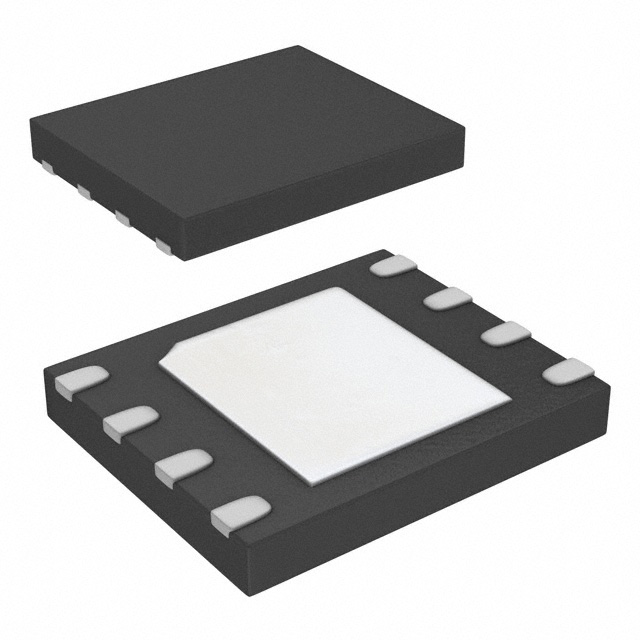


 工商网监
湘ICP备2023018690号
工商网监
湘ICP备2023018690号
