Obsolete Device
Please contact Microchip Sales for replacement information.
16 Mbit LPC Flash
SST49LF160C
EOL Data Sheet
SST49LF160C flash memory device is designed to interface with host controllers
(chipsets) that support a low pin-count (LPC) interface for system firmware applications. SST49LF160C device complies with the LPC Interface Specification. The
LPC interface operates with 5 signal pins versus 32 pins of a 8-bit parallel flash
memory. This frees up pins on the ASIC host controller resulting in lower ASIC
costs and a reduction in overall system costs due to simplified signal routing.
Features
• Organized as 2M x8
• Superior Reliability
– Endurance: 100,000 Cycles (typical)
– Greater than 100 years Data Retention
• Conforms to LPC Interface Specification
– Support Single-Byte LPC Memory Read/Write Cycles
• Single 3.0-3.6V Read and Write Operations
– Active Read Current: 12 mA (typical)
– Standby Current: 10 µA (typical)
• LPC Mode
– 5-signal LPC bus interface for both in-system and factory programming using programmer equipment
– 33 MHz clock frequency operation
– WP#/AAI and TBL# pins provide hardware Write protect
for entire chip and/or top Boot Block
– Block Locking Registers for individual block Read-Lock,
Write-Lock, and Lock-Down protection
– 5 GPI pins for system design flexibility
– 4 ID pins for multi-chip selection
– Status register for End-of-Write detection
– Program-/Erase-Suspend
Read or Write to other blocks during
Program-/Erase-Suspend
• Uniform 4 KByte sectors
– 35 Overlay Blocks: one 16-KByte Boot Block, two 8KByte Parameter Blocks, one 32-Kbyte Parameter
Block, thirty-one 64-KByte Main Blocks.
• Fast Sector-Erase/Program Operation
– Sector-Erase Time: 18 ms (typical)
– Block-Erase Time: 18 ms (typical)
– Program Time: 7 µs (typical)
• Auto Address Increment (AAI) for Rapid Factory
Programming (High Voltage Enabled)
– RY/BY# pin for End-of-Write detection
– Multi-Byte Program
– Chip Rewrite Time: 4 seconds (typical)
• Two-cycle Command Set
• Security ID Feature
– 256-bit Secure ID space
- 64-bit Unique Factory Pre-programmed Device Identifier
- 192-bit User-Programmable OTP
©2016
• Low Power Consumption
• Packages Available
– 32-lead PLCC
• All non-Pb (lead-free) devices are RoHS compliant
www.microchip.com
DS20005099B
02/16
�16 Mbit LPC Flash
SST49LF160C
EOL Data Sheet
Product Description
The SST49LF160C flash memory device is designed to interface with host controllers (chipsets) that
support a low-pin-count (LPC) interface for system firmware applications. The SST49LF160C device
complies with the LPC Interface Specification. The LPC interface operates with 5 signal pins versus 32
pins of a 8-bit parallel flash memory. This frees up pins on the ASIC host controller resulting in lower
ASIC costs and a reduction in overall system costs due to simplified signal routing.
The SST49LF160C uses a 5-signal LPC interface to support both in-system and rapid factory programming using programmer equipment. A high voltage pin (WP#/AAI) is used to enable Auto Address
Increment (AAI) mode. The SST49LF160C offers hardware block protection in addition to individual
block protection via software registers for critical system code and data. A 256-bit Security ID space
with a 64-bit factory pre-programmed unique number and a 192-bit user programmable OTP area
enhances the user’s ability to use new security techniques and implement a new data protection
scheme. The SST49LF160C also provides general purpose inputs (GPI) for system design flexibility.
The SST49LF160C flash memory device is manufactured with SST’s proprietary, high-performance
SuperFlash® technology. The split-gate cell design and thick-oxide tunneling injector attain greater
reliability and manufacturability compared with alternative technology approaches. The SST49LF160C
device significantly improves performance and reliability, while lowering power consumption. The
SST49LF160C device writes (Program or Erase) in-system with a single 3.0-3.6V power supply. It uses
less energy during Erase and Program than alternative flash memory technologies.
The total energy consumed is a function of the applied voltage, current and time of application. Since
for any given voltage range, the SuperFlash technology uses less current to program and has a shorter
erase time, the total energy consumed during any Erase or Program operation is less than alternative
flash memory technologies.
The SuperFlash technology provides fixed Erase and Program time, independent of the number of
Erase/Program cycles that have performed. Therefore the system software or hardware does not have
to be calibrated or correlated to the cumulative number of erase cycles as is necessary with alternative
flash memory technologies, whose Erase and Program time increase with accumulated Erase/Program cycles. To protect against inadvertent write, the SST49LF160C device has on-chip hardware and
software write protection schemes. It is offered with a typical endurance of 100,000 cycles. Data retention is rated at greater than 100 years.
The SST49LF160C product provides a maximum program time of 10 µs per byte with a single-byte
Program operation; effectively 5 µs per byte with a dual-byte Program operation and 2.5 µs per byte
with a quad-byte Program operation. End-of-Write can be detected by the RY/BY# pin output in AAI
mode and by reading the software status register during an in-system Program or Erase operation.
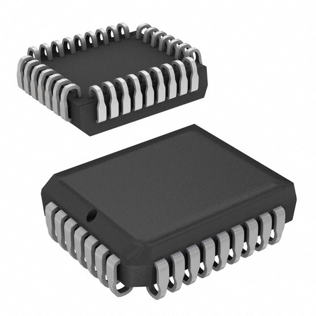
The SST49LF160C is offered in a 32-PLCC lead-free package to address the growing need for non-Pb
solutions in electronic components. Non-Pb package versions can be obtained by ordering products
with a package code suffix of “E” as the environmental attribute in the product part number. See Figure
3 for pin assignments and Table 1 for pin descriptions.
©2016
DS20005099B
2
02/16
�16 Mbit LPC Flash
SST49LF160C
EOL Data Sheet
Functional Blocks
TBL#
WP#
INIT#
X-Decoder
SuperFlash
Memory
LAD[3:0]
LCLK
LFRAME#
LPC
Interface
Address Buffers & Latches
Y-Decoder
ID[3:0]
GPI[4:0]
AAI
Control Logic
I/O Buffers and Data Latches
AAI
Interface
RY/BY#
LD#
RST#
1315 B1.0
Figure 1: Functional Block Diagram
©2016
DS20005099B
3
02/16
�16 Mbit LPC Flash
SST49LF160C
EOL Data Sheet
Device Memory Map
1FFFFFH
Block 34
11FFFFH
Block 17
Boot Block
1FC000H
1FBFFFH
110000H
10FFFFH
Block 16
Block 33
1FA000H
1F9FFFH
100000H
0FFFFFH
Block 15
Block 32
1F8000H
1F7FFFH
0F0000H
0EFFFFH
Block 14
Block 31
1F0000H
1EFFFFH
0E0000H
0DFFFFH
Block 13
Block 30
1E0000H
1DFFFFH
Block 12
Block 29
1D0000H
1CFFFFH
Block 11
Block 28
Block 27
WP# for
Block 0~33
Block 26
Block 25
Block 24
Block 23
Block 22
Block 21
Block 20
Block 19
Block 18
1C0000H
1BFFFFH
Block 10
1B0000H
1AFFFFH
Block 9
1A0000H
19FFFFH
Block 8
190000H
18FFFFH
WP# for
Block 0~33
180000H
17FFFFH
Block 7
Block 6
170000H
16FFFFH
Block 5
160000H
15FFFFH
Block 4
150000H
14FFFFH
Block 3
140000H
13FFFFH
Block 2
130000H
12FFFFH
Block 1
120000H
Block 0
(64 KByte)
0D0000H
0CFFFFH
0C0000H
0BFFFFH
0B0000H
0AFFFFH
0A0000H
09FFFFH
090000H
08FFFFH
080000H
07FFFFH
070000H
06FFFFH
060000H
05FFFFH
050000H
04FFFFH
040000H
03FFFFH
030000H
02FFFFH
020000H
01FFFFH
010000H
00FFFFH
4 KByte Sector 15
002000H
4 KByte Sector 2
001000H
4 KByte Sector 1
000000H
4 KByte Sector 0
1315 F16.0
TBL#
Figure 2: Device Memory Map for SST49LF160C
©2016
DS20005099B
4
02/16
�16 Mbit LPC Flash
SST49LF160C
EOL Data Sheet
NC
2
1
GPI4
RST#
3
LCLK
GPI3
4
NC
GPI2
Pin Assignments
32 31 30
29
NC
6
28
NC
WP#/AAI
7
27
NC
TBL#
8
26
NC
ID3
9
25
VDD
ID2
10
24
INIT#
ID1
11
23
ID0
12
22
LFRAME#
NC
LAD0
13
21
14 15 16 17 18 19 20
GPI1 (LD#)
5
GPI0 (RY/BY#)
32-lead PLCC
Top View
NC
NC
NC
NC
VSS
LAD3
LAD1
LAD2
1315 32-plcc P2.0
( ) Designates AAI Mode
Figure 3: Pin Assignments for 32-lead PLCC
©2016
DS20005099B
5
02/16
�16 Mbit LPC Flash
SST49LF160C
EOL Data Sheet
Pin Descriptions
Table 1: Pin Description
Interface
Symbol Pin Name
LCLK
Clock
LAD[3:0] Address
and Data
LFRAME Frame
#
RST#
Reset
INIT#
Initialize
Type1
I
I/O
AAI
X
X
I
X
I
I
X
X
X
ID[3:0]
Identification
Inputs
I
GPI[4:0]
General
Purpose
Inputs
I
TBL#
Top Block Lock
I
WP#/AAI Write Protect
I
WP#/AAI AAI Enable
I
X
RY/BY#
Ready/Busy#
O
X
LD#
Load-Enable#
I
X
VDD
VSS
NC
Power Supply
Ground
No Connection
PWR
PWR
X
X
N/A
LPC Functions
X
To accept a clock input from the control unit
X
To provide LPC bus information, such as addresses and command Inputs/Outputs data.
X
To indicate the start of a data transfer operation;
also used to abort an LPC cycle in progress.
X
To reset the operation of the device
X
This is the second reset pin for in-system use.
This pin is internally combined with the RST# pin.
If this pin or RST# pin is driven low, identical operation is exhibited.
X
These four pins are part of the mechanism that allows multiple
parts to be attached to the same bus. The strapping of these
pins is used to identify the component. The boot device must
have ID[3:0]=0000, all subsequent devices should use
sequential up-count strapping. These pins are internally
pulled-down with a resistor between 20-100 K.
X
These individual inputs can be used for additional board flexibility. The state of these pins can be read through LPC registers. These inputs should be at their desired state before the
start of the LPC clock cycle during which the read is
attempted, and should remain in place until the end of the
Read cycle. Unused GPI pins must not be floated.
GPI[2:4] are ignored when in AAI mode.
X
When low, prevents programming to the boot block sectors at
top of device memory. When TBL# is high it disables hardware
write protection for the top block sectors. This pin cannot be
left unconnected. TBL# setting is ignored when in AAI mode.
X
When low, prevents programming to all but the highest
addressable block (Boot Block). When WP# is high it disables
hardware write protection for these blocks. This pin cannot be
left unconnected.
When set to the Supervoltage VH = 9V, configures the device
to program multiple bytes in AAI mode. When brought to VIL/
VIH, returns device to LPC mode.
Open drain output that indicates the device is ready to accept data
in an AAI mode, or that the internal cycle is complete. Used in conjunction with LD# pin to switch between these two flag states.
Input pin which when low, indicates the host is loading data in
an AAI programming cycle. If LD# is high, the host signals the
AAI interface that it is terminating a command. LD# low/high
switches the RY/BY# output from a “buffer free” flag to a “programming complete” flag.
X
To provide power supply (3.0-3.6V)
X
Circuit ground (0V reference)
N/A Unconnected pins.
T1.2 25099
1. I=Input, O=Output
©2016
DS20005099B
6
02/16
�16 Mbit LPC Flash
SST49LF160C
EOL Data Sheet
Clock
The LCLK pin accepts a clock input from the host controller.
Input/Output Communications
The LAD[3:0] pins are used to serially communicate cycle information such as cycle type, cycle direction, ID selection, address, data, and sync fields.
Input Communication Frame
The LFRAME# pin is used to indicate start of a LPC bus cycle. The pin is also used to abort an LPC
bus cycle in progress.
Reset
A VIL on INIT# or RST# pin initiates a device reset. INIT# and RST# pins have the same function internally. It is required to drive INIT# or RST# pins low during a system reset to ensure proper CPU initialization. During a Read operation, driving INIT# or RST# pins low deselects the device and places the
output drivers, LAD[3:0], in a high impedance state. The reset signal must be held low for a minimum
of time TRSTP. A reset latency occurs if a reset procedure is performed during a Program or Erase operation. See Table 27, Reset Timing Parameters, for more information. A device reset during an active
Program or Erase operation will abort the operation and memory contents may become invalid due to
data being altered or corrupted from an incomplete Erase or Program operation.
Identification Inputs
These pins are part of a mechanism that allows multiple devices to be attached to the same bus. The
strapping of these pins is used to identify the component. The boot device must have ID[3:0] = 0; all
subsequent devices should use sequential count-up strapping. These pins are internally pulled-down
with a resistor between 20-100 K.
General Purpose Inputs
The General Purpose Inputs (GPI[4:0]) can be used as digital inputs for the CPU to read. The GPI register holds the values on these pins. The data on the GPI pins must be stable before the start of a GPI
register Read and remain stable until the Read cycle is complete. The pins must be driven low, VIL, or
high, VIH but not left unconnected (float).
In the Auto Address Increment (AAI) mode, GPI0 is used as Ready/Busy (RY/BY#), and GPI1 is used
as Load Enable (LD#).
©2016
DS20005099B
7
02/16
�16 Mbit LPC Flash
SST49LF160C
EOL Data Sheet
Write Protect / Top Block Lock
The Top Boot Lock (TBL#) and Write Protect (WP#/AAI) pins are provided for hardware write protection of device memory in the SST49LF160C. The TBL# pin is used to write protect 16 KByte at the
highest memory address range for the SST49LF160C. WP#/AAI pin write protects the remaining sectors in the flash memory. An active low signal at the TBL# pin prevents Program and Erase operations
of the top Boot Block. When TBL# pin is held high, write protection of the top Boot Block is then determined by the Boot Block Locking registers. The WP#/AAI pin serves the same function for the remaining sectors of the device memory. The TBL# and WP#/AAI pins write protection functions operate
independently of one another. Both TBL# and WP#/AAI pins must be set to their required protection
states prior to starting a Program or Erase operation. A logic level change occurring at the TBL# or
WP#/AAI pin during a Program or Erase operation could cause unpredictable results. TBL# and WP#/
AAI pins cannot be left unconnected.
TBL# is internally OR’ed with the top Boot Block Locking register. When TBL# is low, the top Boot
Block is hardware write protected regardless of the state of the Write-Lock bit for the Boot Block Locking register. Clearing the Write-Protect bit in the register when TBL# is low will have no functional
effect, even though the register may indicate that the block is no longer locked.
WP#/AAI is internally OR’ed with the Block Locking register. When WP#/AAI is low, the blocks are
hardware write protected regardless of the state of the Write-Lock bit for the corresponding Block
Locking registers. Clearing the Write-Protect bit in any register when WP#/AAI is low will have no functional effect, even though the register may indicate that the block is no longer locked.
AAI Enable
The AAI Enable pin (WP#/AAI) is used to enable the Auto Address Increment (AAI) mode. When the
WP#/AAI pin is set to the Supervoltage VH (9±0.5V), the device is in AAI mode with Multi-Byte programming. When the WP#/AAI pin is brought to VIL/VIH levels, the device returns to LPC mode.
Ready/Busy
The Ready/Busy pin (RY/BY#), is an open drain output which indicates either the device is ready to
accept data in AAI mode, or that the internal programming cycle is complete. The pin is used in conjunction with the LD# pin to switch between these two flag states (see Table 18).
Load Enable
The Load Enable pin (LD#), is an input pin which when low, indicates the host is loading data in an AAI
programming cycle. Data is loaded in the SST49LF160C at the rising edge of the clock. If LD# is high, it
signals the AAI interface that the host is terminating the command. LD# low/high switches the RY/BY#
output from buffer free flag to programming complete flag (see Table 18).
No Connection (NC)
These pins are not connected internally.
©2016
DS20005099B
8
02/16
�16 Mbit LPC Flash
SST49LF160C
EOL Data Sheet
Design Considerations
SST recommends a high frequency 0.1 µF ceramic capacitor to be placed as close as possible
between VDD and VSS less than 1 cm away from the VDD pin of the device. Additionally, a low frequency 4.7 µF electrolytic capacitor from VDD to VSS should be placed within 1 cm of the VDD pin. If you
use a socket for programming purposes add an additional 1-10 µF next to each socket.
The RST# pin must remain stable at VIH for the entire duration of an Erase operation. WP#/AAI must
remain stable at VIH for the entire duration of the Erase and Program operations for non-Boot Block
sectors. To write data to the top Boot Block sectors, the TBL# pin must also remain stable at VIH for the
entire duration of the Erase and Program operations.
Mode Selection
The SST49LF160C flash memory device operates in two distinct interface modes: the LPC mode and
the Auto Address Increment (AAI) mode. The WP#/AAI pin is used to set the interface mode selection.
The device is in AAI mode when the WP#/AAI pin is set to the Supervoltage VH (9±0.5V), and in the
LPC mode when the WP#/AAI is set to VIL/VIH. The mode selection must be configured prior to device
operation.
©2016
DS20005099B
9
02/16
�16 Mbit LPC Flash
SST49LF160C
EOL Data Sheet
LPC Mode
Device Operation
The SST49LF160C supports Single-Byte LPC Memory Read and Write cycle types as defined in Low
Pin Count Interface Specification. Table 2 shows the size of transfer supported by the SST49LF160C.
Table 2: Transfer Size Supported
Cycle Type
Size of Transfer
LPC Memory Read
1 Byte
LPC Memory Write
1 Byte
T2.0 25099
The LPC mode uses a 5-signal communication interface: one control line, LFRAME#, which is driven
by the host to start or abort a bus cycle, a 4-bit data bus, LAD[3:0], used to communicate cycle type,
cycle direction, ID selection, address, data and sync fields. The device enters standby mode when
LFRAME# is taken high and no internal operation is in progress.
The host drives LFRAME# signal from low-to-high to capture the start field of a LPC cycle. On the
cycle in which LFRAME# goes inactive, the last latched value is taken as the START value. The START
value determines whether the SST49LF160C will respond to a LPC Memory Read/Write cycle type as
defined in Table 3.
Table 3: LPC Memory Cycles START Field Definition
START Value
0000
Definition
Start of an LPC memory cycle. The direction (Read or Write) is determined by the second field
of the LPC cycle.
T3.1 25099
See following sections on details of LPC Memory cycle types (Tables 4 and 5). Two-cycle Program and
Erase command sequences are used to initiate LPC Memory Program and Erase operations. See Table 8 for
a listing of Program and Erase commands.
©2016
DS20005099B
10
02/16
�16 Mbit LPC Flash
SST49LF160C
EOL Data Sheet
LPC Memory Cycles
LPC Memory Read Cycle
Table 4: LPC Memory Read Cycle Field Definitions
Clock
Cycle
Field
Name
Field
Contents
LAD[3:0]1
LAD[3:0]
Direction
1
START
0000
IN
LFRAME# must be active (low) for the device to respond.
Only the last field latched before LFRAME# transitions high
will be recognized. The START field contents (0000b) indicate
an LPC Memory cycle.
2
CYCTYPE +
DIR
010X
IN
Indicates the type of LPC Memory cycle. Bits 3:2 must be “01b” for
memory cycle. Bit 1 indicates the type of transfer “0” for Read. Bit 0
is reserved.
3-10
ADDR
YYYY
IN
Address Phase for Memory Cycle. LPC protocol supports a
32-bit address phase. YYYY is one nibble of the entire
address. Addresses are transferred most-significant nibble
first. The SST49LF160C encodes ID and register space
access in the address fields.
11
TAR0
1111
IN
then Float
In this clock cycle, the host drives the bus to all 1s and then floats
the bus. This is the first part of the bus “turnaround cycle.”
12
TAR1
1111 (float)
Float
then OUT
The SST49LF160C takes control of the bus during this cycle.
13
RSYNC
0000
OUT
The SST49LF160C outputs the value 0000b indicating that it
has received data.
Comments
14
DATA
ZZZZ
OUT
ZZZZ is the least-significant nibble of the data byte.
15
DATA
ZZZZ
OUT
ZZZZ is the most-significant nibble of the data byte.
16
TAR0
1111
OUT,
then Float
17
TAR1
1111 (float)
Float,
then IN
In this clock cycle, the SST49LF160C drives the bus to all 1s
and then floats the bus. This is the first part of the bus “turnaround cycle.”
The host takes control of the bus during this cycle.
T4.0 25099
1. Field contents are valid on the rising edge of the present clock cycle.
1
2
7
8
9
A[31:28] A[27:24] A[23:20] A[19:16] A[15:12]
A[11:8]
A[7:4]
3
4
5
6
10
12
11
13
14
15
16
17
LCLK
LFRAME#
LAD[3:0]
Start
CYCTYPE
+
DIR
0000b
010Xb
1 Clock 1 Clock
Address
Load Address in 8 Clocks
A[3:0]
TAR0
TAR1
1111b
Tri-State
2 Clocks
Sync
0000b
Data
D[3:0]
D[7:4]
TAR
1 Clock Data Out 2 Clocks
1315 F05.1
Figure 4: LPC Memory Read Cycle Waveform
©2016
DS20005099B
11
02/16
�16 Mbit LPC Flash
SST49LF160C
EOL Data Sheet
LPC Memory Write Cycle
Table 5: LPC Memory Write Cycle Field Definitions
Clock
Cycle
Field
Name
Field
Contents
LAD[3:0]1
LAD[3:0]
Direction
1
START
0000
IN
LFRAME# must be active (low) for the part to
respond.
Only the last start field latched before LFRAME# transitional high will be recognized. The START field contents (0000b) indicate an LPC Memory cycle.
2
CYCTYPE+
DIR
011X
IN
Indicates the type of LPC Memory cycle. Bits 3:2
must be “01b” for memory cycle. Bit 1 indicates the
type of transfer “1” for Write. Bit 0 is reserved.
3-10
ADDR
YYYY
IN
Address Phase for Memory Cycle. LPC protocol supports a 32-bit address phase. YYYY is one nibble of
the entire address. Addresses are transferred mostsignificant nibble first. The SST49LF160C encodes ID
and register space access in the address fields.
Comments
11
DATA
ZZZZ
IN
ZZZZ is the least-significant nibble of the data byte.
12
DATA
ZZZZ
IN
ZZZZ is the most-significant nibble of the data byte.
13
TAR0
1111
IN then Float
In this clock cycle, the host has driven the bus to all 1s
and then floats the bus. This is the first part of the bus
“turnaround cycle.”
14
TAR1
1111 (float)
Float then
OUT
The SST49LF160C takes control of the bus during this
cycle.
15
RSYNC
0000
OUT
The SST49LF160C outputs the value 0000b indicating
that it has received data or a flash command.
16
TAR0
1111
OUT, then
float
In this clock cycle, the SST49LF160C drives the bus
to all 1s and then floats the bus. This is the first part of
the bus “turnaround cycle.”
17
TAR1
1111 (float)
Float, then IN The host resumes control of the bus during this cycle.
T5.0 25099
1. Field contents are valid on the rising edge of the present clock cycle.
1
2
3
4
5
6
7
8
9
A[11:8]
A[7:4]
10
11
12
13
14
15
16
17
LCLK
LFRAME#
LAD[3:0]
Start
CYCTYPE
+
DIR
0000b
011Xb
1 Clock 1 Clock
Address
A[31:28] A[27:24] A[23:20] A[19:16] A[15:12]
Load Address in 8 Clocks
A[3:0]
Data
Data
TAR0
D[3:0]
D[7:4]
1111b Tri-State
Load Data in 2 Clocks
TAR1
2 Clocks
Sync
0000b
TAR
1 Clock
1315 F06.1
Figure 5: LPC Memory Write Cycle Waveform
©2016
DS20005099B
12
02/16
�16 Mbit LPC Flash
SST49LF160C
EOL Data Sheet
Abort Mechanism
If LFRAME# is driven low for one or more clock cycles after the start of a bus cycle, the cycle will be
terminated. The host may drive the LAD[3:0] with ‘1111b’ (ABORT nibble) to return the interface to
ready mode. The ABORT only affects the current bus cycle. For a multi-cycle command sequence,
such as the Erase or Program commands, ABORT doesn’t interrupt the entire command sequence,
only the current bus cycle of the command sequence. The host can re-send the bus cycle for the
aborted command and continue the command sequence after the device is ready again.
Response to Invalid Fields for LPC Memory Cycle
During an on-going LPC bus cycle, the SST49LF160C will not explicitly indicate that it has received
invalid field sequences. The response to specific invalid fields or sequences is described as follows:
ID mismatch:
ID information is included in the address bits of every LPC Memory cycle. Address bits [A25:A23, A21]
are used to select the device with proper IDs. The SST49LF160C will compare the ID bits in the
address field with ID[3:0]. If the ID bits in the address do not correspond to the hardware ID pins the
device will ignore the cycle. See Device Commands section for details.
Address out of range:
The address sequence is 8 fields long (32 bits). The address bits [A25:A23, A21] for the SST49LF160C
are used to select the device with proper IDs. Unused most significant address bits must be set to “1”
during LPC protocol transfer. Address A22 has the special function of directing Read and Write operations to the flash core (A22=1) or to the register space (A22=0).
For the Boot Device (ID[3:0]=0000b), the SST49LF160C decodes the physical addresses of the Top
128 KByte Blocks (including Boot Block) at both system memory ranges indicated in Table 6.
Table 6: Boot Device Physical Addresses Decoding
Memory Range
Also mapped at Memory Range
FFFF FFFFH - FFFE 0000H
000F FFFFH - 000E 0000H
Once valid START, CYCTYPE + DIR, and address range (including ID bits) are received, the
SST49LF160C will always complete the bus cycle. However, if the device is busy performing a flash
Erase or Program operation, no new internal memory Write will be executed. As long as the states of
LAD[3:0] and LFRAME# are known, the response of the SST49LF160C to signals received during the
LPC cycle is predictable.
©2016
DS20005099B
13
02/16
�16 Mbit LPC Flash
SST49LF160C
EOL Data Sheet
Multiple Device Selection
Multiple LPC flash devices may be strapped to increase memory densities in a system. The four ID
pins, ID[3:0], allow up to 16 devices to be attached to the same bus by using different ID strapping in a
system. BIOS support, bus loading, or the attaching bridge may limit this number. The boot device
must have an ID of 0000b (determined by ID[3:0]); subsequent devices use incremental numbering.
Equal density must be used with multiple devices.
Multiple Device Selection for LPC Memory Cycle
For LPC Memory Read/Write cycles, ID information is included in the address bits of every cycle. The
ID bits in the address field are inverse of the hardware strapping. The address bits [A25:A23, A21] are
used to select the device with proper IDs. See Table 7 for device selection configurations. The
SST49LF160C will compare these bits with ID[3:0]’s strapping values. If there is a mismatch, the
device will ignore the remainder of the cycle.
Table 7: LPC Memory Multiple Device Selection Configuration
Hardware Strapping
ID Address Bits
ID[3:0]
A25:A23, A21
0 (Boot device)
0000
1111
1
0001
1110
2
0010
1101
3
0011
1100
4
0100
1011
5
0101
1010
6
0110
1001
7
0111
1000
8
1000
0111
9
1001
0110
10
1010
0101
11
1011
0100
12
1100
0011
13
1101
0010
14
1110
0001
15
1111
0000
Device #
T7.0 25099
©2016
DS20005099B
14
02/16
�16 Mbit LPC Flash
SST49LF160C
EOL Data Sheet
Device Commands
Device operation is controlled by commands written to the Command User Interface (CUI). Execution
of a specific command is handled by internal functions after a CUI receives and processes the command. After power-up or a Reset operation the device enters Read mode. Commands consist of one
or two sequential Bus-Write operations. The commands are summarized in Table 8, “Software Command Sequence”.
Table 8: Software Command Sequence
Bus Cycles
Required
First Bus Cycle
Oper
Addr1
Data
1
Write
X
FFH
2
Write
X
Read-Status-Register3
2
Write
Clear-Status-Register
1
Sector-Erase7
2
Block-Erase7
Program7,9
Second Bus Cycle
Oper
Addr1
Data
90H
Read
IA4
ID5
X
70H
Read
X
SRD6
Write
X
50H
Write
X
30H
Write
SAx8
D0H
2
Write
X
20H
Write
BAx
D0H
2
Write
X
40H
or
10H
Write
WA10
WD11
Program-/Erase-Suspend
1
Write
X
B0H
Program-/Erase-Resume
1
Write
X
D0H
User-Security-ID-Program12
2
Write
X
A5H
Write
WA10
Data
User-Security-ID-Program-Lockout
2
Write
X
85H
Write
X
Command
Read-Array/Reset
Read-Software-ID2/
Read-Security-ID3
00H
T8.0 25099
1. This value must be a valid address within the device Memory Address Space. X can be VIH or VIL, but no other value.
2. SST Manufacturer’s ID = BFH, is read with A20-A0 = 0.
SST49LF160C Device ID = 4CH, is read with A20-A1 = 0, A0 = 1.
Following the Read-Software-ID/Read-Security-ID command,
Read operations access Manufacturer’s ID and Device ID or Security ID.
3. Following the Read-Software-ID/Read-Security-ID command, Read operations access manufacturer’s ID and Device ID
or Security ID. Read-Software-ID/Read-Security-ID and Read-Status-Register will return register data until another
valid command is written.
4. IA = Device Identification Address/Security ID Address.
5. ID = Data read from identifier codes/Data read from Security ID
6. SRD = Data read from Status register
7. The sector or block must not be write-locked when attempting Erase or Program operations.
Attempts to issue an Erase or Program command to a write-locked sector/block will fail.
8. SAX for Sector-Erase Address
BAX for Block-Erase Address
9. The Program command operates on one byte at a time.
10. WA = Address of memory location to be written
11. WD = Data to be written at location WA
12. Valid addresses for the User Security ID space are from FFFC 0188H to FFFC 019FH.
©2016
DS20005099B
15
02/16
�16 Mbit LPC Flash
SST49LF160C
EOL Data Sheet
Read-Array Command
Upon initial device power-up and after exit from reset, the device defaults to the read array mode. This
operation can also be initiated by writing the Read-Array command. (See Table 8.) The device remains
available for array reads until another command is written. Once an internal Program/Erase operation
starts, the device will not recognize the Read-Array command until the operation is completed, unless
the operation is suspended via a Program/Erase Suspend command.
Read-Software-ID Command
The Read-Software-ID operation is initiated by writing the Read-Software-ID command. Following the
command, the device will output the manufacturer’s ID and device ID from the addresses shown in
Table 9. Any other valid command will terminate the Read-Software-ID operation.
The Read-Software-ID command is the same as the Read-Security-ID command. See “Security ID
Commands” on page 18.
Table 9: Product Identification
Manufacturer’s ID
Address1
Data
FFFC 0000H
BFH
FFFC 0001H
4CH
Device ID
SST49LF160C
T9.1 25099
1. Address shown in this column is for boot device only. Address locations should appear elsewhere in the 4 GByte system
memory map depending on ID strapping values on ID[3:0] pins when multiple LPC memory devices are used in a system.
Read-Status-Register Command
The Status register may be read to determine when a Sector-/Block-Erase or Program completes, and
whether the operation completed successfully. The Status register may be read at any time by writing
the Read-Status-Register command. After writing this command, all subsequent Read operations will
return data from the Status register until another valid command is written.
The default value of the Status register after device power-up or reset is 80H.
©2016
DS20005099B
16
02/16
�16 Mbit LPC Flash
SST49LF160C
EOL Data Sheet
Clear-Status-Register Command
The user can reset the Status register’s Block Protect Status (BPS) bit to 0 by issuing a Clear-StatusRegister command. Device power-up and hardware reset will also reset BPS to 0.
Table 10: Software Status Register
Bit
Name
Function
0
RES
Reserved for future use
1
BPS
Block Protect Status
The Block Write-Lock bit should be interrogated only after Erase or Program command is issued.
It informs the system whether or not the selected block is locked.
BPS does not provide a continuous indication of Write-Lock bit value.
0: Block Unlocked
1: Operation Aborted, Block Write-Lock bit set.
2:5
RES
Reserved for future use
6
ESS
Erase Suspend Status
0: Erase in progress/completed
1: Erase suspended
7
WSMS Write State Machine Status
Check WSMS to determine erase or program completion.
0: Busy
1: Ready
T10.0 25099
Sector-/Block-Erase Command
The Erase Command operates on one sector or block at a time. This command requires an (arbitrary)
address within the sector or block to be erased. Note that a Sector/Block Erase operation changes all
Sector/Block byte data to FFh. If a Read operation is performed after issuing the erase command, the
device will automatically output Status Register data. The system can poll the Status Register in order
to verify the completion of the Sector/Block Erase operation (please refer to Table 10, Status Register
Definition). If a Sector/Block Erase is attempted on a locked block, the operation will fail and the data in
the Sector/Block will not be changed. In this case, the Status Register will report the error (BPS=1).
Program Command
The Program command operates on one byte at a time (Refer to Table 5). This command specifies the
address and data to be programmed. During the Program operation the device automatically outputs
the Status Register data when read. The system can poll the Status Register in order to verify the completion of the Program operation (refer to Table 10, “Software Status Register”). If a Program operation
is attempted on a locked block, the operation will fail and the data in the addressed byte will not be
changed. In this case, the Status Register will report the error (BPS=1).
Program-/Erase-Suspend or Program-/Erase-Resume Operations
The Program-Suspend and Erase-Suspend operations share the same software command sequence
(B0H). The Program-Resume and Erase-Resume operations share the same software command
sequence (D0H). See Table 8, “Software Command Sequence” on page 15.
©2016
DS20005099B
17
02/16
�16 Mbit LPC Flash
SST49LF160C
EOL Data Sheet
Erase-Suspend/Erase-Resume Commands
The Erase Suspend command allows Sector-Erase or Block-Erase interruption in order to read or program data in another block of memory. Once the Erase-Suspend command is executed, the device will
suspend any on-going Erase operation within time TES (10 µs). The device outputs status register data
when read after the Erase-Suspend command is written. The system is able to determine when the
Erase operation has been completed (WSMS=1) by polling the status register. After an Erase-Suspend, the device will set the status register ESS bit (ESS=1) if the Erase has been successfully suspended (refer to Table 10, “Software Status Register”). The Erase-Resume command resumes the
Erase operation that had been previously suspended.
After a successful Erase-Suspend, a Read-Array command may be written to read data from a Sector/
Block other than the suspended Sector/Block. A Program command sequence may also be issued
during Erase Suspend to program data in memory locations other than the Sector/Block currently in
the Erase-Suspend mode. If a Read-Array command is written to an address within the suspended
Sector/Block this may result in reading invalid data. If a Program command is written to an address
within the suspended Sector/Block the command is acknowledged but rejected. Other valid commands
while erase is suspended include Read-Status-Register, Read-Device-ID, and Erase-Resume.
The Erase-Resume command resumes the Erase process in the suspended sector or block. After the
Erase-Resume command is written, the device will continue the Erase process. Erase cannot resume
until any Program operation initiated during Erase-Suspend has completed. Suspended operations
cannot be nested: the system needs to complete or resume any previously suspended operation
before a new operation can be suspended. See Figure 6 for flowchart.
Program-Suspend/Program-Resume Command
The Program-Suspend and Program-Resume commands have no influence on the device. Since the
device requires a maximum of TBP (10 µs) in order to program a byte (see Table 28), when a ProgramSuspend command is written, the suspended Byte Program operation will always be successfully completed within the suspend latency time (TES = TBP = 10 µs).
Security ID Commands
The SST49LF160C device offers a 256-bit Security ID space. The Security ID space is divided into two
parts. One 64-bit segment is programmed at SST with a unique 64-bit number: this number cannot be
changed by the user. The other segment is 192-bit wide and is left blank: this space is available for
customers and can be programmed as desired.
The User-Security-ID-Program command is shown in Table 8, “Software Command Sequence”. Use
the memory addresses specified in Table 11 for Security ID programming. Once the customer segment
is programmed, it can be locked to prevent any alteration. The User-Security-ID-Program-Lockout
command is shown in Table 8, “Software Command Sequence”.
In order to read the Security ID information, the user can issue a Read Security ID Command (90H) to
the device. At this point the device enters the Read-Software-ID/Read-Security-ID mode. The Security
ID information can be read at the memory addresses in Table 11.
A Read-Array/Reset command (FFH) must then be issued to the device in order to exit the Read-Software-ID/Read-Security-ID mode and return to Read-Array mode.
An alternate method to read the Security ID information is to read the Security ID registers located into
the register space as described in the “Security ID Registers” section.
©2016
DS20005099B
18
02/16
�16 Mbit LPC Flash
SST49LF160C
EOL Data Sheet
Erase Sector/Block
Write B0H to any valid
device memory address
Erase-Suspend
Command
Write 70H to any valid
device memory address
Read-Status-Register
Command
Read Status Register
No
WSMS = 1
Yes
ESS = 1
Erase Completed
No
Yes
Write the Read-Array
command to read from
another Sector/Block
or
Write the Program
command to program
another Sector/Block
No
Finished?
Yes
Write D0H to any valid
device memory address
Erase-Resume
Command
Erase Resumed
1315 FC_Erase-Sus.1
Figure 6: Erase-Suspend Flow Chart
Table 11: Security ID Addresses
Address Range
Security ID Segment
Size
FFFC 0180 to FFFC 0187
Factory-Programmed
8 bytes – 64 bit
FFFC 0188 to FFFC 019F
User-Programmed
24 bytes – 192 bit
T11.0 25099
©2016
DS20005099B
19
02/16
�16 Mbit LPC Flash
SST49LF160C
EOL Data Sheet
Registers
There are four types of registers available on the SST49LF160C, General Purpose Inputs registers,
Block Locking registers, Security ID register, and the JEDEC ID registers. These registers appear at
their respective address location in the 4 GByte system memory map. Unused register locations will
read as 00H. Any attempt to read or write any register during an internal Write operation will be
ignored.
Read or write access to the register during an internal Program/Erase operation will be completed as
follows:
•
•
General Purpose Inputs register, and Block Locking registers can be accessed normally
Security ID register and the JEDEC ID registers can not be accessed (reading these registers will return unused register data 00H).
General Purpose Inputs Register
The General Purpose Inputs register (GPI_REG) passes the state of GPI[4:0] pins on the
SST49LF160C. It is recommended that the GPI[4:0] pins be in the desired state before LFRAME# is
brought low for the beginning of the bus cycle, and remain in that state until the end of the cycle. There
is no default value since this is a pass-through register. The GPI_REG register for the boot device
appears at FFBC0100H in the 4 GByte system memory map, and will appear elsewhere if the device is
not the boot device (see Table 12). This register is not available to be read when the device is in an
Erase/Program operation.
Table 12: General Purpose Register
Register
Register Address1
Default
Value
Access
GPI_REG
FFBC 0100H
N/A
R
T12.0 25099
1. Address shown in this column is for boot device only. Address locations should appear elsewhere in the 4 GByte system memory map depending on ID strapping values on ID[3:0] pins when multiple LPC memory devices are used in a
system.
©2016
DS20005099B
20
02/16
�16 Mbit LPC Flash
SST49LF160C
EOL Data Sheet
Block Locking Registers
SST49LF160C provides software controlled lock protection through a set of Block Locking registers.
The Block Locking Registers are read/write registers and they are accessible through standard
addressable memory locations specified in Table 13. Unused register locations will return 00H if read.
Table 13: Block Locking Registers
Register
T_BLOCK_LK
T_MINUS01_LK
T_MINUS02_LK
T_MINUS03_LK
T_MINUS04_LK
T_MINUS05_LK
T_MINUS06_LK
T_MINUS07_LK
T_MINUS08_LK
T_MINUS09_LK
T_MINUS10_LK
T_MINUS11_LK
T_MINUS12_LK
T_MINUS13_LK
T_MINUS14_LK
T_MINUS15_LK
T_MINUS16_LK
T_MINUS17_LK
T_MINUS18_LK
T_MINUS19_LK
T_MINUS20_LK
T_MINUS21_LK
T_MINUS22_LK
T_MINUS23_LK
T_MINUS24_LK
T_MINUS25_LK
T_MINUS26_LK
T_MINUS27_LK
T_MINUS28_LK
T_MINUS29_LK
T_MINUS30_LK
T_MINUS31_LK
T_MINUS32_LK
T_MINUS33_LK
T_MINUS34_LK
Block Size
16K
8K
8K
32K
64K
64K
64K
64K
64K
64K
64K
64K
64K
64K
64K
64K
64K
64K
64K
64K
64K
64K
64K
64K
64K
64K
64K
64K
64K
64K
64K
64K
64K
64K
64K
SST49LF160C Protected Memory
Address1 Range
1FFFFFH-1FC000H
1FBFFFH-1FA000H
1F9FFFH-1F8000H
1F7FFFH-1F0000H
1EFFFFH-1E0000H
1DFFFFH-1D0000H
1CFFFFH-1C0000H
1BFFFFH-1B0000H
1AFFFFH-1A0000H
19FFFFH-190000H
18FFFFH-180000H
17FFFFH-170000H
16FFFFH-160000H
15FFFFH-150000H
14FFFFH-140000H
13FFFFH-130000H
12FFFFH-120000H
11FFFFH-110000H
10FFFFH-100000H
0FFFFFH-0F0000H
0EFFFFH-0E0000H
0DFFFFH-0D0000H
0CFFFFH-0C0000H
0BFFFFH-0B0000H
0AFFFFH-0A0000H
09FFFFH-090000H
08FFFFH-080000H
07FFFFH-070000H
06FFFFH-060000H
05FFFFH-050000H
04FFFFH-040000H
03FFFFH-030000H
02FFFFH-020000H
01FFFFH-010000H
00FFFFH-000000H
Memory Map Register
Address1
FFBFC002H
FFBFA002H
FFBF8002H
FFBF0002H
FFBE0002H
FFBD0002H
FFBC0002H
FFBB0002H
FFBA0002H
FFB90002H
FFB80002H
FFB70002H
FFB60002H
FFB50002H
FFB40002H
FFB30002H
FFB20002H
FFB10002H
FFB00002H
FFAF0002H
FFAE0002H
FFAD0002H
FFAC0002H
FFAB0002H
FFAA0002H
FFA90002H
FFA80002H
FFA70002H
FFA60002H
FFA50002H
FFA40002H
FFA30002H
FFA20002H
FFA10002H
FFA00002H
T13.0 25099
1. Address shown in this column is for boot device only. Address locations should appear elsewhere in the 4 GByte system memory map depending on ID strapping values on ID[3:0] pins when multiple LPC memory devices are used in a system.
©2016
DS20005099B
21
02/16
�16 Mbit LPC Flash
SST49LF160C
EOL Data Sheet
Table 14: Block Locking Register Bits
Reserved
Bit[7:3]
Read-Lock
Bit[2]
Lock-Down
Bit[1]
Write-Lock
Bit[0]
Lock Status
00000
0
0
0
Full Access
00000
0
0
1
Write Locked (Default State at Power-Up)
00000
0
1
0
Locked Open (Full Access Locked Down)
00000
0
1
1
Write Locked Down
00000
1
0
0
Block Read Locked (Registers alterable)
00000
1
0
1
Block Read & Write Lock (Registers alterable)
00000
1
1
0
Block Read Locked Down (Registers not alterable)
00000
1
1
1
Block Read & Write lock Down (Registers not
alterable)
T14.0 25099
Write-Lock Bit
The Write-Lock bit, bit 0, controls the lock state described in Table 14. The default Write status of all
blocks after power up is write locked. When bit 0 of the Block Locking register is set, Program and
Erase operations for the corresponding block are prevented. Clearing the Write-Lock bit will unprotect
the block. The Write-Lock bit must be cleared prior to starting a Program or Erase operation since it is
sampled at the beginning of the operation. The Write-Lock bit functions in conjunction with the hardware Write Lock pin TBL# for the top Boot Block. When TBL# is low, it overrides the software locking
scheme. The top Boot Block Locking register does not indicate the state of the TBL# pin. The WriteLock bit functions in conjunction with the hardware WP#/AAI pin for the remaining blocks (Blocks 0 to
33 for SST49LF160C). When WP#/AAI is low, it overrides the software locking scheme. The Block
Locking register does not indicate the state of the WP#/AAI pin.
Lock-Down Bit
The Lock-Down bit, bit 1, controls the Block Locking register as described in Table 14. When in LPC
interface mode, the default Lock Down status of all blocks upon power-up is not locked down. Once the
Lock-Down bit is set, any future attempted changes to that Block Locking register will be ignored. The
Lock-Down bit is only cleared upon a device reset with RST# or INIT# or power down. Current Lock
Down status of a particular block can be determined by reading the corresponding Lock-Down bit.
Once a block’s Lock-Down bit is set, the Read-Lock and Write-Lock bits for that block can no longer be
modified: the block is locked down in its current state of read/write accessibility.
Read-Lock Bit
The default read status of all blocks upon power-up is read-unlocked. When a block’s read lock bit is
set, data cannot be read from that block. An attempted read from a read-locked block will result in the
data 00h. The read lock status can be unlocked by clearing the read lock bit: this can only be done provided that the block is not locked down. The current read lock status of a particular block can be determined by reading the corresponding read-lock bit.
©2016
DS20005099B
22
02/16
�16 Mbit LPC Flash
SST49LF160C
EOL Data Sheet
Security ID Registers
The SST49LF160C device offers a 256-bit Security ID register space. The Security ID space is divided
into two segments - one (64-bits) factory programmed segment and one (192 bits) user programmed
segment. The first segment is programmed and locked at SST with a unique 64-bit number. The user
segment (192 bits) is left blank (FFH) for the customer to be programmed as desired. Refer to Table 8,
“Software Command Sequence” for more details.
The Security ID Information and its Write Lock/Unlock status can be Read in the Register Access
Space for Execute-In-Place type of applications. (See Table 15.)
The Write Lock-out status of the Security ID space can be read from the SEC_ID_WRITE_LOCK register (see Table 15). The SEC_ID_WRITE_LOCK register is a read-only register that is accessible at
the address location specified in Table 15.
Table 15: Security ID Registers
Register
Register
Address1
SEC_ID__WRITE_LOCK
FFBC0102H
SEC_ID_BYTE_0
SEC_ID_BYTE_1
Value
0000 0000b
0000 0001b
Access
Description
R
Write Unlocked
Write Locked
FFBC0180H
R
Factory Programmed
FFBC0181H
R
Factory Programmed
SEC_ID_BYTE_2
FFBC0182H
R
Factory Programmed
SEC_ID_BYTE_3
FFBC0183H
R
Factory Programmed
…
…
…
…
SEC_ID_BYTE_7
FFBC0187H
R
Factory Programmed
SEC_ID_BYTE_8
FFBC0188H
R
User Programmed
SEC_ID_BYTE_9
FFBC0189H
R
User Programmed
…
…
…
…
SEC_ID_BYTE_30
FFBC019EH
R
User Programmed
SEC_ID_BYTE_31
FFBC019FH
R
User Programmed
T15.0 25099
1. Address shown in this column is for boot device only. Address locations should appear elsewhere in the 4 GByte system memory map depending on ID strapping values on ID[3:0] pins when multiple LPC memory devices are used in a
system.
©2016
DS20005099B
23
02/16
�16 Mbit LPC Flash
SST49LF160C
EOL Data Sheet
JEDEC ID Registers
The JEDEC ID registers for the boot device appear at FFBC0000H and FFBC0001H in the 4 GByte
system memory map, and will appear elsewhere if the device is not the boot device, see Table 17. This
register is not available to be read when the device is in Erase/Program operation. Unused register
location will read as 00H. See Table 16 for the JEDEC device ID code.
Table 16: JEDEC ID Registers
Register Address1
Register
Default
Value
Access
MANUF_REG
FFBC 0000H
BFH
R
DEV_REG
FFBC 0001H
4CH
R
T16.0 25099
1. Address shown in this column is for boot device only. Address locations should appear elsewhere in the 4 GByte system memory map depending on ID strapping values on ID[3:0] pins when multiple LPC memory devices are used in a
system.
Table 17: LPC Memory Map Register Addresses
SST49LF160C
Hardware
Strapping
Device #
JEDEC ID
ID[3:0]
GPI_REG
MANUF_REG
DEV_REG
0 (Boot device)
0000
FFBC 0100H
FFBC 0000H
FFBC 0001H
1
0001
FF9C 0100H
FF9C 0000H
FF9C 0001H
2
0010
FF3C 0100H
FF3C 0000H
FF3C 0001H
3
0011
FF1C 0100H
FF1C 0000H
FF1C 0001H
4
0100
FEBC 0100H
FEBC 0000H
FEBC 0001H
5
0101
FE9C 0100H
FE9C 0000H
FE9C 0001H
6
0110
FE3C 0100H
FE3C 0000H
FE3C 0001H
7
0111
FE1C 0100H
FE1C 0000H
FE1C 0001H
8
1000
FDBC 0100H
FDBC 0000H
FDBC 0001H
9
1001
FD9C 0100H
FD9C 0000H
FD9C 0001H
10
1010
FD3C 0100H
FD3C 0000H
FD3C 0001H
11
1011
FD1C 0100H
FD1C 0000H
FD1C 0001H
12
1100
FCBC 0100H
FCBC 0000H
FCBC 0001H
13
1101
FC9C 0100H
FC9C 0000H
FC9C 0001H
14
1110
FC3C 0100H
FC3C 0000H
FC3C 0001H
15
1111
FC1C 0100H
FC1C 0000H
FC1C 0001H
T17.0 25099
©2016
DS20005099B
24
02/16
�16 Mbit LPC Flash
SST49LF160C
EOL Data Sheet
Auto-Address Increment (AAI) MODE
AAI Mode with Multi-Byte Programming
AAI mode with multi-byte programming is provided for high-speed production programming. AutoAddress Increment mode requires only one address load for each 128-byte page of data.
Taking the WP#/AAI pin to the Supervoltage VH enables the AAI mode. LD# should be low (VIL) as long
as data is being loaded into the device. In the MADDR field, the host may input any address within the
128-byte page to be programmed. The least significant seven bits of the address field will be ignored
and the device will begin programming at the beginning of the 128-byte page (i.e., the address will be
page-aligned). The device Ready/Busy status is output on the RY/BY# pin.
Data is accepted until the internal buffer is full. At that point RY/BY# goes low (busy) to indicate that the
internal buffer is full and cannot accept any more data. When the device is ready, RY/BY# pin goes
high and indicates to the host that more data (the next group of bytes) can be accepted by the internal
data buffer (see Table 18 and Figure 7).
After loading the final byte(s) of the 128-byte page, the RY/BY# signal remains low until the completion
of internal programming. After the completion of programming, the part will go into idle mode and the
RY/BY# will go high indicating that the AAI command has been completed (see Table 18). A subsequent AAI command may be initiated to begin programming the next 128-byte page.
Data will be accepted by the device as long as LD# is low and RY/BY# is high (until the last byte of the
128-byte page has been entered). For partial data-loads (i.e., less than 128 Bytes), LD# may be taken
high (VIH) to end the data loading. If LD# goes high before the full 128-byte page has been entered, the
device will program the data which has been entered to that point, and then terminate the AAI page
programming command. Any incompletely loaded data byte (nibble) will not be programmed. The
device will signify completion of the command by driving RYBY# high. Once RY/BY# goes high, LD#
can be taken low to begin a new AAI programming operation at a different address location.
The RY/BY# pin will stay low while internal programming completes. When the entire 128-byte page
has been programmed, the device will return to the idle mode and the RY/BY# pin will go high (VIH) to
indicate the AAI command has been completed.
Table 18: LD# Input and RY/BY# Status in AAI Mode
LD# state
RY/BY# status
RY/BY# Flag indication
L
H
Device is Ready, can accept more data until the last (128th) byte.
L
L
Device is Busy, cannot accept more data
L
H
Device is Ready for next operation if
previous data is the last (128th) byte.
H
H
Device is Ready for next operation
H
L
Device is Busy programming
T18.1 25099
The user may terminate AAI programming by dropping the WP#/AAI pin to TTL levels (VIH/VIL) as long
as LD# is high and RY/BY# returns to high indicating the completion of the AAI cycle. Software blocklocking will be disabled in AAI mode (all blocks will be write-unlocked). If AAI drops below the Supervoltage VH before RY/BY# returns to high (and LD# high), the contents of the page may be indeterminate.
©2016
DS20005099B
25
02/16
�16 Mbit LPC Flash
SST49LF160C
EOL Data Sheet
AAI Data Load Protocol
Table 19: AAI Programming Cycle (initiated with WP#/AAI at VH ONLY)
Clock Cycle Field Name
Field Contents
LAD[3:0]
Comments
1
START
1110
IN
LFRAME# must be active (low) for the part to
respond. Only the last start field (before
LFRAME# transitions high) should be recognized.
2
IDSEL
0000b to 1111b
IN
This field indicates which SST49LF160C device
should respond. If the IDSEL (ID select) field
matches the value of ID[3:0], then that particular
device will respond to the whole bus cycle.
3-9
MADDR
YYYY
IN
These seven clock cycles make up the 28-bit
memory address. YYYY is one nibble of the
entire address. Addresses are transferred mostsignificant nibble first.
Only bits [20:7] of the total address [27:0] are
used for AAI mode. The rest are “don’t care”.
10
MSIZE
KKKK
IN
MSIZE field is don’t care when in AAI mode
11-266
DATA
ZZZZ
IN
Data is transmitted to the device least significant
nibble first, from byte 0 to byte 127 as long as
the RY/BY# is high and LD# low. The host will
pause the clock and data stream when RY/BY#
goes low until it returns high, signifying that the
chip is ready for more data
T19.0 25099
VH
WP#/AAI
1 2 3 4 5 6 7 8 9 10 11 12
264
266
LCLK
(Data Strobe Input)
LFRAME#
Start
MADDR
DATA
DATA
DATA
DATA
MSIZE
Byte 0
Byte N
Byte
N+1
Byte
2N
DATA DATA
Address
LAD[3:0]
IDSEL
Byte
126
Byte
127
LD#
RY/BY#
1315 F08.2
Figure 7: AAI Load Protocol Waveform
©2016
DS20005099B
26
02/16
�16 Mbit LPC Flash
SST49LF160C
EOL Data Sheet
Electrical Specifications
The AC and DC specifications for the LPC interface signals (LAD[3:0], LFRAME#, LCLCK and RST#)
as defined in Section 4.2.2.4 of the PCI local Bus specification, Rev. 2.1. Refer to Table 22 for the DC
voltage and current specifications. Refer to Table 26 through Table 28 for the AC timing specifications
for Clock, Read, Write, and Reset operations.
Absolute Maximum Stress Ratings (Applied conditions greater than those listed under “Absolute
Maximum Stress Ratings” may cause permanent damage to the device. This is a stress rating only and
functional operation of the device at these conditions or conditions greater than those defined in the
operational sections of this data sheet is not implied. Exposure to absolute maximum stress rating conditions may affect device reliability.)
Temperature Under Bias . . . . . . . . . . . . . . . . . . . . . . . . . . . . . . . . . . . . . . . . . . . . . . -55°C to +125°C
Storage Temperature . . . . . . . . . . . . . . . . . . . . . . . . . . . . . . . . . . . . . . . . . . . . . . . . . -65°C to +150°C
D.C. Voltage on Any Pin to Ground Potential . . . . . . . . . . . . . . . . . . . . . . . . . . . . . . -0.5V to VDD+0.5V
Transient Voltage ( VOUT > 0.1VDD
0.18VDD > VOUT > 0
mA
VOUT = 0.18VDD
ICL
Low Clamp Current
-25+(VIN+1)/0.015
mA
-3 < VIN -1
ICH
High Clamp Current
25+(VIN-VDD-1)/
0.015
mA
VDD+4 > VIN VDD+1
slewr2
Output Rise Slew
Rate
1
4
V/ns
0.2VDD-0.6VDD load
slewf2
Output Fall Slew
Rate
1
4
V/ns
0.6VDD-0.2VDD load
(Test Point)
38 VDD
T29.0 25099
1. See PCI spec.
2. PCI specification output load is used.
©2016
DS20005099B
31
02/16
�16 Mbit LPC Flash
SST49LF160C
EOL Data Sheet
VTH
VTEST
LCLK
VTL
TVAL
LAD [3:0]
(Valid Output Data)
LAD [3:0]
(Float Output Data)
TON
TOFF
1315 F11.0
Figure 10:Output Timing parameters (LPC Mode)
VTH
VTEST
LCLK
VTL
TSU
TDH
LAD [3:0]
(Valid Input Data)
Inputs
Valid
VMAX
1315 F12.0
Figure 11:Input Timing Parameters (LPC Mode)
Table 30: Interface Measurement Condition Parameters (LPC Mode)
Symbol
Value
Units
1
0.6 VDD
V
VTL1
0.2 VDD
V
VTEST
0.4 VDD
V
VMAX1
0.4 VDD
V
1
V/ns
VTH
Input Signal Edge Rate
T30.0 25099
1. The input test environment is done with 0.1 VDD of overdrive over VIH and VIL. Timing parameters must be met with no
more overdrive than this. VMAX specifies the maximum peak-to-peak waveform allowed for measuring input timing. Production testing may use different voltage values, but must correlate results back to these parameters.
©2016
DS20005099B
32
02/16
�16 Mbit LPC Flash
SST49LF160C
EOL Data Sheet
VH
WP#/AAI
TACYC
VTH
VTEST
LCLK
VTL
TASU
TADH
LAD [3:0]
(Valid Input Data)
VMAX
Inputs Valid
TLDSU
TLDDH
LD#
TRB
RY/BY#
1315 F13.1
Figure 12:Input Timing Parameters (AAI Mode)
Table 31: Input Cycle Timing Parameters, VDD=3.0-3.6V (AAI Mode)
Symbol
Parameter
Min
Max
Units
TACYC
Clock Cycle Time
135
ns
TASU
Data Set Up Time to Clock Rising
25
ns
TADH
Clock Rising to Data Hold Time
25
ns
TRB
RY/BY# LD# Falling
25
ns
TLDSU
LD# Set Up Time
25
ns
TLDDH
LD# Hold Time
25
ns
T31.3 25099
©2016
DS20005099B
33
02/16
�16 Mbit LPC Flash
SST49LF160C
EOL Data Sheet
VIHT
INPUT
VIT
REFERENCE POINTS
VOT
OUTPUT
VILT
1315 F14.0
AC test inputs are driven at VIHT (0.9 VDD) for a logic “1” and VILT (0.1 VDD) for a logic “0”. Measurement reference points for inputs and outputs are VIT (0.5 VDD) and VOT (0.5 VDD). Input rise
and fall times (10% 90%) are


 工商网监
湘ICP备2023018690号
工商网监
湘ICP备2023018690号
