NOT RECOMMENDED FOR NEW DESIGNS
SY10E116
SY100E116
QUINT DIFFERENTIAL
LINE RECEIVER
Micrel, Inc.
FEATURES
DESCRIPTION
■ 450ps max. Propagation Delay
■ Extended 100E VEE range of –4.2V to –5.5V
The SY10/100E116 are quint differential line receivers
designed for use in new, high-performance ECL systems.
These devices have emitter-follower outputs and an
internally generated reference supply (VBB) for singleended reception.
Active current sources combined with Micrel’s ASSET™
technology provide the receivers with excellent common
mode noise rejection.
The receiver design features clamp circuitry to cause a
defined output state if both the inverting and non-inverting
inputs are left open; in this case the Q output goes LOW,
while the Q output goes HIGH.
If both inverting and non-inverting inputs are at equal
potential, the receiver does not go to a defined state, but
rather shares current in normal differential amplifier fashion,
producing output voltage levels midway between HIGH
and LOW.
The VBB output is intended for use as a reference
voltage for single-ended reception of ECL signals to that
device only. When using V BB for this purpose, it is
recommended that VBB is decoupled to VCC via a 0.01 µF
capacitor.
For higher bandwidth, please refer to the SY10/100E416
device.
■ VBB output for single-ended reception
■ Fully compatible with industry standard 10KH,
100K I/O levels
■ Internal 75KΩ input pulldown resistors
■ Fully compatible with Motorola MC10E/100E116
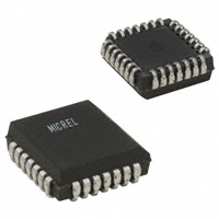
■ Available in 28-pin PLCC package
BLOCK DIAGRAM
D0
Q0
D0
Q0
D1
Q1
D1
Q1
D2
Q2
D2
Q2
D3
Q3
D3
Q3
D4
Q4
D4
Q4
PIN NAMES
Pin
VBB
M9999-032006
hbwhelp@micrel.com or (408) 955-1690
SY10E116
SY100E116
Function
D0, D0-D4, D4
Differential Input Pairs
Q0, Q0-Q4, Q4
Differential Output Pairs
VBB
Reference Voltage Output
VCCO
VCC to Output
Rev.: H
1
Amendment: /0
Issue Date: March 2006
�SY10E116
SY100E116
Micrel, Inc.
Ordering Information(1)
VCCO
Q4
VCCO
Q4
D4
D3
25
D4
PACKAGE/ORDERING INFORMATION
24 23 22 21 20 19
D3
26
18
D2
27
17
D2
VEE
VBB
28
16
15
PLCC
TOP VIEW
J28-1
1
2
14
Q3
Part Number
Package
Type
Operating
Range
Package
Marking
Lead
Finish
SY10E116JI
J28-1
Industrial
SY10E116JI
Sn-Pb
Q3
SY10E116JITR(2)
J28-1
Industrial
SY10E116JI
Sn-Pb
VCC
SY100E116JI
J28-1
Industrial
SY100E116JI
Sn-Pb
Q2
Q2
SY100E116JITR(2)
J28-1
Industrial
SY100E116JI
Sn-Pb
J28-1
Commercial
SY10E116JC
Sn-Pb
SY10E116JCTR(2)
J28-1
Commercial
SY10E116JC
Sn-Pb
SY100E116JC
J28-1
Commercial
SY100E116JC
Sn-Pb
SY100E116JCTR(2)
J28-1
Commercial
SY100E116JC
Sn-Pb
SY10E116JY(3)
J28-1
Industrial
SY10E116JY with
Pb-Free bar-line indicator
Matte-Sn
SY10E116JYTR(2, 3)
J28-1
Industrial
SY10E116JY with
Pb-Free bar-line indicator
Matte-Sn
SY100E116JY(3)
J28-1
Industrial
SY100E116JY with
Pb-Free bar-line indicator
Matte-Sn
SY100E116JYTR(2, 3)
J28-1
Industrial
SY100E116JY with
Pb-Free bar-line indicator
Matte-Sn
7
8
9
10 11
Q1
6
VCCO
5
Q0
SY10E116JC
Q1
Q0
VCCO
12
VCCO
13
4
D1
3
D0
D1
D0
28-Pin PLCC (J28-1)
Notes:
1. Contact factory for die availability. Dice are guaranteed at TA = 25°C, DC Electricals only.
2. Tape and Reel.
3. Pb-Free package is recommended for new designs.
M9999-032006
hbwhelp@micrel.com or (408) 955-1690
2
�SY10E116
SY100E116
Micrel, Inc.
LOGIC EQUATION
Qn = Dn
DC ELECTRICAL CHARACTERISTICS
VEE = VEE(Min.) to VEE(Max.); VCC = VCCO = GND
TA = –40°C
Symbol
VBB
Parameter
Output Reference
Voltage
10E
100E
TA = 0°C
TA = +25°C
TA = +85°C
Min. Typ.
Max.
Min.
Typ.
Max.
Min.
Typ.
Max.
Min.
Typ.
Max.
–1.43
–1.43
—
—
–1.30
–1.26
–1.38
–1.38
—
—
–1.27
–1.26
–1.35
–1.38
—
—
–1.25
–1.26
–1.31
–1.38
—
—
–1.19
–1.26
Unit
V
µA
IIH
Input HIGH Current
—
—
200
—
—
200
—
—
200
—
—
200
IEE
Power Supply Current
10E
100E
—
—
29
29
35
35
—
—
29
29
35
35
—
—
29
29
35
35
—
—
29
33
35
40
150
—
—
150
—
—
150
—
—
150
—
—
mV
–2.0
—
–0.6
–2.0
—
–0.6
–2.0
—
–0.6
–2.0
—
–0.6
V
VPP (DC)
VCMR
Input Sensitivity(1)
Common Mode Range
(2)
mA
Notes:
1. VPP is the minimum differential input voltage required to assure full ECL levels are present at the outputs.
2. VCMR is referenced to the most positive side of the differential input signal. Normal operation is obtained when the "HIGH" input is within the VCMR range
and the input swing is greater than VPP (min.) and
很抱歉,暂时无法提供与“SY100E116JI”相匹配的价格&库存,您可以联系我们找货
免费人工找货