NOT RECOMMENDED FOR NEW DESIGNS
Micrel, Inc.
SY10E451
SY100E451
SY10E451
6-BIT REGISTER
DIFFERENTIAL DATA CLOCK
FEATURES
DESCRIPTION
■
■
■
■
■
■
1100MHz min. toggle frequency
Extended 100E VEE range of –4.2V to –5.5V
Differential inputs: data and clock
VBB output for single-ended use
Asynchronous Master Reset
Fully compatible with industry standard 10KH,
100K ECL levels
■ Internal 75KΩ input pulldown resistors
■ Fully compatible with Motorola MC10E/100E451
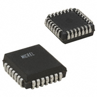
■ Available in 28-pin PLCC package
The SY10/100E451 offer six D-type flip-flops with singleended outputs and differential data and clock inputs,
designed for use in new, high-performance ECL systems.
The registers are triggered by the rising edge of the CLK
input.
A logic HIGH on the Master Reset (MR) input resets all
outputs to a logic LOW. The VBB output is provided for use
as a reference voltage for single-ended reception of ECL
signals to that device only. When used for this purpose, it
is recommended that VBB is decoupled to VCC via a 0.01µF
capacitor.
BLOCK DIAGRAM
PIN NAMES
Pin
D0
/D0
Q0
D
R
D1
/D1
Q1
D
R
D2
/D2
Q2
D
R
D3
/D3
SY100E451
Function
D0–D5
+ Data Input
/D0–/D5
– Data Input
CLK
+ Clock Input
/CLK
– Clock Input
Q0–Q5
Data Outputs
MR
Master Reset Input
VBB
VBB Output
VCCO
VCC to Output
Q3
D
R
D4
/D4
Q4
D
R
D5
/D5
Q5
D
R
CLK
/CLK
MR
VBB
M9999-032206
hbwhelp@micrel.com or (408) 955-1690
Rev.: G
1
Amendment: /0
Issue Date: March 2006
�SY10E451
SY100E451
Micrel, Inc.
PACKAGE/ORDERING INFORMATION
VCCO
/D3
D3
/D5
D5
/D4
D4
Ordering Information(1)
25 24 23 22 21 20 19
17
28
1
Q5
Q4
Package
Type
Operating
Range
Package
Marking
Lead
Finish
SY10E451JI
J28-1
Industrial
SY10E451JI
Sn-Pb
SY10E451JITR(2)
J28-1
Industrial
SY10E451JI
Sn-Pb
SY100E451JI
J28-1
Industrial
SY100E451JI
Sn-Pb
J28-1
Industrial
SY100E451JI
Sn-Pb
J28-1
Commercial
SY10E451JC
Sn-Pb
15
VCC
Q3
SY100E451JITR
16
TOP VIEW
PLCC
J28-1
(2)
14
VCCO
SY10E451JC
3
13
SY10E451JCTR(2)
J28-1
Commercial
SY10E451JC
Sn-Pb
4
12
Q2
Q1
SY100E451JC
J28-1
Commercial
SY100E451JC
Sn-Pb
SY100E451JCTR(2)
J28-1
Commercial
SY100E451JC
Sn-Pb
SY10E451JY(3)
J28-1
Industiral
SY10E451JY with
Pb-Free bar-line indicator
Matte-Sn
SY10E451JYTR(2, 3)
J28-1
Industrial
SY10E451JY with
Pb-Free bar-line indicator
Matte-Sn
SY100E451JY(3)
J28-1
Industrial
SY100E451JY with
Pb-Free bar-line indicator
Matte-Sn
SY100E451JYTR(2, 3)
J28-1
Industrial
SY100E451JY with
Pb-Free bar-line indicator
Matte-Sn
6
7
8
9
10 11
VCCO
Q0
/D0
5
D2
2
/D2
MR
NC
D0
18
/D1
/CLK
VEE
26
27
D1
CLK
VBB
Part Number
28-Pin PLCC (J28-1)
Notes:
1. Contact factory for die availability. Dice are guaranteed at TA = 25°C, DC Electricals only.
2. Tape and Reel.
3. Pb-Free package is recommended for new designs.
M9999-032206
hbwhelp@micrel.com or (408) 955-1690
2
�SY10E451
SY100E451
Micrel, Inc.
DC ELECTRICAL CHARACTERISTICS
VEE = VEE (Min.) to VEE (Max.); VCC = VCCO = GND
TA = –40°C
Symbol
Parameter
Min.
VBB
Output Reference 10E
Voltage
100E
IIH
Input HIGH Current
IEE
Power Supply
Current
VCMR
Common Mode Range(1)
Typ.
Max.
10E
100E
TA = 0°C
TA = 25°C
Max.
Min.
Typ.
TA = +85°C
Min.
Typ.
–1.38
–1.38
—
—
—
—
150
—
—
150
—
—
84
84
101
101
—
—
84
84
–2.0
—
–0.4
–2.0
—
–1.27 –1.35
–1.26 –1.38
—
—
Max.
Min.
Typ.
Max.
Unit
—
—
–1.19
–1.26
V
—
—
150
µA
101
101
—
—
84
97
101
116
mA
–0.4
–2.0
—
–0.4
V
–1.25 –1.31
–1.26 –1.38
Note:
1. VCMR is referenced to the most psitive side of the differential input signal. Normal operation is obtained when the “HIGH” input is within the VCMR range
and the input swing is greater than VPP (min) and < 1V.
AC ELECTRICAL CHARACTERISTICS
VEE = VEE (Min.) to VEE (Max.); VCC = VCCO = GND
TA = –40°C
Symbol
Parameter
Min.
Typ.
Max.
TA = 0°C
TA = 25°C
TA = +85°C
Min.
Typ.
Max.
Min.
Typ.
Max.
Min.
Typ.
Max.
Unit
MHz
fMAX
Max. Toggle Frequency
1100
1400
—
1100
1400
—
1100
1400
—
tPD
Propagation Delay to
Output
CLK (Diff)
CLK (SE)
MR
475
425
425
650
650
600
800
850
850
475
425
425
650
650
600
800
850
850
475
425
425
650
650
600
800
850
850
ps
tS
Set-up Time
D
150
–100
—
150
–100
—
150
–100
—
ps
tH
Hold Time
D
250
100
—
250
100
—
250
100
—
ps
VPP (AC)
Minimum Input Swing(1)
150
—
—
150
—
—
150
—
—
mV
tRR
Reset Recovery Time
750
600
—
750
600
—
750
600
—
ps
tPW
Minimum Pulse Width
CLK, MR
400
—
—
400
—
—
400
—
—
ps
tskew
Within-Device Skew(2)
—
100
—
—
100
—
—
100
—
ps
tr
tf
Rise/Fall Time
20% to 80%
275
450
800
275
450
800
275
450
800
ps
Notes:
1. Minimum input voltage for which AC parameters are guaranteed.
2. Within-device skew is defined as identical transitions on similar paths through a device.
M9999-032206
hbwhelp@micrel.com or (408) 955-1690
3
�SY10E451
SY100E451
Micrel, Inc.
28-PIN PLCC (J28-1)
Rev. 03
MICREL, INC. 2180 FORTUNE DRIVE SAN JOSE, CA 95131
TEL
+ 1 (408) 944-0800
FAX
+ 1 (408) 474-1000
WEB
USA
http://www.micrel.com
The information furnished by Micrel in this data sheet is believed to be accurate and reliable. However, no responsibility is assumed by Micrel for its use.
Micrel reserves the right to change circuitry and specifications at any time without notification to the customer.
Micrel Products are not designed or authorized for use as components in life support appliances, devices or systems where malfunction of a product can
reasonably be expected to result in personal injury. Life support devices or systems are devices or systems that (a) are intended for surgical implant into
the body or (b) support or sustain life, and whose failure to perform can be reasonably expected to result in a significant injury to the user. A Purchaser’s
use or sale of Micrel Products for use in life support appliances, devices or systems is at Purchaser’s own risk and Purchaser agrees to fully indemnify
Micrel for any damages resulting from such use or sale.
© 2006 Micrel, Incorporated.
M9999-032206
hbwhelp@micrel.com or (408) 955-1690
4
�
很抱歉,暂时无法提供与“SY100E451JC”相匹配的价格&库存,您可以联系我们找货
免费人工找货