SY100S351
FINAL
HEX D FLIP-FLOP
FEATURES
Q1
Q1
Q0
D0
Q0
VEES
PIN CONFIGURATIONS
D1
11 10 9 8 7 6 5
D2
CPa
12
13
14
15
16
17
CPb
18
D3
VEE
VEES
MR
BLOCK DIAGRAM
Top View
PLCC
J28-1
4
3
2
1
28
27
Q2
26
Q3
Q2
VCCA
VCC
VCC
Q3
D
Q4
R
Q
D4
D5
Q4
D
Q
Q3
E
Q
Q3
Q
Q2
Q
Q2
D
Q
Q1
E
R Q
Q1
D
Q
Q0
E
R Q
Q0
Q5
Q5
Q4
D2
D
E
D1
D0
R
R
1
24 23 22 21 20 19
18
D1
2
3
17
16
D0
Q0
15
14
Q0
Q1
13
7 8 9 10 11 12
Q1
Top View
Flatpack
F24-1
4
5
6
Q3
Q4
Rev.: G
1
D2
Q
D3
Q5
CPa
MR
VEE
Q
Q2
Q2
R
CPb
Q5
VCCA
E
E
D3
Q
Q3
VCC
D
Q4
D5
CPb
CPa
MR
D4
Q5
Q4
19 20 21 22 23 24 25
VEES
■
■
■
■
■
The SY100S351 offers six D-type, edge-triggered,
master/slave flip-flops with differential outputs, and is
designed for use in high-performance ECL systems. The
flip-flops are controlled by the signal from the logical OR
operation on a pair of common clock signals (CPa, CPb).
Data enters the master when both CPa and CPb are LOW
and transfers to the slave when either CPa or CPb (or both)
go to a logic HIGH. The Master Reset (MR) input overrides
all other inputs and takes the Q outputs to a logic LOW. The
inputs on this device have 75KΩ pull-down resistors.
D5
Q5
■
Max. toggle frequency of 700MHz
Clock to Q max. of 1200ps
IEE min. of –98mA
Industry standard 100K ECL levels
Extended supply voltage option:
VEE = –4.2V to –5.5V
Voltage and temperature compensation for improved
noise immunity
Internal 75KΩ input pull-down resistors
50% faster than Fairchild 300K
Better than 20% lower power than Fairchild
Function and pinout compatible with Fairchild F100K
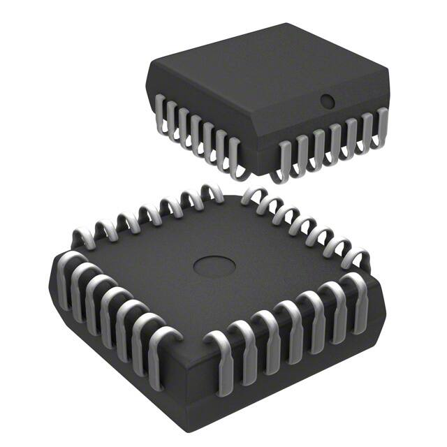
Available in 24-pin CERPACK and 28-pin PLCC
packages
D4
■
■
■
■
■
DESCRIPTION
Amendment: /0
Issue Date: July, 1999
�SY100S351
Micrel
PIN NAMES
Pin
Function
D0 — D5
Data Inputs
CPa, CPb
Common Clock Inputs
MR
Asynchronous Master Reset Input
Q0 — Q5
Data Outputs
Q0 — Q5
Complementary Data Outputs
VEES
VEE Substrate
VCCA
VCCO for ECL Outputs
TRUTH TABLES
Synchronous Operation(1)
Asynchronous Operation(1)
Inputs
Inputs
Outputs
Dn
CPa
CPb
MR
Qn (t+1)
X
X
X
H
L
NOTE:
1. H = High Voltage Level
L = Low Voltage Level
X = Don't Care
t = Time before CP Positive Transition
t+1 = Time after CP Positive Transition
u = LOW-to-HIGH Transition
Outputs
Dn
CPa
CPb
MR
Qn (t+1)
L
u
L
L
L
H
u
L
L
H
L
L
u
L
L
H
L
u
L
H
X
H
u
L
Qn(t)
X
u
H
L
Qn(t)
X
L
L
L
Qn(t)
Unit
DC ELECTRICAL CHARACTERISTICS
VEE = –4.2V to –5.5V unless otherwise specified; VCC = VCCA = GND
Symbol
IIH
IEE
Parameter
Input HIGH Current
MR
D0 – D5
CPa, CPb
Power Supply Current
Min.
Typ.
Max.
—
—
—
—
—
—
270
200
300
–98
–71
–49
2
Condition
µA
VIN = VIH (Max.)
mA
Inputs Open
�SY100S351
Micrel
AC ELECTRICAL CHARACTERISTICS
CERPACK
VEE = –4.2V to –5.5V unless otherwise specified; VCC = VCCA = GND
TA = 0°C
Symbol
Parameter
TA = +25°C
TA = +85°C
Min.
Max.
Min.
Max.
Min.
Max.
Unit
fMAX
Toggle Frequency
700
—
700
—
700
—
MHz
tPLH
tPHL
Propagation Delay
CPa, CPb to Output
—
1200
—
1200
—
1200
ps
tPLH
tPHL
Propagation Delay
MR to Output
—
1200
—
1200
—
1200
ps
tTLH
tTHL
Transition Time
20% to 80%, 80% to 20%
300
900
300
900
300
900
ps
tS
Set-up Time
D0–D5
MR (Release Time)
500
1000
—
—
500
1000
—
—
500
1000
—
—
tH
Hold Time, D0–D5
550
—
550
—
550
—
ps
tPW (H)
Pulse Width HIGH
CPa, CPb, MR
1000
—
1000
—
1000
—
ps
Condition
ps
PLCC
VEE = –4.2V to –5.5V unless otherwise specified; VCC = VCCA = GND
TA = 0°C
Symbol
Parameter
TA = +25°C
TA = +85°C
Min.
Max.
Min.
Max.
Min.
Max.
Unit
fMAX
Toggle Frequency
700
—
700
—
700
—
MHz
tPLH
tPHL
Propagation Delay
CPa, CPb to Output
—
1200
—
1200
—
1200
ps
tPLH
tPHL
Propagation Delay
MR to Output
—
1200
—
1200
—
1200
ps
tTLH
tTHL
Transition Time
20% to 80%, 80% to 20%
300
900
300
900
300
900
ps
tS
Set-up Time
D0–D5
MR (Release Time)
500
1000
—
—
500
1000
—
—
500
1000
—
—
tH
Hold Time, D0–D5
550
—
550
—
550
—
ps
tPW (H)
Pulse Width HIGH
CPa, CPb, MR
1000
—
1000
—
1000
—
ps
ps
3
Condition
�SY100S351
Micrel
TIMING DIAGRAMS
DATA
0.7 ± 0.1 ns
0.7 ± 0.1 ns
–0.95V
80%
50%
20%
CLOCK
–1.69V
1/fmax
tPHL
tpw (H)
tPLH
OUTPUT
50%
tPHL
tPLH
OUTPUT
tTLH
tTHL
Propagation Delay (Clock) and Transition Times
NOTE:
VEE = –4.2V to –5.5V unless otherwise specified; VCC = VCCA = GND
0.7 ± 0.1 ns
0.7 ± 0.1 ns
–0.95V
80%
50%
20%
MR
–1.69V
tS (RELEASE TIME)
tpw (H)
CLOCK
50%
tPHL
tPLH
OUTPUT
50%
tPLH
tPHL
80%
50%
20%
OUTPUT
Propagation Delay (Resets)
4
�SY100S351
Micrel
TIMING DIAGRAMS
–0.95V
DATA
50%
–1.69V
tH
tS
–0.95V
CLOCK
50%
–1.69V
Data Set-up and Hold Time
NOTES:
1. VEE = –4.2V to –5.5V unless otherwise specified; VCC = VCCA = GND
2. tS is the minimum time before the transition of the clock that information
must be present at the data input.
3. tH is the minimum time after the transition of the clock that information must
remain unchanged at the data input.
PRODUCT ORDERING CODE
Ordering
Code
5
Package
Type
Operating
Range
SY100S351FC
F24-1
Commercial
SY100S351JC
J28-1
Commercial
SY100S351JCTR
J28-1
Commercial
�SY100S351
Micrel
24 LEAD CERPACK (F24-1)
Rev. 03
6
�SY100S351
Micrel
28 LEAD PLCC (J28-1)
Rev. 03
MICREL-SYNERGY
TEL
3250 SCOTT BOULEVARD
+ 1 (408) 980-9191
FAX
SANTA CLARA
+ 1 (408) 914-7878
WEB
CA 95054 USA
http://www.micrel.com
This information is believed to be accurate and reliable, however no responsibility is assumed by Micrel for its use nor for any infringement of patents or
other rights of third parties resulting from its use. No license is granted by implication or otherwise under any patent or patent right of Micrel Inc.
© 2000 Micrel Incorporated
7
�
很抱歉,暂时无法提供与“SY100S351FC”相匹配的价格&库存,您可以联系我们找货
免费人工找货