SY84113BU
Low Power 2.5V 1.25Gbps Limiting Post
Amplifier with Ultra Wide LOS Range
General Description
Features
The SY84113BU low power limiting post amplifier is
designed for use in fiber-optic optical modules for
multirate applications up to 1.25Gbps. The device
connects to a typical transimpedance amplifier (TIA) and
can produce output signals to CML-level waveforms.
Intended for the GbE and Fibre Channel applications,
the SY84113BU offers a wide loss-of-signal (LOS)
range. It is able to detect input signals for as low as
5mVpp and as high as 100mVpp. The SY84113BU is
intended to be used in AC-coupled input applications.
The SY84113BU generates a LOS open-collector TTL
output. A programmable LOS level set pin (LOSLVL) sets
the sensitivity of the input amplitude detection. LOS
asserts high if the input amplitude falls below the
threshold set by LOSLVL and de-asserts low otherwise.
The enable input (/EN) de-asserts the true output signal
without removing the input signal. The LOS output can
be fed back to the /EN input to implement the squelch
function that maintains output stability under an LOS
condition.
The SY84113BU operates on a single 2.5V power
supply and offers ultra-low power consumption. This
device is perfectly suited to meet the stringent power
requirements of the CSFP/SFP/SFF optical modules.
All support documentation can be found on Micrel’s
website at: www.micrel.com.
• Ultra-wide loss-of-signal (LOS) range (5mVpp to
100mVpp)
• Single 2.5V power supply
• Ultra-low power consumption (55mW typical)
• 125Mbps to 1.25 Gbps operation
• Low-noise CML data outputs
• TTL /EN input
• Programmable LOS level (LOSLVL)
• Internal 50Ω termination
• Available in a tiny 3mm × 3mm QFN package
• Extensive temperature range (–40°C to +95°C)
Applications
• Gigabit Ethernet
• Fibre Channel
• GEPON
Markets
• Datacom/telecom
• Compact SFP/SFF optical transceiver
• SFP/SFF optical transceiver
_________________________________________________________________________________________________________
Typical Application
Micrel Inc. • 2180 Fortune Drive • San Jose, CA 95131 • USA • tel +1 (408) 944-0800 • fax + 1 (408) 474-1000 • http://www.micrel.com
August 11, 2015
Revision 2.0
hbwhelp@micrel.com or (408) 955-1690
�Micrel, Inc.
SY84113BU
Ordering Information
Part Number
Package Type
Operating Range
Package Marking
Lead Finish
QFN-16
Industrial
113B with Pb-Free Bar-Line Indicator
NiPdAu Pb-Free
QFN-16
Industrial
113B with Pb-Free Bar-Line Indicator
NiPdAu Pb-Free
SY84113BUMG
(1)
SY84113BUMGTR
Notes:
1. Tape and Reel.
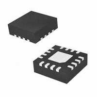
Pin Configuration
16-Pin (3mm × 3mm) QFN-16
Pin Description
Pin Number
Pin Name
Type
15
/EN
TTL Input
/Enable: This input enables the outputs when LOW. Internally
connected to a 25kΩ pull-up resistor and will default to a logic HIGH
state if left open.
1, 4
DIN, /DIN
Data Input
Differential data inputs. Each input is internally terminated to the VREF
pin by a 50Ω resistor.
6
VREF
14
LOSLVL
DC Input
2, 3, 10,
11, ePad
GND
Ground
7
LOS
Open-Collector
TTL Output
Loss-of-signal: asserts high when the data input amplitude falls below
the threshold set by LOSLVL.
12, 9
/DOUT, DOUT
CML Output
Differential data outputs. Unused output should be terminated 50Ω to
VCC.
5, 8, 13, 16
VCC
Positive Rail
Positive power supply. . Bypass with a 0.1uF || 0.01uF low-ESR
capacitor as close to VCC pin as possible.
August 11, 2015
Pin Function
Reference Voltage: Place 0.1uF capacitor to Vcc to help stabilize
LOSLVL.
Loss-of-Signal Level Set. A resistor from this pin to VCC sets the
threshold for the data input amplitude at which LOS will be asserted.
Device Ground. Exposed pad (ePad) must be connected to PCB ground
plane.
2
Revision 2.0
hbwhelp@micrel.com or (408) 955-1690
�Micrel, Inc.
SY84113BU
Absolute Maximum Ratings(2)
Operating Ratings(3)
Supply Voltage (VCC) ....................................... 0V to +4.0V
Input Voltage (DIN, /DIN) .......................................0 to VCC
Output Current (IOUT) ............................................... ±25mA
EN Voltage .............................................................0 to VCC
VREF Current ......................................... –800µA to +500µA
LOSLVL Voltage ................................................. VREF to VCC
Lead Temperature (soldering, 20s) .......................... 260°C
Storage Temperature (Ts) ....................... –65°C to +150°C
Supply Voltage (VCC) ...................... +2.375 to +2.625V
Ambient Temperature (TA).................. –40°C to +95°C
Junction Temperature (TJ) ................ –40°C to +120°C
(4)
Package Thermal Resistance
(θJA) Still-Air ................................................ 60°C/W
(ψJB) ............................................................ 33°C/W
DC Electrical Characteristics
VCC = 2.5 ±5%; TA = –40°C to +95°C, typical values at VCC = 2.5V, TA = 25°C.
Symbol
Parameter
Condition
Min.
Typ.
ICC
Power Supply Current
Outputs terminated 50Ω to Vcc
LOSLVL
LOSLVL Voltage
VREF
VOH
DOUT, /DOUT
HIGH Voltage
VCC – 0.020
VOL
DOUT, /DOUT
LOW Voltage
VCC – 0.475
VREF
Reference Voltage
Z0
Single-Ended
Output Impedance
40
50
60
Ω
ZI
Single-Ended
Input Impedance
40
50
60
Ω
Min.
Typ.
Max.
Units
Vcc
V
22
Max.
Units
35
mA
VCC
V
VCC – 0.005
VCC
V
VCC – 0.400
VCC – 0.350
V
Vcc – 0.6
V
TTL DC Electrical Characteristics
VCC = 2.5 ±5%; TA = –40°C to +95°C, typical values at VCC = 2.5V, TA = 25°C.
Symbol
Parameter
Condition
VIH
/EN Input HIGH Voltage
VIL
/EN Input LOW Voltage
IIH
/EN Input HIGH Current
VIN = VCC
IIL
/EN Input LOW Current
VIN = 0.5V
2.0
VOH
LOS Output HIGH Level
Vcc = 2.5V. IOH < 50uA
VOL
LOS Output LOW Level
IOL = 2mA
0.8
V
20
µA
–0.3
mA
2
V
0.5
V
Notes:
2. Permanent device damage may occur if absolute maximum ratings are exceeded. This is a stress rating only and functional operation is not
implied at conditions other than those detailed in the operational sections of this data sheet. Exposure to absolute maximum ratings conditions
for extended periods may affect device reliability.
3. The datasheet limits are not guaranteed if the device is operated beyond the operating ratings.
4. Package Thermal Resistance assumes exposed pad is soldered (or equivalent) to the devices most negative potential on the PCB. ψJB uses a
4-layer and θJA in still air unless otherwise stated.
August 11, 2015
3
Revision 2.0
hbwhelp@micrel.com or (408) 955-1690
�Micrel, Inc.
SY84113BU
AC Electrical Characteristics
VCC = 2.5 ±5%; TA = –40°C to +95°C, typical values at VCC = 2.5V, TA = 25°C.; RLoad = 50Ω to VCC;
Symbol
tr , tf
tJITTER
Parameter
Typ.
Max.
Units
Note 5
150
260
ps
Deterministic
Note 6
15
Random
Note 7
Output Rise/Fall Time
(20% to 80%)
VID
Differential Input Voltage Swing
VOD
Differential Output Voltage Swing
Condition
Min.
psPP
5
5
Note 5
700
800
psRMS
1800
mVPP
950
mVPP
TOFF
LOS Release Time
Note 10
2
10
µS
TON
LOS Assert Time
Note 10
2
10
µS
LOSAL
Low LOS Assert Level
RLOSLVL = 10kΩ
(8)
LOSDL
Low LOS De-assert Level
RLOSLVL = 10kΩ
(8)
HYSL
Low LOS Hysteresis
RLOSLVL = 10kΩ
(8)
LOSAM
LOSDM
Medium LOS Assert Level
Medium LOS De-assert Level
RLOSLVL = 5kΩ
(8)
RLOSLVL = 5kΩ
(8)
(9)
HYSM
Medium LOS Hysteresis
RLOSLVL = 5kΩ
LOSAH
High LOS Assert Level
RLOSLVL = 100Ω
(8)
LOSDH
High LOS De-assert Level
RLOSLVL = 100Ω
(8)
RLOSLVL = 100Ω
(9)
3.9
mVPP
5.6
2
3.1
7
9.2
mVPP
4.5
mVPP
13.6
16
2
3.4
4.5
60
73
2
dB
mVPP
dB
mVPP
103
130
3.0
4.5
mVPP
HYSH
High LOS Hysteresis
B-3dB
3dB Bandwidth
850
MHz
AV(Diff)
Differential Voltage Gain
38
dB
S21
Single-Ended Small-Signal Gain
32
dB
26
dB
Notes:
5. Amplifier in limiting mode. Input is a 200MHz square wave.
6. Deterministic jitter measured using 1.250 Gbps K28.5 pattern, VID = 60mVPP.
7. Random jitter measured using 1.250Gbps K28.7 pattern, VID = 60mVPP.
8. See “Typical Operating Characteristics” for a graph showing how to choose a particular RLOSLVL for a particular LOS assert and its associated
de-assert amplitude.
9. This specification defines electrical hysteresis as 20log (LOS De-Assert/LOS Assert). The ratio between optical hysteresis and electrical
hysteresis is found to vary between 1.5 and 2 depending upon the level of received optical power and ROSA characteristics. Based on that
ratio, the optical hysteresis corresponding to the electrical hysteresis range 2dB-4.5 dB, shown in the AC characteristics table, will be 1dB-3dB
Optical Hysteresis.
10. In real world applications, the LOS Release/Assert time can be strongly influenced by the RC time constant of the AC-coupling cap and the
50Ω input termination. To keep this time low, use a decoupling cap with the lowest value that is allowed by the data rate and the number of
consecutive identical bits in the application (typical values are in the range of 0.001µF to 1.0µF).
August 11, 2015
4
Revision 2.0
hbwhelp@micrel.com or (408) 955-1690
�Micrel, Inc.
SY84113BU
Typical Functional Characteristics
VCC = 2.5 ±5%; TA = –40°C to +95°C, typical values at VCC = 2.5V, TA = 25°C.; RLoad = 50Ω to VCC.
Typical Operating Characteristics
VCC = 2.5 ±5%; TA = –40°C to +95°C, typical values at VCC = 2.5V, TA = 25°C.; RLoad = 50Ω to VCC.
LOS Assert/De-Assert Levels
LOS Hysteresis
1000
6
Hysteresis (dB)
Amplitude (mV)
5
100
10
4
3
2
1
1
0.1
1
10
0.1
LOSLVL Resistor (KOhm)
August 11, 2015
1
10
LOSLVL Resistor (KOhm)
5
Revision 2.0
hbwhelp@micrel.com or (408) 955-1690
�Micrel, Inc.
SY84113BU
Functional Block Diagram
August 11, 2015
6
Revision 2.0
hbwhelp@micrel.com or (408) 955-1690
�Micrel, Inc.
SY84113BU
Functional Description
The SY84113BU is a high-sensitivity limiting post
amplifier that operates from a single +2.5V power supply
over temperatures from –40°C to +85°C. Signals with
data rates up to 1.25Gbps, and as small as 5mVpp, can
be amplified. Figure 1 shows the allowed input voltage
swing. The SY84113BU generates a LOS output signal
that can be fed back to /EN for output stability in the
absence of a signal at the input. LOSLVL sets the
sensitivity of the input amplitude detection. SY84113BU
offers ultra wide LOS detection range. This allows the
device to be used in multiple AC-coupled applications.
Hysteresis
The SY84113BU provides typically 3dB LOS electrical
hysteresis, which is defined as 20log (VINLOS-Assert /
VINLOS-De-Assert). Because the relationship between the
voltage out of the ROSA to optical power at its input is
linear, the optical hysteresis will be typically half of the
electrical hysteresis reported in the datasheet, but in
practice the ratio between electrical and optical
hysteresis is found to be within the range 1.5 - 1.8. Thus
3dB electrical hysteresis will correspond to an optical
hysteresis within the range 1.7dB - 2dB.
Input Amplifier/Buffer
Figure 2 shows a simplified schematic of the input
stage. The high-sensitivity of the input amplifier can
detect and amplify AC-coupled signals as small as
5mVpp to full CML output level. The input stage also can
allow signals as large as 1800mVpp. Input signals are
amplified with a typically 38dB differential voltage gain
until they reach the limiting mode of the amplifier.
SY84113BU outputs in standard 400mV CML output
levels.
Output Buffer
The SY84113BU’s CML output buffer is designed to
drive 50Ω lines and is internally terminated with 50Ω to
VCC. Figure 3 shows a schematic of the output stage.
Loss-of-Signal (LOS)
The SY84113BU generates a chatter-free LOSs-ofsignal (LOS) open-collector TTL output as shown in
Figure 4. LOS is used to determine that the input
amplitude is too small to be considered as a valid input.
LOS asserts high if the input amplitude falls below the
threshold set by LOSLVL and de-asserts low otherwise.
LOS can be fed back to the enable (/EN) input to
maintain output stability under a LOSs of signal
condition. /EN de-asserts low the true output signal
without removing the input signals. Typically, 3dB LOS
hysteresis is provided to prevent chattering.
LOS Level Set
A programmable LOS level set pin (LOSLVL) sets the
threshold of the input amplitude detection. Connecting
an external resistor between VCC and LOSLVL sets the
voltage at LOSLVL. This voltage ranges from VCC to
VREF. The external resistor creates a voltage divider
between VCC and VREF, as shown in Figure 5.
August 11, 2015
7
Revision 2.0
hbwhelp@micrel.com or (408) 955-1690
�Micrel, Inc.
SY84113BU
Figure 1. VIS and VID Definition
Figure 2. Input Structure
Figure 3. Output Structure
Figure 4. LOS Output Structure
Figure 5. LOSLVL Setting Circuit
Note: Recommended value for RLOSLVL is 15kΩ or less.
August 11, 2015
8
Revision 2.0
hbwhelp@micrel.com or (408) 955-1690
�Micrel, Inc.
SY84113BU
Package Information and Recommended Land Pattern(11)
16-Pin (3mm × 3mm) QFN (QFN-16)
Note:
11. Package information is correct as of the publication date. For updates and most current information, go to www.micrel.com.
August 11, 2015
9
Revision 2.0
hbwhelp@micrel.com or (408) 955-1690
�Micrel, Inc.
SY84113BU
Package Information and Recommended Land Pattern(11) (Continued)
August 11, 2015
10
Revision 2.0
hbwhelp@micrel.com or (408) 955-1690
�Micrel, Inc.
SY84113BU
MICREL, INC. 2180 FORTUNE DRIVE SAN JOSE, CA 95131 USA
TEL +1 (408) 944-0800 FAX +1 (408) 474-1000 WEB http://www.micrel.com
Micrel, Inc. is a leading global manufacturer of IC solutions for the worldwide high performance linear and power, LAN, and timing &
communications markets. The Company’s products include advanced mixed-signal, analog & power semiconductors; high-performance
communication, clock management, MEMs-based clock oscillators & crystal-less clock generators, Ethernet switches, and physical layer
transceiver ICs. Company customers include leading manufacturers of enterprise, consumer, industrial, mobile, telecommunications, automotive,
and computer products. Corporation headquarters and state-of-the-art wafer fabrication facilities are located in San Jose, CA, with regional sales
and support offices and advanced technology design centers situated throughout the Americas, Europe, and Asia. Additionally, the Company
maintains an extensive network of distributors and reps worldwide.
Micrel makes no representations or warranties with respect to the accuracy or completeness of the information furnished in this datasheet. This
information is not intended as a warranty and Micrel does not assume responsibility for its use. Micrel reserves the right to change circuitry,
specifications and descriptions at any time without notice. No license, whether express, implied, arising by estoppel or otherwise, to any
intellectual property rights is granted by this document. Except as provided in Micrel’s terms and conditions of sale for such products, Micrel
assumes no liability whatsoever, and Micrel disclaims any express or implied warranty relating to the sale and/or use of Micrel products including
liability or warranties relating to fitness for a particular purpose, merchantability, or infringement of any patent, copyright, or other intellectual
property right.
Micrel Products are not designed or authorized for use as components in life support appliances, devices or systems where malfunction of a
product can reasonably be expected to result in personal injury. Life support devices or systems are devices or systems that (a) are intended for
surgical implant into the body or (b) support or sustain life, and whose failure to perform can be reasonably expected to result in a significant injury
to the user. A Purchaser’s use or sale of Micrel Products for use in life support appliances, devices or systems is a Purchaser’s own risk and
Purchaser agrees to fully indemnify Micrel for any damages resulting from such use or sale.
© 2010 Micrel, Incorporated.
August 11, 2015
11
Revision 2.0
hbwhelp@micrel.com or (408) 955-1690
�


 工商网监
湘ICP备2023018690号
工商网监
湘ICP备2023018690号
