SY84403BL
Ultra Small 3.3V 4.25Gbps CML Low-Power
Limiting Post Amplifier with TTL LOS
General Description
Features
The SY84403BL is the industry’s smallest limiting post
amplifier ideal for compact copper and fiber optic
module applications. The device connects to typical
transimpedance amplifiers (TIAs). The linear signal
output from TIAs can contain significant amounts of
noise and may vary in amplitude over time. The
SY84403BL quantizes these signals and outputs
typically 800mVPP voltage-limited waveforms.
®
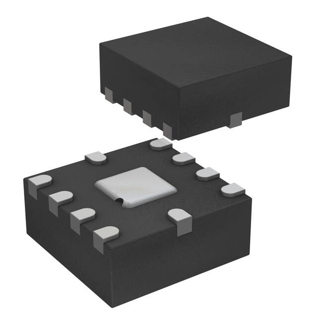
The SY84403BL comes in a tiny 10-pin 2x2 MLF
package, which is unparalleled in the industry. It offers
space savings of 55% or more over typical post amps.
It operates from a single +3.3V ±10% power supply,
over an industrial temperature range of –40°C to
+85°C. With its wide bandwidth and high gain, signals
with data rates up to 4.25Gbps and as small as
10mVPP can be amplified to drive devices with CML
inputs or AC-coupled PECL inputs.
The SY84403BL incorporates a loss-of-signal (LOS)
open-collector TTL output with internal 4.75kΩ pull-up
resistor. A programmable loss-of-signal level set pin
(LOSLVL) sets the sensitivity of the input amplitude
detection. LOS asserts high if the input amplitude falls
below the threshold set by LOSLVL and de-asserts
low otherwise. LOS can be fed back to the enable bar
(/EN) input to maintain output stability under a loss of
signal condition. /EN de-asserts the true output signal
without removing the input signal.
All support documentation can be found on Micrel’s
web site at: www.micrel.com.
• Available in an ultra small 10-pin (2mm x 2mm)
®
MLF package
• Multi-rate up to 4.25Gbps operation
• 10mVPP input sensitivity
• Low noise 50Ω CML data outputs
– 800mVPP differential output swing
– 60ps edge rates
– 1psRMS typ. random jitter
– 10psPP typ. deterministic jitter
• Chatter-free Loss-of-Signal (LOS) output
– 3.5dB electrical hysteresis
– OC-TTL output with internal 4.75kΩ pull-up
resistor
• Programmable LOS sensitivity using single
external resistor
• Internal 50Ω data input termination
• TTL /EN input allows feedback from LOS
• Wide operating range:
– Single 3.3V ±10% power supply
– Industrial temperature range: –40°C to +85°C
• Part of Micrel’s new ultra small FOM IC family. For
Laser Diode Drivers, see SY84202L or SY84402L
Typical Performance
Applications
• 1.062Gbps, 2.125Gbps and 4.25Gbps Fibre
Channel
• Cable driver
• SFF and SFP transceivers
• High-gain line driver and line receiver
Markets
• Copper interconnect
• Datacom and telecom
• Storage area network (SAN)
MLF and MicroLeadFrame are registered trademarks of Amkor Technology.
Micrel Inc. • 2180 Fortune Drive • San Jose, CA 95131 • USA • tel +1 (408) 944-0800 • fax + 1 (408) 474-1000 • http://www.micrel.com
May 2009
M9999-051509-A
hbwhelp@micrel.com or (408) 955-1690
�Micrel, Inc.
SY84403BL
Typical Application
Functional Block Diagram
May 2009
2
M9999-051509-A
hbwhelp@micrel.com or (408) 955-1690
�Micrel, Inc.
SY84403BL
Ordering Information(1)
Part Number
SY84403BLMGTR
Package
Type
Operating
Range
Package
Marking
Lead
Finish
MLF-10
Industrial
403 with
Pb-Free bar-line indicator
NiPdAu
Pb-Free
Notes:
1. Contact factory for die availability. Dice are guaranteed at TA = 25°C, DC Electricals only.
Pin Configuration
®
10-Pin MLF (MLF-10)
Pin Description
Pin Number
Pin Name
Type
1, 2
DIN, /DIN
Differential
Data Input
3
VREF
4
LOSLVL
Input: Default is
Maximum Sensitivity
Loss-of-Signal level set: A resistor from this pin to VCC sets the
threshold for the data input amplitude at which the LOS output will be
asserted.
5
GND
Exposed Pad
Ground
Device ground. Exposed pad must be soldered (or equivalent) to the
same potential as the ground pin.
6
LOS
TTL Output
Loss-of-Signal: Asserts high when the data input amplitude falls below
the threshold set by LOSLVL. Contains Internal 4.75kΩ pull-up resistor
8, 7
DOUT, /DOUT
Differential
CML Output
Differential data output.
9
VCC
Power
Supply
10
/EN
TTL Input:
Default is high
May 2009
Pin Function
Differential data input. Each pin internally terminates to REF through
50Ω.
Reference Voltage. Bypass with 0.01µF low ESR capacitor from VREF
to VCC to stabilize LOSLVL and VREF.
Positive power supply. Bypass with 0.1µF||0.01µF low ESR capacitors.
0.01µF capacitors should be as close as possible to VCC pin.
Enable bar: De-asserts true data output when high. Incorporates
25kΩ pull-up to VCC.
3
M9999-051509-A
hbwhelp@micrel.com or (408) 955-1690
�Micrel, Inc.
SY84403BL
Absolute Maximum Ratings(1)
Operating Ratings(2)
Supply Voltage (VCC) .....................................0V to 4.0V
/EN, LOSLVL Voltage........................................ 0 to VCC
REF Current ......................................................... ±1mA
LOS Current ......................................................... ±5mA
DOUT, /DOUT Current ....................................... ±25mA
DIN, /DIN Current ............................................... ±10mA
Lead Temperature (soldering, 20sec.) ................ 260°C
Storage Temperature (Ts) .................. –65°C to +150°C
Supply Voltage (VCC).............................. +3.0V to +3.6V
Ambient Temperature (TA) ....................–40°C to +85°C
Junction Temperature (TA) ..................–40°C to +125°C
(3)
Package Thermal Resistance
®
MLF
θJA (Still-Air) ............................................ 93°C/W
ψJB .......................................................... 56°C/W
DC Electrical Characteristics
VCC = +3.0V to +3.6V; TA = –40°C to +85°C; typical values at VCC = +3.3V, TA = 25°C.
Symbol
Parameter
Condition
Typ
Max
Units
ICC
Power Supply Current
Note 4
Min
25
42
mA
Note 5
41
62
mA
VREF
REF Voltage
VCC –1.3
VLOSLVL
LOSLVL Voltage Range
VCC
V
VOH
DOUT, /DOUT HIGH Voltage
Note 6
VCC –0.020
VCC –0.005
VCC
V
VOL
DOUT, /DOUT LOW Voltage
VCC = 3.3V, Note 6
VCC –0.475
VCC –0.400
VCC –0.350
V
VOFFSET
Differential Output Offset
±80
mV
ZO
Single-Ended Output Impedance
40
50
60
Ω
ZI
Single-Ended Input Impedance
40
50
60
Ω
Typ
Max
Units
VCC
V
0.5
V
VREF
V
TTL DC Electrical Characteristics
VCC = +3.0V to +3.6V; TA = –40°C to +85°C.
Symbol
Parameter
Condition
Min
VOH
LOS Output HIGH Level
Sourcing 100µA
2.4
VOL
LOS Output LOW Level
Sinking 2mA
VIH
/EN Input HIGH Voltage
VIL
/EN Input LOW Voltage
IIH
/EN Input HIGH Current
VIN = 2.7V
VIN = VCC
IIL
/EN Input LOW Current
VIN = 0.5V
2.0
–0.3
V
0.8
V
20
100
µA
µA
mA
Notes:
1. Permanent device damage may occur if ratings in the absolute maximum ratings section are exceeded. This is a stress rating only and
functional operation is not implied for conditions other than those detailed in the operational sections of this data sheet. Exposure to absolute
maximum ratings conditions for extended periods may affect device reliability.
2. The data sheet limits are not guaranteed if the device is operated beyond the operating ratings.
3. Thermal performance assumes are of 4-layer PCB. Exposed pad must be soldered (or equivalent) to the device's most negative potential on
the PCB.
4. Excludes current of CML output stage. See “Detailed Description.”
5. Total device current with no output load.
6. If the load impedance is different, the output level will be changed. Amplifier is in limiting mode.
May 2009
4
M9999-051509-A
hbwhelp@micrel.com or (408) 955-1690
�Micrel, Inc.
SY84403BL
AC Electrical Characteristics
VCC = +3.0V to +3.6V; TA = –40°C to +85°C; RL = 50 Ω to VCC; typical values at VCC = +3.3V, TA = 25°C.
Symbol
Parameter
Condition
tr, tf
Output Rise/Fall Time
(20% to 80%)
tJITTER
Deterministic
Random
Min
Typ
Max
Units
Note 7
60
120
ps
Note 8
Note 9
10
1
VID
Differential Input Voltage Swing
See Figure 1
10
VOD_AC
AC Differential Output Voltage
Note 10
600
tOFF
LOS Release Time
tON
LOS Assert Time
psPP
psRMS
1800
mVpp
800
950
mVpp
2
10
µs
2
10
µs
LOSAL
Low LOS Assert Level
RLOSLVL = 15kΩ, Note 11
LOSDL
Low LOS De-assert Level
RLOSLVL = 15kΩ, Note 11
HSYL
Low LOS Hysteresis
RLOSLVL = 15kΩ, Note 12
2
LOSAM
Medium LOS Assert Level
RLOSLVL = 5kΩ, Note 11
12
LOSDM
Medium LOS De-assert Level
RLOSLVL = 5kΩ, Note 11
HSYM
Medium LOS Hysteresis
RLOSLVL = 5kΩ, Note 12
LOSAH
High LOS Assert Level
RLOSLVL = 100Ω, Note 11
LOSDH
High LOS De-assert Level
RLOSLVL = 100Ω, Note 11
HSYH
High LOS Hysteresis
RLOSLVL = 100Ω, Note 12
VSR
LOS Sensitivity Range
10
AV(Diff)
Differential Voltage Gain
32
38
dB
S21
Single-Ended Small-Signal Gain
26
32
dB
8
mVPP
12
mVPP
3.5
4.5
17
dB
mVPP
25
33
mVPP
2
3.5
4.5
dB
34
47
70
83
mVPP
2
3.5
4.5
dB
35
mVPP
mVPP
Notes:
7. Amplifier in limiting mode. Input is a 200MHz square wave.
8. Deterministic jitter measured using 4.25Gbps K28.5 pattern, VID = 20mVPP.
9. Random jitter measured using 4.25Gbps K28.7 pattern, VID = 20mVPP.
10. Differential output swing measured at 4.25Gbps with 20mVpp input and PRBS-23 data pattern and 50Ω load.
11. See “Typical Operating Characteristics” for a graph showing how to choose a particular RLOSLVL for a particular LOS assert and its associated
de-assert amplitude.
12. This specification defines electrical hysteresis as 20log(LOS De-assert/LOS Assert). The ratio between optical hysteresis and electrical
hysteresis is found to vary between 1.5 and 2 depending on the level of received optical power and ROSA characteristics. Based on that
ratio, the optical hysteresis corresponding to the electrical hysteresis range 2dB-4.5 dB shown in the AC characteristics table will be 0.5dB3dB Optical Hysteresis.
May 2009
5
M9999-051509-A
hbwhelp@micrel.com or (408) 955-1690
�Micrel, Inc.
SY84403BL
Typical Operating Characteristics
60
Power Supply Current
vs. Temperature
55
50
45
40
35
30
25
-40
RLOSLVL (kΩ)
RLOSLVL (kΩ)
Differential Output Voltage
Swing vs. Temperature
(Amplifier in Limiting Mode)
900
880
860
840
820
800
780
760
740
720
700
-40
May 2009
-15
10
35
60
TEMPERATURE (°C)
85
Differential Output Voltage Swing
vs. Differential Input Voltage Swing
900
800
700
600
500
400
300
200
100
0
-15
10
35
60
TEMPERATURE (°C)
85
0 5 10 15 20 25 30 35 40 45 50
VID (mVpp)
6
M9999-051509-A
hbwhelp@micrel.com or (408) 955-1690
�Micrel, Inc.
SY84403BL
Detailed Description
Loss-of-Signal
The SY84403BL incorporates a chatter-free loss-ofsignal (LOS) open-collector TTL output with internal
4.75kΩ pull-up resistor as shown in Figure 5. LOS is
used to determine that the input amplitude is too small
to be considered a valid input. LOS asserts high if the
input amplitude falls below the threshold set by
LOSLVL and de-asserts low otherwise. LOS can be
fed back to the enable (/EN) input to maintain output
stability under a loss of signal condition. /EN deasserts low the true output signal without removing
the input signals. Typically, 3.5dB LOS hysteresis is
provided to prevent chattering.
The SY84403BL low-power limiting post amplifier
operates from a single +3.3V power supply, over
temperatures from –40°C to +85°C. Signals with data
rates up to 4.25Gbps and as small as 10mVPP can be
amplified. Figure 1 shows the allowed input voltage
swing. The SY84403BL generates an LOS output,
allowing feedback to /EN for output stability. LOSLVL
sets the sensitivity of the input amplitude detection.
SY84403BL is available in the industry’s smallest form
®
factor, a tiny 10-pin (2mm x 2mm) MLF package. It is
part of Micrel’s new family of ultra-small Fiber Optic
ICs.
Input Amplifier/Buffer
The SY84403BL’s inputs are internally terminated with
50Ω-to-REF. If not affected by this internal termination
scheme, upstream devices need to be AC-coupled to
the SY84403BL's inputs. Figure 2 shows a simplified
schematic of the input stage.
The high-sensitivity of the input amplifier allows
signals as small as 10mVPP to be detected and
amplified. The input amplifier allows input signals as
large as 1800mVPP. Input signals are linearly amplified
with a typically 38dB differential voltage gain. Since it
is a limiting amplifier, the SY84403BL outputs typically
800mVPP voltage-limited waveforms for input signals
that are greater than 20mVPP. Applications requiring
the SY84403BL to operate with high-gain should have
the upstream TIA placed as close as possible to the
SY84403BL’s input pins to ensure the best
performance of the device.
Loss-of-Signal Level Set
A programmable loss-of-signal level set pin (LOSLVL)
sets the threshold of the input amplitude detection.
Connecting an external resistor between VCC and
LOSLVL sets the voltage at LOSLVL. This voltage
ranges from VCC to VREF. The external resistor creates
a voltage divider between VCC and VREF as shown in
Figure 6. If desired, an appropriate external voltage
may be applied rather than using a resistor. The
relationship between VLOSLVL and RLOSLVL is given by:
RLOSLVL
VLOSLVL = VCC − 1.3
RLOSLVL + 2.8
where voltages are in volts and resistances are in kΩ.
The smaller the external resistor, implying a smaller
voltage difference from LOSLVL to VCC, lowers the
LOS sensitivity. Hence, larger input amplitude is
required to de-assert LOS. “Typical Operating
Characteristics” contains graphs showing the
relationship between the input amplitude detection
sensitivity and RLOSLVL.
Output Buffer
The SY84403BL’s CML output buffer is designed to
drive 50Ω lines. The output buffer requires appropriate
termination for proper operation. An external
Ω 50
resistor to VCC or equivalent for each output pin
provides this. Figure 3 shows a simplified schematic
of the output stage and includes an appropriate
termination method. Of course, driving a downstream
device with a CML input that is internally terminated
with 50
Ω -to-VCC eliminates the need for external
termination. As noted in the previous section, the
amplifier outputs typically 800mVPP waveforms across
25Ω total loads. The output buffer thus switches
typically 16mA tail-current. Figure 4 shows the power
supply current measurement, which excludes the
16mA tail-current.
May 2009
Hysteresis
The SY84403BL typically provides 3.5dB LOS
electrical hysteresis. By definition, a power ratio
measured in dB is 10log (power ratio). Power is
2
calculated as VIN /R for an electrical signal. Hence,
the same ratio can be stated as 20log (voltage ratio).
While in linear mode, the electrical voltage input
changes linearly with the optical power and hence the
ratios change linearly. Therefore, the optical
hysteresis in dB is half the electrical hysteresis in dB
given in the datasheet. The SY84403BL provides
typically 1.75dB LOS optical hysteresis. As the
SY84403BL is an electrical device, this datasheet
refers to hysteresis in electrical terms. With 3.5dB
LOS hysteresis, a voltage factor of 1.5 is required to
de-assert LOS.
7
M9999-051509-A
hbwhelp@micrel.com or (408) 955-1690
�Micrel, Inc.
SY84403BL
Figure 1. VIS and VID Definition
Figure 2. Input Structure
May 2009
Figure 3. Output Structure
8
M9999-051509-A
hbwhelp@micrel.com or (408) 955-1690
�Micrel, Inc.
SY84403BL
Figure 5. LOS Output Structure
Figure 6. LOSLVL Setting Circuit
Figure 4. Power Supply Current Measurement
Related Product and Support Documentation
Part Number
Function
Datasheet Link
Application Notes
Notes on Sensitivity and Hysteresis in Micrel Post
Amplifier
www.micrel.com/product-info/app_hints+notes.shtml
May 2009
9
M9999-051509-A
hbwhelp@micrel.com or (408) 955-1690
�Micrel, Inc.
SY84403BL
Package Information
®
10-Pin MicroLeadFrame (MLF-10)
MICREL, INC. 2180 FORTUNE DRIVE SAN JOSE, CA 95131 USA
TEL +1 (408) 944-0800 FAX +1 (408) 474-1000 WEB http://www.micrel.com
The information furnished by Micrel in this data sheet is believed to be accurate and reliable. However, no responsibility is assumed by Micrel for
its use. Micrel reserves the right to change circuitry and specifications at any time without notification to the customer.
Micrel Products are not designed or authorized for use as components in life support appliances, devices or systems where malfunction of a
product can reasonably be expected to result in personal injury. Life support devices or systems are devices or systems that (a) are intended for
surgical implant into the body or (b) support or sustain life, and whose failure to perform can be reasonably expected to result in a significant injury
to the user. A Purchaser’s use or sale of Micrel Products for use in life support appliances, devices or systems is a Purchaser’s own risk and
Purchaser agrees to fully indemnify Micrel for any damages resulting from such use or sale.
© 2009 Micrel, Incorporated.
May 2009
10
M9999-051509-A
hbwhelp@micrel.com or (408) 955-1690
�