SY88303BL
3.3V, 3.2Gbps CML Limiting Post Amplifier
with Wide Loss-of-Signal Detection Range
General Description
Features
The SY88303BL low-power limiting post amplifiers are
designed for use in fiber-optic receivers. These devices
connect to typical transimpedance amplifiers (TIAs). The
linear signal output from TIAs can contain significant
amounts of noise and may vary in amplitude over time.
The SY88303BL quantizes these signals and output
CML-level waveforms.
The SY88303BL operates from a single +3.3V power
o
o
supply, over temperatures ranging from –40 C to +85 C.
With their wide bandwidth and high gain, signals with
data rates up to 3.2Gbps, and as small as 10mVPP, can
be amplified to drive devices with CML/PECL inputs.
The device generates a loss-of-signal (LOS) opencollector TTL output. The LOS function is optimized to
detect a wide input range, as shown in the typical
operating characteristic curve on Page 6. A
programmable loss-of-signal level-set pin (LOSLVL) sets
the sensitivity of the input amplitude detection.
LOS asserts high if the input amplitude falls below the
threshold sets by LOSLVL and de-asserts low otherwise.
The enable bar input (/EN) de-asserts the true output
signal without removing the input signal. The LOS
output can be fed back to the /EN input to maintain
output stability under a loss-of-signal condition.
Typically, 3.5dB LOS hysteresis is provided to prevent
chattering.
Datasheet and support documentation can be found on
Micrel’s web site at: www.micrel.com.
• Loss-of-signal detection circuit optimized to detect a
wide input range
• Chatter-free Open-Collector TTL Loss-of-Signal
(LOS) output
• Single 3.3V power supply
• 155Mbps to 3.2Gbps operation
• Low-noise CML data outputs
• Programmable LOS level set (LOSLVL)
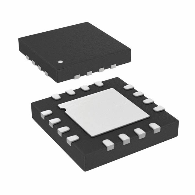
• Available in a tiny 10-pin EPAD-MSOP and 16-pin
QFN package
Applications
•
•
•
•
•
PON
Gigabit Ethernet
1X and 2X Fibre Channel
SONET/SDH: OC 3/12/24/48 – STM 1/4/8/16
High-gain line driver and line receiver
Markets
•
•
•
•
•
FTTX
Optical transceivers
Datacom/Telecom
Low-gain TIA interface
Long-reach FOM
Micrel Inc. • 2180 Fortune Drive • San Jose, CA 95131 • USA • tel +1 (408) 944-0800 • fax + 1 (408) 474-1000 • http:www.micrel.com
November 2007
M9999-110207-A
hbwhelp@micrel.com or (408) 955-1690
�Micrel, Inc.
SY88303BL
Typical Application
Pin Configuration
16-Pin QFN
10-Pin EPAD-MSOP (K10-2)
Ordering Information
Part Number
SY88303BLEY
(1)
SY88303BLEYTR
SY88303BLMG
(1)
SY88303BLMGTR
Package
Type
Operating
Range
Package Marking
Lead
Finish
K10-2
Industrial
303B with Pb-Free bar line indicator
Matte-Sn
Pb-free
K10-2
Industrial
303B with Pb-Free bar line indicator
Matte-Sn
Pb-free
QFN-16
Industrial
303B with Pb-Free bar line indicator
NiPdAu
Pb-free
QFN-16
Industrial
303B with Pb-Free bar line indicator
NiPdAu
Pb-free
Note:
1. Tape and Reel.
November 2007
2
M9999-110207-A
hbwhelp@micrel.com or (408) 955-1690
�Micrel, Inc.
SY88303BL
Pin Description
Pin Number
(MSOP)
Pin Number
(QFN)
Pin Name
Type
1
15
/EN
TTL Input:
Default is low.
2
1
DIN
Data Input
True data input with 50Ω termination to VREF.
3
4
/DIN
Data Input
Complementary data input w50Ω termination to VREF.
4
6
VREF
5
14
LOSLVL
Input
6
Exposed Pad
2, 3, 10, 11
Exposed Pad
GND
Ground
Pin Function
Enable bar: De-asserts true data output when High.
Reference Voltage: Placing a capacitor here to VCC
helps stabilize.
Loss-of-Signal Level Set: A resistor from this pin to VCC
sets the threshold for the data input amplitude at which
the LOS output will be asserted.
Device ground. Exposed pad must be connected to
PCB ground plane.
Loss-of-Signal: Asserts high when the data input
amplitude falls below the threshold sets by LOSLVL.
7
7
LOS
Open Collector
TTL Output
8
9
/DOUT
CML Output
Complementary data output.
9
12
DOUT
CML Output
True data output.
10
5, 8, 13, 16
VCC
Power Supply
November 2007
3
For proper operation, install an external 4.75k Ω pull-up
resistor at this output.
Positive power supply.
M9999-110207-A
hbwhelp@micrel.com or (408) 955-1690
�Micrel, Inc.
SY88303BL
Absolute Maximum Ratings(1)
Operating Ratings(2)
Supply Voltage (VCC) .................................... 0V to +4.0V
Input Voltage (DIN, DIN) .................................... 0 to VCC
Output Current (IOUT)
Continuous .....................................................+50mA
Surge ...........................................................+100mA
/EN Voltage ........................................................ 0 to VCC
VREF Current ....................................... -800µA to +500µA
LOSLVL Voltage .............................................. VREF to VCC
Lead Temperature (soldering, 20sec.) .................. 260°C
Storage Temperature (Ts) .....................-65°C to +150°C
Supply Voltage (VCC)............................ +3.0V to +3.6V
Ambient Temperature (TA) .................. –40°C to +85°C
Junction Temperature (TJ) ................ –40°C to +125°C
(3)
Junction Thermal Resistance
EPAD-MSOP
o
θJA (Still-Air) ............................................... 38 CW
o
ψJB ............................................................. 22 CW
QFN
o
θJA (Still-Air) ............................................... 61 CW
o
ψJB ............................................................. 38 CW
DC Electrical Characteristics
o
VCC = 3.0V to 3.6V; RL = 50Ω to VCC; TA = –40°C to +85°C; typical values at VCC = 3.3V, TA = 25 C.
Symbol
Parameter
Condition
ICC
Power Supply Current
No output load
Min
Typ
Max
Units
38
60
mA
VCC
V
VCC
V
VCC-0.350
V
+80
mV
VLOSLVL
LOSLVL Voltage
VOH
CML Output HIGH Voltage
VCC-0.020 VCC-0.005
VREF
VOL
CML Output LOW Voltage
VCC-0.475
VOFFSET
Differential Output Offset
VREF
Reference Voltage
ZI
Single-Ended Input Impedance
VCC-0.4
VCC-1.48
VCC-1.32
VCC-1.16
V
40
50
60
Ω
Min
Typ
Max
Units
TTL DC Electrical Characteristics
VCC = 3.0V to 3.6V; TA = –40°C to +85°C.
Symbol
Parameter
Condition
VIH
/EN Input HIGH Voltage
VIL
/EN Input LOW Voltage
2.0
IIH
/EN Input HIGH Current
VIN = 2.7V
IIL
/EN Input LOW Current
VIN = 0.5V
IOH
LOS Output Leakage
VOH = 3.6V
100
µA
VOL
LOS Output LOW Level
IOL = +4mA
0.5
V
VIN = VCC
V
0.8
V
20
µA
100
-300
µA
µA
Notes:
1. Permanent device damage may occur if absolute maximum ratings are exceeded. This is a stress rating only and functional operation is not
implied at conditions other than those detailed in the operational sections of this data sheet. Exposure to absolute maximum rating conditions
for extended periods may affect device reliability.
2. The data sheet limits are not guaranteed if the device is operated beyond the operating ratings.
3. Thermal performance assumes the use of a 4-layer PCB. Exposed pad must be soldered (or equivalent) to the device’s most negative
potential on the PCB.
November 2007
4
M9999-110207-A
hbwhelp@micrel.com or (408) 955-1690
�Micrel, Inc.
SY88303BL
AC Electrical Characteristics
VCC = 3.0V to 3.6V; RL = 50Ω to VCC; TA = –40°C to +85°C; typical values at VCC = 3.3V, TA = +25°C.
Symbol
Parameter
Condition
tr , tf
Output Rise/Fall Time
(20% to 80%)
tJITTER
Min
Typ
Max
Note 4
60
120
Deterministic
Random
Note 5
Note 6
15
5
VID
Differential Input Voltage Swing
Figure 1
10
VOD
Differential Output Voltage Swing
VID > 12mVPP, Figure 1
700
TOFF
LOS De-assert Time
TON
LOS Assert Time
LOSDL
Low LOS De-assert Level
R = 15kΩ, Note 8
27
mVPP
LOSAL
Low LOS Assert Level
R = 15kΩ, Note 8
18
mVPP
HYSL
Low LOS Hysteresis
R = 15kΩ, Note 7
3.4
dB
LOSDM
Medium LOS De-assert Level
R = 5kΩ, Note 8
LOSAM
Medium LOS Assert Level
R = 5kΩ, Note 8
21
36
HYSM
LOS Hysteresis
R = 5kΩ, Note 7
2
3.5
LOSDH
High LOS De-assert Level
R = 100Ω, Note 8
LOSAH
High LOS Assert Level
R = 100Ω, Note 8
70
94
HYSH
High LOS Hysteresis
R = 100Ω, Note 7
2
B-3dB
3dB Bandwidth
3.5
2
AV(Diff)
Differential Voltage Gain
S21
Single-ended Small-Signal Gain
ps
psPP
psRMS
1800
mVPP
800
950
mVPP
2
10
µs
2
10
53
137
26
Units
80
µs
mVPP
mVPP
6
200
dB
mVPP
mVPP
6
dB
GHz
39
dB
33
dB
Notes:
4.
5.
6.
7.
Amplifier in limiting mode. Input is a 200MHz, 100mVPP square wave.
Deterministic jitter measured using 3.2Gbps K28.5 pattern, VID = 10mVPP.
Random jitter measured using 3.2Gbps K28.7 pattern, VID = 10mVPP.
This specification defines electrical hysteresis as 20log (LOS De-assert/LOS Assert). The ratio between optical hysteresis and electrical
hysteresis is found to vary between 1.5 and 2, depending upon the level of received optical power and ROSA characteristics. Based upon that
ratio, the optical hysteresis corresponding to the electrical hysteresis range 2dB-6dB, shown in the AC characteristics table, will be 1dB-3dB
Optical Hysteresis.
8. See “Typical Operating Characteristics” for a graph showing how to choose a particular RLOSLVL for a particular LOS assert and its associated
de-assert amplitude.
November 2007
5
M9999-110207-A
hbwhelp@micrel.com or (408) 955-1690
�Micrel, Inc.
SY88303BL
Typical Operating Characteristics
Functional Characteristics
November 2007
6
M9999-110207-A
hbwhelp@micrel.com or (408) 955-1690
�Micrel, Inc.
SY88303BL
Functional Block Diagram
The SY88303BL low-power limiting post amplifiers
operate from a single +3.3V power supply, over
o
o
temperatures from –40 C to +85 C. Signals with data
rates up to 3.2Gbps and as small as 10mVPP can be
amplified. Figure 1 shows the allowed input voltage
swing. The SY88303BL generates a LOS output
allowing feedback to /EN for output stability. LOSLVL sets
the sensitivity of the input amplitude detection.
Input Amplifier Buffer
Figure 2 shows a simplified schematic of the input
stage. The high-sensitivity of the input amplifier allows
signals as small as 10mVPP to be amplified. The input
amplifier also allows input signals as large as
1800mVPP. Input signals below 12mVpp are linearly
amplified with a typical 42dB differential voltage gain.
Since it is a limiting amplifier, these devices output
typically 800mVPP voltage-limited waveforms for input
signals greater than 12mVPP. Applications requiring the
SY88303BL to operate with strong signals should have
the upstream TIA placed as close as possible to the
devices’ input pins. This ensures the best performance
of the device.
Output Buffer
The SY88303BL CML output buffers are designed to
drive 50Ω lines. The output buffer requires appropriate
termination for proper operation. An external
Ω 50
resistor to VCC for each output pin provides this. Figure 3
shows a simplified schematic of the output stage.
Loss-of-Signal
The SY88303BL generates a chatter-free LOS opencollector TTL output, as shown in Figure 4. LOS is used
to determine that the input amplitude is large enough to
be considered a valid input. LOS asserts high if the input
amplitude falls below the threshold sets by LOSLVL and
de-asserts low otherwise. LOS can be fed back to the
enable bar (/EN) input to maintain output stability under
a loss-of-signal condition. /EN de-asserts the true output
signal without removing the input signals.
Loss-of-Signal Level Set
Programmable LOS level-set pin (LOSLVL) sets the
threshold of the input amplitude detection. Connecting
an external resistor between VCC and LOSLVL set the
voltage at LOSLVL. This voltage ranges from VCC to VREF.
The external resistor creates a voltage divider between
VCC and VREF, as shown in Figure 5.
Hysteresis
The SY88303BL typically provides 3.5dB LOS electrical
hysteresis. By definition, a power ratio measured in dB
2
is 10log (power ratio). Power is calculated as V IN / R for
an electrical signal. Hence, the same ratio can be stated
as 20log (voltage ratio). While in linear mode, the
electrical voltage input changes linearly with the optical
power and therefore, the ratios change linearly. Thus,
the optical hysteresis in dB is half the electrical
hysteresis in dB given in the data sheet. Since the
SY88303BL is an electrical device, this data sheet refers
to hysteresis in electrical terms. With 3.5dB LOS
hysteresis, a voltage factor of 1.5 is required to assert or
de-assert LOS.
November 2007
7
Detailed Description
M9999-110207-A
hbwhelp@micrel.com or (408) 955-1690
�Micrel, Inc.
SY88303BL
Figure 1. VIS and VID
Figure 2. Input Structure
Figure 3. Output Structure
Figure 4. LOS Output Structure
Figure 5. LOSLVL Setting Circuit
November 2007
8
M9999-110207-A
hbwhelp@micrel.com or (408) 955-1690
�Micrel, Inc.
SY88303BL
Package Information
10-Pin EPAD-MSOP (K10-2)
November 2007
9
M9999-110207-A
hbwhelp@micrel.com or (408) 955-1690
�Micrel, Inc.
SY88303BL
16-Pin QFN
PCB Thermal Consideration for 16-Pin QFN® Package
(Always solder, or equivalent, the exposed pad to the PCB)
Package Notes:
1.
November 2007
Package meets Level 2 qualification.
2.
All parts are dry-packaged before shipment.
3.
Exposed pad must be soldered to a ground for proper thermal management,
solder void has to be less than 50% of the epad area.
10
M9999-110207-A
hbwhelp@micrel.com or (408) 955-1690
�Micrel, Inc.
SY88303BL
MICREL, INC. 2180 FORTUNE DRIVE SAN JOSE, CA 95131 USA
TEL +1 (408) 944-0800 FAX +1 (408) 474-1000 WEB http:www.micrel.com
The information furnished by Micrel in this data sheet is believed to be accurate and reliable. However, no responsibility is assumed by Micrel for
its use. Micrel reserves the right to change circuitry and specifications at any time without notification to the customer.
Micrel Products are not designed or authorized for use as components in life support appliances, devices or systems where malfunction of a
product can reasonably be expected to result in personal injury. Life support devices or systems are devices or systems that (a) are intended for
surgical implant into the body or (b) support or sustain life, and whose failure to perform can be reasonably expected to result in a significant injury
to the user. A Purchaser’s use or sale of Micrel Products for use in life support appliances, devices or systems is a Purchaser’s own risk and
Purchaser agrees to fully indemnify Micrel for any damages resulting from such use or sale.
© 2007 Micrel, Incorporated.
November 2007
11
M9999-110207-A
hbwhelp@micrel.com or (408) 955-1690
�


 工商网监
湘ICP备2023018690号
工商网监
湘ICP备2023018690号
