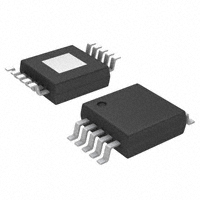
SY88313BL
3.3V, 3.2Gbps CML Low-Power Limiting Post
Amplifier with TTL Loss-of-Signal
General Description
The SY88313BL low-power limiting post amplifier is
designed for use in fiber-optic receivers. The device
connects to typical transimpedance amplifiers (TIAs).
The linear signal output from TIAs can contain
significant amounts of noise and may vary in amplitude
over time. The SY88313BL quantizes these signals and
outputs CML-level waveforms.
The SY88313BL operates from a single +3.3V ±10%
supply, over temperatures ranging from –40°C to +85°C.
With its wide bandwidth and high gain, signals with data
rates up to 3.2Gbps, and as small as 10mVPP, can be
amplified to drive devices with CML inputs or ACcoupled CML/PECL inputs.
The SY88313BL generates a loss-of-signal (LOS) opencollector TTL output. A programmable loss-of-signal
level set pin (LOSLVL) sets the sensitivity of the input
amplitude detection. LOS asserts high if the input
amplitude falls below the threshold set by LOSLVL and
de-asserts low otherwise. The enable bar input (/EN)
de-asserts the true output signal without removing the
input signal. The LOS output can be fed back to the /EN
input to maintain output stability under a loss-of-signal
condition. Typically, 3.4dB LOS hysteresis is provided to
prevent chattering.
Datasheet and support documentation cab be found on
Micrel’s web site at: www.micrel.com.
Features
•
Single 3.3V power supply
•
DC to 3.2Gbps operation
•
Low-noise CML data outputs
•
Chatter-free Open-Collector TTL loss-of-signal
(LOS) output with internal 4.75kΩ pull-up
resistor
•
TTL /EN input
•
Internal 50Ω input termination
•
Programmable LOS level set (LOSLVL)
•
Ideal for multi-rate applications
•
Available in a tiny 10-pin EPAD MSOP and
16-pin QFN package
Applications
•
APON/BPON, GEPON, EPON, and GPON
•
Gigabit Ethernet
•
Fibre Channel
•
OC-3/12/24/48 SONET/SDH
•
High-gain line driver and line receiver
•
Low-gain TIA interface
Markets
•
FTTP/FTTH
•
Datacom/Telecom
• Optical Transceivers
_______________________________________________________________________________________________________
Typical Application
Micrel Inc. • 2180 Fortune Drive • San Jose, CA 95131 • USA • tel +1 (408) 944-0800 • fax + 1 (408) 474-1000 • http://www.micrel.com
February 2007
M9999-021207-B
hbwhelp@micrel.com or (408) 955-1690
�Micrel, Inc.
SY88313BL
Ordering Information(1)
Part Number
Package
Type
Operating
Range
Package
Marking
Lead
Finish
SY88313BLMG
QFN-16
Industrial
313B with
Pb-Free bar-line indicator
NiPdAu
Pb-Free
QFN-16
Industrial
313B with
Pb-Free bar-line indicator
NiPdAu
Pb-Free
K10-2
Industrial
313B with
Pb-Free bar-line indicator
Matte-Sn
Pb-Free
K10-2
Industrial
313B with
Pb-Free bar-line indicator
Matte-Sn
Pb-Free
(2)
SY88313BLMGTR
SY88313BLEY
(2)
SY88313BLEYTR
Notes:
1. Contact factory for die availability. Dice are guaranteed at TA = 25C, DC Electricals only.
2. Tape and Reel.
Pin Configuration
16-Pin QFN
February 2007
10-Pin EPAD-MSOP (K10-2)
2
M9999-021207-B
hbwhelp@micrel.com or (408) 955-1690
�Micrel, Inc.
SY88313BL
Pin Description
Pin Number
(MSOP)
Pin Number
(QFN)
Pin Name
Type
1
15
/EN
TTL Input: Default is
high.
2
1
DIN
Data Input
True data input with 50Ω termination to VREF.
3
4
/DIN
Data Input
Complementary data input with 50Ω termination to
VREF.
4
6
VREF
5
14
LOSLVL
Input: Default is
maximum sensitivity
6
Exposed Pad
2, 3, 10, 11
Exposed
Pad
GND
Ground
7
7
LOS
Open Collector TTL
Output with Internal
4.75kΩ pull-up
resistor
8
9
/DOUT
CML Output
Complementary data output.
9
12
DOUT
CML Output
True data output.
10
5, 8, 13, 16
VCC
Power Supply
February 2007
Pin Function
Enable Bar: De-assert true data output when high.
Reference Voltage: Placing a capacitor here to VCC
helps stabilize LOSLVL.
Loss-of-Signal Level Set: A resistor from this pin to VCC
sets the threshold for the data input amplitude at which
the LOS output will be asserted.
Device ground. Exposed pad must be connected to
PCB ground plane.
Loss-of-Signal: Asserts high when the data input
amplitude falls below the threshold set by LOSLVL.
Positive power supply.
3
M9999-021207-B
hbwhelp@micrel.com or (408) 955-1690
�Micrel, Inc.
SY88313BL
Operating Ratings(2)
Absolute Maximum Ratings(1)
Supply Voltage (VCC) ........................... +3.0V to +3.6V
Ambient Temperature (TA).................. –40°C to +85°C
Junction Temperature (TJ) ................ –40°C to +120°C
(3)
Junction Thermal Resistance
QFN
(θJA) Still-air .................................................. 61°C/W
(ψJB) .............................................................. 38°C/W
Supply Voltage (VCC) ..................................... +0V to +4.0V
Input Voltage (DIN, /DIN) .......................................0 to VCC
Output Current (IOUT) .............................................. ± 25mA
/EN Voltage ............................................................0 to VCC
VREF Current ............................................................ ±1mA
LOSLVL Voltage............................................... VREF to VCC
Lead Temperature (soldering, 20sec.) ................... +260°C
Storage Temperature (Ts) ........................ -65°C to +150°C
EPAD-MSOP
(θ JA) Still-air .................................................. 38°C/W
(ψJB) .............................................................. 22°C/W
DC Electrical Characteristics
VCC = 3.0V to 3.6V; RL = 50Ω to VCC; TA = –40°C to +85°C, unless otherwise stated.
Symbol
Parameter
Condition
Min
ICC
Power Supply Current
No output load.
LOSLVL
LOSLVL Voltage
VOH
CML Output HIGH Voltage
VOL
CML Output LOW Voltage
VOFFSET
Differential Output Offset
ZO
Single-Ended Output Impedance
40
ZI
Single-Ended Input Impedance
40
VREF
Reference Voltage
Typ
47
VREF
VCC = 3.3V
Max
Units
65
mA
VCC
V
V
VCC-0.020
VCC-0.005
VCC
VCC-0.475
VCC-0.400
VCC-0.350
V
±80
mV
50
60
Ω
50
60
Ω
VCC-1.28
V
TTL DC Electrical Characteristics
VCC = 3.0V to 3.6V; RL = 50Ω to VCC; TA = –40°C to +85°C, unless otherwise stated.
Symbol
Parameter
Condition
Min
Typ
Max
Units
0.8
V
20
100
µA
µA
VIH
/EN Input HIGH Voltage
VIL
/EN Input LOW Voltage
2.0
V
IIH
/EN Input HIGH Current
VIN = 2.7V
VIN = VCC
IIL
/EN Input LOW Current
VIN = 0.5V
-0.3
mA
VOH
LOS Output HIGH Level
VCC ≥ 3.3V, IOH (max)
很抱歉,暂时无法提供与“SY88313BLEY”相匹配的价格&库存,您可以联系我们找货
免费人工找货