2.5V, 3.2Gbps DUAL, DIFFERENTIAL
2:1 LVDS MULTIPLEXER WITH
INTERNAL TERMINATION
Micrel, Inc.
Precision Edge®
SY89542U
®
Precision Edge
SY89542U
FEATURES
■ Dual 2:1 multiplexer
■ Guaranteed AC performance over temp and voltage:
• DC-to > 3.2Gbps data rate throughput
• < 600ps In-to-Out tpd
• < 150ps tr/tf
■ Ultra-low jitter design:
• < 1psRMS random jitter
• < 10psPP deterministic jitter
• < 10psPP total jitter (clock)
• < 0.7psRMS crosstalk-induced jitter
■ Unique input isolation design minimizes crosstalk
■ Internal input termination
■ Unique input termination and VT pin accepts
DC-Coupled and AC-coupled inputs (LVDS, LVPECL,
CML)
■ 350mV LVDS output swing
■ CMOS/TTL compatible MUX select
■ Power supply 2.5V ±5%
■ –40°C to +85°C temperature range
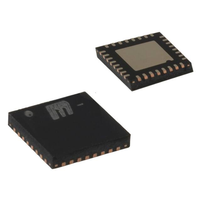
■ Available in 32-pin (5mm x 5mm) MLF® package
Precision Edge®
DESCRIPTION
The SY89542U includes two precision, high-speed 2:1
differential Muxes with LVDS (350mV) compatible outputs
with a guaranteed data rate throughput of 3.2Gbps over
temperature and voltage.
The SY89542U differential inputs include a unique, 3-pin
internal termination that allows access to the termination
network through a VT pin. This feature allows the device to
easily interface to different logic standards, both AC- and
DC-coupled without external resistor-bias and termination
networks. The result is a clean, stub-free, low jitter interface
solution.
The SY89542U operates from a single 2.5V supply, and
is guaranteed over the full industrial temperature range
(–40°C to +85°C). For applications that require a 3.3V supply,
consider the SY89543L. The SY89542U is part of Micrel’s
Precision Edge® product family.
All support documentation can be found on Micrel’s web
site at www.micrel.com.
APPLICATIONS
■
■
■
■
Redundant clock/data switchover
SONET/SDH multi-channel select applications
Fibre Channel applications
GigE applications
FUNCTIONAL BLOCK DIAGRAM
INA0
INB0
50Ω
50Ω
VTB0
50Ω
VTA0
50Ω
2:1 MUX
/INA0
0
2:1 MUX
/INB0
0
LVDS
MUX A
QA
LVDS
MUX B
/QA
1
/QB
1
S
INA1
QB
S
INB1
50Ω
50Ω
VTB1
50Ω
VTA1
50Ω
/INA1
/INB1
SELA (CMOS/TTL)
SELB (CMOS/TTL)
Precision Edge is a registered trademark of Micrel, Inc.
MicroLeadFrame and MLF are registered trademarks of Amkor Technology, Inc.
M9999-082407
hbwhelp@micrel.com or (408) 955-1690
Rev.: D
1
Amendment: /0
Issue Date: August 2007
�Precision Edge®
SY89542U
Micrel, Inc.
PACKAGE/ORDERING INFORMATION
INA1
VTA1
/INA1
VCC
VCC
INB0
VTB0
/INB0
Ordering Information(1)
32 31 30 29 28 27 26 25
1
24
2
23
3
22
4
21
5
20
6
19
7
18
8
9 10 11 12 13 14 15 16
17
VCC
INB1
VTB 1
/INB1
VCC
SELB
GND
VCC
GND
QA
/QA
GND
GND
QB
/QB
GND
VCC
/INA0
VTA0
INA0
VCC
SELA
GND
VCC
32-Pin MLF®
Part Number
Package
Type
Operating
Range
Package
Marking
Lead
Finish
SY89542UMI
MLF-32
Industrial
SY89542U
Sn-Pb
SY89542UMITR(2)
MLF-32
Industrial
SY89542U
Sn-Pb
SY89542UMG(3)
MLF-32
Industrial
SY89542U with
Pb-Free bar-line indicator
Pb-Free
NiPdAu
SY89542UMGTR(2,3)
MLF-32
Industrial
SY89542U with
Pb-Free bar-line indicator
Pb-Free
NiPdAu
Notes:
1. Contact factory for die availability. Dice are guaranteed at TA = 25°C, DC electricals only.
2. Tape and Reel.
3. Recommended for new designs.
PIN DESCRIPTION
Pin Number
Pin Name
4, 2, 32, 30,
27, 25, 23, 21
INA0, /INA0,
INA1, /INA1,
INB0, /INB0,
INB1, /INB1
Differential Inputs: These input pairs are the differential signal inputs to the device. Inputs
accept AC- or DC-coupled signals as small as 100mV. Each pin of a pair internally
terminates to a VT pin through 50Ω. Note that these inputs will default to an indeterminate
state if left open. Unused differential input pairs can be terminated by connecting one input
to VCC and the complementary input to GND through a 1kΩ resistor. The VT pin is to be
left open in this configuration. Please refer to the “Input Interface Applications” section for
more details.
3, 31, 26, 22
VTA0 , VTA1,
VTB0, VTB1
Input Termination Center-Tap: Each side of the differential input pair, terminates to a VT
pin. The VTA0, VTA1, VTB0, VTB1 pins provide a center-tap to a termination network for
maximum interface flexibility. See “Input Interface Applications” section for more details.
6, 19
SELA, SELB
These single-ended TTL/CMOS-compatible inputs select the inputs to the multiplexers.
Note that these inputs are internally connected to a 25kΩ pull-up resistor and will default
to logic HIGH state if left open. Input switching threshold is VCC/2.
1, 5, 8, 17, 20,
24, 28, 29
VCC
10, 11, 14, 15
QA, /QA,
QB, /QB
7, 9, 12, 13, 16, 18
GND,
Exposed pad
M9999-082407
hbwhelp@micrel.com or (408) 955-1690
Pin Function
Positive Power Supply: Bypass with 0.1µF||0.01µF low ESR capacitors. The 0.01µF
capacitor should be as close to VCC pin as possible.
Differential Outputs: This differential LVDS output pair provides a copy of the selected
input. It is a logic function of the INA0, INA1, INB0, INB1 and SELA and SELB inputs.
Please refer to the “Truth Table” for details. Unused output pairs must be terminated with
100Ω across the differential pair.
Ground: Ground pin and exposed pad must be connected to the same ground plane.
2
�Precision Edge®
SY89542U
Micrel, Inc.
Absolute Maximum Ratings(1)
Operating Ratings(2)
Supply Voltage (VCC) ................................. –0.5V to +4.0V
Input Voltage (VIN) ........................................ –0.5V to VCC
Termination Current(3)
Source or sink current on VT ..................................... ±100mA
Input Current
Source or sink current on IN, /IN .......................... ±50mA
Lead Temperature (soldering, 20 sec.) ................... +260°C
Storage Temperature (TS) ....................... –65°C to +150°C
Supply Voltage (VCC) ............................. 2.375V to 2.625V
Ambient Temperature (TA) ........................ –40°C to +85°C
Package Thermal Resistance(4)
MLF® (θJA)
Still-Air ................................................................ 35°C/W
500lfpm .............................................................. 28°C/W
MLF® (ψJB)
Junction-to-Board ................................................ 20°C/W
DC ELECTRICAL CHARACTERISTICS(5)
TA = –40°C to +85°C; Unless otherwise stated.
Symbol
Parameter
VCC
Power Supply
Condition
No Load, Max. VCC
Min
Typ
Max
Units
2.375
2.5
2.625
V
70
95
mA
(6)
ICC
Power Supply Current
RDIFF_IN
Differential Input Resistance
(IN-to-/IN)
80
100
120
Ω
RIN
Input Resistance
(IN-to-VT, /IN-to-VT)
40
50
60
Ω
VIH
Input High Voltage (IN, /IN)
1.2
VCC
V
VIL
Input Low Voltage (IN, /IN)
0
VIH–0.1
V
VIN
Input Voltage Swing (IN, /IN)
Notes 7
0.1
VCC
V
VDIFF_IN
Differential Input Voltage Swing
|IN - /IN|
Notes 7
0.2
IN-to-VT
Voltage from Input to VT
V
1.8
V
Notes:
1. Permanent device damage may occur if “Absolute Maximum Ratings” are exceeded. This is a stress rating only and functional operation is not
implied at conditions other than those detailed in the operational sections of this data sheet. Exposure to “Absolute Maximum Ratings” conditions for
extended periods may affect device reliability.
2. The data sheet limits are not guaranteed if the device is operated beyond the operating ratings.
3. Due to the limited drive capability use for input of the same package only.
4. Package thermal resistance assumes exposed pad is soldered (or equivalent) to the device’s most negative potential on the PCB. ΨJB uses 4-layer
θJA in still-air unless otherwise stated.
5. The circuit is designed to meet the DC specifications shown in the above table after thermal equilibrium has been established.
6. Includes current through internal 50Ω pull-ups.
7. See “Single-Ended and Differential Swings” section for VIN and VDIFF_IN definition.
M9999-082407
hbwhelp@micrel.com or (408) 955-1690
3
�Precision Edge®
SY89542U
Micrel, Inc.
LVDS OUTPUTS DC ELECTRICAL CHARACTERISTICS(9)
VCC = 2.5V ±5%; TA = –40°C to +85°C; RL = 100Ω across Q and /Q, unless otherwise stated.
Symbol
Parameter
Condition
Min
Typ
Max
Units
VOH
Output HIGH Voltage (Q, /Q)
See Figure 5a
1.475
V
VOL
Output LOW Voltage (Q, /Q)
See Figure 5a
VOUT
Output Voltage Swing (Q, /Q)
See Figures 1a, 5a
250
350
mV
VDIFF-OUT
Differential Output Voltage Swing
|Q - /Q|
See Figure 1b
500
700
mV
VOCM
Output Common Mode Voltage
(Q, /Q)
See Figure 5b
1.125
1.275
V
∆VOCM
Change in Common Mode Voltage
(Q, /Q)
See Figure 5b
–50
+50
mV
Max
Units
VCC
V
0.925
V
LVTTL/CMOS DC ELECTRICAL CHARACTERISTICS(9)
VCC = 2.5V ±5%; TA = –40°C to +85°C; unless otherwise stated.
Symbol
Parameter
Condition
Min
Typ
VIH
Input HIGH Voltage
VIL
Input LOW Voltage
0.8
V
IIH
Input HIGH Current
40
µA
IIL
Input LOW Current
–300
µA
2.0
Note:
9. The circuit is designed to meet the DC specifications shown in the above table after thermal equilibrium has been established.
M9999-082407
hbwhelp@micrel.com or (408) 955-1690
4
�Precision Edge®
SY89542U
Micrel, Inc.
AC ELECTRICAL CHARACTERISTICS(10)
VCC = 2.5V ±5%; TA = –40°C to +85°C; RL = 100Ω across Q and /Q, unless otherwise stated.
Symbol
Parameter
Condition
fMAX
Maximum Operating Frequency
Min
NRZ Data
VOUT > 200mV
tpd
tSKEW
tJITTER
Differential Propagation Delay
Max
3.2
Clock
Units
Gbps
4
GHz
IN-to-Q
250
350
450
ps
SEL-to-Q
200
350
600
ps
Input-to-Input Skew
Note 11
20
ps
Bank-to-Bank Skew
Note 12
25
ps
Part-to-Part Skew
Note 13
200
ps
Data
Random Jitter (RJ)
Note 14
1
psRMS
Deterministic Jitter (DJ)
Note 15
10
psPP
Total Jitter (TJ )
Note 16
10
psPP
Cycle-to-Cycle Jitter
Note 17
1
psRMS
Crosstalk-Induced Jitter
Note 18
0.7
psRMS
150
ps
Clock
tr, tf
Typ
Output Rise / Fall Time
(20% to 80%)
At full output swing
35
80
Notes:
10. Measured with 100mV input swing. See “Timing Diagrams ” section for definition of parameters. High frequency AC-parameters are guaranteed by
design and characterization.
11. Input-to-input skew is the difference in time from an input-to-output in comparison to any other input-to-output. In addition, the input-to-input skew
does not include the output skew.
12. Bank-to-bank skew is the difference in time from input to the output between banks.
13. Part-to-part skew is defined for two parts with identical power supply voltages at the same temperature and with no skew of the edges at the
respective inputs. Total skew is calculated as the RMS (Root Mean Square) of the input skew and output skew.
14. Random jitter is measured with a K28.7 comma detect character pattern, measured at 1.25Gbps and 3.2Gbps.
15. Deterministic jitter is measured at 1.25Gbps and 3.2Gbps, with both K28.5 and 223–1 PRBS pattern.
16. Total jitter definition: with an ideal clock input of frequency ≤ fMAX, no more than one output edge in 1012 output edges will deviate by more than the
specified peak-to-peak jitter value.
17. Cycle-to-cycle jitter definition: the variation of periods between adjacent cycles, Tn-Tn-1 where T is the time between rising edges of the output signal.
18. Crosstalk is measured at the output while applying two similar frequencies to adjacent inputs that are asynchronous with respect to each other at the
inputs.
M9999-082407
hbwhelp@micrel.com or (408) 955-1690
5
�Precision Edge®
SY89542U
Micrel, Inc.
SINGLE-ENDED AND DIFFERENTIAL SWINGS
VDIFF_IN,
VDIFF_OUT 700mV (Typ.)
VIN,
VOUT 350mV (Typ.)
Figure 1a. Single-Ended Voltage Swing
Figure 1b. Differential Voltage Swing
TIMING DIAGRAM
IN
/IN
tpd
Q
/Q
SEL
SEL-to-Q
tpd
Q
/Q
Figure 2. Timing Diagram
TRUTH TABLE
IN0
IN1
SEL
Q
/Q
0
X
0
0
1
1
X
0
1
0
X
0
1
0
1
X
1
1
1
0
M9999-082407
hbwhelp@micrel.com or (408) 955-1690
6
�Precision Edge®
SY89542U
Micrel, Inc.
FUNCTIONAL CHARACTERISTICS
VCC = 2.5V, TA = 25°C.
200MHz Output
1.6GHz Output
Q
Output Swing
(70mV/div.)
Output Swing
(70mV/div.)
Q
/Q
/Q
TIME (600ps/div.)
TIME (80ps/div.)
2.5GHz Output
3.2GHz Output
Output Swing
(70mV/div.)
Output Swing
(70mV/div.)
Q
Q
/Q
/Q
TIME (40ps/div.)
OC-12 Mask (223–1 PRBS)
2xGBE Mask (223–1 PRBS)
Output Swing
(70mV/div.)
Output Swing
(70mV/div.)
TIME (50ps/div.)
TIME (270ps/div.)
TIME (67ps/div.)
3.2Gbps Data Output (223-1 PRBS)
Output Swing
(70mV/div.)
OUTPUT AMPLITUDE (mV)
400
350
300
250
200
150
100
50
0
0
TIME (80ps/div.)
M9999-082407
hbwhelp@micrel.com or (408) 955-1690
7
Output Amplitude
vs. Frequency
1
2
3
4
5
FREQUENCY (GHz)
6
�Precision Edge®
SY89542U
Micrel, Inc.
INPUT AND OUTPUT STAGE INTERNAL TERMINATION
VCC
IN
50Ω
VT
GND
50Ω
/IN
Figure 3. Simplified Differential Input Stage
INPUT INTERFACE APPLICATIONS
VCC
VCC
VCC
IN
LVPECL
IN
/IN
CML
IN
VCC
/IN
CML
/IN
SY89542U
SY89542U
GND
VT
VCC –1.4V
GND
Rp
VT
VT
NC
For VCC = 2.5V, Rp = 19Ω
GND
Figure 4a. CML
Interface (DC-Coupled)
Figure 4b. CML
Interface (AC-Coupled)
VCC
VCC
IN
LVPECL
IN
/IN
Rp
SY89542U
Rp
GND
LVDS
/IN
VCC –1.4V
GND
VT
SY89542U
GND
VT
NC
GND
For VCC = 2.5V, Rp = 50Ω
Figure 4d. LVPECL
Interface (AC-Coupled)
M9999-082407
hbwhelp@micrel.com or (408) 955-1690
GND
SY89542U
0.01µF
Figure 4e. LVDS Interface
8
Figure 4c. LVPECL
Interface (DC-Coupled)
�Precision Edge®
SY89542U
Micrel, Inc.
OUTPUT INTERFACE APPLICATIONS
LVDS specifies a small swing of 350mV typical, on a
nominal 1.25V common mode above ground. The common
mode voltage has tight limits to permit large variations in
ground between an LVDS driver and receiver. Also, change
in common mode voltage, as a function of data input, is
kept to a minimum, to keep EMI low.
50Ω
50Ω
50Ω
VOCM,
∆VOCM
50Ω
GND
VOCM,
∆VOCM
GND
Figure 5a. LVDS Differential Measurement
Figure 5b. LVDS Common Mode Measurement
RELATED MICREL PRODUCTS AND SUPPORT DOCUMENTATION
Part Number
Function
Data Sheet Link
SY89543L
3.3V, 3.2Gbps Dual, Differential 2:1 LVDS
Multiplexer with Internal Input Termination
http://www.micrel.com/_pdf/HBW/sy89543l.pdf
SY89544U
2.5V, 3.2Gbps 4:1 LVDS Multiplexer with Internal
Input Termination
http://www.micrel.com/_pdf/HBW/sy89544u.pdf
SY89545L
3.3V, 3.2Gbps 4:1 LVDS Multiplexer with Internal
Input Termination
http://www.micrel.com/_pdf/HBW/sy89545l.pdf
SY89546U
2.5V 3.2Gbps, Differential 4:1 LVDS Multiplexer
with 1:2 Fanout and Internal Input Termination
http://www.micrel.com/_pdf/HBW/sy89546u.pdf
SY89547L
3.3V 3.2Gbps, Differential 4:1 LVDS Multiplexer
with 1:2 Fanout and Internal Input Termination
http://www.micrel.com/_pdf/HBW/sy89547l.pdf
MLF® Application Note
www.amkor.com/products/notes_papers/LF_AppNote_0902.pdf
New Products and Applications
www.micrel.com/product-info/products/solutions.shtml
HBW Solutions
M9999-082407
hbwhelp@micrel.com or (408) 955-1690
9
�Precision Edge®
SY89542U
Micrel, Inc.
32-PIN MicroLeadFrame® (MLF-32)
Package
EP- Exposed Pad
Die
CompSide Island
Heat Dissipation
Heat Dissipation
VEE
Heavy Copper Plane
VEE
Heavy Copper Plane
PCB Thermal Consideration for 32-Pin MLF® Package
(Always solder, or equivalent, the exposed pad to the PCB)
Package Notes:
1. Package meets Level 2 qualification.
2. All parts are dry-packaged before shipment.
3. Exposed pads must be soldered to a ground for proper thermal management.
MICREL, INC. 2180 FORTUNE DRIVE SAN JOSE, CA 95131 USA
TEL
+ 1 (408) 944-0800
FAX
+ 1 (408) 474-1000
WEB
http://www.micrel.com
The information furnished by Micrel in this data sheet is believed to be accurate and reliable. However, no responsibility is assumed by Micrel for its use.
Micrel reserves the right to change circuitry and specifications at any time without notification to the customer.
Micrel Products are not designed or authorized for use as components in life support appliances, devices or systems where malfunction of a product can
reasonably be expected to result in personal injury. Life support devices or systems are devices or systems that (a) are intended for surgical implant into
the body or (b) support or sustain life, and whose failure to perform can be reasonably expected to result in a significant injury to the user. A Purchaser’s
use or sale of Micrel Products for use in life support appliances, devices or systems is at Purchaser’s own risk and Purchaser agrees to fully indemnify
Micrel for any damages resulting from such use or sale.
© 2006 Micrel, Incorporated.
M9999-082407
hbwhelp@micrel.com or (408) 955-1690
10
�