TC1070/TC1071/TC1187
50 mA, 100 mA and 150 mA Adjustable CMOS LDOs with Shutdown
Features:
Description:
•
•
•
•
The TC1070, TC1071 and TC1187 devices are
adjustable LDOs designed to supersede a variety of
older (bipolar) voltage regulators. Total supply current
is typically 50 µA at full load (20 to 60 times lower than
in bipolar regulators).
•
•
•
•
50 µA Ground Current for Longer Battery Life
Adjustable Output Voltage
Very Low Dropout Voltage
Choice of 50 mA (TC1070), 100 mA (TC1071)
and 150 mA (TC1187) Output
Power-Saving Shutdown mode
Overcurrent and Overtemperature Protection
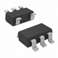
Space-Saving 5-Pin SOT-23 Package
Pin Compatible with Bipolar Regulators
Applications:
•
•
•
•
•
•
•
Battery Operated Systems
Portable Computers
Medical Instruments
Instrumentation
Cellular/GSM/PHS Phones
Linear Post-Regulators for SMPS
Pagers
The TC1070, TC1071 and TC1187 devices are stable
with an output capacitor of only 1 µF and have a
maximum output current of 50 mA, 100 mA and
150 mA, respectively. For higher output versions
please see the TC1174 (IOUT = 300 mA) data sheet
(DS21363).
Typical Application
VIN
1
VIN
Package Type
VOUT
SHDN
5
5-Pin SOT-23
VOUT
C1 +
1 µF
TC1070
TC1071
TC1187
2 GND
3
The devices’ key features include ultra low-noise
operation, very low dropout voltage – typically 85 mV
(TC1070), 180 mV (TC1071) and 270 mV (TC1187) at
full load and fast response to step changes in load.
Supply current is reduced to 0.5 µA (maximum) when
the shutdown input is low. The devices incorporate both
overtemperature and overcurrent protection. Output
voltage is programmed with a simple resistor divider
from VOUT to ADJ to GND.
VOUT
ADJ
5
4
R1
ADJ
TC1070
TC1071
TC1187
4
R2
1
VIN
Shutdown Control
(from Power Control Logic)
2
3
GND SHDN
R1
V OUT = V REF ------- + 1
R2
2010 Microchip Technology Inc.
DS21353E-page 1
�TC1070/TC1071/TC1187
1.0
ELECTRICAL
CHARACTERISTICS
† Notice: Stresses above those listed under "Absolute
Maximum Ratings" may cause permanent damage to
the device. These are stress ratings only and functional
operation of the device at these or any other conditions
above those indicated in the operation sections of the
specifications is not implied. Exposure to Absolute
Maximum Rating conditions for extended periods may
affect device reliability.
Absolute Maximum Ratings†
Input Voltage .........................................................6.5V
Output Voltage........................... (-0.3V) to (VIN + 0.3V)
Power Dissipation................Internally Limited (Note 5)
Maximum Voltage on Any Pin ........VIN +0.3V to -0.3V
Operating Temperature Range...... -40°C < TJ < 125°C
Storage Temperature..........................-65°C to +150°C
ELECTRICAL SPECIFICATIONS
Electrical Characteristics: VIN = VOUT + 1V, IL = 0.1 mA, CL = 3.3 µF, SHDN > VIH, TA = +25°C, unless otherwise
noted. Boldface type specifications apply for junction temperatures of -40°C to +125°C.
Parameter
Input Operating Voltage
Maximum Output Current
Adjustable Output
Voltage Range
Symbol
Min
Typ
Max
Units
Test Conditions
VIN
2.7
—
6.0
V
Note 6
IOUTmax
50
—
—
mA
TC1070
100
—
—
TC1071
150
—
—
TC1187
VOUT
VREF
—
5.5
V
VREF
1.165
1.20
1.235
V
VREF/T
—
40
—
ppm/°C
Line Regulation
VOUT/VIN
—
0.05
0.35
%
(VR + 1V) VIN6V
Load Regulation (Note 2)
VOUT/VOUT
—
0.5
2
%
TC1070, TC1071
IL = 0.1 mA to IOUTmax
—
0.5
3
Reference Voltage
VREF Temperature Coefficient
Note 1:
2:
3:
4:
5:
6:
Note 1
TC1187
IL = 0.1 mA to IOUTmax
TC VOUT = (VOUTmax – VOUTMIN) x 106
VOUTx T
Regulation is measured at a constant junction temperature using low duty cycle pulse testing. Load regulation is tested over a load range from 0.1 mA to the maximum specified output current. Changes in output
voltage due to heating effects are covered by the thermal regulation specification.
Dropout voltage is defined as the input to output differential at which the output voltage drops 2% below its
nominal value.
Thermal Regulation is defined as the change in output voltage at a time T after a change in power dissipation is applied, excluding load or line regulation effects. Specifications are for a current pulse equal to
Ilmax at VIN = 6V for T = 10 ms.
The maximum allowable power dissipation is a function of ambient temperature, the maximum allowable
junction temperature and the thermal resistance from junction-to-air (i.e., Ta, Tj, ja). Exceeding the maximum allowable power dissipation causes the device to initiate thermal shutdown. Please see Section 5.0
“Thermal Considerations” for more details.
The minimum VIN has to justify the conditions: VIN VR + VDROPOUT and VIN 2.7V for IL = 0.1 mA to
IOUTMAX.
DS21353E-page 2
2010 Microchip Technology Inc.
�TC1070/TC1071/TC1187
ELECTRICAL SPECIFICATIONS (CONTINUED)
Electrical Characteristics: VIN = VOUT + 1V, IL = 0.1 mA, CL = 3.3 µF, SHDN > VIH, TA = +25°C, unless otherwise
noted. Boldface type specifications apply for junction temperatures of -40°C to +125°C.
Parameter
Dropout Voltage (Note 3)
Supply Current
Shutdown Supply Current
Power Supply Rejection Ratio
Symbol
Min
Typ
Max
Units
VIN-VOUT
—
2
—
mV
IIN
Test Conditions
IL = 0.1 mA
—
65
—
IL = 20 mA
—
85
120
IL = 50 mA
—
180
250
TC1071, TC1187
IL = 100 mA
—
270
400
TC1187
IL = 150 mA
—
50
80
µA
SHDN = VIH, IL = 0
IINSD
—
0.05
0.5
µA
SHDN = 0V
PSRR
—
64
—
dB
FRE1 kHz
IOUTSC
—
300
450
mA
VOUT = 0V
Thermal Regulation
VOUT/PD
—
0.04
—
V/W
Note 4
Thermal Shutdown
Die Temperature
TSD
—
160
—
°C
TSD
—
10
—
°C
eN
—
260
—
nV/Hz
SHDN Input High Threshold
VIH
45
—
—
%VIN
VIN = 2.5V to 6.5V
SHDN Input Low Threshold
VIL
—
—
15
%VIN
VIN = 2.5V to 6.5V
IADJ
—
50
—
pA
Output Short Circuit Current
Thermal Shutdown Hysteresis
Output Noise
IL = IOUTmax
SHDN Input
ADJ Input
Adjust Input Leakage Current
Note 1:
2:
3:
4:
5:
6:
TC VOUT = (VOUTmax – VOUTMIN) x 106
VOUTx T
Regulation is measured at a constant junction temperature using low duty cycle pulse testing. Load regulation is tested over a load range from 0.1 mA to the maximum specified output current. Changes in output
voltage due to heating effects are covered by the thermal regulation specification.
Dropout voltage is defined as the input to output differential at which the output voltage drops 2% below its
nominal value.
Thermal Regulation is defined as the change in output voltage at a time T after a change in power dissipation is applied, excluding load or line regulation effects. Specifications are for a current pulse equal to
Ilmax at VIN = 6V for T = 10 ms.
The maximum allowable power dissipation is a function of ambient temperature, the maximum allowable
junction temperature and the thermal resistance from junction-to-air (i.e., Ta, Tj, ja). Exceeding the maximum allowable power dissipation causes the device to initiate thermal shutdown. Please see Section 5.0
“Thermal Considerations” for more details.
The minimum VIN has to justify the conditions: VIN VR + VDROPOUT and VIN 2.7V for IL = 0.1 mA to
IOUTMAX.
TERMPERATURE CHARACTERISTICS
Parameters
Thermal Resistance, 5L-SOT-23
2010 Microchip Technology Inc.
Sym
Min
Typ
Max
Units
JA
—
256
—
°C/W
Conditions
DS21353E-page 3
�TC1070/TC1071/TC1187
2.0
TYPICAL CHARACTERISTICS
Note:
The graphs and tables provided following this note are a statistical summary based on a limited number of
samples and are provided for informational purposes only. The performance characteristics listed herein
are not tested or guaranteed. In some graphs or tables, the data presented may be outside the specified
operating range (e.g., outside specified power supply range) and therefore outside the warranted range.
Note: Unless otherwise specified, all parts are measured at temperature = +25°C.
DROPOUT VOLTAGE (V)
0.018
Dropout Voltage vs. Temperature (VOUT = 3.3V)
ILOAD = 10mA
0.090
0.016
0.014
0.012
0.010
0.008
0.006
0.004
0.002
0.100
DROPOUT VOLTAGE (V)
0.020
CIN = 1μF
COUT = 1μF
-20
0
20
50
TEMPERATURE (°C)
70
0.030
0.020
0.300
CIN = 1μF
COUT = 1μF
0.012
0.010
0.008
0.006
0.004
CIN = 1μF
COUT = 1μF
-40
-20
0
20
50
TEMPERATURE (°C)
70
125
60
50
40
30
20
CIN = 1μF
COUT = 1μF
0
0 0.5 1 1.5 2 2.5 3 3.5 4 4.5 5 5.5 6 6.5 7 7.5
VIN (V)
0.250
0.200
0.150
0.100
0.050
90
CIN = 1μF
COUT = 1μF
-20
0
20
50
TEMPERATURE (°C)
70
125
Ground Current vs. VIN (VOUT = 3.3V)
ILOAD = 100mA
80
GND CURRENT (μA)
70
DS21353E-page 4
70
Dropout Voltage vs. Temperature (VOUT = 3.3V)
-40
ILOAD = 10mA
10
0
20
50
TEMPERATURE (°C)
0.000
125
Ground Current vs. VIN (VOUT = 3.3V)
80
-20
ILOAD = 150mA
0.000
GND CURRENT (μA)
0.040
ILOAD = 10mA
0.014
90
0.050
-40
Dropout Voltage vs. Temperature (VOUT = 3.3V)
0.016
0.002
0.060
125
DROPOUT VOLTAGE (V)
DROPOUT VOLTAGE (V)
0.018
0.070
0.000
-40
0.020
ILOAD = 50mA
0.080
0.010
0.000
Dropout Voltage vs. Temperature (VOUT = 3.3V)
70
60
50
40
30
20
CIN = 1μF
COUT = 1μF
10
0
0 0.5 1 1.5 2 2.5 3 3.5 4 4.5 5 5.5 6 6.5 7 7.5
VIN (V)
2010 Microchip Technology Inc.
�TC1070/TC1071/TC1187
Note: Unless otherwise specified, all parts are measured at temperature = +25°C.
Ground Current vs. VIN (VOUT = 3.3V)
80
ILOAD = 0
ILOAD = 150mA
3
60
2.5
50
VOUT (V)
GND CURRENT (μA)
70
40
30
2
1.5
1
20
0.5
CIN = 1μF
COUT = 1μF
10
0
CIN = 1μF
COUT = 1μF
0
0
0 0.5 1 1.5 2 2.5 3 3.5 4 4.5 5 5.5 6 6.5 7 7.5
VIN (V)
0.5 1 1.5
2 2.5 3 3.5
4 4.5 5
5.5 6 6.5 7
VIN (V)
VOUT vs. VIN (VOUT = 3.3V)
3.5
3.0
VOUT vs. VIN (VOUT = 3.3V)
3.5
Output Voltage vs. Temperature (VOUT = 3.3V)
3.320
ILOAD = 100mA
ILOAD = 10mA
3.315
3.310
3.305
VOUT (V)
VOUT (V)
2.5
2.0
1.5
3.300
3.295
3.290
1.0
3.285
0.5
CIN = 1μF
COUT = 1μF
0.0
0
3.290
3.288
0.5 1 1.5 2 2.5 3 3.5 4 4.5 5 5.5 6 6.5 7
VIN (V)
CIN = 1μF
COUT = 1μF
VIN = 4.3V
3.280
3.275
-40
-20
-10
0
20
40
85
125
TEMPERATURE (°C)
Output Voltage vs. Temperature (VOUT = 3.3V)
ILOAD = 150mA
VOUT (V)
3.286
3.284
3.282
3.280
3.278
3.276
CIN = 1μF
COUT = 1μF
VIN = 4.3V
3.274
-40
-20
-10
0
20
40
85
125
TEMPERATURE (°C)
2010 Microchip Technology Inc.
DS21353E-page 5
�TC1070/TC1071/TC1187
Note: Unless otherwise specified, all parts are measured at temperature = +25°C.
Output Voltage vs. Temperature (VOUT = 5V)
5.025
5.015
4.990
4.988
5.010
4.986
5.005
5.000
4.995
4.990
4.985
4.984
4.982
4.980
4.978
VIN = 6V
CIN = 1μF
COUT = 1μF
-40
ILOAD = 150mA
4.992
ILOAD = 10mA
VOUT (V)
VOUT (V)
5.020
Output Voltage vs. Temperature (VOUT = 5V)
4.994
VIN = 6V
CIN = 1μF
COUT = 1μF
4.976
4.974
-20
-10
0
20
40
85
125
-40
-20
-10
TEMPERATURE (°C)
Temperature vs. Quiescent Current (VOUT = 5V)
70
GND CURRENT (μA)
GND CURRENT (μA)
60
50
40
30
20
VIN = 6V
CIN = 1μF
COUT = 1μF
10
-20
-10
0
20
40
TEMPERATURE (°C)
85
125
ILOAD = 150mA
50
40
30
20
VIN = 6V
CIN = 1μF
COUT = 1μF
-40
125
-10
Stability Region vs. Load Current
RLOAD = 50Ω
COUT = 1μF
CIN = 1μF
1.0
-20
20
40
85
125
Power Supply Rejection Ratio
-30
-35
COUT = 1μF
to 10μF
-40
100
-45
10
1
0
TEMPERATURE (°C)
1000
COUT ESR (Ω)
NOISE (μV/√Hz)
85
0
Output Noise vs. Frequency
10.0
40
60
10
0
-40
20
Temperature vs. Quiescent Current (VOUT = 5V)
80
ILOAD = 10mA
Stable Region
PSRR (dB)
70
0
TEMPERATURE (°C)
-50
IOUT = 10mA
VINDC = 4V
VINAC = 100mVp-p
VOUT = 3V
CIN = 0
COUT = 1μF
-55
-60
-65
0.1
-70
0.1
-75
0.0
0.01K 0.1K
0.01
1K
10K 100K 1000K
FREQUENCY (Hz)
0 10 20 30 40 50 60 70 80 90 100
LOAD CURRENT (mA)
-80
0.01K 0.1K
1K
10K 100K 1000K
FREQUENCY (Hz)
Note: Unless otherwise specified, all parts are measured at temperature = +25°C.
DS21353E-page 6
2010 Microchip Technology Inc.
�TC1070/TC1071/TC1187
Measure Rise Time of 3.3V LDO
Measure Fall Time of 3.3V LDO
Conditions: CIN = 1μF, COUT = 1μF, ILOAD = 100mA, VIN = 4.3V,
Temp = 25°C, Fall Time = 184μS
Conditions: CIN = 1μF, COUT = 1μF, ILOAD = 100mA, VIN = 4.3V,
Temp = 25°C, Fall Time = 52μS
VSHDN
VSHDN
VOUT
VOUT
Measure Rise Time of 5.0V LDO
Measure Fall Time of 5.0V LDO
Conditions: CIN = 1μF, COUT = 1μF, ILOAD = 100mA, VIN = 6V,
Temp = 25°C, Fall Time = 192μS
Conditions: CIN = 1μF, COUT = 1μF, ILOAD = 100mA, VIN = 6V,
Temp = 25°C, Fall Time = 88μS
VSHDN
VSHDN
VOUT
VOUT
Thermal Shutdown Response of 5.0V LDO
Conditions: VIN = 6V, CIN = 0μF, COUT = 1μF
VOUT
ILOAD was increased until temperature of die reached about 160°C, at
which time integrated thermal protection circuitry shuts the regulator
off when die temperature exceeds approximately 160°C. The regulator
remains off until die temperature drops to approximately 150°C.
2010 Microchip Technology Inc.
DS21353E-page 7
�TC1070/TC1071/TC1187
3.0
PIN DESCRIPTIONS
The descriptions of the pins are listed in Table 3-1.
TABLE 3-1:
PIN FUNCTION TABLE
TC1070/TC1071/TC1187
Symbol
Description
SOT-23
1
3.1
VIN
2
GND
3
SHDN
Unregulated supply input
Ground terminal
Shutdown control input
4
ADJ
Output voltage adjust terminal
5
VOUT
Regulated voltage output
Input Voltage Supply (VIN)
Connect unregulated input supply to the VIN pin. If
there is a large distance between the input supply and
the LDO regulator, some input capacitance is
necessary for proper operation. A 1 µF capacitor
connected from VIN to ground is recommended for
most applications.
3.2
Ground (GND)
3.4
Output Voltage Adjust (ADJ)
Output voltage setting is programmed with a resistor
divider from VOUT to this input.
3.5
Regulated Voltage Output (VOUT)
Connect the output load to VOUT of the LDO. Also
connect the positive side of the LDO output capacitor
as close as possible to the VOUT pin.
Connect the unregulated input supply ground return to
GND. Also connect the negative side of the 1 µF typical
input decoupling capacitor close to GND and the
negative side of the output capacitor C1 to GND.
3.3
Shutdown Control Input (SHDN)
The regulator is fully enabled when a logic high is
applied to this input. The regulator enters shutdown
when a logic low is applied to this input. During
shutdown, output voltage falls to zero and supply
current is reduced to 0.5 µA (maximum).
DS21353E-page 8
2010 Microchip Technology Inc.
�TC1070/TC1071/TC1187
4.0
DETAILED DESCRIPTION
4.1
The TC1070, TC1071 and TC1187 are adjustable
output voltage regulators. (If a fixed version is desired,
please see the TC1014/TC1015/TC1185 data sheet –
DS21335.) Unlike bipolar regulators, the TC1070,
TC1071 and TC1187 supply current does not increase
with load current. In addition, VOUT remains stable and
within regulation over the entire 0 mA to IOUTmax operating load current range (an important consideration in
RTC and CMOS RAM battery back-up applications).
Figure 4-1 shows a typical application circuit. The
regulator is enabled any time the shutdown input
(SHDN) is at or above VIH, and shutdown (disabled)
when SHDN is at or below VIL. SHDN may be
controlled by a CMOS logic gate or I/O port of a
microcontroller. If the SHDN input is not required, it
should be connected directly to the input supply. While
in shutdown, supply current decreases to 0.05 µA
(typical) and VOUT falls to zero volts.
3.0V +
Battery
5
1 V
VOUT
+ C1 IN
C2 +
1 µF
TC1070
1 µF
TC1071
TC1187
2
GND
3
SHDN
ADJ
+2.45V
R1
470K
4
R2
470K
Shutdown Control
(from Power Control Logic)
FIGURE 4-1:
Battery-Operated Supply.
2010 Microchip Technology Inc.
Adjust Input
The output voltage setting is determined by the values
of R1 and R2 (see Equation 4-1). The ohmic values of
these resistors should be between 470K and 3M to
minimize bleeder current.
The output voltage setting is calculated using the
following equation:
EQUATION 4-1:
R1
V OUT = VREF ------ 1
R2
The voltage adjustment range of the TC1070, TC1071
and TC1187 is from VREF to (VIN – 0.05V).
4.2
Output Capacitor
A 1 µF (minimum) capacitor from VOUT to ground is
recommended. The output capacitor should have an
effective series resistance greater than 0.1 and less
than 5.0, and a resonant frequency above 1 MHz.
Aluminum electrolytic or tantalum capacitor types can
be used. (Since many aluminum electrolytic capacitors
freeze at approximately -30°C, solid tantalums are recommended for applications operating below -25°C.)
When operating from sources other than batteries,
supply-noise rejection and transient response can be
improved by increasing the value of the input and
output capacitors and employing passive filtering
techniques.
4.3
Input Capacitor
A 1 µF capacitor should be connected from VIN to
GND if there is more than 10 inches of wire between
the regulator and the AC filter capacitor, or if a battery
is used as power source.
DS21353E-page 9
�TC1070/TC1071/TC1187
5.0
THERMAL CONSIDERATIONS
5.1
Thermal Shutdown
Integrated thermal protection circuitry shuts the
regulator off when die temperature exceeds 160°C.
The regulator remains off until the die temperature
drops to approximately 150°C.
5.2
Equation 5-1 can be used in conjunction with
Equation 5-2 to ensure regulator thermal operation is
within limits. For example:
Given:
Power Dissipation
The amount of power the regulator dissipates is
primarily a function of input and output voltage, and
output current. The following equation is used to
calculate worst-case actual power dissipation:
VINmax
=
3.0V ±10%
VOUTmin
=
2.7V – 2%
ILOADmax
=
40 mA
TJmax
=
+125°C
TAmax
=
+55°C
Find:
1. Actual power dissipation
2. Maximum allowable dissipation
Actual power dissipation:
EQUATION 5-1:
PD (VINmax – VOUTmin)ILOADmax
P D (VINmax – VOUTmin)ILOADmax
= [(3.0 x 1.10) – (2.7 x .0.98)]40 x 10–3
Where:
= 26.2 mW
PD = Worst-case actual power dissipation
VINmax = Maximum voltage on VIN
Maximum allowable power dissipation:
T Jmax – T Amax
PDmax = ----------------------------------------
VOUTmin = Minimum regulator output voltage
JA
ILOADmax = Maximum output (load) current
The
maximum
allowable
power
dissipation
(Equation 5-2) is a function of the maximum ambient
temperature (TAmax), the maximum allowable die
temperature (TJmax) and the thermal resistance from
junction-to-air (JA). The 5-Pin SOT-23 package has a
JA of approximately 220° C/Watt.
EQUATION 5-2:
T Jmax – T Amax
P Dmax = ----------------------------------------
JA
where all terms are previously defined.
DS21353E-page 10
125 – 55
= ------------------------220
= 318 mW
In this example, the TC1070 dissipates a maximum of
26.2 mW which is below the allowable limit of 318 mW.
In a similar manner, Equation 5-1 and Equation 5-2 can
be used to calculate maximum current and/or input
voltage limits.
5.3
Layout Considerations
The primary path of heat conduction out of the package
is via the package leads. Therefore, layouts having a
ground plane, wide traces at the pads, and wide power
supply bus lines combine to lower JA and therefore
increase the maximum allowable power dissipation
limit.
2010 Microchip Technology Inc.
�TC1070/TC1071/TC1187
6.0
PACKAGING INFORMATION
6.1
Package Marking Information
5-Lead SOT-23-5
Example:
XXNN
(V)
Adjustable
Legend: XX...X
Y
YY
WW
NNN
e3
*
Note:
6.2
TC1070
Code
TC1071
Code
TC1187
Code
BANN
BBNN
R9NN
XXNN
Customer-specific information
Year code (last digit of calendar year)
Year code (last 2 digits of calendar year)
Week code (week of January 1 is week ‘01’)
Alphanumeric traceability code
Pb-free JEDEC designator for Matte Tin (Sn)
This package is Pb-free. The Pb-free JEDEC designator ( e3 )
can be found on the outer packaging for this package.
In the event the full Microchip part number cannot be marked on one line, it will
be carried over to the next line, thus limiting the number of available
characters for customer-specific information.
Taping Form
Component Taping Orientation for 5-Pin SOT-23 (EIAJ SC-74A) Devices
User Direction of Feed
Device
Marking
W
PIN 1
P
Standard Reel Component Orientation
for TR Suffix Device
(Mark Right Side Up)
Carrier Tape, Number of Components Per Reel and Reel Size:
Package
Carrier Width (W)
Pitch (P)
Part Per Full Reel
Reel Size
8 mm
4 mm
3000
7 in.
5-Pin SOT-23
2010 Microchip Technology Inc.
DS21353E-page 11
�TC1070/TC1071/TC1187
��/HDG�3ODVWLF�6PDOO�2XWOLQH�7UDQVLVWRU��&7��>627���@
1RWH�
)RU�WKH�PRVW�FXUUHQW�SDFNDJH�GUDZLQJV��SOHDVH�VHH�WKH�0LFURFKLS�3DFNDJLQJ�6SHFLILFDWLRQ�ORFDWHG�DW�
KWWS���ZZZ�PLFURFKLS�FRP�SDFNDJLQJ
b
N
E
E1
3
2
1
e
e1
D
A2
A
c
φ
A1
L
L1
8QLWV
'LPHQVLRQ�/LPLWV
1XPEHU�RI�3LQV
0,//,0(7(56
0,1
120
0$;
1
�
/HDG�3LWFK
H
�����%6&
2XWVLGH�/HDG�3LWFK
H�
2YHUDOO�+HLJKW
$
����
±
0ROGHG�3DFNDJH�7KLFNQHVV
$�
����
±
����
6WDQGRII
$�
����
±
����
2YHUDOO�:LGWK
(
����
±
����
0ROGHG�3DFNDJH�:LGWK
(�
����
±
����
2YHUDOO�/HQJWK
'
����
±
����
)RRW�/HQJWK
/
����
±
����
)RRWSULQW
/�
����
±
����
)RRW�$QJOH
�
�
±
��
/HDG�7KLFNQHVV
F
����
±
����
�����%6&
����
/HDG�:LGWK
E
����
±
����
1RWHV�
�� 'LPHQVLRQV�'�DQG�(��GR�QRW�LQFOXGH�PROG�IODVK�RU�SURWUXVLRQV��0ROG�IODVK�RU�SURWUXVLRQV�VKDOO�QRW�H[FHHG�������PP�SHU�VLGH�
�� 'LPHQVLRQLQJ�DQG�WROHUDQFLQJ�SHU�$60(�