TC4421M/TC4422M
9A High-Speed MOSFET Drivers
Features
General Description
• High Peak Output Current: 9A
• Wide Input Supply Voltage Operating Range:
- 4.5V to 18V
• High Continuous Output Current: 2A Max
• Fast Rise and Fall Times:
- 30 ns with 4,700 pF Load
- 180 ns with 47,000 pF Load
• Short Propagation Delays: 30 ns (typ)
• Low Supply Current:
- With Logic ‘1’ Input – 200 µA (typ)
- With Logic ‘0’ Input – 55 µA (typ)
• Low Output Impedance: 1.4 (typ)
• Latch-Up Protected: Will Withstand 1.5A Output
Reverse Current
• Input: Will Withstand Negative Inputs Up To 5V
• Pin-Compatible with the TC4420M/TC4429M
6A MOSFET Driver
• Wide Operating Temperature Range:
- -55°C to +125°C
• See TC4421/TC4422 Data Sheet (DS21420) for
additional temperature range and package
offerings
The TC4421M/TC4422M are high-current buffer/
drivers capable of driving large MOSFETs and IGBTs.
•
•
•
•
•
Line Drivers for Extra Heavily-Loaded Lines
Pulse Generators
Driving the Largest MOSFETs and IGBTs
Local Power ON/OFF Switch
Motor and Solenoid Driver
2005-2013 Microchip Technology Inc.
The TC4421M/TC4422M inputs may be driven directly
from either TTL or CMOS (3V to 18V). In addition,
300 mV of hysteresis is built into the input, providing
noise immunity and allowing the device to be driven
from slowly rising or falling waveforms.
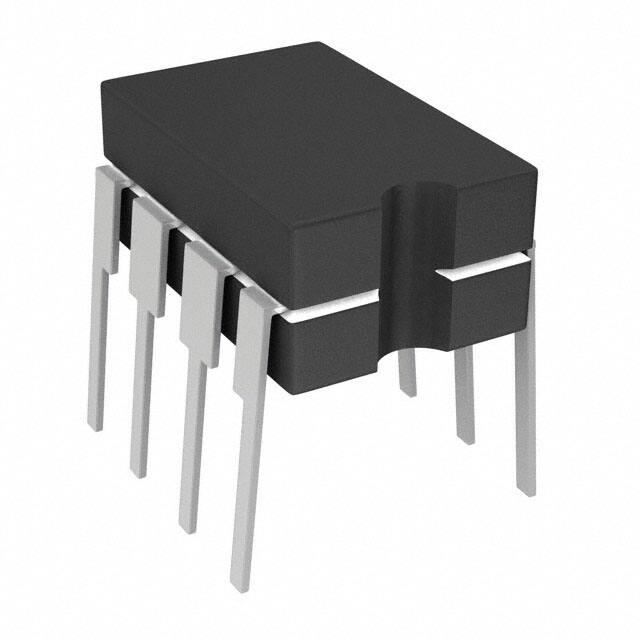
Package Types
8-Pin CERDIP
VDD
INPUT
NC
GND
Note:
1
2
3
4
TC4421M
TC4422M
Applications
They are essentially immune to any form of upset,
except direct overvoltage or over-dissipation. They
cannot be latched, under any conditions, within their
power and voltage ratings. These parts are not subject
to damage or improper operation when up to 5V of
ground bounce is present on their ground terminals.
They can accept, without damage or logic upset, more
than 1A inductive current of either polarity being forced
back into their outputs. In addition, all terminals are fully
protected against up to 4 kV of electrostatic discharge.
TC4421M TC4422M
8
7
6
5
VDD
VDD
OUTPUT
OUTPUT
GND
OUTPUT
OUTPUT
GND
Duplicate pins must both be connected for
proper operation.
DS21934B-page 1
�TC4421M/TC4422M
Functional Block Diagram
VDD
TC4421M
Inverting
300 mV
Output
TC4422M
Non-Inverting
Input
4.7V
GND
Effective
Input
C = 25 pF
DS21934B-page 2
2005-2013 Microchip Technology Inc.
�TC4421M/TC4422M
1.0
ELECTRICAL
CHARACTERISTICS
† Stresses above those listed under “Absolute Maximum
Ratings” may cause permanent damage to the device. These
are stress ratings only and functional operation of the device
at these or any other conditions above those indicated in the
operation sections of the specifications is not implied.
Exposure to Absolute Maximum Rating conditions for
extended periods may affect device reliability.
Absolute Maximum Ratings†
Supply Voltage ..................................................... +20V
Input Voltage .................... (VDD + 0.3V) to (GND – 5V)
Input Current (VIN > VDD)................................... 50 mA
DC CHARACTERISTICS
Electrical Specifications: Unless otherwise noted, TA = +25°C with 4.5V VDD 18V.
Parameters
Sym
Min
Typ
Max
Units
Conditions
Input
Logic ‘1’, High Input Voltage
VIH
2.4
1.8
—
V
Logic ‘0’, Low Input Voltage
VIL
—
1.3
0.8
V
Input Current
IIN
-10
—
+10
µA
0VVINVDD
High Output Voltage
VOH
VDD – 0.025
—
—
V
DC TEST
Low Output Voltage
VOL
—
—
0.025
V
DC TEST
Output Resistance, High
ROH
—
1.4
—
IOUT = 10 mA, VDD = 18V
Output Resistance, Low
ROL
—
0.9
1.7
IOUT = 10 mA, VDD = 18V
Peak Output Current
IPK
—
9.0
—
A
VDD = 18V
Latch-Up Protection
Withstand Reverse Current
IREV
—
>1.5
—
A
Duty cycle2%, t 300 µsec
Rise Time
tR
—
60
75
ns
Figure 4-1, CL = 10,000 pF
Fall Time
tF
—
60
75
ns
Figure 4-1, CL = 10,000 pF
Delay Time
tD1
—
30
60
ns
Figure 4-1
Delay Time
tD2
—
33
60
ns
Figure 4-1
IS
—
—
0.2
55
1.5
150
mA
µA
VIN = 3V
VIN = 0V
VDD
4.5
—
18
V
Output
Switching Time (Note 1)
Power Supply
Power Supply Current
Operating Input Voltage
Note 1:
Switching times ensured by design.
2005-2013 Microchip Technology Inc.
DS21934B-page 3
�TC4421M/TC4422M
DC CHARACTERISTICS (OVER OPERATING TEMPERATURE RANGE)
Electrical Specifications: Unless otherwise noted, over operating temperature range with 4.5V VDD 18V.
Parameters
Sym
Min
Typ
Max
Units
Logic ‘1’, High Input Voltage
VIH
2.4
Logic ‘0’, Low Input Voltage
VIL
—
Input Current
IIN
Conditions
—
—
V
—
0.8
V
-10
—
+10
µA
0VVINVDD
VOH
VDD – 0.025
—
—
V
DC TEST
Low Output Voltage
VOL
—
—
0.025
V
DC TEST
Output Resistance, High
ROH
—
2.4
3.6
IOUT = 10 mA, VDD = 18V
ROL
—
1.8
2.7
IOUT = 10 mA, VDD = 18V
Rise Time
tR
—
60
120
ns
Figure 4-1, CL = 10,000 pF
Fall Time
tF
—
60
120
ns
Figure 4-1, CL = 10,000 pF
Delay Time
tD1
—
50
80
ns
Figure 4-1
Delay Time
tD2
—
65
80
ns
Figure 4-1
IS
—
—
—
—
3
0.2
mA
VIN = 3V
VIN = 0V
VDD
4.5
—
18
V
Input
Output
High Output Voltage
Output Resistance, Low
Switching Time (Note 1)
Power Supply
Power Supply Current
Operating Input Voltage
Note 1:
Switching times ensured by design.
TEMPERATURE CHARACTERISTICS
Electrical Specifications: Unless otherwise noted, all parameters apply with 4.5V VDD 18V.
Parameters
Sym
Min
Typ
Max
Units
TA
-55
—
+125
°C
Conditions
Temperature Ranges
Specified Temperature Range (M)
Maximum Junction Temperature
TJ
—
—
+150
°C
Storage Temperature Range
TA
-65
—
+150
°C
JA
—
150
—
°C/W
Package Thermal Resistances
Thermal Resistance, 8L-CERDIP
DS21934B-page 4
2005-2013 Microchip Technology Inc.
�TC4421M/TC4422M
2.0
TYPICAL PERFORMANCE CURVES
Note:
The graphs and tables provided following this note are a statistical summary based on a limited number of
samples and are provided for informational purposes only. The performance characteristics listed herein
are not tested or guaranteed. In some graphs or tables, the data presented may be outside the specified
operating range (e.g., outside specified power supply range) and therefore outside the warranted range.
Note: Unless otherwise indicated, TA = +25°C with 4.5V VDD 18V.
220
180
200
160
180
22,000 pF
140
22,000 pF
140
120
10,000 pF
100
80
4700 pF
60
120
100
80
10,000 pF
60
4700 pF
40
40
1000 pF
20
0
tFALL (nsec)
tRISE (nsec)
160
20
1000 pF
4
6
FIGURE 2-1:
Voltage.
8
14
10
12
VDD (V)
16
0
18
Rise Time vs. Supply
4
6
8
FIGURE 2-4:
Voltage.
10
12
VDD (V)
14
Fall Time vs. Supply
5V
5V
250
250
10V
200
150
15V
100
tFALL (nsec)
10V
tRISE (nsec)
18
300
300
200
150
15V
100
50
50
0
100
1000
FIGURE 2-2:
Load.
10,000
CLOAD (pF)
0
100
100,000
Rise Time vs. Capacitive
1000
FIGURE 2-5:
Load.
10,000
CLOAD (pF)
100,000
Fall Time vs. Capacitive
50
90
CLOAD = 10,000 pF
VDD = 15V
80
CLOAD = 1000 pF
45
70
TIME (nsec)
TIME (nsec)
16
60
tRISE
50
40
tD2
35
tD1
tFALL
40
30
30
-40
0
40
80
120
25
4
6
TA (°C)
FIGURE 2-3:
Temperature.
Rise and Fall Times vs.
2005-2013 Microchip Technology Inc.
8
10
12
14
16
18
VDD (V)
FIGURE 2-6:
Supply Voltage.
Propagation Delay vs.
DS21934B-page 5
�TC4421M/TC4422M
Note: Unless otherwise indicated, TA = +25°C with 4.5V VDD 18V.
220
180
VDD = 18V
200
160
2 MHz
180
VDD = 18V 47,000 pF
140
10,000 pF
120
63.2 kHz
1.125 MHz
100
80
ISUPPLY (mA)
ISUPPLY (mA)
160
140
632 kHz
60
40
1000
10,000
CLOAD (pF)
120
2 MHz
63.2 kHz
80
1.125 MHz
40
632 kHz
20
200 kHz
ISUPPLY (mA)
ISUPPLY (mA)
140
22,000 pF
10,000 pF
47,000 pF
100
80
60
4700 pF
0.1 μF
20 kHz
20
470 pF
0
100
1000
10,000
CLOAD (pF)
10
100,000
FIGURE 2-8:
Supply Current vs.
Capacitive Load (VDD = 12V).
100
FREQUENCY (kHz)
1000
FIGURE 2-11:
Supply Current vs.
Frequency (VDD = 12V).
100
120
200 kHz
VDD = 6V
VDD = 6V
47,000 pF
100
80
22,000 pF
60
50
63.2 kHz
40
2 MHz
ISUPPLY (mA)
70
30
1000
40
0
90
470 pF
100
FREQUENCY (kHz)
VDD = 12V
160
120
60
4700 pF
180
VDD = 12V
140
100
0.1 μF
60
FIGURE 2-10:
Supply Current vs.
Frequency (VDD = 18V).
180
ISUPPLY (mA)
80
0
10
100,000
FIGURE 2-7:
Supply Current vs.
Capacitive Load (VDD = 18V).
160
100
20
20
0
100
120
40
20 kHz
200 kHz
22,000 pF
80
10,000 pF
4700 pF
60
40
632 kHz
0.1 μF
20
20 kHz
10
20
470 pF
0
100
1000
10,000
CLOAD (pF)
100,000
FIGURE 2-9:
Supply Current vs.
Capactive Load (VDD = 6V).
DS21934B-page 6
0
10
100
FREQUENCY (kHz)
1000
FIGURE 2-12:
Supply Current vs.
Frequency (VDD = 6V).
2005-2013 Microchip Technology Inc.
�TC4421M/TC4422M
Note: Unless otherwise indicated, TA = +25°C with 4.5V VDD 18V.
50
120
VDD = 10V
CLOAD = 10,000 pF
110
100
VDD = 18V
CLOAD = 10,000 pF
VIN = 5V
45
80
TIME (nsec)
TIME (nsec)
90
70
60
tD2
50
40
35
tD2
tD1
30
40
tD1
30
25
20
10
20
-60 -40
0
1
2
3
4
5
6
7
8
INPUT AMPLITUDE (V)
FIGURE 2-13:
Amplitude.
9
10
Propagation Delay vs. Input
-20
0
FIGURE 2-16:
Temperature.
20 40
TA (°C)
60
80
100 120
Propagation Delay vs.
103
10-6
IQUIESCENT (μA)
A•sec
VDD = 18V
10-7
INPUT = 1
102
INPUT = 0
10-8
4
6
8
10
12
VDD (V)
14
16
18
FIGURE 2-17:
vs. Temperature.
20
40
60
80 100 120
Quiescent Supply Current
Crossover Energy vs.
6
6
5.5
5.5
5
5
4.5
4.5
TJ = 150°C
4
RDS(ON) (Ω)
RDS(ON) (Ω)
0
TJ (°C)
NOTE: The values on this graph represent the loss seen
by the driver during a complete cycle. For the loss
in a single transition, divide the stated value by 2.
FIGURE 2-14:
Supply Voltage.
-60 -40 -20
3.5
3
2.5
2
TJ = 150°C
3
2.5
2
TJ = 25°C
1.5
4
3.5
1.5
1
1
0.5
0.5
4
6
8
10
12
VDD (V)
14
16
FIGURE 2-15:
High-State Output
Resistance vs. Supply Voltage.
2005-2013 Microchip Technology Inc.
18
TJ = 25°C
4
6
8
10
12
VDD (V)
14
16
18
FIGURE 2-18:
Low-State Output
Resistance vs. Supply Voltage.
DS21934B-page 7
�TC4421M/TC4422M
3.0
PIN DESCRIPTIONS
The descriptions of the pins are listed in Table 3-1.
TABLE 3-1:
Pin No.
8-Pin CERDIP
3.1
PIN FUNCTION TABLE
Symbol
1
VDD
2
INPUT
Description
Supply input, 4.5V to 18V
Control input, TTL/CMOS-compatible input
3
NC
4
GND
No connection
Ground
5
GND
Ground
6
OUTPUT
7
OUTPUT
8
VDD
CMOS push-pull output
CMOS push-pull output
Supply input, 4.5V to 18V
Supply Input (VDD)
The VDD input is the bias supply for the MOSFET driver
and is rated for 4.5V to 18V with respect to the ground
pin. The VDD input should be bypassed to ground with
a local ceramic capacitor. The value of the capacitor
should be chosen based on the capacitive load that is
being driven. A minimum value of 1.0 µF is suggested.
3.3
The MOSFET driver output is a low-impedance,
CMOS, push-pull style output capable of driving a
capacitive load with 9.0A peak currents. The MOSFET
driver output is capable of withstanding 1.5A peak
reverse currents of either polarity.
3.4
3.2
Control Input
The MOSFET driver input is a high-impedance,
TTL/CMOS-compatible input. The input also has
300 mV of hysteresis between the high and low
thresholds that prevents output glitching even when the
rise and fall time of the input signal is very slow.
DS21934B-page 8
CMOS Push-Pull Output
Ground
The ground pins are the return path for the bias current
and for the high peak currents that discharge the load
capacitor. The ground pins should be tied into a ground
plane or have very short traces to the bias supply
source return.
2005-2013 Microchip Technology Inc.
�TC4421M/TC4422M
4.0
APPLICATIONS INFORMATION
+5V
90%
Input
VDD = 18V
0V
4.7 µF
1
0.1 µF
2
tD1
tD2
tF
tR
90%
90%
Output
8
0.1 µF
Input
+18V
10%
6
10%
10%
0V
Inverting Driver
TC4421M
Output
7
CL = 10,000 pF
+5V
90%
Input
4
5
0V
+18V
Input: 100 kHz,
square wave,
tRISE = tFALL 10 nsec
10%
tD1 90%
tR
Output
0V
10%
tD2
90%
tF
10%
Non-Inverting Driver
TC4422M
FIGURE 4-1:
Switching Time Test Circuits.
2005-2013 Microchip Technology Inc.
DS21934B-page 9
�TC4421M/TC4422M
5.0
PACKAGING INFORMATION
5.1
Package Marking Information
8-Lead CERDIP (300 mil)
XXXXXXXX
XXXXXNNN
YYWW
Legend: XX...X
Y
YY
WW
NNN
e3
*
Note:
DS21934B-page 10
Example:
TC4421
e3
MJA^^256
0542
Customer-specific information
Year code (last digit of calendar year)
Year code (last 2 digits of calendar year)
Week code (week of January 1 is week ‘01’)
Alphanumeric traceability code
Pb-free JEDEC designator for Matte Tin (Sn)
This package is Pb-free. The Pb-free JEDEC designator ( e3 )
can be found on the outer packaging for this package.
In the event the full Microchip part number cannot be marked on one line, it will
be carried over to the next line, thus limiting the number of available
characters for customer-specific information.
2005-2013 Microchip Technology Inc.
�TC4421M/TC4422M
8-Lead Ceramic Dual In-line – 300 mil (CERDIP)
Note:
For the most current package drawings, please see the Microchip Packaging Specification located
at http://www.microchip.com/packaging
E1
2
1
n
D
E
A2
A
c
L
B1
eB
B
A1
Units
Dimension Limits
n
p
Number of Pins
Pitch
Top to Seating Plane
Standoff §
Shoulder to Shoulder Width
Ceramic Pkg. Width
Overall Length
Tip to Seating Plane
Lead Thickness
Upper Lead Width
Lower Lead Width
Overall Row Spacing
*Controlling Parameter
JEDEC Equivalent: MS-030
A
A1
E
E1
D
L
c
B1
B
eB
p
MIN
.160
.020
.290
.230
.370
.125
.008
.045
.016
.320
INCHES*
NOM
8
.100
.180
.030
.305
.265
.385
.163
.012
.055
.018
.360
MAX
.200
.040
.320
.300
.400
.200
.015
.065
.020
.400
MILLIMETERS
NOM
8
2.54
4.06
4.57
0.51
0.77
7.37
7.75
5.84
6.73
9.40
9.78
3.18
4.13
0.20
0.29
1.14
1.40
0.41
0.46
8.13
9.15
MIN
MAX
5.08
1.02
8.13
7.62
10.16
5.08
0.38
1.65
0.51
10.16
Drawing No. C04-010
2005-2013 Microchip Technology Inc.
DS21934B-page 11
�TC4421M/TC4422M
NOTES:
DS21934B-page 12
2005-2013 Microchip Technology Inc.
�TC4421M/TC4422M
APPENDIX A:
REVISION HISTORY
Revision A (February 2005)
• Original Release of this Document.
Revision B (January 2013)
Added a note to each package outline drawing.
2005-2013 Microchip Technology Inc.
DS21934B-page 13
�TC4421M/TC4422M
NOTES:
DS21934B-page 14
2005-2013 Microchip Technology Inc.
�TC4421M/TC4422M
PRODUCT IDENTIFICATION SYSTEM
To order or obtain information, e.g., on pricing or delivery, refer to the factory or the listed sales office.
PART NO.
XX
Device and Temperature
Range
Package
Examples:
a)
TC4421M: 9A High-Speed MOSFET Driver, Inverting,
-55°C to +125°C
TC4422M: 9A High-Speed MOSFET Driver, Non-Inverting,
-55°C to +125°C
Package:
JA = Ceramic Dual In-Line (300 mil Body), 8-lead
2005-2013 Microchip Technology Inc.
9A High-Speed MOSFET
Driver, Inverting,
8LD CERDIP package.
a)
Device and
Temperature Range:
TC4421MJA:
TC4422MJA:
9A High-Speed MOSFET
Driver, Non-Inverting,
8LD CERDIP package.
DS21934B-page 15
�TC4421M/TC4422M
NOTES:
DS21934B-page 16
2005-2013 Microchip Technology Inc.
�Note the following details of the code protection feature on Microchip devices:
•
Microchip products meet the specification contained in their particular Microchip Data Sheet.
•
Microchip believes that its family of products is one of the most secure families of its kind on the market today, when used in the
intended manner and under normal conditions.
•
There are dishonest and possibly illegal methods used to breach the code protection feature. All of these methods, to our
knowledge, require using the Microchip products in a manner outside the operating specifications contained in Microchip’s Data
Sheets. Most likely, the person doing so is engaged in theft of intellectual property.
•
Microchip is willing to work with the customer who is concerned about the integrity of their code.
•
Neither Microchip nor any other semiconductor manufacturer can guarantee the security of their code. Code protection does not
mean that we are guaranteeing the product as “unbreakable.”
Code protection is constantly evolving. We at Microchip are committed to continuously improving the code protection features of our
products. Attempts to break Microchip’s code protection feature may be a violation of the Digital Millennium Copyright Act. If such acts
allow unauthorized access to your software or other copyrighted work, you may have a right to sue for relief under that Act.
Information contained in this publication regarding device
applications and the like is provided only for your convenience
and may be superseded by updates. It is your responsibility to
ensure that your application meets with your specifications.
MICROCHIP MAKES NO REPRESENTATIONS OR
WARRANTIES OF ANY KIND WHETHER EXPRESS OR
IMPLIED, WRITTEN OR ORAL, STATUTORY OR
OTHERWISE, RELATED TO THE INFORMATION,
INCLUDING BUT NOT LIMITED TO ITS CONDITION,
QUALITY, PERFORMANCE, MERCHANTABILITY OR
FITNESS FOR PURPOSE. Microchip disclaims all liability
arising from this information and its use. Use of Microchip
devices in life support and/or safety applications is entirely at
the buyer’s risk, and the buyer agrees to defend, indemnify and
hold harmless Microchip from any and all damages, claims,
suits, or expenses resulting from such use. No licenses are
conveyed, implicitly or otherwise, under any Microchip
intellectual property rights.
Trademarks
The Microchip name and logo, the Microchip logo, dsPIC,
FlashFlex, KEELOQ, KEELOQ logo, MPLAB, PIC, PICmicro,
PICSTART, PIC32 logo, rfPIC, SST, SST Logo, SuperFlash
and UNI/O are registered trademarks of Microchip Technology
Incorporated in the U.S.A. and other countries.
FilterLab, Hampshire, HI-TECH C, Linear Active Thermistor,
MTP, SEEVAL and The Embedded Control Solutions
Company are registered trademarks of Microchip Technology
Incorporated in the U.S.A.
Silicon Storage Technology is a registered trademark of
Microchip Technology Inc. in other countries.
Analog-for-the-Digital Age, Application Maestro, BodyCom,
chipKIT, chipKIT logo, CodeGuard, dsPICDEM,
dsPICDEM.net, dsPICworks, dsSPEAK, ECAN,
ECONOMONITOR, FanSense, HI-TIDE, In-Circuit Serial
Programming, ICSP, Mindi, MiWi, MPASM, MPF, MPLAB
Certified logo, MPLIB, MPLINK, mTouch, Omniscient Code
Generation, PICC, PICC-18, PICDEM, PICDEM.net, PICkit,
PICtail, REAL ICE, rfLAB, Select Mode, SQI, Serial Quad I/O,
Total Endurance, TSHARC, UniWinDriver, WiperLock, ZENA
and Z-Scale are trademarks of Microchip Technology
Incorporated in the U.S.A. and other countries.
SQTP is a service mark of Microchip Technology Incorporated
in the U.S.A.
GestIC and ULPP are registered trademarks of Microchip
Technology Germany II GmbH & Co. & KG, a subsidiary of
Microchip Technology Inc., in other countries.
All other trademarks mentioned herein are property of their
respective companies.
© 2005-2013, Microchip Technology Incorporated, Printed in
the U.S.A., All Rights Reserved.
Printed on recycled paper.
ISBN: 9781620769171
QUALITY MANAGEMENT SYSTEM
CERTIFIED BY DNV
== ISO/TS 16949 ==
2005-2013 Microchip Technology Inc.
Microchip received ISO/TS-16949:2009 certification for its worldwide
headquarters, design and wafer fabrication facilities in Chandler and
Tempe, Arizona; Gresham, Oregon and design centers in California
and India. The Company’s quality system processes and procedures
are for its PIC® MCUs and dsPIC® DSCs, KEELOQ® code hopping
devices, Serial EEPROMs, microperipherals, nonvolatile memory and
analog products. In addition, Microchip’s quality system for the design
and manufacture of development systems is ISO 9001:2000 certified.
DS21934B-page 17
�Worldwide Sales and Service
AMERICAS
ASIA/PACIFIC
ASIA/PACIFIC
EUROPE
Corporate Office
2355 West Chandler Blvd.
Chandler, AZ 85224-6199
Tel: 480-792-7200
Fax: 480-792-7277
Technical Support:
http://www.microchip.com/
support
Web Address:
www.microchip.com
Asia Pacific Office
Suites 3707-14, 37th Floor
Tower 6, The Gateway
Harbour City, Kowloon
Hong Kong
Tel: 852-2401-1200
Fax: 852-2401-3431
India - Bangalore
Tel: 91-80-3090-4444
Fax: 91-80-3090-4123
India - New Delhi
Tel: 91-11-4160-8631
Fax: 91-11-4160-8632
Austria - Wels
Tel: 43-7242-2244-39
Fax: 43-7242-2244-393
Denmark - Copenhagen
Tel: 45-4450-2828
Fax: 45-4485-2829
India - Pune
Tel: 91-20-2566-1512
Fax: 91-20-2566-1513
France - Paris
Tel: 33-1-69-53-63-20
Fax: 33-1-69-30-90-79
Japan - Osaka
Tel: 81-6-6152-7160
Fax: 81-6-6152-9310
Germany - Munich
Tel: 49-89-627-144-0
Fax: 49-89-627-144-44
Atlanta
Duluth, GA
Tel: 678-957-9614
Fax: 678-957-1455
Boston
Westborough, MA
Tel: 774-760-0087
Fax: 774-760-0088
Chicago
Itasca, IL
Tel: 630-285-0071
Fax: 630-285-0075
Cleveland
Independence, OH
Tel: 216-447-0464
Fax: 216-447-0643
Dallas
Addison, TX
Tel: 972-818-7423
Fax: 972-818-2924
Detroit
Farmington Hills, MI
Tel: 248-538-2250
Fax: 248-538-2260
Indianapolis
Noblesville, IN
Tel: 317-773-8323
Fax: 317-773-5453
Los Angeles
Mission Viejo, CA
Tel: 949-462-9523
Fax: 949-462-9608
Santa Clara
Santa Clara, CA
Tel: 408-961-6444
Fax: 408-961-6445
Toronto
Mississauga, Ontario,
Canada
Tel: 905-673-0699
Fax: 905-673-6509
Australia - Sydney
Tel: 61-2-9868-6733
Fax: 61-2-9868-6755
China - Beijing
Tel: 86-10-8569-7000
Fax: 86-10-8528-2104
China - Chengdu
Tel: 86-28-8665-5511
Fax: 86-28-8665-7889
China - Chongqing
Tel: 86-23-8980-9588
Fax: 86-23-8980-9500
Netherlands - Drunen
Tel: 31-416-690399
Fax: 31-416-690340
Korea - Daegu
Tel: 82-53-744-4301
Fax: 82-53-744-4302
Spain - Madrid
Tel: 34-91-708-08-90
Fax: 34-91-708-08-91
China - Hangzhou
Tel: 86-571-2819-3187
Fax: 86-571-2819-3189
Korea - Seoul
Tel: 82-2-554-7200
Fax: 82-2-558-5932 or
82-2-558-5934
China - Hong Kong SAR
Tel: 852-2943-5100
Fax: 852-2401-3431
Malaysia - Kuala Lumpur
Tel: 60-3-6201-9857
Fax: 60-3-6201-9859
China - Nanjing
Tel: 86-25-8473-2460
Fax: 86-25-8473-2470
Malaysia - Penang
Tel: 60-4-227-8870
Fax: 60-4-227-4068
China - Qingdao
Tel: 86-532-8502-7355
Fax: 86-532-8502-7205
Philippines - Manila
Tel: 63-2-634-9065
Fax: 63-2-634-9069
China - Shanghai
Tel: 86-21-5407-5533
Fax: 86-21-5407-5066
Singapore
Tel: 65-6334-8870
Fax: 65-6334-8850
China - Shenyang
Tel: 86-24-2334-2829
Fax: 86-24-2334-2393
Taiwan - Hsin Chu
Tel: 886-3-5778-366
Fax: 886-3-5770-955
China - Shenzhen
Tel: 86-755-8864-2200
Fax: 86-755-8203-1760
Taiwan - Kaohsiung
Tel: 886-7-213-7828
Fax: 886-7-330-9305
China - Wuhan
Tel: 86-27-5980-5300
Fax: 86-27-5980-5118
Taiwan - Taipei
Tel: 886-2-2508-8600
Fax: 886-2-2508-0102
China - Xian
Tel: 86-29-8833-7252
Fax: 86-29-8833-7256
Thailand - Bangkok
Tel: 66-2-694-1351
Fax: 66-2-694-1350
UK - Wokingham
Tel: 44-118-921-5869
Fax: 44-118-921-5820
China - Xiamen
Tel: 86-592-2388138
Fax: 86-592-2388130
China - Zhuhai
Tel: 86-756-3210040
Fax: 86-756-3210049
DS21934B-page 18
Italy - Milan
Tel: 39-0331-742611
Fax: 39-0331-466781
Japan - Tokyo
Tel: 81-3-6880- 3770
Fax: 81-3-6880-3771
11/29/12
2005-2013 Microchip Technology Inc.
�


 工商网监
湘ICP备2023018690号
工商网监
湘ICP备2023018690号
